WO2012173122A1 - プラズマエッチング方法 - Google Patents
プラズマエッチング方法 Download PDFInfo
- Publication number
- WO2012173122A1 WO2012173122A1 PCT/JP2012/065034 JP2012065034W WO2012173122A1 WO 2012173122 A1 WO2012173122 A1 WO 2012173122A1 JP 2012065034 W JP2012065034 W JP 2012065034W WO 2012173122 A1 WO2012173122 A1 WO 2012173122A1
- Authority
- WO
- WIPO (PCT)
- Prior art keywords
- etching
- gas
- flow rate
- silicon layer
- plasma
- Prior art date
- Legal status (The legal status is an assumption and is not a legal conclusion. Google has not performed a legal analysis and makes no representation as to the accuracy of the status listed.)
- Ceased
Links
Images







Classifications
-
- H—ELECTRICITY
- H10—SEMICONDUCTOR DEVICES; ELECTRIC SOLID-STATE DEVICES NOT OTHERWISE PROVIDED FOR
- H10P—GENERIC PROCESSES OR APPARATUS FOR THE MANUFACTURE OR TREATMENT OF DEVICES COVERED BY CLASS H10
- H10P50/00—Etching of wafers, substrates or parts of devices
- H10P50/20—Dry etching; Plasma etching; Reactive-ion etching
- H10P50/24—Dry etching; Plasma etching; Reactive-ion etching of semiconductor materials
- H10P50/242—Dry etching; Plasma etching; Reactive-ion etching of semiconductor materials of Group IV materials
-
- H—ELECTRICITY
- H01—ELECTRIC ELEMENTS
- H01J—ELECTRIC DISCHARGE TUBES OR DISCHARGE LAMPS
- H01J37/00—Discharge tubes with provision for introducing objects or material to be exposed to the discharge, e.g. for the purpose of examination or processing thereof
- H01J37/32—Gas-filled discharge tubes
- H01J37/32009—Arrangements for generation of plasma specially adapted for examination or treatment of objects, e.g. plasma sources
- H01J37/32082—Radio frequency generated discharge
- H01J37/32137—Radio frequency generated discharge controlling of the discharge by modulation of energy
- H01J37/32155—Frequency modulation
- H01J37/32165—Plural frequencies
-
- H—ELECTRICITY
- H01—ELECTRIC ELEMENTS
- H01J—ELECTRIC DISCHARGE TUBES OR DISCHARGE LAMPS
- H01J37/00—Discharge tubes with provision for introducing objects or material to be exposed to the discharge, e.g. for the purpose of examination or processing thereof
- H01J37/32—Gas-filled discharge tubes
- H01J37/32431—Constructional details of the reactor
- H01J37/3244—Gas supply means
- H01J37/32449—Gas control, e.g. control of the gas flow
-
- H—ELECTRICITY
- H01—ELECTRIC ELEMENTS
- H01J—ELECTRIC DISCHARGE TUBES OR DISCHARGE LAMPS
- H01J37/00—Discharge tubes with provision for introducing objects or material to be exposed to the discharge, e.g. for the purpose of examination or processing thereof
- H01J37/32—Gas-filled discharge tubes
- H01J37/32431—Constructional details of the reactor
- H01J37/3266—Magnetic control means
-
- H—ELECTRICITY
- H01—ELECTRIC ELEMENTS
- H01J—ELECTRIC DISCHARGE TUBES OR DISCHARGE LAMPS
- H01J37/00—Discharge tubes with provision for introducing objects or material to be exposed to the discharge, e.g. for the purpose of examination or processing thereof
- H01J37/32—Gas-filled discharge tubes
- H01J37/32431—Constructional details of the reactor
- H01J37/3266—Magnetic control means
- H01J37/32669—Particular magnets or magnet arrangements for controlling the discharge
-
- H—ELECTRICITY
- H10—SEMICONDUCTOR DEVICES; ELECTRIC SOLID-STATE DEVICES NOT OTHERWISE PROVIDED FOR
- H10P—GENERIC PROCESSES OR APPARATUS FOR THE MANUFACTURE OR TREATMENT OF DEVICES COVERED BY CLASS H10
- H10P50/00—Etching of wafers, substrates or parts of devices
- H10P50/20—Dry etching; Plasma etching; Reactive-ion etching
- H10P50/24—Dry etching; Plasma etching; Reactive-ion etching of semiconductor materials
- H10P50/242—Dry etching; Plasma etching; Reactive-ion etching of semiconductor materials of Group IV materials
- H10P50/244—Dry etching; Plasma etching; Reactive-ion etching of semiconductor materials of Group IV materials comprising alternated and repeated etching and passivation steps
-
- H—ELECTRICITY
- H10—SEMICONDUCTOR DEVICES; ELECTRIC SOLID-STATE DEVICES NOT OTHERWISE PROVIDED FOR
- H10P—GENERIC PROCESSES OR APPARATUS FOR THE MANUFACTURE OR TREATMENT OF DEVICES COVERED BY CLASS H10
- H10P50/00—Etching of wafers, substrates or parts of devices
- H10P50/20—Dry etching; Plasma etching; Reactive-ion etching
- H10P50/26—Dry etching; Plasma etching; Reactive-ion etching of conductive or resistive materials
- H10P50/262—Dry etching; Plasma etching; Reactive-ion etching of conductive or resistive materials by physical means only
- H10P50/263—Dry etching; Plasma etching; Reactive-ion etching of conductive or resistive materials by physical means only of silicon-containing layers
-
- H—ELECTRICITY
- H10—SEMICONDUCTOR DEVICES; ELECTRIC SOLID-STATE DEVICES NOT OTHERWISE PROVIDED FOR
- H10P—GENERIC PROCESSES OR APPARATUS FOR THE MANUFACTURE OR TREATMENT OF DEVICES COVERED BY CLASS H10
- H10P50/00—Etching of wafers, substrates or parts of devices
- H10P50/20—Dry etching; Plasma etching; Reactive-ion etching
- H10P50/26—Dry etching; Plasma etching; Reactive-ion etching of conductive or resistive materials
- H10P50/264—Dry etching; Plasma etching; Reactive-ion etching of conductive or resistive materials by chemical means
- H10P50/266—Dry etching; Plasma etching; Reactive-ion etching of conductive or resistive materials by chemical means by vapour etching only
- H10P50/267—Dry etching; Plasma etching; Reactive-ion etching of conductive or resistive materials by chemical means by vapour etching only using plasmas
- H10P50/268—Dry etching; Plasma etching; Reactive-ion etching of conductive or resistive materials by chemical means by vapour etching only using plasmas of silicon-containing layers
-
- H—ELECTRICITY
- H10—SEMICONDUCTOR DEVICES; ELECTRIC SOLID-STATE DEVICES NOT OTHERWISE PROVIDED FOR
- H10P—GENERIC PROCESSES OR APPARATUS FOR THE MANUFACTURE OR TREATMENT OF DEVICES COVERED BY CLASS H10
- H10P50/00—Etching of wafers, substrates or parts of devices
- H10P50/69—Etching of wafers, substrates or parts of devices using masks for semiconductor materials
- H10P50/691—Etching of wafers, substrates or parts of devices using masks for semiconductor materials for Group V materials or Group III-V materials
-
- H—ELECTRICITY
- H10—SEMICONDUCTOR DEVICES; ELECTRIC SOLID-STATE DEVICES NOT OTHERWISE PROVIDED FOR
- H10P—GENERIC PROCESSES OR APPARATUS FOR THE MANUFACTURE OR TREATMENT OF DEVICES COVERED BY CLASS H10
- H10P50/00—Etching of wafers, substrates or parts of devices
- H10P50/69—Etching of wafers, substrates or parts of devices using masks for semiconductor materials
- H10P50/691—Etching of wafers, substrates or parts of devices using masks for semiconductor materials for Group V materials or Group III-V materials
- H10P50/692—Etching of wafers, substrates or parts of devices using masks for semiconductor materials for Group V materials or Group III-V materials characterised by their composition, e.g. multilayer masks or materials
-
- H—ELECTRICITY
- H10—SEMICONDUCTOR DEVICES; ELECTRIC SOLID-STATE DEVICES NOT OTHERWISE PROVIDED FOR
- H10P—GENERIC PROCESSES OR APPARATUS FOR THE MANUFACTURE OR TREATMENT OF DEVICES COVERED BY CLASS H10
- H10P72/00—Handling or holding of wafers, substrates or devices during manufacture or treatment thereof
- H10P72/04—Apparatus for manufacture or treatment
- H10P72/0402—Apparatus for fluid treatment
- H10P72/0418—Apparatus for fluid treatment for etching
- H10P72/0421—Apparatus for fluid treatment for etching for drying etching
-
- H—ELECTRICITY
- H10—SEMICONDUCTOR DEVICES; ELECTRIC SOLID-STATE DEVICES NOT OTHERWISE PROVIDED FOR
- H10W—GENERIC PACKAGES, INTERCONNECTIONS, CONNECTORS OR OTHER CONSTRUCTIONAL DETAILS OF DEVICES COVERED BY CLASS H10
- H10W20/00—Interconnections in chips, wafers or substrates
- H10W20/01—Manufacture or treatment
- H10W20/021—Manufacture or treatment of interconnections within wafers or substrates
- H10W20/023—Manufacture or treatment of interconnections within wafers or substrates the interconnections being through-semiconductor vias
-
- H—ELECTRICITY
- H10—SEMICONDUCTOR DEVICES; ELECTRIC SOLID-STATE DEVICES NOT OTHERWISE PROVIDED FOR
- H10W—GENERIC PACKAGES, INTERCONNECTIONS, CONNECTORS OR OTHER CONSTRUCTIONAL DETAILS OF DEVICES COVERED BY CLASS H10
- H10W20/00—Interconnections in chips, wafers or substrates
- H10W20/01—Manufacture or treatment
- H10W20/021—Manufacture or treatment of interconnections within wafers or substrates
- H10W20/023—Manufacture or treatment of interconnections within wafers or substrates the interconnections being through-semiconductor vias
- H10W20/0242—Manufacture or treatment of interconnections within wafers or substrates the interconnections being through-semiconductor vias comprising etching via holes from the back sides of the chips, wafers or substrates
-
- H—ELECTRICITY
- H10—SEMICONDUCTOR DEVICES; ELECTRIC SOLID-STATE DEVICES NOT OTHERWISE PROVIDED FOR
- H10W—GENERIC PACKAGES, INTERCONNECTIONS, CONNECTORS OR OTHER CONSTRUCTIONAL DETAILS OF DEVICES COVERED BY CLASS H10
- H10W20/00—Interconnections in chips, wafers or substrates
- H10W20/01—Manufacture or treatment
- H10W20/021—Manufacture or treatment of interconnections within wafers or substrates
- H10W20/023—Manufacture or treatment of interconnections within wafers or substrates the interconnections being through-semiconductor vias
- H10W20/0245—Manufacture or treatment of interconnections within wafers or substrates the interconnections being through-semiconductor vias comprising use of blind vias during the manufacture
-
- H—ELECTRICITY
- H01—ELECTRIC ELEMENTS
- H01J—ELECTRIC DISCHARGE TUBES OR DISCHARGE LAMPS
- H01J2237/00—Discharge tubes exposing object to beam, e.g. for analysis treatment, etching, imaging
- H01J2237/32—Processing objects by plasma generation
- H01J2237/33—Processing objects by plasma generation characterised by the type of processing
- H01J2237/334—Etching
Definitions
- the present invention relates to a plasma etching method for performing etching using plasma.
- the laminated semiconductor device includes an electrode formed through a substrate made of, for example, a silicon layer, and is electrically connected through this electrode.
- a resist is applied to the substrate using a coating device, exposed using an exposure device, and then developed by a developing device to form a resist pattern.
- the formed resist pattern is used, for example, as a mask when etching the substrate, thereby forming a hole such as a through hole or a via hole. After the hole is formed, the resist remaining on the substrate is removed by ashing.
- etching of a substrate made of a silicon layer is performed by generating plasma from an etching gas containing a fluorine-containing compound gas such as SF 6 gas and the generated plasma.
- a fluorine-containing compound gas such as SF 6 gas
- the hole described above is usually required to be formed to a depth of about 100 ⁇ m.
- the etching gas is composed of only a fluorine-containing compound gas such as SF 6 gas, etching with plasma generated from the etching gas tends to be isotropic etching. Thereby, the side wall of the resist pattern is also easily etched. As a result, a so-called undercut is likely to occur in which the etching region extends in the lateral direction, and it becomes difficult to maintain the shape of the sidewall of the hole portion vertically.
- the protective film can withstand prolonged exposure to plasma.
- the protective film to be formed must be thick. This increases the time required for the step of forming the protective film, so that the overall time required for plasma etching further increases. As a result, the silicon layer cannot be etched at high speed, and the productivity of the semiconductor device decreases.
- the ratio of the thickness of the protective film formed on the side wall of the hole to the diameter of the hole is increased. For this reason, it becomes difficult to obtain a vertical sidewall shape due to variations in the thickness of the protective film along the depth direction of the hole. Further, as the diameter of the hole to be formed becomes smaller, the etching gas for depositing the protective film hardly reaches the side wall of the hole, and the protective film becomes difficult to form. As a result, undercut occurs, and it becomes difficult to keep the shape of the side wall of the hole perpendicular to the surface of the substrate.
- an object of the present invention is to form the side wall of the hole portion perpendicular to the surface of the substrate when the hole portion is formed by etching the surface of the substrate on which the resist pattern is formed. Another object is to provide a plasma etching method for etching a silicon layer at high speed.
- the present invention is characterized by the following measures.
- a processing container in which a substrate to be processed which includes a silicon layer and has a resist layer patterned in a predetermined pattern formed above the silicon layer.
- a plasma etching method in which an etching gas containing an oxygen gas and a sulfur fluoride gas is supplied at a predetermined flow rate, and the silicon layer is etched using the resist layer as a mask by plasma generated from the supplied etching gas.
- a process comprising a silicon layer and a substrate to be processed in which a resist layer patterned in a predetermined pattern is formed above the silicon layer.
- Plasma that etches the silicon layer using the resist layer as a mask with plasma obtained by supplying an etching gas containing oxygen gas and sulfur fluoride gas at a predetermined flow rate into the container, and converting the supplied etching gas into plasma.
- the etching method when etching is started, when the flow rate ratio of oxygen gas to sulfur fluoride gas is set to the first flow rate ratio, plasma obtained by converting the etching gas into plasma is reacted with the resist layer.
- Deposition rate for depositing a protective film on the surface of the substrate to be processed, and etching for etching the protective film A first magnetic field larger than a predetermined magnetic field having the same degree is applied to the substrate to be processed, and the flow rate ratio is set to the first flow rate ratio, and the surface of the substrate to be processed is A protective film is deposited, and the etching rate is reduced by reducing the flow rate of oxygen gas in the state where the first magnetic field is applied to the substrate to be processed as the etching progresses.
- a plasma etching method is provided that is relatively large.
- a process comprising a silicon layer and a substrate to be processed in which a resist layer patterned in a predetermined pattern is formed above the silicon layer.
- An etching gas containing oxygen gas and sulfur fluoride gas is supplied into the container at a predetermined flow rate, and the silicon layer is etched using the resist layer as a mask with plasma obtained by converting the supplied etching gas into plasma.
- oxygen gas generated by converting the etching gas into plasma when the flow rate ratio of oxygen gas to sulfur fluoride gas is set to the first flow rate ratio.
- a protective film is deposited on the surface of the resist layer and the side wall of the hole to be formed. And applying a first magnetic field larger than a predetermined magnetic field such that the deposition rate to be applied and the etching rate for etching the protective film are equal to each other, and the flow rate ratio to the first flow rate ratio.
- the protective film is deposited on the surface of the resist layer and the sidewall of the hole, and the first magnetic field is applied to the substrate to be processed as the depth of the hole increases.
- a plasma etching method is provided, in which the etching rate is made relatively higher than the deposition rate by reducing the flow rate of oxygen gas in a state where is applied.
- the sidewall of the hole is formed perpendicular to the surface of the substrate and the silicon layer is etched at a high speed. be able to.
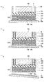
- FIG. 1 It is a schematic sectional drawing which shows the structure of the plasma etching apparatus suitable for the plasma etching method which concerns on 1st Embodiment. It is a cross-sectional view which shows typically the structure of the dipole ring magnet attached to the plasma etching apparatus of FIG. It is a figure for demonstrating the electric field and magnetic field which are formed in the chamber of the plasma etching apparatus of FIG. It is a figure which shows the structure of the etching gas supply part in the etching apparatus of FIG. It is sectional drawing (the 1) which shows typically the state of the wafer in each process of the plasma etching method which concerns on 1st Embodiment.
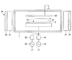
- FIG. 1 is a schematic cross-sectional view showing a configuration of a plasma etching apparatus suitable for the plasma etching method according to the present embodiment.
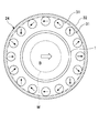
- FIG. 2 is a cross-sectional view schematically showing the configuration of the dipole ring magnet 24.
- FIG. 3 is a diagram for explaining an electric field and a magnetic field formed in the chamber 1.
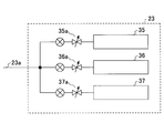
- FIG. 4 is a diagram showing the configuration of the etching gas supply unit 23.
- the plasma etching apparatus is configured as a magnetron reactive ion etching (RIE) type plasma etching apparatus, and has a chamber (processing vessel) 1 made of a metal such as aluminum or stainless steel.
- RIE magnetron reactive ion etching
- a table or susceptor 2 for mounting a silicon wafer (hereinafter simply referred to as “wafer”) W as a substrate to be processed is provided.
- the susceptor 2 is made of, for example, aluminum, and is supported by a support portion 4 made of a conductor via an insulating member 3.
- a focus ring 5 made of, for example, quartz is disposed around the upper surface of the susceptor 2.
- an electrostatic chuck 6 for holding the wafer W by electrostatic attraction is provided.
- the susceptor 2 and the support part 4 can be lifted and lowered by a lifting mechanism including a ball screw 7, and a lifting drive part (not shown) provided below the support part 4 is covered with a bellows 8 made of stainless steel. Yes.
- a bellows cover 9 is provided outside the bellows 8.
- the lower surface of the focus ring 5 is connected to the baffle plate 10, and the focus ring 5 is electrically connected to the chamber 1 through the baffle plate 10, the support portion 4 and the bellows 8.
- the chamber 1 is grounded.
- the susceptor 2 and the support part 4 are equivalent to the support part in this invention.
- the chamber 1 has an upper part 1a having a small diameter and a lower part 1b having a larger diameter than the upper part 1a.
- An exhaust port 11 is formed in the side wall of the lower portion 1b of the chamber 1, and an exhaust system 12 is connected to the exhaust port 11 through an exhaust pipe.
- a gate valve 13 for opening and closing the loading / unloading port for the wafer W is also attached to the side wall of the lower portion 1 b of the chamber 1.
- a first high-frequency power source 15 for plasma generation and reactive ion etching (RIE) is electrically connected to the susceptor 2 through a matching unit 14.
- the first high frequency power supply 15 supplies a first high frequency power having a first frequency of 40 MHz, for example, to the lower electrode, that is, the susceptor 2.
- a shower head 20 described later is provided on the ceiling of the chamber 1 as an upper electrode held at a ground potential. Accordingly, the first high frequency power from the first high frequency power supply 15 is supplied between the susceptor 2 and the shower head 20.
- the susceptor 2 is electrically connected to the first high frequency power supply 15 in parallel with the second high frequency power supply 26 via a separate matching unit 25.
- the second high-frequency power source 26 supplies a second high-frequency power having a second frequency lower than the first frequency of the first high-frequency power supplied from the first high-frequency power source 15, for example, 3.6 MHz, to the susceptor. 2 is supplied in a superimposed manner.
- the second high-frequency power from the second high-frequency power source 26 is for preventing the side wall roughness of the hole from occurring when the hole is formed, as will be described later.
- the electrostatic chuck 6 is obtained by sandwiching an electrode 6a made of a conductive film between a pair of insulating sheets 6b, and a DC power source 16 is electrically connected to the electrode 6a.
- the wafer W can be attracted and held by electrostatic attraction by a DC voltage from the DC power source 16.
- a refrigerant chamber 17 extending in the circumferential direction is provided.
- a refrigerant of a predetermined temperature for example, cooling water
- the processing temperature of the wafer W on the susceptor 2 can be controlled by the temperature of the refrigerant.
- the temperature of the susceptor 2 is preferably as low as possible. For example, a coolant of about ⁇ 30 ° C. may be used.
- a cooling gas such as He gas from the gas introduction mechanism 18 is supplied between the upper surface of the electrostatic chuck 6 and the rear surface of the wafer W via the gas supply line 19.
- the gas introduction mechanism 18 can independently control the gas pressure, that is, the back pressure, at the wafer central portion and the wafer peripheral portion in order to improve the uniformity of the etching process within the wafer surface.
- the shower head 20 at the ceiling is provided with a large number of gas discharge ports 22 on the lower surface facing the upper surface of the susceptor 2 in parallel.
- a buffer chamber 21 is provided inside the gas discharge surface, and a gas supply pipe 23 a from the etching gas supply unit 23 is connected to the gas inlet 20 a of the buffer chamber 21.
- a dipole ring magnet 24 extending annularly or concentrically is disposed around the upper portion 1 a of the chamber 1.
- the dipole ring magnet 24 includes a plurality of, for example, sixteen anisotropic segment columnar magnets 31 arranged at regular intervals in the circumferential direction in a casing 32 made of a ring-shaped magnetic body. Do it.
- the arrow shown in each anisotropic segment columnar magnet 31 indicates the direction of magnetization, and the direction of magnetization of each anisotropic segment columnar magnet 31 is gradually changed along the circumferential direction as shown in the figure. By shifting, a uniform horizontal magnetic field B directed in one direction as a whole can be formed.
- a vertical RF electric field EL is formed by the first high frequency power supply 15, and by the dipole ring magnet 24.
- a horizontal magnetic field B is formed.
- etching gas a mixed gas of a fluorine compound gas made of sulfur fluoride or carbon fluoride and oxygen (O 2 ) gas can be used as the etching gas.
- fluorine compound gas it is preferable to use a gas having a large number of fluorine atoms in one molecule, for example, sulfur hexafluoride (SF 6 ) gas or sulfur defluoride (S 2 F 10 ) gas.
- SF 6 sulfur hexafluoride
- S 2 F 10 sulfur defluoride
- a silicon fluoride gas such as silicon tetrafluoride (SiF 4 ) gas may be added to the etching gas. Therefore, as schematically shown in FIG. 4, the etching gas supply unit 23 includes, for example, an SF 6 gas source 35, an O 2 gas source 36, and an SiF 4 gas source 37. 36a and 37a are provided so as to be individually controllable.
- the operation of the plasma etching apparatus having the above configuration is comprehensively controlled by the control unit 40.
- the control unit 40 includes a process controller 41 that includes a CPU and controls each unit of the plasma etching apparatus, a user interface 42, and a storage unit 43.
- the user interface 42 is composed of a keyboard on which a process manager inputs commands to manage the plasma etching apparatus, a display that visualizes and displays the operating status of the plasma etching apparatus, and the like.
- the storage unit 43 stores a recipe in which a control program (software) for realizing various processes executed by the plasma etching apparatus under the control of the process controller 41 and processing condition data are stored. Then, if necessary, an arbitrary recipe is called from the storage unit 43 by an instruction from the user interface 42 and executed by the process controller 41, so that a desired process in the plasma etching apparatus can be performed under the control of the process controller 41. Processing is performed.
- recipes such as control programs and processing condition data may be stored in computer-readable computer storage media (for example, hard disks, CDs, flexible disks, semiconductor memories, etc.). Is possible.
- recipes such as control programs and processing condition data can be transmitted from other devices as needed via, for example, a dedicated line and used online.
- the gate valve 13 is opened, a wafer W made of a silicon layer as a substrate to be processed is loaded into the chamber 1, and the top of the susceptor 2 is loaded. Placed on. Next, the susceptor 2 on which the wafer W is placed is raised to the height position shown in the figure, and the inside of the chamber 1 is exhausted through the exhaust port 11 by the vacuum pump of the exhaust system 12. Then, the etching gas is introduced into the chamber 1 from the etching gas supply unit 23 at a predetermined flow rate, and the pressure in the chamber 1 is set to a set value.
- high frequency power is applied from the first high frequency power supply 15 to the susceptor 2 with a predetermined power.
- a DC voltage is applied from the DC power source 16 to the electrode 6 a of the electrostatic chuck 6 to support the wafer W by fixing it to the susceptor 2.
- the etching gas discharged from the shower head 20 is converted into plasma by magnetron discharge, and the plasma that has been converted into plasma is irradiated onto the wafer W. Then, the wafer W is etched by radicals and ions contained in the irradiated plasma.
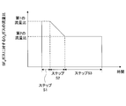
- FIG. 9A is a graph schematically showing a change over time in the flow rate ratio of O 2 gas to SF 6 gas in the step of etching the silicon layer.
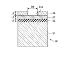
- 5 to 8 show an enlarged region in the vicinity of one opening 54a on the wafer W.
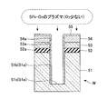
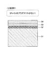
- the wafer W has a first hard mask film 52, a second hard mask film 53, and a mask film 54 on a base 51 made of, for example, a single crystal silicon (Si) layer from below. They are stacked in this order.
- a silicon nitride (SiN) film having a thickness dimension t1 can be used, and the thickness dimension t1 can be set to 0.5 ⁇ m, for example.
- a silicon oxide (SiOx) film having a thickness dimension t2 can be used, and the thickness dimension t2 can be set to 0.5 ⁇ m, for example.
- a resist layer having a thickness dimension t3 can be used, and the thickness dimension t3 can be set to 2.5 ⁇ m, for example.
- a circular opening 54a having an opening diameter (diameter dimension) D1 of, for example, 8 ⁇ m is patterned in a plurality of locations on the mask film 54 by performing a photolithography process in advance.
- the first hard mask film 52 is a silicon oxide (SiOx) film and the second hard mask film 53 is a silicon nitride (SiN) film. It may be.
- Such a wafer W is loaded into the chamber 1 and placed on the susceptor 2 as described above.
- Step S1 corresponds to the first step in the present invention.
- the first flow rate ratio is preferably 0.9 to 1.1. Thus, it is possible to substantially equalize the flow rates and O 2 gas of SF 6 gas.
- the etching gas is introduced into the chamber 1 from the etching gas supply unit 23 at a predetermined flow rate, and the pressure in the chamber 1 is set to a set value.
- etching gas SF 6 gas and O 2 gas are introduced into the chamber 1 at a predetermined flow rate.
- silicon fluoride (SiF 4 ) gas and hydrogen bromide (HBr) gas may be added to the etching gas.
- the first high frequency power supply 15 supplies the first high frequency power to the susceptor 2 in a state where the wafer W is supported by the DC power supply 16 fixed to the susceptor 2 by electrostatic attraction. Then, the etching gas discharged from the shower head 20 is converted into plasma by magnetron discharge, and the plasma W is irradiated onto the wafer W.
- the second hard mask film 53 and the first hard mask film 52 on the lower layer side are respectively formed in the openings 54 a of the mask film 54. Openings 53 a and 52 a are formed, and a hole 51 a is formed in the base 51.
- the selectivity which is the ratio of the etching rates of the second hard mask film 53, the first hard mask film 52, and the silicon layer 51 to the etching rate of the mask film 54, is considerable. large. Therefore, in FIG. 6, illustration of the change in the film thickness of the mask film 54 is omitted (the same applies to FIG. 7).
- fluorine radical F * is generated when the etching gas is turned into plasma.
- fluorine radical F * reaches the hole 51a, the following reaction formula (1) 4F * + Si ⁇ SiF 4 (1)
- SiF 4 is produced by the reaction of the fluorine radical F * with Si. Then, the generated SiF 4 is discharged out of the hole 51a, whereby the silicon layer 51 is etched.
- oxygen radicals O * are generated when the etching gas is turned into plasma.
- SiF 4 generated by the above reaction formula (1) reacts with any plasma, or when fluorine radical F * and Si react, a radical SiFx * of silicon fluoride is generated.
- the following reaction formula (2) O * + SiFx * ⁇ SiOFx (2)
- the SiO radical protective film 55 (for example, SiOFx) is deposited by the reaction of the oxygen radical O * with the radical SiFx * of silicon fluoride.
- the protective film 55 includes an upper surface of the mask film 54, a sidewall of the opening 54 a of the mask film 54, a sidewall of the opening 53 a of the second hard mask film 53, and the first hard mask film 52.
- the bottom surface 51c of the hole 51a of the silicon layer 51 is farthest from the surface of the wafer W, compared with the portion from the upper surface of the mask film 54 to the side wall 51b of the hole 51a of the silicon layer 51, Deposition rate is low.
- anisotropic etching can be performed in which the etching rate for etching the hole 51a in the depth direction is larger than the etching rate for etching the hole 51a in the lateral direction, and the side wall 51b of the hole 51a is formed on the wafer W. It can be perpendicular to the surface.
- step S1 may be divided into step S1-1 and step S1-2 as shown in FIG. 9B.
- Step S1-1 corresponds to the fourth step in the present invention
- step S1-2 corresponds to the fifth step in the present invention.
- step S1-1 the first high frequency power having the first frequency is supplied to the susceptor 2, and the second high frequency power having the second frequency lower than the first frequency is supplied.
- the silicon layer 51 is etched. Thereby, since the natural oxide film or resist residue on the Si surface can be etched efficiently, it is possible to prevent the roughening of the side wall of the hole 51a caused by them.
- step S1-2 the supply of the second high frequency power to the susceptor 2 is stopped, and the silicon layer 51 is etched while the first high frequency power is supplied to the susceptor 2.
- Step S2 corresponds to the second step in the present invention.
- the second flow rate ratio is preferably 0.7 to 0.9.
- the deposition rate relative to the etching rate is relatively small, so that the side wall 51b of the hole 51a is exposed, and the side wall 51b of the hole 51a may have a tapered shape. Because. Further, when the second flow rate ratio exceeds 0.9, the deposition rate with respect to the etching rate becomes relatively high, and thus there is a possibility that the silicon layer 51 cannot be etched at a high speed.
- Step S3 corresponds to the third step in the present invention.
- step S2 the flow rate of O 2 gas is set in multiple stages so that the flow rate ratio of O 2 gas to SF 6 gas becomes a second flow rate ratio smaller than the first flow rate ratio from the first flow rate ratio.
- the silicon layer may be etched while decreasing. An example of a process for etching such a silicon layer is shown in FIG.
- Step S1-1 and Step S1-2 in Table 1 correspond to Step S1-1 and Step S1-2 described above. Further, Step S2-1 to Step S2-3 in Table 1 correspond to Step S2 described above.
- the etching of the silicon layer 51 is completed by performing the steps S1 to S3, and the hole 51a is formed as shown in FIG.
- the mask film 54 is ashed by plasma obtained by plasmaizing an etching gas containing O 2 gas, for example, and the surface of the wafer W on which the mask film 54 has been ashed is cleaned.
- a wiring metal 56 such as copper (Cu) is embedded in the hole 51a by CVD (Chemical Vapor Deposition), electrolytic plating, electroless plating, or the like.
- CVD Chemical Vapor Deposition
- electrolytic plating electroless plating, or the like.
- excess wiring metal 56 formed on the surface of the wafer W is removed by CMP (Chemical Mechanical Polishing) processing.
- the silicon nitride film acts as a CMP stopper film, and the end point of CMP processing is detected at the upper end position of the silicon nitride film. Also good.
- the side wall of the hole can be made perpendicular to the surface of the substrate, and the silicon layer can be etched at high speed. The reason will be described with reference to Comparative Example 1 and Comparative Example 2.
- the step of etching the silicon layer according to Comparative Example 2 is only the step corresponding to step S3 in Table 1. However, in Comparative Example 2, the processing time of the process corresponding to step S3 in Table 1 is about 400 seconds.
- FIGS. 10 and 11 are graphs schematically showing changes over time in the flow rate ratio of O 2 gas to SF 6 gas in the steps of etching the silicon layers according to Comparative Example 1 and Comparative Example 2, respectively.
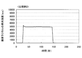
- 12 and 13 are graphs showing the results of measuring the emission intensity of oxygen radicals by optical emission spectroscopy (OES) in the steps of etching the silicon layers according to Comparative Example 1 and Comparative Example 2, respectively.
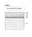
- 14 and 15 are diagrams schematically showing the state of the surface of the wafer W in the step of etching the silicon layer according to Comparative Example 1 and Comparative Example 2, respectively.
- the etching gas is turned into plasma in a state where the flow rate ratio of O 2 gas to SF 6 gas is set to a first flow rate ratio that is relatively large with respect to the second flow rate ratio. To do. Then, as shown in FIG. 12, the emission intensity of the oxygen radical O * becomes relatively high. This is considered because the deposition rate of the protective film 55 is higher than the etching rate of the protective film 55 and the protective film 55 is easily deposited on the surface of the mask film 54. At this time, as shown in FIG. 14, since the surface of the mask film 54 is covered with the protective film 55, the oxygen radical O * and the resist layer of the mask film 54 do not react. As a result, the mask film 54 made of a resist layer remains on the surface of the wafer W, and unreacted oxygen radicals O * existing in the plasma increase.
- the etching gas is turned into plasma in a state where the flow rate ratio of O 2 gas to SF 6 gas is set to a second flow rate ratio that is relatively small with respect to the first flow rate ratio. Then, as shown in FIG. 13, the emission intensity of the oxygen radical O * becomes relatively low. This is considered because the deposition rate of the protective film 55 is lower than the etching rate of the protective film 55 and the protective film 55 is difficult to deposit on the surface of the mask film 54.
- the oxygen radical O * reacts with the resist layer of the mask film 54. As a result, the mask film 54 made of a resist layer does not remain on the surface of the wafer W, and unreacted oxygen radicals O * existing in the plasma are reduced.
- the deposition rate of the protective film was measured when the flow rate ratio of O 2 gas to SiF 4 gas was changed.
- the result is shown in FIG.
- the horizontal axis of FIG. 16 shows the flow rate ratio of O 2 gas to SiF 4 gas
- the relative change in the flow rate ratio of O 2 gas to SF 6 gas is also shown indirectly.
- the deposition rate of the protective film is substantially uniform. To increase.
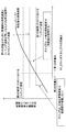
- FIG. 17 is a graph schematically showing the relationship between the flow rate ratio of O 2 gas to SF 6 gas and the deposition rate and etching rate of the protective film.
- the deposition rate of the protective film increases substantially uniformly as the flow rate ratio of O 2 gas to SF 6 gas increases.
- the etching rate of the protective film is considered to be less dependent on the flow rate ratio of O 2 gas to SF 6 gas, and therefore is represented by a substantially horizontal broken line in FIG.
- the flow rate ratio of O 2 gas to SF 6 gas is a predetermined flow rate ratio
- the deposition rate of the protective film and the etching rate become equal.
- the protective film When the flow ratio of O 2 gas to SF 6 gas is less than a predetermined flow ratio, the protective film is not deposited on the surface of the wafer and is etched. On the other hand, when the flow ratio of O 2 gas to SF 6 gas exceeds a predetermined flow ratio, a protective film is deposited on the surface of the wafer.
- the flow ratio of O 2 gas to SF 6 gas, the flow ratio of O 2 gas to SF 6 gas is not less than a predetermined flow rate ratio
- protection to the surface of the wafer Etching is performed in a state in which the film is deposited at a first flow rate ratio, and then the flow rate ratio is smaller than the first flow rate ratio, and the flow rate ratio of O 2 gas to SF 6 gas is a predetermined flow rate.
- the etching is performed in a state where the second flow rate ratio is such that the protective film is not deposited on the surface of the wafer and the surface of the wafer is etched.
- the deposition rate of the protective film is larger than the etching rate of the protective film, and the net deposition rate has a positive value. Therefore, the protective film is deposited on the surface of the resist layer and the sidewall of the hole. be able to. Further, as the etching progresses, the deposition rate of the protective film becomes smaller than the etching rate of the protective film, and the net deposition rate has a negative value. Therefore, the protective film is formed on the surface of the resist layer and the sidewall of the hole. Can be prevented from being deposited. Therefore, the diameter dimension of the hole portion gradually decreases along the depth direction of the hole portion, and the hole portion can be prevented from being tapered, and the side wall of the hole portion can be easily made perpendicular to the wafer surface. can do.
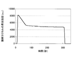
- FIG. 18 is a graph showing the result of measuring the emission intensity of oxygen radicals by OES in the step of etching the silicon layer according to Example 1 described above.
- the emission intensity of the oxygen radical O * is relatively large, then the emission intensity of the oxygen radical O * is decreased, and then the emission intensity of the oxygen radical O * .
- the flow rate ratio of O 2 gas to SF 6 gas is relatively large in step S1, the flow rate ratio decreases in step S2, and the flow rate ratio is relatively small in step S3. Therefore, in the present embodiment, the amount of unreacted oxygen radical O * is controlled by changing the flow ratio of O 2 gas to SF 6 gas.
- the first magnetic field is applied to the wafer.
- the first magnetic field etches the protective film by depositing the protective film by causing the plasma to react with the resist layer when the flow ratio of the O 2 gas to the SF 6 gas is the first flow ratio. It is larger than a predetermined magnetic field that makes the etching rate equal.
- the radius of rotation (Larmor radius) when electrons spirally move around the magnetic field lines decreases. That is, electrons existing near the wafer surface are always constrained to a region close to the wafer surface, so that the electron density near the wafer surface increases. Similarly, the plasma density near the wafer surface increases and the self-bias voltage decreases.
- the etching rate decreases.
- the flow rate ratio of the O 2 gas to the SF 6 gas when the deposition rate of the protective film and the etching rate are equal is reduced.
- the flow rate of O 2 gas for making the net deposition rate obtained by subtracting the etching rate from the deposition rate of the protective film a predetermined rate is near the wafer surface.
- the first magnetic field can be 215G, for example, and the second magnetic field can be 110G, for example.
- the first magnetic field is applied to the wafer, and the plasma is reacted with the resist layer in a state where the flow rate ratio of O 2 gas to SF 6 gas is the first flow rate ratio. Then, a protective film is deposited on the surface of the resist layer and the sidewall of the hole.
- the first magnetic field has a deposition rate for depositing a protective film on the surface of the resist layer and the sidewall of the hole, and etching for etching the protective film, when the flow rate ratio of O 2 gas to SF 6 gas is the first flow rate ratio. It is larger than a predetermined magnetic field that makes the speeds equal. Thereby, since the deposition rate of the protective film is higher than the etching rate of the protective film at the start of etching, the protective film can be deposited on the surface of the resist layer and the side wall of the hole to be formed.
- the plasma etching method with the progress of the etching, i.e., with increasing depth of the hole, while the flow rate of the SF 6 gas constant of O 2 gas Reduce the flow rate. Then, since the amount of oxygen radicals supplied into the hole portion is also reduced, the deposition rate at which the protective film is deposited can be reduced, and the etching rate can be made relatively higher than the deposition rate. Thereby, deposition of the protective film on the side wall of the hole can be suppressed. Therefore, the diameter of the hole is gradually reduced along the depth direction, and the hole can be more easily prevented from being tapered, and the side wall of the hole is more easily perpendicular to the surface of the wafer. Can be.
- the flow rate of O 2 gas for making the net deposition rate of the protective film a desired rate can be reduced by increasing the magnitude of the magnetic field applied to the wafer. Therefore, while adjusting the net deposition rate of the protective film to a desired rate, the amount of fluorine radical F * supplied into the hole can be substantially increased, and the etching rate for etching the hole can be increased. . Accordingly, the silicon layer can be etched at a higher speed.
- Example 1 described using Table 1, a net etching rate of 10.95 ⁇ m / min was obtained at the center of the wafer surface.
- Comparative Example 3 is performed under the same process conditions as Comparative Example 1 and the magnitude of the magnetic field applied to the wafer is 110 G, a net etching rate of 8.77 ⁇ m / min is obtained at the center of the wafer surface. It was. That is, it was confirmed that the etching rate in Example 1 was larger than the etching rate in Comparative Example 3. (Second Embodiment) Next, a plasma etching method according to the second embodiment of the present invention will be described.
- the same apparatus as the plasma etching apparatus according to the first embodiment can be used. Therefore, description of the etching apparatus according to this embodiment is omitted.
- the plasma etching method according to the present embodiment forms a through hole in a wafer using a TSV (Through-Silicon Via) technique in order to form a through electrode in a semiconductor device mounted three-dimensionally. . Therefore, the plasma etching method according to the present embodiment etches a bonded wafer in which a wafer for forming a through hole (hereinafter also referred to as “device wafer”) is bonded to a support wafer via an adhesive. This is different from the first embodiment.
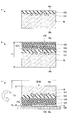
- 19 and 20 are cross-sectional views schematically showing the state of the wafer in each step of the semiconductor device manufacturing method including the plasma etching method according to the present embodiment.
- the bonded wafer has a device wafer W and a support wafer SW as shown in FIG.
- the device wafer W is a substrate on which a semiconductor device such as a transistor is formed on the surface Wa.
- the support wafer SW is a substrate for reinforcing the thinned device wafer W when the device wafer W is thinned by grinding the back surface Wb.
- the device wafer W is bonded to the support wafer SW via the adhesive G.
- the transistor 101 is formed on the surface of a device wafer W made of a silicon wafer or the like, and the interlayer insulating film 102 is formed on the device wafer W on which the transistor 101 is formed. (A in FIG. 19).
- a wiring structure 103 is formed on the interlayer insulating film 102.
- the wiring layers 104 and the insulating films 105 are alternately stacked, and via holes 106 that penetrate the insulating films 105 and electrically connect the upper and lower wiring layers 104 are formed (b in FIG. 19). ).
- the support wafer SW is a substrate that serves as a support to reinforce the thinned device wafer W and prevent warping when the device wafer W is thinned by grinding the back surface Wb, and is made of, for example, a silicon wafer or the like. .
- the bonded wafer is supported by, for example, a support portion provided in a grinding apparatus, the back surface Wb side of the wafer W is ground, and the thickness T1 before grinding is thinned to a predetermined thickness T2 (see FIG. 19 c).
- the predetermined thickness T2 can be set to, for example, 50 to 200 ⁇ m.
- the thickness of the interlayer insulating film 102 and the wiring structure 103 is exaggerated, but in actuality, the thickness of the interlayer insulating film 102 and the wiring structure 103 is It is extremely small compared to the thickness of the substrate itself of the wafer W (the same applies to FIG. 20).
- a resist pattern (not shown) is formed by applying a resist to the back surface Wb of the wafer W, exposing and developing the resist. Then, the same plasma etching process as in the first embodiment is performed, and the back surface Wb of the wafer W is etched to form the through hole V. Then, the resist remaining on the back surface Wb of the wafer W in which the through-hole V is formed is removed by ashing in the same manner as the plasma etching method according to the first embodiment (a in FIG. 20).
- the diameter of the through hole V can be set to 1 to 10 ⁇ m, for example.
- the depth of the through hole V corresponds to the thickness of the substrate itself of the wafer W after the back surface Wb of the wafer W is ground and thinned, and can be, for example, 50 to 200 ⁇ m.
- an insulating film 107 such as polyimide is formed so as to cover the inner peripheral surface of the through hole V, and the through electrode is formed in the through hole V whose inner peripheral surface is covered with the insulating film 107 by electrolytic plating or the like. 108 is formed (b in FIG. 20).
- the support wafer SW is peeled off from the wafer W to obtain a wafer W that is thinned and has the through electrodes 108 formed thereon.
- UV light ultraviolet light
- the adhesive force of the photoreactive adhesive G can be reduced and peeled off (c in FIG. 20).
- etching is performed with the flow rate ratio of O 2 gas to SF 6 gas set to the first flow rate ratio, and then this flow rate ratio is changed to the first flow rate ratio.
- Etching is performed in a state where the second flow rate ratio is smaller than the flow rate ratio.
- the deposition rate of the protective film becomes lower than the etching rate of the protective film, so that the protective film can be prevented from being deposited on the surface of the resist layer and the side walls of the through holes. Therefore, the diameter dimension of the through hole gradually decreases along the depth direction of the through hole, and it is possible to prevent the through hole from being tapered, and the side wall of the through hole can be easily made perpendicular to the wafer surface. can do.
- the first magnetic field is applied to the wafer in the plasma etching step shown in FIG.
- the first magnetic field etches the protective film by depositing the protective film by causing the plasma to react with the resist layer when the flow ratio of the O 2 gas to the SF 6 gas is the first flow ratio. It is larger than a predetermined magnetic field at which the etching rate becomes equal.
- step S1 to step S3 may be performed without applying a magnetic field.
Landscapes
- Physics & Mathematics (AREA)
- Engineering & Computer Science (AREA)
- Plasma & Fusion (AREA)
- Chemical & Material Sciences (AREA)
- Analytical Chemistry (AREA)
- Drying Of Semiconductors (AREA)
Abstract
Description
(第1の実施の形態)
始めに、本発明の第1の実施の形態に係るプラズマエッチング方法について説明する。
4F*+Si→SiF4 (1)
に示すように、フッ素ラジカルF*がSiと反応することによってSiF4が生成される。そして、生成されたSiF4が穴部51aの外へ排出されることにより、シリコン層51がエッチングされる。
O*+SiFx*→SiOFx (2)
に示すように、酸素ラジカルO*がフッ化シリコンのラジカルSiFx*と反応することによって、SiO系の保護膜55(例えばSiOFx)が堆積する。
P=I・V (3)
に示される。また、プラズマ電流Iはプラズマ密度に略比例すると考えられる。すると、供給される高周波電力Pが一定のとき、プラズマ密度の増加に伴って、プラズマ電流Iが増加し、自己バイアス電圧Vが減少する。
(第2の実施の形態)
次に、本発明の第2の実施の形態に係るプラズマエッチング方法について説明する。
2 サセプタ
4 支持部
15 第1の高周波電源
20 シャワーヘッド
23 エッチングガス供給部
24 ダイポールリング磁石
26 第2の高周波電源
35 SF6ガス源
36 O2ガス源
40 制御部
51 基体(シリコン層)
51a 穴部
51b 側壁
54 マスク膜(レジスト層)
55 保護膜
Claims (6)
- シリコン層と、前記シリコン層の上方に、所定のパターンにパターニングされたレジスト層とが形成された被処理基板が設置される処理容器内に、酸素ガスとフッ化硫黄ガスとを含んだエッチングガスを所定の流量で供給し、供給した前記エッチングガスから生成されたプラズマにより、前記レジスト層をマスクとして前記シリコン層をエッチングするプラズマエッチング方法であって、
フッ化硫黄ガスに対する酸素ガスの流量比を第1の流量比とした状態で、前記シリコン層をエッチングする第1のステップと、
前記流量比が前記第1の流量比から前記第1の流量比よりも小さい第2の流量比になるように、酸素ガスの流量を減少させながら前記シリコン層をエッチングする第2のステップと、
前記流量比を前記第2の流量比とした状態で、前記シリコン層をエッチングする第3のステップと
を有する、プラズマエッチング方法。 - 前記プラズマエッチング方法は、前記処理容器内で前記被処理基板を支持する支持部に第1の周波数を有する第1の高周波電力を供給した状態で、前記シリコン層をエッチングするものであり、
前記第1のステップは、
前記支持部に、前記第1の高周波電力を供給するとともに、前記第1の周波数よりも低い第2の周波数を有する第2の高周波電力を供給した状態で、前記シリコン層をエッチングする第4のステップと、
前記第4のステップの後、前記支持部への前記第2の高周波電力の供給を停止するとともに、前記支持部に前記第1の高周波電力を供給した状態で、前記シリコン層をエッチングする第5のステップと
を含む、請求項1に記載のプラズマエッチング方法。 - 前記第1のステップから前記第3のステップまでのすべてのステップにおいて、前記流量比を前記第1の流量比としたときに、前記エッチングガスから生成されたプラズマを前記レジスト層と反応させることで前記被処理基板の表面に保護膜を堆積させる堆積速度と、前記保護膜をエッチングするエッチング速度とが等しくなるような所定磁界よりも大きな第1の磁界を、前記被処理基板に印加した状態で、前記シリコン層をエッチングする、請求項1に記載のプラズマエッチング方法。
- 前記プラズマエッチング方法は、前記シリコン層をエッチングして穴部を形成するものであり、
前記第1のステップから前記第3のステップまでのすべてのステップにおいて、前記流量比を前記第1の流量比としたときに、前記エッチングガスから生成されたプラズマ中の酸素ラジカルを前記レジスト層と反応させることで前記レジスト層の表面及び形成される前記穴部の側壁に保護膜を堆積させる堆積速度と、前記保護膜をエッチングするエッチング速度とが等しくなるような所定磁界よりも大きな第1の磁界を、前記被処理基板に印加した状態で、前記シリコン層をエッチングするものである、請求項1に記載のプラズマエッチング方法。 - シリコン層と、前記シリコン層の上方に、所定のパターンにパターニングされたレジスト層とが形成された被処理基板が設置される処理容器内に、酸素ガスとフッ化硫黄ガスとを含んだエッチングガスを所定の流量で供給し、供給した前記エッチングガスから生成されたプラズマにより、前記レジスト層をマスクとして前記シリコン層をエッチングするプラズマエッチング方法であって、
エッチングを開始する際には、フッ化硫黄ガスに対する酸素ガスの流量比を第1の流量比としたときに、前記エッチングガスをプラズマ化したプラズマを前記レジスト層と反応させることで前記被処理基板の表面に保護膜を堆積させる堆積速度と、前記保護膜をエッチングするエッチング速度とが等しくなるような所定磁界よりも大きな第1の磁界を、前記被処理基板に印加するとともに、前記流量比を前記第1の流量比とした状態で、前記被処理基板の表面に前記保護膜を堆積するものであって、
エッチングの進行に伴って、前記被処理基板に前記第1の磁界を印加した状態で、酸素ガスの流量を減少させることによって、前記エッチング速度を前記堆積速度よりも相対的に大きくするものである、プラズマエッチング方法。 - シリコン層と、前記シリコン層の上方に、所定のパターンにパターニングされたレジスト層とが形成された被処理基板が設置される処理容器内に、酸素ガスとフッ化硫黄ガスとを含んだエッチングガスを所定の流量で供給し、供給した前記エッチングガスから生成されたプラズマにより、前記レジスト層をマスクとして前記シリコン層をエッチングして穴部を形成するプラズマエッチング方法であって、
エッチングを開始する際には、フッ化硫黄ガスに対する酸素ガスの流量比を第1の流量比としたときに、前記エッチングガスをプラズマ化して発生させた酸素ラジカルを前記レジスト層と反応させることで前記レジスト層の表面及び形成される前記穴部の側壁に保護膜を堆積させる堆積速度と、前記保護膜をエッチングするエッチング速度とが等しくなるような所定磁界よりも大きな第1の磁界を、前記被処理基板に印加するとともに、前記流量比を前記第1の流量比とした状態で、前記レジスト層の表面及び前記穴部の側壁に前記保護膜を堆積するものであって、
前記穴部の深さ寸法の増加に伴って、前記被処理基板に前記第1の磁界を印加した状態で、酸素ガスの流量を減少させることによって、前記エッチング速度を前記堆積速度よりも相対的に大きくするものである、プラズマエッチング方法。
Priority Applications (2)
| Application Number | Priority Date | Filing Date | Title |
|---|---|---|---|
| KR1020137032510A KR101888717B1 (ko) | 2011-06-15 | 2012-06-12 | 플라즈마 에칭 방법 |
| US14/125,363 US9048191B2 (en) | 2011-06-15 | 2012-06-12 | Plasma etching method |
Applications Claiming Priority (2)
| Application Number | Priority Date | Filing Date | Title |
|---|---|---|---|
| JP2011133482A JP5830275B2 (ja) | 2011-06-15 | 2011-06-15 | プラズマエッチング方法 |
| JP2011-133482 | 2011-06-15 |
Publications (1)
| Publication Number | Publication Date |
|---|---|
| WO2012173122A1 true WO2012173122A1 (ja) | 2012-12-20 |
Family
ID=47357109
Family Applications (1)
| Application Number | Title | Priority Date | Filing Date |
|---|---|---|---|
| PCT/JP2012/065034 Ceased WO2012173122A1 (ja) | 2011-06-15 | 2012-06-12 | プラズマエッチング方法 |
Country Status (5)
| Country | Link |
|---|---|
| US (1) | US9048191B2 (ja) |
| JP (1) | JP5830275B2 (ja) |
| KR (1) | KR101888717B1 (ja) |
| TW (1) | TWI450332B (ja) |
| WO (1) | WO2012173122A1 (ja) |
Cited By (2)
| Publication number | Priority date | Publication date | Assignee | Title |
|---|---|---|---|---|
| US20150192702A1 (en) * | 2012-11-16 | 2015-07-09 | Nalux Co., Ltd. | Mold, optical element and method for manufacturing the same |
| TWI739341B (zh) * | 2020-03-12 | 2021-09-11 | 馗鼎奈米科技股份有限公司 | 電漿蝕刻設備 |
Families Citing this family (13)
| Publication number | Priority date | Publication date | Assignee | Title |
|---|---|---|---|---|
| US9336998B2 (en) * | 2014-05-09 | 2016-05-10 | Varian Semiconductor Equipment Associates, Inc. | Apparatus and method for dynamic control of ion beam energy and angle |
| CN105097406B (zh) * | 2015-06-11 | 2017-06-09 | 京东方科技集团股份有限公司 | 平滑装置、平滑方法、薄膜晶体管、显示基板及显示装置 |
| US9711359B2 (en) * | 2015-08-13 | 2017-07-18 | Lam Research Corporation | Shadow trim line edge roughness reduction |
| JP6859088B2 (ja) * | 2016-12-14 | 2021-04-14 | エイブリック株式会社 | 半導体装置の製造方法 |
| JP6832171B2 (ja) | 2017-01-24 | 2021-02-24 | 東京エレクトロン株式会社 | プラズマ処理装置のチャンバ本体の内部のクリーニングを含むプラズマ処理方法 |
| JP2018170363A (ja) * | 2017-03-29 | 2018-11-01 | 東芝メモリ株式会社 | 半導体装置の製造方法及び半導体装置 |
| JP6928548B2 (ja) * | 2017-12-27 | 2021-09-01 | 東京エレクトロン株式会社 | エッチング方法 |
| CN108321101B (zh) * | 2018-02-24 | 2020-09-11 | 惠科股份有限公司 | 一种电极组件和蚀刻设备 |
| JP7110034B2 (ja) * | 2018-08-24 | 2022-08-01 | 東京エレクトロン株式会社 | エッチングする方法及びプラズマ処理装置 |
| JP2020203817A (ja) * | 2019-06-19 | 2020-12-24 | 株式会社アルバック | シリコンナノチューブの製造方法 |
| JP7357513B2 (ja) * | 2019-11-12 | 2023-10-06 | 東京エレクトロン株式会社 | プラズマ処理装置 |
| CN114639602B (zh) * | 2020-12-15 | 2026-03-27 | 东京毅力科创株式会社 | 蚀刻方法和蚀刻装置 |
| CN115321471B (zh) * | 2022-08-12 | 2025-01-17 | 合肥英仕博精密装备有限公司 | 一种干法刻蚀聚酰亚胺牺牲层的方法 |
Citations (5)
| Publication number | Priority date | Publication date | Assignee | Title |
|---|---|---|---|---|
| JP2006278498A (ja) * | 2005-03-28 | 2006-10-12 | Tokyo Electron Ltd | プラズマエッチング方法及びその装置 |
| JP2007227829A (ja) * | 2006-02-27 | 2007-09-06 | Tokyo Electron Ltd | プラズマエッチング装置およびプラズマエッチング方法 |
| JP2008300870A (ja) * | 2008-08-18 | 2008-12-11 | Oki Data Corp | 半導体装置の製造方法、および半導体製造装置 |
| JP2009267432A (ja) * | 2009-06-29 | 2009-11-12 | Elpida Memory Inc | 半導体集積回路装置の製造方法 |
| JP2010098220A (ja) * | 2008-10-20 | 2010-04-30 | Tokyo Electron Ltd | プラズマエッチング方法及びプラズマエッチング装置 |
Family Cites Families (7)
| Publication number | Priority date | Publication date | Assignee | Title |
|---|---|---|---|---|
| JP2004087738A (ja) * | 2002-08-26 | 2004-03-18 | Tokyo Electron Ltd | Siエッチング方法 |
| JP2004128063A (ja) * | 2002-09-30 | 2004-04-22 | Toshiba Corp | 半導体装置及びその製造方法 |
| US20060090773A1 (en) * | 2004-11-04 | 2006-05-04 | Applied Materials, Inc. | Sulfur hexafluoride remote plasma source clean |
| JP4371999B2 (ja) * | 2004-12-28 | 2009-11-25 | パナソニック株式会社 | ドライエッチング方法及びドライエッチング装置 |
| US7442274B2 (en) * | 2005-03-28 | 2008-10-28 | Tokyo Electron Limited | Plasma etching method and apparatus therefor |
| US20070202701A1 (en) * | 2006-02-27 | 2007-08-30 | Tokyo Electron Limited | Plasma etching apparatus and method |
| JP5102653B2 (ja) | 2008-02-29 | 2012-12-19 | 東京エレクトロン株式会社 | プラズマエッチング方法、プラズマエッチング装置及びコンピュータ記憶媒体 |
-
2011
- 2011-06-15 JP JP2011133482A patent/JP5830275B2/ja active Active
-
2012
- 2012-06-08 TW TW101120738A patent/TWI450332B/zh active
- 2012-06-12 KR KR1020137032510A patent/KR101888717B1/ko active Active
- 2012-06-12 WO PCT/JP2012/065034 patent/WO2012173122A1/ja not_active Ceased
- 2012-06-12 US US14/125,363 patent/US9048191B2/en active Active
Patent Citations (5)
| Publication number | Priority date | Publication date | Assignee | Title |
|---|---|---|---|---|
| JP2006278498A (ja) * | 2005-03-28 | 2006-10-12 | Tokyo Electron Ltd | プラズマエッチング方法及びその装置 |
| JP2007227829A (ja) * | 2006-02-27 | 2007-09-06 | Tokyo Electron Ltd | プラズマエッチング装置およびプラズマエッチング方法 |
| JP2008300870A (ja) * | 2008-08-18 | 2008-12-11 | Oki Data Corp | 半導体装置の製造方法、および半導体製造装置 |
| JP2010098220A (ja) * | 2008-10-20 | 2010-04-30 | Tokyo Electron Ltd | プラズマエッチング方法及びプラズマエッチング装置 |
| JP2009267432A (ja) * | 2009-06-29 | 2009-11-12 | Elpida Memory Inc | 半導体集積回路装置の製造方法 |
Cited By (3)
| Publication number | Priority date | Publication date | Assignee | Title |
|---|---|---|---|---|
| US20150192702A1 (en) * | 2012-11-16 | 2015-07-09 | Nalux Co., Ltd. | Mold, optical element and method for manufacturing the same |
| US10353119B2 (en) | 2012-11-16 | 2019-07-16 | Nalux Co., Ltd. | Method for manufacturing mold or optical element |
| TWI739341B (zh) * | 2020-03-12 | 2021-09-11 | 馗鼎奈米科技股份有限公司 | 電漿蝕刻設備 |
Also Published As
| Publication number | Publication date |
|---|---|
| TWI450332B (zh) | 2014-08-21 |
| TW201314766A (zh) | 2013-04-01 |
| KR20140036217A (ko) | 2014-03-25 |
| JP5830275B2 (ja) | 2015-12-09 |
| US9048191B2 (en) | 2015-06-02 |
| KR101888717B1 (ko) | 2018-08-14 |
| US20140113450A1 (en) | 2014-04-24 |
| JP2013004679A (ja) | 2013-01-07 |
Similar Documents
| Publication | Publication Date | Title |
|---|---|---|
| JP5830275B2 (ja) | プラズマエッチング方法 | |
| JP5981106B2 (ja) | プラズマエッチング方法 | |
| JP6001529B2 (ja) | プラズマエッチング装置及びプラズマエッチング方法 | |
| US9324569B2 (en) | Plasma etching method and plasma etching apparatus | |
| KR102080246B1 (ko) | 패턴 형성 방법 및 기판 처리 시스템 | |
| KR101384589B1 (ko) | 반도체 장치의 제조 방법 | |
| US20140227876A1 (en) | Semiconductor device manufacturing method | |
| US9607811B2 (en) | Workpiece processing method | |
| JP6298391B2 (ja) | プラズマ処理方法及びプラズマ処理装置 | |
| JP6017928B2 (ja) | プラズマエッチング方法及びプラズマエッチング装置 | |
| US7902078B2 (en) | Processing method and plasma etching method | |
| US9034772B2 (en) | Etching method | |
| JP6529943B2 (ja) | 半導体素子の製造方法及びその製造方法に用いられるプラズマエッチング装置 | |
| JP5047644B2 (ja) | プラズマエッチング方法、プラズマエッチング装置、制御プログラム及びコンピュータ記憶媒体 | |
| US9156307B2 (en) | Plasma etching method and plasma etching apparatus |
Legal Events
| Date | Code | Title | Description |
|---|---|---|---|
| 121 | Ep: the epo has been informed by wipo that ep was designated in this application |
Ref document number: 12800333 Country of ref document: EP Kind code of ref document: A1 |
|
| ENP | Entry into the national phase |
Ref document number: 20137032510 Country of ref document: KR Kind code of ref document: A |
|
| WWE | Wipo information: entry into national phase |
Ref document number: 14125363 Country of ref document: US |
|
| NENP | Non-entry into the national phase |
Ref country code: DE |
|
| 122 | Ep: pct application non-entry in european phase |
Ref document number: 12800333 Country of ref document: EP Kind code of ref document: A1 |