WO2012172965A1 - Dispositif à semi-conducteur en carbure de silicium et son procédé de fabrication - Google Patents
Dispositif à semi-conducteur en carbure de silicium et son procédé de fabrication Download PDFInfo
- Publication number
- WO2012172965A1 WO2012172965A1 PCT/JP2012/063722 JP2012063722W WO2012172965A1 WO 2012172965 A1 WO2012172965 A1 WO 2012172965A1 JP 2012063722 W JP2012063722 W JP 2012063722W WO 2012172965 A1 WO2012172965 A1 WO 2012172965A1
- Authority
- WO
- WIPO (PCT)
- Prior art keywords
- silicon carbide
- insulating film
- film
- gate
- gate electrode
- Prior art date
Links
- HBMJWWWQQXIZIP-UHFFFAOYSA-N silicon carbide Chemical compound [Si+]#[C-] HBMJWWWQQXIZIP-UHFFFAOYSA-N 0.000 title claims abstract description 114
- 229910010271 silicon carbide Inorganic materials 0.000 title claims abstract description 114
- 239000004065 semiconductor Substances 0.000 title claims description 45
- 238000004519 manufacturing process Methods 0.000 title claims description 24
- 238000000034 method Methods 0.000 title claims description 19
- 239000000758 substrate Substances 0.000 claims abstract description 80
- 229910052751 metal Inorganic materials 0.000 claims abstract description 31
- 239000002184 metal Substances 0.000 claims abstract description 31
- 229910021420 polycrystalline silicon Inorganic materials 0.000 claims abstract description 29
- 229920005591 polysilicon Polymers 0.000 claims abstract description 29
- 239000011229 interlayer Substances 0.000 claims abstract description 25
- 230000004888 barrier function Effects 0.000 claims abstract description 20
- 230000008018 melting Effects 0.000 claims abstract description 9
- 238000002844 melting Methods 0.000 claims abstract description 9
- 238000010438 heat treatment Methods 0.000 claims description 21
- 239000000463 material Substances 0.000 claims description 17
- 239000003870 refractory metal Substances 0.000 claims description 9
- 238000000059 patterning Methods 0.000 claims description 5
- 239000004020 conductor Substances 0.000 claims description 4
- 239000010410 layer Substances 0.000 description 24
- 210000000746 body region Anatomy 0.000 description 17
- 239000012535 impurity Substances 0.000 description 16
- 239000013078 crystal Substances 0.000 description 15
- 238000005468 ion implantation Methods 0.000 description 9
- MWUXSHHQAYIFBG-UHFFFAOYSA-N Nitric oxide Chemical compound O=[N] MWUXSHHQAYIFBG-UHFFFAOYSA-N 0.000 description 6
- VYPSYNLAJGMNEJ-UHFFFAOYSA-N Silicium dioxide Chemical compound O=[Si]=O VYPSYNLAJGMNEJ-UHFFFAOYSA-N 0.000 description 6
- 229910052782 aluminium Inorganic materials 0.000 description 6
- XAGFODPZIPBFFR-UHFFFAOYSA-N aluminium Chemical compound [Al] XAGFODPZIPBFFR-UHFFFAOYSA-N 0.000 description 6
- PXHVJJICTQNCMI-UHFFFAOYSA-N nickel Substances [Ni] PXHVJJICTQNCMI-UHFFFAOYSA-N 0.000 description 6
- XKRFYHLGVUSROY-UHFFFAOYSA-N Argon Chemical compound [Ar] XKRFYHLGVUSROY-UHFFFAOYSA-N 0.000 description 4
- 238000005229 chemical vapour deposition Methods 0.000 description 4
- 238000005530 etching Methods 0.000 description 4
- 239000007789 gas Substances 0.000 description 4
- 238000000206 photolithography Methods 0.000 description 4
- 229910004298 SiO 2 Inorganic materials 0.000 description 3
- 230000015572 biosynthetic process Effects 0.000 description 3
- 150000002500 ions Chemical class 0.000 description 3
- 125000004433 nitrogen atom Chemical group N* 0.000 description 3
- 235000012239 silicon dioxide Nutrition 0.000 description 3
- 239000000377 silicon dioxide Substances 0.000 description 3
- IJGRMHOSHXDMSA-UHFFFAOYSA-N Atomic nitrogen Chemical compound N#N IJGRMHOSHXDMSA-UHFFFAOYSA-N 0.000 description 2
- OKTJSMMVPCPJKN-UHFFFAOYSA-N Carbon Chemical compound [C] OKTJSMMVPCPJKN-UHFFFAOYSA-N 0.000 description 2
- 230000004913 activation Effects 0.000 description 2
- 229910045601 alloy Inorganic materials 0.000 description 2
- 239000000956 alloy Substances 0.000 description 2
- 229910052786 argon Inorganic materials 0.000 description 2
- 229910052799 carbon Inorganic materials 0.000 description 2
- 230000005669 field effect Effects 0.000 description 2
- 230000004048 modification Effects 0.000 description 2
- 238000012986 modification Methods 0.000 description 2
- 229910052759 nickel Inorganic materials 0.000 description 2
- 229910021334 nickel silicide Inorganic materials 0.000 description 2
- RUFLMLWJRZAWLJ-UHFFFAOYSA-N nickel silicide Chemical compound [Ni]=[Si]=[Ni] RUFLMLWJRZAWLJ-UHFFFAOYSA-N 0.000 description 2
- 229910021332 silicide Inorganic materials 0.000 description 2
- FVBUAEGBCNSCDD-UHFFFAOYSA-N silicide(4-) Chemical compound [Si-4] FVBUAEGBCNSCDD-UHFFFAOYSA-N 0.000 description 2
- 239000010936 titanium Substances 0.000 description 2
- 238000007740 vapor deposition Methods 0.000 description 2
- ZOXJGFHDIHLPTG-UHFFFAOYSA-N Boron Chemical compound [B] ZOXJGFHDIHLPTG-UHFFFAOYSA-N 0.000 description 1
- OAICVXFJPJFONN-UHFFFAOYSA-N Phosphorus Chemical compound [P] OAICVXFJPJFONN-UHFFFAOYSA-N 0.000 description 1
- RTAQQCXQSZGOHL-UHFFFAOYSA-N Titanium Chemical compound [Ti] RTAQQCXQSZGOHL-UHFFFAOYSA-N 0.000 description 1
- NRTOMJZYCJJWKI-UHFFFAOYSA-N Titanium nitride Chemical compound [Ti]#N NRTOMJZYCJJWKI-UHFFFAOYSA-N 0.000 description 1
- QVGXLLKOCUKJST-UHFFFAOYSA-N atomic oxygen Chemical compound [O] QVGXLLKOCUKJST-UHFFFAOYSA-N 0.000 description 1
- IVHJCRXBQPGLOV-UHFFFAOYSA-N azanylidynetungsten Chemical compound [W]#N IVHJCRXBQPGLOV-UHFFFAOYSA-N 0.000 description 1
- 229910052796 boron Inorganic materials 0.000 description 1
- 229910052802 copper Inorganic materials 0.000 description 1
- 230000005684 electric field Effects 0.000 description 1
- 229910052737 gold Inorganic materials 0.000 description 1
- 239000011261 inert gas Substances 0.000 description 1
- 239000012212 insulator Substances 0.000 description 1
- 229910044991 metal oxide Inorganic materials 0.000 description 1
- 150000004706 metal oxides Chemical class 0.000 description 1
- 229910052750 molybdenum Inorganic materials 0.000 description 1
- 229910052757 nitrogen Inorganic materials 0.000 description 1
- 239000001301 oxygen Substances 0.000 description 1
- 229910052760 oxygen Inorganic materials 0.000 description 1
- 229910052698 phosphorus Inorganic materials 0.000 description 1
- 239000011574 phosphorus Substances 0.000 description 1
- 230000002040 relaxant effect Effects 0.000 description 1
- 229910052710 silicon Inorganic materials 0.000 description 1
- 239000002356 single layer Substances 0.000 description 1
- 229910052715 tantalum Inorganic materials 0.000 description 1
- MZLGASXMSKOWSE-UHFFFAOYSA-N tantalum nitride Chemical compound [Ta]#N MZLGASXMSKOWSE-UHFFFAOYSA-N 0.000 description 1
- 229910052719 titanium Inorganic materials 0.000 description 1
- MAKDTFFYCIMFQP-UHFFFAOYSA-N titanium tungsten Chemical compound [Ti].[W] MAKDTFFYCIMFQP-UHFFFAOYSA-N 0.000 description 1
- 229910052721 tungsten Inorganic materials 0.000 description 1
Images


Classifications
-
- H—ELECTRICITY
- H01—ELECTRIC ELEMENTS
- H01L—SEMICONDUCTOR DEVICES NOT COVERED BY CLASS H10
- H01L29/00—Semiconductor devices adapted for rectifying, amplifying, oscillating or switching, or capacitors or resistors with at least one potential-jump barrier or surface barrier, e.g. PN junction depletion layer or carrier concentration layer; Details of semiconductor bodies or of electrodes thereof ; Multistep manufacturing processes therefor
- H01L29/66—Types of semiconductor device ; Multistep manufacturing processes therefor
- H01L29/68—Types of semiconductor device ; Multistep manufacturing processes therefor controllable by only the electric current supplied, or only the electric potential applied, to an electrode which does not carry the current to be rectified, amplified or switched
- H01L29/76—Unipolar devices, e.g. field effect transistors
- H01L29/772—Field effect transistors
- H01L29/78—Field effect transistors with field effect produced by an insulated gate
- H01L29/7801—DMOS transistors, i.e. MISFETs with a channel accommodating body or base region adjoining a drain drift region
- H01L29/7802—Vertical DMOS transistors, i.e. VDMOS transistors
-
- H—ELECTRICITY
- H01—ELECTRIC ELEMENTS
- H01L—SEMICONDUCTOR DEVICES NOT COVERED BY CLASS H10
- H01L29/00—Semiconductor devices adapted for rectifying, amplifying, oscillating or switching, or capacitors or resistors with at least one potential-jump barrier or surface barrier, e.g. PN junction depletion layer or carrier concentration layer; Details of semiconductor bodies or of electrodes thereof ; Multistep manufacturing processes therefor
- H01L29/02—Semiconductor bodies ; Multistep manufacturing processes therefor
- H01L29/12—Semiconductor bodies ; Multistep manufacturing processes therefor characterised by the materials of which they are formed
- H01L29/16—Semiconductor bodies ; Multistep manufacturing processes therefor characterised by the materials of which they are formed including, apart from doping materials or other impurities, only elements of Group IV of the Periodic System
- H01L29/1608—Silicon carbide
-
- H—ELECTRICITY
- H01—ELECTRIC ELEMENTS
- H01L—SEMICONDUCTOR DEVICES NOT COVERED BY CLASS H10
- H01L29/00—Semiconductor devices adapted for rectifying, amplifying, oscillating or switching, or capacitors or resistors with at least one potential-jump barrier or surface barrier, e.g. PN junction depletion layer or carrier concentration layer; Details of semiconductor bodies or of electrodes thereof ; Multistep manufacturing processes therefor
- H01L29/40—Electrodes ; Multistep manufacturing processes therefor
- H01L29/43—Electrodes ; Multistep manufacturing processes therefor characterised by the materials of which they are formed
- H01L29/49—Metal-insulator-semiconductor electrodes, e.g. gates of MOSFET
- H01L29/4916—Metal-insulator-semiconductor electrodes, e.g. gates of MOSFET the conductor material next to the insulator being a silicon layer, e.g. polysilicon doped with boron, phosphorus or nitrogen
- H01L29/4925—Metal-insulator-semiconductor electrodes, e.g. gates of MOSFET the conductor material next to the insulator being a silicon layer, e.g. polysilicon doped with boron, phosphorus or nitrogen with a multiple layer structure, e.g. several silicon layers with different crystal structure or grain arrangement
- H01L29/4941—Metal-insulator-semiconductor electrodes, e.g. gates of MOSFET the conductor material next to the insulator being a silicon layer, e.g. polysilicon doped with boron, phosphorus or nitrogen with a multiple layer structure, e.g. several silicon layers with different crystal structure or grain arrangement with a barrier layer between the silicon and the metal or metal silicide upper layer, e.g. Silicide/TiN/Polysilicon
-
- H—ELECTRICITY
- H01—ELECTRIC ELEMENTS
- H01L—SEMICONDUCTOR DEVICES NOT COVERED BY CLASS H10
- H01L29/00—Semiconductor devices adapted for rectifying, amplifying, oscillating or switching, or capacitors or resistors with at least one potential-jump barrier or surface barrier, e.g. PN junction depletion layer or carrier concentration layer; Details of semiconductor bodies or of electrodes thereof ; Multistep manufacturing processes therefor
- H01L29/66—Types of semiconductor device ; Multistep manufacturing processes therefor
- H01L29/66007—Multistep manufacturing processes
- H01L29/66075—Multistep manufacturing processes of devices having semiconductor bodies comprising group 14 or group 13/15 materials
- H01L29/66227—Multistep manufacturing processes of devices having semiconductor bodies comprising group 14 or group 13/15 materials the devices being controllable only by the electric current supplied or the electric potential applied, to an electrode which does not carry the current to be rectified, amplified or switched, e.g. three-terminal devices
- H01L29/66409—Unipolar field-effect transistors
- H01L29/66477—Unipolar field-effect transistors with an insulated gate, i.e. MISFET
- H01L29/66674—DMOS transistors, i.e. MISFETs with a channel accommodating body or base region adjoining a drain drift region
- H01L29/66712—Vertical DMOS transistors, i.e. VDMOS transistors
-
- H—ELECTRICITY
- H01—ELECTRIC ELEMENTS
- H01L—SEMICONDUCTOR DEVICES NOT COVERED BY CLASS H10
- H01L29/00—Semiconductor devices adapted for rectifying, amplifying, oscillating or switching, or capacitors or resistors with at least one potential-jump barrier or surface barrier, e.g. PN junction depletion layer or carrier concentration layer; Details of semiconductor bodies or of electrodes thereof ; Multistep manufacturing processes therefor
- H01L29/66—Types of semiconductor device ; Multistep manufacturing processes therefor
- H01L29/68—Types of semiconductor device ; Multistep manufacturing processes therefor controllable by only the electric current supplied, or only the electric potential applied, to an electrode which does not carry the current to be rectified, amplified or switched
- H01L29/76—Unipolar devices, e.g. field effect transistors
- H01L29/772—Field effect transistors
- H01L29/78—Field effect transistors with field effect produced by an insulated gate
- H01L29/7801—DMOS transistors, i.e. MISFETs with a channel accommodating body or base region adjoining a drain drift region
- H01L29/7802—Vertical DMOS transistors, i.e. VDMOS transistors
- H01L29/7811—Vertical DMOS transistors, i.e. VDMOS transistors with an edge termination structure
-
- H—ELECTRICITY
- H01—ELECTRIC ELEMENTS
- H01L—SEMICONDUCTOR DEVICES NOT COVERED BY CLASS H10
- H01L29/00—Semiconductor devices adapted for rectifying, amplifying, oscillating or switching, or capacitors or resistors with at least one potential-jump barrier or surface barrier, e.g. PN junction depletion layer or carrier concentration layer; Details of semiconductor bodies or of electrodes thereof ; Multistep manufacturing processes therefor
- H01L29/66—Types of semiconductor device ; Multistep manufacturing processes therefor
- H01L29/68—Types of semiconductor device ; Multistep manufacturing processes therefor controllable by only the electric current supplied, or only the electric potential applied, to an electrode which does not carry the current to be rectified, amplified or switched
- H01L29/76—Unipolar devices, e.g. field effect transistors
- H01L29/772—Field effect transistors
- H01L29/78—Field effect transistors with field effect produced by an insulated gate
- H01L29/7801—DMOS transistors, i.e. MISFETs with a channel accommodating body or base region adjoining a drain drift region
- H01L29/7802—Vertical DMOS transistors, i.e. VDMOS transistors
- H01L29/7813—Vertical DMOS transistors, i.e. VDMOS transistors with trench gate electrode, e.g. UMOS transistors
-
- H—ELECTRICITY
- H01—ELECTRIC ELEMENTS
- H01L—SEMICONDUCTOR DEVICES NOT COVERED BY CLASS H10
- H01L29/00—Semiconductor devices adapted for rectifying, amplifying, oscillating or switching, or capacitors or resistors with at least one potential-jump barrier or surface barrier, e.g. PN junction depletion layer or carrier concentration layer; Details of semiconductor bodies or of electrodes thereof ; Multistep manufacturing processes therefor
- H01L29/02—Semiconductor bodies ; Multistep manufacturing processes therefor
- H01L29/06—Semiconductor bodies ; Multistep manufacturing processes therefor characterised by their shape; characterised by the shapes, relative sizes, or dispositions of the semiconductor regions ; characterised by the concentration or distribution of impurities within semiconductor regions
- H01L29/08—Semiconductor bodies ; Multistep manufacturing processes therefor characterised by their shape; characterised by the shapes, relative sizes, or dispositions of the semiconductor regions ; characterised by the concentration or distribution of impurities within semiconductor regions with semiconductor regions connected to an electrode carrying current to be rectified, amplified or switched and such electrode being part of a semiconductor device which comprises three or more electrodes
- H01L29/0843—Source or drain regions of field-effect devices
- H01L29/0847—Source or drain regions of field-effect devices of field-effect transistors with insulated gate
- H01L29/0852—Source or drain regions of field-effect devices of field-effect transistors with insulated gate of DMOS transistors
- H01L29/0873—Drain regions
- H01L29/0878—Impurity concentration or distribution
-
- H—ELECTRICITY
- H01—ELECTRIC ELEMENTS
- H01L—SEMICONDUCTOR DEVICES NOT COVERED BY CLASS H10
- H01L29/00—Semiconductor devices adapted for rectifying, amplifying, oscillating or switching, or capacitors or resistors with at least one potential-jump barrier or surface barrier, e.g. PN junction depletion layer or carrier concentration layer; Details of semiconductor bodies or of electrodes thereof ; Multistep manufacturing processes therefor
- H01L29/40—Electrodes ; Multistep manufacturing processes therefor
- H01L29/43—Electrodes ; Multistep manufacturing processes therefor characterised by the materials of which they are formed
- H01L29/45—Ohmic electrodes
Definitions
- the present invention relates to a silicon carbide semiconductor device and a method of manufacturing the same, and more particularly to a silicon carbide semiconductor device having a gate electrode and a method of manufacturing the same.
- Patent Document 1 JP-A-2010-171417 discloses a MOSFET (Metal Oxide Semiconductor Field Effect Transistor) having a silicon carbide substrate, a gate pad, and a gate electrode.
- the gate electrode is made of polysilicon.
- the present invention has been made to address such a problem, and it is an object of the present invention to provide a silicon carbide semiconductor device capable of suppressing the electrical resistance of a gate electrode and a method of manufacturing the same.
- the silicon carbide semiconductor device of the present invention has a silicon carbide substrate, a gate insulating film, a gate electrode, an interlayer insulating film, and a wiring.
- the gate insulating film is provided on a silicon carbide substrate.
- the gate electrode is provided on the gate insulating film.
- the gate electrode includes a polysilicon film in contact with the gate insulating film, a barrier film provided on the polysilicon film, and a metal film provided on the barrier film and made of a high melting point metal.
- the interlayer insulating film is arranged to cover the gate insulating film and the gate electrode provided on the gate insulating film.
- the interlayer insulating film has a substrate contact hole that partially exposes the silicon carbide substrate in a region in contact with the gate insulating film.
- the wiring is electrically connected to the silicon carbide substrate through the substrate contact hole, and is electrically isolated from the gate electrode by the interlayer insulating film.
- the gate electrode since the gate electrode includes the refractory metal film having a lower resistivity than the polysilicon film, compared to the case where the gate electrode is formed of only the polysilicon film, The electrical resistance of the gate electrode can be suppressed.
- the interlayer insulating film has a gate contact hole partially exposing the gate electrode.
- the silicon carbide semiconductor device has a gate pad electrically connected to the gate electrode through the gate contact hole.
- a current path from the gate pad can be formed by the gate electrode having a small electric resistance.
- the wiring and the gate pad are made of the same material. Thereby, the silicon carbide semiconductor device can be manufactured more easily than when the material of the wiring and the material of the gate pad are different.
- the refractory metal has a melting point above 1000 ° C.
- the heat treatment can be performed at a temperature higher than 1000.degree.
- the silicon carbide substrate may be provided with a trench, and at least a part of the gate electrode may be disposed in the trench. Thereby, the electrical resistance of the gate electrode can be further suppressed.
- the method for manufacturing a silicon carbide semiconductor device of the present invention has the following steps.
- a gate insulating film is formed on the silicon carbide substrate.
- a gate electrode is formed on the gate insulating film.
- the step of forming the gate electrode the step of forming a polysilicon film in contact with the gate insulating film, the step of forming a barrier film on the polysilicon film, and the step of forming a metal film made of refractory metal on the barrier film
- the step of An interlayer insulating film is formed to cover the gate insulating film and the gate electrode provided on the gate insulating film, and has a substrate contact hole that partially exposes the silicon carbide substrate in a region in contact with the gate insulating film.
- An interconnection electrically connected to the silicon carbide substrate through the substrate contact hole and electrically insulated from the gate electrode by the interlayer insulating film is formed.
- the gate electrode since the gate electrode includes a refractory metal film having a resistivity lower than that of the polysilicon film, the gate electrode is formed of only the polysilicon film. Thus, the electrical resistance of the gate electrode can be suppressed.
- the silicon carbide substrate is heat-treated to make the electrical connection between the wiring and the silicon carbide substrate more ohmic.
- the electrical connection between the wiring and the silicon carbide substrate can be made more ohmic.
- the step of heat-treating the silicon carbide substrate includes the step of heating the silicon carbide substrate to a temperature exceeding 1000 ° C. Thereby, the electrical connection between the wiring and the silicon carbide substrate can be made more ohmic.
- the step of forming the wiring includes the steps of forming a conductor film in contact with each of the gate electrode and the silicon carbide substrate, and patterning the conductor film.
- the patterning process By the patterning process, a wire and a gate pad provided on part of the gate electrode are formed.
- the silicon carbide semiconductor device can be manufactured more easily than when the wiring and the gate pad are separately formed.
- a trench may be formed in the silicon carbide substrate, and at least a portion of the gate electrode may be disposed in the trench. Thereby, the electrical resistance of the gate electrode can be further suppressed.
- the electrical resistance can be suppressed.
- FIG. 1 is a plan view schematically showing a structure of a silicon carbide semiconductor device in a first embodiment.
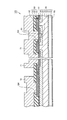
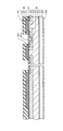
- FIG. 2 is a schematic cross-sectional view taken along line II-II of FIG.
- FIG. 3 is a cross sectional view schematically showing a first step of a method of manufacturing the silicon carbide semiconductor device of FIG. 1 in a view corresponding to the view of FIG. 2.
- FIG. 3 is a cross sectional view schematically showing a second step of the method for manufacturing the silicon carbide semiconductor device of FIG. 1 in a view corresponding to the view of FIG. 2.
- FIG. 13 is a cross sectional view schematically showing a third step of the method for manufacturing the silicon carbide semiconductor device of FIG. 1 in a view corresponding to the view of FIG. 2.
- FIG. 1 is a plan view schematically showing a structure of a silicon carbide semiconductor device in a first embodiment.
- FIG. 2 is a schematic cross-sectional view taken along line II-II of FIG.
- FIG. 3 is
- FIG. 14 is a cross sectional view schematically showing a fourth step of the method for manufacturing the silicon carbide semiconductor device of FIG. 1 in a view corresponding to the view of FIG. 2.
- FIG. 13 is a cross sectional view schematically showing a fifth step of the method for manufacturing the silicon carbide semiconductor device of FIG. 1 in a view corresponding to the view of FIG. 2.
- FIG. 13 is a cross sectional view schematically showing a sixth step of the method for manufacturing the silicon carbide semiconductor device of FIG. 1 in a view corresponding to the view of FIG. 2.
- FIG. 13 is a cross sectional view schematically showing a seventh step of the method for manufacturing the silicon carbide semiconductor device of FIG. 1 in a view corresponding to the view of FIG. 2.
- FIG. 13 is a cross sectional view schematically showing a eighth step of the method for manufacturing the silicon carbide semiconductor device of FIG. 1 in a view corresponding to the view of FIG. 2.
- FIG. 13 is a cross sectional view schematically showing a ninth step of the method for manufacturing the silicon carbide semiconductor device of FIG. 1 in a view corresponding to the view of FIG. 2.
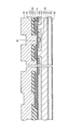
- FIG. 3 is a cross sectional view schematically showing a structure of a silicon carbide semiconductor device in a second embodiment in a view corresponding to the view in FIG. 2.
- FIG. 13 is a cross sectional view schematically showing a first step of a method of manufacturing the silicon carbide semiconductor device of FIG. 12 in a view corresponding to the view of FIG. 12.
- FIG. 13 is a cross sectional view schematically showing a second step of the method for manufacturing the silicon carbide semiconductor device of FIG. 12 in a view corresponding to the view of FIG. 12. It is sectional drawing which shows roughly the modification of the structure of FIG.
- the silicon carbide semiconductor device of the present embodiment is a MOSFET 101, more specifically, a DiMOSFET (Double implanted MOSFET).
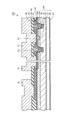
- the MOSFET 101 has a silicon carbide substrate 30, a gate insulating film 41, a gate electrode 50, an interlayer insulating film 42, a source wiring 71 (wiring), an ohmic electrode 61, and a drain electrode 62.
- Silicon carbide substrate 30 has a single crystal wafer 20 of n conductivity type (first conductivity type), a buffer layer 31 of silicon carbide and n conductivity type, and an n conductivity type of silicon carbide Drift layer 32, a pair of p type body regions 33 of p type conductivity (second conductivity type), an n + region 34 of n conductivity type, and ap + region 35 of p conductivity type Have.
- the single crystal wafer 20 has an n-type.
- the buffer layer 31 is epitaxially formed on the main surface of the single crystal wafer 20, and has n-type by being doped with a conductive impurity.
- the drift layer 32 is epitaxially formed on the buffer layer 31 and has n-type by being doped with a conductive type impurity.
- the impurity concentration per volume of the drift layer 32 is lower than the impurity concentration per volume of the buffer layer 31.
- This conductive impurity is, for example, nitrogen (N).
- the pair of p-type body regions 33 are separated from each other on the main surface (upper surface in FIG. 2) of silicon carbide substrate 30.
- the p-type body region 33 has p-type by being doped with a conductive impurity.
- the conductive impurity is, for example, aluminum (Al) or boron (B).
- Each n + region 34 is provided on the main surface of silicon carbide substrate 30 and is separated from drift layer 32 by p type body region 33.
- the impurity concentration of the n + region 34 is higher than the impurity concentration of the drift layer 32.
- P + region 35 extends from above the main surface of silicon carbide substrate 30 to p type body region 33 and is adjacent to n + region 34 on the main surface of silicon carbide substrate 30.
- the impurity concentration of p + region 35 is higher than the impurity concentration of p type body region 33.
- Gate insulating film 41 is provided directly on the main surface of silicon carbide substrate 30 and extends from the upper surface of one n + region 34 to the upper surface of the other n + region 34.
- the gate insulating film is preferably an oxide film, and is made of, for example, silicon dioxide (SiO 2 ).
- the gate electrode 50 is provided directly on the gate insulating film 41 extends over one of the n + region 34 to over the other n + region 34.
- the gate electrode 50 includes a polysilicon film 51 in contact with the gate insulating film 41, a barrier film 52 provided on the polysilicon film 51, and a metal film 53 provided on the barrier film 52.
- the polysilicon film 51 is made of polysilicon to which a conductive impurity is added.
- the thickness of polysilicon film 51 is, for example, about 400 nm.
- the barrier film 52 is made of a material that is not easily silicided as compared to the metal film 53, and for example, titanium (Ti), titanium nitride (TiN), titanium tungsten (TiW), tungsten nitride (WN), or tantalum nitride (TaW) is made from.
- the thickness of barrier film 52 is, for example, about 50 nm.
- the metal film 53 is made of a refractory metal.
- the refractory metal preferably has a melting point above 1000.degree.
- the resistivity of the metal film 53 is lower than the resistivity of the polysilicon film 51.
- the refractory metal is made of any metal of Au, Cu, Si, Ni, Mo, Ta, and W, or an alloy containing at least two of them.
- the thickness of the metal film 53 is, for example, about 50 to 400 nm.
- Interlayer insulating film 42 is provided on silicon carbide substrate 30 provided with gate insulating film 41 and gate electrode 50.
- source contact hole SH substrate contact hole
- gate contact hole GH locally exposing gate electrode 50
- Is provided in interlayer insulating film 42.
- Interlayer insulating film 42 is made of, for example, silicon dioxide (SiO 2 ).
- Source interconnection 71 is electrically connected to silicon carbide substrate 30 via source contact hole SH.
- Source interconnection 71 is electrically insulated from gate electrode 50 by interlayer insulating film 42.
- Source interconnection 71 is made of, for example, aluminum (Al).
- the source wiring 71 has a function as a pad. That is, the source wiring 71 is configured to allow wire bonding thereon.
- Ohmic electrode 61 is interposed between source interconnection 71 and silicon carbide substrate 30.
- the ohmic electrode 61 is made of a material capable of ohmic contact with the n + region 34, specifically made of silicide, for example, made of Ni x Si y (nickel silicide).
- the gate pad 72 is provided on part of the gate electrode 50.
- the gate pad 72 is electrically connected to the gate electrode 50 through the gate contact hole GH.
- Gate pad 72 is made of, for example, aluminum (Al).
- Drain electrode 62 is in contact with single crystal wafer 20 of silicon carbide substrate 30.
- Drain electrode 62 is made of a material capable of making ohmic contact with silicon carbide substrate 30, and specifically made of silicide, for example, made of Ni x Si y (nickel silicide).
- silicon carbide substrate 30 is prepared. Specifically, the following steps are performed.
- a single crystal wafer 20 of silicon carbide is prepared.
- buffer layer 31 and drift layer 32 made of silicon carbide are epitaxially grown sequentially.
- a CVD (Chemical Vapor Deposition) method can be used for this epitaxial growth.
- ion implantation is performed. Specifically, first, ion implantation for forming p-type body region 33 is performed. Specifically, for example, Al (aluminum) ions are implanted into drift layer 32 to form p type body region 33. Next, ion implantation is performed to form n + region 34. Specifically, for example, P (phosphorus) ions are implanted into p type body region 33 to form n + region 34 in p type body region 33. Further, ion implantation is performed to form p + region 35. Specifically, for example, Al ions are implanted into p type body region 33 to form p + region 35 in p type body region 33. The ion implantation can be performed, for example, by forming a mask layer made of silicon dioxide (SiO 2 ) on the main surface of the drift layer 32 and having an opening in a desired region to be subjected to the ion implantation.
- SiO 2 silicon dioxide
- activation heat treatment is performed.
- heat treatment is performed by heating to 1700 ° C. in an inert gas atmosphere such as argon and holding for 30 minutes. This activates the implanted impurities.
- silicon carbide substrate 30 is prepared.
- gate insulating film 41 is formed on silicon carbide substrate 30.
- an oxide film as the gate insulating film 41 is formed by heat treatment of heating to 1300 ° C. and holding for 60 minutes in an oxygen atmosphere. Thereafter, heat treatment using nitrogen monoxide (NO) gas as an atmosphere gas may be performed.
- NO nitrogen monoxide
- As the conditions of this heat treatment for example, conditions of holding at a temperature of 1100 ° C. or more and 1300 ° C. or less for about one hour can be adopted. By such heat treatment, nitrogen atoms are introduced into the interface region between the gate insulating film 41 and the drift layer 32.
- the formation of interface states in the interface region between the gate insulating film 41 and the drift layer 32 can be suppressed, and the channel mobility of the MOSFET 101 finally obtained can be improved.
- the NO gas instead of the NO gas, another gas capable of introducing nitrogen atoms to the interface region between the gate insulating film 41 and the drift layer 32 may be used.
- the heat treatment at a temperature higher than the temperature of this heat treatment may be performed using an argon (Ar) atmosphere in order to further suppress the formation of interface states.
- the gate electrode 50 is formed on the gate insulating film 41.
- the polysilicon film 51 in contact with the gate insulating film 41 is formed.
- Polysilicon film 51 can be formed, for example, by the CVD method.
- barrier film 52 is formed on polysilicon film 51.
- the metal film 53 is formed on the barrier film 52.
- Barrier film 52 and metal film 53 can be formed, for example, by vapor deposition.
- the gate electrode 50 is patterned.
- the patterning can be performed, for example, by photolithography and etching.
- interlayer insulating film 42 is formed on silicon carbide substrate 30 on which gate insulating film 41 and gate electrode 50 are formed.
- Interlayer insulating film 42 can be formed, for example, by the CVD method.
- source contact hole SH partially exposing silicon carbide substrate 30 is formed in interlayer insulating film 42 and gate insulating film 41. This step can be performed, for example, by photolithography and etching.
- a film 61 p is formed on silicon carbide substrate 30 in source contact hole SH.
- Film 61p is made of a material that can be ohmically contacted with silicon carbide substrate 30 by being heated, and specifically made of a material that can be silicided, such as nickel (Ni), for example. It is made from Further, in the present embodiment, on the back surface of single-crystal wafer 20 of silicon carbide substrate 30, a film 62p made of the same material as that of film 61p is formed. This step can be performed, for example, by vapor deposition.
- silicon carbide substrate 30 is heat treated.
- the temperature of the heat treatment is sufficient to promote ohmic contact between silicon carbide substrate 30 and film 61p (FIG. 8), and is preferably over 1000.degree.
- film 61 p formed on the silicon carbide substrate is heated, whereby ohmic electrode 61 is formed from film 61 p.
- drain electrode 62 is formed by heating film 62p (FIG. 8) formed on the back surface of single-crystal wafer 20 of the silicon carbide substrate.
- gate contact hole GH is formed in interlayer insulating film 42. Thereby, a part of the gate electrode 50 is exposed. This step can be performed, for example, by photolithography and etching.
- a film 70 made of metal is formed.
- This metal is, for example, aluminum.
- “metal” is a concept including not only a single metal but also an alloy.
- the film 70 is not limited to a single layer film, and may be a multilayer film.
- the multilayer film can be formed, for example, by forming a barrier film and forming an aluminum film on the barrier film.
- the material of film 70 is the same as the material of each of source interconnection 71 and gate pad 72.
- film 70 is patterned to form source interconnection 71 and gate pad 72 separated from each other, as shown in FIG. Thereby, the MOSFET 101 is obtained.
- gate electrode 50 since gate electrode 50 includes metal film 53 having a resistivity lower than that of polysilicon film 51, as compared to the case where gate electrode 50 is formed only of polysilicon film 51, Electrical resistance can be suppressed. Thus, a current path from the gate pad 72 can be formed by the gate electrode 50 having a small electric resistance.
- the gate electrode is formed only of polysilicon without using metal film 53, the resistivity of polysilicon is higher than that of the metal film, so the resistance is as low as this embodiment. If it is attempted to obtain a gate electrode having the following formula, the thickness of the gate electrode becomes excessively large. Since the gate electrode has a pattern, when the thickness is extremely large, large unevenness corresponding to this pattern will be generated on silicon carbide substrate 30. On the other hand, according to the present embodiment, the thickness of the gate electrode can be reduced by using metal film 53 having a low resistivity, and therefore, the unevenness formed on silicon carbide substrate 30 can be suppressed. .
- heat treatment of silicon carbide substrate 30 forms ohmic electrode 61 between source interconnection 71 and silicon carbide substrate 30.
- the electrical connection between source interconnection 71 and silicon carbide substrate 30 can be made more ohmic.
- the temperature of the heat treatment exceeds 1000 ° C.
- the connection between source interconnection 71 and silicon carbide substrate 30 can be made more ohmic.
- the high melting point metal which is the material of the metal film 53 has a melting point exceeding 1000 ° C.
- heat treatment at more than 1000 ° C. can be performed.
- the source wire 71 and the gate pad 72 are made of the same material.
- the MOSFET 101 can be manufactured more easily than when the material of the source wiring 71 and the material of the gate pad 72 are different. Specifically, by patterning the film 70, the source wiring 71 and the gate pad 72 can be formed simultaneously.
- the main surface of single-crystal wafer 20 facing buffer layer 31 has an off angle of 50 ° or more and 65 ° or less with respect to the ⁇ 0001 ⁇ plane. This can increase channel mobility. Further, it is preferable that an angle between the off direction of the off angle and the ⁇ 01-10> direction be 5 ° or less. Thereby, epitaxial growth on single crystal wafer 20 can be facilitated.
- the main surface preferably has an off angle of -3 ° to 5 ° with respect to the ⁇ 03-38 ⁇ plane in the ⁇ 01-10> direction, and the main surface is substantially the ⁇ 03-38 ⁇ plane. It is more preferable that Thereby, channel mobility can be further improved.
- the angle between the off orientation of the main surface and the ⁇ -2110> direction may be 5 ° or less. Thereby, epitaxial growth on single crystal wafer 20 can be facilitated.
- the main surface be a surface on the carbon surface side of silicon carbide constituting single crystal wafer 20.
- the surface on the carbon surface side is a surface in which m is negative when represented in the surface orientation (hklm). More preferably, this plane is a (0-33-8) plane. Thereby, channel mobility can be further improved.
- the silicon carbide semiconductor device of the present embodiment is a MOSFET 102, more specifically, a VMOSFET (V-groove MOSFET).
- MOSFET 102 has a silicon carbide substrate 30V.
- Silicon carbide substrate 30V has trench TV, and also has p type body region 33V, n type n + region 34V, and relaxation region 36.
- Trench TV has a V-shaped shape, and penetrates n + region 34V and p-type body region 33V to reach drift layer 32.
- the preferred plane orientation of the sidewall of trench TV is the same as the preferred plane orientation of the main surface of single crystal wafer 20 (FIG. 2).
- the relaxation region 36 faces the bottom of the trench TV via the gate insulating film 41.
- the relaxation region 36 has an impurity concentration higher than the impurity concentration of the drift layer 32, and has a function of relaxing the electric field at the bottom of the trench TV.
- buffer layer 31 and drift layer 32 are epitaxially grown sequentially on the main surface of single-crystal wafer 20.
- p-type body region 33V and n + region 34V are formed.
- the p-type body region 33V can be formed by ion implantation or epitaxial growth.
- the n + region 34V can be formed by ion implantation.
- a trench TV is formed.
- the formation of the trench can be performed, for example, by photolithography and etching.
- a relaxation region 36 is formed at the bottom of the trench TV by ion implantation.
- activation heat treatment of impurities is performed.
- substantially the same steps as in FIGS. 4 to 11 of the first embodiment are performed to obtain MOSFET 102 (FIG. 12).
- gate electrode 50 has a portion disposed in trench TV. By the presence of this portion, the electrical resistance of gate electrode 50 is further suppressed by enlarging the cross-sectional area (the area in FIG. 12) of gate electrode 50 without excessively increasing the unevenness on silicon carbide substrate 30. it can.
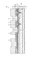
- the silicon carbide semiconductor device of the present embodiment is a MOSFET 103, and has a trench TU instead of the trench TV of the MOSFET 102 (FIG. 12).
- the trench TU has a substantially flat bottom unlike the trench TV.
- the silicon carbide semiconductor device may be a MISFET (Metal Insulator Semiconductor Field Effect Transistor) other than the MOSFET. That is, the gate insulating film 41 is not limited to the oxide.
- the silicon carbide semiconductor device is not limited to the MISFET, and may be another type of device having a gate electrode, and may be, for example, an IGBT (Insulated Gate Bipolar Transistor). Also, the wiring and the gate pad do not necessarily have to be made of the same material.
Abstract
L'invention porte sur une électrode de grille (50) comprenant : une couche de polysilicium (51) en contact avec une couche isolante de grille (41) ; une couche barrière (52) qui est disposée sur la couche de polysilicium (51) ; et une couche métallique (53), qui est disposée sur la couche barrière (52) et qui est composée d'un métal de point de fusion élevé. Une couche isolante intercouche (42) est disposée pour recouvrir la couche isolante de grille (41) et l'électrode de grille (50) qui est disposée sur la couche isolante de grille (41). En outre, la couche isolante intercouche (42) comprend une fenêtre de contact au substrat (SH), à partir de laquelle un substrat en carbure de silicium (30) est en partie exposé dans une zone en contact avec la couche isolante de grille (41). Un câblage (71) est électriquement connecté au substrat en carbure de silicium (30) par l'intermédiaire de la fenêtre de contact au substrat (SH) et il est électriquement isolé de l'électrode de grille (50) au moyen de la couche isolante intercouche (42).
Priority Applications (3)
| Application Number | Priority Date | Filing Date | Title |
|---|---|---|---|
| KR1020137027717A KR20140021609A (ko) | 2011-06-15 | 2012-05-29 | 탄화규소 반도체 장치 및 그 제조 방법 |
| EP12800187.2A EP2722892A4 (fr) | 2011-06-15 | 2012-05-29 | Dispositif à semi-conducteur en carbure de silicium et son procédé de fabrication |
| CN201280023455.4A CN103548144A (zh) | 2011-06-15 | 2012-05-29 | 碳化硅半导体器件及其制造方法 |
Applications Claiming Priority (2)
| Application Number | Priority Date | Filing Date | Title |
|---|---|---|---|
| JP2011-132784 | 2011-06-15 | ||
| JP2011132784A JP2013004636A (ja) | 2011-06-15 | 2011-06-15 | 炭化珪素半導体装置およびその製造方法 |
Publications (1)
| Publication Number | Publication Date |
|---|---|
| WO2012172965A1 true WO2012172965A1 (fr) | 2012-12-20 |
Family
ID=47352981
Family Applications (1)
| Application Number | Title | Priority Date | Filing Date |
|---|---|---|---|
| PCT/JP2012/063722 WO2012172965A1 (fr) | 2011-06-15 | 2012-05-29 | Dispositif à semi-conducteur en carbure de silicium et son procédé de fabrication |
Country Status (7)
| Country | Link |
|---|---|
| US (1) | US20120319134A1 (fr) |
| EP (1) | EP2722892A4 (fr) |
| JP (1) | JP2013004636A (fr) |
| KR (1) | KR20140021609A (fr) |
| CN (1) | CN103548144A (fr) |
| TW (1) | TW201308621A (fr) |
| WO (1) | WO2012172965A1 (fr) |
Cited By (1)
| Publication number | Priority date | Publication date | Assignee | Title |
|---|---|---|---|---|
| JP2019046975A (ja) * | 2017-09-01 | 2019-03-22 | トヨタ自動車株式会社 | スイッチング装置 |
Families Citing this family (12)
| Publication number | Priority date | Publication date | Assignee | Title |
|---|---|---|---|---|
| JP2015015352A (ja) * | 2013-07-04 | 2015-01-22 | 住友電気工業株式会社 | 炭化珪素半導体装置の製造方法 |
| JP6098417B2 (ja) | 2013-07-26 | 2017-03-22 | 住友電気工業株式会社 | 炭化珪素半導体装置およびその製造方法 |
| JP2015156429A (ja) * | 2014-02-20 | 2015-08-27 | 住友電気工業株式会社 | 炭化珪素半導体装置およびその製造方法 |
| JP6295797B2 (ja) * | 2014-04-10 | 2018-03-20 | 住友電気工業株式会社 | 炭化珪素半導体装置およびその製造方法 |
| CN106463541B (zh) * | 2014-05-23 | 2019-05-21 | 松下知识产权经营株式会社 | 碳化硅半导体装置 |
| JP2017028219A (ja) * | 2015-07-28 | 2017-02-02 | 三菱電機株式会社 | 炭化珪素半導体装置およびその製造方法 |
| JP2018074088A (ja) * | 2016-11-02 | 2018-05-10 | 富士電機株式会社 | 半導体装置 |
| DE102019109368A1 (de) | 2018-05-15 | 2019-11-21 | Infineon Technologies Ag | Halbleitervorrichtung mit siliziumcarbidkörper und herstellungsverfahren |
| JP7180425B2 (ja) * | 2019-02-06 | 2022-11-30 | 住友電気工業株式会社 | 炭化珪素半導体装置 |
| US20210343847A1 (en) * | 2020-04-30 | 2021-11-04 | Cree, Inc. | Diffusion and/or enhancement layers for electrical contact regions |
| IT202100003653A1 (it) * | 2021-02-17 | 2022-08-17 | St Microelectronics Srl | Dispositivo mosfet di carburo di silicio, a conduzione verticale, avente struttura di polarizzazione di porta perfezionata e relativo procedimento di fabbricazione |
| US20230335595A1 (en) * | 2022-04-13 | 2023-10-19 | Leap Semiconductor Corp. | Silicon carbide semiconductor power transistor and method of manufacturing the same |
Citations (4)
| Publication number | Priority date | Publication date | Assignee | Title |
|---|---|---|---|---|
| JPH07273326A (ja) * | 1994-03-31 | 1995-10-20 | Toshiba Corp | 半導体装置とその製造方法 |
| JP2001284587A (ja) * | 2000-03-28 | 2001-10-12 | Kaga Toshiba Electron Kk | 半導体装置およびその製造方法 |
| JP2010171417A (ja) | 2008-12-25 | 2010-08-05 | Rohm Co Ltd | 半導体装置 |
| WO2010125661A1 (fr) * | 2009-04-30 | 2010-11-04 | 三菱電機株式会社 | Dispositif de semi-conducteur et son procédé de fabrication |
Family Cites Families (13)
| Publication number | Priority date | Publication date | Assignee | Title |
|---|---|---|---|---|
| US5736753A (en) * | 1994-09-12 | 1998-04-07 | Hitachi, Ltd. | Semiconductor device for improved power conversion having a hexagonal-system single-crystal silicon carbide |
| US6133587A (en) * | 1996-01-23 | 2000-10-17 | Denso Corporation | Silicon carbide semiconductor device and process for manufacturing same |
| JP3471509B2 (ja) * | 1996-01-23 | 2003-12-02 | 株式会社デンソー | 炭化珪素半導体装置 |
| JPH11251592A (ja) * | 1998-01-05 | 1999-09-07 | Denso Corp | 炭化珪素半導体装置 |
| US6274905B1 (en) * | 1999-06-30 | 2001-08-14 | Fairchild Semiconductor Corporation | Trench structure substantially filled with high-conductivity material |
| JP4917246B2 (ja) * | 2003-11-17 | 2012-04-18 | ローム株式会社 | 半導体装置およびその製造方法 |
| JP4830285B2 (ja) * | 2004-11-08 | 2011-12-07 | 株式会社デンソー | 炭化珪素半導体装置の製造方法 |
| GB2424312B (en) * | 2005-03-14 | 2010-03-03 | Denso Corp | Method of forming an ohmic contact in wide band semiconductor |
| JP5017823B2 (ja) * | 2005-09-12 | 2012-09-05 | 富士電機株式会社 | 半導体素子の製造方法 |
| JP4046140B1 (ja) * | 2006-11-29 | 2008-02-13 | 住友電気工業株式会社 | 炭化珪素半導体装置の製造方法 |
| JP4450241B2 (ja) * | 2007-03-20 | 2010-04-14 | 株式会社デンソー | 炭化珪素半導体装置の製造方法 |
| CN102017159B (zh) * | 2008-09-12 | 2013-06-12 | 住友电气工业株式会社 | 碳化硅半导体器件及其制造方法 |
| JP5721351B2 (ja) * | 2009-07-21 | 2015-05-20 | ローム株式会社 | 半導体装置 |
-
2011
- 2011-06-15 JP JP2011132784A patent/JP2013004636A/ja active Pending
-
2012
- 2012-05-29 WO PCT/JP2012/063722 patent/WO2012172965A1/fr active Application Filing
- 2012-05-29 EP EP12800187.2A patent/EP2722892A4/fr not_active Withdrawn
- 2012-05-29 KR KR1020137027717A patent/KR20140021609A/ko not_active Application Discontinuation
- 2012-05-29 CN CN201280023455.4A patent/CN103548144A/zh active Pending
- 2012-06-07 TW TW101120545A patent/TW201308621A/zh unknown
- 2012-06-14 US US13/523,600 patent/US20120319134A1/en not_active Abandoned
Patent Citations (4)
| Publication number | Priority date | Publication date | Assignee | Title |
|---|---|---|---|---|
| JPH07273326A (ja) * | 1994-03-31 | 1995-10-20 | Toshiba Corp | 半導体装置とその製造方法 |
| JP2001284587A (ja) * | 2000-03-28 | 2001-10-12 | Kaga Toshiba Electron Kk | 半導体装置およびその製造方法 |
| JP2010171417A (ja) | 2008-12-25 | 2010-08-05 | Rohm Co Ltd | 半導体装置 |
| WO2010125661A1 (fr) * | 2009-04-30 | 2010-11-04 | 三菱電機株式会社 | Dispositif de semi-conducteur et son procédé de fabrication |
Non-Patent Citations (1)
| Title |
|---|
| See also references of EP2722892A4 * |
Cited By (1)
| Publication number | Priority date | Publication date | Assignee | Title |
|---|---|---|---|---|
| JP2019046975A (ja) * | 2017-09-01 | 2019-03-22 | トヨタ自動車株式会社 | スイッチング装置 |
Also Published As
| Publication number | Publication date |
|---|---|
| KR20140021609A (ko) | 2014-02-20 |
| EP2722892A4 (fr) | 2015-01-21 |
| TW201308621A (zh) | 2013-02-16 |
| EP2722892A1 (fr) | 2014-04-23 |
| US20120319134A1 (en) | 2012-12-20 |
| CN103548144A (zh) | 2014-01-29 |
| JP2013004636A (ja) | 2013-01-07 |
Similar Documents
| Publication | Publication Date | Title |
|---|---|---|
| WO2012172965A1 (fr) | Dispositif à semi-conducteur en carbure de silicium et son procédé de fabrication | |
| US7829416B2 (en) | Silicon carbide semiconductor device and method for producing the same | |
| US20150287598A1 (en) | Semiconductor device and method for manufacturing same | |
| TWI532172B (zh) | Semiconductor device and manufacturing method thereof | |
| US8846531B2 (en) | Method of manufacturing an ohmic electrode containing titanium, aluminum and silicon on a silicon carbide surface | |
| JP5994604B2 (ja) | 炭化珪素半導体装置およびその製造方法 | |
| JP5728954B2 (ja) | 炭化珪素半導体装置の製造方法 | |
| JP5745974B2 (ja) | 半導体装置およびその製造方法 | |
| WO2012165008A1 (fr) | Dispositif à semi-conducteur en carbure de silicium, et procédé de fabrication associé | |
| US9601581B2 (en) | Semiconductor device and method for producing the same | |
| JP2012243966A (ja) | 半導体装置 | |
| WO2014046073A1 (fr) | Dispositif à semi-conducteur de carbure de silicium et son procédé de fabrication | |
| JP6295797B2 (ja) | 炭化珪素半導体装置およびその製造方法 | |
| US20160056040A1 (en) | Method for manufacturing silicon carbide semiconductor device | |
| JP5704003B2 (ja) | 半導体装置の製造方法 | |
| JP2014127660A (ja) | 炭化珪素ダイオード、炭化珪素トランジスタおよび炭化珪素半導体装置の製造方法 | |
| JP7156313B2 (ja) | 炭化珪素半導体装置 | |
| WO2023058377A1 (fr) | Dispositif à semi-conducteur au carbure de silicium | |
| WO2019198167A1 (fr) | Procédé de fabrication de dispositif à semi-conducteur et dispositif à semi-conducteur | |
| JP2022187367A (ja) | 炭化珪素半導体装置の製造方法および炭化珪素半導体装置 | |
| JP5439856B2 (ja) | 絶縁ゲート型電界効果トランジスタ | |
| JP2022146601A (ja) | 炭化珪素半導体装置及び炭化珪素半導体装置の製造方法 |
Legal Events
| Date | Code | Title | Description |
|---|---|---|---|
| 121 | Ep: the epo has been informed by wipo that ep was designated in this application |
Ref document number: 12800187 Country of ref document: EP Kind code of ref document: A1 |
|
| WWE | Wipo information: entry into national phase |
Ref document number: 2012800187 Country of ref document: EP |
|
| ENP | Entry into the national phase |
Ref document number: 20137027717 Country of ref document: KR Kind code of ref document: A |
|
| NENP | Non-entry into the national phase |
Ref country code: DE |