WO2012172965A1 - Silicon carbide semiconductor device and method for manufacturing same - Google Patents
Silicon carbide semiconductor device and method for manufacturing same Download PDFInfo
- Publication number
- WO2012172965A1 WO2012172965A1 PCT/JP2012/063722 JP2012063722W WO2012172965A1 WO 2012172965 A1 WO2012172965 A1 WO 2012172965A1 JP 2012063722 W JP2012063722 W JP 2012063722W WO 2012172965 A1 WO2012172965 A1 WO 2012172965A1
- Authority
- WO
- WIPO (PCT)
- Prior art keywords
- silicon carbide
- insulating film
- film
- gate
- gate electrode
- Prior art date
Links
- HBMJWWWQQXIZIP-UHFFFAOYSA-N silicon carbide Chemical compound [Si+]#[C-] HBMJWWWQQXIZIP-UHFFFAOYSA-N 0.000 title claims abstract description 114
- 229910010271 silicon carbide Inorganic materials 0.000 title claims abstract description 114
- 239000004065 semiconductor Substances 0.000 title claims description 45
- 238000004519 manufacturing process Methods 0.000 title claims description 24
- 238000000034 method Methods 0.000 title claims description 19
- 239000000758 substrate Substances 0.000 claims abstract description 80
- 229910052751 metal Inorganic materials 0.000 claims abstract description 31
- 239000002184 metal Substances 0.000 claims abstract description 31
- 229910021420 polycrystalline silicon Inorganic materials 0.000 claims abstract description 29
- 229920005591 polysilicon Polymers 0.000 claims abstract description 29
- 239000011229 interlayer Substances 0.000 claims abstract description 25
- 230000004888 barrier function Effects 0.000 claims abstract description 20
- 230000008018 melting Effects 0.000 claims abstract description 9
- 238000002844 melting Methods 0.000 claims abstract description 9
- 238000010438 heat treatment Methods 0.000 claims description 21
- 239000000463 material Substances 0.000 claims description 17
- 239000003870 refractory metal Substances 0.000 claims description 9
- 238000000059 patterning Methods 0.000 claims description 5
- 239000004020 conductor Substances 0.000 claims description 4
- 239000010410 layer Substances 0.000 description 24
- 210000000746 body region Anatomy 0.000 description 17
- 239000012535 impurity Substances 0.000 description 16
- 239000013078 crystal Substances 0.000 description 15
- 238000005468 ion implantation Methods 0.000 description 9
- MWUXSHHQAYIFBG-UHFFFAOYSA-N Nitric oxide Chemical compound O=[N] MWUXSHHQAYIFBG-UHFFFAOYSA-N 0.000 description 6
- VYPSYNLAJGMNEJ-UHFFFAOYSA-N Silicium dioxide Chemical compound O=[Si]=O VYPSYNLAJGMNEJ-UHFFFAOYSA-N 0.000 description 6
- 229910052782 aluminium Inorganic materials 0.000 description 6
- XAGFODPZIPBFFR-UHFFFAOYSA-N aluminium Chemical compound [Al] XAGFODPZIPBFFR-UHFFFAOYSA-N 0.000 description 6
- PXHVJJICTQNCMI-UHFFFAOYSA-N nickel Substances [Ni] PXHVJJICTQNCMI-UHFFFAOYSA-N 0.000 description 6
- XKRFYHLGVUSROY-UHFFFAOYSA-N Argon Chemical compound [Ar] XKRFYHLGVUSROY-UHFFFAOYSA-N 0.000 description 4
- 238000005229 chemical vapour deposition Methods 0.000 description 4
- 238000005530 etching Methods 0.000 description 4
- 239000007789 gas Substances 0.000 description 4
- 238000000206 photolithography Methods 0.000 description 4
- 229910004298 SiO 2 Inorganic materials 0.000 description 3
- 230000015572 biosynthetic process Effects 0.000 description 3
- 150000002500 ions Chemical class 0.000 description 3
- 125000004433 nitrogen atom Chemical group N* 0.000 description 3
- 235000012239 silicon dioxide Nutrition 0.000 description 3
- 239000000377 silicon dioxide Substances 0.000 description 3
- IJGRMHOSHXDMSA-UHFFFAOYSA-N Atomic nitrogen Chemical compound N#N IJGRMHOSHXDMSA-UHFFFAOYSA-N 0.000 description 2
- OKTJSMMVPCPJKN-UHFFFAOYSA-N Carbon Chemical compound [C] OKTJSMMVPCPJKN-UHFFFAOYSA-N 0.000 description 2
- 230000004913 activation Effects 0.000 description 2
- 229910045601 alloy Inorganic materials 0.000 description 2
- 239000000956 alloy Substances 0.000 description 2
- 229910052786 argon Inorganic materials 0.000 description 2
- 229910052799 carbon Inorganic materials 0.000 description 2
- 230000005669 field effect Effects 0.000 description 2
- 230000004048 modification Effects 0.000 description 2
- 238000012986 modification Methods 0.000 description 2
- 229910052759 nickel Inorganic materials 0.000 description 2
- 229910021334 nickel silicide Inorganic materials 0.000 description 2
- RUFLMLWJRZAWLJ-UHFFFAOYSA-N nickel silicide Chemical compound [Ni]=[Si]=[Ni] RUFLMLWJRZAWLJ-UHFFFAOYSA-N 0.000 description 2
- 229910021332 silicide Inorganic materials 0.000 description 2
- FVBUAEGBCNSCDD-UHFFFAOYSA-N silicide(4-) Chemical compound [Si-4] FVBUAEGBCNSCDD-UHFFFAOYSA-N 0.000 description 2
- 239000010936 titanium Substances 0.000 description 2
- 238000007740 vapor deposition Methods 0.000 description 2
- ZOXJGFHDIHLPTG-UHFFFAOYSA-N Boron Chemical compound [B] ZOXJGFHDIHLPTG-UHFFFAOYSA-N 0.000 description 1
- OAICVXFJPJFONN-UHFFFAOYSA-N Phosphorus Chemical compound [P] OAICVXFJPJFONN-UHFFFAOYSA-N 0.000 description 1
- RTAQQCXQSZGOHL-UHFFFAOYSA-N Titanium Chemical compound [Ti] RTAQQCXQSZGOHL-UHFFFAOYSA-N 0.000 description 1
- NRTOMJZYCJJWKI-UHFFFAOYSA-N Titanium nitride Chemical compound [Ti]#N NRTOMJZYCJJWKI-UHFFFAOYSA-N 0.000 description 1
- QVGXLLKOCUKJST-UHFFFAOYSA-N atomic oxygen Chemical compound [O] QVGXLLKOCUKJST-UHFFFAOYSA-N 0.000 description 1
- IVHJCRXBQPGLOV-UHFFFAOYSA-N azanylidynetungsten Chemical compound [W]#N IVHJCRXBQPGLOV-UHFFFAOYSA-N 0.000 description 1
- 229910052796 boron Inorganic materials 0.000 description 1
- 229910052802 copper Inorganic materials 0.000 description 1
- 230000005684 electric field Effects 0.000 description 1
- 229910052737 gold Inorganic materials 0.000 description 1
- 239000011261 inert gas Substances 0.000 description 1
- 239000012212 insulator Substances 0.000 description 1
- 229910044991 metal oxide Inorganic materials 0.000 description 1
- 150000004706 metal oxides Chemical class 0.000 description 1
- 229910052750 molybdenum Inorganic materials 0.000 description 1
- 229910052757 nitrogen Inorganic materials 0.000 description 1
- 239000001301 oxygen Substances 0.000 description 1
- 229910052760 oxygen Inorganic materials 0.000 description 1
- 229910052698 phosphorus Inorganic materials 0.000 description 1
- 239000011574 phosphorus Substances 0.000 description 1
- 230000002040 relaxant effect Effects 0.000 description 1
- 229910052710 silicon Inorganic materials 0.000 description 1
- 239000002356 single layer Substances 0.000 description 1
- 229910052715 tantalum Inorganic materials 0.000 description 1
- MZLGASXMSKOWSE-UHFFFAOYSA-N tantalum nitride Chemical compound [Ta]#N MZLGASXMSKOWSE-UHFFFAOYSA-N 0.000 description 1
- 229910052719 titanium Inorganic materials 0.000 description 1
- MAKDTFFYCIMFQP-UHFFFAOYSA-N titanium tungsten Chemical compound [Ti].[W] MAKDTFFYCIMFQP-UHFFFAOYSA-N 0.000 description 1
- 229910052721 tungsten Inorganic materials 0.000 description 1
Images


Classifications
-
- H—ELECTRICITY
- H01—ELECTRIC ELEMENTS
- H01L—SEMICONDUCTOR DEVICES NOT COVERED BY CLASS H10
- H01L29/00—Semiconductor devices adapted for rectifying, amplifying, oscillating or switching, or capacitors or resistors with at least one potential-jump barrier or surface barrier, e.g. PN junction depletion layer or carrier concentration layer; Details of semiconductor bodies or of electrodes thereof ; Multistep manufacturing processes therefor
- H01L29/66—Types of semiconductor device ; Multistep manufacturing processes therefor
- H01L29/68—Types of semiconductor device ; Multistep manufacturing processes therefor controllable by only the electric current supplied, or only the electric potential applied, to an electrode which does not carry the current to be rectified, amplified or switched
- H01L29/76—Unipolar devices, e.g. field effect transistors
- H01L29/772—Field effect transistors
- H01L29/78—Field effect transistors with field effect produced by an insulated gate
- H01L29/7801—DMOS transistors, i.e. MISFETs with a channel accommodating body or base region adjoining a drain drift region
- H01L29/7802—Vertical DMOS transistors, i.e. VDMOS transistors
-
- H—ELECTRICITY
- H01—ELECTRIC ELEMENTS
- H01L—SEMICONDUCTOR DEVICES NOT COVERED BY CLASS H10
- H01L29/00—Semiconductor devices adapted for rectifying, amplifying, oscillating or switching, or capacitors or resistors with at least one potential-jump barrier or surface barrier, e.g. PN junction depletion layer or carrier concentration layer; Details of semiconductor bodies or of electrodes thereof ; Multistep manufacturing processes therefor
- H01L29/02—Semiconductor bodies ; Multistep manufacturing processes therefor
- H01L29/12—Semiconductor bodies ; Multistep manufacturing processes therefor characterised by the materials of which they are formed
- H01L29/16—Semiconductor bodies ; Multistep manufacturing processes therefor characterised by the materials of which they are formed including, apart from doping materials or other impurities, only elements of Group IV of the Periodic System
- H01L29/1608—Silicon carbide
-
- H—ELECTRICITY
- H01—ELECTRIC ELEMENTS
- H01L—SEMICONDUCTOR DEVICES NOT COVERED BY CLASS H10
- H01L29/00—Semiconductor devices adapted for rectifying, amplifying, oscillating or switching, or capacitors or resistors with at least one potential-jump barrier or surface barrier, e.g. PN junction depletion layer or carrier concentration layer; Details of semiconductor bodies or of electrodes thereof ; Multistep manufacturing processes therefor
- H01L29/40—Electrodes ; Multistep manufacturing processes therefor
- H01L29/43—Electrodes ; Multistep manufacturing processes therefor characterised by the materials of which they are formed
- H01L29/49—Metal-insulator-semiconductor electrodes, e.g. gates of MOSFET
- H01L29/4916—Metal-insulator-semiconductor electrodes, e.g. gates of MOSFET the conductor material next to the insulator being a silicon layer, e.g. polysilicon doped with boron, phosphorus or nitrogen
- H01L29/4925—Metal-insulator-semiconductor electrodes, e.g. gates of MOSFET the conductor material next to the insulator being a silicon layer, e.g. polysilicon doped with boron, phosphorus or nitrogen with a multiple layer structure, e.g. several silicon layers with different crystal structure or grain arrangement
- H01L29/4941—Metal-insulator-semiconductor electrodes, e.g. gates of MOSFET the conductor material next to the insulator being a silicon layer, e.g. polysilicon doped with boron, phosphorus or nitrogen with a multiple layer structure, e.g. several silicon layers with different crystal structure or grain arrangement with a barrier layer between the silicon and the metal or metal silicide upper layer, e.g. Silicide/TiN/Polysilicon
-
- H—ELECTRICITY
- H01—ELECTRIC ELEMENTS
- H01L—SEMICONDUCTOR DEVICES NOT COVERED BY CLASS H10
- H01L29/00—Semiconductor devices adapted for rectifying, amplifying, oscillating or switching, or capacitors or resistors with at least one potential-jump barrier or surface barrier, e.g. PN junction depletion layer or carrier concentration layer; Details of semiconductor bodies or of electrodes thereof ; Multistep manufacturing processes therefor
- H01L29/66—Types of semiconductor device ; Multistep manufacturing processes therefor
- H01L29/66007—Multistep manufacturing processes
- H01L29/66075—Multistep manufacturing processes of devices having semiconductor bodies comprising group 14 or group 13/15 materials
- H01L29/66227—Multistep manufacturing processes of devices having semiconductor bodies comprising group 14 or group 13/15 materials the devices being controllable only by the electric current supplied or the electric potential applied, to an electrode which does not carry the current to be rectified, amplified or switched, e.g. three-terminal devices
- H01L29/66409—Unipolar field-effect transistors
- H01L29/66477—Unipolar field-effect transistors with an insulated gate, i.e. MISFET
- H01L29/66674—DMOS transistors, i.e. MISFETs with a channel accommodating body or base region adjoining a drain drift region
- H01L29/66712—Vertical DMOS transistors, i.e. VDMOS transistors
-
- H—ELECTRICITY
- H01—ELECTRIC ELEMENTS
- H01L—SEMICONDUCTOR DEVICES NOT COVERED BY CLASS H10
- H01L29/00—Semiconductor devices adapted for rectifying, amplifying, oscillating or switching, or capacitors or resistors with at least one potential-jump barrier or surface barrier, e.g. PN junction depletion layer or carrier concentration layer; Details of semiconductor bodies or of electrodes thereof ; Multistep manufacturing processes therefor
- H01L29/66—Types of semiconductor device ; Multistep manufacturing processes therefor
- H01L29/68—Types of semiconductor device ; Multistep manufacturing processes therefor controllable by only the electric current supplied, or only the electric potential applied, to an electrode which does not carry the current to be rectified, amplified or switched
- H01L29/76—Unipolar devices, e.g. field effect transistors
- H01L29/772—Field effect transistors
- H01L29/78—Field effect transistors with field effect produced by an insulated gate
- H01L29/7801—DMOS transistors, i.e. MISFETs with a channel accommodating body or base region adjoining a drain drift region
- H01L29/7802—Vertical DMOS transistors, i.e. VDMOS transistors
- H01L29/7811—Vertical DMOS transistors, i.e. VDMOS transistors with an edge termination structure
-
- H—ELECTRICITY
- H01—ELECTRIC ELEMENTS
- H01L—SEMICONDUCTOR DEVICES NOT COVERED BY CLASS H10
- H01L29/00—Semiconductor devices adapted for rectifying, amplifying, oscillating or switching, or capacitors or resistors with at least one potential-jump barrier or surface barrier, e.g. PN junction depletion layer or carrier concentration layer; Details of semiconductor bodies or of electrodes thereof ; Multistep manufacturing processes therefor
- H01L29/66—Types of semiconductor device ; Multistep manufacturing processes therefor
- H01L29/68—Types of semiconductor device ; Multistep manufacturing processes therefor controllable by only the electric current supplied, or only the electric potential applied, to an electrode which does not carry the current to be rectified, amplified or switched
- H01L29/76—Unipolar devices, e.g. field effect transistors
- H01L29/772—Field effect transistors
- H01L29/78—Field effect transistors with field effect produced by an insulated gate
- H01L29/7801—DMOS transistors, i.e. MISFETs with a channel accommodating body or base region adjoining a drain drift region
- H01L29/7802—Vertical DMOS transistors, i.e. VDMOS transistors
- H01L29/7813—Vertical DMOS transistors, i.e. VDMOS transistors with trench gate electrode, e.g. UMOS transistors
-
- H—ELECTRICITY
- H01—ELECTRIC ELEMENTS
- H01L—SEMICONDUCTOR DEVICES NOT COVERED BY CLASS H10
- H01L29/00—Semiconductor devices adapted for rectifying, amplifying, oscillating or switching, or capacitors or resistors with at least one potential-jump barrier or surface barrier, e.g. PN junction depletion layer or carrier concentration layer; Details of semiconductor bodies or of electrodes thereof ; Multistep manufacturing processes therefor
- H01L29/02—Semiconductor bodies ; Multistep manufacturing processes therefor
- H01L29/06—Semiconductor bodies ; Multistep manufacturing processes therefor characterised by their shape; characterised by the shapes, relative sizes, or dispositions of the semiconductor regions ; characterised by the concentration or distribution of impurities within semiconductor regions
- H01L29/08—Semiconductor bodies ; Multistep manufacturing processes therefor characterised by their shape; characterised by the shapes, relative sizes, or dispositions of the semiconductor regions ; characterised by the concentration or distribution of impurities within semiconductor regions with semiconductor regions connected to an electrode carrying current to be rectified, amplified or switched and such electrode being part of a semiconductor device which comprises three or more electrodes
- H01L29/0843—Source or drain regions of field-effect devices
- H01L29/0847—Source or drain regions of field-effect devices of field-effect transistors with insulated gate
- H01L29/0852—Source or drain regions of field-effect devices of field-effect transistors with insulated gate of DMOS transistors
- H01L29/0873—Drain regions
- H01L29/0878—Impurity concentration or distribution
-
- H—ELECTRICITY
- H01—ELECTRIC ELEMENTS
- H01L—SEMICONDUCTOR DEVICES NOT COVERED BY CLASS H10
- H01L29/00—Semiconductor devices adapted for rectifying, amplifying, oscillating or switching, or capacitors or resistors with at least one potential-jump barrier or surface barrier, e.g. PN junction depletion layer or carrier concentration layer; Details of semiconductor bodies or of electrodes thereof ; Multistep manufacturing processes therefor
- H01L29/40—Electrodes ; Multistep manufacturing processes therefor
- H01L29/43—Electrodes ; Multistep manufacturing processes therefor characterised by the materials of which they are formed
- H01L29/45—Ohmic electrodes
Definitions
- the present invention relates to a silicon carbide semiconductor device and a method of manufacturing the same, and more particularly to a silicon carbide semiconductor device having a gate electrode and a method of manufacturing the same.
- Patent Document 1 JP-A-2010-171417 discloses a MOSFET (Metal Oxide Semiconductor Field Effect Transistor) having a silicon carbide substrate, a gate pad, and a gate electrode.
- the gate electrode is made of polysilicon.
- the present invention has been made to address such a problem, and it is an object of the present invention to provide a silicon carbide semiconductor device capable of suppressing the electrical resistance of a gate electrode and a method of manufacturing the same.
- the silicon carbide semiconductor device of the present invention has a silicon carbide substrate, a gate insulating film, a gate electrode, an interlayer insulating film, and a wiring.
- the gate insulating film is provided on a silicon carbide substrate.
- the gate electrode is provided on the gate insulating film.
- the gate electrode includes a polysilicon film in contact with the gate insulating film, a barrier film provided on the polysilicon film, and a metal film provided on the barrier film and made of a high melting point metal.
- the interlayer insulating film is arranged to cover the gate insulating film and the gate electrode provided on the gate insulating film.
- the interlayer insulating film has a substrate contact hole that partially exposes the silicon carbide substrate in a region in contact with the gate insulating film.
- the wiring is electrically connected to the silicon carbide substrate through the substrate contact hole, and is electrically isolated from the gate electrode by the interlayer insulating film.
- the gate electrode since the gate electrode includes the refractory metal film having a lower resistivity than the polysilicon film, compared to the case where the gate electrode is formed of only the polysilicon film, The electrical resistance of the gate electrode can be suppressed.
- the interlayer insulating film has a gate contact hole partially exposing the gate electrode.
- the silicon carbide semiconductor device has a gate pad electrically connected to the gate electrode through the gate contact hole.
- a current path from the gate pad can be formed by the gate electrode having a small electric resistance.
- the wiring and the gate pad are made of the same material. Thereby, the silicon carbide semiconductor device can be manufactured more easily than when the material of the wiring and the material of the gate pad are different.
- the refractory metal has a melting point above 1000 ° C.
- the heat treatment can be performed at a temperature higher than 1000.degree.
- the silicon carbide substrate may be provided with a trench, and at least a part of the gate electrode may be disposed in the trench. Thereby, the electrical resistance of the gate electrode can be further suppressed.
- the method for manufacturing a silicon carbide semiconductor device of the present invention has the following steps.
- a gate insulating film is formed on the silicon carbide substrate.
- a gate electrode is formed on the gate insulating film.
- the step of forming the gate electrode the step of forming a polysilicon film in contact with the gate insulating film, the step of forming a barrier film on the polysilicon film, and the step of forming a metal film made of refractory metal on the barrier film
- the step of An interlayer insulating film is formed to cover the gate insulating film and the gate electrode provided on the gate insulating film, and has a substrate contact hole that partially exposes the silicon carbide substrate in a region in contact with the gate insulating film.
- An interconnection electrically connected to the silicon carbide substrate through the substrate contact hole and electrically insulated from the gate electrode by the interlayer insulating film is formed.
- the gate electrode since the gate electrode includes a refractory metal film having a resistivity lower than that of the polysilicon film, the gate electrode is formed of only the polysilicon film. Thus, the electrical resistance of the gate electrode can be suppressed.
- the silicon carbide substrate is heat-treated to make the electrical connection between the wiring and the silicon carbide substrate more ohmic.
- the electrical connection between the wiring and the silicon carbide substrate can be made more ohmic.
- the step of heat-treating the silicon carbide substrate includes the step of heating the silicon carbide substrate to a temperature exceeding 1000 ° C. Thereby, the electrical connection between the wiring and the silicon carbide substrate can be made more ohmic.
- the step of forming the wiring includes the steps of forming a conductor film in contact with each of the gate electrode and the silicon carbide substrate, and patterning the conductor film.
- the patterning process By the patterning process, a wire and a gate pad provided on part of the gate electrode are formed.
- the silicon carbide semiconductor device can be manufactured more easily than when the wiring and the gate pad are separately formed.
- a trench may be formed in the silicon carbide substrate, and at least a portion of the gate electrode may be disposed in the trench. Thereby, the electrical resistance of the gate electrode can be further suppressed.
- the electrical resistance can be suppressed.
- FIG. 1 is a plan view schematically showing a structure of a silicon carbide semiconductor device in a first embodiment.
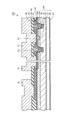
- FIG. 2 is a schematic cross-sectional view taken along line II-II of FIG.
- FIG. 3 is a cross sectional view schematically showing a first step of a method of manufacturing the silicon carbide semiconductor device of FIG. 1 in a view corresponding to the view of FIG. 2.
- FIG. 3 is a cross sectional view schematically showing a second step of the method for manufacturing the silicon carbide semiconductor device of FIG. 1 in a view corresponding to the view of FIG. 2.
- FIG. 13 is a cross sectional view schematically showing a third step of the method for manufacturing the silicon carbide semiconductor device of FIG. 1 in a view corresponding to the view of FIG. 2.
- FIG. 1 is a plan view schematically showing a structure of a silicon carbide semiconductor device in a first embodiment.
- FIG. 2 is a schematic cross-sectional view taken along line II-II of FIG.
- FIG. 3 is
- FIG. 14 is a cross sectional view schematically showing a fourth step of the method for manufacturing the silicon carbide semiconductor device of FIG. 1 in a view corresponding to the view of FIG. 2.
- FIG. 13 is a cross sectional view schematically showing a fifth step of the method for manufacturing the silicon carbide semiconductor device of FIG. 1 in a view corresponding to the view of FIG. 2.
- FIG. 13 is a cross sectional view schematically showing a sixth step of the method for manufacturing the silicon carbide semiconductor device of FIG. 1 in a view corresponding to the view of FIG. 2.
- FIG. 13 is a cross sectional view schematically showing a seventh step of the method for manufacturing the silicon carbide semiconductor device of FIG. 1 in a view corresponding to the view of FIG. 2.
- FIG. 13 is a cross sectional view schematically showing a eighth step of the method for manufacturing the silicon carbide semiconductor device of FIG. 1 in a view corresponding to the view of FIG. 2.
- FIG. 13 is a cross sectional view schematically showing a ninth step of the method for manufacturing the silicon carbide semiconductor device of FIG. 1 in a view corresponding to the view of FIG. 2.
- FIG. 3 is a cross sectional view schematically showing a structure of a silicon carbide semiconductor device in a second embodiment in a view corresponding to the view in FIG. 2.
- FIG. 13 is a cross sectional view schematically showing a first step of a method of manufacturing the silicon carbide semiconductor device of FIG. 12 in a view corresponding to the view of FIG. 12.
- FIG. 13 is a cross sectional view schematically showing a second step of the method for manufacturing the silicon carbide semiconductor device of FIG. 12 in a view corresponding to the view of FIG. 12. It is sectional drawing which shows roughly the modification of the structure of FIG.
- the silicon carbide semiconductor device of the present embodiment is a MOSFET 101, more specifically, a DiMOSFET (Double implanted MOSFET).
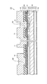
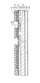
- the MOSFET 101 has a silicon carbide substrate 30, a gate insulating film 41, a gate electrode 50, an interlayer insulating film 42, a source wiring 71 (wiring), an ohmic electrode 61, and a drain electrode 62.
- Silicon carbide substrate 30 has a single crystal wafer 20 of n conductivity type (first conductivity type), a buffer layer 31 of silicon carbide and n conductivity type, and an n conductivity type of silicon carbide Drift layer 32, a pair of p type body regions 33 of p type conductivity (second conductivity type), an n + region 34 of n conductivity type, and ap + region 35 of p conductivity type Have.
- the single crystal wafer 20 has an n-type.
- the buffer layer 31 is epitaxially formed on the main surface of the single crystal wafer 20, and has n-type by being doped with a conductive impurity.
- the drift layer 32 is epitaxially formed on the buffer layer 31 and has n-type by being doped with a conductive type impurity.
- the impurity concentration per volume of the drift layer 32 is lower than the impurity concentration per volume of the buffer layer 31.
- This conductive impurity is, for example, nitrogen (N).
- the pair of p-type body regions 33 are separated from each other on the main surface (upper surface in FIG. 2) of silicon carbide substrate 30.
- the p-type body region 33 has p-type by being doped with a conductive impurity.
- the conductive impurity is, for example, aluminum (Al) or boron (B).
- Each n + region 34 is provided on the main surface of silicon carbide substrate 30 and is separated from drift layer 32 by p type body region 33.
- the impurity concentration of the n + region 34 is higher than the impurity concentration of the drift layer 32.
- P + region 35 extends from above the main surface of silicon carbide substrate 30 to p type body region 33 and is adjacent to n + region 34 on the main surface of silicon carbide substrate 30.
- the impurity concentration of p + region 35 is higher than the impurity concentration of p type body region 33.
- Gate insulating film 41 is provided directly on the main surface of silicon carbide substrate 30 and extends from the upper surface of one n + region 34 to the upper surface of the other n + region 34.
- the gate insulating film is preferably an oxide film, and is made of, for example, silicon dioxide (SiO 2 ).
- the gate electrode 50 is provided directly on the gate insulating film 41 extends over one of the n + region 34 to over the other n + region 34.
- the gate electrode 50 includes a polysilicon film 51 in contact with the gate insulating film 41, a barrier film 52 provided on the polysilicon film 51, and a metal film 53 provided on the barrier film 52.
- the polysilicon film 51 is made of polysilicon to which a conductive impurity is added.
- the thickness of polysilicon film 51 is, for example, about 400 nm.
- the barrier film 52 is made of a material that is not easily silicided as compared to the metal film 53, and for example, titanium (Ti), titanium nitride (TiN), titanium tungsten (TiW), tungsten nitride (WN), or tantalum nitride (TaW) is made from.
- the thickness of barrier film 52 is, for example, about 50 nm.
- the metal film 53 is made of a refractory metal.
- the refractory metal preferably has a melting point above 1000.degree.
- the resistivity of the metal film 53 is lower than the resistivity of the polysilicon film 51.
- the refractory metal is made of any metal of Au, Cu, Si, Ni, Mo, Ta, and W, or an alloy containing at least two of them.
- the thickness of the metal film 53 is, for example, about 50 to 400 nm.
- Interlayer insulating film 42 is provided on silicon carbide substrate 30 provided with gate insulating film 41 and gate electrode 50.
- source contact hole SH substrate contact hole
- gate contact hole GH locally exposing gate electrode 50
- Is provided in interlayer insulating film 42.
- Interlayer insulating film 42 is made of, for example, silicon dioxide (SiO 2 ).
- Source interconnection 71 is electrically connected to silicon carbide substrate 30 via source contact hole SH.
- Source interconnection 71 is electrically insulated from gate electrode 50 by interlayer insulating film 42.
- Source interconnection 71 is made of, for example, aluminum (Al).
- the source wiring 71 has a function as a pad. That is, the source wiring 71 is configured to allow wire bonding thereon.
- Ohmic electrode 61 is interposed between source interconnection 71 and silicon carbide substrate 30.
- the ohmic electrode 61 is made of a material capable of ohmic contact with the n + region 34, specifically made of silicide, for example, made of Ni x Si y (nickel silicide).
- the gate pad 72 is provided on part of the gate electrode 50.
- the gate pad 72 is electrically connected to the gate electrode 50 through the gate contact hole GH.
- Gate pad 72 is made of, for example, aluminum (Al).
- Drain electrode 62 is in contact with single crystal wafer 20 of silicon carbide substrate 30.
- Drain electrode 62 is made of a material capable of making ohmic contact with silicon carbide substrate 30, and specifically made of silicide, for example, made of Ni x Si y (nickel silicide).
- silicon carbide substrate 30 is prepared. Specifically, the following steps are performed.
- a single crystal wafer 20 of silicon carbide is prepared.
- buffer layer 31 and drift layer 32 made of silicon carbide are epitaxially grown sequentially.
- a CVD (Chemical Vapor Deposition) method can be used for this epitaxial growth.
- ion implantation is performed. Specifically, first, ion implantation for forming p-type body region 33 is performed. Specifically, for example, Al (aluminum) ions are implanted into drift layer 32 to form p type body region 33. Next, ion implantation is performed to form n + region 34. Specifically, for example, P (phosphorus) ions are implanted into p type body region 33 to form n + region 34 in p type body region 33. Further, ion implantation is performed to form p + region 35. Specifically, for example, Al ions are implanted into p type body region 33 to form p + region 35 in p type body region 33. The ion implantation can be performed, for example, by forming a mask layer made of silicon dioxide (SiO 2 ) on the main surface of the drift layer 32 and having an opening in a desired region to be subjected to the ion implantation.
- SiO 2 silicon dioxide
- activation heat treatment is performed.
- heat treatment is performed by heating to 1700 ° C. in an inert gas atmosphere such as argon and holding for 30 minutes. This activates the implanted impurities.
- silicon carbide substrate 30 is prepared.
- gate insulating film 41 is formed on silicon carbide substrate 30.
- an oxide film as the gate insulating film 41 is formed by heat treatment of heating to 1300 ° C. and holding for 60 minutes in an oxygen atmosphere. Thereafter, heat treatment using nitrogen monoxide (NO) gas as an atmosphere gas may be performed.
- NO nitrogen monoxide
- As the conditions of this heat treatment for example, conditions of holding at a temperature of 1100 ° C. or more and 1300 ° C. or less for about one hour can be adopted. By such heat treatment, nitrogen atoms are introduced into the interface region between the gate insulating film 41 and the drift layer 32.
- the formation of interface states in the interface region between the gate insulating film 41 and the drift layer 32 can be suppressed, and the channel mobility of the MOSFET 101 finally obtained can be improved.
- the NO gas instead of the NO gas, another gas capable of introducing nitrogen atoms to the interface region between the gate insulating film 41 and the drift layer 32 may be used.
- the heat treatment at a temperature higher than the temperature of this heat treatment may be performed using an argon (Ar) atmosphere in order to further suppress the formation of interface states.
- the gate electrode 50 is formed on the gate insulating film 41.
- the polysilicon film 51 in contact with the gate insulating film 41 is formed.
- Polysilicon film 51 can be formed, for example, by the CVD method.
- barrier film 52 is formed on polysilicon film 51.
- the metal film 53 is formed on the barrier film 52.
- Barrier film 52 and metal film 53 can be formed, for example, by vapor deposition.
- the gate electrode 50 is patterned.
- the patterning can be performed, for example, by photolithography and etching.
- interlayer insulating film 42 is formed on silicon carbide substrate 30 on which gate insulating film 41 and gate electrode 50 are formed.
- Interlayer insulating film 42 can be formed, for example, by the CVD method.
- source contact hole SH partially exposing silicon carbide substrate 30 is formed in interlayer insulating film 42 and gate insulating film 41. This step can be performed, for example, by photolithography and etching.
- a film 61 p is formed on silicon carbide substrate 30 in source contact hole SH.
- Film 61p is made of a material that can be ohmically contacted with silicon carbide substrate 30 by being heated, and specifically made of a material that can be silicided, such as nickel (Ni), for example. It is made from Further, in the present embodiment, on the back surface of single-crystal wafer 20 of silicon carbide substrate 30, a film 62p made of the same material as that of film 61p is formed. This step can be performed, for example, by vapor deposition.
- silicon carbide substrate 30 is heat treated.
- the temperature of the heat treatment is sufficient to promote ohmic contact between silicon carbide substrate 30 and film 61p (FIG. 8), and is preferably over 1000.degree.
- film 61 p formed on the silicon carbide substrate is heated, whereby ohmic electrode 61 is formed from film 61 p.
- drain electrode 62 is formed by heating film 62p (FIG. 8) formed on the back surface of single-crystal wafer 20 of the silicon carbide substrate.
- gate contact hole GH is formed in interlayer insulating film 42. Thereby, a part of the gate electrode 50 is exposed. This step can be performed, for example, by photolithography and etching.
- a film 70 made of metal is formed.
- This metal is, for example, aluminum.
- “metal” is a concept including not only a single metal but also an alloy.
- the film 70 is not limited to a single layer film, and may be a multilayer film.
- the multilayer film can be formed, for example, by forming a barrier film and forming an aluminum film on the barrier film.
- the material of film 70 is the same as the material of each of source interconnection 71 and gate pad 72.
- film 70 is patterned to form source interconnection 71 and gate pad 72 separated from each other, as shown in FIG. Thereby, the MOSFET 101 is obtained.
- gate electrode 50 since gate electrode 50 includes metal film 53 having a resistivity lower than that of polysilicon film 51, as compared to the case where gate electrode 50 is formed only of polysilicon film 51, Electrical resistance can be suppressed. Thus, a current path from the gate pad 72 can be formed by the gate electrode 50 having a small electric resistance.
- the gate electrode is formed only of polysilicon without using metal film 53, the resistivity of polysilicon is higher than that of the metal film, so the resistance is as low as this embodiment. If it is attempted to obtain a gate electrode having the following formula, the thickness of the gate electrode becomes excessively large. Since the gate electrode has a pattern, when the thickness is extremely large, large unevenness corresponding to this pattern will be generated on silicon carbide substrate 30. On the other hand, according to the present embodiment, the thickness of the gate electrode can be reduced by using metal film 53 having a low resistivity, and therefore, the unevenness formed on silicon carbide substrate 30 can be suppressed. .
- heat treatment of silicon carbide substrate 30 forms ohmic electrode 61 between source interconnection 71 and silicon carbide substrate 30.
- the electrical connection between source interconnection 71 and silicon carbide substrate 30 can be made more ohmic.
- the temperature of the heat treatment exceeds 1000 ° C.
- the connection between source interconnection 71 and silicon carbide substrate 30 can be made more ohmic.
- the high melting point metal which is the material of the metal film 53 has a melting point exceeding 1000 ° C.
- heat treatment at more than 1000 ° C. can be performed.
- the source wire 71 and the gate pad 72 are made of the same material.
- the MOSFET 101 can be manufactured more easily than when the material of the source wiring 71 and the material of the gate pad 72 are different. Specifically, by patterning the film 70, the source wiring 71 and the gate pad 72 can be formed simultaneously.
- the main surface of single-crystal wafer 20 facing buffer layer 31 has an off angle of 50 ° or more and 65 ° or less with respect to the ⁇ 0001 ⁇ plane. This can increase channel mobility. Further, it is preferable that an angle between the off direction of the off angle and the ⁇ 01-10> direction be 5 ° or less. Thereby, epitaxial growth on single crystal wafer 20 can be facilitated.
- the main surface preferably has an off angle of -3 ° to 5 ° with respect to the ⁇ 03-38 ⁇ plane in the ⁇ 01-10> direction, and the main surface is substantially the ⁇ 03-38 ⁇ plane. It is more preferable that Thereby, channel mobility can be further improved.
- the angle between the off orientation of the main surface and the ⁇ -2110> direction may be 5 ° or less. Thereby, epitaxial growth on single crystal wafer 20 can be facilitated.
- the main surface be a surface on the carbon surface side of silicon carbide constituting single crystal wafer 20.
- the surface on the carbon surface side is a surface in which m is negative when represented in the surface orientation (hklm). More preferably, this plane is a (0-33-8) plane. Thereby, channel mobility can be further improved.
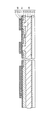
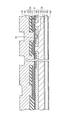
- the silicon carbide semiconductor device of the present embodiment is a MOSFET 102, more specifically, a VMOSFET (V-groove MOSFET).
- MOSFET 102 has a silicon carbide substrate 30V.
- Silicon carbide substrate 30V has trench TV, and also has p type body region 33V, n type n + region 34V, and relaxation region 36.
- Trench TV has a V-shaped shape, and penetrates n + region 34V and p-type body region 33V to reach drift layer 32.
- the preferred plane orientation of the sidewall of trench TV is the same as the preferred plane orientation of the main surface of single crystal wafer 20 (FIG. 2).
- the relaxation region 36 faces the bottom of the trench TV via the gate insulating film 41.
- the relaxation region 36 has an impurity concentration higher than the impurity concentration of the drift layer 32, and has a function of relaxing the electric field at the bottom of the trench TV.
- buffer layer 31 and drift layer 32 are epitaxially grown sequentially on the main surface of single-crystal wafer 20.
- p-type body region 33V and n + region 34V are formed.
- the p-type body region 33V can be formed by ion implantation or epitaxial growth.
- the n + region 34V can be formed by ion implantation.
- a trench TV is formed.
- the formation of the trench can be performed, for example, by photolithography and etching.
- a relaxation region 36 is formed at the bottom of the trench TV by ion implantation.
- activation heat treatment of impurities is performed.
- substantially the same steps as in FIGS. 4 to 11 of the first embodiment are performed to obtain MOSFET 102 (FIG. 12).
- gate electrode 50 has a portion disposed in trench TV. By the presence of this portion, the electrical resistance of gate electrode 50 is further suppressed by enlarging the cross-sectional area (the area in FIG. 12) of gate electrode 50 without excessively increasing the unevenness on silicon carbide substrate 30. it can.
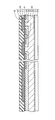
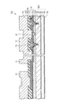
- the silicon carbide semiconductor device of the present embodiment is a MOSFET 103, and has a trench TU instead of the trench TV of the MOSFET 102 (FIG. 12).
- the trench TU has a substantially flat bottom unlike the trench TV.
- the silicon carbide semiconductor device may be a MISFET (Metal Insulator Semiconductor Field Effect Transistor) other than the MOSFET. That is, the gate insulating film 41 is not limited to the oxide.
- the silicon carbide semiconductor device is not limited to the MISFET, and may be another type of device having a gate electrode, and may be, for example, an IGBT (Insulated Gate Bipolar Transistor). Also, the wiring and the gate pad do not necessarily have to be made of the same material.
Abstract
A gate electrode (50) includes: a polysilicon film (51) in contact with a gate insulating film (41); a barrier film (52) that is provided on the polysilicon film (51); and a metal film (53), which is provided on the barrier film (52), and is composed of a high melting point metal. An interlayer insulating film (42) is disposed to cover the gate insulating film (41), and the gate electrode (50) that is provided on the gate insulating film (41). Furthermore, the interlayer insulating film (42) has a substrate contact hole (SH), from which a silicon carbide substrate (30) is partially exposed in a region in contact with the gate insulating film (41). Wiring (71) is electrically connected to the silicon carbide substrate (30) via the substrate contact hole (SH), and is electrically insulated from the gate electrode (50) by means of the interlayer insulating film (42).
Description
本発明は炭化珪素半導体装置およびその製造方法に関し、より特定的には、ゲート電極を有する炭化珪素半導体装置およびその製造方法に関するものである。
The present invention relates to a silicon carbide semiconductor device and a method of manufacturing the same, and more particularly to a silicon carbide semiconductor device having a gate electrode and a method of manufacturing the same.
特開2010-171417号公報(特許文献1)によれば、炭化珪素基板と、ゲートパッドと、ゲート電極とを有するMOSFET(Metal Oxide Semiconductor Field Effect Transistor)が開示されている。ゲート電極はポリシリコンから作られている。
JP-A-2010-171417 (Patent Document 1) discloses a MOSFET (Metal Oxide Semiconductor Field Effect Transistor) having a silicon carbide substrate, a gate pad, and a gate electrode. The gate electrode is made of polysilicon.
上記公報に記載の技術によれば、炭化珪素基板上においてゲートパッドから延びるゲート電極の電気抵抗を十分に小さくすることが困難であった。この結果、特に炭化珪素半導体装置が、半導体素子構造を各々有する複数のセルと、ゲートパッドとを有する場合、ゲートパッドから近いセルが含むゲート構造とゲートパッドとの間の抵抗値と、ゲートパッドから遠いセルが含むゲート構造とゲートパッドとの間の抵抗値とのばらつきが大きくなってしまうことがあった。
According to the technique described in the above publication, it has been difficult to sufficiently reduce the electrical resistance of the gate electrode extending from the gate pad on the silicon carbide substrate. As a result, particularly when the silicon carbide semiconductor device has a plurality of cells each having a semiconductor element structure and a gate pad, the resistance value between the gate structure and the gate pad included in the cell close to the gate pad and the gate pad In some cases, the variation in resistance between the gate structure and the gate pad included in the cell far from the cell is large.
本発明はこのような問題に対応するためになされたものであって、その目的は、ゲート電極の電気抵抗を抑制することができる炭化珪素半導体装置およびその製造方法を提供することである。
The present invention has been made to address such a problem, and it is an object of the present invention to provide a silicon carbide semiconductor device capable of suppressing the electrical resistance of a gate electrode and a method of manufacturing the same.
本発明の炭化珪素半導体装置は、炭化珪素基板と、ゲート絶縁膜と、ゲート電極と、層間絶縁膜と、配線とを有する。ゲート絶縁膜は炭化珪素基板上に設けられている。ゲート電極はゲート絶縁膜上に設けられている。ゲート電極は、ゲート絶縁膜に接するポリシリコン膜と、ポリシリコン膜上に設けられたバリア膜と、バリア膜上に設けられ高融点金属から作られた金属膜とを含む。層間絶縁膜は、ゲート絶縁膜およびゲート絶縁膜上に設けられたゲート電極を覆うように配置されている。層間絶縁膜は、ゲート絶縁膜に接する領域で炭化珪素基板を部分的に露出する基板コンタクトホールを有する。配線は、基板コンタクトホールを介して炭化珪素基板に電気的に接続され、層間絶縁膜によってゲート電極から電気的に絶縁されている。
The silicon carbide semiconductor device of the present invention has a silicon carbide substrate, a gate insulating film, a gate electrode, an interlayer insulating film, and a wiring. The gate insulating film is provided on a silicon carbide substrate. The gate electrode is provided on the gate insulating film. The gate electrode includes a polysilicon film in contact with the gate insulating film, a barrier film provided on the polysilicon film, and a metal film provided on the barrier film and made of a high melting point metal. The interlayer insulating film is arranged to cover the gate insulating film and the gate electrode provided on the gate insulating film. The interlayer insulating film has a substrate contact hole that partially exposes the silicon carbide substrate in a region in contact with the gate insulating film. The wiring is electrically connected to the silicon carbide substrate through the substrate contact hole, and is electrically isolated from the gate electrode by the interlayer insulating film.
本発明の炭化珪素半導体装置によれば、ゲート電極がポリシリコン膜に比して抵抗率の低い高融点金属膜を含むので、ゲート電極がポリシリコン膜のみから形成される場合に比して、ゲート電極の電気抵抗を抑制することができる。
According to the silicon carbide semiconductor device of the present invention, since the gate electrode includes the refractory metal film having a lower resistivity than the polysilicon film, compared to the case where the gate electrode is formed of only the polysilicon film, The electrical resistance of the gate electrode can be suppressed.
好ましくは、層間絶縁膜はゲート電極を部分的に露出するゲートコンタクトホールを有する。炭化珪素半導体装置は、ゲートコンタクトホールを介してゲート電極に電気的に接続されたゲートパッドを有する。これにより、電気抵抗の小さいゲート電極によって、ゲートパッドからの電流経路を形成することができる。より好ましくは配線およびゲートパッドは同じ材料から作られている。これにより、配線の材料とゲートパッドの材料とが異なる場合に比して、炭化珪素半導体装置をより容易に製造することができる。
Preferably, the interlayer insulating film has a gate contact hole partially exposing the gate electrode. The silicon carbide semiconductor device has a gate pad electrically connected to the gate electrode through the gate contact hole. Thus, a current path from the gate pad can be formed by the gate electrode having a small electric resistance. More preferably, the wiring and the gate pad are made of the same material. Thereby, the silicon carbide semiconductor device can be manufactured more easily than when the material of the wiring and the material of the gate pad are different.
好ましくは、高融点金属は1000℃を超える融点を有する。これにより、高融点金属から作られた金属膜が形成された後に、1000℃を超える熱処理を行うことができる。
Preferably, the refractory metal has a melting point above 1000 ° C. Thereby, after the metal film made of the high melting point metal is formed, the heat treatment can be performed at a temperature higher than 1000.degree.
上記炭化珪素基板にはトレンチが設けられていてもよく、トレンチ内にゲート電極の少なくとも一部が配置されていてもよい。これにより、ゲート電極の電気抵抗をさらに抑制することができる。
The silicon carbide substrate may be provided with a trench, and at least a part of the gate electrode may be disposed in the trench. Thereby, the electrical resistance of the gate electrode can be further suppressed.
本発明の炭化珪素半導体装置の製造方法は、以下の工程を有する。
炭化珪素基板上にゲート絶縁膜が形成される。ゲート絶縁膜上にゲート電極が形成される。ゲート電極を形成する工程は、ゲート絶縁膜に接するポリシリコン膜を形成する工程と、ポリシリコン膜上にバリア膜を形成する工程と、バリア膜上に高融点金属から作られた金属膜を形成する工程とを含む。ゲート絶縁膜およびゲート絶縁膜上に設けられたゲート電極を覆うように配置され、ゲート絶縁膜に接する領域で炭化珪素基板を部分的に露出する基板コンタクトホールを有する層間絶縁膜が形成される。基板コンタクトホールを介して炭化珪素基板に電気的に接続され、層間絶縁膜によってゲート電極から電気的に絶縁された配線が形成される。 The method for manufacturing a silicon carbide semiconductor device of the present invention has the following steps.
A gate insulating film is formed on the silicon carbide substrate. A gate electrode is formed on the gate insulating film. In the step of forming the gate electrode, the step of forming a polysilicon film in contact with the gate insulating film, the step of forming a barrier film on the polysilicon film, and the step of forming a metal film made of refractory metal on the barrier film And the step of An interlayer insulating film is formed to cover the gate insulating film and the gate electrode provided on the gate insulating film, and has a substrate contact hole that partially exposes the silicon carbide substrate in a region in contact with the gate insulating film. An interconnection electrically connected to the silicon carbide substrate through the substrate contact hole and electrically insulated from the gate electrode by the interlayer insulating film is formed.
本発明の炭化珪素半導体装置の製造方法によれば、ゲート電極がポリシリコン膜に比して抵抗率の低い高融点金属膜を含むので、ゲート電極がポリシリコン膜のみから形成される場合に比して、ゲート電極の電気抵抗を抑制することができる。
According to the method for manufacturing a silicon carbide semiconductor device of the present invention, since the gate electrode includes a refractory metal film having a resistivity lower than that of the polysilicon film, the gate electrode is formed of only the polysilicon film. Thus, the electrical resistance of the gate electrode can be suppressed.
好ましくは炭化珪素半導体装置の製造方法において、配線と炭化珪素基板との電気的接続をよりオーミックにするために、炭化珪素基板が熱処理される。これにより配線と炭化珪素基板との電気的接続をよりオーミックにすることができる。より好ましくは炭化珪素基板を熱処理する工程は、炭化珪素基板を1000℃を超える温度まで加熱する工程を含む。これにより配線と炭化珪素基板との電気的接続をよりオーミックにすることができる。
Preferably, in the method for manufacturing a silicon carbide semiconductor device, the silicon carbide substrate is heat-treated to make the electrical connection between the wiring and the silicon carbide substrate more ohmic. Thereby, the electrical connection between the wiring and the silicon carbide substrate can be made more ohmic. More preferably, the step of heat-treating the silicon carbide substrate includes the step of heating the silicon carbide substrate to a temperature exceeding 1000 ° C. Thereby, the electrical connection between the wiring and the silicon carbide substrate can be made more ohmic.
好ましくは配線を形成する工程は、ゲート電極および炭化珪素基板の各々に接する導体膜を形成する工程と、導体膜をパターニングする工程とを含む。パターニングする工程によって、配線と、ゲート電極の一部の上に設けられたゲートパッドとが形成される。これにより、配線およびゲートパッドが別個に形成される場合に比して、炭化珪素半導体装置をより容易に製造することができる。
Preferably, the step of forming the wiring includes the steps of forming a conductor film in contact with each of the gate electrode and the silicon carbide substrate, and patterning the conductor film. By the patterning process, a wire and a gate pad provided on part of the gate electrode are formed. Thereby, the silicon carbide semiconductor device can be manufactured more easily than when the wiring and the gate pad are separately formed.
上記炭化珪素基板にはトレンチが形成されてもよく、トレンチ内にゲート電極の少なくとも一部が配置されてもよい。これにより、ゲート電極の電気抵抗をさらに抑制することができる。
A trench may be formed in the silicon carbide substrate, and at least a portion of the gate electrode may be disposed in the trench. Thereby, the electrical resistance of the gate electrode can be further suppressed.
以上の説明から明らかなように、本発明の炭化珪素半導体装置によれば、電気抵抗を抑制することができる。
As apparent from the above description, according to the silicon carbide semiconductor device of the present invention, the electrical resistance can be suppressed.
以下、本発明の実施の形態について図に基づいて説明する。なお、以下の図面において、同一または相当する部分には同一の参照番号を付し、その説明は繰り返さない。また本明細書中の結晶学的な記載において、等価な個別方位を含む集合方位を<>、個別面を()、等価な個別面を含む集合面を{}で示している。また指数が負であることを示すためには、数字の上に「-」(バー)を付ける代わりに、数字の前に負の符号を付けている。
Hereinafter, embodiments of the present invention will be described based on the drawings. In the following drawings, the same or corresponding parts are denoted by the same reference numerals, and the description thereof will not be repeated. In the crystallographic description in the present specification, a collective orientation including equivalent individual orientations is indicated by <>, an individual plane is indicated by (), and a collective plane including equivalent individual planes is indicated by {}. Also, to indicate that the exponent is negative, instead of putting a "-" (bar) above the numbers, the numbers are preceded by a negative sign.
(実施の形態1)
図1および図2に示すように、本実施の形態の炭化珪素半導体装置はMOSFET101であり、より具体的にはDiMOSFET(Double implanted MOSFET)である。MOSFET101は、炭化珪素基板30と、ゲート絶縁膜41と、ゲート電極50と、層間絶縁膜42と、ソース配線71(配線)と、オーミック電極61と、ドレイン電極62とを有する。 Embodiment 1
As shown in FIGS. 1 and 2, the silicon carbide semiconductor device of the present embodiment is aMOSFET 101, more specifically, a DiMOSFET (Double implanted MOSFET). The MOSFET 101 has a silicon carbide substrate 30, a gate insulating film 41, a gate electrode 50, an interlayer insulating film 42, a source wiring 71 (wiring), an ohmic electrode 61, and a drain electrode 62.
図1および図2に示すように、本実施の形態の炭化珪素半導体装置はMOSFET101であり、より具体的にはDiMOSFET(Double implanted MOSFET)である。MOSFET101は、炭化珪素基板30と、ゲート絶縁膜41と、ゲート電極50と、層間絶縁膜42と、ソース配線71(配線)と、オーミック電極61と、ドレイン電極62とを有する。 Embodiment 1
As shown in FIGS. 1 and 2, the silicon carbide semiconductor device of the present embodiment is a
炭化珪素基板30は、導電型がn型(第1導電型)である単結晶ウエハ20と、炭化珪素からなり導電型がn型であるバッファ層31と、炭化珪素からなり導電型がn型のドリフト層32と、導電型がp型(第2導電型)の一対のp型ボディ領域33と、導電型がn型のn+領域34と、導電型がp型のp+領域35とを有する。
Silicon carbide substrate 30 has a single crystal wafer 20 of n conductivity type (first conductivity type), a buffer layer 31 of silicon carbide and n conductivity type, and an n conductivity type of silicon carbide Drift layer 32, a pair of p type body regions 33 of p type conductivity (second conductivity type), an n + region 34 of n conductivity type, and ap + region 35 of p conductivity type Have.
単結晶ウエハ20はn型を有するものである。バッファ層31は、単結晶ウエハ20の主面上にエピタキシャルに形成されており、導電型不純物がドープされることによりn型を有する。ドリフト層32は、バッファ層31上にエピタキシャルに形成されており、導電型不純物がドープされることによりn型を有する。ドリフト層32の体積当たりの不純物濃度はバッファ層31の体積当たりの不純物濃度よりも低い。この導電型不純物は、たとえば窒素(N)である。一対のp型ボディ領域33は、炭化珪素基板30の主面(図2の上面)において互いに分離されている。p型ボディ領域33は、導電型不純物がドープされることによりp型を有する。この導電型不純物は、たとえばアルミニウム(Al)またはホウ素(B)である。各n+領域34は、炭化珪素基板30の主面上に設けられており、p型ボディ領域33によってドリフト層32と分離されている。n+領域34の不純物濃度はドリフト層32の不純物濃度よりも高い。p+領域35は、炭化珪素基板30の主面上からp型ボディ領域33へと達しており、炭化珪素基板30の主面上においてn+領域34と隣接している。p+領域35の不純物濃度はp型ボディ領域33の不純物濃度よりも高い。
The single crystal wafer 20 has an n-type. The buffer layer 31 is epitaxially formed on the main surface of the single crystal wafer 20, and has n-type by being doped with a conductive impurity. The drift layer 32 is epitaxially formed on the buffer layer 31 and has n-type by being doped with a conductive type impurity. The impurity concentration per volume of the drift layer 32 is lower than the impurity concentration per volume of the buffer layer 31. This conductive impurity is, for example, nitrogen (N). The pair of p-type body regions 33 are separated from each other on the main surface (upper surface in FIG. 2) of silicon carbide substrate 30. The p-type body region 33 has p-type by being doped with a conductive impurity. The conductive impurity is, for example, aluminum (Al) or boron (B). Each n + region 34 is provided on the main surface of silicon carbide substrate 30 and is separated from drift layer 32 by p type body region 33. The impurity concentration of the n + region 34 is higher than the impurity concentration of the drift layer 32. P + region 35 extends from above the main surface of silicon carbide substrate 30 to p type body region 33 and is adjacent to n + region 34 on the main surface of silicon carbide substrate 30. The impurity concentration of p + region 35 is higher than the impurity concentration of p type body region 33.
ゲート絶縁膜41は、炭化珪素基板30の主面上に直接設けられており、一方のn+領域34の上部表面から他方のn+領域34の上部表面まで延在している。ゲート絶縁膜は、好ましくは酸化膜であり、たとえば二酸化珪素(SiO2)から作られている。
Gate insulating film 41 is provided directly on the main surface of silicon carbide substrate 30 and extends from the upper surface of one n + region 34 to the upper surface of the other n + region 34. The gate insulating film is preferably an oxide film, and is made of, for example, silicon dioxide (SiO 2 ).
ゲート電極50は、ゲート絶縁膜41上に直接設けられており、一方のn+領域34上から他方のn+領域34上にまで延在している。ゲート電極50は、ゲート絶縁膜41に接するポリシリコン膜51と、ポリシリコン膜51上に設けられたバリア膜52と、バリア膜52上に設けられた金属膜53とを含む。
The gate electrode 50 is provided directly on the gate insulating film 41 extends over one of the n + region 34 to over the other n + region 34. The gate electrode 50 includes a polysilicon film 51 in contact with the gate insulating film 41, a barrier film 52 provided on the polysilicon film 51, and a metal film 53 provided on the barrier film 52.
ポリシリコン膜51は、導電型不純物が添加されたポリシリコンから作られている。ポリシリコン膜51の厚さは、たとえば400nm程度である。
The polysilicon film 51 is made of polysilicon to which a conductive impurity is added. The thickness of polysilicon film 51 is, for example, about 400 nm.
バリア膜52は、金属膜53に比してシリサイド化されにくい材料から作られており、たとえばチタン(Ti)、窒化チタン(TiN)、チタンタングステン(TiW)、窒化タングステン(WN)、または窒化タンタル(TaW)から作られている。バリア膜52の厚さは、たとえば50nm程度である。
The barrier film 52 is made of a material that is not easily silicided as compared to the metal film 53, and for example, titanium (Ti), titanium nitride (TiN), titanium tungsten (TiW), tungsten nitride (WN), or tantalum nitride (TaW) is made from. The thickness of barrier film 52 is, for example, about 50 nm.
金属膜53は高融点金属から作られている。高融点金属は、好ましくは1000℃を超える融点を有する。金属膜53の抵抗率はポリシリコン膜51の抵抗率よりも低い。具体的には高融点金属は、Au、Cu、Si、Ni、Mo、Ta、およびWのうちのいずれかの金属、または、これらのうちの少なくとも2つを含む合金から作られている。金属膜53の厚さは、たとえば50~400nm程度である。
The metal film 53 is made of a refractory metal. The refractory metal preferably has a melting point above 1000.degree. The resistivity of the metal film 53 is lower than the resistivity of the polysilicon film 51. Specifically, the refractory metal is made of any metal of Au, Cu, Si, Ni, Mo, Ta, and W, or an alloy containing at least two of them. The thickness of the metal film 53 is, for example, about 50 to 400 nm.
層間絶縁膜42は、ゲート絶縁膜41およびゲート電極50が設けられた炭化珪素基板30上に設けられている。また層間絶縁膜42には、各n+領域34の一部とp+領域35とを露出するソースコンタクトホールSH(基板コンタクトホール)と、ゲート電極50を局所的に露出するゲートコンタクトホールGHとが設けられている。層間絶縁膜42は、たとえば二酸化珪素(SiO2)から作られている。
Interlayer insulating film 42 is provided on silicon carbide substrate 30 provided with gate insulating film 41 and gate electrode 50. In interlayer insulating film 42, source contact hole SH (substrate contact hole) exposing a portion of each n + region 34 and p + region 35, and gate contact hole GH locally exposing gate electrode 50, and Is provided. Interlayer insulating film 42 is made of, for example, silicon dioxide (SiO 2 ).
ソース配線71は、ソースコンタクトホールSHを介して炭化珪素基板30に電気的に接続されている。またソース配線71は層間絶縁膜42によってゲート電極50から電気的に絶縁されている。ソース配線71は、たとえばアルミニウム(Al)から作られている。本実施の形態においてはソース配線71はパッドとしての機能を有する。すなわちソース配線71はその上へのワイヤボンディングが可能なように構成されている。
Source interconnection 71 is electrically connected to silicon carbide substrate 30 via source contact hole SH. Source interconnection 71 is electrically insulated from gate electrode 50 by interlayer insulating film 42. Source interconnection 71 is made of, for example, aluminum (Al). In the present embodiment, the source wiring 71 has a function as a pad. That is, the source wiring 71 is configured to allow wire bonding thereon.
オーミック電極61はソース配線71と炭化珪素基板30との間に介在している。オーミック電極61は、n+領域34とオーミックコンタクト可能な材料から作られており、具体的にはシリサイドから作られており、たとえばNixSiy(ニッケルシリサイド)から作られている。
Ohmic electrode 61 is interposed between source interconnection 71 and silicon carbide substrate 30. The ohmic electrode 61 is made of a material capable of ohmic contact with the n + region 34, specifically made of silicide, for example, made of Ni x Si y (nickel silicide).
ゲートパッド72は、ゲート電極50の一部の上に設けられている。ゲートパッド72は、ゲートコンタクトホールGHを介してゲート電極50に電気的に接続されている。ゲートパッド72は、たとえばアルミニウム(Al)から作られている。
The gate pad 72 is provided on part of the gate electrode 50. The gate pad 72 is electrically connected to the gate electrode 50 through the gate contact hole GH. Gate pad 72 is made of, for example, aluminum (Al).
ドレイン電極62は、炭化珪素基板30が有する単結晶ウエハ20上に接触している。ドレイン電極62は、炭化珪素基板30とオーミックコンタクト可能な材料から作られており、具体的にはシリサイドから作られており、たとえばNixSiy(ニッケルシリサイド)から作られている。
Drain electrode 62 is in contact with single crystal wafer 20 of silicon carbide substrate 30. Drain electrode 62 is made of a material capable of making ohmic contact with silicon carbide substrate 30, and specifically made of silicide, for example, made of Ni x Si y (nickel silicide).
次にMOSFET101の製造方法について説明する。
図3に示すように、炭化珪素基板30が準備される。具体的には、以下の工程が行われる。 Next, a method of manufacturing theMOSFET 101 will be described.
As shown in FIG. 3,silicon carbide substrate 30 is prepared. Specifically, the following steps are performed.
図3に示すように、炭化珪素基板30が準備される。具体的には、以下の工程が行われる。 Next, a method of manufacturing the
As shown in FIG. 3,
まず炭化珪素の単結晶ウエハ20が準備される。次に、単結晶ウエハ20の主面上に、炭化珪素からなるバッファ層31およびドリフト層32が順次エピタキシャル成長される。このエピタキシャル成長のためには、たとえばCVD(Chemical Vapor Deposition)法を用いることができる。
First, a single crystal wafer 20 of silicon carbide is prepared. Next, on the main surface of single crystal wafer 20, buffer layer 31 and drift layer 32 made of silicon carbide are epitaxially grown sequentially. For this epitaxial growth, for example, a CVD (Chemical Vapor Deposition) method can be used.
次にイオン注入が行われる。具体的にはまずp型ボディ領域33を形成するためのイオン注入が実施される。具体的には、たとえばAl(アルミニウム)イオンがドリフト層32に注入されることにより、p型ボディ領域33が形成される。次に、n+領域34を形成するためのイオン注入が実施される。具体的には、たとえばP(リン)イオンがp型ボディ領域33に注入されることにより、p型ボディ領域33内にn+領域34が形成される。さらに、p+領域35を形成するためのイオン注入が実施される。具体的には、たとえばAlイオンがp型ボディ領域33に注入されることにより、p型ボディ領域33内にp+領域35が形成される。上記イオン注入は、たとえばドリフト層32の主面上に二酸化珪素(SiO2)からなり、イオン注入を実施すべき所望の領域に開口を有するマスク層を形成して実施することができる。
Next, ion implantation is performed. Specifically, first, ion implantation for forming p-type body region 33 is performed. Specifically, for example, Al (aluminum) ions are implanted into drift layer 32 to form p type body region 33. Next, ion implantation is performed to form n + region 34. Specifically, for example, P (phosphorus) ions are implanted into p type body region 33 to form n + region 34 in p type body region 33. Further, ion implantation is performed to form p + region 35. Specifically, for example, Al ions are implanted into p type body region 33 to form p + region 35 in p type body region 33. The ion implantation can be performed, for example, by forming a mask layer made of silicon dioxide (SiO 2 ) on the main surface of the drift layer 32 and having an opening in a desired region to be subjected to the ion implantation.
次に活性化熱処理が実施される。たとえば、アルゴンなどの不活性ガス雰囲気中において1700℃に加熱し、30分間保持する熱処理が実施される。これにより、注入されていた不純物が活性化される。
Next, activation heat treatment is performed. For example, heat treatment is performed by heating to 1700 ° C. in an inert gas atmosphere such as argon and holding for 30 minutes. This activates the implanted impurities.
以上により、炭化珪素基板30が準備される。
図4に示すように、炭化珪素基板30上にゲート絶縁膜41が形成される。具体的には、酸素雰囲気中において1300℃に加熱して60分間保持する熱処理により、ゲート絶縁膜41としての酸化膜が形成される。この後、雰囲気ガスとして一酸化窒素(NO)ガスを用いた熱処理が行われてもよい。この熱処理の条件としては、たとえば1100℃以上1300℃以下の温度で1時間程度保持する条件を採用することができる。このような熱処理により、ゲート絶縁膜41とドリフト層32との界面領域に窒素原子が導入される。これにより、ゲート絶縁膜41とドリフト層32との界面領域における界面準位の形成が抑制され、最終的に得られるMOSFET101のチャネル移動度を向上させることができる。なおNOガスの代わりに、ゲート絶縁膜41とドリフト層32との界面領域に窒素原子を導入することが可能な他のガスが用いられてもよい。また窒素原子導入のための熱処理後、界面準位の形成をさらに抑制するために、この熱処理の温度よりも高い温度での熱処理をアルゴン(Ar)雰囲気を用いて行ってもよい。 Thus,silicon carbide substrate 30 is prepared.
As shown in FIG. 4,gate insulating film 41 is formed on silicon carbide substrate 30. Specifically, an oxide film as the gate insulating film 41 is formed by heat treatment of heating to 1300 ° C. and holding for 60 minutes in an oxygen atmosphere. Thereafter, heat treatment using nitrogen monoxide (NO) gas as an atmosphere gas may be performed. As the conditions of this heat treatment, for example, conditions of holding at a temperature of 1100 ° C. or more and 1300 ° C. or less for about one hour can be adopted. By such heat treatment, nitrogen atoms are introduced into the interface region between the gate insulating film 41 and the drift layer 32. Thus, the formation of interface states in the interface region between the gate insulating film 41 and the drift layer 32 can be suppressed, and the channel mobility of the MOSFET 101 finally obtained can be improved. Note that, instead of the NO gas, another gas capable of introducing nitrogen atoms to the interface region between the gate insulating film 41 and the drift layer 32 may be used. After the heat treatment for introducing nitrogen atoms, the heat treatment at a temperature higher than the temperature of this heat treatment may be performed using an argon (Ar) atmosphere in order to further suppress the formation of interface states.
図4に示すように、炭化珪素基板30上にゲート絶縁膜41が形成される。具体的には、酸素雰囲気中において1300℃に加熱して60分間保持する熱処理により、ゲート絶縁膜41としての酸化膜が形成される。この後、雰囲気ガスとして一酸化窒素(NO)ガスを用いた熱処理が行われてもよい。この熱処理の条件としては、たとえば1100℃以上1300℃以下の温度で1時間程度保持する条件を採用することができる。このような熱処理により、ゲート絶縁膜41とドリフト層32との界面領域に窒素原子が導入される。これにより、ゲート絶縁膜41とドリフト層32との界面領域における界面準位の形成が抑制され、最終的に得られるMOSFET101のチャネル移動度を向上させることができる。なおNOガスの代わりに、ゲート絶縁膜41とドリフト層32との界面領域に窒素原子を導入することが可能な他のガスが用いられてもよい。また窒素原子導入のための熱処理後、界面準位の形成をさらに抑制するために、この熱処理の温度よりも高い温度での熱処理をアルゴン(Ar)雰囲気を用いて行ってもよい。 Thus,
As shown in FIG. 4,
次にゲート絶縁膜41上にゲート電極50が形成される。具体的には、まずゲート絶縁膜41に接するポリシリコン膜51が形成される。ポリシリコン膜51は、たとえばCVD法により成膜され得る。次にポリシリコン膜51上にバリア膜52が形成される。次にバリア膜52上に金属膜53が形成される。バリア膜52および金属膜53は、たとえば蒸着法により成膜され得る。
Next, the gate electrode 50 is formed on the gate insulating film 41. Specifically, first, the polysilicon film 51 in contact with the gate insulating film 41 is formed. Polysilicon film 51 can be formed, for example, by the CVD method. Next, barrier film 52 is formed on polysilicon film 51. Next, the metal film 53 is formed on the barrier film 52. Barrier film 52 and metal film 53 can be formed, for example, by vapor deposition.
図5に示すように、ゲート電極50がパターニングされる。パターニングは、たとえば、フォトリソグラフィおよびエッチングにより行うことができる。
As shown in FIG. 5, the gate electrode 50 is patterned. The patterning can be performed, for example, by photolithography and etching.
図6に示すように、ゲート絶縁膜41およびゲート電極50が形成された炭化珪素基板30上に、層間絶縁膜42が形成される。層間絶縁膜42は、たとえばCVD法により形成され得る。
As shown in FIG. 6, interlayer insulating film 42 is formed on silicon carbide substrate 30 on which gate insulating film 41 and gate electrode 50 are formed. Interlayer insulating film 42 can be formed, for example, by the CVD method.
図7に示すように、層間絶縁膜42およびゲート絶縁膜41に、炭化珪素基板30を部分的に露出するソースコンタクトホールSHが形成される。この工程は、たとえば、フォトリソグラフィおよびエッチングにより行うことができる。
As shown in FIG. 7, source contact hole SH partially exposing silicon carbide substrate 30 is formed in interlayer insulating film 42 and gate insulating film 41. This step can be performed, for example, by photolithography and etching.
図8に示すように、ソースコンタクトホールSH内において、炭化珪素基板30上に膜61pが形成される。膜61pは、加熱されることによって炭化珪素基板30とのオーミック接触が可能となるような材料から作られており、具体的にはシリサイド化可能な材料から作られており、たとえばニッケル(Ni)から作られている。また本実施の形態においては、炭化珪素基板30が有する単結晶ウエハ20の裏面上に、膜61pの材料と同様の材料から作られた膜62pが形成される。この工程は、たとえば蒸着法により行い得る。
As shown in FIG. 8, a film 61 p is formed on silicon carbide substrate 30 in source contact hole SH. Film 61p is made of a material that can be ohmically contacted with silicon carbide substrate 30 by being heated, and specifically made of a material that can be silicided, such as nickel (Ni), for example. It is made from Further, in the present embodiment, on the back surface of single-crystal wafer 20 of silicon carbide substrate 30, a film 62p made of the same material as that of film 61p is formed. This step can be performed, for example, by vapor deposition.
図9に示すように、炭化珪素基板30が熱処理される。熱処理の温度は、炭化珪素基板30と膜61p(図8)とのオーミック接触が促進されるのに十分なものとされ、好ましくは1000℃超である。この熱処理により、炭化珪素基板上に形成された膜61pが加熱されることで、膜61pからオーミック電極61が形成される。また炭化珪素基板が有する単結晶ウエハ20の裏面上に形成された膜62p(図8)が加熱されることで、ドレイン電極62が形成される。
As shown in FIG. 9, silicon carbide substrate 30 is heat treated. The temperature of the heat treatment is sufficient to promote ohmic contact between silicon carbide substrate 30 and film 61p (FIG. 8), and is preferably over 1000.degree. By this heat treatment, film 61 p formed on the silicon carbide substrate is heated, whereby ohmic electrode 61 is formed from film 61 p. In addition, drain electrode 62 is formed by heating film 62p (FIG. 8) formed on the back surface of single-crystal wafer 20 of the silicon carbide substrate.
図10に示すように、層間絶縁膜42にゲートコンタクトホールGHが形成される。これにより、ゲート電極50の一部が露出される。この工程は、たとえば、フォトリソグラフィおよびエッチングにより行うことができる。
As shown in FIG. 10, gate contact hole GH is formed in interlayer insulating film 42. Thereby, a part of the gate electrode 50 is exposed. This step can be performed, for example, by photolithography and etching.
図11に示すように、金属から作られた膜70が形成される。この金属は、たとえばアルミニウムである。なお本明細書において「金属」とは、単体の金属だけでなく、合金も含む概念である。また膜70は単層膜に限られず、多層膜であってもよい。この多層膜は、たとえば、バリア膜の形成と、このバリア膜上へのアルミニウム膜の形成とによって形成され得る。また膜70の材料は、ソース配線71およびゲートパッド72の各々の材料と同じである。
As shown in FIG. 11, a film 70 made of metal is formed. This metal is, for example, aluminum. In the present specification, “metal” is a concept including not only a single metal but also an alloy. The film 70 is not limited to a single layer film, and may be a multilayer film. The multilayer film can be formed, for example, by forming a barrier film and forming an aluminum film on the barrier film. Also, the material of film 70 is the same as the material of each of source interconnection 71 and gate pad 72.
次に膜70がパターニングされることによって、図2に示すように、互いに分離されたソース配線71およびゲートパッド72が形成される。これによりMOSFET101が得られる。
Next, film 70 is patterned to form source interconnection 71 and gate pad 72 separated from each other, as shown in FIG. Thereby, the MOSFET 101 is obtained.
本実施の形態によれば、ゲート電極50がポリシリコン膜51に比して抵抗率の低い金属膜53を含むので、ゲート電極50がポリシリコン膜51のみから形成される場合に比して、電気抵抗を抑制することができる。これにより、電気抵抗の小さいゲート電極50によって、ゲートパッド72からの電流経路を形成することができる。
According to the present embodiment, since gate electrode 50 includes metal film 53 having a resistivity lower than that of polysilicon film 51, as compared to the case where gate electrode 50 is formed only of polysilicon film 51, Electrical resistance can be suppressed. Thus, a current path from the gate pad 72 can be formed by the gate electrode 50 having a small electric resistance.
なお仮に金属膜53を用いずにポリシリコンのみでゲート電極が形成される場合、ポリシリコンの抵抗率が金属膜の抵抗率に比して大きいことから、本実施の形態と同程度に低い抵抗を有するゲート電極を得ようとすると、ゲート電極の厚さが過度に大きくなってしまう。ゲート電極はパターンを有するので、その厚さが極端に大きい場合、このパターンに対応した大きな凹凸が炭化珪素基板30上に生じてしまう。これに対して本実施の形態によれば、抵抗率の低い金属膜53を用いることでゲート電極の厚さを小さくすることができるので、炭化珪素基板30上に生じる凹凸を抑制することができる。
If the gate electrode is formed only of polysilicon without using metal film 53, the resistivity of polysilicon is higher than that of the metal film, so the resistance is as low as this embodiment. If it is attempted to obtain a gate electrode having the following formula, the thickness of the gate electrode becomes excessively large. Since the gate electrode has a pattern, when the thickness is extremely large, large unevenness corresponding to this pattern will be generated on silicon carbide substrate 30. On the other hand, according to the present embodiment, the thickness of the gate electrode can be reduced by using metal film 53 having a low resistivity, and therefore, the unevenness formed on silicon carbide substrate 30 can be suppressed. .
また炭化珪素基板30が熱処理されることで、ソース配線71と炭化珪素基板30との間にオーミック電極61が形成される。これによりソース配線71と炭化珪素基板30との電気的接続をよりオーミックにすることができる。好ましくは熱処理の温度は1000℃を超える。これによりソース配線71と炭化珪素基板30との接続をよりオーミックにすることができる。
Further, heat treatment of silicon carbide substrate 30 forms ohmic electrode 61 between source interconnection 71 and silicon carbide substrate 30. Thereby, the electrical connection between source interconnection 71 and silicon carbide substrate 30 can be made more ohmic. Preferably, the temperature of the heat treatment exceeds 1000 ° C. Thereby, the connection between source interconnection 71 and silicon carbide substrate 30 can be made more ohmic.
好ましくは、金属膜53の材料である高融点金属は、1000℃を超える融点を有する。これにより、金属膜53が形成された後に、1000℃を超える熱処理を行うことができる。
Preferably, the high melting point metal which is the material of the metal film 53 has a melting point exceeding 1000 ° C. Thus, after the metal film 53 is formed, heat treatment at more than 1000 ° C. can be performed.
また本実施の形態においては、ソース配線71およびゲートパッド72は同じ材料から作られている。これにより、ソース配線71の材料とゲートパッド72の材料とが異なる場合に比して、MOSFET101をより容易に製造することができる。具体的には、膜70をパターニングすることによって、ソース配線71と、ゲートパッド72とを同時に形成することができる。
Further, in the present embodiment, the source wire 71 and the gate pad 72 are made of the same material. Thus, the MOSFET 101 can be manufactured more easily than when the material of the source wiring 71 and the material of the gate pad 72 are different. Specifically, by patterning the film 70, the source wiring 71 and the gate pad 72 can be formed simultaneously.
なお単結晶ウエハ20の、バッファ層31に面する主面は、{0001}面に対して50°以上65°以下のオフ角を有することが好ましい。これによりチャネル移動度を高めることができる。またこのオフ角のオフ方位と<01-10>方向とのなす角は5°以下となっていることが好ましい。これにより、単結晶ウエハ20上へのエピタキシャル成長を容易にすることができる。
Preferably, the main surface of single-crystal wafer 20 facing buffer layer 31 has an off angle of 50 ° or more and 65 ° or less with respect to the {0001} plane. This can increase channel mobility. Further, it is preferable that an angle between the off direction of the off angle and the <01-10> direction be 5 ° or less. Thereby, epitaxial growth on single crystal wafer 20 can be facilitated.
さらに、上記主面の、<01-10>方向における{03-38}面に対するオフ角は-3°以上5°以下であることが好ましく、この主面は実質的に{03-38}面であることがより好ましい。これにより、チャネル移動度を一層向上させることができる。
Furthermore, the main surface preferably has an off angle of -3 ° to 5 ° with respect to the {03-38} plane in the <01-10> direction, and the main surface is substantially the {03-38} plane. It is more preferable that Thereby, channel mobility can be further improved.
上記主面のオフ方位と<-2110>方向とのなす角は5°以下となっていてもよい。これにより、単結晶ウエハ20上へのエピタキシャル成長を容易にすることができる。
The angle between the off orientation of the main surface and the <-2110> direction may be 5 ° or less. Thereby, epitaxial growth on single crystal wafer 20 can be facilitated.
さらに、上記主面は、単結晶ウエハ20を構成する炭化珪素のカーボン面側の面であることが好ましい。カーボン面側の面とは、面方位(hklm)で表された場合にmが負である面である。より好ましくはこの面は(0-33-8)面である。これにより、チャネル移動度をさらに向上させることができる。
Furthermore, it is preferable that the main surface be a surface on the carbon surface side of silicon carbide constituting single crystal wafer 20. The surface on the carbon surface side is a surface in which m is negative when represented in the surface orientation (hklm). More preferably, this plane is a (0-33-8) plane. Thereby, channel mobility can be further improved.
(実施の形態2)
図12に示すように、本実施の形態の炭化珪素半導体装置はMOSFET102であり、より具体的にはVMOSFET(V-groove MOSFET)である。MOSFET102は炭化珪素基板30Vを有する。炭化珪素基板30Vは、トレンチTVを有し、またp型ボディ領域33Vと、n型のn+領域34Vと、緩和領域36とを有する。トレンチTVは、V字状の形状を有し、n+領域34Vおよびp型ボディ領域33Vを貫通してドリフト層32内に達している。トレンチTVの側壁の好適な面方位は、単結晶ウエハ20(図2)の主面の好適な面方位と同様である。緩和領域36は、ゲート絶縁膜41を介して、トレンチTVの底部に面している。緩和領域36は、ドリフト層32の不純物濃度よりも高い不純物濃度を有し、トレンチTV底部における電界を緩和する機能を有する。 Second Embodiment
As shown in FIG. 12, the silicon carbide semiconductor device of the present embodiment is aMOSFET 102, more specifically, a VMOSFET (V-groove MOSFET). MOSFET 102 has a silicon carbide substrate 30V. Silicon carbide substrate 30V has trench TV, and also has p type body region 33V, n type n + region 34V, and relaxation region 36. Trench TV has a V-shaped shape, and penetrates n + region 34V and p-type body region 33V to reach drift layer 32. The preferred plane orientation of the sidewall of trench TV is the same as the preferred plane orientation of the main surface of single crystal wafer 20 (FIG. 2). The relaxation region 36 faces the bottom of the trench TV via the gate insulating film 41. The relaxation region 36 has an impurity concentration higher than the impurity concentration of the drift layer 32, and has a function of relaxing the electric field at the bottom of the trench TV.
図12に示すように、本実施の形態の炭化珪素半導体装置はMOSFET102であり、より具体的にはVMOSFET(V-groove MOSFET)である。MOSFET102は炭化珪素基板30Vを有する。炭化珪素基板30Vは、トレンチTVを有し、またp型ボディ領域33Vと、n型のn+領域34Vと、緩和領域36とを有する。トレンチTVは、V字状の形状を有し、n+領域34Vおよびp型ボディ領域33Vを貫通してドリフト層32内に達している。トレンチTVの側壁の好適な面方位は、単結晶ウエハ20(図2)の主面の好適な面方位と同様である。緩和領域36は、ゲート絶縁膜41を介して、トレンチTVの底部に面している。緩和領域36は、ドリフト層32の不純物濃度よりも高い不純物濃度を有し、トレンチTV底部における電界を緩和する機能を有する。 Second Embodiment
As shown in FIG. 12, the silicon carbide semiconductor device of the present embodiment is a
次にMOSFET102の製造方法について、以下に説明する。
図13に示すように、実施の形態1と同様に、単結晶ウエハ20の主面上にバッファ層31およびドリフト層32が順次エピタキシャル成長される。次にp型ボディ領域33Vおよびn+領域34Vが形成される。p型ボディ領域33Vは、イオン注入またはエピタキシャル成長によって形成し得る。n+領域34Vはイオン注入によって形成し得る。 Next, a method of manufacturing theMOSFET 102 will be described below.
As shown in FIG. 13, as in the first embodiment,buffer layer 31 and drift layer 32 are epitaxially grown sequentially on the main surface of single-crystal wafer 20. Next, p-type body region 33V and n + region 34V are formed. The p-type body region 33V can be formed by ion implantation or epitaxial growth. The n + region 34V can be formed by ion implantation.
図13に示すように、実施の形態1と同様に、単結晶ウエハ20の主面上にバッファ層31およびドリフト層32が順次エピタキシャル成長される。次にp型ボディ領域33Vおよびn+領域34Vが形成される。p型ボディ領域33Vは、イオン注入またはエピタキシャル成長によって形成し得る。n+領域34Vはイオン注入によって形成し得る。 Next, a method of manufacturing the
As shown in FIG. 13, as in the first embodiment,
図14に示すように、トレンチTVが形成される。トレンチの形成は、たとえば、フォトリソグラフィおよびエッチングにより行うことができる。次にトレンチTVの底部にイオン注入により緩和領域36が形成される。次に不純物の活性化熱処理が実施される。次に、実施の形態1の図4~図11とほぼ同様の工程が行われることで、MOSFET102(図12)が得られる。
As shown in FIG. 14, a trench TV is formed. The formation of the trench can be performed, for example, by photolithography and etching. Next, a relaxation region 36 is formed at the bottom of the trench TV by ion implantation. Next, activation heat treatment of impurities is performed. Next, substantially the same steps as in FIGS. 4 to 11 of the first embodiment are performed to obtain MOSFET 102 (FIG. 12).
なお、上記以外の構成については、上述した実施の形態1の構成とほぼ同じであるため、同一または対応する要素について同一の符号を付し、その説明を繰り返さない。
The configuration other than the above is substantially the same as the configuration of the first embodiment described above, so the same or corresponding elements are denoted by the same reference characters and description thereof will not be repeated.
本実施の形態によれば、ゲート電極50は、トレンチTV内に配置された部分を有する。この部分の存在によって、炭化珪素基板30上に凹凸を過度に大きくすることなく、ゲート電極50の断面積(図12における面積)を大きくすることでゲート電極50の電気抵抗をさらに抑制することができる。
According to the present embodiment, gate electrode 50 has a portion disposed in trench TV. By the presence of this portion, the electrical resistance of gate electrode 50 is further suppressed by enlarging the cross-sectional area (the area in FIG. 12) of gate electrode 50 without excessively increasing the unevenness on silicon carbide substrate 30. it can.
(実施の形態3)
図15に示すように、本実施の形態の炭化珪素半導体装置はMOSFET103であり、MOSFET102(図12)のトレンチTVの代わりにトレンチTUを有する。トレンチTUはトレンチTVと異なり、ほぼ平坦な底部を有する。 Third Embodiment
As shown in FIG. 15, the silicon carbide semiconductor device of the present embodiment is aMOSFET 103, and has a trench TU instead of the trench TV of the MOSFET 102 (FIG. 12). The trench TU has a substantially flat bottom unlike the trench TV.
図15に示すように、本実施の形態の炭化珪素半導体装置はMOSFET103であり、MOSFET102(図12)のトレンチTVの代わりにトレンチTUを有する。トレンチTUはトレンチTVと異なり、ほぼ平坦な底部を有する。 Third Embodiment
As shown in FIG. 15, the silicon carbide semiconductor device of the present embodiment is a
なお、上記以外の構成については、上述した実施の形態2の構成とほぼ同じであるため、同一または対応する要素について同一の符号を付し、その説明を繰り返さない。
The configuration other than the above is substantially the same as the configuration of the second embodiment described above, so the same or corresponding elements are denoted by the same reference characters and description thereof will not be repeated.
上記MOSFET101~103の各々において、n型とp型とが入れ替えられてもよい。また炭化珪素半導体装置は、MOSFET以外のMISFET(Metal Insulator Semiconductor Field Effect Transistor)であってもよい。すなわちゲート絶縁膜41は酸化物に限定されるものではない。また炭化珪素半導体装置はMISFETに限定されるものではなく、ゲート電極を有する他の種類の装置であってもよく、たとえばIGBT(Insulated Gate Bipolar Transistor)であってもよい。また配線とゲートパッドとは、必ずしも同じ材料から作られている必要はない。
In each of the MOSFETs 101 to 103, n-type and p-type may be interchanged. The silicon carbide semiconductor device may be a MISFET (Metal Insulator Semiconductor Field Effect Transistor) other than the MOSFET. That is, the gate insulating film 41 is not limited to the oxide. The silicon carbide semiconductor device is not limited to the MISFET, and may be another type of device having a gate electrode, and may be, for example, an IGBT (Insulated Gate Bipolar Transistor). Also, the wiring and the gate pad do not necessarily have to be made of the same material.
今回開示された実施の形態はすべての点で例示であって、制限的なものではないと考えられるべきである。本発明の範囲は上記した説明ではなくて請求の範囲によって示され、請求の範囲と均等の意味、および範囲内でのすべての変更が含まれることが意図される。
It should be understood that the embodiments disclosed herein are illustrative in all respects and not restrictive. The scope of the present invention is shown not by the above description but by the scope of claims, and is intended to include meanings equivalent to the scope of claims and all modifications within the scope.
20 単結晶ウエハ、30,30V 炭化珪素基板、31 バッファ層、32 ドリフト層、33,33V p型ボディ領域、34,34V n+領域、35 p+領域、36 緩和領域、41 ゲート絶縁膜、42 層間絶縁膜、50 ゲート電極、51 ポリシリコン膜、52 バリア膜、53 金属膜、61 オーミック電極、62 ドレイン電極、71 ソース配線、72 ゲートパッド、101~103 MOSFET(半導体装置)、GH ゲートコンタクトホール、SH ソースコンタクトホール(基板コンタクトホール)、TU,TV トレンチ。
20 single crystal wafer, 30, 30 V silicon carbide substrate, 31 buffer layer, 32 drift layer, 33, 33 V p-type body region, 34, 34 V n + region, 35 p + region, 36 relaxation region, 41 gate insulating film, 42 Interlayer insulating film, 50 gate electrode, 51 polysilicon film, 52 barrier film, 53 metal film, 61 ohmic electrode, 62 drain electrode, 71 source wiring, 72 gate pad, 101 to 103 MOSFET (semiconductor device), GH gate contact hole , SH source contact hole (substrate contact hole), TU, TV trench.
Claims (10)
- 炭化珪素基板(30、30V)と、
前記炭化珪素基板上に設けられたゲート絶縁膜(41)と、
前記ゲート絶縁膜上に設けられたゲート電極(50)とを備え、
前記ゲート電極は、前記ゲート絶縁膜に接するポリシリコン膜(51)と、前記ポリシリコン膜上に設けられたバリア膜(52)と、前記バリア膜上に設けられ高融点金属から作られた金属膜(53)とを含み、さらに
前記ゲート絶縁膜および前記ゲート絶縁膜上に設けられた前記ゲート電極を覆うように配置され、前記ゲート絶縁膜に接する領域で前記炭化珪素基板を部分的に露出する基板コンタクトホール(SH)を有する層間絶縁膜(42)と、
前記基板コンタクトホールを介して前記炭化珪素基板に電気的に接続され、前記層間絶縁膜によって前記ゲート電極から電気的に絶縁された配線(71)とを備える、炭化珪素半導体装置(101~103)。 Silicon carbide substrate (30, 30 V),
A gate insulating film (41) provided on the silicon carbide substrate;
And a gate electrode (50) provided on the gate insulating film,
The gate electrode is formed of a polysilicon film (51) in contact with the gate insulating film, a barrier film (52) provided on the polysilicon film, and a metal provided on the barrier film and made of a refractory metal Film (53), and further disposed to cover the gate insulating film and the gate electrode provided on the gate insulating film, and partially expose the silicon carbide substrate in a region in contact with the gate insulating film. An interlayer insulating film (42) having a substrate contact hole (SH)
A silicon carbide semiconductor device (101 to 103) comprising: a wire (71) electrically connected to the silicon carbide substrate through the substrate contact hole and electrically isolated from the gate electrode by the interlayer insulating film. . - 前記層間絶縁膜は前記ゲート電極を部分的に露出するゲートコンタクトホール(GH)を有し、
前記ゲートコンタクトホールを介して前記ゲート電極に電気的に接続されたゲートパッド(72)をさらに備える、請求項1に記載の炭化珪素半導体装置。 The interlayer insulating film has a gate contact hole (GH) partially exposing the gate electrode,
The silicon carbide semiconductor device according to claim 1, further comprising a gate pad (72) electrically connected to said gate electrode through said gate contact hole. - 前記配線および前記ゲートパッドは同じ材料から作られている、請求項2に記載の炭化珪素半導体装置。 The silicon carbide semiconductor device according to claim 2, wherein the wiring and the gate pad are made of the same material.
- 前記高融点金属は1000℃を超える融点を有する、請求項1~3のいずれか1項に記載の炭化珪素半導体装置。 The silicon carbide semiconductor device according to any one of claims 1 to 3, wherein the refractory metal has a melting point exceeding 1000 属 C.
- 前記炭化珪素基板(30V)にトレンチ(TU、TV)が設けられており、前記トレンチ内に前記ゲート電極の少なくとも一部が配置されている、請求項1~4のいずれか1項に記載の炭化珪素半導体装置(102、103)。 A trench (TU, TV) is provided in the silicon carbide substrate (30 V), and at least a part of the gate electrode is disposed in the trench. Silicon carbide semiconductor device (102, 103).
- 炭化珪素基板(30、30V)上にゲート絶縁膜(41)を形成する工程と、
前記ゲート絶縁膜上にゲート電極(50)を形成する工程と備え、
前記ゲート電極を形成する工程は、前記ゲート絶縁膜に接するポリシリコン膜(51)を形成する工程と、前記ポリシリコン膜上にバリア膜(52)を形成する工程と、前記バリア膜上に高融点金属から作られた金属膜(53)を形成する工程とを含み、さらに
前記ゲート絶縁膜および前記ゲート絶縁膜上に設けられた前記ゲート電極を覆うように配置され、前記ゲート絶縁膜に接する領域で前記炭化珪素基板を部分的に露出する基板コンタクトホール(SH)を有する層間絶縁膜(42)を形成する工程と、
前記基板コンタクトホールを介して前記炭化珪素基板に電気的に接続され、前記層間絶縁膜によって前記ゲート電極から電気的に絶縁された配線(71)を形成する工程とを備える、炭化珪素半導体装置(101~103)の製造方法。 Forming a gate insulating film (41) on a silicon carbide substrate (30, 30 V);
Forming a gate electrode (50) on the gate insulating film;
The step of forming the gate electrode includes a step of forming a polysilicon film (51) in contact with the gate insulating film, a step of forming a barrier film (52) on the polysilicon film, and a step of forming a gate film on the barrier film. And a step of forming a metal film (53) made of a melting point metal, and further disposed so as to cover the gate insulating film and the gate electrode provided on the gate insulating film, and in contact with the gate insulating film Forming an interlayer insulating film (42) having a substrate contact hole (SH) partially exposing the silicon carbide substrate in a region;
Forming a wire (71) electrically connected to the silicon carbide substrate through the substrate contact hole and electrically insulated from the gate electrode by the interlayer insulating film ((7) 101 to 103). - 前記配線と前記炭化珪素基板との電気的接続をよりオーミックにするために前記炭化珪素基板を熱処理する工程をさらに備える、請求項6に記載の炭化珪素半導体装置の製造方法。 7. The method for manufacturing a silicon carbide semiconductor device according to claim 6, further comprising the step of heat-treating said silicon carbide substrate to make the electrical connection between said wiring and said silicon carbide substrate more ohmic.
- 前記炭化珪素基板を熱処理する工程は、前記炭化珪素基板を1000℃を超える温度まで加熱する工程を含む、請求項7に記載の炭化珪素半導体装置の製造方法。 The method of manufacturing a silicon carbide semiconductor device according to claim 7, wherein the step of heat-treating said silicon carbide substrate includes the step of heating said silicon carbide substrate to a temperature exceeding 1000 ° C.
- 前記配線を形成する工程は、前記ゲート電極および前記炭化珪素基板の各々に接する導体膜(70)を形成する工程と、前記導体膜をパターニングする工程とを含み、前記パターニングする工程によって、前記配線と、前記ゲート電極の一部の上に設けられたゲートパッド(72)とが形成される、請求項6~8のいずれか1項に記載の炭化珪素半導体装置の製造方法。 The step of forming the wire includes a step of forming a conductor film (70) in contact with each of the gate electrode and the silicon carbide substrate, and a step of patterning the conductor film, and the step of forming the wire The method for manufacturing a silicon carbide semiconductor device according to any one of claims 6 to 8, wherein a gate pad (72) provided on part of the gate electrode is formed.
- 前記炭化珪素基板(30V)にトレンチ(TU、TV)を形成する工程をさらに備え、前記トレンチ内に前記ゲート電極の少なくとも一部が配置される、請求項6~9のいずれか1項に記載の炭化珪素半導体装置(102、103)の製造方法。 The method according to any one of claims 6 to 9, further comprising the step of forming a trench (TU, TV) in the silicon carbide substrate (30 V), wherein at least a part of the gate electrode is disposed in the trench. Method of manufacturing a silicon carbide semiconductor device (102, 103) according to
Priority Applications (3)
| Application Number | Priority Date | Filing Date | Title |
|---|---|---|---|
| EP12800187.2A EP2722892A4 (en) | 2011-06-15 | 2012-05-29 | Silicon carbide semiconductor device and method for manufacturing same |
| CN201280023455.4A CN103548144A (en) | 2011-06-15 | 2012-05-29 | Silicon carbide semiconductor device and method for manufacturing same |
| KR1020137027717A KR20140021609A (en) | 2011-06-15 | 2012-05-29 | Silicon carbide semiconductor device and method for manufacturing same |
Applications Claiming Priority (2)
| Application Number | Priority Date | Filing Date | Title |
|---|---|---|---|
| JP2011132784A JP2013004636A (en) | 2011-06-15 | 2011-06-15 | Silicon carbide semiconductor device and manufacturing method of the same |
| JP2011-132784 | 2011-06-15 |
Publications (1)
| Publication Number | Publication Date |
|---|---|
| WO2012172965A1 true WO2012172965A1 (en) | 2012-12-20 |
Family
ID=47352981
Family Applications (1)
| Application Number | Title | Priority Date | Filing Date |
|---|---|---|---|
| PCT/JP2012/063722 WO2012172965A1 (en) | 2011-06-15 | 2012-05-29 | Silicon carbide semiconductor device and method for manufacturing same |
Country Status (7)
| Country | Link |
|---|---|
| US (1) | US20120319134A1 (en) |
| EP (1) | EP2722892A4 (en) |
| JP (1) | JP2013004636A (en) |
| KR (1) | KR20140021609A (en) |
| CN (1) | CN103548144A (en) |
| TW (1) | TW201308621A (en) |
| WO (1) | WO2012172965A1 (en) |
Cited By (1)
| Publication number | Priority date | Publication date | Assignee | Title |
|---|---|---|---|---|
| JP2019046975A (en) * | 2017-09-01 | 2019-03-22 | トヨタ自動車株式会社 | Switching device |
Families Citing this family (12)
| Publication number | Priority date | Publication date | Assignee | Title |
|---|---|---|---|---|
| JP2015015352A (en) * | 2013-07-04 | 2015-01-22 | 住友電気工業株式会社 | Silicon carbide semiconductor device manufacturing method |
| JP6098417B2 (en) | 2013-07-26 | 2017-03-22 | 住友電気工業株式会社 | Silicon carbide semiconductor device and manufacturing method thereof |
| JP2015156429A (en) * | 2014-02-20 | 2015-08-27 | 住友電気工業株式会社 | Silicon carbide semiconductor device and manufacturing method of the same |
| JP6295797B2 (en) * | 2014-04-10 | 2018-03-20 | 住友電気工業株式会社 | Silicon carbide semiconductor device and manufacturing method thereof |
| WO2015178024A1 (en) * | 2014-05-23 | 2015-11-26 | パナソニックIpマネジメント株式会社 | Silicon carbide semiconductor device |
| JP2017028219A (en) * | 2015-07-28 | 2017-02-02 | 三菱電機株式会社 | Silicon carbide semiconductor device and manufacturing method of the same |
| JP2018074088A (en) * | 2016-11-02 | 2018-05-10 | 富士電機株式会社 | Semiconductor device |
| DE102019109368A1 (en) | 2018-05-15 | 2019-11-21 | Infineon Technologies Ag | SEMICONDUCTOR DEVICE WITH SILICON CARBIDE BODY AND MANUFACTURING METHOD |
| JP7180425B2 (en) * | 2019-02-06 | 2022-11-30 | 住友電気工業株式会社 | Silicon carbide semiconductor device |
| US20210343847A1 (en) * | 2020-04-30 | 2021-11-04 | Cree, Inc. | Diffusion and/or enhancement layers for electrical contact regions |
| IT202100003653A1 (en) * | 2021-02-17 | 2022-08-17 | St Microelectronics Srl | VERTICALLY CONDUCTING SILICON CARBIDE MOSFET DEVICE HAVING IMPROVED GATE BIAS STRUCTURE AND MANUFACTURING PROCESS |
| US20230335595A1 (en) * | 2022-04-13 | 2023-10-19 | Leap Semiconductor Corp. | Silicon carbide semiconductor power transistor and method of manufacturing the same |
Citations (4)
| Publication number | Priority date | Publication date | Assignee | Title |
|---|---|---|---|---|
| JPH07273326A (en) * | 1994-03-31 | 1995-10-20 | Toshiba Corp | Semiconductor device and manufacture of it |
| JP2001284587A (en) * | 2000-03-28 | 2001-10-12 | Kaga Toshiba Electron Kk | Semiconductor device and method of manufacturing the same |
| JP2010171417A (en) | 2008-12-25 | 2010-08-05 | Rohm Co Ltd | Semiconductor device |
| WO2010125661A1 (en) * | 2009-04-30 | 2010-11-04 | 三菱電機株式会社 | Semiconductor device and method for manufacturing the same |
Family Cites Families (13)
| Publication number | Priority date | Publication date | Assignee | Title |
|---|---|---|---|---|
| US5736753A (en) * | 1994-09-12 | 1998-04-07 | Hitachi, Ltd. | Semiconductor device for improved power conversion having a hexagonal-system single-crystal silicon carbide |
| JP3471509B2 (en) * | 1996-01-23 | 2003-12-02 | 株式会社デンソー | Silicon carbide semiconductor device |
| US6133587A (en) * | 1996-01-23 | 2000-10-17 | Denso Corporation | Silicon carbide semiconductor device and process for manufacturing same |
| JPH11251592A (en) * | 1998-01-05 | 1999-09-07 | Denso Corp | Carbon silicon semiconductor device |
| US6274905B1 (en) * | 1999-06-30 | 2001-08-14 | Fairchild Semiconductor Corporation | Trench structure substantially filled with high-conductivity material |
| JP4917246B2 (en) * | 2003-11-17 | 2012-04-18 | ローム株式会社 | Semiconductor device and manufacturing method thereof |
| JP4830285B2 (en) * | 2004-11-08 | 2011-12-07 | 株式会社デンソー | Method for manufacturing silicon carbide semiconductor device |
| GB2424312B (en) * | 2005-03-14 | 2010-03-03 | Denso Corp | Method of forming an ohmic contact in wide band semiconductor |
| JP5017823B2 (en) * | 2005-09-12 | 2012-09-05 | 富士電機株式会社 | Manufacturing method of semiconductor device |
| JP4046140B1 (en) * | 2006-11-29 | 2008-02-13 | 住友電気工業株式会社 | Method for manufacturing silicon carbide semiconductor device |
| JP4450241B2 (en) * | 2007-03-20 | 2010-04-14 | 株式会社デンソー | Method for manufacturing silicon carbide semiconductor device |
| EP2325891A4 (en) * | 2008-09-12 | 2014-08-06 | Sumitomo Electric Industries | Silicon carbide semiconductor device and process for producing the silicon carbide semiconductor device |
| JP5721351B2 (en) * | 2009-07-21 | 2015-05-20 | ローム株式会社 | Semiconductor device |
-
2011
- 2011-06-15 JP JP2011132784A patent/JP2013004636A/en active Pending
-
2012
- 2012-05-29 EP EP12800187.2A patent/EP2722892A4/en not_active Withdrawn
- 2012-05-29 CN CN201280023455.4A patent/CN103548144A/en active Pending
- 2012-05-29 WO PCT/JP2012/063722 patent/WO2012172965A1/en active Application Filing
- 2012-05-29 KR KR1020137027717A patent/KR20140021609A/en not_active Application Discontinuation
- 2012-06-07 TW TW101120545A patent/TW201308621A/en unknown
- 2012-06-14 US US13/523,600 patent/US20120319134A1/en not_active Abandoned
Patent Citations (4)
| Publication number | Priority date | Publication date | Assignee | Title |
|---|---|---|---|---|
| JPH07273326A (en) * | 1994-03-31 | 1995-10-20 | Toshiba Corp | Semiconductor device and manufacture of it |
| JP2001284587A (en) * | 2000-03-28 | 2001-10-12 | Kaga Toshiba Electron Kk | Semiconductor device and method of manufacturing the same |
| JP2010171417A (en) | 2008-12-25 | 2010-08-05 | Rohm Co Ltd | Semiconductor device |
| WO2010125661A1 (en) * | 2009-04-30 | 2010-11-04 | 三菱電機株式会社 | Semiconductor device and method for manufacturing the same |
Non-Patent Citations (1)
| Title |
|---|
| See also references of EP2722892A4 * |
Cited By (1)
| Publication number | Priority date | Publication date | Assignee | Title |
|---|---|---|---|---|
| JP2019046975A (en) * | 2017-09-01 | 2019-03-22 | トヨタ自動車株式会社 | Switching device |
Also Published As
| Publication number | Publication date |
|---|---|
| KR20140021609A (en) | 2014-02-20 |
| JP2013004636A (en) | 2013-01-07 |
| TW201308621A (en) | 2013-02-16 |
| EP2722892A1 (en) | 2014-04-23 |
| CN103548144A (en) | 2014-01-29 |
| US20120319134A1 (en) | 2012-12-20 |
| EP2722892A4 (en) | 2015-01-21 |
Similar Documents
| Publication | Publication Date | Title |
|---|---|---|
| WO2012172965A1 (en) | Silicon carbide semiconductor device and method for manufacturing same | |
| US7829416B2 (en) | Silicon carbide semiconductor device and method for producing the same | |
| US20150287598A1 (en) | Semiconductor device and method for manufacturing same | |
| TWI532172B (en) | Semiconductor device and manufacturing method thereof | |
| US8846531B2 (en) | Method of manufacturing an ohmic electrode containing titanium, aluminum and silicon on a silicon carbide surface | |
| JP5994604B2 (en) | Silicon carbide semiconductor device and manufacturing method thereof | |
| JP5728954B2 (en) | Method for manufacturing silicon carbide semiconductor device | |
| WO2012165008A1 (en) | Silicon carbide semiconductor device and method for manufacturing same | |
| JP5745974B2 (en) | Semiconductor device and manufacturing method thereof | |
| US9601581B2 (en) | Semiconductor device and method for producing the same | |
| WO2014046073A1 (en) | Silicon carbide semiconductor device and fabrication method for same | |
| JP2012243966A (en) | Semiconductor device | |
| JP6295797B2 (en) | Silicon carbide semiconductor device and manufacturing method thereof | |
| US20160056040A1 (en) | Method for manufacturing silicon carbide semiconductor device | |
| JP5704003B2 (en) | Manufacturing method of semiconductor device | |
| JP2014127660A (en) | Silicon carbide diode, silicon carbide transistor, and method of manufacturing silicon carbide semiconductor device | |
| JP7156313B2 (en) | Silicon carbide semiconductor device | |
| WO2023058377A1 (en) | Silicon carbide semiconductor device | |
| WO2019198167A1 (en) | Method of manufacturing semiconductor device and semiconductor device | |
| JP2022187367A (en) | Method of manufacturing silicon carbide semiconductor device and silicon carbide semiconductor device | |
| JP5439856B2 (en) | Insulated gate field effect transistor | |
| JP2022146601A (en) | Silicon carbide semiconductor device, and method of manufacturing the same |
Legal Events
| Date | Code | Title | Description |
|---|---|---|---|
| 121 | Ep: the epo has been informed by wipo that ep was designated in this application |
Ref document number: 12800187 Country of ref document: EP Kind code of ref document: A1 |
|
| WWE | Wipo information: entry into national phase |
Ref document number: 2012800187 Country of ref document: EP |
|
| ENP | Entry into the national phase |
Ref document number: 20137027717 Country of ref document: KR Kind code of ref document: A |
|
| NENP | Non-entry into the national phase |
Ref country code: DE |