WO2012172777A1 - 半導体レーザー装置およびその製造方法、光ピックアップ装置 - Google Patents
半導体レーザー装置およびその製造方法、光ピックアップ装置 Download PDFInfo
- Publication number
- WO2012172777A1 WO2012172777A1 PCT/JP2012/003812 JP2012003812W WO2012172777A1 WO 2012172777 A1 WO2012172777 A1 WO 2012172777A1 JP 2012003812 W JP2012003812 W JP 2012003812W WO 2012172777 A1 WO2012172777 A1 WO 2012172777A1
- Authority
- WO
- WIPO (PCT)
- Prior art keywords
- laser
- laser chip
- chip
- recognition mark
- semiconductor
- Prior art date
- Legal status (The legal status is an assumption and is not a legal conclusion. Google has not performed a legal analysis and makes no representation as to the accuracy of the status listed.)
- Ceased
Links
Images



Classifications
-
- G—PHYSICS
- G11—INFORMATION STORAGE
- G11B—INFORMATION STORAGE BASED ON RELATIVE MOVEMENT BETWEEN RECORD CARRIER AND TRANSDUCER
- G11B7/00—Recording or reproducing by optical means, e.g. recording using a thermal beam of optical radiation by modifying optical properties or the physical structure, reproducing using an optical beam at lower power by sensing optical properties; Record carriers therefor
- G11B7/12—Heads, e.g. forming of the optical beam spot or modulation of the optical beam
- G11B7/22—Apparatus or processes for the manufacture of optical heads, e.g. assembly
-
- H—ELECTRICITY
- H01—ELECTRIC ELEMENTS
- H01S—DEVICES USING THE PROCESS OF LIGHT AMPLIFICATION BY STIMULATED EMISSION OF RADIATION [LASER] TO AMPLIFY OR GENERATE LIGHT; DEVICES USING STIMULATED EMISSION OF ELECTROMAGNETIC RADIATION IN WAVE RANGES OTHER THAN OPTICAL
- H01S5/00—Semiconductor lasers
- H01S5/02—Structural details or components not essential to laser action
- H01S5/022—Mountings; Housings
- H01S5/0235—Method for mounting laser chips
- H01S5/02375—Positioning of the laser chips
-
- G—PHYSICS
- G11—INFORMATION STORAGE
- G11B—INFORMATION STORAGE BASED ON RELATIVE MOVEMENT BETWEEN RECORD CARRIER AND TRANSDUCER
- G11B7/00—Recording or reproducing by optical means, e.g. recording using a thermal beam of optical radiation by modifying optical properties or the physical structure, reproducing using an optical beam at lower power by sensing optical properties; Record carriers therefor
- G11B7/12—Heads, e.g. forming of the optical beam spot or modulation of the optical beam
- G11B7/125—Optical beam sources therefor, e.g. laser control circuitry specially adapted for optical storage devices; Modulators, e.g. means for controlling the size or intensity of optical spots or optical traces
- G11B7/127—Lasers; Multiple laser arrays
- G11B7/1275—Two or more lasers having different wavelengths
-
- H—ELECTRICITY
- H01—ELECTRIC ELEMENTS
- H01S—DEVICES USING THE PROCESS OF LIGHT AMPLIFICATION BY STIMULATED EMISSION OF RADIATION [LASER] TO AMPLIFY OR GENERATE LIGHT; DEVICES USING STIMULATED EMISSION OF ELECTROMAGNETIC RADIATION IN WAVE RANGES OTHER THAN OPTICAL
- H01S5/00—Semiconductor lasers
- H01S5/02—Structural details or components not essential to laser action
- H01S5/022—Mountings; Housings
- H01S5/02208—Mountings; Housings characterised by the shape of the housings
- H01S5/02212—Can-type, e.g. TO-CAN housings with emission along or parallel to symmetry axis
-
- H—ELECTRICITY
- H01—ELECTRIC ELEMENTS
- H01S—DEVICES USING THE PROCESS OF LIGHT AMPLIFICATION BY STIMULATED EMISSION OF RADIATION [LASER] TO AMPLIFY OR GENERATE LIGHT; DEVICES USING STIMULATED EMISSION OF ELECTROMAGNETIC RADIATION IN WAVE RANGES OTHER THAN OPTICAL
- H01S5/00—Semiconductor lasers
- H01S5/02—Structural details or components not essential to laser action
- H01S5/022—Mountings; Housings
- H01S5/023—Mount members, e.g. sub-mount members
- H01S5/02325—Mechanically integrated components on mount members or optical micro-benches
- H01S5/02326—Arrangements for relative positioning of laser diodes and optical components, e.g. grooves in the mount to fix optical fibres or lenses
-
- H—ELECTRICITY
- H01—ELECTRIC ELEMENTS
- H01S—DEVICES USING THE PROCESS OF LIGHT AMPLIFICATION BY STIMULATED EMISSION OF RADIATION [LASER] TO AMPLIFY OR GENERATE LIGHT; DEVICES USING STIMULATED EMISSION OF ELECTROMAGNETIC RADIATION IN WAVE RANGES OTHER THAN OPTICAL
- H01S5/00—Semiconductor lasers
- H01S5/20—Structure or shape of the semiconductor body to guide the optical wave ; Confining structures perpendicular to the optical axis, e.g. index or gain guiding, stripe geometry, broad area lasers, gain tailoring, transverse or lateral reflectors, special cladding structures, MQW barrier reflection layers
- H01S5/22—Structure or shape of the semiconductor body to guide the optical wave ; Confining structures perpendicular to the optical axis, e.g. index or gain guiding, stripe geometry, broad area lasers, gain tailoring, transverse or lateral reflectors, special cladding structures, MQW barrier reflection layers having a ridge or stripe structure
-
- H—ELECTRICITY
- H01—ELECTRIC ELEMENTS
- H01S—DEVICES USING THE PROCESS OF LIGHT AMPLIFICATION BY STIMULATED EMISSION OF RADIATION [LASER] TO AMPLIFY OR GENERATE LIGHT; DEVICES USING STIMULATED EMISSION OF ELECTROMAGNETIC RADIATION IN WAVE RANGES OTHER THAN OPTICAL
- H01S5/00—Semiconductor lasers
- H01S5/40—Arrangement of two or more semiconductor lasers, not provided for in groups H01S5/02 - H01S5/30
- H01S5/4025—Array arrangements, e.g. constituted by discrete laser diodes or laser bar
- H01S5/4031—Edge-emitting structures
-
- H—ELECTRICITY
- H01—ELECTRIC ELEMENTS
- H01S—DEVICES USING THE PROCESS OF LIGHT AMPLIFICATION BY STIMULATED EMISSION OF RADIATION [LASER] TO AMPLIFY OR GENERATE LIGHT; DEVICES USING STIMULATED EMISSION OF ELECTROMAGNETIC RADIATION IN WAVE RANGES OTHER THAN OPTICAL
- H01S5/00—Semiconductor lasers
- H01S5/40—Arrangement of two or more semiconductor lasers, not provided for in groups H01S5/02 - H01S5/30
- H01S5/4025—Array arrangements, e.g. constituted by discrete laser diodes or laser bar
- H01S5/4087—Array arrangements, e.g. constituted by discrete laser diodes or laser bar emitting more than one wavelength
Definitions
- the present invention relates to a semiconductor laser device used for high-accuracy alignment, for example, a read operation of a signal recorded on an optical disk, and a recording operation of a signal on an optical disk, a manufacturing method thereof, and an optical pickup device.
- An optical disk apparatus capable of performing a signal reading operation and a signal recording operation by irradiating a signal recording layer of an optical disk with a laser beam emitted from an optical pickup device has become widespread.
- optical disc apparatus those using an optical disc called CD or DVD are generally in widespread use, but recently, an optical disc with improved recording density, that is, an optical disc of Blu-ray standard has been developed.
- infrared light having a wavelength of 785 nm is used, and as the laser beam for reading out the signal recorded on the optical disc of DVD standard Red light with a wavelength of 655 nm is used.
- a laser beam having a short wavelength for example, a blue-violet light having a wavelength of 405 nm is used as a laser beam for reading out a signal recorded on an optical disc of Blu-ray standard for an optical disc of such CD standard and DVD standard. It is used.
- a laser diode that is, a semiconductor laser device is generally adopted as a means for generating a laser beam (see Patent Document 1).
- optical pickup devices capable of reading out signals recorded on all optical disks of optical disks of CD standard, optical disks of DVD standard and optical disks of Blu-ray standard have been commercialized, such an optical pickup device Will incorporate a laser diode that produces and emits laser light of different wavelengths.
- An optical pickup device capable of reading out signals recorded in the optical discs of the three standards described above is a two-wavelength laser diode which generates laser light of two wavelengths corresponding to an optical disc of the CD standard and an optical disc of the DVD standard.
- two laser diodes that is, laser diodes that generate laser light of a wavelength corresponding to the Blu-ray standard optical disc are incorporated.
- An optical pickup device incorporating such two laser diodes has a problem that not only it becomes expensive because the configuration of the optical system becomes complicated, but also the number of assembling operations increases.
- three-wavelength laser diodes have recently been developed that are configured to provide laser chips that generate laser beams of three different wavelengths in one case.
- FIG. 9 shows two laser chips incorporated in one case, and in particular shows the arrangement of the chips.
- 1 is a two-wavelength laser chip in which a laser element for CD and a laser element for DVD are manufactured by monolithic technology
- 1C and 1D are an emission point of the laser element for CD and an emission point of the laser element for DVD It is.
- 2 is a laser chip for Blu-ray
- 2B is a light emitting point of the laser element for Blu-ray.
- the two-wavelength laser chip 1 and the Blu-ray laser chip 2 are incorporated in one case.
- the optical pickup device incorporating the above-described three-wavelength laser diode has an advantage that the optical configuration can be simplified because the optical path of the optical system can be shared.
- the light emitting points of the respective laser beams incorporated in the laser diode are disposed at three separate places, so that the optical axes of the respective laser beams are deviated.
- the CD laser element and the DVD laser element formed in the two-wavelength laser chip 1 are manufactured by monolithic technology as described above, and therefore, the light emitting point 1C of the CD laser element and the light emitting point of the DVD laser element The positional relationship with 1D will be set with high accuracy.
- the Blu-ray laser chip 2 is a separate chip, it is incorporated as a lateral hybrid type, so the light emitting point 1D of the DVD laser element and the light emitting point 2B of the Blu-ray laser element There will be variation in the distance L between them.
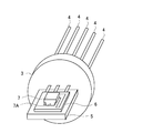
- FIG. 7 is a perspective view for explaining the assembling operation of the semiconductor laser device.
- reference numeral 3 denotes a first base called a stem constituting the semiconductor laser device, and the lead terminal 4 is fixed and the base 5 (second base) is fixed.
- 6 is a sub-base which is fixed to the base 5 and on which a pattern electrically connected to the lead terminal 4 is formed, and a laser chip 7 for generating and emitting a laser beam is fixed by soldering Are configured to
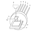
- FIG. 8 shows where the laser chip 7 is fixed on the sub base 6 by soldering, and the alignment during such fixing operation will be described.
- reference numeral 8 denotes an imaging device
- the assembling operator aligns the laser chip 7 with the imaging device 8 while looking at a screen of a monitor taken from the upper surface of the laser chip 7.
- the position of the laser chip 7 is adjusted while looking at the monitor screen so that the corner portion of the laser chip 7 matches the reference position of the pattern provided on the sub base 6. And when the position matches, it is fixed by soldering.
- the laser chip 7 is formed by laminating a plurality of semiconductor layers on the semiconductor substrate, since the laser chip 7 is laminated with a certain degree of inclination, even if the recognition mark is provided on the upper surface of the laser chip 7 Due to the error, the relative position between the recognition mark and the light emitting point 7A is shifted. Therefore, it was difficult to accurately recognize the position of the light emitting point 7A using the recognition mark provided on the upper surface.
- the present invention is intended to provide a semiconductor laser device capable of solving such problems, a method of manufacturing the same, and an optical pickup device.
- a semiconductor laser device includes a fixed portion and a laser chip fixed to the fixed portion, and a recognition mark that can be recognized is provided on an end face of the laser chip from which laser light is emitted. I assume.
- the optical pickup device of the present invention is characterized by including the semiconductor laser device having such a configuration.
- a step of preparing a laser chip provided with a recognizable recognition mark on an end face where laser light is emitted, and recognition of the recognition mark by an imaging device thus, the laser chip and the fixing portion are aligned, and the laser chip is fixed to the fixing portion.
- the recognition mark is provided on the end face where the light emitting point to which the laser beam of the laser chip is emitted is provided. Therefore, since the light emitting point and the recognition mark are provided on the same surface, the position of the light emitting point can be accurately recognized from the recognition mark, and as a result, the laser chip is fixed at the correct position on the sub base. You can do it.
- the optical axis of the laser light emitted from each laser element is specified. It can be set to the position of.
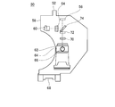
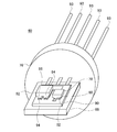
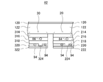
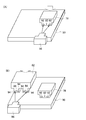
- FIG. 1 It is a perspective view which shows the laser chip integrated in the semiconductor laser apparatus of this invention. It is a top view which shows the optical pick-up apparatus of this invention. It is a perspective view showing the semiconductor laser device of the present invention. It is sectional drawing which shows the laser chip integrated in the semiconductor laser apparatus of this invention in detail. It is sectional drawing which shows the laser chip integrated in the semiconductor laser apparatus of this invention in detail. (A) and (B) are perspective views which show the manufacturing method of the semiconductor laser apparatus of this invention. It is a perspective view which shows the semiconductor laser apparatus applicable to this invention. It is a perspective view for demonstrating the assembly operation of the semiconductor laser apparatus applicable to this invention. It is a figure for demonstrating the arrangement
- the present invention forms alignment marks on the side surface of a laser chip, and takes up a pickup as an application example.
- the present invention is applied to a light emitting chip or a laser chip that requires highly accurate alignment.
- FIG. 1 is a perspective view for explaining a laser chip according to the present invention.
- the recognition mark is provided in a region that does not affect the laser light generation operation.
- a pair of positioning marks 9A and 9B are formed on both sides of the light emitting point 7A.
- a virtual line passing the light emitting point is drawn, and it is assumed that the point intersects the layer on which the mark is formed, and the mark is sandwiched with respect to this point taking it.
- the layer in which the mark is formed is, for example, a block layer and a layer of the n-side electrode 100.
- an optimum material is formed as a mark by using a normal semiconductor process technology.
- the distance between the light emitting point 7A and the marks 9A and 9B can be set accurately.
- the end face of the laser chip 7 is removed by the imaging device 8 and position recognition of the marks 9A and 9B is performed.
- the positional relationship between the marks 9A and 9B and the reference position on the sub base 6 is calculated by the recognition device, and the laser chip 7 is arranged by the manipulator operating in conjunction based on the data of the recognition device. Since the positional relationship between the marks 9A and 9B and the light emitting point 7A of the laser chip 7 is accurately formed by the semiconductor process as described above, the laser chip 7 can be accurately arranged at the set position on the sub base 6 . In particular, if the paste such as Ag or the like is heated and cooled while being fixed by this manipulator or another fixing means, the position of the light emitting point 7A is also fixed at the best position.
- a pair of positioning marks is provided, but the number is not limited and may be, for example, one.
- an optical pickup device 50 provided with the laser semiconductor device of the present embodiment will be described.
- the optical pickup device 50 focuses laser light of BD (Blu-ray Disc), DVD (Digital Versatile Disk) or CD (Compact Disk) standard on the information recording layer of the optical disc (information recording medium), and this information recording is performed. It has a function of receiving the reflected light from the layer and converting it into an electrical signal. It also has a function of writing information on the optical disc.
- the optical pickup device 50 does not necessarily have to correspond to laser beams of three types of standards, and may correspond to laser beams of one or two standards. In other words, even if only one laser chip for BD is mounted, only one laser chip like CD / DVD is mounted, or even only one laser chip like BD, CD and DVD is mounted. good.
- the optical pickup device 50 includes a housing 58 and various optical elements incorporated in the housing 58.
- the optical device mainly includes a laser device 60, a diffraction grating 54, a half mirror 74, a 1 ⁇ 4 wavelength plate 72, a collimator lens 70, a raising mirror, an objective lens 64, and a light detector 56 in a housing. Further, an engaging portion 52 with which the guide shaft is engaged is provided at the upper end of the housing 58, and an insertion portion 68 through which the guide shaft is inserted is provided at the lower end.
- the objective lens 64 is fixed to the upper surface of the lens holder 66, and the lens holder 66 is held by the objective lens driving device 62 in a movable state via a wire.
- the laser device 60 includes a laser diode, and the laser beam of the above-described standard is emitted from the laser diode.
- Laser light in the infrared wavelength band 765 nm to 805 nm (eg, 780 nm wavelength) suitable for CD is emitted from the laser diode.
- the laser light emitted from the laser device 60 is separated into 0th-order light, + 1st-order light and -1st-order light by the diffraction grating 54 and reflected by the half mirror 74, and then the quarter-wave plate 72 and the collimator lens 70. And is reflected by a raising mirror (not shown) and focused on the information recording layer of the optical disc by the objective lens 64. Then, the laser beam of the return light reflected by the information recording layer of the optical disk passes through the rising mirror, the collimator lens 70, the 1 ⁇ 4 wavelength plate 72, and the half mirror 74, and then is detected by the photodetector 56 (PDIC) Be done. A control signal is supplied to the coil of the lens holder 66 based on the signal detected by the light detector 56. As a result, focus control and the like are performed.
- the laser device 60 incorporated in the optical pickup device will be described with reference to FIG.
- the configuration of the laser device 60 shown in this figure is basically the same as that shown in FIG. However, the difference is that two laser chips are fixed to the sub base 90.
- the laser device 60 includes a disc-shaped stem 76 (first base), a base 88 (second base) fixed to the stem 76, and a sub-base fixed to the upper surface of the base 88. 90, a laser chip 78 fixed on the upper surface of the sub base 90, and a plurality of lead terminals 93 penetrating the stem 76 and leading to the outside, the laser chip and the lead terminals are electrically It is connected.
- the laser chip 78 is a chip that emits laser light of the BD standard, and a light emitting point 80 is provided on the side surface (end surface) on the front side in the drawing, and a recognition mark 92 is provided close to the light emitting point 80. It is done.
- the recognition mark 92 is provided to position the laser chip 78 at a predetermined position, the details of which will be described in detail with reference to FIG.
- the laser chip 78 of the BD standard is smaller than the laser chip 82 of the CD / DVD standard described later.
- the laser chip 82 is a chip that emits laser light of the CD standard and the DVD standard, and two light emitting points 84 and 86 are provided on the front side in the drawing.
- laser light of the CD standard (or DVD standard) is emitted from the light emitting point 86
- laser light of the DVD standard (or CD standard) is emitted from the light emitting point 84.
- the recognition mark 94 is provided on the end face where the light emitting points 84 and 66 are provided. Then, using this recognition mark 94, the laser chip 82 is fixed to the sub base 90 with high accuracy.
- various means can be adopted as means for connecting the electrodes provided on the upper and lower surfaces of the laser chips 78 and 82 and the lead terminal 93.
- the upper surface electrodes of the laser chips 78 and 82 are connected to the lead terminals 93 via, for example, connection means such as thin metal wires and a conductive pattern formed on the upper surface of the sub base 90.
- connection means such as thin metal wires and a conductive pattern formed on the upper surface of the sub base 90.
- the electrodes provided on the lower surfaces of the laser chips 78 and 82 are electrically connected to the lead terminals 93, for example, via the conductive patterns formed on the upper surface of the sub base 90.
- the configuration of the laser chip 78 that emits laser light of the BD standard will be described with reference to FIG.
- the laser chip 78 is a blue-violet semiconductor laser device formed of a semiconductor layer of a nitride compound.
- the laser chip 78 includes an n-type cladding layer 104 of n-type AlGaN, a quantum well layer of InGaN having a high In composition, and an In composition on the main surface (the lower surface in the drawing) of the n-type GaN substrate 102.
- MQW multiple quantum well
- the p-type cladding layer 108 has a convex portion and flat portions extending on both sides of the convex portion.
- a ridge portion 114 for forming an optical waveguide is formed in a portion of the active layer 106 by the convex portion of the p-type cladding layer 108.
- a light emitting point 80 for emitting laser light is formed at the end of the active layer 106 above the ridge portion 114.
- a current blocking layer 110 made of an insulating film (for example, SiO 2 or SiN) is formed to cover the lower surface of the flat portion of the p-type cladding layer 108 and the side surface of the ridge portion 114.
- the p-type cladding layer 108 and the current blocking layer 110 are formed.
- a p-side electrode 112 made of Au or the like is formed to cover the lower surface of the p-side electrode.
- an n-side electrode 100 made of Ti, Pt, Au or the like is formed on the upper surface of the n-type GaN substrate 102.
- the recognition mark 92 is exposed from the end face of the current blocking layer 110 made of an insulator.
- the material of the recognition mark 92 is different from the material of the current blocking layer 110 in the light reflectance, and a material which enables the recognition of the recognition mark 92 is adopted.
- a metal material, a semiconductor material or an insulating material is adopted.
- the metal material is mainly made of Al, Au, Pt, Cu, Cr, Ti or the like, and a material having high reflection performance to light can be adopted, and as the semiconductor material, Si etc. It is possible to adopt.
- the insulating material for example, a black resin can be adopted. Since the end face of the laser chip 78 is relatively flat, it is possible to accurately recognize the recognition mark 92 visually.
- the material of the identification mark is coated thereon. Then, patterning is performed so as to straddle lines in a position located on the end face of the chip, and a second block layer is further formed thereon. As a result, when the chip is separated, the line is also cut together and the recognition mark is embedded therein. When the lines are stacked in such a manner as to sandwich the lines, the line dividing property is improved.
- the upper second block layer may not be deposited.
- the end face of the recognition mark is formed so as to appear immediately before the end face, it is not flush with the end face, but it can be adopted as a recognition mark.
- the black resin described above is suitable because it is vulnerable to heat.
- the recognition mark 92 can also be provided on the n-side electrode 100 that covers the top surface of the GaN substrate 102.
- most of the end face of the n-side electrode 100 may be made of Au (gold) and a portion thereof may be made of W (tungsten), so that the portion made of W (tungsten) can be used as a recognition mark. is there.
- a part of the resin film that covers the upper surface of the n-side electrode 100 may be used as a recognition mark.
- the recognition mark 92 is formed together with the current block layer 110 by a semiconductor process, in particular, a lithography technique, so that the recognition mark 92 can be arranged with high accuracy, for example, within ⁇ 1 ⁇ m. Furthermore, in the thickness direction, the recognition mark 92 is disposed in the immediate vicinity of the light emitting point 80. That is, it can be made in the laser chip and can be confirmed from the end face.
- the distance L1 between the light emitting point 80 and the recognition mark 92 is, for example, 5 ⁇ m or more and 10 ⁇ m or less, which is very short. Therefore, even if the active layer 106, the p-type cladding layer 108, etc. are stacked in an inclined manner, the distance between the recognition mark 92 and the light emitting point 80 does not greatly shift due to this, so the position of the recognition mark 92 is recognized By doing this, the position of the light emitting point 80 can be accurately recognized.
- the current blocking layer 110 and the recognition mark 92 are made of materials having different light reflectances.
- the material of the current blocking layer 110 is made of SiO 2 or SiN.
- the recognition mark 92 is made of a metal such as Al, Au, Pt, Cu, Cr or Ti. Therefore, since the recognition mark 92 has a light reflectance higher than that of the current block layer 110, the boundary between the two is clear, and it is possible to accurately recognize the position (outer periphery) of the recognition mark 92 by the imaging device. Become.
- two recognition marks 92 are provided at positions sandwiching the ridge portion 114.
- the position recognition of the light emitting point 80 can be performed more accurately.
- the laser chip 82 is a monolithic two-wavelength semiconductor laser device in which the red semiconductor laser device 20 (DVD standard) and the infrared semiconductor laser device 30 (CD standard) are integrated on the same n-type GaAs substrate 122.
- the red semiconductor laser element 20 is formed of a semiconductor layer of a compound containing P (phosphorus). That is, an n-type cladding layer 214 of n-type AlGaInP, an active layer 216 in which a quantum well layer of GaInP and a barrier layer of AlGaInP are alternately stacked on the main surface of the n-type GaAs substrate 122; P-type cladding layer 218 made of AlGaInP is formed.
- the p-type cladding layer 218 has a protrusion and flat portions extending on both sides of the protrusion.
- a ridge portion 224 for forming an optical waveguide is formed in the portion of the active layer 216 by the convex portion of the p-type cladding layer 218.
- a light emitting point 84 for emitting a red laser beam is formed at the end of the active layer 216 above the ridge portion 224.
- a current blocking layer 220 made of an insulating film is formed to cover the surface of the flat portion of the p-type cladding layer 218 and the side surface of the ridge portion 224.
- a p-side electrode 222 made of Au or the like is formed to cover the surfaces of the p-type cladding layer 218 and the current blocking layer 220.
- an n-side electrode 120 made of Ti, Pt, Au or the like is formed on the upper surface of the n-type GaAs substrate 122.
- the infrared semiconductor laser device 30 is formed of a semiconductor layer of a compound containing As (arsenic). That is, an n-type cladding layer 314 made of n-type AlGaAs, a quantum well layer made of AlGaAs having a low Al composition, and a barrier layer made of AlGaAs having a high Al composition are alternately stacked on the main surface of the n-type GaAs substrate 122 An active layer 316 and a p-type cladding layer 318 made of p-type AlGaAs are formed.
- the p-type cladding layer 318 has a convex portion and flat portions extending on both sides of the convex portion.
- a ridge portion 324 for forming an optical waveguide is formed in the portion of the active layer 316 by the convex portion of the p-type cladding layer 318.
- a light emitting point 86 for emitting an infrared laser beam is formed at the end of the active layer 316 above the ridge portion 324.
- a current blocking layer 320 made of an insulating film is formed to cover the surface of the flat portion of the p-type cladding layer 318 and the side surface of the ridge portion 324.
- a p-side electrode 322 made of Au or the like is formed to cover the surfaces of the p-type cladding layer 318 and the current blocking layer 320.
- An n-side electrode 120 is provided on the top surface of the n-type GaAs substrate 122.
- the recognition mark 94 is embedded in the current block layer 220 made of an insulator such as SiO 2 , and this recognition mark 94 is on the end face like the light emitting point 84. It is exposed. Specifically, in the red semiconductor laser device 20, two recognition marks 94 are provided in the current block layer 220 so as to sandwich the ridge portion 224.
- the recognition mark 94 is made of a metal material such as Au, a semiconductor material, an insulating material, etc. and provided close to the light emitting point 84. By visually recognizing the position of the recognition mark 94 when fixing to the position, the position of the light emitting point 84 can be accurately recognized.
- the recognition mark 94 embedded in the current block layer 320 is exposed at the end face. Therefore, by recognizing the position of the recognition mark 94, the position of the light emitting point 86 can be accurately recognized.
- the recognition mark 94 is provided for both of the two light emitting points 84 and 86 provided on the laser chip 82, but the recognition mark 94 is provided for only one of the light emitting points 84 and 86. It is good.
- the recognition mark 92 and the like have a rectangular shape, but a polygonal shape such as a triangle or a pentagon may be adopted as this shape, or a circular shape or an elliptical shape may be used. Furthermore, referring to FIG. 4 etc., although a plurality of recognition marks 92 are provided in the current block layer 110, only one recognition mark 92 may be provided only on the left side or the right side of the ridge portion 114. .
- the recognition mark 94 is provided on both the red semiconductor laser device 20 and the infrared semiconductor laser device 30 included in the laser chip 82, but the recognition mark 94 may be provided on only one of them.
- the recognition mark 94 embedded in the current block layer 220.
- the recognition mark 94 may be provided on the n-side electrode 120, or the recognition mark 94 may be provided from a coating resin that covers the n-side electrode 120.
- FIG. 6A shows a process of mounting the laser chip 78 of the BD standard
- FIG. 6B shows a process of mounting the laser chip 82 of the CD • DVD standard.
- the relatively small BD standard laser chip 78 is first mounted on the sub base 90, and then the relatively large DVD / CD standard laser chip 82 is mounted. ing.
- this order of implementation may be reversed if collet interference is not an issue.
- a laser chip 78 of BD standard is mounted on the upper surface of sub base 90.
- a conductive pattern of a predetermined shape is formed on the upper surface of the sub base 90, and a solder paste, a conductive paste or the like is applied in advance to a region where the laser chip 78 is to be mounted.
- the laser chip 78 is adsorbed on the upper surface by a collet (not shown) or the like and moved to the upper side of the sub base 90. Then, the recognition mark 92 formed on the end face of the laser chip 78 where the light emitting point 80 is provided is photographed by the imaging device 96 from the side. As described above, the recognition mark 92 is exposed laterally from the current blocking layer 110 at the end face of the laser chip 78. Furthermore, the light reflectance of the metal recognition mark 92 is larger than the light reflectance of the current blocking layer made of an insulating material such as silicon oxide. Therefore, the outer edge shape of the recognition mark 92 can be accurately recognized by the imaging device 96.
- the recognition mark 92 is formed by photolithography technology, and the relative positional accuracy between the light emitting point 80 and the recognition mark 92 is very high. Therefore, the position of the light emitting point 80 can be accurately calculated from the image information of the recognition mark 92 captured by the imaging device 96.
- the laser chip 78 is moved by the collet so that the reference position of the sub base 90 and the light emitting point 80 have a predetermined positional relationship, and the laser chip 78 is placed on the upper surface of the solder paste applied to the sub base 90.
- the reference position of the sub base 90 a part of the conductive pattern provided on the upper surface of the sub base 90, the outer peripheral edge portion of the sub base 90, or the like can be adopted.
- the position recognition of the light emitting point 80 is performed by photographing the recognition mark 92 exposed on the end surface (side surface) of the laser chip 78 from the side with the imaging device 96. Therefore, position recognition is continuously performed using the imaging device 96 until the mounting of the laser chip 78 is completed, and the laser chip 78 can be mounted at a predetermined position on the sub base 90.
- the laser chip 82 of the DVD / CD standard is placed on the upper surface of the sub base 90.
- the recognition mark 94 exposed on the end face of the laser chip 82 by the imaging device 96 To shoot.
- the positions of the light emitting points 84 and 86 are calculated from the photographed image data, and the laser chip 82 is moved so that these light emitting points become predetermined positions, and the solder paste or the like applied to the sub base 90
- the laser chip 82 is placed on the top surface.
- recognition marks 94 are provided on the laser chip 82, it is not necessary that all four recognition marks 94 be recognized by the imaging device 96. For example, only two recognition marks 94 approaching the light emitting point 84 may be recognized, or only two recognition marks 94 approaching the light emitting point 86 may be recognized. Furthermore, only any one recognition mark 94 may be recognized.
- the reference of the alignment of the laser chip 82 may be the sub base 90 or the laser chip 78 fixed in the previous step.
- the sub base 90 is used as a reference, the light emitting points 84 and 86 of the laser chip 82 are set to the outer peripheral edge portion of the recognition portion formed of the conductive pattern or the like provided on the sub base 90 and the sub base 90. Alignment is performed to be the position.
- the laser chip 78 is a reference, alignment is performed so that the light emitting points 84 and 86 of the laser chip 82 are at predetermined positions with respect to the light emitting point 80 and the like of the laser chip 78.
- the laser chips 78 and 82 are fixed to the sub base 90 by performing reflow for melting the solder paste or heat curing of the conductive paste. , And electrically connected to the conductive pattern on the sub base 90.
- the position of the laser chips 78 or 82 is fixed by transportation means such as collet continuously until the solder or conductive paste solidifies. It is good. As a result, after the laser chips 78 and 82 are mounted, movement of the laser chips 78 and 82 is suppressed while the solder and the conductive paste are solidified, and further improvement of the positional accuracy is expected. Ru.
- connection means such as metal thin wires.
- various means can be adopted as a means for connecting the laser chips 78 and 82 and the lead terminal 93.
- the upper and lower electrodes of the laser chips 78 and 82 may be directly connected to the lead terminal 93 through a conductive fixing material such as solder.
- the laser device 60 shown in FIG. 3 is manufactured. Further, referring to FIG. 2, the optical pickup device 50 is manufactured by housing the laser device 60 in the housing 58 together with other optical elements.
- semiconductor materials and insulating materials can be adopted other than metal materials.
- part of the side surface of the n-side electrode 120 is made of a metal material (for example, W) different from other parts, and the exposed portion made of W is a recognition mark It may be used as Furthermore, part of the insulating material covering the n-side electrode 120 may be used as a recognition mark.
- W metal material
- the present invention is applicable not only to semiconductor laser devices used in optical pickup devices for reading signals recorded on Blu-ray standard optical disks, DVD standard optical disks, and CD standard optical disks, but also to other optical devices. It can be applied.
- Reference Signs List 3 stem 4 lead terminal 6 sub-base 7 laser chip 7A light emitting point 8 imaging device 9A, 9B mark 20 red semiconductor laser device 30 infrared semiconductor laser device 50 optical pickup device 52 engaging portion 54 diffraction grating 56 light detector 58 housing 60 laser device 62 objective lens drive device 64 objective lens 66 lens holder 68 insertion portion 70 collimator lens 72 quarter wavelength plate 74 half mirror 76 stem 78 laser chip 80 light emitting point 82 laser chip 84 light emitting point 86 light emitting point 88 base 90 Sub base 92 recognition mark 93 lead terminal 94 recognition mark 96 imaging device 100 n-side electrode 102 GaN substrate 104 n-type cladding layer 106 Layer 108 p-type cladding layer 110 current blocking layer 112 p-side electrode 114 ridge portion 120 n-side electrode 122 n-type GaAs substrate 214 n-type cladding layer 216 active layer 218 p-type cladding layer 220 current blocking layer 222 p-side electrode 224
Landscapes
- Physics & Mathematics (AREA)
- Optics & Photonics (AREA)
- Condensed Matter Physics & Semiconductors (AREA)
- General Physics & Mathematics (AREA)
- Electromagnetism (AREA)
- Semiconductor Lasers (AREA)
- Optical Head (AREA)
Abstract
レーザー光を生成放射する半導体レーザー装置に組み込まれるレーザーチップのサブ基台に対する位置合わせを正確に行うことが出来る技術を提供する。 ステムに固定されたリード端子と電気的に接続されたパターンが形成されているとともにレーザー光を生成するレーザーチップ7が半田付けされるサブ基台が前記ステムに固定された半導体レーザー装置であり、前記レーザーチップ7のレーザー光が放射される発光点7Aが設けられている端面に位置決め用の印9A、9Bを設ける。
Description
本発明は、精度の高い位置あわせに用いられ、一例として光ディスクに記録されている信号の読み出し動作、光ディスクへの信号の記録動作に用いられる半導体レーザー装置およびその製造方法、光ピックアップ装置に関する。
光ピックアップ装置から照射されるレーザー光を光ディスクの信号記録層に照射することによって信号の読み出し動作や信号の記録動作を行うことが出来る光ディスク装置が普及している。
光ディスク装置としては、CDやDVDと呼ばれる光ディスクを使用するものが一般に普及しているが、最近では記録密度を向上させた光ディスク、即ちBlu-ray規格の光ディスクを使用するものが開発されている。
CD規格の光ディスクに記録されている信号の読み出し動作を行うレーザー光としては、波長が785nmである赤外光が使用され、DVD規格の光ディスクに記録されている信号の読み出し動作行うレーザー光としては、波長が655nmの赤色光が使用されている。
斯かるCD規格及びDVD規格の光ディスクに対して、Blu-ray規格の光ディスクに記録されている信号の読み出し動作を行うレーザー光としては、波長が短いレーザー光、例えば波長が405nmの青紫色光が使用されている。
光ピックアップ装置において、レーザー光を生成する手段としてレーザーダイオード、即ち半導体レーザー装置が一般に採用されている(特許文献1参照)。
CD規格の光ディスク、DVD規格の光ディスク及びBlu-ray規格の光ディスクの全ての光ディスクに記録されている信号の読み出し動作を行うことが出来る光ピックアップ装置が製品化されているが、斯かる光ピックアップ装置には異なる波長のレーザー光を生成放射するレーザーダイオードが組み込まれることになる。
前述した3つの規格の光ディスクに記録されている信号の読み出し動作を行うことが出来る光ピックアップ装置は、CD規格の光ディスク及びDVD規格の光ディスクに対応する2波長のレーザー光を生成する2波長レーザーダイオードとBlu-ray規格の光ディスクに対応する波長のレーザー光を生成するレーザーダイオードの2つのレーザーダイオードが一般に組み込まれている。
斯かる2つのレーザーダイオードが組み込まれた光ピックアップ装置は、光学系の構成が複雑になるため高価になるだけでなく組立作業の工数が多くなるという問題がある。この問題を解決するために最近では、3つの異なる波長のレーザー光を生成するレーザーチップを1つのケース内に設けるように構成された3波長対応のレーザーダイオードが開発されている。
前述した様に、図9は、1つのケース内に2つのレーザーチップが組み込まれたもので、特にチップの配置を示すものである。同図において、1はCD用レーザー素子及びDVD用レーザー素子がモノリシック技術にて製造されている2波長レーザーチップであり、1C及び1DはCD用レーザー素子の発光点及びDVD用レーザー素子の発光点である。
2はBlu-ray用レーザーチップであり、2BはBlu-ray用レーザー素子の発光点である。そして、前記3波長対応のレーザーダイオードでは、前記2波長レーザーチップ1及びBlu-ray用レーザーチップ2が1つのケース内に組み込まれている。
前述した3波長のレーザーダイオードが組み込まれた光ピックアップ装置は、光学系の光路を共用することが出来るので、光学構成を簡潔にすることが出来るという利点を有する。しかし、レーザーダイオードに組み込まれている各レーザー光の発光点は、図9に示すように、3箇所別々の所に配置されるので、各レーザー光の光軸がずれることになる。
2波長レーザーチップ1内に形成されるCD用レーザー素子とDVD用レーザー素子とは、前述したようにモノリシック技術によって製造されるので、CD用レーザー素子の発光点1CとDVD用レーザー素子の発光点1Dとの間の位置関係は精度良く設定されることになる。これに対して、Blu-ray用レーザーチップ2は、別チップであるため、ラテラルのハイブリッド型として、組み込まれるので、DVD用レーザー素子の発光点1DとBlu-ray用レーザー素子の発光点2Bとの間の距離Lにバラツキが発生することになる。
図7は半導体レーザー装置の組立動作を説明するための斜視図である。同図において、3は半導体レーザー装置を構成するステムと呼ばれる第1の基台であり、リード端子4が固定されているとともに基台5(第2の基台)が固定されている。6は前記基台5に固定されているとともに前記リード端子4と電気的に接続されるパターンが形成されているサブ基台であり、レーザー光を生成放射するレーザーチップ7が半田付けによって固定されるように構成されている。
図8は、レーザーチップ7が前記サブ基台6上に半田付けにて固定される所を示すものであり、斯かる固定動作時の位置合わせについて説明する。
図8において、8は撮像装置であり、組立作業者は、この撮像装置8にて、レーザーチップ7の上面から撮影されるモニターの画面を見ながら、レーザーチップ7の位置合わせを行う。例えばレーザーチップ7のコーナー部が、サブ基台6上に設けられているパターンの基準位置に合致するように、モニター画面を見ながらレーザーチップ7の位置を調整する。そしてその位置が合致した時、半田付けによって、固定される。
斯かる従来の固定方法では、レーザーチップ7の外形や電極等を基準にして位置合わせをするので、形状や電極に寸法誤差があったり、変形があったりすると、発光点7Aが最良の位置からずれるという問題がある。
また、レーザーチップ7は、半導体基板に複数層の半導体層を積層して形成されるが、ある程度の傾斜をもって積層されるため、レーザーチップ7の上面に認識マークを設けたとしても、製造時の誤差により、この認識マークと発光点7Aとの相対的位置がずれてしまう。よって、この上面に設けた認識マークを使用して発光点7Aの位置を正確に認識することは困難であった。
また、レーザーチップ7の位置を認識する方法として、レーザーチップ7からレーザー光を放射させ、このレーザー光を受光し、レーザー光の位置から、チップの位置調整をすることも考えられる。しかしながら、この方法では、レーザーチップを発光させつつ位置合わせを行う必要があり、位置合わせ工程が複雑となりコストアップを招いていた。
本発明は、斯かる問題を解決することが出来る半導体レーザー装置およびその製造方法、光ピックアップ装置を提供しようとするものである。
本発明の半導体レーザー装置は、固定部と、前記固定部に固着されたレーザーチップとを備え、前記レーザーチップのレーザー光が放射される端面に、認識可能な認識マークが設けられたことを特徴とする。
更に、本発明の光ピックアップ装置は、かかる構成の半導体レーザー装置を備えたことを特徴とする。
更に、本発明の半導体レーザー装置の製造方法は、レーザー光が放射される端面に、認識可能な認識マークが設けられたレーザーチップを用意する工程と、撮像装置にて、前記認識マークを認識することにより、前記レーザーチップと固定部とを位置合わせして、前記レーザーチップを前記固定部に固着することを特徴とする。
本発明の半導体レーザー装置では、レーザーチップのレーザー光が放射される発光点が設けられている端面に認識マークを設けた。よって、発光点と認識マークとが同一の面に設けられているので、発光点の位置を認識マークから正確に認識することが出来、その結果レーザーチップをサブ基台上の正確な位置に固定することが出来る。
更に本発明によれば、3つの波長が異なるレーザー光を生成放射するレーザー素子が同一のケース内に組み込まれる半導体レーザー装置に実施した場合、各レーザー素子から放射されるレーザー光の光軸を所定の位置に設定することが出来る。
本発明は、レーザーチップの側面に合わせマークを形成するもので、応用例としてピックアップを取り上げている。しかしながら、精度の高い位置あわせが必要となる発光チップ、またはレーザーチップに適用されるものである。
<第1の実施の形態>
<第1の実施の形態>
本形態では、本願発明の基本的な構成を説明する。本構成は、図3の様に、レーザーチップをステム76上のサブ基台90に固定する場合、その位置合わせを正確に行うことが出来るものである。
図1は本発明に係るレーザーチップを説明するための斜視図である。
本発明は、レーザーチップ7の発光点7Aが設けられている端面に於いて、レーザー光の生成動作に影響を与えない領域に、認識マークを設けるものである。ここでは、端面に於いて、前記発光点7Aを中心にして、この両側を挟んで一対の位置決め用の印9A及び9Bが作りこまれている。
具体的には、図1の端面で説明すれば、発光点を通過する仮想的な線を引き、印が形成される層と交差する点を想定し、この点に対して印が挟む形を取っている。印が形成される層は、例えばブロック層であり、またn側電極100の層である。尚、ここでは、通常の半導体プロセス技術を使い、マークとして最適な材料が形成される。
半導体プロセスは、一般にフォトリソグラフィ技術を使うため、その位置精度は高い。よって、発光点7Aと印9A及び9Bとの距離を正確に設定出来る。斯かる構成のレーザーチップ7をサブ基台6に固定する場合、撮像装置8にてレーザーチップ7の端面をのぞき、印9A及び9Bを位置認識することによって行われる。
即ち、印9A及び9Bとサブ基台6上の基準位置との位置関係が、認識装置により演算され、この認識装置のデータに基づいて連動するマニュピレータにより、レーザーチップ7が配置される。印9A及び9Bとレーザーチップ7の発光点7Aとの位置関係は、前述した様に半導体プロセスで作りこまれて正確なため、レーザーチップ7をサブ基台6上の設定位置に精度高く配置できる。特にこのマニュピレータ、または別の固定手段にて固定しつつ、半田付け、またはAg等のペーストを加温冷却すれば、発光点7Aの位置も最良の位置に固定される。
尚、本実施例では、位置決め用の印を一対設けたが、その数は限定されるものではなく、例えば1つであっても良い。
<第2の実施の形態>
<第2の実施の形態>
本形態では、第1の実施の形態を具体的に説明する。
先ず、図2を参照して、本形態のレーザ半導体装置を備えた光ピックアップ装置50を説明する。
光ピックアップ装置50は、BD(Blu-ray Disc)、DVD(Digital Versatile Disk)またはCD(Compact Disk)規格のレーザー光を、光ディスク(情報記録媒体)の情報記録層に合焦させ、この情報記録層からの反射光を受光して電気信号に変換する機能を備えている。また前記光ディスクに情報を書き込む機能を有している。ここで、光ピックアップ装置50は、必ずしも3種類の規格のレーザー光に対応する必要はなく、1つまたは2つの規格のレーザー光に対応しても良い。つまりBD用のレーザーチップが1つだけ載せられたり、CD/DVD様のレーザーチップが1つだけが載せられたり、更には、BD、CDおよびDVD様のレーザーチップが一つだけ載せられても良い。
光ピックアップ装置50は、ハウジング58と、このハウジング58に内蔵された各種光学素子を備えている。光学素子は、主に、レーザー装置60、回折格子54、ハーフミラー74、1/4波長板72、コリメータレンズ70、立ち上げミラー、対物レンズ64および光検出器56がハウジングに内蔵される。また、ハウジング58の上端には、ガイド軸が係合される係合部52が設けられ、下端には、ガイド軸が挿通される挿通部68が設けられている。
対物レンズ64はレンズホルダ66の上面に固着されており、このレンズホルダ66はワイヤを介して移動可能な状態で対物レンズ駆動装置62に保持されている。
レーザー装置60はレーザーダイオードを備え、このレーザーダイオードから上記した規格のレーザー光が放射される。具体的には、BDに適した青紫色(青色)波長帯395nm~420nm(例えば405nmの波長)のレーザー光、DVDに適した赤色波長帯645nm~675nm(例えば650nmの波長)のレーザー光、またはCDに適した赤外波長帯765nm~805nm(例えば780nmの波長)のレーザー光が、レーザーダイオードから放射される。
レーザー装置60から放射されたレーザー光は、回折格子54で0次光、+1次光、-1次光に分離されてハーフミラー74で反射された後に、1/4波長板72およびコリメータレンズ70を通過し、不図示の立ち上げミラーで反射されて対物レンズ64で光ディスクの情報記録層に合焦される。そして、光ディスクの情報記録層で反射した戻り光のレーザー光は、立ち上げミラー、コリメータレンズ70、1/4波長板72、ハーフミラー74を透過し、その後、光検出器56(PDIC)で検出される。光検出器56で検出された信号に基づいて、レンズホルダ66のコイルに制御信号が供給される。この結果、フォーカス制御等が行われる。
図3を参照して、光ピックアップ装置に組み込まれるレーザー装置60を説明する。この図に示すレーザー装置60の構成は、図7に示したものと基本的には同様である。ただ、2つのレーザーチップがサブ基台90に固着されている点で異なる。
レーザー装置60は、円盤形のステム76(第1の基台)と、ステム76に固定された基台88(第2の基台)と、この基台88の上面に固着されたサブ基台90と、サブ基台90の上面に固着されたレーザーチップ78、82と、ステム76を貫通し、外部に導出する複数のリード端子93を有し、前記レーザーチップと前記リード端子は電気的に接続されている。
レーザーチップ78は、BD規格のレーザー光を放射するチップであり、紙面上で手前の側面(端面)に発光点80が備えられており、更に、発光点80に接近して認識マーク92が設けられている。この認識マーク92は、レーザーチップ78を所定の位置に配置するために設けられ、この詳細は図4を参照して詳述する。BD規格のレーザーチップ78は、後述するCD・DVD規格のレーザーチップ82よりも小型に形成されている。
レーザーチップ82は、CD規格およびDVD規格のレーザー光を放射するチップであり、紙面上にて手前側に、2つの発光点84、86が設けられている。ここでは、発光点86からCD規格(またはDVD規格)のレーザー光が放射され、発光点84からDVD規格(またはCD規格)のレーザー光が発光される。前述したレーザーチップ78と同様に、レーザーチップ82においても、発光点84、66が設けられる端面に、認識マーク94が設けられる。そして、この認識マーク94を用いて、レーザーチップ82は、サブ基台90に精度高く固定される。
また、レーザーチップ78、82の上面および下面に設けられた電極とリード端子93とを接続する手段としては様々なものが採用可能である。レーザーチップ78、82の上面電極は、例えば、金属細線等の接続手段、およびサブ基台90の上面に形成された導電パターンを経由してリード端子93と接続される。一方、レーザーチップ78、82の下面に設けられた電極は、例えば、サブ基台90の上面に形成された導電パターンを介して、リード端子93と導通している。
図4を参照して、BD規格のレーザー光を放射するレーザーチップ78の構成を説明する。
レーザーチップ78は、窒化物系化合物の半導体層により形成された青紫色半導体レーザー素子である。具体的には、レーザーチップ78は、n型GaN基板102の主面上(紙面では下面)に、n型AlGaNからなるn型クラッド層104、In組成の高いInGaNからなる量子井戸層とIn組成の低いInGaNからなる障壁層とが交互に積層された多重量子井戸(MQW)構造を有する活性層106、および、p型AlGaNからなるp型クラッド層108が形成されている。
また、p型クラッド層108は、凸部と、凸部の両側に延びる平坦部とを有している。このp型クラッド層108の凸部によって、活性層106の部分に光導波路を構成するためのリッジ部114が形成されている。これによりリッジ部114上方の活性層106の端部に、レーザー光を出射する発光点80が形成される。
p型クラッド層108の平坦部の下面とリッジ部114の側面とを覆うように絶縁膜(例えばSiO2やSiN)からなる電流ブロック層110が形成され、p型クラッド層108および電流ブロック層110の下面を覆うように、Auなどからなるp側電極112が形成されている。
また、n型GaN基板102の上面に、Ti、Pt、Au等からなるn側電極100が形成されている。
本形態では、絶縁物から成る電流ブロック層110の端面から、認識マーク92を露出させている。
認識マーク92の材料としては、電流ブロック層110の材料と光の反射率が異なり、認識マーク92の認識を可能とする材料が採用され、例えば金属材料、半導体材料または絶縁材料が採用される。ここで、金属材料としてはAl、Au、Pt、Cu、CrまたはTi等を主材料としたもので、光に対して高反射性能を有する材料が採用可能であり、半導体材料としてはSi等が採用可能である。また、絶縁材料としては、例えば黒色系の樹脂が採用できる。レーザーチップ78の端面は、比較的フラットであるため、認識マーク92を正確に視覚的に認識することが可能である。
例えば、ウェハ状態で第1のブロック層を途中まで成膜したら、その上に、認識マークの材料を被覆する。そしてチップの端面に位置する所を、ライン状に跨ぐ様に、パターニングし、更にその上に第2のブロック層を成膜する。これにより、チップとして分離する際、一緒にラインも分断され、そこに認識マークが盛り込まれることになる。このようにラインを挟み込むように積層すれば、ラインの分断性が良くなる。
また上層の第2のブロック層を成膜しなくても良い。この場合、端面のごく手前で認識マークの端面が現れるように形成すれば、端面と面一にはならないが、認識マークとして採用できる。前述した黒色の樹脂は、熱に弱いことから好適である。
更に、認識マーク92は、GaN基板102の上面を被覆するn側電極100に設けることも可能である。例えば、n側電極100の端面の大部分をAu(金)から構成し、一部をW(タングステン)から構成することで、このW(タングステン)から成る部分を認識マークとすることも可能である。また、n側電極100の上面を被覆する樹脂膜の一部を認識マークとして用いても良い。
認識マーク92は、電流ブロック層110と共に半導体プロセス、特にリソグラフィー技術により形成されるため、例えば±1μm以内の誤差で高精度に配置させることできる。更に、厚み方向に於いて、認識マーク92は発光点80の直近に配置される。つまりレーザーチップの中に作りこまれ、端面から確認することができる。
発光点80と認識マーク92との距離L1は、例えば5μm以上10μm以下であり非常に短い。よって、活性層106、p型クラッド層108等が傾斜して積層されたとしても、このことにより認識マーク92と発光点80との距離が大きくズレることは無いので、認識マーク92の位置を認識することにより、発光点80の位置を正確に認識することが可能となる。
更に、電流ブロック層110と認識マーク92とは、光の反射率が異なる材料から成る。上記したように、電流ブロック層110の材料はSiO2やSiNから成る。一方、認識マーク92は、Al、Au、Pt、Cu、CrまたはTi等の金属等から成る。よって、認識マーク92が電流ブロック層110よりも光の反射率が大きいので、両者の境界は明瞭であり、撮像装置により認識マーク92の位置(外周縁部)を正確に認識することが可能となる。
更に本形態では、リッジ部114を挟む位置に2つの認識マーク92を設けている。これにより、撮像装置で2つの認識マーク92を認識することで、より正確に発光点80の位置認識を行うことができる。
図5の断面図を参照して、レーザーチップ82の具体的構成について説明する。
レーザーチップ82は、同一のn型GaAs基板122に赤色半導体レーザー素子20(DVD規格)と赤外半導体レーザー素子30(CD規格)を集積化したモノリシック2波長半導体レーザー素子である。
赤色半導体レーザー素子20は、P(リン)を含む化合物の半導体層により形成されている。すなわち、n型GaAs基板122の主面上に、n型AlGaInPからなるn型クラッド層214、GaInPからなる量子井戸層とAlGaInPからなる障壁層とが交互に積層された活性層216、および、p型AlGaInPからなるp型クラッド層218が形成されている。
p型クラッド層218は、凸部と、凸部の両側に延びる平坦部とを有している。このp型クラッド層218の凸部によって、活性層216の部分に光導波路を構成するためのリッジ部224が形成されている。これによりリッジ部224上方の活性層216の端部に、赤色のレーザー光を出射する発光点84が形成される。
p型クラッド層218の平坦部の表面とリッジ部224の側面とを覆うように絶縁膜からなる電流ブロック層220が形成されている。p型クラッド層218および電流ブロック層220の表面を覆うように、Auなどからなるp側電極222が形成されている。また、n型GaAs基板122の上面に、Ti、Pt、Au等からなるn側電極120が形成されている。
赤外半導体レーザー素子30は、As(ヒ素)を含む化合物の半導体層により形成されている。すなわち、n型GaAs基板122の主面に、n型AlGaAsからなるn型クラッド層314、Al組成の低いAlGaAsからなる量子井戸層とAl組成の高いAlGaAsからなる障壁層とが交互に積層された活性層316、および、p型AlGaAsからなるp型クラッド層318が形成されている。
p型クラッド層318は、凸部と、凸部の両側に延びる平坦部とを有している。このp型クラッド層318の凸部によって、活性層316の部分に光導波路を構成するためのリッジ部324が形成されている。これによりリッジ部324上方の活性層316の端部に、赤外のレーザー光を出射する発光点86が形成される。
p型クラッド層318の平坦部の表面とリッジ部324の側面とを覆うように絶縁膜からなる電流ブロック層320が形成されている。p型クラッド層318および電流ブロック層320の表面を覆うように、Auなどからなるp側電極322が形成されている。n型GaAs基板122の上面はn側電極120が設けられる。
この図に示すレーザーチップ82の赤色半導体レーザー素子20でも、SiO2等の絶縁物から成る電流ブロック層220に認識マーク94が埋め込まれており、この認識マーク94が発光点84と同様に端面に露出している。具体的には、赤色半導体レーザー素子20では、リッジ部224を挟むように、電流ブロック層220に2つの認識マーク94が設けられている。
認識マーク94は、図4に示した認識マーク92と同様に、Au等の金属材料、半導体材料、絶縁材料等から成り、発光点84の直近に設けられているので、レーザーチップ82を所定位置に固着する際に、認識マーク94の位置を視覚的に認識することで、発光点84の位置を正確に位置認識できる。
赤外半導体レーザー素子30に於いても、同様に、電流ブロック層320に埋め込まれた認識マーク94が端面に露出している。これにより、認識マーク94の位置を認識することにより、発光点86の位置を正確に認識できる。
ここで、上記では、レーザーチップ82に設けられる2つの発光点84、86の両方に対して認識マーク94を設けたが、発光点84、86の何れか一方のみに対して認識マーク94を設けても良い。
また、図4を参照して、認識マーク92等は四角形形状を呈しているが、この形状は、三角形や五角形等の多角形形状が採用されても良いし、円形状や楕円形状でも良い。更に、図4等を参照すると、電流ブロック層110に複数の認識マーク92が設けられているが、リッジ部114の左方または右方のみに1つのみの認識マーク92が設けられても良い。
更に、図5では、レーザーチップ82に含まれる赤色半導体レーザー素子20および赤外半導体レーザー素子30の両方に認識マーク94を設けたが、何方か一方のみに認識マーク94を設けても良い。
ここでも、図4に示したレーザーチップ78と同様に、電流ブロック層220に埋め込まれる認識マーク94としては、種々の材料が採用可能である。また、上記と同様に、n側電極120に認識マーク94が設けられても良いし、n側電極120を被覆する被覆樹脂から認識マーク94が設けられても良い。
<第3の実施の形態>
<第3の実施の形態>
本形態では、図6を参照して、上記したレーザーチップをサブ基台に実装する工程を説明する。図6(A)はBD規格のレーザーチップ78を実装する工程を示し、図6(B)はCD・DVD規格のレーザーチップ82を実装する工程を示す。
ここでは、チップを輸送するコレットの干渉を防ぐために、比較的小型なBD規格のレーザーチップ78を先ずサブ基台90に実装した後に、比較的大型なDVD・CD規格のレーザーチップ82を実装している。しかしながら、コレットの干渉が問題にならなければ、この実装の順番は逆でも良い。
図6(A)を参照して、先ず、BD規格のレーザーチップ78をサブ基台90の上面に実装する。ここで、サブ基台90の上面には所定形状の導電パターンが形成されており、レーザーチップ78が実装予定の領域には半田ペーストや導電ペースト等が予め塗布されている。
レーザーチップ78は、不図示のコレット等で上面を吸着されてサブ基台90の上方に移動される。そして、発光点80が設けられるレーザーチップ78の端面に形成された認識マーク92を、側方から撮像装置96で撮影する。上記したように、認識マーク92は、レーザーチップ78の端面にて、電流ブロック層110から側方に露出している。更に、金属から成る認識マーク92の光の反射率は、酸化シリコン等の絶縁材料から成る電流ブロック層の光の反射率よりも大きい。よって、認識マーク92の外縁形状は、撮像装置96で正確に認識することが可能である。
更に、上記したように、認識マーク92はフォトリソグラフィー技術で形成されており、発光点80と認識マーク92との相対的な位置精度は非常に高い。よって、撮像装置96で撮影された認識マーク92の画像情報から、発光点80の位置を正確に算出できる。
その後、サブ基台90の基準位置と発光点80とが所定の位置関係となるように、コレットでレーザーチップ78を移動させて、サブ基台90に塗布された半田ペーストの上面に載置する。ここで、サブ基台90の基準位置としては、サブ基台90の上面に設けられた導電パターンの一部やサブ基台90の外周縁部等が採用可能である。
本工程では、レーザーチップ78の端面(側面)に露出する認識マーク92を側方から撮像装置96で撮影することで、発光点80の位置認識を行なっている。従って、レーザーチップ78の載置が終了するまで連続して撮像装置96を用いて位置認識を行い、レーザーチップ78をサブ基台90上の所定位置に載置することが可能となる。
図6(B)を参照して、次に、DVD・CD規格のレーザーチップ82をサブ基台90の上面に載置する。具体的には、上記と同様に、コレット等の輸送手段を用いてレーザーチップ82をサブ基台90の上方に移動させた後に、撮像装置96で、レーザーチップ82の端面に露出する認識マーク94を撮影する。そして、撮影された画像データから発光点84、86の位置を算出し、これらの発光点が所定位置となるようにレーザーチップ82を移動させて、サブ基台90に塗布された半田ペースト等の上面にレーザーチップ82を載置する。
ここで、レーザーチップ82には合計で4つの認識マーク94が設けられているが、必ずしも4つ全ての認識マーク94が撮像装置96で認識される必要はない。例えば、発光点84に接近する2つの認識マーク94のみが認識されても良いし、発光点86に接近する2つの認識マーク94のみが認識されても良い。更には、何れか1つのみの認識マーク94のみが認識されても良い。
また、レーザーチップ82の位置合わせの基準は、サブ基台90でも良いし、先工程で固着されたレーザーチップ78でも良い。サブ基台90を基準とする場合は、サブ基台90に設けられた導電パターン等から成る認識部やサブ基台90の外周縁部に対して、レーザーチップ82の発光点84、86が所定位置となるように位置合わせが行われる。一方、レーザーチップ78が基準となる場合は、レーザーチップ78の発光点80等に対して、レーザーチップ82の発光点84、86が所定位置と成るように位置合わせが行われる。
上記工程にて、レーザーチップ78、82の載置が終了した後は、半田ペーストを溶融するリフローや、導電ペーストの加熱硬化を行うことで、レーザーチップ78、82をサブ基台90に固着し、サブ基台90上の導電パターンと電気的に接続する。
ここで、半田や導電ペーストを用いてレーザーチップ78、82を固着する際に、半田や導電ペーストが固化するまで連続して、コレット等の輸送手段等によりレーザーチップ78、82の位置を固定しても良い。これにより、レーザーチップ78、82を載置した後に、半田や導電ペーストが固化するまでの間に、レーザーチップ78、82が移動してしまうことが抑制され、位置精度の更なる向上が期待される。
また、レーザーチップ78、82上面に設けられた電極と、サブ基台90上の導電パターンとを金属細線等の接続手段で接続する。
ここで、図3を参照して、レーザーチップ78、82とリード端子93とを接続する手段としては様々なものが採用可能である。例えば、レーザーチップ78、82の上面電極および下面電極が、半田等の導電固着材を介してリード端子93に直に接続されても良い。
上記工程により、図3に示すレーザー装置60が製造される。また、図2を参照して、このレーザー装置60を他の光学素子と共にハウジング58に収納させることで光ピックアップ装置50が製造される。
ここで、第2の実施の形態で述べたように、認識マーク92の材料としては、金属材料以外にも、半導体材料や絶縁材料が採用可能である。
更に、図5を参照して説明したように、n側電極120の側面の一部を、他の部分とは異なる金属材料(例えばW)で構成し、この露出するWから成る部位を認識マークとして用いても良い。更にまた、n側電極120を被覆する絶縁材料の一部を認識マークとして用いても良い。
本発明は、Blu-ray規格の光ディスク、DVD規格の光ディスク及びCD規格の光ディスクに記録されている信号を読み出すための光ピックアップ装置に使用される半導体レーザー装置だけでなく、その他の光学装置にも応用することが出来る。
3 ステム
4 リード端子
6 サブ基台
7 レーザーチップ
7A 発光点
8 撮像装置
9A,9B 印
20 赤色半導体レーザー素子
30 赤外半導体レーザー素子
50 光ピックアップ装置
52 係合部
54 回折格子
56 光検出器
58 ハウジング
60 レーザー装置
62 対物レンズ駆動装置
64 対物レンズ
66 レンズホルダ
68 挿通部
70 コリメータレンズ
72 1/4波長板
74 ハーフミラー
76 ステム
78 レーザーチップ
80 発光点
82 レーザーチップ
84 発光点
86 発光点
88 基台
90 サブ基台
92 認識マーク
93 リード端子
94 認識マーク
96 撮像装置
100 n側電極
102 GaN基板
104 n型クラッド層
106 活性層
108 p型クラッド層
110 電流ブロック層
112 p側電極
114 リッジ部
120 n側電極
122 n型GaAs基板
214 n型クラッド層
216 活性層
218 p型クラッド層
220 電流ブロック層
222 p側電極
224 リッジ部
314 n型クラッド層
316 活性層
318 p型クラッド層
320 電流ブロック層
322 p側電極
324 リッジ部
Claims (10)
- 固定部と、前記固定部に固着されたレーザーチップとを備え、
前記レーザーチップのレーザー光が放射される端面に、認識可能な認識マークが設けられたことを特徴とする半導体レーザー装置。 - 前記認識マークは、半導体基板を被覆する絶縁材料から成る絶縁層から前記端面に露出する、前記絶縁材料とは光の反射率が異なる材料から成ることを特徴とする請求項1に記載の半導体レーザー装置。
- 前記絶縁層は、SiO2から成る電流ブロック層であることを特徴とする請求項2に記載の半導体レーザー装置。
- 前記認識マークは、金属、半導体材料または絶縁材料から成ることを特徴とする請求項1から請求項3の何れかに記載の半導体レーザー装置。
- 前記認識マークを、前記レーザー光の発光点を挟んで、複数設けたことを特徴とする請求項1から請求項4の何れかに記載の半導体レーザー装置。
- 前記認識マークは、フォトリソグラフィ技術にて形成されたことを特徴とする請求項1から請求項5の何れかに記載の半導体レーザー装置。
- レーザーチップは、第1レーザーチップと、前記第1レーザーチップとは波長が異なるレーザー光を放射する第2レーザーチップとを備え、
前記第1レーザーチップおよび前記第2レーザーチップの両方に、前記認識マークが配置されることを特徴とする請求項1から請求項6の何れかに記載の半導体レーザー装置。 - 請求項1から請求項7の何れかに記載された半導体レーザー装置を備えたことを特徴とする光ピックアップ装置。
- レーザー光が放射される端面に、認識可能な認識マークが設けられたレーザーチップを用意する工程と、
撮像装置にて、前記認識マークを認識することにより、前記レーザーチップと固定部とを位置合わせして、前記レーザーチップを前記固定部に固着することを特徴とする半導体レーザー装置の製造方法。 - 前記撮像装置で側方から前記レーザーチップに設けられた前記認識マークを認識することを特徴とする請求項9に記載の半導体レーザー装置の製造方法。
Applications Claiming Priority (2)
| Application Number | Priority Date | Filing Date | Title |
|---|---|---|---|
| JP2011130792A JP2014157847A (ja) | 2011-06-13 | 2011-06-13 | 半導体レーザー装置 |
| JP2011-130792 | 2011-06-13 |
Publications (1)
| Publication Number | Publication Date |
|---|---|
| WO2012172777A1 true WO2012172777A1 (ja) | 2012-12-20 |
Family
ID=47356784
Family Applications (1)
| Application Number | Title | Priority Date | Filing Date |
|---|---|---|---|
| PCT/JP2012/003812 Ceased WO2012172777A1 (ja) | 2011-06-13 | 2012-06-12 | 半導体レーザー装置およびその製造方法、光ピックアップ装置 |
Country Status (2)
| Country | Link |
|---|---|
| JP (1) | JP2014157847A (ja) |
| WO (1) | WO2012172777A1 (ja) |
Cited By (1)
| Publication number | Priority date | Publication date | Assignee | Title |
|---|---|---|---|---|
| CN116231438A (zh) * | 2022-12-07 | 2023-06-06 | 武汉锐科光纤激光技术股份有限公司 | 一种泵浦源烧结治具及泵浦源芯片的贴合定位方法 |
Families Citing this family (2)
| Publication number | Priority date | Publication date | Assignee | Title |
|---|---|---|---|---|
| US9110685B2 (en) | 2008-03-25 | 2015-08-18 | Qualcomm, Incorporated | Apparatus and methods for managing widgets in a wireless communication environment |
| US9069575B2 (en) | 2008-03-25 | 2015-06-30 | Qualcomm Incorporated | Apparatus and methods for widget-related memory management |
Citations (3)
| Publication number | Priority date | Publication date | Assignee | Title |
|---|---|---|---|---|
| JPH04102810A (ja) * | 1990-08-22 | 1992-04-03 | Fujitsu Ltd | 小形発光モジュールの製造方法 |
| JPH07193337A (ja) * | 1993-11-22 | 1995-07-28 | Xerox Corp | レーザダイオードアレイ及びレーザダイオード生成方法 |
| JP2010267731A (ja) * | 2009-05-13 | 2010-11-25 | Panasonic Corp | 窒化物半導体レーザ装置 |
-
2011
- 2011-06-13 JP JP2011130792A patent/JP2014157847A/ja not_active Withdrawn
-
2012
- 2012-06-12 WO PCT/JP2012/003812 patent/WO2012172777A1/ja not_active Ceased
Patent Citations (3)
| Publication number | Priority date | Publication date | Assignee | Title |
|---|---|---|---|---|
| JPH04102810A (ja) * | 1990-08-22 | 1992-04-03 | Fujitsu Ltd | 小形発光モジュールの製造方法 |
| JPH07193337A (ja) * | 1993-11-22 | 1995-07-28 | Xerox Corp | レーザダイオードアレイ及びレーザダイオード生成方法 |
| JP2010267731A (ja) * | 2009-05-13 | 2010-11-25 | Panasonic Corp | 窒化物半導体レーザ装置 |
Cited By (1)
| Publication number | Priority date | Publication date | Assignee | Title |
|---|---|---|---|---|
| CN116231438A (zh) * | 2022-12-07 | 2023-06-06 | 武汉锐科光纤激光技术股份有限公司 | 一种泵浦源烧结治具及泵浦源芯片的贴合定位方法 |
Also Published As
| Publication number | Publication date |
|---|---|
| JP2014157847A (ja) | 2014-08-28 |
Similar Documents
| Publication | Publication Date | Title |
|---|---|---|
| US8098704B2 (en) | Semiconductor laser apparatus, method of manufacturing semiconductor laser apparatus, and optical pickup apparatus | |
| US7376166B2 (en) | Semiconductor laser apparatus and optical pickup apparatus | |
| US8471289B2 (en) | Semiconductor laser device, optical pickup device and semiconductor device | |
| US20120033695A1 (en) | Semiconductor laser apparatus and optical apparatus | |
| US20100329296A1 (en) | Method of manufacturing integrated semiconductor laser device, integrated semiconductor laser device and optical apparatus | |
| JP2012094765A (ja) | 半導体レーザ装置および光装置 | |
| US5986998A (en) | Optical head having two vertical cavity surface emitting lasers with different wavelengths | |
| JP4544892B2 (ja) | 半導体レーザ装置およびその製造方法 | |
| JP2011138953A (ja) | 半導体レーザ装置および光ピックアップ装置 | |
| JP2011204983A (ja) | 集積型半導体レーザ装置の製造方法 | |
| US20110007771A1 (en) | Semiconductor laser apparatus, method of manufacturing the same and optical apparatus | |
| US8509278B2 (en) | Light emitting device and optical apparatus using the same | |
| US6816450B2 (en) | Optical pickup apparatus that emits two light beams having two different wavelengths | |
| US8520707B2 (en) | Optical pickup device | |
| JP2005203011A (ja) | 2波長レーザモジュール及び光ピックアップ装置 | |
| JP2014157847A (ja) | 半導体レーザー装置 | |
| JP2011176198A (ja) | 半導体レーザ装置およびその製造方法 | |
| JP5323008B2 (ja) | 半導体レーザ装置および光ピックアップ装置 | |
| US20070274362A1 (en) | Semiconductor device | |
| JP2008084396A (ja) | 半導体装置および半導体装置の製造方法、光ピックアップ装置および光ディスクドライブ装置 | |
| KR20060048871A (ko) | 반도체레이저장치 및 광 픽업장치 | |
| JP2007115724A (ja) | 半導体レーザ装置 | |
| JP2010010415A (ja) | レーザーユニット | |
| JP2010258467A5 (ja) | ||
| JP4561381B2 (ja) | 発光装置の製造方法 |
Legal Events
| Date | Code | Title | Description |
|---|---|---|---|
| 121 | Ep: the epo has been informed by wipo that ep was designated in this application |
Ref document number: 12801135 Country of ref document: EP Kind code of ref document: A1 |
|
| NENP | Non-entry into the national phase |
Ref country code: DE |
|
| 122 | Ep: pct application non-entry in european phase |
Ref document number: 12801135 Country of ref document: EP Kind code of ref document: A1 |
|
| NENP | Non-entry into the national phase |
Ref country code: JP |