WO2012169586A1 - 光レセプタクルおよびこれを備えた光モジュール - Google Patents
光レセプタクルおよびこれを備えた光モジュール Download PDFInfo
- Publication number
- WO2012169586A1 WO2012169586A1 PCT/JP2012/064685 JP2012064685W WO2012169586A1 WO 2012169586 A1 WO2012169586 A1 WO 2012169586A1 JP 2012064685 W JP2012064685 W JP 2012064685W WO 2012169586 A1 WO2012169586 A1 WO 2012169586A1
- Authority
- WO
- WIPO (PCT)
- Prior art keywords
- photoelectric conversion
- conversion device
- optical
- light receiving
- optical fiber
- Prior art date
- Legal status (The legal status is an assumption and is not a legal conclusion. Google has not performed a legal analysis and makes no representation as to the accuracy of the status listed.)
- Ceased
Links
Images






Classifications
-
- G—PHYSICS
- G02—OPTICS
- G02B—OPTICAL ELEMENTS, SYSTEMS OR APPARATUS
- G02B6/00—Light guides; Structural details of arrangements comprising light guides and other optical elements, e.g. couplings
- G02B6/24—Coupling light guides
- G02B6/42—Coupling light guides with opto-electronic elements
- G02B6/4201—Packages, e.g. shape, construction, internal or external details
- G02B6/4204—Packages, e.g. shape, construction, internal or external details the coupling comprising intermediate optical elements, e.g. lenses, holograms
- G02B6/4207—Packages, e.g. shape, construction, internal or external details the coupling comprising intermediate optical elements, e.g. lenses, holograms with optical elements reducing the sensitivity to optical feedback
-
- H—ELECTRICITY
- H10—SEMICONDUCTOR DEVICES; ELECTRIC SOLID-STATE DEVICES NOT OTHERWISE PROVIDED FOR
- H10F—INORGANIC SEMICONDUCTOR DEVICES SENSITIVE TO INFRARED RADIATION, LIGHT, ELECTROMAGNETIC RADIATION OF SHORTER WAVELENGTH OR CORPUSCULAR RADIATION
- H10F39/00—Integrated devices, or assemblies of multiple devices, comprising at least one element covered by group H10F30/00, e.g. radiation detectors comprising photodiode arrays
- H10F39/80—Constructional details of image sensors
- H10F39/804—Containers or encapsulations
-
- H—ELECTRICITY
- H10—SEMICONDUCTOR DEVICES; ELECTRIC SOLID-STATE DEVICES NOT OTHERWISE PROVIDED FOR
- H10F—INORGANIC SEMICONDUCTOR DEVICES SENSITIVE TO INFRARED RADIATION, LIGHT, ELECTROMAGNETIC RADIATION OF SHORTER WAVELENGTH OR CORPUSCULAR RADIATION
- H10F39/00—Integrated devices, or assemblies of multiple devices, comprising at least one element covered by group H10F30/00, e.g. radiation detectors comprising photodiode arrays
- H10F39/80—Constructional details of image sensors
- H10F39/806—Optical elements or arrangements associated with the image sensors
-
- H—ELECTRICITY
- H10—SEMICONDUCTOR DEVICES; ELECTRIC SOLID-STATE DEVICES NOT OTHERWISE PROVIDED FOR
- H10F—INORGANIC SEMICONDUCTOR DEVICES SENSITIVE TO INFRARED RADIATION, LIGHT, ELECTROMAGNETIC RADIATION OF SHORTER WAVELENGTH OR CORPUSCULAR RADIATION
- H10F77/00—Constructional details of devices covered by this subclass
- H10F77/40—Optical elements or arrangements
- H10F77/407—Optical elements or arrangements indirectly associated with the devices
-
- G—PHYSICS
- G02—OPTICS
- G02B—OPTICAL ELEMENTS, SYSTEMS OR APPARATUS
- G02B6/00—Light guides; Structural details of arrangements comprising light guides and other optical elements, e.g. couplings
- G02B6/24—Coupling light guides
- G02B6/42—Coupling light guides with opto-electronic elements
- G02B6/4201—Packages, e.g. shape, construction, internal or external details
- G02B6/4204—Packages, e.g. shape, construction, internal or external details the coupling comprising intermediate optical elements, e.g. lenses, holograms
- G02B6/4206—Optical features
Definitions
- the present invention relates to an optical receptacle and an optical module provided with the same, and more particularly to an optical receptacle suitable for optically coupling an end of an optical fiber and a light receiving element of a photoelectric conversion device, and an optical module provided with the same.
- an optical receptacle suitable for optically coupling an end of an optical fiber and a light receiving element of a photoelectric conversion device, and an optical module provided with the same.
- an optical module component called an optical receptacle is used for optical communication using an optical fiber, and in this optical receptacle, the end of the optical fiber held in a cylindrical ferrule is together with the ferrule It is inserted and fixed, and a photoelectric conversion device having a photoelectric conversion element is attached.
- the optical receptacle thus assembled with the photoelectric conversion device and the optical fiber optically couples the photoelectric conversion element to the end of the optical fiber.
- FIG. 10 shows an example of the optical receptacle 1 of this type, and this optical receptacle 1 is made of, for example, PEI (polyether imide), PC (polycarbonate), PES (polyether sulfone), It is integrally formed by injection molding of a translucent resin material such as COP (cycloolefin polymer) or PMMA (polymethyl methacrylate).
- PEI polyether imide
- PC polycarbonate
- PES polyether sulfone
- COP cycloolefin polymer
- PMMA polymethyl methacrylate
- the optical receptacle 1 has a lens 2 at a substantially central position in the longitudinal direction, and this lens 2 has one surface 2a (downward in FIG. 10) in the direction of the optical axis OA. Is a convex surface, and the other surface 2b (upper side in FIG. 10) is a plano-convex lens having a flat surface.
- the optical receptacle 1 has the photoelectric conversion device attachment portion 3 extended from the outer position in the radial direction of the lens 2 toward one (downward in FIG. 10) in the optical axis OA direction. doing.
- the photoelectric conversion device mounting portion 3 is formed in a cylindrical shape whose inner peripheral surface is in a cylindrical shape concentric with the optical axis OA.
- an adhesive such as a thermosetting resin
- the photoelectric conversion device mounting portion 3 is generated from the adhesive A through hole 4 is formed in order to release the gas to the outside.
- the optical receptacle 1 is an optical fiber attachment portion 5 extending from the outer position in the radial direction of the lens 2 in the direction opposite to the photoelectric conversion device attachment portion 3 in the optical axis OA direction.
- the optical fiber attachment portion 5 is formed in a cylindrical shape whose inner peripheral surface is substantially cylindrical and concentric with the optical axis OA.
- FIG. 11 shows an optical module 7 for reception as an example of an optical module provided with such an optical receptacle 1.
- a CAN package type photoelectric conversion device 8 having a light receiving function is attached to the photoelectric conversion device mounting portion 3 of the optical receptacle 1. More specifically, as shown in FIG. 11, the photoelectric conversion device 8 covers the disk-like stem 9, the light receiving element 10 such as a photo detector (PD) mounted thereon, and the light receiving element 10. And a lead 12 through which an electrical signal according to the light reception result (photoelectric conversion) of the light receiving element 10 flows.
- PD photo detector
- the optical fiber 15 is detachably attached to the optical fiber attachment portion 5 together with the ferrule 17 that holds the optical fiber 15.
- optical module 7 for reception light including transmission information transmitted from a device on the transmission side (such as a semiconductor laser LD) is transmitted through the optical fiber 15, and the end of the optical fiber 15 ( The light is emitted from the end face 15 a to the lens 2.
- the light emitted toward the lens 2 is converged by the lens 2 and emitted toward the photoelectric conversion device 8, and is then received by the light receiving element 10 of the photoelectric conversion device 8.
- the end 15a of the optical fiber 15 and the light receiving element 10 are optically coupled.
- the light receiving surface of the light receiving element 10 is formed of silicone or the like, as shown in FIG. 12, the light emitted from the end 15a of the optical fiber 15 (
- the problem is that the broken line portion in the figure returns (incidents) as the return light (the two-dot line portion in the figure) to the end 15a of the optical fiber 15 by being reflected on the light receiving surface of the light receiving element 10. It had become.
- Such return light may become noise and adversely affect the light output characteristics of the transmission-side device, particularly when using the single mode optical fiber 15.
- Patent Document 1 it is proposed to suppress reflected light from a PD chip from becoming return light by using a photoelectric conversion device in which a PD chip is mounted obliquely.
- Patent Document 2 by attaching the end of the optical fiber with the optical axis of the optical fiber inclined with respect to the optical axis of the lens, the reflected light of the PD becomes a return light after passing through the lens. It has been proposed to suppress
- the contact surface (upper surface of the stem 9 in FIG. 13) of the photoelectric conversion device 8 to the photoelectric conversion device mounting portion 3 is the contact surface of the photoelectric conversion device 8 of the photoelectric conversion device mounting portion 3.
- the lower end face 3a in FIG. 13 is in an inclined state, so that the photoelectric conversion device 8 can not be stably brought into contact with the photoelectric conversion device mounting portion 3 via the adhesive 18;
- Core work work to align the center point of the light receiving surface of the light receiving element 10 on the optical axis OA of the lens 2, the same applies hereinafter
- the configuration of FIG. 13 has a problem that the photoelectric conversion device 8 can not be attached easily and accurately.
- Patent Document 1 has a problem that the cost increases because it is necessary to use a special photoelectric conversion device (customized product) in which the PD chip is inclined.
- the optical receptacle in order to hold the optical fiber obliquely, the optical receptacle must be separately manufactured in the part holding the optical fiber and the part holding the lens and the photoelectric conversion device. . Even if it is intended to cover and integrally mold both parts using a mold, since the part holding the optical fiber is inclined, it is very difficult to design the mold for securing the mold release. That is, the configuration described in Patent Document 2 has a problem that the optical receptacle can not be simply and inexpensively manufactured.
- Patent Document 2 has a coupling efficiency of the fiber light to the light receiving element due to the dimensional change (linear expansion) of the optical receptacle with temperature change because the optical fiber is held obliquely. There is also a problem in optical performance that there is a possibility of significant change.
- the present invention has been made in view of such problems, and it is possible to effectively reduce the return light, and to secure optical performance, to improve the efficiency of manufacturing, and to reduce the cost. It is an object of the present invention to provide a receptacle and an optical module provided with the receptacle.
- the feature of the optical receptacle according to claim 1 of the present invention is abut on a tubular optical fiber attaching part for attaching an end of an optical fiber and a photoelectric conversion device having a light receiving element.
- An optical receptacle comprising: a tubular photoelectric conversion device mounting portion for mounting in a fixed state; and a lens for optically coupling an end portion of the optical fiber and the light receiving element
- the photoelectric conversion device mounting portion and the lens are integrally formed of a translucent resin material, and the optical fiber mounting portion is formed concentrically with the optical axis of the lens, and the photoelectric conversion device mounting portion
- the contact surface of the photoelectric conversion device is formed to be inclined with respect to a plane perpendicular to the optical axis of the lens, and the photoelectric conversion device may be mounted on the photoelectric conversion device mounting portion. Faces are in that attached is those parallel to the light receiving surface of the light receiving element.
- the contact surface of the photoelectric conversion device in the photoelectric conversion device mounting portion is formed to be inclined with respect to a plane perpendicular to the optical axis of the lens. It is possible to effectively reduce the fact that reflected light on the light receiving surface of the light receiving element becomes return light while using a typical photoelectric conversion device, and by the photoelectric conversion device mounting portion being concentric with the optical axis of the lens. In addition, the integral molding using the resin material can be performed without difficulty, and the stability of the optical performance against temperature change can be ensured. Furthermore, the contact surface of the photoelectric conversion device mounting portion and the contact surface of the photoelectric conversion device Can be attached easily and precisely with high accuracy.
- the contact surface of the photoelectric conversion device in the photoelectric conversion device mounting portion is on the photoelectric conversion device side in the photoelectric conversion device mounting portion. It is a point which is an end face.
- the contact surface of the photoelectric conversion device in the photoelectric conversion device mounting portion is the photoelectric conversion device side in the photoelectric conversion device mounting portion It is a point which is a concave surface indented on the lens side with respect to the end face at a position on the inner side in the radial direction than the end face.
- the feature of the optical module according to claim 4 is the optical receptacle according to any one of claims 1 to 3, the optical fiber according to claim 1, and the photoelectric conversion device according to claim 1 It is in the point equipped with.
- optical module according to claim 5 is that in claim 4, the optical fiber is a single mode optical fiber.
- the present invention it is possible to effectively reduce the return light, and to secure the optical performance, to improve the efficiency of the production, and to reduce the cost.
- a graph showing a simulation result on the correlation between the inclination of the light receiving surface of the light receiving element and the light coupling efficiency A longitudinal sectional view showing a second embodiment of the optical receptacle according to the present invention
- a longitudinal sectional view showing a second embodiment of the optical module according to the present invention Longitudinal sectional view showing a modification of the optical module Longitudinal sectional view showing a configuration example of a conventional optical receptacle Longitudinal sectional view showing a configuration example of a conventional optical module
- the lens 2, the photoelectric conversion device mounting portion 3 'and the optical fiber mounting portion 5 are made of a translucent resin material. It is configured by being integrally formed. Further, in the optical receptacle 20 in the present embodiment, unlike the configuration described in Patent Document 2, since the optical fiber attachment portion 5 is formed concentrically with the optical axis OA of the lens 2, a mold is used. It can be integrally molded without unreasonableness.
- the mold for example, the upper mold (for example, movable type) on which the inner peripheral surface and the upper end surface of the optical fiber mounting portion 5 and the shape transfer surface of the flat surface 2b of the lens 2 are formed, and the photoelectric conversion device mounting portion
- a lower mold for example, a fixed mold
- An injection mold having a split mold having a parting line on a virtual plane including the above may be used. In this case, the split mold has a slide mold for forming the left half of FIG.
- the optical receptacle 20 may be configured by a slide type on the right side and a pin for molding the through hole 4 provided in each slide type.
- lower end surface 3a which is the contact surface of photoelectric conversion device 8 in photoelectric conversion device mounting portion 3 is parallel to a virtual plane perpendicular to optical axis OA of lens 2
- the optical receptacle 20 in the present embodiment is different from such a conventional configuration.
- the lower end surface 3 a ′ of the photoelectric conversion device mounting portion 3 ′ as the contact surface of the photoelectric conversion device 8 in the photoelectric conversion device mounting portion 3 ′ It is formed to have an inclination with respect to a virtual plane S perpendicular to the optical axis OA. More specifically, the lower end face 3a 'of the photoelectric conversion device mounting portion 3' has a ring-like shape surrounding the optical axis OA, and a virtual plane S perpendicular to the optical axis OA of the lens 2 over the entire circumference. In contrast, they are disposed on one virtual plane S ′ (on the same plane) having a predetermined inclination angle.
- the optical receptacle 20 of such this embodiment is attachment of the optical fiber 15 to the optical fiber attachment part 5, and attachment of the photoelectric conversion apparatus 8 to photoelectric conversion apparatus attachment part 3 '.
- the optical module 21 in the present embodiment is configured to configure the optical module 21 in the present embodiment.
- the upper end surface 9 a of the stem 9 as the contact surface to the photoelectric conversion device mounting portion 3 ′ is parallel to the light receiving surface (upper end surface) of the light receiving element 10.
- a photoelectric conversion device 8 can be obtained relatively inexpensively as a general-purpose product (existing product).
- the photoelectric conversion device 8 is attached by inserting the light receiving element 10 and the cap 11 of the photoelectric conversion device 8 into the space surrounded by the photoelectric conversion device attachment portion 3 '.
- the contact surface 9a of the adhesive is brought into contact with the contact surface 3a 'of the photoelectric conversion device mounting portion 3' with the adhesive 18 (for example, a thermosetting resin) interposed therebetween, and after the alignment operation described above, the adhesive This is done by curing 18 (eg, heat curing).
- the adhesive 18 for example, a thermosetting resin
- the light receiving surface of the light receiving element 10 does not face the convex surface 2 a of the lens 2 but has a predetermined inclination. For this reason, even if light emitted from the lens 2 toward the light receiving element 10 (light transmitted from the transmission side by the optical fiber 15) is reflected at the light receiving surface, the reflection direction of this reflected light is an optical fiber It is controlled in the direction which can suppress the incidence of the reflected light to the end 15a of 15 as much as possible. Thereby, it can be effectively reduced that the reflected light on the light receiving surface of the light receiving element 10 becomes return light.
- the inclination of the light receiving surface of the light receiving element 10 with respect to the virtual plane S perpendicular to the optical axis OA of the lens 2 (that is, the inclination of the contact surface 3a ') is 2 °, respectively.
- the optical path of the light emitted from the end 15a of the optical fiber 15 at 4 ° and 6 ° is shown.
- broken lines in FIGS. 3 to 5 indicate light emitted from the end 15 a of the optical fiber 15 (however, before reaching the light receiving surface of the light receiving element 10).
- the two-dot chain line in the drawing indicates the reflected light of the outgoing light on the light receiving surface of the light receiving element 10. As shown in FIGS.
- the vertical axis represents the optical fiber relative to the light receiving surface of the photodetector.
- the coupling efficiency (dB) of the outgoing light of Further, in the simulation of FIG. 6, an optical fiber having an NA of 0.14 and a core diameter of 0.01 mm was used, and a photodetector having a light receiving surface of 0.05 mm was used. As shown in FIG. 6, according to the present embodiment, it is understood that sufficient coupling efficiency ( ⁇ 0.52 dB) can be obtained even if the light receiving surface is inclined by 30 °. It is presumed that such simulation results are due to the end 15a of the optical fiber 15 and the lens 2 being coaxially arranged.
- the photoelectric conversion device mounting portion 3 ' is concentric with the optical axis OA of the lens 2, integral molding of the optical receptacle 20 using a resin material can be performed without difficulty, and the optical performance is stable against temperature change. It is possible to secure the sex.
- the photoelectric conversion device 8 can be easily and accurately attached by stably bringing the contact surface 3a 'of the photoelectric conversion device mounting portion 3' and the contact surface 9a of the photoelectric conversion device 8 into contact with each other. .
- the simulation result of FIG. 6 is based on the premise that the above-described aligning operation has been correctly performed, so that the contact surfaces 3a 'and 9a are stably brought into contact with each other with the adhesive 18 in between. It is an important element to secure the optical performance that the photoelectric conversion device 8 is attached to the intended mounting position in the photoelectric conversion device mounting portion 3 'with high accuracy after performing the alignment operation. In particular, in the present embodiment, attachment of the photoelectric conversion device 8 whose outer periphery is larger than that of the photoelectric conversion device attachment portion 3 ′ can be appropriately coped with.
- the optical receptacle 20 in the present embodiment is a minor for forming the shape transfer surface of the contact surface 3a 'with respect to the molding die of the conventional optical receptacle 1 as shown in FIG.
- it can be molded using a machined one. In such a case, further cost reduction can be achieved by utilizing the existing molding die.
- the configuration other than the above is basically the same as that shown in FIG. 10 and FIG.
- the contact surface of the photoelectric conversion device 8 in the photoelectric conversion device mounting portion 3 ′ ′ is inclined with respect to a virtual plane S perpendicular to the optical axis OA of the lens 2.
- the second embodiment is the same as the first embodiment in that it is formed to have.
- the contact surface of the photoelectric conversion device mounting portion 3 ′ ′ is smaller in diameter than the lower end surface 3 a ′ ′ instead of the lower end surface 3 a ′ ′ of the photoelectric conversion device mounting portion 3 ′ ′
- the concave surface 3b is concaved toward the lens 2 with respect to the lower end surface 3a ′ ′.
- FIG. 8 shows an optical module 25 provided with such an optical receptacle 24 of the present embodiment.
- photoelectric conversion of the photoelectric conversion device 8 is performed in a state where the contact surface 3 b of the photoelectric conversion device mounting portion 3 ′ ′ is in contact with the contact surface 9 a of the photoelectric conversion device 8.
- the light receiving surface of the light receiving element 10 can be inclined with respect to the lens 2 by simply and stably attaching to the device mounting portion 3 ′ ′.
- the present invention is not limited to the embodiments described above, and can be variously modified as long as the features of the present invention are not impaired.
- the present invention is not limited to the CAN package type photoelectric conversion device 8, but, as shown in FIG. 9, the substrate mounting type photoelectric conversion device 28 in which the light receiving element 10 is mounted on the surface of the semiconductor substrate 27 is also effective. It can apply.
Landscapes
- Physics & Mathematics (AREA)
- General Physics & Mathematics (AREA)
- Optics & Photonics (AREA)
- Optical Couplings Of Light Guides (AREA)
- Light Receiving Elements (AREA)
Abstract
【課題】戻り光を有効に低減することができるとともに、光学性能の確保、製造の効率化および低コスト化を図ることができる光レセプタクルおよびこれを備えた光モジュールを提供すること。 【解決手段】光ファイバ取付部5、光電変換装置取付部3'およびレンズ2は、透光性の樹脂材料によって一体的に形成され、光ファイバ取付部5は、レンズ2の光軸OAと同心状に形成され、光電変換装置取付部3'における光電変換装置8の当接面3a'が、光軸OAに垂直な平面に対して傾きを有するように形成され、光電変換装置8として、光電変換装置取付部3'への当接面9aが受光素子10の受光面に平行とされたものが取り付けられること。
Description
本発明は、光レセプタクルおよびこれを備えた光モジュールに係り、特に、光ファイバの端部と光電変換装置の受光素子とを光学的に結合するのに好適な光レセプタクルおよびこれを備えた光モジュールに関する。
従来から、光ファイバを用いた光通信には、光レセプタクルと称される光モジュール部品が用いられており、この光レセプタクルは、筒状のフェルール内に保持された光ファイバの端部がフェルールとともに挿入されて固定され、かつ、光電変換素子を有する光電変換装置が取り付けられるようになっている。そして、このようにして光電変換装置および光ファイバが組み付けられた光レセプタクルは、光電変換素子と光ファイバの端部とを光学的に結合するようになっていた。
ここで、図10は、この種の光レセプタクル1の一例を示したものであり、この光レセプタクル1は、例えば、PEI(ポリエーテルイミド)、PC(ポリカーボネート)、PES(ポリエーテルサルフォン)、COP(シクロオレフィンポリマー)またはPMMA(ポリメタクリル酸メチル)等の透光性の樹脂材料を射出成形することによって一体的に形成されている。
図10に示すように、光レセプタクル1は、長手方向におけるほぼ中央位置に、レンズ2を有しており、このレンズ2は、これの光軸OA方向における一方(図10における下方)の面2aが凸面、他方(図10における上方)の面2bが平面とされた平凸レンズに形成されている。
また、図10に示すように、光レセプタクル1は、レンズ2の径方向における外側位置から光軸OA方向における一方(図10における下方)に向かって延在された光電変換装置取付部3を有している。この光電変換装置取付部3は、内周面が光軸OAと同心の円筒形状とされた筒状に形成されている。ただし、図10に示すように、光電変換装置取付部3には、光電変換装置を接着剤(熱硬化性樹脂等)を用いて光電変換装置取付部3に固定する際に接着剤から発生したガスを外部に逃がすための貫通孔4が穿設されている。
さらに、図10に示すように、光レセプタクル1は、レンズ2の径方向における外側位置から光軸OA方向における光電変換装置取付部3と反対の方向に向かって延在された光ファイバ取付部5を有している。この光ファイバ取付部5は、内周面が光軸OAと同心の略円筒形状とされた筒状に形成されている。
次に、図11は、このような光レセプタクル1を備えた光モジュールの一例として、受信用の光モジュール7を示したものである。
すなわち、図11に示すように、光モジュール7は、光レセプタクル1の光電変換装置取付部3に、光受信機能を備えたCANパッケージ型の光電変換装置8が取り付けられている。より具体的には、図11に示すように、光電変換装置8は、円板状のステム9と、これに搭載されたフォトディテクタ(PD)等の受光素子10と、この受光素子10を覆うように配置された頂部に窓部を有するキャップ11と、受光素子10の受光結果(光電変換)に応じた電気信号が流れるリード12とによって構成されている。
また、図11に示すように、光モジュール7は、光ファイバ取付部5に、光ファイバ15が、これを保持するフェルール17とともに着脱可能に取り付けられている。
このような受信用の光モジュール7においては、送信側のデバイス(半導体レーザLD等)から送信された送信情報を含む光が、光ファイバ15を介して伝送されて、光ファイバ15の端部(端面)15aからレンズ2に向けて出射される。そして、このレンズ2に向けて出射された光は、レンズ2において収束されて光電変換装置8に向けて出射された後に、光電変換装置8の受光素子10によって受光される。このようにして、光ファイバ15の端部15aと受光素子10とが光学的に結合される。
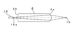
ところで、このような受信用の光モジュール7においては、受光素子10の受光面がシリコーン等によって形成されているため、図12に示すように、光ファイバ15の端部15aから出射された光(同図破線部)が、受光素子10の受光面において反射されることによって、光ファイバ15の端部15aに戻り光(同図二点差線部)として戻って(入射して)しまうことが問題となっていた。このような戻り光は、特に、シングルモード方式の光ファイバ15を用いる場合においては、ノイズとなって送信側のデバイスの光出力特性に悪影響を与える虞があった。
このような問題を低減するためには、例えば、図13に示すように、光電変換装置8をレンズ2の光軸OAに対して傾けた状態で光電変換装置取付部3に取り付けることによって、受光素子10の受光面における光の反射方向を、反射光の光ファイバ15の端部15aへの入射(入射光量)が抑制され得る方向(端部15aから可及的に外れる方向)に制御することが考えられる。
また、これ以外にも、従来から、戻り光の問題を低減するための種々の提案がなされている。
例えば、特許文献1においては、PDチップを斜めに実装した光電変換装置を用いることによって、PDチップからの反射光が戻り光となることを抑制することが提案されている。
また、特許文献2においては、光ファイバの端部を、これの光軸をレンズの光軸に対して傾けた状態で取り付けることによって、PDの反射光がレンズを透過した後に戻り光となることを抑制することが提案されている。
しかしながら、図13の構成は、光電変換装置8における光電変換装置取付部3への当接面(図13におけるステム9の上面)が、光電変換装置取付部3における光電変換装置8の当接面(図13における下端面3a)に対して傾いた状態となるため、光電変換装置8を接着剤18を介して光電変換装置取付部3に安定的に当接させることができず、正確な調芯作業(受光素子10の受光面の中心点をレンズ2の光軸OA上に位置合わせする作業、以下同様)も困難となってしまう。すなわち、図13の構成は、光電変換装置8の取り付けを簡便かつ高精度に行うことができないといった問題点を有している。
また、特許文献1に記載の構成は、PDチップが傾いた特殊な光電変換装置(カスタマイズ品)を用いなければならないため、コストが高くなるといった問題点を有している。
さらに、特許文献2に記載の構成は、光ファイバを斜めに保持する必要上、光レセプタクルを、光ファイバを保持する部分とレンズおよび光電変換装置を保持する部分とで個別に製造しなければならない。蓋し、両部分を金型を用いて一体成形しようとしても、光ファイバを保持する部分が傾いているため、離型を確保するための金型設計が非常に困難となるからである。すなわち、特許文献2に記載の構成は、光レセプタクルを簡便かつ安価に製造することができないといった問題点を有している。更に、こればかりでなく、特許文献2に記載の構成は、光ファイバを斜めに保持する構成上、温度変化にともなう光レセプタクルの寸法変化(線膨脹)によって、受光素子に対するファイバ光の結合効率が大きく変化する虞があるといった光学性能上の問題点も有している。
そこで、本発明は、このような問題点に鑑みなされたものであり、戻り光を有効に低減することができるとともに、光学性能の確保、製造の効率化および低コスト化を図ることができる光レセプタクルおよびこれを備えた光モジュールを提供することを目的とするものである。
前述した目的を達成するため、本発明の請求項1に係る光レセプタクルの特徴は、光ファイバの端部を取り付けるための筒状の光ファイバ取付部と、受光素子を有する光電変換装置を当接させた状態で取り付けるための筒状の光電変換装置取付部と、前記光ファイバの端部と前記受光素子とを光学的に結合するためのレンズとを備えた光レセプタクルにおいて、前記光ファイバ取付部、前記光電変換装置取付部および前記レンズは、透光性の樹脂材料によって一体的に形成され、前記光ファイバ取付部は、前記レンズの光軸と同心状に形成され、前記光電変換装置取付部における前記光電変換装置の当接面が、前記レンズの光軸に垂直な平面に対して傾きを有するように形成され、前記光電変換装置として、前記光電変換装置取付部への当接面が前記受光素子の受光面に平行とされたものが取り付けられる点にある。
そして、この請求項1に係る発明によれば、光電変換装置取付部における光電変換装置の当接面を、レンズの光軸に垂直な平面に対して傾きを有するように形成することにより、汎用的な光電変換装置を用いつつ、受光素子の受光面における反射光が戻り光となることを有効に低減することができ、かつ、光電変換装置取付部がレンズの光軸と同心であることによって、樹脂材料を用いた一体成形を無理なく行うことができるとともに温度変化に対する光学性能の安定性を確保することができ、さらに、光電変換装置取付部の当接面と光電変換装置の当接面とを安定的に当接させることによって、光電変換装置を簡便かつ高精度に取り付けることができる。
また、請求項2に係る光レセプタクルの特徴は、請求項1において、更に、前記光電変換装置取付部における前記光電変換装置の当接面は、前記光電変換装置取付部における前記光電変換装置側の端面である点にある。
そして、この請求項2に係る発明によれば、光電変換装置取付部よりも外周が大きな光電変換装置の取り付けに適切に対応することができる。
さらに、請求項3に係る光レセプタクルの特徴は、請求項1において、更に、前記光電変換装置取付部における前記光電変換装置の当接面は、前記光電変換装置取付部における前記光電変換装置側の端面よりも径方向における内側の位置において前記端面に対して前記レンズ側に凹入された凹入面である点にある。
そして、この請求項3に係る発明によれば、光電変換装置取付部よりも外周が小さな光電変換装置の取り付けに適切に対応することができる。
さらにまた、請求項4に係る光モジュールの特徴は、請求項1~3のいずれか1項に記載の光レセプタクルと、請求項1に記載の光ファイバと、請求項1に記載の光電変換装置とを備えた点にある。
そして、この請求項4に係る発明によれば、汎用的な光電変換装置を用いつつ、受光素子の受光面における反射光が戻り光となることを有効に低減することができ、かつ、樹脂材料を用いた光レセプタクルの一体成形を無理なく行うことができるとともに温度変化に対する光学性能の安定性を確保することができ、さらに、光電変換装置を簡便かつ高精度に取り付けることができる。
また、請求項5に係る光モジュールの特徴は、請求項4において、更に、前記光ファイバは、シングルモード光ファイバである点にある。
そして、この請求項5に係る発明によれば、マルチモード光ファイバを用いる場合に比較して、戻り光を低減する効果が顕著になる。
本発明によれば、戻り光を有効に低減することができるとともに、光学性能の確保、製造の効率化および低コスト化を図ることができる。
(第1実施形態)
以下、本発明の第1実施形態について、図1および図2を参照して説明する。
以下、本発明の第1実施形態について、図1および図2を参照して説明する。
ただし、従来と基本的な構成が同一もしくはこれに類する箇所については、同一の符号を用いて説明する。
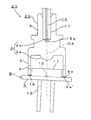
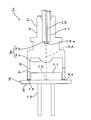
図1に示すように、本実施形態における光レセプタクル20は、従来の光レセプタクル1と同様に、レンズ2、光電変換装置取付部3’および光ファイバ取付部5が、透光性の樹脂材料を用いて一体的に形成されることによって構成されている。また、本実施形態における光レセプタクル20は、特許文献2に記載の構成とは異なり、光ファイバ取付部5が、レンズ2の光軸OAと同心状に形成されているため、金型を用いて無理なく一体成形することができる。因みに、金型としては、例えば、光ファイバ取付部5の内周面ならびに上端面およびレンズ2の平面2bの形状転写面が形成された上型(例えば、可動型)と、光電変換装置取付部3’の内周面ならびに下端面およびレンズ2の凸面2aの形状転写面が形成された下型(例えば、固定型)と、光レセプタクル20の外周面の形状転写面が形成され、光軸OAを含む仮想平面上にパーティングラインを有するようなスプリットモールドとを備えた射出成形金型を用いてもよい。この場合に、スプリットモールドは、光レセプタクル20の外周面における図1の左半部を成形するための左側のスライド型と、光レセプタクル20の外周面における図1の右半部を成形するための右側のスライド型と、各スライド型にそれぞれ備えられた貫通孔4を成形するためのピンとによって構成されたものであってもよい。
また、図10に示した従来の構成においては、光電変換装置取付部3における光電変換装置8の当接面である下端面3aが、レンズ2の光軸OAに垂直な仮想平面に対して平行に形成されていたが、本実施形態における光レセプタクル20は、そのような従来の構成とは異なっている。
すなわち、図1に示すように、本実施形態においては、光電変換装置取付部3’における光電変換装置8の当接面としての光電変換装置取付部3’の下端面3a’が、レンズ2の光軸OAに垂直な仮想平面Sに対して傾きを有するように形成されている。より具体的には、光電変換装置取付部3’の下端面3a’は、光軸OAを囲む輪帯状を呈しているとともに、全周にわたって、レンズ2の光軸OAに垂直な仮想平面Sに対して所定の傾斜角を有する1つの仮想平面S’上(同一平面上)に配置されている。
そして、このような本実施形態の光レセプタクル20は、図2に示すように、光ファイバ取付部5への光ファイバ15の取り付けと、光電変換装置取付部3’への光電変換装置8の取り付けとを行うことによって、本実施形態における光モジュール21を構成するようになっている。
なお、光電変換装置8は、光電変換装置取付部3’への当接面としてのステム9の上端面9aが、受光素子10の受光面(上端面)に平行とされたものであり、このような光電変換装置8は、特許文献1に記載の構成とは異なり、汎用品(既存品)として比較的安価に入手できるものである。光電変換装置8の取り付けは、具体的には、光電変換装置8の受光素子10およびキャップ11を、光電変換装置取付部3’によって囲まれた空間内に挿入させるようにして、光電変換装置8の当接面9aを、接着剤18(例えば、熱硬化性樹脂)を挟んで光電変換装置取付部3’の当接面3a’に当接させて、前述した調芯作業の後、接着剤18を硬化(例えば、熱硬化)することによって行われる。
図2に示すように、本実施形態における光モジュール21は、受光素子10の受光面が、レンズ2の凸面2aに正対してはおらず、所定の傾きを有している。このため、レンズ2から受光素子10に向けて出射された光(光ファイバ15によって送信側から伝送された光)は、受光面において反射されたとしても、この反射光の反射方向が、光ファイバ15の端部15aへの反射光の入射を可及的に抑制し得る方向に制御される。これにより、受光素子10の受光面における反射光が戻り光となることを有効に低減することができる。
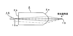
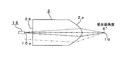
ここで、図3~図5には、レンズ2の光軸OAに垂直な仮想平面Sに対する受光素子10の受光面の傾き(すなわち、当接面3a’の傾き)が、それぞれ、2°、4°、6°となった場合における光ファイバ15の端部15aからの出射光の光路が示されている。なお、図3~図5中の破線は、光ファイバ15の端部15aからの出射光(但し、受光素子10の受光面に到達する前の段階のもの)を示しており、また、同各図中における二点差線は、受光素子10の受光面における出射光の反射光を示している。図3~図5に示すように、戻り光を低減するためには、受光素子10の受光面の傾きが大きい方が望ましいと言える。しかしながら、その一方で、受光面の傾きによって、受光面に対する光の結合効率が悪化することは望ましくない。この点について、本実施形態の構成では、受光素子10の受光面の傾きと光結合効率との相関関係についてのシミュレーションを行った場合には、図6に示すようなシミュレーション結果を得ることができる。なお、図6における横軸は、レンズ2の光軸OAに垂直な仮想平面Sに対する受光素子10としてのフォトディテクタの受光面の傾き(°)であり、縦軸は、フォトディテクタの受光面に対する光ファイバの出射光の結合効率(dB)である。また、図6のシミュレーションにおいては、光ファイバとして、NAが0.14、コア径がΦ0.01mmのものを用いるとともに、フォトディテクタとして、受光面がΦ0.05mmのものを用いた。図6に示すように、本実施形態によれば、受光面が30°傾いたとしても、十分な結合効率(-0.52dB)が得られることが分かる。このようなシミュレーション結果は、光ファイバ15の端部15aとレンズ2とが同軸状に配置されていることによるものと推測される。
なお、図10に示した従来の光レセプタクル1においても、図13に示したように受光素子10の受光面を傾けた状態で取り付けることによって戻り光の発生を防止することができるが、その場合に光電変換装置8の高精度な取り付けが困難となることは既に述べた通りである。
したがって、本実施形態によれば、汎用的な光電変換装置8を用いつつ、受光素子10の受光面における反射光が戻り光となることを有効に防止することができる。また、光電変換装置取付部3’がレンズ2の光軸OAと同心であることによって、樹脂材料を用いた光レセプタクル20の一体成形を無理なく行うことができるとともに、温度変化に対する光学性能の安定性を確保することができる。さらに、光電変換装置取付部3’の当接面3a’と光電変換装置8の当接面9aとを安定的に当接させることによって、光電変換装置8を簡便かつ高精度に取り付けることができる。ここで、図6に示したように、本実施形態によれば、受光素子10の受光面の傾きについては、ある程度の角度(少なくとも30°)までは光学性能上の安定性が確保されると言える。しかしながら、図6のシミュレーション結果は、前述の調芯作業が正確に行われたことが前提であるので、当接面3a’、9a同士を接着剤18を挟んで安定的に当接させて正確な調芯作業を行った上で光電変換装置8を光電変換装置取付部3’における所期の取り付け位置に高精度に取り付けることは、光学性能を確保する上で重要な要素である。特に、本実施形態においては、光電変換装置取付部3’よりも外周が大きい光電変換装置8の取り付けに適切に対応することができる。
これ以外にも、本実施形態における光レセプタクル20は、図10に示したような従来の光レセプタクル1の成形金型に対して、当接面3a’の形状転写面を形成するための軽微な加工を施したものを用いて成形することができる場合もある。このような場合には、既存の成形金型を活用することによって更なるコストの削減を図ることができる。
なお、上記以外の構成は、図10および図11に示したものと基本的に同様であるので、詳細は省略する。
(第2実施形態)
次に、本発明の第2実施形態について、第1実施形態との差異を中心として、図7および図8を参照して説明する。
次に、本発明の第2実施形態について、第1実施形態との差異を中心として、図7および図8を参照して説明する。
図7に示すように、本実施形態における光レセプタクル24は、光電変換装置取付部3”における光電変換装置8の当接面が、レンズ2の光軸OAに垂直な仮想平面Sに対して傾きを有するように形成されているという点では、第1実施形態と同様である。
ただし、本実施形態においては、図7に示すように、光電変換装置取付部3”における当接面が、光電変換装置取付部3”の下端面3a”ではなく、下端面3a”よりも径方向における内側の位置において下端面3a”に対してレンズ2側に凹入された凹入面3bとされている。
図8は、このような本実施形態の光レセプタクル24を備えた光モジュール25を示したものである。
図8に示すように、本実施形態においても、光電変換装置取付部3”における当接面3bと光電変換装置8における当接面9aとを当接させた状態で光電変換装置8を光電変換装置取付部3”に簡便かつ安定的に取り付けることによって、受光素子10の受光面をレンズ2に対して傾けることができる。
したがって、本実施形態においても、第1実施形態と同様の作用効果を奏することができる。特に、本実施形態においては、光電変換装置取付部3”よりも外周が小さい光電変換装置8の取り付けに適切に対応することができる。
なお、本発明は、前述した実施の形態に限定されるものではなく、本発明の特徴を損なわない限度において種々変更することができる。
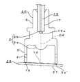
例えば、本発明は、CANパッケージ型の光電変換装置8に限らず、図9に示すように、半導体基板27の表面に受光素子10が実装された基板実装型の光電変換装置28にも有効に適用することができる。
2 レンズ
3’ 光電変換装置取付部
5 光ファイバ取付部
8 光電変換装置
15 光ファイバ
3’ 光電変換装置取付部
5 光ファイバ取付部
8 光電変換装置
15 光ファイバ
Claims (5)
- 光ファイバの端部を取り付けるための筒状の光ファイバ取付部と、
受光素子を有する光電変換装置を当接させた状態で取り付けるための筒状の光電変換装置取付部と、
前記光ファイバの端部と前記受光素子とを光学的に結合するためのレンズと
を備えた光レセプタクルにおいて、
前記光ファイバ取付部、前記光電変換装置取付部および前記レンズは、透光性の樹脂材料によって一体的に形成され、
前記光ファイバ取付部は、前記レンズの光軸と同心状に形成され、
前記光電変換装置取付部における前記光電変換装置の当接面が、前記レンズの光軸に垂直な平面に対して傾きを有するように形成され、
前記光電変換装置として、前記光電変換装置取付部への当接面が前記受光素子の受光面に平行とされたものが取り付けられること
を特徴とする光レセプタクル。 - 前記光電変換装置取付部における前記光電変換装置の当接面は、前記光電変換装置取付部における前記光電変換装置側の端面であること
を特徴とする請求項1に記載の光レセプタクル。 - 前記光電変換装置取付部における前記光電変換装置の当接面は、前記光電変換装置取付部における前記光電変換装置側の端面よりも径方向における内側の位置において前記端面に対して前記レンズ側に凹入された凹入面であること
を特徴とする請求項1に記載の光レセプタクル。 - 請求項1~3のいずれか1項に記載の光レセプタクルと、
請求項1に記載の光ファイバと、
請求項1に記載の光電変換装置と
を備えたことを特徴とする光モジュール。 - 前記光ファイバは、シングルモード光ファイバであること
を特徴とする請求項4に記載の光モジュール。
Priority Applications (2)
| Application Number | Priority Date | Filing Date | Title |
|---|---|---|---|
| US14/122,232 US9291783B2 (en) | 2011-06-07 | 2012-06-07 | Optical receptacle and optical module provided with same |
| CN201280028085.3A CN103582837B (zh) | 2011-06-07 | 2012-06-07 | 光插座以及具备该光插座的光模块 |
Applications Claiming Priority (2)
| Application Number | Priority Date | Filing Date | Title |
|---|---|---|---|
| JP2011127181A JP2012252308A (ja) | 2011-06-07 | 2011-06-07 | 光レセプタクルおよびこれを備えた光モジュール |
| JP2011-127181 | 2011-06-07 |
Publications (1)
| Publication Number | Publication Date |
|---|---|
| WO2012169586A1 true WO2012169586A1 (ja) | 2012-12-13 |
Family
ID=47296141
Family Applications (1)
| Application Number | Title | Priority Date | Filing Date |
|---|---|---|---|
| PCT/JP2012/064685 Ceased WO2012169586A1 (ja) | 2011-06-07 | 2012-06-07 | 光レセプタクルおよびこれを備えた光モジュール |
Country Status (5)
| Country | Link |
|---|---|
| US (1) | US9291783B2 (ja) |
| JP (1) | JP2012252308A (ja) |
| CN (1) | CN103582837B (ja) |
| TW (1) | TWI544247B (ja) |
| WO (1) | WO2012169586A1 (ja) |
Cited By (1)
| Publication number | Priority date | Publication date | Assignee | Title |
|---|---|---|---|---|
| CN104216070A (zh) * | 2013-05-30 | 2014-12-17 | 恩普乐股份有限公司 | 光插座以及具有这种光插座的光模块 |
Families Citing this family (9)
| Publication number | Priority date | Publication date | Assignee | Title |
|---|---|---|---|---|
| JP2014232261A (ja) * | 2013-05-30 | 2014-12-11 | 株式会社エンプラス | 光レセプタクルおよびこれを備えた光モジュール |
| CN107735708B (zh) | 2015-07-02 | 2019-10-25 | 奥林巴斯株式会社 | 光信号传送系统和光插座 |
| JP6222182B2 (ja) * | 2015-07-31 | 2017-11-01 | 住友電気工業株式会社 | 波長多重光受信モジュール |
| JP6630226B2 (ja) * | 2016-04-27 | 2020-01-15 | 日立オートモティブシステムズ株式会社 | 撮像モジュールおよび撮像装置 |
| JP2018097032A (ja) * | 2016-12-08 | 2018-06-21 | 株式会社エンプラス | 光レセプタクル、光モジュールおよび光モジュールの製造方法 |
| JP2022001919A (ja) * | 2020-06-22 | 2022-01-06 | 三和電気工業株式会社 | 光モジュール及びその製造方法 |
| US11513300B2 (en) | 2020-12-30 | 2022-11-29 | Enplas Corporation | Optical receptacle and optical module |
| JP2023023940A (ja) * | 2021-08-06 | 2023-02-16 | 株式会社エンプラス | 光レセプタクル、光モジュールおよび光レセプタクルの製造方法 |
| CN115061248B (zh) * | 2022-07-25 | 2024-09-17 | 希烽光电科技(南京)有限公司 | 一种高响应度低回损的同轴器件的装配方法 |
Citations (4)
| Publication number | Priority date | Publication date | Assignee | Title |
|---|---|---|---|---|
| JPS56113305U (ja) * | 1980-01-30 | 1981-09-01 | ||
| JPS60138506A (ja) * | 1983-12-27 | 1985-07-23 | Toshiba Corp | 受光素子モジユ−ル |
| JPH0555563U (ja) * | 1991-12-24 | 1993-07-23 | 安藤電気株式会社 | 受光素子保持具 |
| JP2004239997A (ja) * | 2003-02-04 | 2004-08-26 | Enplas Corp | 光モジュール及びそれを備えた光コネクタ |
Family Cites Families (14)
| Publication number | Priority date | Publication date | Assignee | Title |
|---|---|---|---|---|
| US5526455A (en) * | 1993-09-17 | 1996-06-11 | Sumitomo Electric Industries, Ltd. | Connector including opposing lens surfaces, side surfaces, and contact surfaces for coupling optical devices |
| US5692083A (en) * | 1996-03-13 | 1997-11-25 | The Whitaker Corporation | In-line unitary optical device mount and package therefor |
| JPH1068843A (ja) * | 1996-08-27 | 1998-03-10 | Ando Electric Co Ltd | 高反射減衰量型受光装置 |
| DE19961624B4 (de) * | 1999-12-13 | 2005-01-20 | Infineon Technologies Ag | Kopplungsanordnung |
| US6607309B2 (en) * | 2001-06-01 | 2003-08-19 | Infineon Technologies Ag | Optical device |
| JP3954901B2 (ja) * | 2001-07-23 | 2007-08-08 | シャープ株式会社 | 光伝送用ジャックモジュールおよびプラグ・ジャック式光伝送装置 |
| US7083337B2 (en) * | 2002-10-30 | 2006-08-01 | Finisar Corporation | Optical transceiver port |
| DE10307763B4 (de) * | 2003-02-14 | 2005-06-09 | Infineon Technologies Ag | Elektro-optisches Modul zum Senden und/oder Empfangen optischer Signale mindestens zweier optischer Datenkanäle |
| JP2004294636A (ja) * | 2003-03-26 | 2004-10-21 | Enplas Corp | 光モジュールおよびこれを備えた光コネクタ |
| US20050018981A1 (en) * | 2003-07-23 | 2005-01-27 | Jds Uniphase Corporation | Receiver optical sub-assembly with reduced back reflection |
| FR2871244A1 (fr) * | 2004-06-07 | 2005-12-09 | Fci Sa | Dispositif de couplage optique |
| JP4965201B2 (ja) * | 2005-12-09 | 2012-07-04 | 株式会社エンプラス | 光モジュール用ホルダ、光モジュールおよび光コネクタ |
| JP2008083282A (ja) | 2006-09-27 | 2008-04-10 | Nippon Telegr & Teleph Corp <Ntt> | 光モジュール及びその調芯方法 |
| JP2009258365A (ja) | 2008-04-16 | 2009-11-05 | Mitsubishi Electric Corp | 光レセプタクル |
-
2011
- 2011-06-07 JP JP2011127181A patent/JP2012252308A/ja active Pending
-
2012
- 2012-06-01 TW TW101119798A patent/TWI544247B/zh not_active IP Right Cessation
- 2012-06-07 CN CN201280028085.3A patent/CN103582837B/zh active Active
- 2012-06-07 WO PCT/JP2012/064685 patent/WO2012169586A1/ja not_active Ceased
- 2012-06-07 US US14/122,232 patent/US9291783B2/en active Active
Patent Citations (4)
| Publication number | Priority date | Publication date | Assignee | Title |
|---|---|---|---|---|
| JPS56113305U (ja) * | 1980-01-30 | 1981-09-01 | ||
| JPS60138506A (ja) * | 1983-12-27 | 1985-07-23 | Toshiba Corp | 受光素子モジユ−ル |
| JPH0555563U (ja) * | 1991-12-24 | 1993-07-23 | 安藤電気株式会社 | 受光素子保持具 |
| JP2004239997A (ja) * | 2003-02-04 | 2004-08-26 | Enplas Corp | 光モジュール及びそれを備えた光コネクタ |
Cited By (1)
| Publication number | Priority date | Publication date | Assignee | Title |
|---|---|---|---|---|
| CN104216070A (zh) * | 2013-05-30 | 2014-12-17 | 恩普乐股份有限公司 | 光插座以及具有这种光插座的光模块 |
Also Published As
| Publication number | Publication date |
|---|---|
| CN103582837A (zh) | 2014-02-12 |
| US20140086536A1 (en) | 2014-03-27 |
| TW201303403A (zh) | 2013-01-16 |
| US9291783B2 (en) | 2016-03-22 |
| CN103582837B (zh) | 2016-08-17 |
| TWI544247B (zh) | 2016-08-01 |
| JP2012252308A (ja) | 2012-12-20 |
Similar Documents
| Publication | Publication Date | Title |
|---|---|---|
| US9291783B2 (en) | Optical receptacle and optical module provided with same | |
| CN104364689B (zh) | 用于耦合光纤输入/输出的具有结构化反射表面的耦合装置 | |
| CN103676032B (zh) | 连接器及其制造方法和光学通信系统 | |
| US20040033033A1 (en) | Optical module | |
| US9645330B2 (en) | Optical module | |
| JP2004239997A (ja) | 光モジュール及びそれを備えた光コネクタ | |
| TWI553364B (zh) | 光電轉換器 | |
| JP2002043675A (ja) | 光モジュール | |
| WO2010007861A1 (ja) | 光コネクタ | |
| JP6207881B2 (ja) | 光レセプタクルおよびこれを備えた光モジュール | |
| US11768339B2 (en) | Optical receptacle and optical module | |
| JP5749592B2 (ja) | 光レセプタクルおよびこれを備えた光モジュール | |
| WO2014156630A1 (ja) | 光通信用のレンズ及び光通信モジュール | |
| CN106030363A (zh) | 光插座和光模块 | |
| WO2014045850A1 (ja) | 光通信用のレンズ及び光通信モジュール | |
| JP2007279561A (ja) | 光送受信モジュール用ホルダ | |
| US9250400B2 (en) | Optical receptacle and optical module including the same | |
| JP2012237819A (ja) | 光モジュール用フォルダ | |
| JP4952219B2 (ja) | 光モジュール | |
| JP2008004916A (ja) | 光モジュール | |
| JP2014197086A (ja) | 光通信用モジュール又は光通信ユニット | |
| JP2009258154A (ja) | 光送信モジュールとその製造方法 | |
| KR101959501B1 (ko) | 수동 광정렬 패키징된 광전모듈 및 그 제조방법 | |
| JP2011118274A (ja) | 光レセプタクル | |
| WO2009154160A1 (ja) | 光コネクタ |
Legal Events
| Date | Code | Title | Description |
|---|---|---|---|
| 121 | Ep: the epo has been informed by wipo that ep was designated in this application |
Ref document number: 12796060 Country of ref document: EP Kind code of ref document: A1 |
|
| WWE | Wipo information: entry into national phase |
Ref document number: 14122232 Country of ref document: US |
|
| NENP | Non-entry into the national phase |
Ref country code: DE |
|
| 122 | Ep: pct application non-entry in european phase |
Ref document number: 12796060 Country of ref document: EP Kind code of ref document: A1 |