WO2012165403A1 - 有機薄膜、その製造方法、及びそれを有する有機トランジスタ - Google Patents
有機薄膜、その製造方法、及びそれを有する有機トランジスタ Download PDFInfo
- Publication number
- WO2012165403A1 WO2012165403A1 PCT/JP2012/063702 JP2012063702W WO2012165403A1 WO 2012165403 A1 WO2012165403 A1 WO 2012165403A1 JP 2012063702 W JP2012063702 W JP 2012063702W WO 2012165403 A1 WO2012165403 A1 WO 2012165403A1
- Authority
- WO
- WIPO (PCT)
- Prior art keywords
- thin film
- organic thin
- plasma
- film
- liquid crystal
- Prior art date
Links
- 239000010409 thin film Substances 0.000 title claims abstract description 108
- 238000004519 manufacturing process Methods 0.000 title claims abstract description 20
- 239000004973 liquid crystal related substance Substances 0.000 claims abstract description 94
- 150000001875 compounds Chemical class 0.000 claims abstract description 80
- 238000006116 polymerization reaction Methods 0.000 claims abstract description 62
- 239000000203 mixture Substances 0.000 claims abstract description 52
- 239000010408 film Substances 0.000 claims description 129
- 238000000576 coating method Methods 0.000 claims description 93
- 239000011248 coating agent Substances 0.000 claims description 89
- 238000000034 method Methods 0.000 claims description 48
- 239000003505 polymerization initiator Substances 0.000 claims description 46
- IJGRMHOSHXDMSA-UHFFFAOYSA-N Atomic nitrogen Chemical compound N#N IJGRMHOSHXDMSA-UHFFFAOYSA-N 0.000 claims description 23
- 229920000642 polymer Polymers 0.000 claims description 17
- 239000012986 chain transfer agent Substances 0.000 claims description 13
- 239000007869 azo polymerization initiator Substances 0.000 claims description 11
- 229910001873 dinitrogen Inorganic materials 0.000 claims description 9
- 239000003960 organic solvent Substances 0.000 claims description 9
- 239000003999 initiator Substances 0.000 claims description 8
- XLYOFNOQVPJJNP-UHFFFAOYSA-N water Substances O XLYOFNOQVPJJNP-UHFFFAOYSA-N 0.000 claims description 8
- 230000001678 irradiating effect Effects 0.000 claims description 7
- 239000000243 solution Substances 0.000 description 27
- 230000000052 comparative effect Effects 0.000 description 24
- 239000011261 inert gas Substances 0.000 description 17
- 239000007788 liquid Substances 0.000 description 16
- 230000007704 transition Effects 0.000 description 16
- 239000004065 semiconductor Substances 0.000 description 15
- 239000004990 Smectic liquid crystal Substances 0.000 description 13
- 239000012298 atmosphere Substances 0.000 description 12
- 239000007789 gas Substances 0.000 description 12
- 239000002904 solvent Substances 0.000 description 12
- 238000009281 ultraviolet germicidal irradiation Methods 0.000 description 12
- 239000011521 glass Substances 0.000 description 10
- 230000015572 biosynthetic process Effects 0.000 description 9
- 238000011156 evaluation Methods 0.000 description 9
- QVGXLLKOCUKJST-UHFFFAOYSA-N atomic oxygen Chemical compound [O] QVGXLLKOCUKJST-UHFFFAOYSA-N 0.000 description 8
- 238000001723 curing Methods 0.000 description 8
- 238000010438 heat treatment Methods 0.000 description 8
- 229910052757 nitrogen Inorganic materials 0.000 description 8
- 239000001301 oxygen Substances 0.000 description 8
- 229910052760 oxygen Inorganic materials 0.000 description 8
- 238000009832 plasma treatment Methods 0.000 description 8
- 230000008569 process Effects 0.000 description 8
- 239000000126 substance Substances 0.000 description 8
- 238000012719 thermal polymerization Methods 0.000 description 8
- 238000000137 annealing Methods 0.000 description 6
- 239000000463 material Substances 0.000 description 6
- 230000003287 optical effect Effects 0.000 description 6
- 230000001105 regulatory effect Effects 0.000 description 6
- -1 oxime esters Chemical class 0.000 description 5
- 238000004528 spin coating Methods 0.000 description 5
- OZAIFHULBGXAKX-UHFFFAOYSA-N 2-(2-cyanopropan-2-yldiazenyl)-2-methylpropanenitrile Chemical compound N#CC(C)(C)N=NC(C)(C)C#N OZAIFHULBGXAKX-UHFFFAOYSA-N 0.000 description 4
- ZWEHNKRNPOVVGH-UHFFFAOYSA-N 2-Butanone Chemical compound CCC(C)=O ZWEHNKRNPOVVGH-UHFFFAOYSA-N 0.000 description 4
- 125000000751 azo group Chemical group [*]N=N[*] 0.000 description 4
- 238000002425 crystallisation Methods 0.000 description 4
- 230000008025 crystallization Effects 0.000 description 4
- 125000005647 linker group Chemical group 0.000 description 4
- 238000002156 mixing Methods 0.000 description 4
- 239000012299 nitrogen atmosphere Substances 0.000 description 4
- 239000000047 product Substances 0.000 description 4
- 239000000758 substrate Substances 0.000 description 4
- UHOVQNZJYSORNB-UHFFFAOYSA-N Benzene Chemical compound C1=CC=CC=C1 UHOVQNZJYSORNB-UHFFFAOYSA-N 0.000 description 3
- VYZAMTAEIAYCRO-UHFFFAOYSA-N Chromium Chemical compound [Cr] VYZAMTAEIAYCRO-UHFFFAOYSA-N 0.000 description 3
- YMWUJEATGCHHMB-UHFFFAOYSA-N Dichloromethane Chemical compound ClCCl YMWUJEATGCHHMB-UHFFFAOYSA-N 0.000 description 3
- ZMXDDKWLCZADIW-UHFFFAOYSA-N N,N-Dimethylformamide Chemical compound CN(C)C=O ZMXDDKWLCZADIW-UHFFFAOYSA-N 0.000 description 3
- CBENFWSGALASAD-UHFFFAOYSA-N Ozone Chemical compound [O-][O+]=O CBENFWSGALASAD-UHFFFAOYSA-N 0.000 description 3
- JUJWROOIHBZHMG-UHFFFAOYSA-N Pyridine Chemical group C1=CC=NC=C1 JUJWROOIHBZHMG-UHFFFAOYSA-N 0.000 description 3
- 239000000654 additive Substances 0.000 description 3
- 230000008901 benefit Effects 0.000 description 3
- 238000006243 chemical reaction Methods 0.000 description 3
- 229910052804 chromium Inorganic materials 0.000 description 3
- 239000011651 chromium Substances 0.000 description 3
- 238000009792 diffusion process Methods 0.000 description 3
- 208000037265 diseases, disorders, signs and symptoms Diseases 0.000 description 3
- 230000000694 effects Effects 0.000 description 3
- VLKZOEOYAKHREP-UHFFFAOYSA-N n-Hexane Chemical compound CCCCCC VLKZOEOYAKHREP-UHFFFAOYSA-N 0.000 description 3
- 238000002360 preparation method Methods 0.000 description 3
- 239000005268 rod-like liquid crystal Substances 0.000 description 3
- CSCPPACGZOOCGX-UHFFFAOYSA-N Acetone Chemical compound CC(C)=O CSCPPACGZOOCGX-UHFFFAOYSA-N 0.000 description 2
- QGZKDVFQNNGYKY-UHFFFAOYSA-N Ammonia Chemical compound N QGZKDVFQNNGYKY-UHFFFAOYSA-N 0.000 description 2
- 229920002799 BoPET Polymers 0.000 description 2
- HEDRZPFGACZZDS-UHFFFAOYSA-N Chloroform Chemical compound ClC(Cl)Cl HEDRZPFGACZZDS-UHFFFAOYSA-N 0.000 description 2
- 229920000742 Cotton Polymers 0.000 description 2
- XTHFKEDIFFGKHM-UHFFFAOYSA-N Dimethoxyethane Chemical compound COCCOC XTHFKEDIFFGKHM-UHFFFAOYSA-N 0.000 description 2
- IAZDPXIOMUYVGZ-UHFFFAOYSA-N Dimethylsulphoxide Chemical compound CS(C)=O IAZDPXIOMUYVGZ-UHFFFAOYSA-N 0.000 description 2
- 239000004985 Discotic Liquid Crystal Substance Chemical class 0.000 description 2
- LFQSCWFLJHTTHZ-UHFFFAOYSA-N Ethanol Chemical compound CCO LFQSCWFLJHTTHZ-UHFFFAOYSA-N 0.000 description 2
- 239000004642 Polyimide Substances 0.000 description 2
- WYURNTSHIVDZCO-UHFFFAOYSA-N Tetrahydrofuran Chemical compound C1CCOC1 WYURNTSHIVDZCO-UHFFFAOYSA-N 0.000 description 2
- 238000003848 UV Light-Curing Methods 0.000 description 2
- 230000009471 action Effects 0.000 description 2
- 125000004432 carbon atom Chemical group C* 0.000 description 2
- 230000008859 change Effects 0.000 description 2
- 230000003098 cholesteric effect Effects 0.000 description 2
- 238000007796 conventional method Methods 0.000 description 2
- 238000004132 cross linking Methods 0.000 description 2
- 238000000354 decomposition reaction Methods 0.000 description 2
- 238000007607 die coating method Methods 0.000 description 2
- HJUFTIJOISQSKQ-UHFFFAOYSA-N fenoxycarb Chemical compound C1=CC(OCCNC(=O)OCC)=CC=C1OC1=CC=CC=C1 HJUFTIJOISQSKQ-UHFFFAOYSA-N 0.000 description 2
- 230000005669 field effect Effects 0.000 description 2
- 239000007888 film coating Substances 0.000 description 2
- 238000009501 film coating Methods 0.000 description 2
- 238000001914 filtration Methods 0.000 description 2
- 239000005357 flat glass Substances 0.000 description 2
- PCHJSUWPFVWCPO-UHFFFAOYSA-N gold Chemical compound [Au] PCHJSUWPFVWCPO-UHFFFAOYSA-N 0.000 description 2
- 229910052737 gold Inorganic materials 0.000 description 2
- 239000010931 gold Substances 0.000 description 2
- 238000007756 gravure coating Methods 0.000 description 2
- 230000001771 impaired effect Effects 0.000 description 2
- 230000006872 improvement Effects 0.000 description 2
- 230000005764 inhibitory process Effects 0.000 description 2
- 150000002576 ketones Chemical class 0.000 description 2
- 238000000206 photolithography Methods 0.000 description 2
- 108091008695 photoreceptors Proteins 0.000 description 2
- 229920001721 polyimide Polymers 0.000 description 2
- 239000011148 porous material Substances 0.000 description 2
- 238000010526 radical polymerization reaction Methods 0.000 description 2
- 238000004544 sputter deposition Methods 0.000 description 2
- QNODIIQQMGDSEF-UHFFFAOYSA-N (1-hydroxycyclohexyl)-phenylmethanone Chemical compound C=1C=CC=CC=1C(=O)C1(O)CCCCC1 QNODIIQQMGDSEF-UHFFFAOYSA-N 0.000 description 1
- IMQFZQVZKBIPCQ-UHFFFAOYSA-N 2,2-bis(3-sulfanylpropanoyloxymethyl)butyl 3-sulfanylpropanoate Chemical compound SCCC(=O)OCC(CC)(COC(=O)CCS)COC(=O)CCS IMQFZQVZKBIPCQ-UHFFFAOYSA-N 0.000 description 1
- BXYWKXBAMJYTKP-UHFFFAOYSA-N 2-[2-[2-[2-(3-sulfanylpropanoyloxy)ethoxy]ethoxy]ethoxy]ethyl 3-sulfanylpropanoate Chemical compound SCCC(=O)OCCOCCOCCOCCOC(=O)CCS BXYWKXBAMJYTKP-UHFFFAOYSA-N 0.000 description 1
- UHFFVFAKEGKNAQ-UHFFFAOYSA-N 2-benzyl-2-(dimethylamino)-1-(4-morpholin-4-ylphenyl)butan-1-one Chemical compound C=1C=C(N2CCOCC2)C=CC=1C(=O)C(CC)(N(C)C)CC1=CC=CC=C1 UHFFVFAKEGKNAQ-UHFFFAOYSA-N 0.000 description 1
- SUODCTNNAKSRHB-UHFFFAOYSA-N 2-ethylhexyl 3-sulfanylpropanoate Chemical compound CCCCC(CC)COC(=O)CCS SUODCTNNAKSRHB-UHFFFAOYSA-N 0.000 description 1
- XMLYCEVDHLAQEL-UHFFFAOYSA-N 2-hydroxy-2-methyl-1-phenylpropan-1-one Chemical compound CC(C)(O)C(=O)C1=CC=CC=C1 XMLYCEVDHLAQEL-UHFFFAOYSA-N 0.000 description 1
- LWRBVKNFOYUCNP-UHFFFAOYSA-N 2-methyl-1-(4-methylsulfanylphenyl)-2-morpholin-4-ylpropan-1-one Chemical compound C1=CC(SC)=CC=C1C(=O)C(C)(C)N1CCOCC1 LWRBVKNFOYUCNP-UHFFFAOYSA-N 0.000 description 1
- 125000003903 2-propenyl group Chemical group [H]C([*])([H])C([H])=C([H])[H] 0.000 description 1
- DKIDEFUBRARXTE-UHFFFAOYSA-N 3-mercaptopropanoic acid Chemical compound OC(=O)CCS DKIDEFUBRARXTE-UHFFFAOYSA-N 0.000 description 1
- UUEWCQRISZBELL-UHFFFAOYSA-N 3-trimethoxysilylpropane-1-thiol Chemical compound CO[Si](OC)(OC)CCCS UUEWCQRISZBELL-UHFFFAOYSA-N 0.000 description 1
- 239000004342 Benzoyl peroxide Substances 0.000 description 1
- OMPJBNCRMGITSC-UHFFFAOYSA-N Benzoylperoxide Chemical compound C=1C=CC=CC=1C(=O)OOC(=O)C1=CC=CC=C1 OMPJBNCRMGITSC-UHFFFAOYSA-N 0.000 description 1
- DKPFZGUDAPQIHT-UHFFFAOYSA-N Butyl acetate Natural products CCCCOC(C)=O DKPFZGUDAPQIHT-UHFFFAOYSA-N 0.000 description 1
- XDTMQSROBMDMFD-UHFFFAOYSA-N Cyclohexane Chemical group C1CCCCC1 XDTMQSROBMDMFD-UHFFFAOYSA-N 0.000 description 1
- YIVJZNGAASQVEM-UHFFFAOYSA-N Lauroyl peroxide Chemical compound CCCCCCCCCCCC(=O)OOC(=O)CCCCCCCCCCC YIVJZNGAASQVEM-UHFFFAOYSA-N 0.000 description 1
- 239000004988 Nematic liquid crystal Substances 0.000 description 1
- 239000004677 Nylon Substances 0.000 description 1
- 239000002202 Polyethylene glycol Substances 0.000 description 1
- 239000004372 Polyvinyl alcohol Substances 0.000 description 1
- XBDQKXXYIPTUBI-UHFFFAOYSA-M Propionate Chemical compound CCC([O-])=O XBDQKXXYIPTUBI-UHFFFAOYSA-M 0.000 description 1
- 208000034189 Sclerosis Diseases 0.000 description 1
- VYPSYNLAJGMNEJ-UHFFFAOYSA-N Silicium dioxide Chemical compound O=[Si]=O VYPSYNLAJGMNEJ-UHFFFAOYSA-N 0.000 description 1
- CDBYLPFSWZWCQE-UHFFFAOYSA-L Sodium Carbonate Chemical compound [Na+].[Na+].[O-]C([O-])=O CDBYLPFSWZWCQE-UHFFFAOYSA-L 0.000 description 1
- 239000004974 Thermotropic liquid crystal Substances 0.000 description 1
- 239000007875 V-40 Substances 0.000 description 1
- AVTLBBWTUPQRAY-BUHFOSPRSA-N V-59 Substances CCC(C)(C#N)\N=N\C(C)(CC)C#N AVTLBBWTUPQRAY-BUHFOSPRSA-N 0.000 description 1
- 239000007877 V-601 Substances 0.000 description 1
- WYGWHHGCAGTUCH-ISLYRVAYSA-N V-65 Substances CC(C)CC(C)(C#N)\N=N\C(C)(C#N)CC(C)C WYGWHHGCAGTUCH-ISLYRVAYSA-N 0.000 description 1
- 239000007874 V-70 Substances 0.000 description 1
- 239000007878 VAm-110 Substances 0.000 description 1
- YAAUVJUJVBJRSQ-UHFFFAOYSA-N [3-(3-sulfanylpropanoyloxy)-2-[[3-(3-sulfanylpropanoyloxy)-2,2-bis(3-sulfanylpropanoyloxymethyl)propoxy]methyl]-2-(3-sulfanylpropanoyloxymethyl)propyl] 3-sulfanylpropanoate Chemical compound SCCC(=O)OCC(COC(=O)CCS)(COC(=O)CCS)COCC(COC(=O)CCS)(COC(=O)CCS)COC(=O)CCS YAAUVJUJVBJRSQ-UHFFFAOYSA-N 0.000 description 1
- KXKVLQRXCPHEJC-UHFFFAOYSA-N acetic acid trimethyl ester Natural products COC(C)=O KXKVLQRXCPHEJC-UHFFFAOYSA-N 0.000 description 1
- 125000003647 acryloyl group Chemical group O=C([*])C([H])=C([H])[H] 0.000 description 1
- 230000004913 activation Effects 0.000 description 1
- 230000000996 additive effect Effects 0.000 description 1
- 125000000217 alkyl group Chemical group 0.000 description 1
- 150000001350 alkyl halides Chemical class 0.000 description 1
- 125000002947 alkylene group Chemical group 0.000 description 1
- 125000003368 amide group Chemical group 0.000 description 1
- 150000001408 amides Chemical class 0.000 description 1
- 229910021529 ammonia Inorganic materials 0.000 description 1
- 125000003118 aryl group Chemical group 0.000 description 1
- 230000004888 barrier function Effects 0.000 description 1
- 150000001555 benzenes Chemical group 0.000 description 1
- 235000019400 benzoyl peroxide Nutrition 0.000 description 1
- 238000007664 blowing Methods 0.000 description 1
- RFAZFSACZIVZDV-UHFFFAOYSA-N butan-2-one Chemical compound CCC(C)=O.CCC(C)=O RFAZFSACZIVZDV-UHFFFAOYSA-N 0.000 description 1
- 229910052799 carbon Inorganic materials 0.000 description 1
- 125000003178 carboxy group Chemical group [H]OC(*)=O 0.000 description 1
- 239000003153 chemical reaction reagent Substances 0.000 description 1
- 239000013626 chemical specie Substances 0.000 description 1
- 239000003795 chemical substances by application Substances 0.000 description 1
- 239000013065 commercial product Substances 0.000 description 1
- 238000011437 continuous method Methods 0.000 description 1
- 230000001276 controlling effect Effects 0.000 description 1
- 239000003431 cross linking reagent Substances 0.000 description 1
- 230000007547 defect Effects 0.000 description 1
- 238000000151 deposition Methods 0.000 description 1
- 238000010586 diagram Methods 0.000 description 1
- 238000003618 dip coating Methods 0.000 description 1
- 238000007606 doctor blade method Methods 0.000 description 1
- WNAHIZMDSQCWRP-UHFFFAOYSA-N dodecane-1-thiol Chemical compound CCCCCCCCCCCCS WNAHIZMDSQCWRP-UHFFFAOYSA-N 0.000 description 1
- 238000001035 drying Methods 0.000 description 1
- 150000002148 esters Chemical class 0.000 description 1
- 150000002170 ethers Chemical class 0.000 description 1
- 230000005284 excitation Effects 0.000 description 1
- 230000001747 exhibiting effect Effects 0.000 description 1
- 238000007765 extrusion coating Methods 0.000 description 1
- 239000004744 fabric Substances 0.000 description 1
- 230000002349 favourable effect Effects 0.000 description 1
- 239000012847 fine chemical Substances 0.000 description 1
- 239000003205 fragrance Substances 0.000 description 1
- 125000003827 glycol group Chemical group 0.000 description 1
- 238000007646 gravure printing Methods 0.000 description 1
- 150000004820 halides Chemical class 0.000 description 1
- 150000002391 heterocyclic compounds Chemical class 0.000 description 1
- FUZZWVXGSFPDMH-UHFFFAOYSA-N hexanoic acid Chemical compound CCCCCC(O)=O FUZZWVXGSFPDMH-UHFFFAOYSA-N 0.000 description 1
- 229930195733 hydrocarbon Natural products 0.000 description 1
- 150000002430 hydrocarbons Chemical class 0.000 description 1
- 230000002209 hydrophobic effect Effects 0.000 description 1
- 125000002887 hydroxy group Chemical group [H]O* 0.000 description 1
- 238000003475 lamination Methods 0.000 description 1
- 239000012528 membrane Substances 0.000 description 1
- 229910052751 metal Inorganic materials 0.000 description 1
- 239000002184 metal Substances 0.000 description 1
- LDTLDBDUBGAEDT-UHFFFAOYSA-N methyl 3-sulfanylpropanoate Chemical compound COC(=O)CCS LDTLDBDUBGAEDT-UHFFFAOYSA-N 0.000 description 1
- 238000012986 modification Methods 0.000 description 1
- 230000004048 modification Effects 0.000 description 1
- 125000001624 naphthyl group Chemical group 0.000 description 1
- 125000002560 nitrile group Chemical group 0.000 description 1
- 125000006574 non-aromatic ring group Chemical group 0.000 description 1
- 229920001778 nylon Polymers 0.000 description 1
- KZCOBXFFBQJQHH-UHFFFAOYSA-N octane-1-thiol Chemical compound CCCCCCCCS KZCOBXFFBQJQHH-UHFFFAOYSA-N 0.000 description 1
- LWNSNYBMYBWJDN-UHFFFAOYSA-N octyl 3-sulfanylpropanoate Chemical compound CCCCCCCCOC(=O)CCS LWNSNYBMYBWJDN-UHFFFAOYSA-N 0.000 description 1
- 239000012788 optical film Substances 0.000 description 1
- 125000000962 organic group Chemical group 0.000 description 1
- 150000001451 organic peroxides Chemical class 0.000 description 1
- 229920000620 organic polymer Polymers 0.000 description 1
- MPQXHAGKBWFSNV-UHFFFAOYSA-N oxidophosphanium Chemical class [PH3]=O MPQXHAGKBWFSNV-UHFFFAOYSA-N 0.000 description 1
- 125000004430 oxygen atom Chemical group O* 0.000 description 1
- 125000001997 phenyl group Chemical group [H]C1=C([H])C([H])=C(*)C([H])=C1[H] 0.000 description 1
- 229920001223 polyethylene glycol Polymers 0.000 description 1
- 229920006254 polymer film Polymers 0.000 description 1
- 230000000379 polymerizing effect Effects 0.000 description 1
- 229920002451 polyvinyl alcohol Polymers 0.000 description 1
- 229910052573 porcelain Inorganic materials 0.000 description 1
- 238000007639 printing Methods 0.000 description 1
- 238000012545 processing Methods 0.000 description 1
- 230000001737 promoting effect Effects 0.000 description 1
- UMJSCPRVCHMLSP-UHFFFAOYSA-N pyridine Natural products COC1=CC=CN=C1 UMJSCPRVCHMLSP-UHFFFAOYSA-N 0.000 description 1
- 238000007763 reverse roll coating Methods 0.000 description 1
- 238000007789 sealing Methods 0.000 description 1
- 229910052814 silicon oxide Inorganic materials 0.000 description 1
- 238000005507 spraying Methods 0.000 description 1
- 125000005504 styryl group Chemical group 0.000 description 1
- 150000003462 sulfoxides Chemical class 0.000 description 1
- 229910052717 sulfur Inorganic materials 0.000 description 1
- 125000004434 sulfur atom Chemical group 0.000 description 1
- 238000004381 surface treatment Methods 0.000 description 1
- 239000004094 surface-active agent Substances 0.000 description 1
- YLQBMQCUIZJEEH-UHFFFAOYSA-N tetrahydrofuran Natural products C=1C=COC=1 YLQBMQCUIZJEEH-UHFFFAOYSA-N 0.000 description 1
- 230000008719 thickening Effects 0.000 description 1
- 238000003852 thin film production method Methods 0.000 description 1
- 125000003396 thiol group Chemical group [H]S* 0.000 description 1
- 238000013519 translation Methods 0.000 description 1
- 125000005580 triphenylene group Chemical group 0.000 description 1
- 238000007740 vapor deposition Methods 0.000 description 1
- 230000000007 visual effect Effects 0.000 description 1
Images

Classifications
-
- C—CHEMISTRY; METALLURGY
- C08—ORGANIC MACROMOLECULAR COMPOUNDS; THEIR PREPARATION OR CHEMICAL WORKING-UP; COMPOSITIONS BASED THEREON
- C08F—MACROMOLECULAR COMPOUNDS OBTAINED BY REACTIONS ONLY INVOLVING CARBON-TO-CARBON UNSATURATED BONDS
- C08F2/00—Processes of polymerisation
- C08F2/46—Polymerisation initiated by wave energy or particle radiation
- C08F2/48—Polymerisation initiated by wave energy or particle radiation by ultraviolet or visible light
- C08F2/50—Polymerisation initiated by wave energy or particle radiation by ultraviolet or visible light with sensitising agents
-
- H—ELECTRICITY
- H10—SEMICONDUCTOR DEVICES; ELECTRIC SOLID-STATE DEVICES NOT OTHERWISE PROVIDED FOR
- H10K—ORGANIC ELECTRIC SOLID-STATE DEVICES
- H10K10/00—Organic devices specially adapted for rectifying, amplifying, oscillating or switching; Organic capacitors or resistors having potential barriers
- H10K10/40—Organic transistors
- H10K10/46—Field-effect transistors, e.g. organic thin-film transistors [OTFT]
-
- H—ELECTRICITY
- H10—SEMICONDUCTOR DEVICES; ELECTRIC SOLID-STATE DEVICES NOT OTHERWISE PROVIDED FOR
- H10K—ORGANIC ELECTRIC SOLID-STATE DEVICES
- H10K71/00—Manufacture or treatment specially adapted for the organic devices covered by this subclass
- H10K71/10—Deposition of organic active material
- H10K71/191—Deposition of organic active material characterised by provisions for the orientation or alignment of the layer to be deposited
-
- H—ELECTRICITY
- H10—SEMICONDUCTOR DEVICES; ELECTRIC SOLID-STATE DEVICES NOT OTHERWISE PROVIDED FOR
- H10K—ORGANIC ELECTRIC SOLID-STATE DEVICES
- H10K85/00—Organic materials used in the body or electrodes of devices covered by this subclass
- H10K85/10—Organic polymers or oligomers
- H10K85/111—Organic polymers or oligomers comprising aromatic, heteroaromatic, or aryl chains, e.g. polyaniline, polyphenylene or polyphenylene vinylene
- H10K85/113—Heteroaromatic compounds comprising sulfur or selene, e.g. polythiophene
-
- H—ELECTRICITY
- H10—SEMICONDUCTOR DEVICES; ELECTRIC SOLID-STATE DEVICES NOT OTHERWISE PROVIDED FOR
- H10K—ORGANIC ELECTRIC SOLID-STATE DEVICES
- H10K85/00—Organic materials used in the body or electrodes of devices covered by this subclass
- H10K85/60—Organic compounds having low molecular weight
- H10K85/649—Aromatic compounds comprising a hetero atom
- H10K85/655—Aromatic compounds comprising a hetero atom comprising only sulfur as heteroatom
-
- H—ELECTRICITY
- H10—SEMICONDUCTOR DEVICES; ELECTRIC SOLID-STATE DEVICES NOT OTHERWISE PROVIDED FOR
- H10K—ORGANIC ELECTRIC SOLID-STATE DEVICES
- H10K85/00—Organic materials used in the body or electrodes of devices covered by this subclass
- H10K85/731—Liquid crystalline materials
Definitions
- the present invention relates to an organic thin film useful for various applications such as an optical compensation film and an organic semiconductor film, a method for producing the same, and an organic transistor having the same.
- an organic thin film prepared by fixing the orientation of a polymerizable liquid crystal compound by polymerization is used for various applications such as an optical compensation film of a liquid crystal display device.
- the organic thin film is generally formed by aligning a polymerizable liquid crystal compound and then irradiating light or heat to advance a polymerization reaction to fix the alignment.
- a technique for forming a multilayer organic thin film has been demanded for high functionality.
- mixing of the upper layer and the lower layer may be a problem.
- Patent Documents 1 and 2 have been proposed to use plasma for the polymerization reaction.
- An object of the present invention is to provide a technique that can improve both the degree of orientation and the degree of hardening of an organic thin film formed using a polymerizable liquid crystal compound.
- Another object of the present invention is to provide an organic thin film having a high degree of orientation and a high degree of film hardening, a method for producing the same, and an organic transistor having the same.
- Means for solving the above problems are as follows.
- the technique which enables the improvement of both the orientation degree and the hardening degree of the organic thin film formed using a polymeric liquid crystal compound can be provided.
- the organic thin film which has high orientation degree property and high film thickness, its manufacturing method, and an organic transistor which has it can be provided.
- a numerical range represented by using “to” means a range including numerical values described before and after “to” as a lower limit value and an upper limit value.
- organic thin film is used in the sense of including both a self-supporting organic thin film, and a layer and a film formed on the support.
- composition containing at least one polymerizable liquid crystal compound refers to a composition composed of only at least one polymerizable liquid crystal compound, and at least one polymerizable liquid crystal compound, It shall be used in the meaning of including a composition containing one or more additives such as a polymerization initiator and a chain transfer agent.
- polymerizable liquid crystal compound is used to mean not only a compound showing a liquid crystal phase alone but also a compound having a liquid crystal group (mesogen group) showing a liquid crystal phase in the presence of an additive.
- the present invention relates to an organic thin film obtained by fixing the orientation of a composition containing at least one polymerizable liquid crystal compound by polymerization by plasma irradiation.
- the polymerization is advanced by irradiating a plasma gas introduced into the discharge space.
- the plasma includes various active species generated by the decomposition, excitation, activation, radicalization, ionization, and the like of the gas introduced into the discharge space. Therefore, even if the composition does not contain a polymerization initiator, or even if the ratio of the polymerization initiator in the composition is small, the polymerizable liquid crystal compound is activated by plasma irradiation to cause a polymerization reaction.
- the polymerizable liquid crystal compound is brought into a predetermined alignment state (at the same time as the alignment state), the polymerization reaction is advanced by plasma irradiation, or the polymerizable liquid crystal compound is brought into a predetermined alignment state,
- the polymerization reaction is advanced by plasma irradiation to fix the orientation and form an organic thin film. It has not been known so far that the polymerization reaction can proceed while maintaining the alignment state of the liquid crystal by plasma polymerization, which is different from conventional photopolymerization and thermal polymerization. This is the findings. Moreover, it is an unexpected effect that the obtained organic thin film has improved orientation as compared with an organic thin film of the same material formed by photopolymerization or thermal polymerization.
- the polymerization reaction proceeds by plasma irradiation
- plasma irradiation means, for example, that the composition is aligned and the composition is irradiated with plasma to advance the polymerization reaction (that is, a predetermined reaction)
- the composition is irradiated with plasma to advance the polymerization reaction (that is, , After aligning most of the composition (specifically, 90% or more of the composition, more preferably 95% or more, most preferably 100% of the composition) to a predetermined state, and then polymerizing by plasma irradiation A mode of promoting the reaction).
- the polymerization is advanced by plasma irradiation, there is no need for a polymerization initiator.
- the film in the case of an organic thin film having a thin film thickness, specifically, a film thickness of 50 nm or less, the film can be sufficiently hardened even without a polymerization initiator.
- the polymerizable liquid crystal compound is preferably plasma polymerized in the presence of at least one of a polymerization initiator and a chain transfer agent.
- the addition amount of the polymerization initiator or the chain transfer agent is 10% by mass or less based on the polymerizable liquid crystal compound. It is preferably 0.2 to 5% by mass, more preferably 0.2 to 2% by mass. However, it is not limited to this range.
- the kind of polymerization initiator which can be used for this invention is not restriction
- a suitable type can be selected according to the nature of the irradiated plasma and the type of plasma generating gas.
- the polymerization initiator of the present invention it is preferable to use a photopolymerization initiator or a thermal polymerization initiator.
- the photopolymerization initiator a known photopolymerization initiator can be used.
- the photopolymerization initiator that can be used in the present invention is a UV plasma that emits UV light because nitrogen plasma using nitrogen gas emits UV light. It is more preferable to use a UV polymerization initiator that generates radicals and the like.
- UV polymerization initiators such as ⁇ -amino ketones, ⁇ -hydroxy ketones, phosphine oxides, oxime esters, and titanocenes can be used.
- Commercially available products for example, IRSFACURE907, DAROCURE1173, IRGACURE184, IRGACURE369, IRGACURE379, IRGACURE819, IRGACURE784, IRGACURE OXE01, IRGACURE OXE02, etc.
- IRSFACURE907 for example, IRSFACURE907, DAROCURE1173, IRGACURE184, IRGACURE369, IRGACURE379, IRGACURE819, IRGACURE784, IRGACURE OXE01, IRGACURE OXE02, etc.
- Thermal polymerization initiators that generate radicals by heat include organic peroxides such as lauroyl peroxide and benzoyl peroxide; azo-based polymerization initiators including azobisisobutyronitrile (AIBN), V-30, V-40, V-59, V-65, V-70, V-601, VF-096, VAm-110, VAm-111 (manufactured by Wako Pure Chemical Industries, Ltd.) and the like can be used.
- organic peroxides such as lauroyl peroxide and benzoyl peroxide
- azo-based polymerization initiators including azobisisobutyronitrile (AIBN), V-30, V-40, V-59, V-65, V-70, V-601, VF-096, VAm-110, VAm-111 (manufactured by Wako Pure Chemical Industries, Ltd.) and the like can be used.
- AIBN azobisisobutyronitrile
- the composition containing the polymerizable liquid crystal compound is controlled in a predetermined alignment state.
- a coating liquid in which a polymerizable liquid crystal compound is dissolved in a solvent is prepared, and the coating liquid is applied to the surface of the alignment film, or further heated as desired to remove the solvent.
- the orientation state can be controlled. Therefore, normally, the coating film containing the solvent together with the polymerizable liquid crystal compound is irradiated with plasma.
- plasma irradiation is performed on the coating film, unevenness occurs on the coating film surface due to the plasma gas (coating surface). May result in loss of transparency and increased haze.
- a polymer that contributes to an increase in the viscosity of the coating liquid is used as at least one of the polymerization initiator and the chain transfer agent.
- the polymerization initiator it is preferable to use a polymer polymerization initiator, and a more preferable polymerization initiator includes a polymer azo polymerization initiator.
- Examples of the polymer azo polymerization initiator of the present invention include a repeating unit composed of an azo group and a polymer unit (for example, a polydimethylsiloxane unit, a polyethylene glycol unit, etc.) introduced at both ends of the azo group.
- a polymer unit for example, a polydimethylsiloxane unit, a polyethylene glycol unit, etc.
- high molecular azo polymerization initiators having The molecular weight of the polymer unit is preferably 2000 to 10,000, and more preferably 5000 to 10,000.
- Specific examples of the polymer azo polymerization initiator are variously described in “Fine Chemical Vol. 39, No. 9, 47-52, 2010” and the like, and can be referred to.
- Commercial products for example, VPS-1001, VPE-0201, VPE-0401, VPE-0601, manufactured by Wako Pure Chemical Industries, Ltd. may be used.
- a chain transfer agent suitable for the polymerizable liquid crystal compound used in combination can be selected.
- a compound having a mercapto group can be selected. Specifically, 3-mercaptopropyltrimethoxysilane, ⁇ -mercaptopropionic acid, methyl-3-mercaptopropionate, 2-ethylhexyl-3-mercaptopro Pionate, n-octyl-3-mercaptopropionate, n-octyl mercaptan, n-dodecyl mercaptan, trimethylolpropane tris (3-mercaptopropionate), tris-[(3-mercaptopropionyloxy) -ethyl] -Isocyanurate, tetraethylene glycol bis (3-mercaptopropionate), dipentaerythritol hexakis (3-mercaptopropionate)
- the polymerizable liquid crystal compound that can be used in the present invention is not particularly limited.
- a thermotropic liquid crystal is preferable in terms of easy alignment control.
- liquid crystal compounds are generally classified into rod-like liquid crystal compounds and discotic liquid crystal compounds based on their molecular shapes, but liquid crystals of any molecular shape can be used in the present invention.
- a liquid crystal compound that transitions to any liquid crystal phase such as a nematic phase, a smectic A phase and a C phase, a cholesteric phase, a discotic nematic phase, or the like can also be used.
- the polymerization reaction can proceed while maintaining the high orientation of the liquid crystal phase. Therefore, when a liquid crystal compound that transitions to a liquid crystal phase with higher orientation is used, the liquid crystal The phase can be fixed, which may be advantageous for function expression. Specifically, a rod-like liquid crystal compound that can be transferred to a smectic A phase or a C phase may be suitable for the present invention, but is not limited to this example.
- the polymerizable liquid crystal compound generally has in its molecule a mother nucleus for exhibiting liquid crystallinity, a polymerizable group, and a linking group for linking the mother nucleus and the polymerizable group.
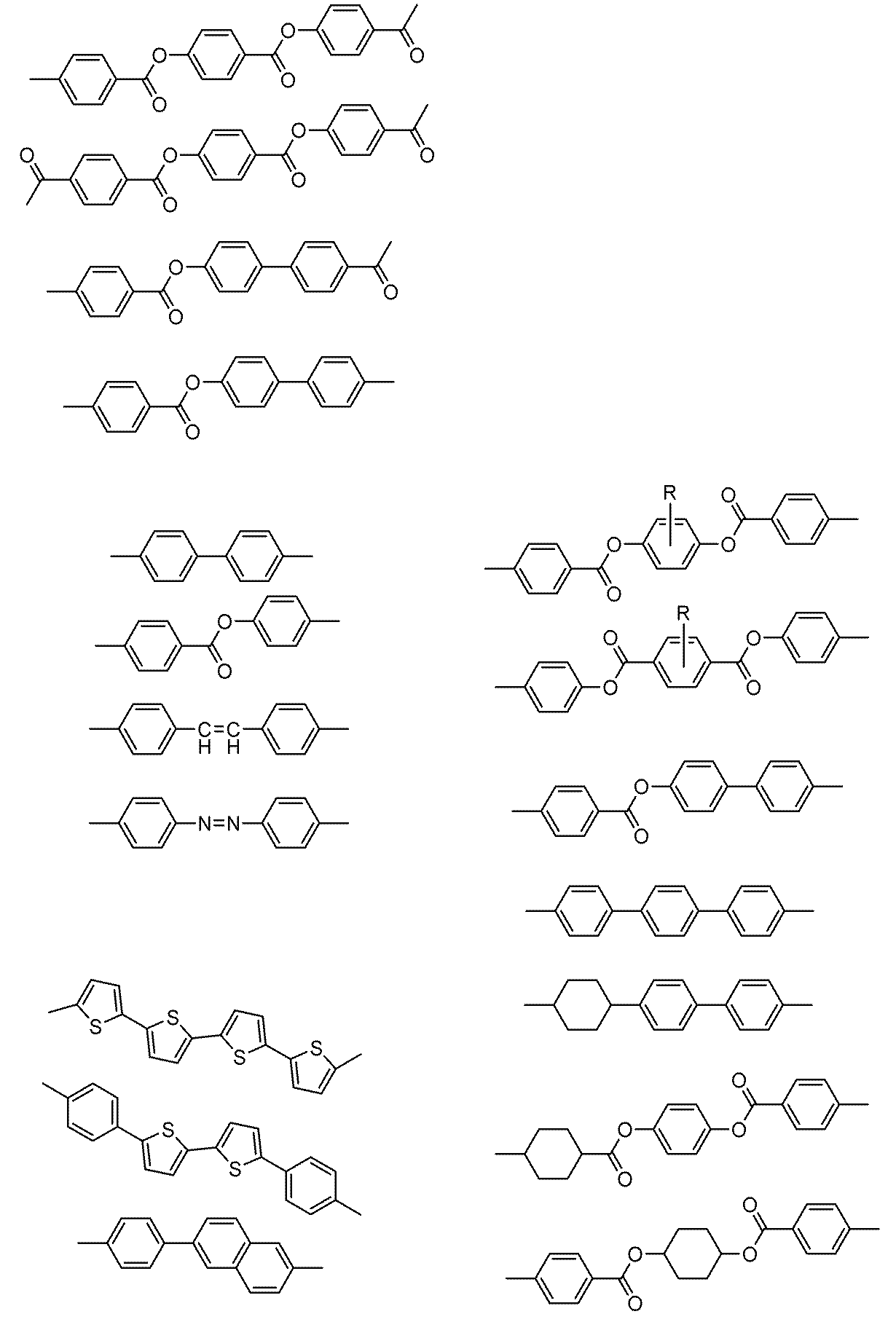
- the mother nucleus is a so-called mesogenic group, and examples thereof include Patent Documents: Japanese Patent No. 3416638, Japanese Patent Application Laid-Open No. 2006-259212, Japanese Patent No. 4493313, Japanese Translation of PCT International Publication No. 2008-537634, and Die Makromolekulare Chemie, Vol. 190, 2255-2268. (1989) and the like, and can be referred to in the present invention.
- Examples of the mother nucleus of the discotic liquid crystal compound include a discotic mother nucleus such as a triphenylene ring or a trisubstituted benzene ring, and examples of the mother nucleus of the rod-like liquid crystal compound include a plurality of (for example, 3 to 5) fragrances.
- An aromatic ring for example, a benzene ring, a naphthalene ring, a pyridine ring, etc.
- a non-aromatic ring for example, a cyclohexane ring
- a linking group for example, —COO—, —OCO—, —O—.
- the linking group is an organic group for bonding one or more to the mother nucleus and linking one or more polymerizable groups to the mother nucleus.
- Examples of the linking group include C 1 to C 20 alkylene groups (provided that one carbon atom or two or more carbon atoms not adjacent to each other are an oxygen atom, a sulfur atom, —COO—, OCO—, —NHCO).
- —, —CONH—, or —CO— may be substituted, and one —CH 2 —CH 2 — or two or more non-adjacent —CH 2 —CH 2 — may be represented by —CH ⁇ CH—, Or may be replaced by -C ⁇ C-).
- polymerizable group examples include ethylenic polymerizable groups such as methacryloyl group and acryloyl group, allyl group, styryl group and the like.
- ethylenic polymerizable groups such as methacryloyl group and acryloyl group, allyl group, styryl group and the like.
- a polymerizable liquid crystal compound having two or more polymerizable groups in one molecule.
- a non-liquid crystalline cross-linking agent having a plurality of polymerizable groups in the molecule may be added.
- polymerizable liquid crystal compound various polymerizable liquid crystal compounds that have been conventionally used for producing an optical compensation film of a liquid crystal display device can be used.
- a polymerizable liquid crystal compound conventionally used for forming an organic semiconductor film can be used as the polymerizable liquid crystal compound.
- An example is an oligothiophene liquid crystal compound.
- the oligothiophene-based polymerizable liquid crystal compounds there are compounds capable of forming a smectic phase, which are suitable as the material of the present invention.
- the composition used in the method for producing an organic thin film of the present invention may contain only one type of polymerizable liquid crystal compound or may contain two or more types of polymerizable liquid crystal compounds. Moreover, as above-mentioned, it is preferable to contain at least one of a polymerization initiator and a chain transfer agent. Further, the composition may contain one or more additives such as an alignment control agent for controlling the alignment of the liquid crystal compound and a surfactant for improving the coating suitability. However, the composition preferably contains a polymerizable liquid crystal compound as a main component, more preferably 95% by mass or more, or 98% by mass or more.
- An example of the method for producing an organic thin film of the present invention includes aligning a composition containing at least one polymerizable liquid crystal compound, aligning the composition, or after aligning the composition, and then applying plasma to the composition.
- This is a method for producing an organic thin film, which comprises irradiating and advancing polymerization to fix the orientation.
- the composition is preferably prepared as a coating solution.
- An organic solvent can be used.
- organic solvents that can be used include amides (eg, N, N-dimethylformamide), sulfoxides (eg, dimethyl sulfoxide), heterocyclic compounds (eg, pyridine), hydrocarbons (eg, benzene, hexane), alkyls Includes halides (eg, chloroform, dichloromethane), esters (eg, methyl acetate, butyl acetate), ketones (eg, acetone, methyl ethyl ketone (2-butanone)), ethers (eg, tetrahydrofuran, 1,2-dimethoxyethane) . Alkyl halides and ketones are preferred. Two or more organic solvents may be used in combination.
- a desired alignment state can be obtained by applying the composition on an alignment film such as a rubbing alignment film and heating and drying as desired.
- an alignment film such as a rubbing alignment film and heating and drying as desired.
- Various polymers such as a polymer for a polyvinyl alcohol alignment film and a polymer for a polyimide alignment film can be used.
- alignment films having various alignment regulating capabilities such as an alignment film having horizontal alignment regulating capability and an alignment film having vertical alignment regulating capability can be used.
- the means for expressing the alignment regulating force is not particularly limited, and for example, any of a rubbing alignment film showing alignment regulating ability by rubbing treatment and a photo-alignment film showing alignment regulating ability by light irradiation can be used.
- the composition can be applied by a general application method, for example, a spin coating method, an extrusion coating method, a direct gravure coating method, a reverse gravure coating method, or a die coating method.
- a general application method for example, a spin coating method, an extrusion coating method, a direct gravure coating method, a reverse gravure coating method, or a die coating method.
- orientation of the composition an orientation capable of expressing optical characteristics suitable for the application is selected according to the application.
- Various orientations such as a horizontal orientation, a vertical orientation, a hybrid orientation, and a cholesteric orientation can be selected.
- the temperature at which the nematic phase is formed is about 30 to 250 ° C. Therefore, when fixing the nematic phase, it is preferable to heat within the above temperature range.
- the temperature at which the smectic phase is formed is about 30 to 200 ° C. when the smectic phase is fixed, and it is preferable to heat within the above temperature range.
- the phase transition temperature varies depending on the type of liquid crystal, it is not limited to these ranges.
- the orientation control time that is, the heating time, an appropriate time is selected according to the film thickness, the film area, and the like. Generally, it is about 1 minute to 60 minutes.
- the coating film is irradiated with plasma to advance the polymerization reaction.
- a non-equilibrium plasma jet, low-temperature plasma by AC pulse discharge, or the like can be used, and it is preferable to use atmospheric pressure plasma generated under conditions near atmospheric pressure.
- Various atmospheric pressure plasma apparatuses can be used for plasma irradiation.
- an apparatus that can generate low-temperature plasma by performing intermittent discharge while passing an inert gas at a pressure close to atmospheric pressure between electrodes covered with a dielectric is preferable, and various modifications can be made depending on the purpose of use. You can choose an example. More specifically, in Japanese Patent Application Laid-Open No. 2008-60115, an apparatus used for substrate plasma processing, an atmospheric pressure plasma apparatus described in Japanese Patent Application Laid-Open No. 2004-228136, Japanese Patent Application Laid-Open No. 2006-21972, Japanese Patent Application Laid-Open No.
- the atmospheric pressure plasma apparatus is also available as a commercial product, for example, ATMP-1000 from Arios Co., Ltd., atmospheric pressure plasma apparatus from HEIDEN LABORATORIES, INC., S5000 type atmospheric pressure low-temperature plasma from Sakai Semiconductor Co., Ltd.
- Atmospheric pressure plasma devices currently on the market such as jet devices, MyPL100, ILP-1500 of Well Co., Ltd., and RD550 of Sekisui Chemical Co., Ltd. can also be suitably used.
- a pulse control element is used to supply current to the discharge part described in the specifications of WO2005 / 062338 and WO2007 / 024134. It is preferable to use a device with an electric circuit devised such as via.
- pressure near atmospheric pressure in “atmospheric pressure plasma” refers to a range of 70 kPa to 130 kPa, preferably 90 kPa to 110 kPa.
- a mixed gas such as the atmosphere can be used, but an inert gas such as He and Ar, or a rare gas such as He or Ar, or a nitrogen gas (N 2 ) (hereinafter referred to as these). It may be preferable to use simply “inert gas” in some cases, and He or N 2 is particularly preferable.
- active species for example, radicals contained in the plasma adhere to the surface of the coating film, and polymerization (for example, radical polymerization) starts from the surface. That is, in radical polymerization under normal atmosphere, tackiness (adhesiveness) occurs on the surface of the coating due to inhibition of polymerization by oxygen, but in plasma polymerization, coating is performed due to the high degree of polymerization on the surface of the coating. No tackiness (adhesiveness) occurs on the film surface.
- the polymerization reaction by the UV light irradiation can be advanced together with the progress of the polymerization reaction by the plasma irradiation. Further, when UV irradiation is performed simultaneously with or before plasma irradiation, the degree of hardening is further improved, which is advantageous for forming a film having a large thickness. It is particularly preferable to perform plasma irradiation after UV irradiation. When performing nitrogen plasma irradiation and / or when UV irradiation is used in combination, it is preferable to add a light (UV) polymerization initiator (a polymerization initiator that generates radicals by UV irradiation) to the composition. .
- UV light
- plasma irradiation may be performed in a batch method or in an in-line method connected to other processes.
- the plasma action site and the discharge site are separated, or the local concentration of the plasma (streamer) is suppressed by devising the discharge circuit, and uniform plasma
- the latter is preferable in that uniform plasma irradiation (plasma treatment) can be performed over a large area.
- a method in which the plasma generated by the discharge is brought into contact with the surface of the coating film by an inert gas stream is preferable, and a so-called plasma jet method is particularly preferable.
- the path (conducting tube) for transporting the inert gas containing plasma is preferably made of a dielectric such as glass, porcelain, or organic polymer.
- the distance from the supply nozzle of the inert gas containing plasma to the coating film surface is preferably 0.01 mm to 100 mm, and more preferably 1 mm to 20 mm.
- plasma can be applied to the surface of the coating film by an in-line system, similar to the system described in WO2009 / 096785. That is, a coating film for forming an organic thin film is formed by a coating method, and a blowing nozzle that can apply an inert gas and plasma to the coating film surface is provided on the downstream side of the coating process. Formation is possible.
- the polymerization reaction and the curing reaction start and proceed efficiently by direct action of plasma on the polymerizable liquid crystal compound present in the coating film. Even if the polymerization reaction which requires the closed system environment of an inert gas atmosphere as an objective is performed by an open system, it has the advantage that favorable sclerosis
- an inert gas may be sufficiently supplied to the region where the plasma treatment is performed, or the region may be filled with the inert gas.
- an inert gas is allowed to flow to the plasma generation site before the plasma is turned on, and the inert gas is allowed to continue even after the plasma is extinguished.
- the inert gas after the plasma treatment since the lifetime of the plasma is short, it may be exhausted without performing any special treatment, but the inert gas that has been treated by providing an inlet near the treatment area May be recovered.
- the temperature at the time of plasma irradiation can be selected arbitrarily depending on the characteristics of the material in the coating film irradiated with plasma, but damage can be reduced if the temperature rise caused by irradiation with atmospheric pressure plasma is smaller. preferable.
- the effect is further improved by separating the region to be subjected to the plasma treatment from the plasma generator.
- the supply of thermal energy from the plasma can be reduced and the temperature rise of the coating film can be suppressed by selecting and irradiating the atmospheric low temperature plasma.
- the temperature rise of the coating film due to the plasma irradiation is preferably 50 ° C. or less, more preferably 40 ° C. or less, and particularly preferably 20 ° C. or less.
- the temperature of the coating film at the time of plasma irradiation is preferably not higher than the temperature that the material in the coating film irradiated with plasma can withstand, and is generally preferably ⁇ 196 ° C. or higher and lower than 150 ° C. More preferably, it is not more than Particularly preferred is the vicinity of room temperature (25 ° C.) under an ambient temperature atmosphere.
- the organic thin film of the present invention formed by plasma irradiation has a high-density cross-linked structure and the degree of polymerization of the surface is high, a laminated (multilayer) structure was formed by a coating method. In some cases, unwanted diffusion / mixing into adjacent layers at the coating interface is also suppressed.
- the organic thin film production method of the present invention can be applied with an organic thin film having a multilayer structure because the compatibility and the diffusion of low molecular weight components at the interface with the adjacent layer, which are problems in the usual coating method, are suppressed. Even if formed by a method or a continuous method, it can be produced with high productivity.
- the surface hydrophilicity can be known using the contact angle of water as an index.
- the surface of the organic thin film of the present invention has a water contact angle (it is a contact angle when 2 ⁇ L of pure water is dropped and is preferably calculated as an average value of about 10 locations), and has a hydrophilicity of 80 ° or less. More preferably, it exhibits a hydrophilicity of 30 to 70 °, more preferably a hydrophilicity of 35 to 65 °.
- the liquid crystal compound is generally lipophilic, and the surface of a conventional cured film obtained by curing a composition containing a polymerizable liquid crystal compound as a main component by photopolymerization or thermal polymerization is generally hydrophobic.
- the organic thin film of the present invention is characterized in that it exhibits hydrophilicity (even if no surface treatment is performed), even though it contains a polymerizable liquid crystal compound as a main component.
- the thickness of the organic thin film of the present invention is not particularly limited. As described above, when an organic thin film having a small thickness, specifically, an organic thin film having a thickness of 50 nm or less is formed, the polymerization initiator may not be added. By the plasma irradiation, an organic thin film having a thickness of 50 to 2500 nm (more preferably 50 to 1000 nm, still more preferably 100 to 500 nm) can be stably produced.
- the organic thin film of the present invention may be formed on a support.
- a support a glass plate, a metal plate, various polymer films, and the like can be used.
- the present invention also relates to a method for producing a laminated film using the method for producing an organic thin film.
- the method for producing a laminated film of the present invention includes at least producing an organic thin film by the method and forming a film by applying a coating solution containing an organic solvent on the surface of the organic thin film. .
- the organic thin film produced by the above method is excellent in the degree of curing, particularly the degree of surface curing, and exhibits high solvent resistance.
- an upper layer film is formed by coating using a coating solution containing an organic solvent.
- undesired material diffusion / mixing does not occur at the coating interface.
- the method of the present invention is a laminate of organic thin films used for organic transistors such as organic TFTs and organic FETs, organic ELs, organic photoreceptors, etc., and a laminate in which the structure of the film interface affects the performance. It is advantageous to manufacture.
- organic transistors organic TFTs
- organic FETs such as organic FETs, organic EL, and organic photoreceptors.
- examples include spin coating, bar coating, spray coating, doctor blade method, dip coating, die coating, ink jet method, reverse roll coating, flexographic printing method, and gravure printing method.
- various organic solvents utilized in the said technical field can also be utilized also about the organic solvent used for a coating liquid.
- the organic thin film of the present invention can be used for various applications. It can utilize for optical films, such as an optical compensation film of a liquid crystal display device. Moreover, it can utilize as organic-semiconductor layers, such as an organic transistor. In particular, since a polymerization initiator serving as a carrier trap is unnecessary or the amount of use thereof can be reduced, an improvement in performance is expected. Since the influence of decomposition by plasma irradiation can be reduced, it is particularly effective as an organic semiconductor layer of a bottom-gate transistor.
- the present invention also relates to an organic transistor having the organic thin film of the present invention.
- One embodiment is an organic transistor having the organic thin film of the present invention as an organic semiconductor layer.
- Various conventionally known configurations can be employed.
- it is a bottom-gate transistor having the organic thin film of the present invention as an organic semiconductor layer and a gate electrode formed in the lower layer.
- FIG. 1 shows a schematic cross-sectional view of an example of a bottom-gate transistor, but the organic transistor of the present invention is not limited to this configuration.
- Other layers used in the organic transistor for example, each electrode layer, can be formed by an ordinary method by vapor-depositing chromium, gold or the like, and further using photolithography as necessary.
- the insulating film can also be formed by a conventional method using a sputtering method or the like.
- Example 1 (Orientation film formation) A horizontal alignment film coating solution SE-130 (product name of Nissan Chemical Industries, Ltd.) is formed on a blue plate glass (thickness: 1.1 mm) that has been subjected to UV ozone treatment by a spin coating method, and is applied to a hot plate at a temperature of 100 ° C. For 10 minutes. Next, a post-baking treatment was performed in a clean oven at a temperature of 210 ° C. for 1 hour to produce a glass having a horizontal alignment film formed thereon.
- SE-130 product name of Nissan Chemical Industries, Ltd.
- the rubbing process is performed using a rubbing apparatus RM-50 (trade name of EEC Sea) under the condition that the rubbing density (L) is 240 using nylon as the rubbing cloth, and the horizontal alignment subjected to the rubbing process.
- a glass with a film was prepared.
- a solution was prepared by dissolving 2 parts by mass of the polymerizable liquid crystal compound (1) shown below in 2-butanone for electronics industry (manufactured by Kanto Chemical). Next, this solution was filtered using a syringe filter having a pore size of 0.2 ⁇ m and used as a coating solution.
- the said coating liquid was apply
- the filtration and spin coating were performed in a glove box (dew point -40 ° C., oxygen concentration 1000 ppm or less, nitrogen gas atmosphere).
- the formed coating film was heat-treated (annealed) for 1 minute on a hot plate having a temperature shown in the following table in the air.
- the annealed coating film was irradiated with low-temperature N 2 plasma for 30 seconds using a S5000 type atmospheric pressure low-temperature plasma jet apparatus (discharge gas: nitrogen) manufactured by Sakai Semiconductor Co., Ltd., and the polymerization reaction was allowed to proceed to cure.
- a S5000 type atmospheric pressure low-temperature plasma jet apparatus discharge gas: nitrogen
- Sakai Semiconductor Co., Ltd. discharge gas: nitrogen
- Examples 2 to 7 In addition to 2 parts by mass of the polymerizable liquid crystal compound (1), a polymerization initiator or a chain transfer agent shown in the following table is dissolved in 0.04 parts by mass and 2-butanone to prepare a coating solution, and the temperature of the hot plate In addition, an organic thin film having a thickness of 500 nm was formed in the same manner as in Example 1 except that the types of plasma gas were changed as shown in the following table.
- the liquid crystal single molecule remains and exhibits the same phase transition temperature as that of the unpolymerized liquid crystal compound.
- the orientation of the liquid crystal compound is fixed in a state where the polymerization reaction has sufficiently progressed, no liquid crystal single molecule remains and no phase transition is observed.
- the transition temperature from the nematic liquid crystal phase to the isotropic phase is not observed even by heating at 240 degrees and is different from the phase transition behavior of the comparative example. From this, it can be understood that the cross-linking / fixing is performed while maintaining the alignment in the liquid crystal phase.
- the organic thin film of each example is a film cured with maintaining a high orientation with little light leakage, that is, no orientation defects due to orientation disorder. In Example 1, it is expected that the degree of polymerization inside the film is low because it is slightly darkened by heating.
- Examples 8 and 9 Organic thin films were prepared in the same manner as in Examples 1 and 2, except that the film thickness was changed to 100 nm and 60 nm, respectively. About each organic thin film, the solvent resistance was evaluated by the following method. Solvent resistance evaluation: The surface of each organic thin film was wiped off with a cotton swab containing ethanol, and the solvent resistance was evaluated. If nothing adhered to the cotton swab, it was evaluated that it had solvent resistance.
- Example 8 the polymerization initiator is not added (Example 8), or the addition amount of the polymerization initiator is small (Example 9), the solvent resistance is excellent. It can be understood that an organic thin film having a high hardness was obtained. About each organic thin film of Example 8 and 9, when orientation was evaluated similarly to the above, it was the same as the evaluation result of Example 1 and 2, respectively.
- Examples 10 and 11 Coating solutions were prepared in the same manner as in Examples 1 and 2 except that the following polymerizable liquid crystal compound (2) was used instead of the polymerizable liquid crystal compound (1).
- the following polymerizable liquid crystal compound (2) is a liquid crystal compound capable of forming a smectic phase, and the phase transition temperature from the smectic phase to the nematic phase was 129 ° C.
- the coating solution was applied to the rubbing-treated surface of the glass with a horizontal alignment film that was prepared in the same manner as in Example 1 to form a coating film.
- a horizontal alignment film that was prepared in the same manner as in Example 1 to form a coating film.
- plasma irradiation was performed in the same manner as in Examples 1 and 2, the polymerization reaction was advanced and cured, and an organic thin film having a thickness of 600 nm was formed.
- Comparative Example 4 A coating solution was prepared in the same manner as in Comparative Example 1 except that the polymerizable liquid crystal compound (2) was used in place of the polymerizable liquid crystal compound (1). In the same manner as described above, UV light was irradiated to advance the polymerization reaction, followed by curing to form an organic thin film having a thickness of 600 nm.
- the phase transition temperature and the orientation were evaluated.
- the adhesiveness of the surface was affixed to the treated film surface after a PET film (thickness: 50 ⁇ m) was peeled off, and the presence or absence of foreign matter on the PET film was checked with a digital microscope VHX-100 (Keyence). It was evaluated by observing using a product manufactured by the company. Being sticky means being in an uncured state. The results are shown in the table below.
- Examples 12 and 13 Comparative Example 5 (1)
- Examples 12 and 13 A coating solution was prepared in the same manner as in Examples 1 and 2 except that the following smectic liquid crystalline organic semiconductor was used instead of the polymerizable liquid crystal compound (1).
- the following smectic liquid crystalline organic semiconductor is a liquid crystalline organic semiconductor compound capable of forming a smectic phase.
- the coating solution was applied to the rubbed surface of the rubbed horizontal alignment film produced in the same manner as in Example 1 to form a coating film.
- the coating film was annealed at 90 ° C., plasma irradiation was performed in the same manner as in Examples 1 and 2, the polymerization reaction was allowed to proceed, and the organic thin film having a thickness of 100 nm was formed.
- Comparative Example 5 A coating solution was prepared in the same manner as in Comparative Example 1 except that the above smectic liquid crystalline organic semiconductor was used instead of the polymerizable liquid crystal compound (1).
- the organic thin film of Comparative Example 5 was formed by advancing the polymerization reaction by UV irradiation in the same manner as in Comparative Example 1 except that the annealing temperature condition was changed to 90 ° C. using this coating solution.
- the formed organic thin film of each Example can be polymerized while maintaining the orientation, has excellent solvent resistance, and can be understood to have a high hardness.
- the organic thin film is useful as an organic semiconductor layer of an organic transistor, particularly a bottom gate type organic transistor.
- the organic thin films of Examples 12 and 13 do not contain a polymerization initiator that causes carrier traps (Example 12) or only a small amount (Example 13), so high performance can be expected.
- the polymerization progressed during the annealing process in a nitrogen atmosphere and cured without being oriented.
- Example 14 (Production of organic transistors) A field effect organic transistor having the configuration shown in FIG. 1 was produced. Specifically, first, chromium was deposited on the alkali-free glass substrate 1 to form the gate electrode 2. Next, after an insulating film 3 made of 2000 angstroms of silicon oxide was formed by sputtering, vapor deposition was performed in the order of chromium and gold, and a source electrode 4 and a drain electrode 5 were formed by a normal photolithography technique.
- a polyimide thin film (LX-1400, manufactured by Hitachi Chemical DuPont Microsystems Co., Ltd.) is formed on the UV ozone-treated substrate, and a rubbing treatment is performed in the same manner as in Example 1 to form on the surface of the alignment film.
- a rubbing treatment is performed in the same manner as in Example 1 to form on the surface of the alignment film.
- an organic thin film to be a semiconductor active layer was produced.
- the electrical characteristics of the field effect transistor having a channel length of 10 ⁇ m, a channel width of 1 mm, and a semiconductor active layer thickness of about 0.2 ⁇ m manufactured by the above procedure were tested, and the current flowing between the source electrode and the drain electrode was It was observed with a semiconductor parameter analyzer 4155C (manufactured by Agilent) that it was modulated by the voltage applied to the electrodes.
- Examples 15 to 18 and Comparative Examples 6 to 8 were prepared by the above method.
- the coating film was formed.
- Example 15 only plasma irradiation under the following conditions was performed.
- Examples 16 to 18 after UV irradiation was performed under the following conditions, plasma irradiation was performed under the following conditions.
- Comparative Examples 6 to 8 only UV irradiation was performed under the following conditions.
- UV treatment Using UV curing chamber manufactured by Edmund Optics: ELC-500, UV irradiation was performed in the atmosphere for 10 minutes to cure.
- UV irradiation was performed in the atmosphere for 10 minutes to cure.
- the coating film hardened by UV irradiation is irradiated with low temperature N 2 plasma for 30 seconds using S5000 type atmospheric pressure low temperature plasma jet apparatus (discharge gas: nitrogen) manufactured by Sakai Semiconductor Co., Ltd. Advance and cure to form an organic thin film.
- phase transition temperature was measured in the same manner as described above, and the orientation evaluation and the tackiness were evaluated. The results are shown in the table below.
- Example 15 Although the orientation fixation in the nematic phase was observed, a phenomenon in which the visual field became dark was confirmed.
- the film thickness of the organic thin film is not only the same as Example 18 as Example 15, but also Examples 16 and 16 whose film thickness is significantly larger than Example 15.
- No. 17 no phase transition due to heating is observed, it is understood that the film is sufficiently cured because the orientation is sufficiently fixed and the adhesiveness on the surface of the organic thin film is lost.
- Example 19 ⁇ Immobilization of alignment on vertical alignment film> (Orientation film formation)
- a vertical alignment film coating solution SE-5300 (Nissan Chemical Industries trade name) is formed by a spin coat method, and then on a hot plate at a temperature of 100 ° C. For 10 minutes.
- a post-baking treatment was performed for 1 hour in a clean oven at a temperature of 210 ° C. to produce a glass on which a vertical alignment film was formed.
- the coating liquid (coating liquid containing a polymeric azo polymerization initiator) prepared in Example 5 was applied to the surface of the vertical alignment film to form a coating film.
- This coating film was stored in the atmosphere for 24 hours and the change of the coating film was observed visually, no crystallization occurred in this coating film.
- This coating film was irradiated with nitrogen plasma in the same manner as in Example 5 to form an organic thin film.
- the results of measuring the phase transition temperature and evaluating the orientation and adhesiveness in the same manner as above are shown in the following table.
- a coating film was formed on the surface of the vertical alignment film by applying the coating solution prepared in Example 1 (a coating solution containing a low molecular weight polymerization initiator). This coating film was also stored in the atmosphere for 24 hours in the same manner as in Example 19, and when the change of the coating film was visually observed, crystallization was observed in this coating film.
Landscapes
- Chemical & Material Sciences (AREA)
- Engineering & Computer Science (AREA)
- Materials Engineering (AREA)
- Polymers & Plastics (AREA)
- Health & Medical Sciences (AREA)
- Organic Chemistry (AREA)
- Physics & Mathematics (AREA)
- Spectroscopy & Molecular Physics (AREA)
- Medicinal Chemistry (AREA)
- Chemical Kinetics & Catalysis (AREA)
- Manufacturing & Machinery (AREA)
- Crystallography & Structural Chemistry (AREA)
- Polymerisation Methods In General (AREA)
- Liquid Deposition Of Substances Of Which Semiconductor Devices Are Composed (AREA)
- Thin Film Transistor (AREA)
- Liquid Crystal (AREA)
Abstract
高い配向性及び高い硬膜度を有する有機薄膜、及びその製造方法の提供。少なくとも1種の重合性液晶化合物を含有する組成物の配向を、プラズマ照射による重合により固定してなる有機薄膜である。また、少なくとも1種の重合性液晶化合物を含有する組成物を配向させること、前記組成物を配向させるとともに、又は配向させた後に、前記組成物にプラズマを照射して重合を進行させて、配向を固定すること、を含む有機薄膜の製造方法である。
Description
本発明は、光学補償膜、有機半導体膜等、種々の用途に有用な有機薄膜、並びにその製造方法及びそれを有する有機トランジスタに関する。
従来、重合性液晶化合物の配向を重合により固定して作製される有機薄膜が、液晶表示装置の光学補償膜等、種々の用途に用いられている。当該有機薄膜は、重合性液晶化合物を配向させた後、光や熱を照射して重合反応を進行させ、配向を固定して形成するのが一般的である。近年では、高機能化のために、有機薄膜を多層膜化する技術が求められている。有機薄膜の多層化では、上層と下層との混合が問題になる場合がある。上層と下層との混合を生じさせることなく多層化するためには、膜の硬度を改善する必要がある。しかし、形成される膜の硬度を改善するために重合開始剤の添加量を上げると、液晶の配向性が損なわれるという問題がある。また、重合反応の進行を阻害する酸素を排した不活性雰囲気下で上記製法を実施すると、液晶が完全に所望の配向状態になる前に重合反応が進行してしまい、液晶の配向性が損なわれることになる。この様に、従来の上記方法では、液晶の配向性を高く維持しつつ、膜の硬度を改善することは困難であった。
一方、重合反応に、プラズマを利用することが提案されている(例えば特許文献1及び2)。
しかし、従来、配向制御された液晶化合物の重合に利用することについては提案されていない。本発明は、重合性液晶化合物を利用して形成される有機薄膜の配向度及び硬膜度の双方の改善を可能にする技術を提供することを課題とする。
また、本発明は、高い配向度及び高い硬膜度を有する有機薄膜、並びにその製造方法及びそれを有する有機トランジスタを提供することを課題とする。
また、本発明は、高い配向度及び高い硬膜度を有する有機薄膜、並びにその製造方法及びそれを有する有機トランジスタを提供することを課題とする。
前記課題を解決するための手段は、以下の通りである。
[1] 少なくとも1種の重合性液晶化合物を含有する組成物の配向を、プラズマ照射による重合により固定してなる有機薄膜。
[2] 組成物が、重合開始剤及び連鎖移動剤の少なくともいずれか一方を含有する[1]の有機薄膜。
[3] 厚さが、50~2500nmである[1]又は[2]の有機薄膜。
[4] 表面の水の接触角が、80°以下である[1]~[3]のいずれか1つの有機薄膜。
[5] 重合開始剤として、光重合開始剤を用いる[2]~[4]のいずれか1つの有機薄膜。
[6] プラズマ照射を窒素ガスプラズマを用いて行う[1]~[5]のいずれか1つの有機薄膜。
[7] 重合開始剤として、高分子アゾ系重合開始剤を用いる[2]~[6]のいずれか1つの有機薄膜。
[8] [1]~[7]のいずれか1つの有機薄膜を有する有機トランジスタ。
[9] 少なくとも1種の重合性液晶化合物を含有する組成物を配向させること、及び、組成物を配向させるとともに、又は配向させた後に、組成物にプラズマを照射して重合を進行させて、配向を固定すること、を含む有機薄膜の製造方法。
[10] 組成物が、重合開始剤及び連鎖移動剤の少なくとも一方を含有する[9]の方法。
[11] 重合開始剤として、光重合開始剤を用いる[10]の方法。
[12] 重合開始剤として、高分子アゾ系重合開始剤を用いる[10]又は[11]に記載の方法。
[13] プラズマが、窒素ガスプラズマである[9]~[12]のいずれか1つの方法。
[14] [9]~[13]のいずれか1つの方法によって有機薄膜を製造すること、及び、有機薄膜の表面上に、有機溶媒を含む塗布液を塗布することにより膜を形成すること、を少なくとも含む積層膜の製造方法。
本発明によれば、重合性液晶化合物を利用して形成される有機薄膜の配向度及び硬膜度の双方の改善を可能にする技術を提供することができる。
また、本発明によれば、高い配向度性及び高い硬膜度を有する有機薄膜、並びにその製造方法、及びそれを有する有機トランジスタを提供することができる。
また、本発明によれば、高い配向度性及び高い硬膜度を有する有機薄膜、並びにその製造方法、及びそれを有する有機トランジスタを提供することができる。
以下、本発明について詳細に説明する。
なお、本明細書において「~」を用いて表される数値範囲は、「~」の前後に記載される数値を下限値および上限値として含む範囲を意味する。
また、本明細書中、「有機薄膜」の用語は、自己支持性のある有機薄膜、及び支持体上に形成される層及び被膜のいずれも含む意味で用いられる。
また、本明細書中、「少なくとも1種の重合性液晶化合物を含有する組成物」とは、少なくとも1種の重合性液晶化合物のみからなる組成物、及び少なくとも1種の重合性液晶化合物とともに、重合開始剤、連鎖移動剤等の添加剤を1種以上含む組成物を含む意味で用いるものとする。また、「重合性液晶化合物」は、単独で液晶相を示す化合物のみならず、添加剤の存在下で液晶相を示す液晶性基(メソゲン基)を有する化合物も含む意味で用いるものとする。
本発明は、少なくとも1種の重合性液晶化合物を含有する組成物の配向を、プラズマ照射による重合により固定してなる有機薄膜に関する。プラズマ照射による重合では、放電空間に導入され、プラズマ化されたガスを照射することで重合を進行させる。プラズマには、放電空間に導入されたガスが分解、励起、活性化、ラジカル化、及びイオン化等されることによって生じた活性種が種々含まれている。したがって、組成物が重合開始剤を含有していなくても、又は組成物中の重合開始剤の割合が小さくても、プラズマ照射することにより、重合性液晶化合物を活性化させて、重合反応を進行させ、高い硬膜度を有する膜を形成することができる。すなわち、本発明によれば、組成物中の重合開始剤の割合を軽減できるので、重合性液晶化合物の配向乱れを軽減でき、高い配向度で且つ高い硬膜度を有する有機薄膜を形成することができる。
本発明では、重合性液晶化合物を所定の配向状態にするとともに(配向状態にするのと同時に)、プラズマ照射により重合反応を進行させて、あるいは重合性液晶化合物を所定の配向状態にした後に、プラズマ照射により重合反応を進行させて、その配向を固定して有機薄膜を形成する。従来の光重合や熱重合とは異なるプラズマ重合により、液晶の配向状態を維持したまま、重合反応を進行させることができることについては、従来知られていなかったことであり、本発明者によって見出された知見である。しかも、得られた有機薄膜が、光重合や熱重合によって形成される同材料の有機薄膜と比較して、配向性が改善されることについては、予期せぬ効果である。本発明において、「配向状態にした後に、プラズマ照射により重合反応を進行させる」とは、例えば、組成物を配向させるとともに、当該組成物にプラズマ照射をして重合反応を進行させる(すなわち、所定の配向状態とした重合性液晶化合物から順に、プラズマ照射をして重合反応を進行させる)態様や、組成物を配向させた後に、当該組成物にプラズマ照射をして重合反応を進行させる(すなわち、組成物の大半(具体的には、組成物の90%以上、より好ましくは組成物の95%以上、最も好ましくは100%)を所定の状態に配向させた後に、プラズマ照射をして重合反応を促進させる)態様が挙げられる。
本発明では、上記した通り、プラズマ照射により重合を進行させるので、重合開始剤はなくてもよい。特に、薄い膜厚、具体的には50nm以下の膜厚の有機薄膜の態様では、重合開始剤がなくても、十分に硬膜させることができる。一方、50nm以上、2.5μm以下の膜厚の有機膜の硬化の観点では、重合開始剤及び連鎖移動剤の少なくとも一方の存在下で、重合性液晶化合物をプラズマ重合させるのが好ましい。重合開始剤及び連鎖移動剤の少なくとも一方の存在下で、重合性液晶化合物をプラズマ重合させる態様では、重合開始剤又は連鎖移動剤の添加量は、重合性液晶化合物に対して、10質量%以下であるのが好ましく、0.2~5質量%であるのがより好ましく、0.2~2質量%であるのがさらに好ましい。但し、この範囲に制限されるものではない。
本発明に使用可能な重合開始剤の種類については特に制限はない。照射されるプラズマの性質や、プラズマ生成用ガスの種類に応じて、適する種類を選択することができる。
本発明の重合開始剤としては、光重合開始剤、または、熱重合開始剤を用いることが好ましい。
光重合開始剤としては、公知の光重合開始剤が使用できるが、本発明で使用し得る光重合開始剤は、窒素ガスを利用した窒素プラズマが、UV光を発光するので、UV光の照射によりラジカル等を発生するUV重合開始剤を利用するのがより好ましい。UV重合開始剤としては、α-アミノケトン類、α-ヒドロキシケトン類、ホスフィンオキサイド類、オキシムエステル類、チタノセン類等種々のものを利用できる。市販品(例えば、IRGACURE907、DAROCURE1173、IRGACURE184、IRGACURE369、IRGACURE379、IRGACURE819、IRGACURE784、IRGACURE OXE01、IRGACURE OXE02等BASF社製等)を利用してもよい。
熱によりラジカルを発生させる熱重合開始剤としては、有機過酸化物として、ラウロイルパーオキサイド、ベンゾイルパーオキサイド;アゾ系重合開始剤として、アゾビスイソブチロニトリル(AIBN)の他、V-30、V-40、V-59、V-65、V-70、V-601、VF-096、VAm-110、VAm-111(和光純薬社製)等を利用できる。
本発明では、プラズマ照射時には、重合性液晶化合物を含む組成物は、所定の配向状態に配向制御されている。一般的には、重合性液晶化合物を溶媒に溶解した塗布液を調製し、該塗布液を配向膜の表面に塗布することで、又はさらに所望により加熱して溶媒を除去することで、所望の配向状態に制御できる。従って、通常、重合性液晶化合物とともに溶媒を含む塗膜にプラズマ照射することになるが、塗膜に対してプラズマ照射を行うと、プラズマガスによって塗膜表面にムラが発生して(塗膜表面に凹凸が生じて)、透明性が失われ、ヘイズが上昇する場合がある。プラズマガスによる塗膜表面のムラを軽減するためには、塗布液の粘度を高めるのが好ましく、重合開始剤及び連鎖移動剤の少なくとも一方として、塗布液の粘度上昇に寄与する高分子を用いるのが好ましい。すなわち、重合開始剤としては、高分子系重合開始剤を用いるのが好ましく、より好ましい重合開始剤として、高分子アゾ系重合開始剤が挙げられる。
本発明の高分子アゾ系重合開始剤としては、例えば、アゾ基と該アゾ基の両端に導入される高分子ユニット(例えば、ポリジメチルシロキサンユニット、ポリエチレングリコールユニット等)とから構成される繰り返し単位を有する高分子アゾ系重合開始剤が挙げられる。高分子ユニットの分子量は、2000~10000であることが好ましく、5000~10000であることがさらに好ましい。高分子アゾ系重合開始剤の具体例としては、「ファインケミカル Vol.39、No.9、47-52、2010」等に種々記載されていて、参照することができる。市販品(例えば、VPS-1001、VPE-0201、VPE-0401、VPE-0601、和光純薬社製)を用いてもよい。
本発明の高分子アゾ系重合開始剤としては、例えば、アゾ基と該アゾ基の両端に導入される高分子ユニット(例えば、ポリジメチルシロキサンユニット、ポリエチレングリコールユニット等)とから構成される繰り返し単位を有する高分子アゾ系重合開始剤が挙げられる。高分子ユニットの分子量は、2000~10000であることが好ましく、5000~10000であることがさらに好ましい。高分子アゾ系重合開始剤の具体例としては、「ファインケミカル Vol.39、No.9、47-52、2010」等に種々記載されていて、参照することができる。市販品(例えば、VPS-1001、VPE-0201、VPE-0401、VPE-0601、和光純薬社製)を用いてもよい。
本発明に使用可能な連鎖移動剤の種類については特に制限はない。併用する重合性液晶化合物に適する連鎖移動剤から選択することができる。例えば、メルカプト基を有する化合物から選択することができ、具体的には、3-メルカプトプロピルトリメトキシシラン、β-メルカプトプロピオン酸、メチル-3-メルカプトプロピオネート、2-エチルヘキシル-3-メルカプトプロピオネート、n-オクチル-3-メルカプトプロピオネート、n-オクチルメルカプタン、n-ドデシルメルカプタン、トリメチロールプロパントリス(3-メルカプトプロピオネート)、トリス-[(3-メルカプトプロピオニルオキシ)-エチル]-イソシアヌレート、テトラエチレングリコールビス(3-メルカプトプロピオネート)、ジペンタエリスリトールヘキサキス(3-メルカプトプロピオネート)等が挙げられる。
本発明に使用可能な重合性液晶化合物については特に制限はない。配向制御が容易である点で、サーモトロピック液晶が好ましい。また、液晶化合物は一般的にはその分子形状から、棒状液晶化合物及び円盤状液晶化合物に分類されるが、本発明にはいずれの分子形状の液晶も用いることができる。また、液晶化合物が呈する液晶相についても特に制限はない。ネマチック相、スメクチックA相及びC相、コレステリック相、ディスコティックネマチック相等、いずれの液晶相に転移する液晶化合物も用いることができる。上記した通り、プラズマ照射による重合反応では、液晶相の高い配向性を維持しつつ、重合反応を進行させることができるので、より配向性の高い液晶相に転移する液晶化合物を利用すると、当該液晶相の固定が可能であり、機能発現に有利な場合がある。具体的には、スメクチックA相又はC相に転移可能な棒状液晶化合物などが本発明に適する場合もあるが、但し、この例に限定されるものではない。
重合性液晶化合物は、一般的に、分子内に、液晶性を発現するための母核と、重合性基と、該母核と重合性基とを連結する連結基とを有する。母核はいわゆるメソゲン基であり、その例については、特許文献:特許3416638号、特開2006-259212、特許4493313号、特表2008-537634号、及びDie Makromolekulare Chemie、Vol.190、2255-2268(1989)等に種々例示されているので、本発明において参照することができる。円盤状液晶化合物の母核の例には、トリフェニレン環、3置換ベンゼン環等の円盤状母核が含まれ、棒状液晶化合物の母核の例には、複数(例えば3以上5以下)の芳香族環(例えばベンゼン環、ナフタレン環、ピリジン環等)又は非芳香族環(例えばシクロヘキサン環)が直接(例えば直接単結合で結合)又は連結基(例えば-COO-、-OCO-、-O-、-CONH-、-NHCO-、-CO-、アゾ基、-CH=CH-、又は-C≡C-等)を介して結合した棒状母核が含まれる。
以下に、本発明に使用可能な重合性液晶化合物が有する母核の例を示すが、以下の例に限定されるものではない。
連結基は、母核に1又は2以上結合し、1又は2以上の重合性基と母核とを連結するための有機基である。前記連結基の例としては、C1~C20のアルキレン基(但し、1つの炭素原子、又は隣り合わない2以上の炭素原子は、酸素原子、硫黄原子、-COO-、OCO-、-NHCO-、-CONH-、又は-CO-によって置換されていてもよく、また1の-CH2-CH2-又は隣り合わない2以上の-CH2-CH2-は、-CH=CH-、又は-C≡C-に置き換わっていてもよい)が挙げられる。
重合性基の例には、エチレン性重合性基、例えば、メタアクリロイル基、及びアクリロイル基等、アリル基、スチリル基等が含まれる。膜の形成のためには架橋構造の形成が必要であり、その観点では、一分子中に2以上の重合性基を有する重合性液晶化合物を用いるのが好ましい。また、重合性液晶化合物とともに、分子内に複数の重合性基を有する非液晶性の架橋剤を添加してもよい。
前記重合性液晶化合物としては、従来、液晶表示装置の光学補償膜の作製に利用されていた種々の重合性液晶化合物を利用することができる。
また、本発明では、前記重合性液晶化合物として、従来、有機半導体膜の形成に利用されている重合性液晶化合物を利用することができる。一例は、オリゴチオフェン系液晶化合物である。オリゴチオフェン系重合性液晶化合物の中には、スメクチック相を形成可能な化合物があり、本発明の材料として適する。
本発明の有機薄膜の製造方法に用いられる組成物は、1種の重合性液晶化合物のみを含んでいてもよいし、2種以上の重合性液晶化合物を含んでいてもよい。また上記した通り、重合開始剤及び連鎖移動剤の少なくとも一方を含有しているのが好ましい。また前記組成物は、液晶化合物の配向を制御する配向制御剤、塗布適性の良化のための界面活性剤等、1種以上の添加剤を含んでいてもよい。但し、該組成物は、重合性液晶化合物を主成分として含有しているのが好ましく、95質量%以上、又は98質量%以上含有しているのがより好ましい。
本発明の有機薄膜の製造方法の一例は、少なくとも1種の重合性液晶化合物を含有する組成物を配向させること、前記組成物を配向させるとともに、又は配向させた後に、前記組成物にプラズマを照射して重合を進行させ、配向を固定すること、を含む有機薄膜の製造方法である。
前記有機薄膜の製造方法では、前記組成物は、塗布液として調製するのが好ましい。塗布液の調製に用いられる溶媒については特に制限はなく、有機溶媒を用いることができる。使用可能な有機溶媒の例には、アミド(例、N,N-ジメチルホルムアミド)、スルホキシド(例、ジメチルスルホキシド)、ヘテロ環化合物(例、ピリジン)、炭化水素(例、ベンゼン、ヘキサン)、アルキルハライド(例、クロロホルム、ジクロロメタン)、エステル(例、酢酸メチル、酢酸ブチル)、ケトン(例、アセトン、メチルエチルケトン(2-ブタノン))、エーテル(例、テトラヒドロフラン、1,2-ジメトキシエタン)が含まれる。アルキルハライド及びケトンが好ましい。二種類以上の有機溶媒を併用してもよい。
次に、塗布液として調製された前記組成物を、所望の配向状態に配向制御する。例えば、ラビング処理配向膜等の配向膜上に前記組成物を塗布し、所望により加熱して乾燥することで、所望の配向状態にすることができる。配向膜については特に制限はない。ポリビニルアルコール系配向膜用ポリマー、及びポリイミド系配向膜用ポリマー等種々用いることができる。また、所望の配向状態に応じて、水平配向規制能を有する配向膜、及び垂直配向規制能を有する配向膜等、種々の配向規制能を有する配向膜を用いることができる。また、配向規制力の発現手段についても特に制限はなく、例えば、ラビング処理による配向規制能を示すラビング配向膜、及び光照射による配向規制能を示す光配向膜等、いずれも用いることができる。
前記組成物の塗布は、一般的な塗布方法により行うことができ、例えば、スピンコート法、押し出しコーティング法、ダイレクトグラビアコーティング法、リバースグラビアコーティング法、ダイコーティング法により実施できる。
前記組成物の配向は、用途に応じて、該用途に適する光学特性を発現可能な配向が選択される。水平配向、垂直配向、ハイブリッド配向、コレステリック配向等、種々の配向から選択することができる。
所望の配向状態を達成するためには、組成物の温度を制御するのが好ましい。一般的には、ネマチック相を形成する温度は、30~250℃程度であるので、ネマチック相を固定する場合には、前記温度範囲内で加熱するのが好ましい。また、一般的には、スメクチック相を形成する温度は、スメクチック相を固定する場合には、30~200℃程度であるので、前記温度範囲内で加熱するのが好ましい。但し、相転移温度は、液晶の種類によって異なるので、これらの範囲に制限されるものではない。また、配向制御時間、即ち加熱時間、については、膜厚及び膜面積等に応じて、適切な時間が選択される。一般的には、1分間~60分間程度である。
光重合又は熱重合では、従来、前記範囲まで加温して配向制御すると、配向制御中に重合反応が一部進行してしまい、高い配向度の膜を形成できないという問題があった。本発明では、組成物中の重合開始剤の割合を低下させる(具体的には、重合性液晶化合物に対して2質量%以下にする)ことができるので、高い配向度の膜を形成できる。
光重合又は熱重合では、従来、前記範囲まで加温して配向制御すると、配向制御中に重合反応が一部進行してしまい、高い配向度の膜を形成できないという問題があった。本発明では、組成物中の重合開始剤の割合を低下させる(具体的には、重合性液晶化合物に対して2質量%以下にする)ことができるので、高い配向度の膜を形成できる。
前記組成物を配向させるとともに、又は配向させた後に、塗膜にプラズマ照射して、重合反応を進行させる。大気圧近傍の条件下で生成された大気圧プラズマを利用するのが好ましい。例えば、非平衡プラズマジェット、交流パルス放電による低温プラズマなどを用いることができ、いずれも大気圧近傍の条件下で生成された大気圧プラズマを用いるのが好ましい。
プラズマ照射には、種々の大気圧プラズマ装置を用いることができる。例えば、誘電体で覆われた電極間に大気圧近傍の圧力の不活性気体を通じつつ間欠放電を行うことにより低温プラズマを発生させることができる装置等が好ましく、使用目的等に応じて種々の変型例を選択できる。より具体的には、特開2008-60115公報において、基盤プラズマ処理に用いられる装置、特開2004-228136公報に記載の常圧プラズマ装置、特開2006-21972公報、特開2007-188690公報、及び国際公開WO2005/062338、WO2007/024134、WO2007/145513などの明細書に記載のプラズマ装置などが挙げられる。また、大気圧プラズマ装置は市販品としても入手可能であり、例えば、アリオス(株)のATMP-1000、株式会社ハイデン研究所の大気圧プラズマ装置、(株)魁半導体のS5000型大気圧低温プラズマジェット装置、(株)ウェルのMyPL100、ILP-1500 、積水化学工業(株)のRD550 など、現在上市されている大気圧プラズマ装置もまた好適に使用しうる。しかし、プラズマの不均一な集中(ストリーマ)による塗膜へのダメージを軽減するために、例えば、WO2005/062338およびWO2007/024134の各明細書に記載された、放電部への通電をパルス制御素子経由で行なうなどの電気回路の工夫をした装置を用いることが好ましい。
なお、本発明における「大気圧プラズマ」における「大気圧近傍の圧力」とは、70kPa以上130kPa以下の範囲を指し、好ましくは90kPa以上110kPa以下の範囲である。
なお、本発明における「大気圧プラズマ」における「大気圧近傍の圧力」とは、70kPa以上130kPa以下の範囲を指し、好ましくは90kPa以上110kPa以下の範囲である。
大気圧プラズマの生成時に用いられる放電ガスとしては、大気等の混合気体を用いることもできるが、不活性気体であるHe及びAr等の希ガス、あるいは窒素ガス(N2)(以下、これらをまとめて単に「不活性気体」と称する場合がある)を用いることが好ましく、HeまたはN2が特に好ましい。プラズマを前記塗膜表面に適用することで、プラズマにより塗膜中の重合性液晶化合物が重合、硬化して、硬化膜である有機薄膜が形成される。塗膜表面へプラズマを照射することにより速やかに重合反応が開始し、進行する。なお、プラズマ照射による重合では、プラズマに含まれる活性種(例えばラジカル)が塗膜表面に付着し、表面から重合(例えばラジカル重合)が開始する。即ち、通常大気下でのラジカル重合においては、酸素による重合阻害により、塗膜表面にタック性(粘着性)が発生するが、プラズマ重合においては、塗膜表面での重合度が高いために塗膜表面にタック性(粘着性)が発生しない。
特に、窒素ガスプラズマは、UV光を発光するので、プラズマ照射による重合反応の進行とともに、UV光照射による重合反応も進行させることができる。また、プラズマ照射と同時に又はそれと前後して、UV照射を行うと、より硬膜度が改善されるので、厚みが大きい膜の形成には有利である。特にUV照射後にプラズマ照射を行うのが好ましい。窒素プラズマ照射を行う場合、及び/又はUV照射を併用する場合は、組成物中に光(UV)重合開始剤(UV照射によりラジカル等を発生する重合開始剤)を添加しておくのが好ましい。
なお、プラズマ照射はバッチ方式でも、他の工程とつなげてインライン方式で行ってもよい。
塗膜表面へのダメージを抑制するという観点からは、プラズマ作用部位と放電部位とを離すこと、または、放電回路の工夫によりプラズマの局所的集中(ストリーマ)の発生を抑制して、均一なプラズマを発生させること、が有効であり、特に後者は、大面積にわたる均一なプラズマ照射(プラズマ処理)ができる点で好ましい。前者としては、放電により生じたプラズマを不活性気体の気流により塗膜表面まで搬送して接触させる方式が好ましく、特にいわゆるプラズマジェット方式が好ましい。この場合プラズマを含む不活性気体を搬送する経路(導通管)は、ガラス、磁器、有機高分子などの誘電体で構成されることが好ましい。後者としては、WO2005/062338およびWO2007/024134号明細書に記載の、パルス制御素子経由で誘電体により覆われた電極に通電することによりストリーマが抑制された均一なグロープラズマを発生させる方式が好ましい。
プラズマを含む不活性気体の供給ノズルから塗膜表面までの距離は0.01mm~100mmであることが好ましく、1mm~20mmであることがより好ましい。
不活性気体による搬送方式の場合でも、WO2009/096785号明細書に記載の方式と同様に、インライン方式でプラズマを塗膜表面に適用しうる。即ち、塗布法により有機薄膜形成用の塗膜を形成し、塗布工程の下流側に不活性気体とプラズマとを塗膜表面に適用しうる吹き出しノズルなどを設けることで、連続的に有機薄膜の形成が可能となる。
不活性気体を用いるプラズマ発生方式の場合、塗膜中に存在する重合性液晶化合物にプラズマが直接働きかけることで重合反応、および硬化反応が効率よく開始、進行するので、通常は、酸素阻害抑制を目的として不活性気体雰囲気の閉鎖系環境を必要とする重合反応を、開放系で行っても、酸素阻害の影響を受け難く良好な硬化性を達成しうるという利点を有する。
なお、重合反応時における酸素由来の化学種の取り込みを減少させる観点からは、プラズマ処理を施す領域に、不活性気体を十分に供給するか、その領域を不活性気体で充満させてもよい。このような不活性気体によるプラズマの搬送を行う際には、プラズマ点灯以前からプラズマ発生部位に不活性気体を流しておき、プラズマ消灯後にも不活性気体を流し続けることが好ましい。
プラズマ処理後の不活性気体については、プラズマの寿命が短時間であることから、特段の処理を行わず排気してもよいが、処理領域の近傍に吸気口を設けて処理済みの不活性気体を回収してもよい。
プラズマ照射時の温度は、プラズマ照射される塗膜中の材料の特性に応じて任意の温度を選択できるが、大気圧プラズマを照射することによってもたらされる温度上昇が小さいほうが、ダメージを軽減できるので好ましい。前記プラズマ処理を施す領域をプラズマ発生装置から離間させることで、その効果がより向上する。
前記プラズマ処理において、大気圧低温プラズマを選択して照射することで、プラズマからの熱エネルギーの供給を軽減でき、塗膜の温度上昇を抑制することができる。光重合や熱重合と比較して、重合時の熱上昇が少なく、液晶相の高配向を維持し、重合反応を進行させることができる。特に、配向度の高いスメクチック液晶相の重合固定化に有効である。プラズマ照射されることによる塗膜の温度上昇は、50℃以下が好ましく、40℃以下がより好ましく、20℃以下が特に好ましい。
プラズマ照射時の塗膜の温度は、プラズマ照射される塗膜中の材料の耐え得る温度以下であることが好ましく、一般的には、-196℃以上150℃未満が好ましく、-21℃以上100℃以下がより好ましい。特に好ましくは、環境温度雰囲気下である室温(25℃)近傍である。
プラズマ照射時の塗膜の温度は、プラズマ照射される塗膜中の材料の耐え得る温度以下であることが好ましく、一般的には、-196℃以上150℃未満が好ましく、-21℃以上100℃以下がより好ましい。特に好ましくは、環境温度雰囲気下である室温(25℃)近傍である。
上記した通り、プラズマ照射では、光重合や熱重合と異なり、大気中の酸素による重合阻害が生じない。プラズマ照射によって形成された本発明の有機薄膜には、高密度の架橋構造が形成されているために、かつ表面の重合度が高くなっているので、積層(重層)構造を塗布法により形成した場合においても、塗膜界面における所望されない隣接層への拡散/混合が抑制される。
このように、本発明の有機薄膜の製造方法は、通常塗布法において問題となる隣接層との界面における相溶や低分子量成分の拡散が抑制されるので、多層構造を有する有機薄膜を、塗布法、連続法により形成しても、高い生産性で製造しうる。
このように、本発明の有機薄膜の製造方法は、通常塗布法において問題となる隣接層との界面における相溶や低分子量成分の拡散が抑制されるので、多層構造を有する有機薄膜を、塗布法、連続法により形成しても、高い生産性で製造しうる。
また、プラズマ照射により、重合と同時に膜表面のみに、かつその一部に、カルボキシル基、水酸基、ニトリル基、アミド基等(酸素分子、水分子、窒素分子、アンモニア分子由来)が導入される場合がある。この様な親水性基が膜表面に導入されることは、膜上に他の層(例えばバリア層/封止層等)を塗布形成する場合に、塗布液に対する濡れ性及び密着性を向上させるので、積層が容易になるという利点もある。
表面親水性は、水の接触角を指標にして知ることができる。本発明の有機薄膜表面は、水の接触角(純水を2μL滴下した際の接触角であって、10箇所程度の平均値として算出するのが好ましい)が、80°以下の親水性を示すのが好ましく、30~70°の親水性を示すのがより好ましく、35~65°の親水性を示すのがさらに好ましい。液晶化合物は一般的に親油性であり、主成分として重合性液晶化合物を含む組成物を光重合や熱重合で硬化させた従来の硬化膜は、その表面は疎水性であるのが一般的であり、その表面の水の接触角は80°を超える。本発明の有機薄膜は、主成分として重合性液晶化合物を含有しているにも係わらず、(なんら表面処理を行わなくても)親水性を示すという特徴がある。
本発明の有機薄膜の厚みについては特に制限はない。上記した通り、厚みが薄い有機薄膜、具体的には、膜厚50nm以下の有機薄膜、を形成する場合には、重合開始剤は添加してなくてもよい。プラズマ照射により、膜厚が50~2500nm(より好ましくは50~1000nm、さらに好ましくは100~500nm)の有機薄膜を安定的に製造することができる。
本発明の有機薄膜は、支持体上に形成してもよい。支持体としては、ガラス板、金属板、及び種々のポリマーフィルム等を用いることができる。
本発明は、前記有機薄膜の製造方法を利用した積層膜の製造方法にも関する。本発明の積層膜の製造方法は、前記方法によって有機薄膜を製造すること、及び、前記有機薄膜の表面上に、有機溶媒を含む塗布液を塗布することにより膜を形成すること、を少なくとも含む。
前記方法によって製造された有機薄膜は、上記した通り、硬化度、特に表面の硬化度に優れ、高い耐溶剤性を示すので、有機溶媒を含む塗布液を用いた塗布により上層の膜を形成しても、塗布界面で、所望されない材料の拡散/混合が生じない。従って、本発明の方法は、有機TFT、有機FET等の有機トランジスタ、有機EL、有機感光体等に利用される有機薄膜の積層体であって、膜界面の構造が性能に影響する積層体を製造するのに有利である。
前記方法によって製造された有機薄膜は、上記した通り、硬化度、特に表面の硬化度に優れ、高い耐溶剤性を示すので、有機溶媒を含む塗布液を用いた塗布により上層の膜を形成しても、塗布界面で、所望されない材料の拡散/混合が生じない。従って、本発明の方法は、有機TFT、有機FET等の有機トランジスタ、有機EL、有機感光体等に利用される有機薄膜の積層体であって、膜界面の構造が性能に影響する積層体を製造するのに有利である。
上層となる膜の塗布による形成方法については、有機トランジスタ、有機TFT、有機FET等の有機トランジスタ、有機EL、有機感光体等の技術分野において利用されている、種々の塗布技術を利用することができる。例えば、スピンコート、バーコート、スプレーコート、ドクターブレード法、ディップコート、ダイコート、インクジェット法、リバースロールコート、フレキソ印刷法、グラビア印刷法などが挙げられる。また、塗布液に用いられる有機溶媒についても、前記技術分野において利用されている種々の有機溶媒を利用することができる。
本発明の有機薄膜は、種々の用途に利用することができる。液晶表示装置の光学補償フィルム等の光学フィルムに利用することができる。また、有機トランジスタ等の有機半導体層として利用することができる。特に、キャリアトラップとなる重合開始剤が不要である、又はその使用量を軽減できるので、性能の改善が期待される。プラズマ照射による分解の影響を低減できるので、ボトムゲート型トランジスタの有機半導体層として、特に有効である。
本発明は、本発明の有機薄膜を有する有機トランジスタにも関する。一実施態様は、本発明の有機薄膜を有機半導体層として有する有機トランジスタである。従来公知の種々の構成を採用することができる。好ましくは、本発明の有機薄膜を有機半導体層として有し、ゲート電極が下層に形成される、ボトムゲート型トランジスタである。
図1に、ボトムゲート型トランジスタの一例の断面模式図を示すが、本発明の有機トランジスタは、この構成に限定されるものではない。有機トランジスタに利用される他の層、例えば、各電極層については、クロム、金等を蒸着することにより、さらに、必要に応じて光リソグラフィーを利用して、常法により形成することができる。また絶縁膜についてもスパッタ法等を利用して、常法により形成することができる。
以下に実施例を挙げて本発明をさらに具体的に説明する。以下の実施例に示す材料、試薬、物質量とその割合、操作等は本発明の趣旨から逸脱しない限り適宜変更することができる。従って、本発明の範囲は以下の具体例に制限されるものではない。
1.実施例1~7、比較例1及び2
(1)実施例1
(配向膜の成膜)
UVオゾン処理を行った青板ガラス(厚さ:1.1mm)上に、水平配向膜塗布液SE-130(日産化学工業商品名)をスピンコート法で成膜し、温度100℃のホットプレート上で10分間、プリベーク処理を行った。次に、温度210℃のクリーンオーブン中で1時間、ポストベーク処理を行い、水平配向膜を成膜したガラスを作製した。
次に、ラビング布としてナイロンを用い、ラビング密度(L)が240となる条件で、ラビング装置RM-50(イーエッチシー商品名)を用いて、ラビング処理を実施し、ラビング処理された水平配向膜付きガラスを作製した。
(1)実施例1
(配向膜の成膜)
UVオゾン処理を行った青板ガラス(厚さ:1.1mm)上に、水平配向膜塗布液SE-130(日産化学工業商品名)をスピンコート法で成膜し、温度100℃のホットプレート上で10分間、プリベーク処理を行った。次に、温度210℃のクリーンオーブン中で1時間、ポストベーク処理を行い、水平配向膜を成膜したガラスを作製した。
次に、ラビング布としてナイロンを用い、ラビング密度(L)が240となる条件で、ラビング装置RM-50(イーエッチシー商品名)を用いて、ラビング処理を実施し、ラビング処理された水平配向膜付きガラスを作製した。
(有機薄膜形成用塗布液の調製及び塗膜の形成)
下記に示す重合性液晶化合物(1)の2質量部を、電子工業用2-ブタノン(関東化学製)に溶解させた溶液を調製した。次に、この溶液を孔径0.2μmのシリンジフィルターを用いて濾過し、それを塗布液として用いた。
上記塗布液をスピンコート法により、前記ラビング処理された水平配向膜付きガラスのラビング処理面に塗布し、膜厚500nmの塗膜を形成した。
なお、濾過及びスピンコートについては、グローブボックス(露点-40℃、酸素濃度1000ppm以下、窒素ガス雰囲気)内で行った。
下記に示す重合性液晶化合物(1)の2質量部を、電子工業用2-ブタノン(関東化学製)に溶解させた溶液を調製した。次に、この溶液を孔径0.2μmのシリンジフィルターを用いて濾過し、それを塗布液として用いた。
上記塗布液をスピンコート法により、前記ラビング処理された水平配向膜付きガラスのラビング処理面に塗布し、膜厚500nmの塗膜を形成した。
なお、濾過及びスピンコートについては、グローブボックス(露点-40℃、酸素濃度1000ppm以下、窒素ガス雰囲気)内で行った。

(アニール処理)
形成した塗膜を、大気中にて下記表に示す温度のホットプレート上で1分間、加熱処理(アニール処理)を行った。
形成した塗膜を、大気中にて下記表に示す温度のホットプレート上で1分間、加熱処理(アニール処理)を行った。
(プラズマ処理)
アニール処理を行った塗膜に、株式会社魁半導体製、S5000型大気圧低温プラズマジェット装置(放電ガス:窒素)を用いて低温N2プラズマを30秒間照射し、重合反応を進行させて、硬化させ、膜厚500nmの有機薄膜を形成した。
アニール処理を行った塗膜に、株式会社魁半導体製、S5000型大気圧低温プラズマジェット装置(放電ガス:窒素)を用いて低温N2プラズマを30秒間照射し、重合反応を進行させて、硬化させ、膜厚500nmの有機薄膜を形成した。
(2)実施例2~7
重合性液晶化合物(1)の2質量部とともに、下記表に示す重合開始剤又は連鎖移動剤をそれぞれ0.04質量部、2-ブタノンに溶解して塗布液を調製し、並びにホットプレートの温度、及びプラズマガスの種類をそれぞれ下記表に示す通りに変更した以外は、実施例1と同様にして、膜厚500nmの有機薄膜をそれぞれ形成した。
重合性液晶化合物(1)の2質量部とともに、下記表に示す重合開始剤又は連鎖移動剤をそれぞれ0.04質量部、2-ブタノンに溶解して塗布液を調製し、並びにホットプレートの温度、及びプラズマガスの種類をそれぞれ下記表に示す通りに変更した以外は、実施例1と同様にして、膜厚500nmの有機薄膜をそれぞれ形成した。
(3)-1 比較例1及び2
重合性液晶化合物(1)の2質量部とともに、下記表に示す重合開始剤をそれぞれ0.04質量部、2-ブタノンに溶解して塗布液を調製し、実施例1と同様にして、塗膜を形成し、アニール処理を行った。アニール処理を行った塗膜に、比較例1においては、UVキュアリングチャンバー(エドモンドオプティクス社商品名)を用いて、大気中にて10分間UV露光を行い、比較例2においては、加熱処理(125℃)を行い、重合反応を進行させて、硬化させ、膜厚500nmの有機薄膜をそれぞれ形成した。
(3)-2 比較例3
アニール処理において、窒素雰囲気下でアニール温度を50℃とし、窒素雰囲気下でUV露光を行ったこと以外は比較例1と同様にして、有機薄膜を形成した。
(4)性能評価
(4)-1 相転移温度
ホットステージMT-350(コレット工業社商品名)と偏光顕微鏡ECLIPSE 50iPOL(ニコン社商品名)を用い、各有機薄膜について、クロスニコル観察下において、明視野(ネマチック相)から暗視野(等方相)、あるいは、スメクチック相からネマチック相への相転移温度を測定した。
相転移温度が高いことは、重合反応により架橋し、液晶相での液晶化合物の配向を固定したことを意味する。例えば、重合反応の進行が不十分であると、配向が固定されていてないので液晶単分子が残存し、未重合状態の液晶化合物と同様の相転移温度を示すことになる。一方、重合反応が十分に進行した状態で液晶化合物の配向が固定されていると、液晶単分子が残存せず、相転移は観察されない。
(4)-2 配向性評価
偏光顕微鏡ECLIPSE 50iPOL(ニコン社商品名)を用い、各有機薄膜をクロスニコル観察下において、暗視野になるようにステージを回転させた。このとき、対物レンズの倍率が10倍、接眼レンズの倍率が10倍の観察下において、室温環境にて暗視野における光もれの有無を観察した。
なお、重合性液晶化合物の配向度が低い、あるいは配向していない領域がある場合には、光もれが発生する。一方、配向度が高い場合(1軸配向している場合)には、光もれは発生しない。
偏光顕微鏡ECLIPSE 50iPOL(ニコン社商品名)を用い、各有機薄膜をクロスニコル観察下において、暗視野になるようにステージを回転させた。このとき、対物レンズの倍率が10倍、接眼レンズの倍率が10倍の観察下において、室温環境にて暗視野における光もれの有無を観察した。
なお、重合性液晶化合物の配向度が低い、あるいは配向していない領域がある場合には、光もれが発生する。一方、配向度が高い場合(1軸配向している場合)には、光もれは発生しない。
(4)-3 ヘイズの観察
形成した各膜のヘイズを目視にて、観察した。有機薄膜へのプラズマ照射により、膜表面にムラが発生すると、ヘイズが上昇する、すなわち有機薄膜の白濁が増加する傾向がある。
(4)-4 接触角の評価方法
接触角計:Drop Master 300(協和界面科学社製)を用いて、形成した各有機薄膜の表面に純水を2μL滴下し、その接触角を測定した。なお、接触角は10箇所の平均値を代表値とした。
形成した各膜のヘイズを目視にて、観察した。有機薄膜へのプラズマ照射により、膜表面にムラが発生すると、ヘイズが上昇する、すなわち有機薄膜の白濁が増加する傾向がある。
(4)-4 接触角の評価方法
接触角計:Drop Master 300(協和界面科学社製)を用いて、形成した各有機薄膜の表面に純水を2μL滴下し、その接触角を測定した。なお、接触角は10箇所の平均値を代表値とした。
下記表に評価結果を示す。

上記評価結果から、実施例の有機薄膜は、いずれもネマチック液晶相から等方相への転移温が、240度の加熱によっても観測されず、比較例の相転移する挙動と異なることが分かる。このことから、液晶相での配向を維持したまま架橋/固定化したものであることが理解できる。また各実施例の有機薄膜には、光漏れがほとんどなく、即ち、配向乱れによる配向欠陥のない、高い配向性を維持して硬化された膜であることが理解できる。なお、実施例1においては、加熱によりわずかに暗くなることから、膜内部の重合度が低いものと予想される。
また、ヘイズを目視で確認したところ、実施例1~4においては膜がわずかに白濁したことが観察され、プラズマ処理に伴うガスにより、膜表面のムラが発生したものと理解される。一方、高分子アゾ系重合開始剤を用いた実施例5及び6では、ヘイズは全く観察されず、高分子を添加することによる増粘効果により、膜表面のムラが軽減されたものと理解できる。 また、比較例3では、実施例と同程度の高い配向度、及び硬膜度が得られたものの、硬化のためにUV照射を窒素雰囲気下で行わなければならかった。また、実施例1~7と比較例3とを比較すると、プラズマ照射することで、有機薄膜表面が親水化されたことを確認できた。
また、ヘイズを目視で確認したところ、実施例1~4においては膜がわずかに白濁したことが観察され、プラズマ処理に伴うガスにより、膜表面のムラが発生したものと理解される。一方、高分子アゾ系重合開始剤を用いた実施例5及び6では、ヘイズは全く観察されず、高分子を添加することによる増粘効果により、膜表面のムラが軽減されたものと理解できる。 また、比較例3では、実施例と同程度の高い配向度、及び硬膜度が得られたものの、硬化のためにUV照射を窒素雰囲気下で行わなければならかった。また、実施例1~7と比較例3とを比較すると、プラズマ照射することで、有機薄膜表面が親水化されたことを確認できた。
2.実施例8及び9
前記実施例1及び2において、それぞれ膜厚を100nm及び60nmに変更したこと以外は、同様にして有機薄膜を作製した。
各有機薄膜について、下記方法により、耐溶剤性を評価した。
耐溶剤性評価:
エタノールを含ませた綿棒で、各有機薄膜の表面を拭き取り、耐溶剤性を評価した。綿棒になにも付着しなかったら、耐溶剤性が有ると評価した。
前記実施例1及び2において、それぞれ膜厚を100nm及び60nmに変更したこと以外は、同様にして有機薄膜を作製した。
各有機薄膜について、下記方法により、耐溶剤性を評価した。
耐溶剤性評価:
エタノールを含ませた綿棒で、各有機薄膜の表面を拭き取り、耐溶剤性を評価した。綿棒になにも付着しなかったら、耐溶剤性が有ると評価した。

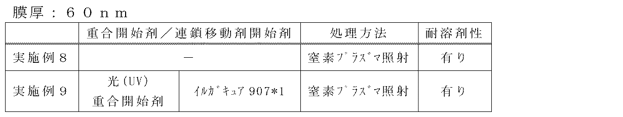
上記結果から、膜厚を変化させても、重合開始剤を添加しなくても(実施例8)、又は重合開始剤の添加量が少なくても(実施例9)、耐溶剤性に優れる、高い硬膜度を有する有機薄膜が得られたことが理解できる。
実施例8及び9のそれぞれの有機薄膜について、配向性を上記と同様に評価したところ、実施例1及び2の評価結果とそれぞれ同様であった。
実施例8及び9のそれぞれの有機薄膜について、配向性を上記と同様に評価したところ、実施例1及び2の評価結果とそれぞれ同様であった。
3.実施例10及び11、比較例4
(1)実施例10及び11
前記重合性液晶化合物(1)の代わりに、下記の重合性液晶化合物(2)を使用したこと以外は、実施例1及び2と同様にして塗布液をそれぞれ調製した。なお、下記重合性液晶化合物(2)は、スメクチック相を形成可能な液晶化合物であり、スメクチック相からネマチック相への相転移温度は129℃であった。
(1)実施例10及び11
前記重合性液晶化合物(1)の代わりに、下記の重合性液晶化合物(2)を使用したこと以外は、実施例1及び2と同様にして塗布液をそれぞれ調製した。なお、下記重合性液晶化合物(2)は、スメクチック相を形成可能な液晶化合物であり、スメクチック相からネマチック相への相転移温度は129℃であった。
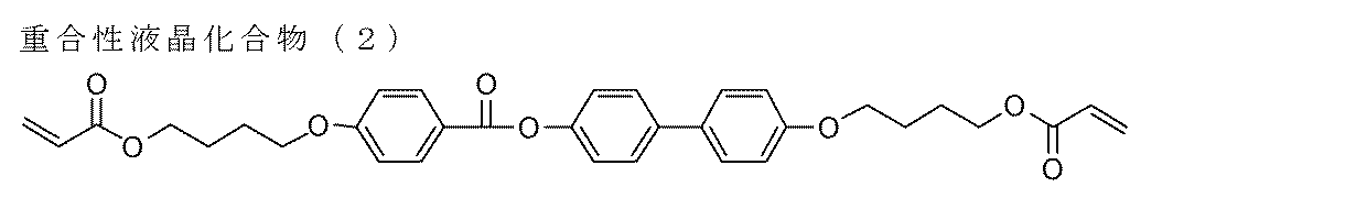
前記塗布液を、実施例1と同様にして作製した、ラビング処理された水平配向膜付きガラスのラビング処理面にそれぞれ塗布し、塗膜を形成した。
塗膜を115℃でアニール処理すると同時に、実施例1及び2と同様にして、それぞれプラズマ照射を行い、重合反応を進行させて、硬化させ、膜厚600nmの有機薄膜をそれぞれ形成した。
塗膜を115℃でアニール処理すると同時に、実施例1及び2と同様にして、それぞれプラズマ照射を行い、重合反応を進行させて、硬化させ、膜厚600nmの有機薄膜をそれぞれ形成した。
(2)比較例4
前記重合性液晶化合物(1)の代わりに、前記重合性液晶化合物(2)を用いた以外は、比較例1と同様にして、塗布液を調製し、該塗布液を用いて、比較例1と同様にして、UV光を照射して、重合反応を進行させ、硬化して、膜厚600nmの有機薄膜を形成した。
前記重合性液晶化合物(1)の代わりに、前記重合性液晶化合物(2)を用いた以外は、比較例1と同様にして、塗布液を調製し、該塗布液を用いて、比較例1と同様にして、UV光を照射して、重合反応を進行させ、硬化して、膜厚600nmの有機薄膜を形成した。
上記と同様にして、相転移温度、及び配向性評価を行った。
また、各有機薄膜について、表面の粘着性を、処理した膜表面にPETフィルム(厚さ50μm)を貼付したのち、剥離し、PETフィルム上の異物の有無を、デジタルマイクロスコープVHX-100(キーエンス社製)を用いて観察することで評価した。粘着性があることは、未硬化状態であることを意味する。
結果を下記表に示す。
また、各有機薄膜について、表面の粘着性を、処理した膜表面にPETフィルム(厚さ50μm)を貼付したのち、剥離し、PETフィルム上の異物の有無を、デジタルマイクロスコープVHX-100(キーエンス社製)を用いて観察することで評価した。粘着性があることは、未硬化状態であることを意味する。
結果を下記表に示す。

比較例4の有機薄膜は、粘着性があり重合反応が十分に進行していなかったことが理解できる。一方、実施例10及び11では、重合反応の進行が十分であり、高い硬膜度を有する有機薄膜が形成されたことが理解できる。
4.実施例12及び13、比較例5
(1)実施例12及び13
前記重合性液晶化合物(1)に代えて、下記のスメクチック液晶性有機半導体を用いた以外は、実施例1及び2と同様にして、塗布液をそれぞれ調製した。下記のスメクチック液晶性有機半導体は、スメクチック相を形成可能な液晶性有機半導体化合物である。
(1)実施例12及び13
前記重合性液晶化合物(1)に代えて、下記のスメクチック液晶性有機半導体を用いた以外は、実施例1及び2と同様にして、塗布液をそれぞれ調製した。下記のスメクチック液晶性有機半導体は、スメクチック相を形成可能な液晶性有機半導体化合物である。
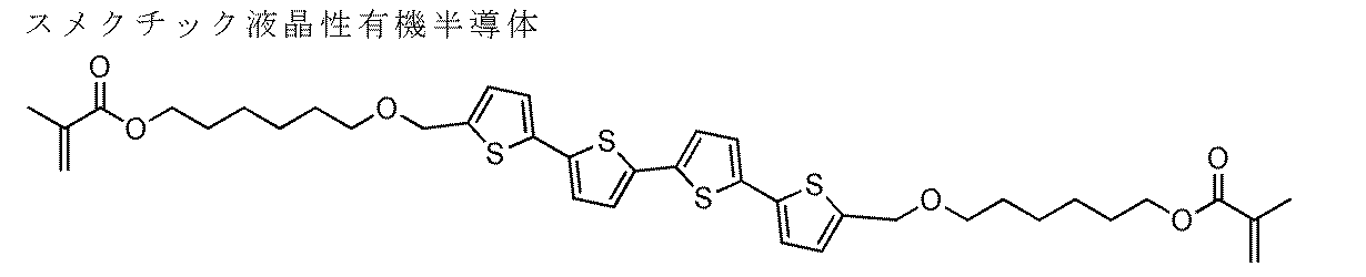
前記塗布液を、実施例1と同様にして作製した、ラビング処理された水平配向膜のラビング処理面にそれぞれ塗布し、塗膜を形成した。
塗膜を90℃でアニール処理すると同時に、実施例1及び2と同様にして、それぞれプラズマ照射を行い、重合反応を進行させて、硬化させ、膜厚100nmの有機薄膜をそれぞれ形成した。
塗膜を90℃でアニール処理すると同時に、実施例1及び2と同様にして、それぞれプラズマ照射を行い、重合反応を進行させて、硬化させ、膜厚100nmの有機薄膜をそれぞれ形成した。
(2)比較例5
前記重合性液晶化合物(1)に代えて、上記のスメクチック液晶性有機半導体を用いた以外は、比較例1と同様にして、塗布液を調製した。この塗布液を用い、アニール温度条件を90℃に変えたこと以外は、比較例1と同様にしてUV照射により重合反応を進行させて、比較例5の有機薄膜を形成した。
前記重合性液晶化合物(1)に代えて、上記のスメクチック液晶性有機半導体を用いた以外は、比較例1と同様にして、塗布液を調製した。この塗布液を用い、アニール温度条件を90℃に変えたこと以外は、比較例1と同様にしてUV照射により重合反応を進行させて、比較例5の有機薄膜を形成した。
作製した各有機薄膜について、配向性及び耐溶剤性を上記と同様にしてそれぞれ評価した。評価結果を下記表に記載する。

形成された各実施例の有機薄膜は、比較例5と異なり配向を維持したまま重合が可能であり、かつ、耐溶剤性に優れ、高い硬膜度を有する有機薄膜であることが理解できる。
前記有機薄膜は、有機トランジスタ、特にボトムゲート型の有機トランジスタ、の有機半導体層として有用である。実施例12および13の有機薄膜は、キャリアトラップの原因になる重合開始剤を含まない(実施例12)、もしくは含んでいてもわずか(実施例13)であるので、高性能が期待できる。
なお、比較例5においては、窒素雰囲気下でアニール処理中に、重合が進行し、配向することなく、硬化した。
前記有機薄膜は、有機トランジスタ、特にボトムゲート型の有機トランジスタ、の有機半導体層として有用である。実施例12および13の有機薄膜は、キャリアトラップの原因になる重合開始剤を含まない(実施例12)、もしくは含んでいてもわずか(実施例13)であるので、高性能が期待できる。
なお、比較例5においては、窒素雰囲気下でアニール処理中に、重合が進行し、配向することなく、硬化した。
5.実施例14
(有機トランジスタの作製)
図1に示す構成の電界効果型有機トランジスタを作製した。具体的には、まず、無アルカリガラス基板1上にクロムを蒸着し、ゲート電極2とした。次にスパッタ法により、2000オングストロームの酸化シリコンからなる絶縁膜3を製膜した後、クロム、金の順に蒸着を行い、通常の光リソグラフィー技術でソース電極4及びドレイン電極5を形成した。次いで、UVオゾン処理した基板上に、配向膜としてポリイミド薄膜(LX-1400、日立化成デュポンマイクロシステムズ社製)を形成し、実施例1と同様にラビング処理を行い、該配向膜の表面上に実施例12に記載と同様に、半導体活性層となる有機薄膜を作製した。
(有機トランジスタの作製)
図1に示す構成の電界効果型有機トランジスタを作製した。具体的には、まず、無アルカリガラス基板1上にクロムを蒸着し、ゲート電極2とした。次にスパッタ法により、2000オングストロームの酸化シリコンからなる絶縁膜3を製膜した後、クロム、金の順に蒸着を行い、通常の光リソグラフィー技術でソース電極4及びドレイン電極5を形成した。次いで、UVオゾン処理した基板上に、配向膜としてポリイミド薄膜(LX-1400、日立化成デュポンマイクロシステムズ社製)を形成し、実施例1と同様にラビング処理を行い、該配向膜の表面上に実施例12に記載と同様に、半導体活性層となる有機薄膜を作製した。
以上の手順で作製した、チャネル長10μm、チャネル幅1mm、半導体活性層の厚さ約0.2μmの電界効果型トランジスタの電気特性の試験を行い、ソース電極-ドレイン電極間に流れる電流が、ゲート電極にかける電圧によって変調されることを、半導体パラメータアナライザ4155C(アジレント社製)にて観測した。
6.実施例15~18、比較例6~8
(配向膜の成膜)
実施例1と同様に水平配向膜を青板ガラス上に成膜した。
(有機薄膜形成用塗布液の調製及び塗膜の形成)
(配向膜の成膜)
実施例1と同様に水平配向膜を青板ガラス上に成膜した。
(有機薄膜形成用塗布液の調製及び塗膜の形成)
前記重合性液晶化合物(1)の4質量部と、光(UV)重合開始剤:イルガキュア907の0.08質量部とを、電子工業用2-ブタノン(関東化学製)に溶解させた溶液を調製した。次に、この溶液を孔径0.2μmのシリンジフィルターを用いて濾過し、それを塗布液として用いた。
上記塗布液をスピンコート法により、前記ラビング処理された水平配向膜付きガラスのラビング処理面に塗布し、塗膜を形成した。
なお、濾過及びスピンコートについては、グローブボックス(露点-40℃、酸素濃度1000ppm以下、窒素ガス雰囲気)内で行った。
上記塗布液をスピンコート法により、前記ラビング処理された水平配向膜付きガラスのラビング処理面に塗布し、塗膜を形成した。
なお、濾過及びスピンコートについては、グローブボックス(露点-40℃、酸素濃度1000ppm以下、窒素ガス雰囲気)内で行った。
最終的に形成される有機薄膜の膜厚が、下記表に示す膜厚になるように、塗布量を調整して、上記方法により、7種(実施例15~18、比較例6~8)の塗膜を形成した。
(アニール処理)
形成した各塗膜を、大気中にて80℃のホットプレート上で1分間、アニール処理を行った。
形成した各塗膜を、大気中にて80℃のホットプレート上で1分間、アニール処理を行った。
実施例15については、下記条件のプラズマ照射のみを行い、実施例16~18については、下記条件でUV照射を行った後に、下記条件のプラズマ照射を行った。また、比較例6~8については、下記条件でUV照射のみを行った。
(UV処理)
エドモンドオプティクス社製UVキュリングチャンバー:ELC-500を用いて、大気中にてUV照射を10分間行い、硬化させた。
(プラズマ処理)
UV照射により硬膜した塗膜に、株式会社魁半導体製、S5000型大気圧低温プラズマジェット装置(放電ガス:窒素)を用いて低温N2プラズマを30秒間照射し、有機薄膜表面の重合反応を進行させて、硬化し、有機薄膜を形成した。
(UV処理)
エドモンドオプティクス社製UVキュリングチャンバー:ELC-500を用いて、大気中にてUV照射を10分間行い、硬化させた。
(プラズマ処理)
UV照射により硬膜した塗膜に、株式会社魁半導体製、S5000型大気圧低温プラズマジェット装置(放電ガス:窒素)を用いて低温N2プラズマを30秒間照射し、有機薄膜表面の重合反応を進行させて、硬化し、有機薄膜を形成した。
形成した各有機薄膜について、上記と同様にして、相転移温度を測定し、配向性評価、及び粘着性を評価した。結果を下記表に示す。

実施例15においては、ネマチック相での配向固定が観察されるものの、視野が暗くなる現象が確認された。
一方、UV照射と窒素プラズマ照射とを併用することで、有機薄膜の膜厚が、実施例15と同一の実施例18のみならず、実施例15より顕著にその膜厚が大きい実施例16及び17についても、加熱による相転移は観察されず、十分な配向固定がなされ、かつ有機薄膜表面の粘着性がなくなり、十分硬化したものと理解される。
それに対し、UV照射のみを行った比較例6~8では、重合反応が十分に進行しておらず、未重合の液晶単分子が残存しているため、加熱によって相転移し、かつ硬化不良に伴い、表面の粘着性が発生した。
一方、UV照射と窒素プラズマ照射とを併用することで、有機薄膜の膜厚が、実施例15と同一の実施例18のみならず、実施例15より顕著にその膜厚が大きい実施例16及び17についても、加熱による相転移は観察されず、十分な配向固定がなされ、かつ有機薄膜表面の粘着性がなくなり、十分硬化したものと理解される。
それに対し、UV照射のみを行った比較例6~8では、重合反応が十分に進行しておらず、未重合の液晶単分子が残存しているため、加熱によって相転移し、かつ硬化不良に伴い、表面の粘着性が発生した。
7.実施例19
<垂直配向膜上での配向固定化>
(配向膜の成膜)
UVオゾン処理を行った青板ガラス(厚さ:1.1mm)上に、垂直配向膜塗布液SE-5300(日産化学工業商品名)をスピンコート法で成膜し、温度100℃のホットプレート上で10分間、プリベーク処理を行った。次に、温度210℃のクリーンオーブン中で1時間、ポストベーク処理を行い、垂直配向膜を成膜したガラスを作製した。
<垂直配向膜上での配向固定化>
(配向膜の成膜)
UVオゾン処理を行った青板ガラス(厚さ:1.1mm)上に、垂直配向膜塗布液SE-5300(日産化学工業商品名)をスピンコート法で成膜し、温度100℃のホットプレート上で10分間、プリベーク処理を行った。次に、温度210℃のクリーンオーブン中で1時間、ポストベーク処理を行い、垂直配向膜を成膜したガラスを作製した。
前記垂直配向膜の表面に、実施例5で調製した塗布液(高分子アゾ系重合開始剤を含む塗布液)を塗布して塗膜を形成した。この塗膜を24時間大気中で保管して、塗膜の変化を目視で観察したところ、この塗膜には、結晶化は生じなかった。
この塗膜に、実施例5と同様にして、窒素プラズマ照射を行って有機薄膜を形成した。上記と同様にして、相転移温度を測定し、配向性評価及び粘着性を評価した結果を、下記表に示す。
この塗膜に、実施例5と同様にして、窒素プラズマ照射を行って有機薄膜を形成した。上記と同様にして、相転移温度を測定し、配向性評価及び粘着性を評価した結果を、下記表に示す。

上記結果から、実施例19の有機薄膜では、結晶化が抑制されており、プラズマ照射により、垂直配向膜上で形成された配向状態を維持したまま、配向固定化ができたことが理解できる。
参考例:
前記垂直配向膜の表面に、実施例1で調製した塗布液(低分子量の重合開始剤を含む塗布液)を塗布して塗膜を形成した。この塗膜についても、実施例19と同様に24時間大気中で保管して、塗膜の変化を目視で観察したところ、この塗膜では、結晶化が観察された。
前記垂直配向膜の表面に、実施例1で調製した塗布液(低分子量の重合開始剤を含む塗布液)を塗布して塗膜を形成した。この塗膜についても、実施例19と同様に24時間大気中で保管して、塗膜の変化を目視で観察したところ、この塗膜では、結晶化が観察された。
上記結果から、長時間の配向処理では、重合反応の進行が懸念されるのみならず、結晶化による配向の乱れも懸念されるが、高分子アゾ系重合開始剤を用いることで、長時間の配向処理が必要であっても、高い配向度及び高い硬膜度を両立できることが理解できる。
1 基板
2 ゲート電極
3 ゲート絶縁膜
4 ソース電極
5 ドレイン電極
6 半導体層(本発明の有機薄膜)
2 ゲート電極
3 ゲート絶縁膜
4 ソース電極
5 ドレイン電極
6 半導体層(本発明の有機薄膜)
Claims (14)
- 少なくとも1種の重合性液晶化合物を含有する組成物の配向を、プラズマ照射による重合により固定してなる有機薄膜。
- 前記組成物が、重合開始剤及び連鎖移動剤の少なくともいずれか一方を含有する請求項1に記載の有機薄膜。
- 厚さが、50~2500nmである請求項1又は2に記載の有機薄膜。
- 表面の水の接触角が、80°以下である請求項1~3のいずれか1項に記載の有機薄膜。
- 前記重合開始剤として、光重合開始剤を用いる請求項2~4のいずれか1項に記載の有機薄膜。
- 前記プラズマ照射を窒素ガスプラズマを用いて行う請求項1~5のいずれか1項に記載の有機薄膜。
- 前記重合開始剤として、高分子アゾ系重合開始剤を用いる請求項2~6のいずれか1項に記載の有機薄膜。
- 請求項1~7のいずれか1項に記載の有機薄膜を有する有機トランジスタ。
- 少なくとも1種の重合性液晶化合物を含有する組成物を配向させること、及び、
前記組成物を配向させるとともに、又は配向させた後に、前記組成物にプラズマを照射して重合を進行させて、配向を固定すること、
を含む有機薄膜の製造方法。 - 前記組成物が、重合開始剤及び連鎖移動剤の少なくともいずれか一方を含有する請求項9に記載の方法。
- 前記重合開始剤として、光重合開始剤を用いる請求項10に記載の方法。
- 前記重合開始剤として、高分子アゾ系重合開始剤を用いる請求項10又は11に記載の方法。
- 前記プラズマが、窒素ガスプラズマである請求項9~12のいずれか1項に記載の方法。
- 請求項9~13のいずれか1項に記載の方法によって有機薄膜を製造すること、及び、
前記有機薄膜の表面上に、有機溶媒を含む塗布液を塗布することにより膜を形成すること、
を少なくとも含む積層膜の製造方法。
Applications Claiming Priority (2)
| Application Number | Priority Date | Filing Date | Title |
|---|---|---|---|
| JP2011-123426 | 2011-06-01 | ||
| JP2011123426A JP5926499B2 (ja) | 2011-06-01 | 2011-06-01 | 有機薄膜、その製造方法、及びそれを有する有機トランジスタ |
Publications (1)
| Publication Number | Publication Date |
|---|---|
| WO2012165403A1 true WO2012165403A1 (ja) | 2012-12-06 |
Family
ID=47259257
Family Applications (1)
| Application Number | Title | Priority Date | Filing Date |
|---|---|---|---|
| PCT/JP2012/063702 WO2012165403A1 (ja) | 2011-06-01 | 2012-05-29 | 有機薄膜、その製造方法、及びそれを有する有機トランジスタ |
Country Status (2)
| Country | Link |
|---|---|
| JP (1) | JP5926499B2 (ja) |
| WO (1) | WO2012165403A1 (ja) |
Cited By (3)
| Publication number | Priority date | Publication date | Assignee | Title |
|---|---|---|---|---|
| JP2013010933A (ja) * | 2011-06-01 | 2013-01-17 | Fujifilm Corp | プラズマ重合膜の製造方法、画像形成方法、及びプラズマ重合膜 |
| EP3116018A4 (en) * | 2014-03-07 | 2017-03-08 | Fujifilm Corporation | Organic thin film transistor |
| JP2019215472A (ja) * | 2018-06-14 | 2019-12-19 | 住友化学株式会社 | 接着層付き積層体、積層体、液晶層積層体、液晶フィルムの製造方法、及び、光学積層体の製造方法 |
Families Citing this family (3)
| Publication number | Priority date | Publication date | Assignee | Title |
|---|---|---|---|---|
| JP2015000896A (ja) * | 2013-06-14 | 2015-01-05 | 富士フイルム株式会社 | 組成物ならびにそれを用いたミクロ相分離構造膜およびその製造方法 |
| JP6110801B2 (ja) * | 2014-03-07 | 2017-04-05 | 富士フイルム株式会社 | 有機薄膜トランジスタ |
| EP3240056B1 (en) * | 2015-03-11 | 2020-04-22 | FUJIFILM Corporation | Organic semiconductor liquid composition and method of producing organic semiconductor element using said composition |
Citations (3)
| Publication number | Priority date | Publication date | Assignee | Title |
|---|---|---|---|---|
| JPH0983040A (ja) * | 1995-09-12 | 1997-03-28 | Sharp Corp | 薄膜トランジスタ及びその製造方法 |
| JP2010501899A (ja) * | 2006-09-02 | 2010-01-21 | メルク パテント ゲゼルシャフト ミット ベシュレンクテル ハフツング | 反応性メソゲンを配向するための粒子ビーム法 |
| JP2010206197A (ja) * | 2009-03-05 | 2010-09-16 | Xerox Corp | 酸含有組成物を用いた構造部形成プロセス |
-
2011
- 2011-06-01 JP JP2011123426A patent/JP5926499B2/ja not_active Expired - Fee Related
-
2012
- 2012-05-29 WO PCT/JP2012/063702 patent/WO2012165403A1/ja active Application Filing
Patent Citations (3)
| Publication number | Priority date | Publication date | Assignee | Title |
|---|---|---|---|---|
| JPH0983040A (ja) * | 1995-09-12 | 1997-03-28 | Sharp Corp | 薄膜トランジスタ及びその製造方法 |
| JP2010501899A (ja) * | 2006-09-02 | 2010-01-21 | メルク パテント ゲゼルシャフト ミット ベシュレンクテル ハフツング | 反応性メソゲンを配向するための粒子ビーム法 |
| JP2010206197A (ja) * | 2009-03-05 | 2010-09-16 | Xerox Corp | 酸含有組成物を用いた構造部形成プロセス |
Cited By (7)
| Publication number | Priority date | Publication date | Assignee | Title |
|---|---|---|---|---|
| JP2013010933A (ja) * | 2011-06-01 | 2013-01-17 | Fujifilm Corp | プラズマ重合膜の製造方法、画像形成方法、及びプラズマ重合膜 |
| EP3116018A4 (en) * | 2014-03-07 | 2017-03-08 | Fujifilm Corporation | Organic thin film transistor |
| TWI648889B (zh) * | 2014-03-07 | 2019-01-21 | 日商富士軟片股份有限公司 | 有機薄膜電晶體 |
| JP2019215472A (ja) * | 2018-06-14 | 2019-12-19 | 住友化学株式会社 | 接着層付き積層体、積層体、液晶層積層体、液晶フィルムの製造方法、及び、光学積層体の製造方法 |
| CN110609348A (zh) * | 2018-06-14 | 2019-12-24 | 住友化学株式会社 | 带有粘接层的层叠体、层叠体、液晶层层叠体、液晶膜的制造方法、光学层叠体的制造方法 |
| JP7122168B2 (ja) | 2018-06-14 | 2022-08-19 | 住友化学株式会社 | 接着層付き積層体、積層体、液晶層積層体、液晶フィルムの製造方法、及び、光学積層体の製造方法 |
| CN110609348B (zh) * | 2018-06-14 | 2022-09-13 | 住友化学株式会社 | 带有粘接层的层叠体、层叠体、液晶层层叠体、液晶膜的制造方法、光学层叠体的制造方法 |
Also Published As
| Publication number | Publication date |
|---|---|
| JP5926499B2 (ja) | 2016-05-25 |
| JP2012253132A (ja) | 2012-12-20 |
Similar Documents
| Publication | Publication Date | Title |
|---|---|---|
| WO2012165403A1 (ja) | 有機薄膜、その製造方法、及びそれを有する有機トランジスタ | |
| CN103748506B (zh) | 液晶显示元件的制造方法、液晶取向剂以及液晶显示元件 | |
| WO2016072498A1 (ja) | 液晶表示素子 | |
| JP2020144373A (ja) | 光学異方性シート | |
| TWI778255B (zh) | 包括絕緣膜的液晶元件、調光窗及其製造方法 | |
| KR102430605B1 (ko) | 액정 배향제, 액정 배향막 및 액정 표시 소자 | |
| US20170003418A1 (en) | Compound containing mesogenic group, and mixture, composition, and optically anisotropic body using said compound | |
| JP5532974B2 (ja) | 液晶層形成用組成物、円偏光分離シート及びその製造方法、並びに輝度向上フィルム及び液晶表示装置 | |
| JP5885049B2 (ja) | 重合性液晶組成物の製造方法 | |
| CN107003571B (zh) | 液晶表示元件 | |
| JP2012194538A (ja) | 液晶配向剤、液晶配向膜及び液晶表示素子 | |
| TWI747882B (zh) | 液晶顯示元件 | |
| JP5579228B2 (ja) | プラズマ重合膜の製造方法、画像形成方法、及びプラズマ重合膜 | |
| JP4802451B2 (ja) | 重合性液晶組成物及びこれの重合物 | |
| JP2015145450A (ja) | 光応答性架橋型液晶高分子フィルムの製造方法および該製造方法により得られる光応答性架橋型液晶高分子フィルム | |
| KR20130109050A (ko) | 혼합물 및 그 제조 방법 | |
| TW201731889A (zh) | 化合物、硬化物、聚合物、聚合物溶液、光配向膜、光學異向體、及液晶顯示元件 | |
| CN108700766B (zh) | 液晶表示元件 | |
| CN111748358A (zh) | 液晶组合物及液晶显示元件 | |
| TW201629601A (zh) | 液晶顯示裝置之製造方法 | |
| JP2005272560A (ja) | 重合性液晶組成物、及びこれの重合物 | |
| JP6223214B2 (ja) | 光応答性架橋型液晶高分子フィルムの製造方法および該製造方法により得られる光応答性架橋型液晶高分子フィルム | |
| CN111679509A (zh) | 水平取向型液晶显示元件、液晶组合物、显示装置及水平取向型液晶显示元件的制造方法 | |
| Ahmad et al. | Pluronic polymer crosslinked with thiolene in polymer dispersed liquid crystal films | |
| CN110724536A (zh) | 液晶组合物、水平取向型液晶显示元件及其制造方法及显示装置 |
Legal Events
| Date | Code | Title | Description |
|---|---|---|---|
| 121 | Ep: the epo has been informed by wipo that ep was designated in this application |
Ref document number: 12792950 Country of ref document: EP Kind code of ref document: A1 |
|
| NENP | Non-entry into the national phase |
Ref country code: DE |
|
| 122 | Ep: pct application non-entry in european phase |
Ref document number: 12792950 Country of ref document: EP Kind code of ref document: A1 |