WO2012164980A1 - スイッチ付きコネクタ - Google Patents
スイッチ付きコネクタ Download PDFInfo
- Publication number
- WO2012164980A1 WO2012164980A1 PCT/JP2012/053848 JP2012053848W WO2012164980A1 WO 2012164980 A1 WO2012164980 A1 WO 2012164980A1 JP 2012053848 W JP2012053848 W JP 2012053848W WO 2012164980 A1 WO2012164980 A1 WO 2012164980A1
- Authority
- WO
- WIPO (PCT)
- Prior art keywords
- terminal
- connector
- switch
- axis direction
- plating
- Prior art date
- Legal status (The legal status is an assumption and is not a legal conclusion. Google has not performed a legal analysis and makes no representation as to the accuracy of the status listed.)
- Ceased
Links
Images



Classifications
-
- H—ELECTRICITY
- H01—ELECTRIC ELEMENTS
- H01R—ELECTRICALLY-CONDUCTIVE CONNECTIONS; STRUCTURAL ASSOCIATIONS OF A PLURALITY OF MUTUALLY-INSULATED ELECTRICAL CONNECTING ELEMENTS; COUPLING DEVICES; CURRENT COLLECTORS
- H01R13/00—Details of coupling devices of the kinds covered by groups H01R12/70 or H01R24/00 - H01R33/00
- H01R13/66—Structural association with built-in electrical component
- H01R13/70—Structural association with built-in electrical component with built-in switch
-
- H—ELECTRICITY
- H01—ELECTRIC ELEMENTS
- H01R—ELECTRICALLY-CONDUCTIVE CONNECTIONS; STRUCTURAL ASSOCIATIONS OF A PLURALITY OF MUTUALLY-INSULATED ELECTRICAL CONNECTING ELEMENTS; COUPLING DEVICES; CURRENT COLLECTORS
- H01R24/00—Two-part coupling devices, or either of their cooperating parts, characterised by their overall structure
- H01R24/38—Two-part coupling devices, or either of their cooperating parts, characterised by their overall structure having concentrically or coaxially arranged contacts
- H01R24/40—Two-part coupling devices, or either of their cooperating parts, characterised by their overall structure having concentrically or coaxially arranged contacts specially adapted for high frequency
- H01R24/42—Two-part coupling devices, or either of their cooperating parts, characterised by their overall structure having concentrically or coaxially arranged contacts specially adapted for high frequency comprising impedance matching means or electrical components, e.g. filters or switches
- H01R24/46—Two-part coupling devices, or either of their cooperating parts, characterised by their overall structure having concentrically or coaxially arranged contacts specially adapted for high frequency comprising impedance matching means or electrical components, e.g. filters or switches comprising switches
Definitions
- the present invention relates to a connector with a switch, and more particularly to a connector with a switch through which a high-frequency signal is transmitted.
- FIG. 8 is a cross-sectional structure diagram of the coaxial connector 500 described in Patent Document 1. As shown in FIG.
- the coaxial connector 500 includes a yoke terminal 502, a movable terminal 504, a yoke terminal 506, and a magnet 508, as shown in FIG.
- the yoke terminals 502 and 506 are opposed to each other with the magnet 508 interposed therebetween, and are in contact with the magnet 508. Normally, the movable terminal 504 is in contact with the yoke terminals 502 and 506 by the magnetic force of the magnet 508 as shown in FIG. Thereby, the yoke terminal 502 and the yoke terminal 506 are electrically connected.
- the movable terminal 504 is pushed downward by the probe 600 and separated from the yoke terminal 506 as shown in FIG. Thereby, the yoke terminal 502 and the yoke terminal 506 are insulated from each other.
- the contact of the yoke terminals 502 and 506 with the movable terminal 504 is subjected to a base nickel plating process and a surface gold plating process.
- a base nickel plating process By applying the surface gold plating treatment to the contact, corrosion of the contact is prevented, and the contact reliability between the yoke terminals 502 and 506 and the movable terminal 504 is improved.
- the nickel plating film is formed on the yoke terminals 502 and 506 under the gold plating film.
- the nickel plating film has high magnetic permeability when formed by an electrolytic plating method.
- the coaxial connector 500 transmits a high-frequency signal having a frequency of about 1 GHz, for example.
- a high-frequency signal current flows concentrated on the skin of the yoke terminals 502 and 506 due to the skin effect.
- the skin depth ⁇ which is the depth at which the current density attenuates to 1 / e ( ⁇ 0.37), is expressed by the following equation (1).
- ⁇ ( ⁇ f ⁇ 0 ⁇ r) -1/2 ⁇ (1)
- ⁇ conductivity
- f frequency of high-frequency signal
- ⁇ r relative permeability
- the skin depth ⁇ of gold is 2.36 ⁇ m.
- the thickness of the gold plating film is generally 1 ⁇ m or less in view of cost.
- the current of the high-frequency signal also flows through the nickel plating film below the gold plating film.
- metals having magnetism, i.e. relative permeability mu r a strong current flows high-frequency signal to the larger metal than 1, in principle as described below, it is said to intermodulation distortion.
- the skin depth ⁇ which is a region through which a high-frequency current flows, becomes small, and the current density in a portion close to the skin of the conductor becomes extremely large.
- This large current density reduces the permeability of the skin portion (relative permeability ⁇ r ).
- the skin depth ⁇ increases and the current density of the surface layer of the magnetic metal decreases.
- the magnetic metal permeability (relative permeability ⁇ r ) increases again (however, the original permeability does not exceed).
- the skin depth ⁇ decreases and the current density of the surface layer of the magnetic metal increases.
- the current density is changed by changing the skin depth ⁇
- the change of the current density is a change of the ohmic loss
- the change of the current with respect to the change of the voltage is nonlinear.
- the yoke terminals 502 and 506 are magnetically plated with nickel, and when a high frequency current flows through the coaxial connector 500, intermodulation distortion occurs.
- an object of the present invention is to provide a connector with a switch that can suppress the occurrence of intermodulation distortion.
- a connector with a switch includes a first terminal, a second terminal, and a magnet provided at a position away from the first terminal and the second terminal.
- a switch-equipped connector used for transmitting a high-frequency signal wherein at least one of the first terminal and the second terminal includes a magnetic metal, and the second terminal includes the first terminal It is characterized by being able to contact and separate from one terminal.
- FIG. 6A is a cross-sectional structure diagram in the xz plane of the connector with switch when the counterpart connector is not attached.
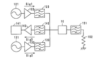
- FIG. 6B is a cross-sectional structure diagram in the xz plane of the connector with a switch when the counterpart connector is attached. It is a block diagram of the circuit which this inventor created in experiment. 2 is a cross-sectional structure diagram of a coaxial connector described in Patent Document 1.
- FIG. 1 is an external perspective view of a switch-equipped connector 10 according to an embodiment of the present invention.
- 2 and 3 are exploded perspective views of the connector 10 with a switch.
- a direction in which the external terminal 14, the upper case 16, and the lower case 18 are overlapped is a z-axis direction.
- the positive direction in the z-axis direction is a direction from the lower case 18 toward the external terminal 14.
- the direction in which the movable terminal 20 and the fixed terminal 22 are arranged is the x-axis direction
- the direction orthogonal to the x-axis direction and the z-axis direction is the y-axis direction.
- the positive direction in the x-axis direction is a direction from the movable terminal 20 toward the fixed terminal 22.
- the switch-equipped connector 10 is used for high-frequency signal transmission.
- the switch-equipped connector 10 includes a main body 12, a movable terminal 20, a fixed terminal 22, and a magnet 100, and has a size of 2 mm ⁇ 2 mm ⁇ 0.9 mm.
- the main body 12 has a metal external terminal 14 and an upper case 16 and a lower case 18 made of an insulating material, which are made of an insulating material, from the positive direction side to the negative direction side in the z-axis direction. It is configured to be stacked one after another.
- the lower case 18 has a rectangular shape and has protrusions 52a and 52b for positioning the upper case 16 on the surface on the positive side in the z-axis direction.
- the protrusions 52a and 52b extend in the x-axis direction along the sides located at both ends in the y-axis direction in the lower case 18.
- the lower case 18 is provided with holes 53a and 53b.
- rectangular cutouts for allowing the movable terminal 20 and the fixed terminal 22 to be drawn to the outside are provided at the center of each of the two sides extending in the y-axis direction of the lower case 18. Portions 54 and 55 are formed. Further, a projection 56 for positioning the movable terminal 20 is provided in the vicinity of the notch 54 in the positive direction side in the x-axis direction. A fixing surface 57 for fixing the movable terminal 20 is provided between the notch 54 and the protrusion 56. On the other hand, a fixing surface 58 for fixing the fixing terminal 22 is provided in the vicinity of the notch portion 55 on the negative side in the x-axis direction.
- the upper case 16 includes a cylindrical portion 34 and a cover portion 35 as shown in FIG.
- the cover part 35 is a plate-like member having an outer shape along the protrusions 52a and 52b, and is fitted between the protrusions 52a and 52b.
- the cylindrical portion 34 protrudes toward the positive direction side in the z-axis direction at the center of the cover portion 35.
- the cylindrical portion 34 has a mortar-shaped opening 34a on the positive side in the z-axis direction, and a hole 34a having a circular cross section on the xy plane.
- the hole 34a passes through the upper case 16.
- the probe of the mating connector is inserted into the hole 34a from the mortar-shaped opening side.
- two cylindrical ribs 36a and 36b projecting to the negative direction side in the z-axis direction are provided on the surface of the upper case 16 on the negative direction side in the z-axis direction.
- the ribs 36a and 36b are respectively inserted into holes 53a and 53b provided in the lower case 18, thereby positioning the upper case 16 and the lower case 18.
- a fixed surface 37 for fixing the movable terminal 20 is provided on the negative side surface in the z-axis direction of the upper case 16 near the end on the negative direction side in the x-axis direction. Yes.
- the fixed surface 37 fixes the movable terminal 20 together with the fixed surface 57 when the connector with switch 10 is assembled.
- a fixed surface 39 for fixing the fixed terminal 22 is provided near the end on the positive side in the x-axis direction on the surface on the negative side in the z-axis direction of the upper case 16.
- the fixed surface 39 fixes the fixed terminal 22 together with the fixed surface 58 when the connector with switch 10 is assembled.
- a mounting portion 38 is provided on the negative side of the fixed surface 39 in the x-axis direction.
- the mounting portion 38 is provided on the surface of the upper case 16 on the negative direction side in the z-axis direction so as to protrude toward the negative direction side in the z-axis direction. 50a and 50b are placed.
- FIG. 4 is an external perspective view of the state in which the movable terminal 20 and the fixed terminal 22 are mounted on the lower case 18.
- FIG. 5 is an external perspective view of the state in which the movable terminal 20 and the fixed terminal 22 are mounted on the upper case 16.
- the fixed terminal 22 is attached on the surface on the positive side of the z-axis direction of the lower case 18 as shown in FIGS.
- the fixed terminal 22 is formed by punching and bending a phosphor bronze (for example, C5191R-1 / 2H) metal plate, and the surface thereof is plated with Ni and Au. That is, Ni plating is performed on the surface of the main body of the fixed terminal 22 made of metal (phosphor bronze) by electrolytic plating, and Au plating is applied on the Ni plating.
- the thickness of the Ni plating is 0.20 ⁇ m or more and 1.00 ⁇ m or less.
- the thickness of the Au plating is 0.030 ⁇ m or more and 0.20 ⁇ m or less. In mass production, it is preferable to supply the fixed terminal 22 in a form continuously provided on the hoop material in view of cost. Since the hoop material is generally plated by an electrolytic plating method, Ni plating is usually magnetic. Tinged with
- the fixed terminal 22 includes a fixed portion 48, a lead portion 49, and contact portions 50a and 50b as shown in FIGS.
- the fixing portion 48 is a flat portion that is fixed to the main body 12 by being sandwiched between the fixing surface 39 and the fixing surface 58 when the connector with switch 10 is assembled.
- the lead portion 49 is formed by bending a portion on the positive side in the x-axis direction with respect to the fixed portion 48 of the fixed terminal 22 into an L-shape. As shown in FIGS. When 10 is assembled, it is exposed from the notch 55 to the outside of the main body 12. As shown in FIGS.
- the contact portions 50 a and 50 b are formed by bending the negative end side of the fixed terminal 22 in the x-axis direction toward the positive direction side in the z-axis direction. It contacts the movable terminal 20 at a portion facing the direction side.
- Two contact portions 50a and 50b are provided so as to correspond to branch portions 44a and 44b described later. Further, the broken line between the contact portions 50a, 50b and the fixed portion 48 is parallel to the x-axis direction.
- the fixing portion 48 between the contact portions 50 a and 50 b and the contact portions 50 a and 50 b are placed on a placement portion 38 having a shape along the contact portions 50 a and 50 b and the fixing portion 48. .
- the movable terminal 20 is attached on the surface of the lower case 18 on the positive side in the z-axis direction, as shown in FIGS.
- the movable terminal 20 is formed by punching and bending a metal plate of austenitic spring stainless steel (for example, SUS301-CSP or SUS304-CSP) having spring properties, and Ni plating and Au plating are formed on the surface. It has been subjected. That is, Ni plating is performed on the surface of the movable terminal 20 main body made of metal (austenitic stainless steel) by an electrolytic plating method, and Au plating is applied on the Ni plating.
- the thickness of the Ni plating is 0.20 ⁇ m or more and 1.00 ⁇ m or less.
- the thickness of the Au plating is 0.030 ⁇ m or more and 0.20 ⁇ m or less.
- the movable terminal 20 is made of austenitic stainless steel, the martensitic transformation is caused and the magnetism is borne.
- the movable terminal 20 is preferably supplied in a form continuously provided on the hoop material in view of cost.
- the hoop material is generally plated by an electrolytic plating method, and Ni plating is usually magnetic. Tinged with
- the movable terminal 20 includes a fixed portion 42, a lead portion 43, and a leaf spring portion 44, as shown in FIGS.
- the fixing portion 42 is a flat portion that is fixed to the main body 12 by being sandwiched between the fixing surface 37 and the fixing surface 57 when the connector with switch 10 is assembled.
- the lead portion 43 is formed by bending a portion on the negative direction side in the x-axis direction with respect to the fixed portion 42 of the movable terminal 20 into an L-shape. As shown in FIGS. When 10 is assembled, it is exposed from the notch 54 to the outside of the main body 12.
- the leaf spring portion 44 extends linearly in the x-axis direction from the fixed portion 42 toward the fixed terminal 22, and is in contact with the contact portions 50 a and 50 b of the fixed terminal 22.
- the tips ta and tb are slidably in contact with the lower case 18. More specifically, the leaf spring portion 44 has branch portions 44a and 44b that are formed by branching into two on the tip end ta and tb side (the positive direction side in the x-axis direction).
- the fixing portion 48 is located between the branch portions 44a and 44b, and the contact portions 50a and 50b of the fixed terminal 22 are respectively in the z-axis direction so as to overlap the branch portions 44a and 44b when viewed in plan from the z-axis direction. As it goes in the positive direction, it spreads in the y-axis direction. Moreover, the leaf
- a hole 45 is formed across the leaf spring portion 44 and the fixed portion 42. As shown in FIG. 4, a protrusion 56 is inserted into the hole 45. Thereby, the movable terminal 20 is positioned in the xy plane.
- the movable terminal 20 and the fixed terminal 22 configured as described above are first attached to the upper case 16 and then the movable terminal 20 is attached to the upper case 16.
- the portions on the positive direction side in the z-axis direction of the branch portions 44a and 44b and the portions on the negative direction side in the z-axis direction of the contact portions 50a and 50b come into contact.
- the external terminal 14 is formed by punching, bending, drawing, or the like from a metal plate made of brass or beryllium copper, and the surface thereof is plated with Au.
- the external terminal 14 is in contact with the outer conductor of the mating connector and includes a flat portion 31, a cylindrical portion 32, and leg portions 33a and 33b as shown in FIGS.
- the flat part 31 is a plate-like member and covers the upper case 16 from the positive direction side in the z-axis direction.
- Legs 33a and 33b are provided on the sides of the flat portion 31 located at both ends in the y-axis direction.
- the leg portions 33a and 33b are formed by bending a part of a plate-like body extending in the y-axis direction from the flat portion 31, and are fixed by sandwiching the upper case 16 and the lower case 18 as shown in FIG. To do.
- a cylindrical portion 32 that protrudes toward the positive side in the z-axis direction is provided at the center of the flat portion 31.
- the cylindrical portion 32 is formed so as to be concentric with the cylindrical portion 34 and is fitted to the outer conductor of the mating connector.
- the external terminal 14 normally functions as a ground.
- the magnet 100 is provided at a position away from the fixed terminal 22 and the movable terminal 20, and is specifically attached to the surface of the lower case 18 on the negative direction side in the z-axis direction. In the present embodiment, the magnet 100 overlaps the movable terminal 20 when viewed in plan from the z-axis direction.
- the switch-equipped connector 10 configured as described above is assembled as follows. As shown in FIG. 5, the fixed terminal 22 is aligned and attached to the upper case 16, and then the movable terminal 20 is aligned and attached to the upper case 16.
- the external terminal 14 is attached to the upper case 16 from the positive direction side in the z-axis direction.
- the cylindrical portion 34 is inserted into the cylindrical portion 32.
- the leg portions 33a and 33b are bent, but actually, the leg portions 33a and 33b are not bent at this stage.
- the lower case 18 is stacked on the upper case 16 from the negative direction side in the z-axis direction.
- the ribs 36a and 36b are inserted into the holes 53a and 53b.
- the magnet 100 is attached to the surface on the negative side in the z-axis direction of the lower case 18 with an adhesive or the like. Thereby, the connector 10 with a switch which has a structure as shown in FIG. 1 can be obtained.
- FIG. 6A is a cross-sectional structure diagram in the xz plane of the switch-equipped connector 10 when the counterpart connector is not attached.
- FIG. 6B is a cross-sectional structure diagram in the xz plane of the switch-equipped connector 10 when the counterpart connector is attached.
- the movable terminal 20 when the counterpart connector is not attached, the movable terminal 20 is in a state where the central portion in the x-axis direction swells in the positive direction side in the z-axis direction. Accordingly, the branch portions 44a and 44b (only the branch portion 44a is shown in FIG. 6) are pressed against the contact portions 50a and 50b (only the contact portion 50a is shown in FIG. 6) by the urging force of the leaf spring portion 44.
- the movable terminal 20 and the fixed terminal 22 are electrically connected.
- the probe 130 of the mating connector is inserted from the positive direction side in the z-axis direction to the negative direction side through the hole 34a.
- the probe 130 contacts the leaf spring portion 44 and pushes down the leaf spring portion 44 toward the negative direction side in the z-axis direction. That is, the leaf spring portion 44 is displaced in a direction away from the fixed terminal 22 by the probe 130.
- the branch portions 44a and 44b of the leaf spring portion 44 are separated from the contact portions 50a and 50b, and the electrical connection between the movable terminal 20 and the fixed terminal 22 is cut off.
- the probe 130 and the movable terminal 20 are electrically connected.
- the outer conductor (not shown) of the mating connector is fitted to the external terminal 14, and the outer conductor is also electrically connected to the external terminal 14.
- the switch-equipped connector 10 configured as described above can suppress the occurrence of corrosion at the contact point of the movable terminal 20 with the fixed terminal 22. More specifically, the surface of the movable terminal 20 of the connector with switch 10 is plated with gold having excellent environmental resistance. Therefore, the contact between the movable terminal 20 and the fixed terminal 22 is protected by gold. As a result, the occurrence of corrosion at the contact point of the movable terminal 20 with the fixed terminal 22 is suppressed.
- the connector with switch 10 can suppress the occurrence of intermodulation distortion. More specifically, in the coaxial connector 500 described in Patent Document 1, the yoke terminals 502 and 506 are formed with a nickel plating film under the gold plating film. The nickel plating film has high magnetic permeability when formed by an electrolytic plating method. As a result, intermodulation distortion occurs in the coaxial connector 500.
- the switch-equipped connector 10 is provided with a magnet 100.
- the magnet 100 generates magnetic saturation in the movable terminal 20 main body and Ni plating. That is, the relative magnetic permeability ⁇ r of the movable terminal 20 main body and the Ni plating approaches 1. As a result, the occurrence of intermodulation distortion in the connector with switch 100 is suppressed.
- the connector with switch 10 can suppress the occurrence of intermodulation distortion for the following reason. More specifically, when a high frequency signal flows through the fixed terminal 22 and the movable terminal 20, an electromagnetic field is generated around the fixed terminal 22 and the movable terminal 20.
- the magnet 100 is generally made of ferrite or the like, and is a magnetic body and a dielectric body. When the magnet 100 is in contact with the fixed terminal 22 and the movable terminal 20 through which an actual current flows, there is a high possibility of causing non-linearity in the change in current with respect to voltage.
- the magnet 100 when the magnet 100 is in contact with the fixed terminal 22 or the movable terminal 20, most of the magnetic field generated by the current enters the magnet, and the magnet The distorted magnetic field affects the current again, causing non-linearity in the change of the current with respect to the voltage, and intermodulation distortion occurs. Therefore, in the connector with switch 10, the magnet 100 is provided at a position away from the fixed terminal 22 and the movable terminal 20. As a result, the amount of the magnetic field generated by the high-frequency current entering the magnet 100 is reduced, and the amount that the distortion of the magnetic field affects the current again is significantly reduced. As a result, the intermodulation distortion is suppressed in the connector with switch 10.
- the distance between the magnet 100 and the fixed terminal 22 or the movable terminal 20 is a design matter required by experiments and the like in consideration of the size, material, strength, and magnitude of power flowing through the connector.
- the connector 10 with a switch the occurrence of corrosion in the movable terminal 20 body made of austenitic stainless steel is suppressed.
- the thinly formed Au plating is a porous film, and the ionization tendency of Au is the most noble. Therefore, when the Au plating is directly formed on the movable terminal 20 main body, the stainless steel, which is the base metal of the Au plating, is exposed from the Au plating hole. When moisture in the air adheres to the exposed stainless steel, a galvanic cell effect occurs between the stainless steel and the Au plating, and a current flows between the stainless steel and the Au plating. As a result, corrosion occurs in the stainless steel. Therefore, in the connector with switch 10, Ni plating is provided on the base of Au plating. Ni plating is less likely to corrode than stainless steel. Therefore, in the connector with switch 10, the occurrence of corrosion on the movable terminal 20 body is suppressed.
- Ni plating is formed by the electrolytic plating method, it is magnetic.
- Ni plating formed by an electroless plating method and containing 5% or more of P (phosphorus) is not magnetic. Therefore, it is conceivable to form Ni plating by the electroless plating method in the connector with switch 10 as well.
- the movable terminal 20 is manufactured by performing a punching process and a bending process on a band-shaped hoop material, and then performing plating in a state connected to the hoop material. And the movable terminal 20 is cut
- the reason why electroless plating is not generally performed in the continuous plating of the hoop material is as follows. 1) It is difficult to obtain a plating having excellent adhesion. 2) The number of steps is large and the operation is complicated. 3) Since the length of processing time in each process is different, it is difficult to carry out continuously.
- austenitic stainless steel for springs is used as the material of the movable terminal 20 main body.
- austenitic stainless steel has a property that it undergoes martensitic transformation by bending and becomes magnetic. Therefore, it is conceivable to use phosphor bronze as the material of the movable terminal 20 main body in the same manner as the material of the movable terminal 20 main body. Phosphor bronze is not magnetized by bending.
- phosphor bronze generally has a smaller spring constant than austenitic stainless steel for springs, and the pressure contact force between the movable terminal 20 and the fixed terminal 22 is small.
- austenitic spring stainless steel having a large spring constant as the material of the movable terminal 20 body.
- FIG. 7 is a block diagram of a circuit created by the inventor in an experiment.
- a connector 10 with a switch includes a connector 10 with a switch, signal generators 121 and 131, power amplifiers 122 and 132, an amplifier 142, bandpass filters 123, 133, 143, and 151, a spectrum analyzer 141, and a dummy load 152.
- the signal generator 121 generates a high frequency signal Sig1 having a frequency F1.
- the power amplifier 122 amplifies the high frequency signal Sig1.
- the bandpass filter 123 has a pass band that allows the high-frequency signal Sig1 to pass through, and has an attenuation region that attenuates a high-frequency signal Sig2 and an intermodulation distortion Sig3, which will be described later, by a predetermined amount or more.
- the signal generator 131 generates a high frequency signal Sig2 having a frequency F2 (> F1).
- the power amplifier 132 amplifies the high frequency signal Sig2.
- the band-pass filter 133 has a pass band that allows the high-frequency signal Sig2 to pass therethrough, and has an attenuation region that attenuates the high-frequency signal Sig1 and intermodulation distortion Sig3 described later by a predetermined amount or more.
- the band-pass filter 143 has a pass band that allows passage of intermodulation distortion Sig3, which will be described later, and has an attenuation band that attenuates the high-frequency signals Sig1 and Sig2 by a predetermined amount or more.
- the amplifier 142 amplifies the output from the band pass filter 143 and outputs it to the spectrum analyzer 141.
- the high-frequency signals Sig 1 and Sig 2 that have passed through the switch-equipped connector 10 pass through the band-pass filter 151 and are consumed by the dummy load 152.
- the band pass filter 151 prevents the intermodulation distortion generated in the dummy load 152 from flowing back to the connector 10 with switch and being input to the amplifier 142.
- intermodulation distortion Sig3 having the frequency FIM is generated in the connector with switch 10.
- the frequency FIM is 2F1-F2 or 2F2-F1.
- the frequency FIM is 3F1-2F2 or 3F2-2F1. Further higher order intermodulation distortion is also generated.
- the intermodulation distortion Sig3 passes through the bandpass filter 143, is amplified by the amplifier 142, and is input to the spectrum analyzer 141.
- the inventor of the present application examined the intensity of the third-order intermodulation distortion Sig3 generated in the connector 10 with the switch by using the spectrum analyzer 141. In addition, as a comparison object, the inventor of the present application also examined the strength of the intermodulation distortion Sig3 generated in the connector with a switch not provided with the magnet 100 by the same method.
- the strength of the intermodulation distortion Sig3 was ⁇ 103 dB to ⁇ 105 dB in the connector with a switch not provided with the magnet 100.
- the intensity of the intermodulation distortion Sig3 was ⁇ 118 dB (below the measurement limit). Therefore, it can be seen that the provision of the magnet 100 suppresses intermodulation distortion.
- the present invention is useful for a connector with a switch, and is particularly excellent in that the occurrence of intermodulation distortion can be suppressed.
Landscapes
- Details Of Connecting Devices For Male And Female Coupling (AREA)
- Coupling Device And Connection With Printed Circuit (AREA)
Abstract
相互変調歪みが発生することを抑制できるスイッチ付きコネクタを提供することである。 固定端子(22)は、下ケース(18)のz軸方向の正方向側の面上に取り付けられている。可動端子(20)は、オーステナイト系ステンレスにNiめっき及びAuめっきが施されてなり、固定端子(22)に対して接離可能に圧接している。磁石(100)は、下ケース(18)のz軸方向の負方向側の面上に取り付けられており、固定端子(22)及び可動端子(20)から離れた位置に設けられている。
Description
本発明は、スイッチ付きコネクタに関し、より特定的には、高周波信号が伝送されるスイッチ付きコネクタに関する。
従来のスイッチ付きコネクタとしては、例えば、特許文献1に記載の同軸コネクタが知られている。図8は、特許文献1に記載の同軸コネクタ500の断面構造図である。
同軸コネクタ500は、図8に示すように、ヨーク端子502、可動端子504、ヨーク端子506及び磁石508を備えている。
ヨーク端子502,506は、磁石508を挟んで対向しており、磁石508に接触している。可動端子504は、通常では、図8(a)に示すように、磁石508の磁力により、ヨーク端子502,506に接触している。これにより、ヨーク端子502とヨーク端子506との間が導通している。
一方、可動端子504は、プローブ600が挿入されると、図8(b)に示すように、プローブ600により下方に押し下げられて、ヨーク端子506から離れる。これにより、ヨーク端子502とヨーク端子506との間が絶縁される。
以上の同軸コネクタ500では、ヨーク端子502,506における可動端子504との接点には、下地ニッケルメッキ処理及び表面金メッキ処理が施されている。表面金メッキ処理が接点に施されることにより、接点の腐食が防止され、ヨーク端子502,506と可動端子504との接触信頼性が向上する。
しかしながら、特許文献1に記載の同軸コネクタ500では、以下に説明するように、相互変調歪みが発生する可能性が高い。前記の通り、ヨーク端子502,506には、金メッキ膜の下にはニッケルメッキ膜が形成されている。ニッケルメッキ膜は、電解メッキ法により形成されると、高い透磁率を有する。
ここで、同軸コネクタ500では、例えば、1GHz程度の周波数を有する高周波信号が伝送される。このような高周波信号の電流は、表皮効果により、ヨーク端子502,506の表皮に集中して流れる。そして、電流密度が1/e(≒0.37)に減衰する深さである表皮深さδは、以下の式(1)に示される。
δ=(πfσμ0μr)-1/2・・・(1)
σ:導電率
f:高周波信号の周波数
μ0:真空の透磁率(=4π×10-7)
μr:比透磁率
σ:導電率
f:高周波信号の周波数
μ0:真空の透磁率(=4π×10-7)
μr:比透磁率
高周波信号の周波数fを1GHzとすると、式(1)によれば、金の表皮深さδは2.36μmとなる。一方、金メッキ膜の厚さは、コストを鑑みて一般的に、1μm以下である。そのため、高周波信号の電流は、金メッキ膜の下層のニッケルメッキ膜にも流れる。一般に磁性を有する金属、即ち比透磁率μrが1より大きな金属に高周波信号の強い電流が流れると、以下に説明するような原理で、相互変調歪みが発生すると言われている。
高い透磁率を有する磁性金属では、高周波電流が流れる領域である表皮深さδが小さくなり、導体の表皮に近い部分の電流密度が著しく大きくなる。そしてこの大きな電流密度により表皮部分の透磁率(比透磁率μr)が減少する。透磁率(比透磁率μr)が減少すると、表皮深さδは大きくなり、磁性金属の表層の電流密度が減少する。
一方、表層の電流密度が減少すると、磁性金属の透磁率(比透磁率μr)は再び増加する(但し元の透磁率は越えない)。透磁率(比透磁率μr)が増加すると、表皮深さδは小さくなり、磁性金属の表層の電流密度が増加する。
以上のように、表皮深さδが変化することにより電流密度が変化し、電流密度の変化はオーミック損の変化となり、電圧の変化に対する電流の変化が非線形になる。ヨーク端子502,506には磁性を有するニッケルメッキが施されており、同軸コネクタ500に大きな高周波電流が流れたとき、相互変調歪みが発生する。
そこで、本発明の目的は、相互変調歪みが発生することを抑制できるスイッチ付きコネクタを提供することである。
本発明の一形態に係るスイッチ付きコネクタは、第1の端子と、第2の端子と、該第1の端子及び該第2の端子から離れた位置に設けられている磁石と、を備えており、高周波信号の伝送に用いられるスイッチ付きコネクタであって、前記第1の端子と前記第2の端子の少なくとも一方は、磁性体金属を有しており、前記第2の端子は、前記第1の端子に対して接離可能であること、を特徴とする。
本発明によれば、端子の接点に腐食が発生することを抑制できると共に、相互変調歪みが発生することを抑制できる。
以下に、本発明の一実施形態に係るスイッチ付きコネクタについて、図面を参照して説明する。
(スイッチ付きコネクタの構成)
図1は、本発明の一実施形態に係るスイッチ付きコネクタ10の外観斜視図である。また、図2及び図3は、スイッチ付きコネクタ10の分解斜視図である。以下、このスイッチ付きコネクタ10の詳細について説明する。図1ないし図3において、外部端子14、上ケース16及び下ケース18が重ねられる方向をz軸方向とする。z軸方向の正方向は、下ケース18から外部端子14へと向かう方向である。また、可動端子20及び固定端子22が並ぶ方向をx軸方向とし、x軸方向とz軸方向に直交する方向をy軸方向とする。x軸方向の正方向は、可動端子20から固定端子22へと向かう方向である。
図1は、本発明の一実施形態に係るスイッチ付きコネクタ10の外観斜視図である。また、図2及び図3は、スイッチ付きコネクタ10の分解斜視図である。以下、このスイッチ付きコネクタ10の詳細について説明する。図1ないし図3において、外部端子14、上ケース16及び下ケース18が重ねられる方向をz軸方向とする。z軸方向の正方向は、下ケース18から外部端子14へと向かう方向である。また、可動端子20及び固定端子22が並ぶ方向をx軸方向とし、x軸方向とz軸方向に直交する方向をy軸方向とする。x軸方向の正方向は、可動端子20から固定端子22へと向かう方向である。
スイッチ付きコネクタ10は、高周波信号の伝送に用いられる。スイッチ付きコネクタ10は、図1に示すように、本体12、可動端子20、固定端子22及び磁石100を備え、2mm×2mm×0.9mmの大きさを有している。また、本体12は、図2に示すように、金属製の外部端子14、絶縁性材料である樹脂製の上ケース16及び下ケース18がz軸方向の正方向側から負方向側へとこの順に重ねられて構成されている。
下ケース18は、図2に示すように、矩形状をなしており、z軸方向の正方向側の面に上ケース16を位置決めするための突起52a,52bを有している。突起52a,52bは、下ケース18においてy軸方向の両端に位置する辺に沿ってx軸方向に延在している。また、下ケース18には、孔53a,53bが設けられている。
更に、図2に示すように、下ケース18のy軸方向に延在している2辺のそれぞれの中央部には、可動端子20及び固定端子22が外部に引き出されるための矩形の切り欠き部54,55が形成されている。また、切り欠き部54のx軸方向の正方向側近傍には、可動端子20を位置決めするための突起56が設けられている。該切り欠き部54と突起56との間には、可動端子20を固定するための固定面57が設けられている。一方、切り欠き部55のx軸方向の負方向側の近傍には、固定端子22を固定するための固定面58が設けられている。
上ケース16は、図2に示すように、円筒部34及びカバー部35を備えている。カバー部35は、突起52a,52bに沿った外形を有した板状部材であり、突起52a,52bの間に嵌め込まれる。円筒部34は、カバー部35の中央においてz軸方向の正方向側へと突出している。円筒部34は、z軸方向の正方向側がすり鉢状に開口し、かつ、xy平面での断面が円形の穴34aを有している。この穴34aは上ケース16を貫通している。穴34aには、相手方コネクタのプローブがすり鉢状開口側から挿入されることになる。
更に、上ケース16のz軸方向の負方向側の面には、図3に示すように、z軸方向の負方向側に突出する2つの円柱形のリブ36a,36bが設けられている。該リブ36a,36bはそれぞれ、下ケース18に設けられている孔53a,53bに挿入されることにより、上ケース16と下ケース18とを位置決めする。
また、図3に示すように、上ケース16のz軸方向の負方向側の面において、x軸方向の負方向側の端近傍に可動端子20を固定するための固定面37が設けられている。固定面37は、スイッチ付きコネクタ10が組み立てられたときに、固定面57と共に可動端子20を挟んで固定する。同様に、上ケース16のz軸方向の負方向側の面において、x軸方向の正方向側の端近傍に固定端子22を固定するための固定面39が設けられている。固定面39は、スイッチ付きコネクタ10が組み立てられたときに、固定面58と共に固定端子22を挟んで固定する。更に、固定面39のx軸方向の負方向側には、載置部38が設けられている。載置部38は、上ケース16のz軸方向の負方向側の面において、z軸方向の負方向側に突出するように設けられており、後述する固定端子22の固定部48及び接触部50a,50bが載置される。
次に、可動端子20及び固定端子22について、図1ないし図5を参照しながら説明する。図4は、下ケース18上に可動端子20及び固定端子22が取り付けられた状態の外観斜視図である。また、図5は、上ケース16上に可動端子20及び固定端子22が取り付けられた状態の外観斜視図である。
固定端子22は、図2ないし図4に示すように、下ケース18のz軸方向の正方向側の面上に取り付けられている。固定端子22は、リン青銅(例えば、C5191R-1/2H)の金属板を打ち抜き加工及び曲げ加工して形成されており、表面にNiめっき及びAuめっきが施されている。すなわち、金属(リン青銅)からなる固定端子22本体の表面に、電解めっき法によりNiめっきが施され、Niめっき上にAuめっきが施されている。Niめっきの膜厚は、0.20μm以上1.00μm以下である。Auめっきの膜厚は、0.030μm以上0.20μm以下である。量産において固定端子22はコストを鑑みればフープ材に連続的に設けられた形として供給するのが好適である、フープ材は一般的には電解めっき法によるめっきとなるため、Niめっきは通常磁性を帯びている。
固定端子22は、図2及び図3に示すように、固定部48、リード部49及び接触部50a,50bにより構成されている。固定部48は、スイッチ付きコネクタ10が組み立てられたときに、固定面39と固定面58との間に挟まれることにより本体12に固定される平坦部分である。リード部49は、固定端子22の固定部48よりもx軸方向の正方向側の部分をL字状に曲げ加工して形成されており、図1及び図4に示すように、スイッチ付きコネクタ10が組み立てられたときに、切り欠き部55から本体12の外部に露出している。接触部50a,50bは、図4及び図5に示すように、固定端子22のx軸方向の負方向側の端部をz軸方向の正方向側に折り曲げて形成され、z軸方向の負方向側を向く部分において可動端子20と接触する。該接触部50a,50bは、後述する枝部44a,44bに対応するように2つ設けられている。また、該接触部50a,50bと固定部48との間の折れ線は、x軸方向と平行である。接触部50a,50b間の固定部48及び接触部50a,50bは、図5に示すように、接触部50a,50b及び固定部48に沿った形状を有する載置部38上に載置される。
可動端子20は、図2ないし図4に示すように、下ケース18のz軸方向の正方向側の面上に取り付けられている。可動端子20は、ばね性を有するオーステナイト系のバネ用ステンレス(例えば、SUS301-CSP又はSUS304-CSP)の金属板を打ち抜き加工及び曲げ加工して形成されており、表面にNiめっき及びAuめっきが施されている。すなわち、金属(オーステナイト系ステンレス)からなる可動端子20本体の表面に、電解めっき法によりNiめっきが施され、Niめっき上にAuめっきが施されている。Niめっきの膜厚は、0.20μm以上1.00μm以下である。Auめっきの膜厚は、0.030μm以上0.20μm以下である。また、可動端子20本体は、オーステナイト系ステンレスが曲げ加工されているので、マルテンサイト変態を生じて磁性を帯びている。また、量産において可動端子20もコストを鑑みればフープ材に連続的に設けられた形として供給するのが好適である、フープ材は一般的には電解めっき法によるめっきとなり、Niめっきは通常磁性を帯びている。
可動端子20は、図2及び図3に示すように、固定部42、リード部43及び板ばね部44を備えている。固定部42は、スイッチ付きコネクタ10が組み立てられたときに、固定面37と固定面57との間に挟まれることにより本体12に固定される平坦部分である。リード部43は、可動端子20の固定部42よりもx軸方向の負方向側の部分をL字状に曲げ加工して形成されており、図1及び図4に示すように、スイッチ付きコネクタ10が組み立てられたときに、切り欠き部54から本体12の外部に露出している。
板ばね部44は、図4に示すように、固定部42から固定端子22に向かってx軸方向に直線状に延在しており、固定端子22の接触部50a,50bと接触していると共に、その先端ta,tbにおいて下ケース18に摺動可能に接触している。より詳細には、板ばね部44は、先端ta,tb側(x軸方向の正方向側)において2つに枝分かれして形成されている枝部44a,44bを有している。固定部48は、該枝部44a,44bの間に位置し、固定端子22の接触部50a,50bはそれぞれ、z軸方向から平面視したときに枝部44a,44bに重なるようにz軸方向正方向にいくにしたがってy軸方向に広がっている。また、板ばね部44は、z軸方向の正方向側に突出するように湾曲している。そのため、枝部44a,44bはそれぞれ、接触部50a,50bに板ばね部44の付勢力により圧接している。これにより、可動端子20と固定端子22は、接離可能に圧接しており、互いに電気的に接続されている。
更に、板ばね部44及び固定部42に跨って、孔45が形成されている。該孔45には、図4に示すように、突起56が挿入される。これにより、可動端子20が、xy平面内において位置決めされている。
以上のように構成された可動端子20及び固定端子22は、図5に示すように、まず、固定端子22が上ケース16に取り付けられてから、可動端子20が上ケース16に取り付けられる。これにより、枝部44a,44bのz軸方向の正方向側の部分と接触部50a,50bのz軸方向の負方向側の部分とが接触する。
外部端子14は、真鍮やベリリウム銅の金属板を打ち抜き加工、曲げ加工、絞り加工等により形成され、表面にAuめっきが施されている。外部端子14は、相手方コネクタの外導体と接触し、図1及び図2に示すように、フラット部31、円筒部32及び脚部33a,33bを備えている。
フラット部31は、板状部材であり、上ケース16をz軸方向の正方向側から覆う。フラット部31のy軸方向の両端に位置する辺には、脚部33a,33bが設けられている。脚部33a,33bは、フラット部31からy軸方向に延在する板状体の一部を折り曲げて形成されており、図1に示すように、上ケース16及び下ケース18を挟み込んで固定する。更に、フラット部31の中央部には、z軸方向の正方向側に突出する円筒部32が設けられている。円筒部32は、円筒部34と同心となるように形成されており、相手方コネクタの外導体と嵌合する。外部端子14は通常アースとして機能している。
磁石100は、固定端子22及び可動端子20から離れた位置に設けられており、具体的には、下ケース18のz軸方向の負方向側の面上に取り付けられている。本実施形態では、磁石100は、z軸方向から平面視したときに、可動端子20と重なっている。
以上のように構成されたスイッチ付きコネクタ10は、以下のように組み立てられる。図5に示すように、固定端子22を位置合わせして上ケース16に取り付け、その後、可動端子20を位置合わせして上ケース16に取り付ける。
次に、図5に示すように、上ケース16に対してz軸方向の正方向側から外部端子14を取り付ける。この際、円筒部34は、円筒部32に挿入される。なお、図5では、脚部33a,33bは、折り曲げられているが、実際には、この段階において、脚部33a,33bは、折り曲げられていない。この後、図3に示すように、上ケース16に対してz軸方向の負方向側から下ケース18を積み重ねる。この際、リブ36a,36bが、孔53a,53bに挿入される。
次に、外部端子14の脚部33a,33bをカシメる。
最後に、接着剤等により、磁石100を下ケース18のz軸方向の負方向側の面に取り付ける。これにより、図1に示すような構造を有するスイッチ付きコネクタ10を得ることができる。
(スイッチ付きコネクタの動作)
次に、スイッチ付きコネクタ10の動作について図6を参照して説明する。図6(a)は、相手方コネクタが装着されていないときのスイッチ付きコネクタ10のxz平面における断面構造図である。図6(b)は、相手方コネクタが装着されているときのスイッチ付きコネクタ10のxz平面における断面構造図である。
次に、スイッチ付きコネクタ10の動作について図6を参照して説明する。図6(a)は、相手方コネクタが装着されていないときのスイッチ付きコネクタ10のxz平面における断面構造図である。図6(b)は、相手方コネクタが装着されているときのスイッチ付きコネクタ10のxz平面における断面構造図である。
図6(a)に示すように、相手方コネクタが装着されていないとき、可動端子20は、x軸方向の中央部がz軸方向の正方向側に膨らんだ状態である。これにより、枝部44a,44b(図6では枝部44aのみ記載)は、接触部50a,50b(図6では、接触部50aのみ記載)に、板ばね部44の付勢力により圧接しており、可動端子20と固定端子22とは、電気的に接続されている。
一方、相手方コネクタが装着されるときには、穴34aを介して相手方コネクタのプローブ130が、z軸方向の正方向側から負方向側へと挿入される。これにより、プローブ130は、板ばね部44に接触し、該板ばね部44をz軸方向の負方向側へと押し下げる。すなわち、板ばね部44は、プローブ130により、固定端子22から離れる方向に変位させられる。これにより、図6(b)に示すように、板ばね部44の枝部44a,44bは、接触部50a,50bから離れ、可動端子20と固定端子22との電気的接続が断たれる一方、プローブ130と可動端子20とが電気的に接続される。同時に、相手方コネクタの外導体(図示せず)が外部端子14に嵌合して、外導体も外部端子14と電気的に接続される。
また、相手方コネクタをスイッチ付きコネクタ10から外すと、板ばね部44のx軸方向の中央部は、図6(a)に示すように、z軸方向の正方向側に復帰する。これにより、可動端子20と固定端子22とが再び電気的に接続される一方、プローブ130と可動端子20との電気的接続が断たれる。
(効果)
以上のように構成されたスイッチ付きコネクタ10は、可動端子20の固定端子22との接点に腐食が発生することを抑制できる。より詳細には、スイッチ付きコネクタ10の可動端子20の表面には、耐環境性に優れた金めっきが施されている。そのため、可動端子20の固定端子22との接点が金により保護される。その結果、可動端子20の固定端子22との接点に腐食が発生することが抑制される。
以上のように構成されたスイッチ付きコネクタ10は、可動端子20の固定端子22との接点に腐食が発生することを抑制できる。より詳細には、スイッチ付きコネクタ10の可動端子20の表面には、耐環境性に優れた金めっきが施されている。そのため、可動端子20の固定端子22との接点が金により保護される。その結果、可動端子20の固定端子22との接点に腐食が発生することが抑制される。
また、スイッチ付きコネクタ10は、相互変調歪みが発生することを抑制できる。より詳細には、特許文献1に記載の同軸コネクタ500では、ヨーク端子502,506には、金メッキ膜の下にはニッケルメッキ膜が形成されている。ニッケルメッキ膜は、電解メッキ法により形成されると、高い透磁率を有する。その結果、同軸コネクタ500において、相互変調歪みが発生する。
一方、スイッチ付きコネクタ10では、磁石100が設けられている。磁石100は、可動端子20本体及びNiめっきにおいて磁気飽和を発生させる。すなわち、可動端子20本体及びNiめっきの比透磁率μrが1に近づく。その結果、スイッチ付きコネクタ100において、相互変調歪みが発生することが抑制される。
更に、スイッチ付きコネクタ10は、以下の理由によって、相互変調歪みが発生することを抑制できる。より詳細には、固定端子22及び可動端子20に高周波信号が流れると、固定端子22及び可動端子20の周囲には電磁場が発生する。磁石100は、一般的にフェライト等により構成され、磁性体であってかつ誘電体である。磁石100は、実電流が流れる固定端子22及び可動端子20に接触していると、電圧に対する電流の変化に非線形性をもたらす可能性が大きくなる。仮に、特許文献1に記載の同軸コネクタ500と同じように、磁石100が固定端子22又は可動端子20に対して接触していると、電流により発生する磁場の多くが磁石内に侵入し、磁石内で歪みを生じた磁場が再び電流に影響を及ぼして電圧に対する電流の変化に非線形性をもたらし、相互変調歪みが発生する。そこで、スイッチ付きコネクタ10では、磁石100は、固定端子22及び可動端子20から離れた位置に設けられている。これにより、高周波電流により発生する磁場が磁石100に侵入する量が減少し、またこの磁場の歪みが再び電流に影響を及ぼす量も著しく軽減される。その結果、スイッチ付きコネクタ10では、相互変調歪みが発生することが抑制される。磁石100と固定端子22または可動端子20との距離は、磁石100の大きさ、材質、強さ、及びコネクタを流れる電力の大きさを考慮し、実験などによって求められる設計事項である。
また、スイッチ付きコネクタ10では、オーステナイト系ステンレスからなる可動端子20本体に腐食が発生することが抑制される。より詳細には、薄く形成されたAuめっきは、ポーラスな膜であり、また、Auのイオン化傾向は、最も貴である。そのため、Auめっきが可動端子20本体に直接に形成されていると、Auめっきの孔からAuめっきの下地の金属であるステンレスが露出する。露出したステンレスに空気中の水分が付着すると、ステンレスとAuめっきとの間でガルバニ電池効果が発生し、ステンレスとAuめっきとの間で電流が流れる。その結果、ステンレスに腐食が発生する。そこで、スイッチ付きコネクタ10では、Auめっきの下地にはNiめっきが設けられている。Niめっきは、ステンレスに比べて腐食しにくい。よって、スイッチ付きコネクタ10では、可動端子20本体に腐食が発生することが抑制される。
なお、スイッチ付きコネクタ10では、Niめっきは、電解めっき法により形成されているため磁性を帯びている。一方、無電解めっき法により形成され、P(りん)を5%以上含有するNiめっきは、磁性を帯びていない。そのため、スイッチ付きコネクタ10においても、無電解めっき法によりNiめっきを形成することが考えられる。
しかしながら、可動端子20には、以下に説明する理由により、無電解めっき法によりNiめっきを形成することが困難である。可動端子20は、帯状のフープ材に打ち抜き加工及び曲げ加工が施された後に、フープ材につながった状態でめっきが施されることによって作製される。そして、可動端子20は、フープ材から切り離されて、スイッチ付きコネクタ10に用いられる。そのため、可動端子20のめっきでは、フープ材につながった複数の可動端子20に連続してめっきが施されなければならないため、電解めっき法が適用される。フープ材の連続めっきにおいて一般的に無電解めっきが行われない理由としては以下のことがあげられる。
1)密着性に優れるめっきが得られにくい。
2)工程数が多く、操作が煩雑である。
3)各工程における処理時間の長さが異なるため、連続的に行うのが困難である。
1)密着性に優れるめっきが得られにくい。
2)工程数が多く、操作が煩雑である。
3)各工程における処理時間の長さが異なるため、連続的に行うのが困難である。
また、スイッチ付きコネクタ10では、可動端子20本体の材料として、オーステナイト系のバネ用ステンレスが用いられている。前記の通り、オーステナイト系ステンレスは、曲げ加工によって、マルテンサイト変態を生じて、磁性を帯びるという性質を有する。そこで、可動端子20本体の材料として、可動端子20本体の材料と同様に、リン青銅を用いることが考えられる。リン青銅は、曲げ加工によって磁性を帯びることがない。
しかしながら、リン青銅は一般的に、オーステナイト系のバネ用ステンレスと比較してバネ定数が小さく、可動端子20と固定端子22との圧接力が小さくなる。より確実に固定端子22と可動端子20とを接触させるためにはバネ定数の大きなオーステナイト系のバネ用ステンレスを可動端子20本体の材料として用いることが望ましい。
(実験結果)
本願発明者は、スイッチ付きコネクタ10が奏する効果をより明確にするために、以下に説明する実験を行った。図7は、本願発明者が実験において作成した回路のブロック図である。
本願発明者は、スイッチ付きコネクタ10が奏する効果をより明確にするために、以下に説明する実験を行った。図7は、本願発明者が実験において作成した回路のブロック図である。
図7に示す回路は、スイッチ付きコネクタ10、シグナルジェネレータ121,131、パワーアンプ122,132,アンプ142、バンドパスフィルタ123,133,143,151、スペクトラムアナライザ141及びダミーロード152を備えている。
シグナルジェネレータ121は、周波数F1の高周波信号Sig1を発生する。パワーアンプ122は、高周波信号Sig1を増幅する。バンドパスフィルタ123は、高周波信号Sig1を通過させる通過帯域を持ち、後述する高周波信号Sig2及び相互変調歪みSig3を所定量以上減衰させる減衰域を持っている。
シグナルジェネレータ131は、周波数F2(>F1)の高周波信号Sig2を発生する。パワーアンプ132は、高周波信号Sig2を増幅する。バンドパスフィルタ133は、高周波信号Sig2を通過させる通過帯域を持ち、高周波信号Sig1及び後述する相互変調歪みSig3を所定量以上減衰させる減衰域を持っている。
バンドパスフィルタ143は、後述する相互変調歪みSig3を通過させる通過帯域を持ち、高周波信号Sig1,Sig2を所定量以上減衰させる減衰域を持っている。アンプ142は、バンドパスフィルタ143からの出力を増幅し、スペクトラムアナライザ141に出力する。
スイッチ付きコネクタ10を通過した高周波信号Sig1,Sig2は、バンドパスフィルタ151を通過し、ダミーロード152により消費される。また、バンドパスフィルタ151は、ダミーロード152内において発生した相互変調歪みがスイッチ付きコネクタ10側に逆流し、アンプ142に入力されることを防止している。
ここで、スイッチ付きコネクタ10に高周波信号Sig1,Sig2が入力されると、スイッチ付きコネクタ10内において周波数FIMを有する相互変調歪みSig3が発生する。ここで、相互変調歪みSig3が3次の相互変調歪みである場合には、周波数FIMは、2F1-F2又は2F2-F1となる。また、相互変調歪みSig3が5次の相互変調歪みである場合には、周波数FIMは、3F1-2F2又は3F2-2F1となる。なお、更なる高次の相互変調歪みも発生する。これら相互変調歪みSig3は、バンドパスフィルタ143を通過して、アンプ142により増幅されて、スペクトラムアナライザ141に入力される。本願発明者は、スペクトラムアナライザ141によって、スイッチ付きコネクタ10において発生している3次の相互変調歪みSig3の強度を調べた。また、本願発明者は、比較対象として、磁石100が設けられていないスイッチ付きコネクタにおいて発生している相互変調歪みSig3の強度も同様の手法により調べた。
本実験によれば、磁石100が設けられていないスイッチ付きコネクタでは、相互変調歪みSig3の強度は、-103dB~-105dBであった。一方、スイッチ付きコネクタ10では、相互変調歪みSig3の強度は、-118dB(測定限界以下)であった。よって、磁石100が設けられることによって、相互変調歪みが抑制されることが分かる。
以上のように、本発明は、スイッチ付きコネクタに有用であり、特に、相互変調歪みの発生を抑制できる点において優れている。
ta,tb 先端
10 スイッチ付きコネクタ
12 本体
14 外部端子
16 上ケース
18 下ケース
20 可動端子
22 固定端子
32,34 円筒部
33a,33b 脚部
34a 穴
35 カバー部
36a,36b リブ
37,39,57,58 固定面
38 載置部
42,48 固定部
43,49 リード部
44 板ばね部
44a,44b 枝部
45,53a,53b 孔
50a,50b 接触部
52a,52b,56 突起
54,55 切り欠き部
100 磁石
10 スイッチ付きコネクタ
12 本体
14 外部端子
16 上ケース
18 下ケース
20 可動端子
22 固定端子
32,34 円筒部
33a,33b 脚部
34a 穴
35 カバー部
36a,36b リブ
37,39,57,58 固定面
38 載置部
42,48 固定部
43,49 リード部
44 板ばね部
44a,44b 枝部
45,53a,53b 孔
50a,50b 接触部
52a,52b,56 突起
54,55 切り欠き部
100 磁石
Claims (4)
- 第1の端子と、第2の端子と、該第1の端子及び該第2の端子から離れた位置に設けられている磁石と、を備えており、高周波信号の伝送に用いられるスイッチ付きコネクタであって、
前記第1の端子と前記第2の端子の少なくとも一方は、磁性体金属を有しており、
前記第2の端子は、前記第1の端子に対して接離可能であること、
を特徴とするスイッチ付きコネクタ。 - 前記第1の端子及び前記第2の端子が一方の面上に取り付けられ、かつ、前記磁石が他方の面上に取り付けられているベース部材であって、絶縁性材料により構成されているベース部材を、
更に備えていること、
を特徴とする請求項1に記載のスイッチ付きコネクタ。 - 前記第1の端子又は前記第2の端子の少なくとも一方は、前記磁性体金属上に金属めっきが施されていること、
を特徴とする請求項1又は請求項2のいずれかに記載のスイッチ付きコネクタ。 - 前記金属めっきは、Auめっきであること、
を特徴とする請求項3に記載のスイッチ付きコネクタ。
Priority Applications (2)
| Application Number | Priority Date | Filing Date | Title |
|---|---|---|---|
| JP2013517894A JP5679053B2 (ja) | 2011-06-02 | 2012-02-17 | スイッチ付きコネクタ |
| US14/073,609 US9385490B2 (en) | 2011-06-02 | 2013-11-06 | Switch-equipped connector |
Applications Claiming Priority (2)
| Application Number | Priority Date | Filing Date | Title |
|---|---|---|---|
| JP2011124021 | 2011-06-02 | ||
| JP2011-124021 | 2011-06-02 |
Related Child Applications (1)
| Application Number | Title | Priority Date | Filing Date |
|---|---|---|---|
| US14/073,609 Continuation US9385490B2 (en) | 2011-06-02 | 2013-11-06 | Switch-equipped connector |
Publications (1)
| Publication Number | Publication Date |
|---|---|
| WO2012164980A1 true WO2012164980A1 (ja) | 2012-12-06 |
Family
ID=47258848
Family Applications (1)
| Application Number | Title | Priority Date | Filing Date |
|---|---|---|---|
| PCT/JP2012/053848 Ceased WO2012164980A1 (ja) | 2011-06-02 | 2012-02-17 | スイッチ付きコネクタ |
Country Status (3)
| Country | Link |
|---|---|
| US (1) | US9385490B2 (ja) |
| JP (1) | JP5679053B2 (ja) |
| WO (1) | WO2012164980A1 (ja) |
Families Citing this family (10)
| Publication number | Priority date | Publication date | Assignee | Title |
|---|---|---|---|---|
| CN103915703B (zh) * | 2014-03-05 | 2019-09-20 | 连展科技电子(昆山)有限公司 | 微型射频连接器 |
| JP6296037B2 (ja) * | 2015-10-22 | 2018-03-20 | Smk株式会社 | コンタクトの接触構造 |
| US9705242B1 (en) | 2015-12-18 | 2017-07-11 | Microsoft Technology Licensing, Llc | Electrical connector |
| JP2018055994A (ja) * | 2016-09-29 | 2018-04-05 | Smk株式会社 | ソケットのアーク放電防止構造 |
| US20180097485A1 (en) * | 2016-10-03 | 2018-04-05 | United States Of America As Represented By Secretary Of The Navy | HPA Bypass Switch |
| US10355402B2 (en) * | 2017-09-29 | 2019-07-16 | Apple Inc. | Axisymmetric magnetic articulating connector |
| US11811174B2 (en) | 2020-09-25 | 2023-11-07 | Apple Inc. | Low-profile axisymmetric power connectors |
| CN112234547B (zh) * | 2020-10-09 | 2021-11-23 | 湖南鑫锋电子科技有限公司 | 一种磁吸数据线接头 |
| CN112769013A (zh) * | 2021-01-03 | 2021-05-07 | 昆山嘉华电子有限公司 | 同轴连接器 |
| US12261385B2 (en) | 2022-03-07 | 2025-03-25 | Apple Inc. | Power connector with asymmetric insertion-to-extraction force ratio |
Citations (2)
| Publication number | Priority date | Publication date | Assignee | Title |
|---|---|---|---|---|
| JP2004342501A (ja) * | 2003-05-16 | 2004-12-02 | Murata Mfg Co Ltd | 同軸コネクタ及び通信装置 |
| JP2008078134A (ja) * | 2006-09-20 | 2008-04-03 | United Technol Corp <Utc> | 電気的相互接続部および電気的な接続を提供するシステム |
Family Cites Families (15)
| Publication number | Priority date | Publication date | Assignee | Title |
|---|---|---|---|---|
| JP4100727B2 (ja) | 1996-05-15 | 2008-06-11 | 株式会社村田製作所 | 高周波コネクタ |
| JP3064906B2 (ja) * | 1996-06-12 | 2000-07-12 | 株式会社村田製作所 | 同軸コネクタ |
| JP3642112B2 (ja) | 1996-06-21 | 2005-04-27 | 株式会社村田製作所 | 高周波における金属透磁率の測定方法および測定装置 |
| JP2004247625A (ja) | 2003-02-17 | 2004-09-02 | Sony Corp | 露光方法、半導体装置の製造方法、マスクパターンおよび位置ずれ測定方法 |
| JP4288967B2 (ja) | 2003-03-14 | 2009-07-01 | 株式会社村田製作所 | スイッチ付き同軸コネクタ及び通信装置 |
| JP4100204B2 (ja) | 2003-03-14 | 2008-06-11 | 株式会社村田製作所 | スイッチ付き同軸コネクタ及び通信装置 |
| DE102005025403A1 (de) * | 2004-10-29 | 2006-05-18 | Rohde & Schwarz Gmbh & Co Kg | Elektrische Schaltvorrichtung mit magnetischen Verstellelementen |
| JP2007305516A (ja) * | 2006-05-15 | 2007-11-22 | Fujitsu Ltd | 同軸コネクタ、コネクタ組立体、プリント基板、及び電子装置 |
| US7264479B1 (en) | 2006-06-02 | 2007-09-04 | Lee Vincent J | Coaxial cable magnetic connector |
| ATE557453T1 (de) * | 2008-06-25 | 2012-05-15 | Murata Manufacturing Co | Koaxialstecker |
| CN201252276Y (zh) * | 2008-07-02 | 2009-06-03 | 富士康(昆山)电脑接插件有限公司 | 电连接器 |
| JP5119112B2 (ja) * | 2008-07-30 | 2013-01-16 | 富士通コンポーネント株式会社 | 雄コネクタ、雌コネクタ及びコネクタ |
| EP2256874B1 (en) * | 2009-05-29 | 2012-01-04 | Tyco Electronics Nederland B.V. | Miniature switch connector |
| JP5330197B2 (ja) * | 2009-11-13 | 2013-10-30 | 富士通コンポーネント株式会社 | コネクタ装置、及び雌コネクタ |
| JP5472272B2 (ja) * | 2011-12-05 | 2014-04-16 | 株式会社村田製作所 | 同軸コネクタプラグ及びその製造方法 |
-
2012
- 2012-02-17 WO PCT/JP2012/053848 patent/WO2012164980A1/ja not_active Ceased
- 2012-02-17 JP JP2013517894A patent/JP5679053B2/ja active Active
-
2013
- 2013-11-06 US US14/073,609 patent/US9385490B2/en active Active
Patent Citations (2)
| Publication number | Priority date | Publication date | Assignee | Title |
|---|---|---|---|---|
| JP2004342501A (ja) * | 2003-05-16 | 2004-12-02 | Murata Mfg Co Ltd | 同軸コネクタ及び通信装置 |
| JP2008078134A (ja) * | 2006-09-20 | 2008-04-03 | United Technol Corp <Utc> | 電気的相互接続部および電気的な接続を提供するシステム |
Also Published As
| Publication number | Publication date |
|---|---|
| US20140065845A1 (en) | 2014-03-06 |
| US9385490B2 (en) | 2016-07-05 |
| JP5679053B2 (ja) | 2015-03-04 |
| JPWO2012164980A1 (ja) | 2015-02-23 |
Similar Documents
| Publication | Publication Date | Title |
|---|---|---|
| JP5679053B2 (ja) | スイッチ付きコネクタ | |
| EP3120160B1 (en) | Magnetic field sensor arrangement and current transducer therewith | |
| EP2175531B1 (en) | Coaxial connector | |
| WO2014013834A1 (ja) | 同軸コネクタ | |
| TW201310489A (zh) | 電磁繼電器及其製造方法 | |
| JP5835491B2 (ja) | 同軸コネクタ | |
| TW201448382A (zh) | 同軸連接器 | |
| CN109565099A (zh) | 下谐振环行器及其制造方法 | |
| CN215418638U (zh) | 同轴连接器组的接地连接构造及同轴连接器组 | |
| CN118891528A (zh) | 用于防止信号损失的测试插座 | |
| US20140062633A1 (en) | Coil component | |
| JP2015130266A (ja) | 同軸コネクタ装置 | |
| US9532492B2 (en) | Electromagnetic protection device able to protect a microwave connection between a connector and a microwave element | |
| JP2012104595A (ja) | ノイズ抑制装置 | |
| JP2007288701A (ja) | 非可逆回路素子 | |
| JP2022170628A (ja) | 電流検出装置 | |
| JP2003027278A (ja) | 金属間接触表面構造およびコネクタ | |
| JP2017062220A (ja) | 被測定電流線の固定具及び固定方法並びに電流センサ | |
| JP6198018B2 (ja) | 磁気接合式コネクタ | |
| JP3893934B2 (ja) | 分配ブースタ | |
| JP2022189133A (ja) | コネクタセット、及び同軸コネクタ | |
| CN117767041A (zh) | 一种线缆组件及线缆连接器 | |
| WO2025197946A1 (ja) | 透磁率測定装置及び透磁率測定方法 | |
| JP2015125963A (ja) | 同軸コネクタ装置 | |
| JP2013105656A (ja) | 同軸コネクタ |
Legal Events
| Date | Code | Title | Description |
|---|---|---|---|
| 121 | Ep: the epo has been informed by wipo that ep was designated in this application |
Ref document number: 12793619 Country of ref document: EP Kind code of ref document: A1 |
|
| ENP | Entry into the national phase |
Ref document number: 2013517894 Country of ref document: JP Kind code of ref document: A |
|
| NENP | Non-entry into the national phase |
Ref country code: DE |
|
| 122 | Ep: pct application non-entry in european phase |
Ref document number: 12793619 Country of ref document: EP Kind code of ref document: A1 |