WO2012160800A1 - 半導体装置の製造方法 - Google Patents
半導体装置の製造方法 Download PDFInfo
- Publication number
- WO2012160800A1 WO2012160800A1 PCT/JP2012/003311 JP2012003311W WO2012160800A1 WO 2012160800 A1 WO2012160800 A1 WO 2012160800A1 JP 2012003311 W JP2012003311 W JP 2012003311W WO 2012160800 A1 WO2012160800 A1 WO 2012160800A1
- Authority
- WO
- WIPO (PCT)
- Prior art keywords
- semiconductor layer
- gate electrode
- resist layer
- forming
- film
- Prior art date
- Legal status (The legal status is an assumption and is not a legal conclusion. Google has not performed a legal analysis and makes no representation as to the accuracy of the status listed.)
- Ceased
Links
Images
























Classifications
-
- H—ELECTRICITY
- H10—SEMICONDUCTOR DEVICES; ELECTRIC SOLID-STATE DEVICES NOT OTHERWISE PROVIDED FOR
- H10D—INORGANIC ELECTRIC SEMICONDUCTOR DEVICES
- H10D30/00—Field-effect transistors [FET]
- H10D30/01—Manufacture or treatment
- H10D30/021—Manufacture or treatment of FETs having insulated gates [IGFET]
- H10D30/022—Manufacture or treatment of FETs having insulated gates [IGFET] having lightly-doped source or drain extensions selectively formed at the sides of the gates
-
- H—ELECTRICITY
- H10—SEMICONDUCTOR DEVICES; ELECTRIC SOLID-STATE DEVICES NOT OTHERWISE PROVIDED FOR
- H10D—INORGANIC ELECTRIC SEMICONDUCTOR DEVICES
- H10D30/00—Field-effect transistors [FET]
- H10D30/01—Manufacture or treatment
- H10D30/021—Manufacture or treatment of FETs having insulated gates [IGFET]
- H10D30/031—Manufacture or treatment of FETs having insulated gates [IGFET] of thin-film transistors [TFT]
- H10D30/0312—Manufacture or treatment of FETs having insulated gates [IGFET] of thin-film transistors [TFT] characterised by the gate electrodes
- H10D30/0314—Manufacture or treatment of FETs having insulated gates [IGFET] of thin-film transistors [TFT] characterised by the gate electrodes of lateral top-gate TFTs comprising only a single gate
-
- H—ELECTRICITY
- H10—SEMICONDUCTOR DEVICES; ELECTRIC SOLID-STATE DEVICES NOT OTHERWISE PROVIDED FOR
- H10D—INORGANIC ELECTRIC SEMICONDUCTOR DEVICES
- H10D30/00—Field-effect transistors [FET]
- H10D30/01—Manufacture or treatment
- H10D30/021—Manufacture or treatment of FETs having insulated gates [IGFET]
- H10D30/031—Manufacture or treatment of FETs having insulated gates [IGFET] of thin-film transistors [TFT]
- H10D30/0321—Manufacture or treatment of FETs having insulated gates [IGFET] of thin-film transistors [TFT] comprising silicon, e.g. amorphous silicon or polysilicon
-
- H—ELECTRICITY
- H10—SEMICONDUCTOR DEVICES; ELECTRIC SOLID-STATE DEVICES NOT OTHERWISE PROVIDED FOR
- H10D—INORGANIC ELECTRIC SEMICONDUCTOR DEVICES
- H10D30/00—Field-effect transistors [FET]
- H10D30/60—Insulated-gate field-effect transistors [IGFET]
- H10D30/67—Thin-film transistors [TFT]
- H10D30/6704—Thin-film transistors [TFT] having supplementary regions or layers in the thin films or in the insulated bulk substrates for controlling properties of the device
- H10D30/6713—Thin-film transistors [TFT] having supplementary regions or layers in the thin films or in the insulated bulk substrates for controlling properties of the device characterised by the properties of the source or drain regions, e.g. compositions or sectional shapes
- H10D30/6715—Thin-film transistors [TFT] having supplementary regions or layers in the thin films or in the insulated bulk substrates for controlling properties of the device characterised by the properties of the source or drain regions, e.g. compositions or sectional shapes characterised by the doping profiles, e.g. having lightly-doped source or drain extensions
- H10D30/6717—Thin-film transistors [TFT] having supplementary regions or layers in the thin films or in the insulated bulk substrates for controlling properties of the device characterised by the properties of the source or drain regions, e.g. compositions or sectional shapes characterised by the doping profiles, e.g. having lightly-doped source or drain extensions the source and the drain regions being asymmetrical
-
- H—ELECTRICITY
- H10—SEMICONDUCTOR DEVICES; ELECTRIC SOLID-STATE DEVICES NOT OTHERWISE PROVIDED FOR
- H10D—INORGANIC ELECTRIC SEMICONDUCTOR DEVICES
- H10D86/00—Integrated devices formed in or on insulating or conducting substrates, e.g. formed in silicon-on-insulator [SOI] substrates or on stainless steel or glass substrates
- H10D86/01—Manufacture or treatment
- H10D86/021—Manufacture or treatment of multiple TFTs
- H10D86/0231—Manufacture or treatment of multiple TFTs using masks, e.g. half-tone masks
-
- H—ELECTRICITY
- H10—SEMICONDUCTOR DEVICES; ELECTRIC SOLID-STATE DEVICES NOT OTHERWISE PROVIDED FOR
- H10P—GENERIC PROCESSES OR APPARATUS FOR THE MANUFACTURE OR TREATMENT OF DEVICES COVERED BY CLASS H10
- H10P30/00—Ion implantation into wafers, substrates or parts of devices
- H10P30/20—Ion implantation into wafers, substrates or parts of devices into semiconductor materials, e.g. for doping
- H10P30/22—Ion implantation into wafers, substrates or parts of devices into semiconductor materials, e.g. for doping using masks
Definitions
- the present invention relates to a method of manufacturing a semiconductor device including a thin film transistor (hereinafter referred to as TFT) having an LDD structure having an LDD (Lightly Doped Drain) region on one side, and in particular, to reduce the number of photomasks and the number of manufacturing steps. It relates to reduction technology.
- TFT thin film transistor
- LDD Lightly Doped Drain
- a semiconductor device including a TFT is widely used in an electronic device including an electronic circuit such as an IC (Integrated Circuit).
- an electronic circuit such as an IC (Integrated Circuit).
- various displays such as an active matrix liquid crystal display device and an organic EL (Electro Luminescence) display device. Used as an active matrix substrate in the apparatus.
- the semiconductor layer of the TFT when the semiconductor layer of the TFT is formed of polysilicon (p-Si), the carrier mobility is larger than when the semiconductor layer is formed of amorphous silicon (a-Si). It becomes possible. If a peripheral circuit such as a drive circuit or a power supply circuit is constituted by a TFT having a semiconductor layer made of polysilicon, the peripheral circuit can be integrally formed on the active matrix substrate.
- a TFT having a semiconductor layer made of polysilicon like this often employs a top gate type (also called coplanar type) structure.
- a general top gate type TFT is provided so as to overlap a semiconductor layer provided on a base substrate, a gate insulating film covering the semiconductor layer, and a central portion of the semiconductor layer via the gate insulating film.
- a gate electrode In the semiconductor layer, a channel region is formed at a portion corresponding to the gate electrode, and a high-concentration impurity region functioning as a source region or a drain region into which impurities are implanted at a high concentration is formed on both sides of the channel region. .
- an LDD structure may be suitably employed as the electric field relaxation structure in the drain region in order to prevent characteristic deterioration due to hot carriers.
- This LDD structure TFT has a low concentration impurity region called an LDD region between a channel region and each high concentration impurity region in a semiconductor layer, and relaxes the electric field in the drain region by the low concentration impurity region to thereby generate hot carriers. It has come to suppress the occurrence of.
- an LDD structure TFT having such a low concentration impurity region on both sides of the channel region is referred to as a double-sided LDD structure TFT.
- a low-concentration impurity region is also formed on the source region side, which is not necessary for improving the resistance to hot carriers. Therefore, the resistance of the low-concentration impurity region provided on the source region side is connected in series between the source region and the drain region when the TFT is turned on in the operation of the TFT, and the TFT is turned on by this resistance. There is a problem in that the operating speed decreases due to a decrease in current.
- an LDD structure TFT having a low-concentration impurity region only on the drain region side is known as a TFT having a structure that improves the on-current characteristics as compared with a double-sided LDD structure TFT.
- an LDD structure TFT having a low concentration impurity region only on one side of the channel region is referred to as a one-side LDD structure TFT.
- a resist layer is formed to cover one side of the gate electrode, that is, a portion where a low-concentration impurity region is formed in the semiconductor layer.
- the semiconductor layer can be manufactured by performing a step of injecting impurities into the semiconductor layer with a high concentration as a mask and a step of injecting impurities into the semiconductor layer with a gate electrode as a mask after removing the resist layer.
- a gate electrode is formed by patterning a conductive film by wet etching, and a high concentration of impurities is injected into the semiconductor layer using the resist layer used for forming the gate electrode as a mask. It is disclosed that after removing the resist layer, impurities are implanted into the semiconductor layer at a low concentration using the gate electrode as a mask. According to this manufacturing method, the gate electrode recedes to the inner side of the resist layer by side etching that occurs during the formation of the gate electrode and is formed narrower than the resist layer. An offset region into which no impurity is implanted can be provided between the high concentration impurity region and the channel region, and a low concentration impurity region can be formed in each offset region by the second impurity implantation.
- a photomask or a reticle having an auxiliary pattern having a light intensity reducing function made of a diffraction grating pattern or a semi-transmissive film is applied to a photolithography process for forming a gate electrode to increase the thickness.
- LDD region low concentration impurity region
- the gate electrode recedes due to the side etching described above occurs uniformly on both sides of all the gate electrodes, so that offset regions are formed on both sides of the channel region by the first impurity implantation. Then, a low concentration impurity region is formed in both offset regions by the second impurity implantation. Accordingly, since all TFTs necessarily have a double-sided LDD structure, it is impossible to form a low-concentration impurity region only on one side of the channel region unless the impurity implantation into the semiconductor layer is performed separately for each type of LDD structure. A TFT having a single-side LDD structure cannot be formed.
- a low-concentration impurity region can be formed only on one side of the channel region in the semiconductor layer, but the line width of the low-concentration impurity region is the line of the resist layer for forming the gate electrode. It varies greatly due to variations in width and film thickness, and variations in gate electrode line width due to dry etching.
- the sheet resistance of the low-concentration impurity region is also implanted through the gate electrode portion having a small film thickness, so that the implantation concentration is affected by variations in the film thickness of the gate electrode.
- a TFT having an offset structure having an offset region only on one side of the channel region is referred to as a TFT having a one-side offset structure.
- the present invention has been made in view of such a point, and an object of the present invention is to stably obtain good characteristics in a TFT having a single-side LDD structure or a single-side offset structure and to provide a semiconductor device including the TFT. Is to manufacture at low cost by suppressing the number of steps with a small number of photomasks.
- the present invention forms a resist layer for forming a gate electrode and a resist layer functioning as a mask for impurity implantation into a semiconductor layer with a single photomask, and has TFT characteristics. It is devised to minimize the factors that cause the variation.
- the present invention is directed to a method of manufacturing a semiconductor device including a TFT having a single-side LDD structure or a single-side offset structure, and has taken the following solutions.
- a semiconductor film is formed on a base substrate, and the semiconductor film is patterned to form a semiconductor layer, and a gate insulating film is formed so as to cover the semiconductor layer.
- the photosensitive resin film is formed by performing a developing process after performing an exposure process by controlling the exposure amount irradiated to the photosensitive resin film using a multi-tone mask, and performing a developing process.
- an impurity having a conductivity type different from that of the semiconductor layer is implanted into the semiconductor layer using the resist layer as a mask.
- an interval corresponding to a protruding portion of the protruding portion from the gate electrode corresponding portion is provided on one side of the gate electrode corresponding portion. Characterized in that it comprises an impurity implantation step of forming respectively a impurity implantation region without opening the gate electrode corresponding part and spacing the other side of the gate electrode corresponding portion.
- a resist layer having a thick film portion and a thin film portion and having different thicknesses on one side and the other side is formed on a part of the semiconductor layer forming portion. It is formed.
- a gate electrode is formed by isotropic etching using the resist layer as a mask, and an overhanging portion is formed on the resist layer so as to protrude on both sides of the gate electrode.
- the resist layer is formed into a shape in which the overhang portion projects only on one side portion of the gate electrode by utilizing the difference in thickness between the thick film portion and the thin film portion.
- an impurity implantation region is formed on both sides of the channel region in the semiconductor layer by implanting the impurity into the semiconductor layer using the resist layer that has undergone the thin film portion removal step as a mask.
- the protruding portion of the resist layer extends only to one side portion of the gate electrode, only the impurity implantation region on one side of the gate electrode corresponding portion in the semiconductor layer is spaced from the gate electrode corresponding portion. It is formed.
- two resist patterns with a single photomask that is, a first resist pattern composed of a resist layer before the thin film portion removing step, and a thin film portion removing step after A second resist pattern including a resist layer of only the thin film portion constituting portion is formed.
- the first resist pattern is used as a mask for forming a gate electrode
- the second resist pattern is used as a mask at a low-concentration impurity region or an offset region formation portion when an impurity is implanted into the semiconductor layer.
- only one photomask is required for forming the resist layer for forming the gate electrode and the resist layer for injecting impurities into the semiconductor layer. That is, it is not necessary to form a resist layer for implanting impurities into the semiconductor layer separately from the resist layer for forming the gate electrode, so that the number of steps can be reduced as well as the number of photomasks.
- the line width variation of the low concentration impurity region or the offset region is dominant, and the line width of the low concentration impurity region or the offset region is greatly affected. Since there are no such factors, line width variations in the low concentration impurity region or the offset region can be suppressed. Thereby, variation in TFT characteristics is sufficiently suppressed, and a TFT having a single-side LDD structure or a single-side offset structure with good characteristics can be stably obtained.
- the impurity implantation region is formed, and a channel region is formed at the portion corresponding to the gate electrode in the semiconductor layer.
- An offset region into which the impurity is not implanted is formed between the region and the channel region, and no impurity is implanted into the offset region even in a step after the impurity implanted region is formed.
- an impurity region is not implanted, and an offset region (overhang corresponding region) having the same impurity concentration as the channel region is formed in the semiconductor layer. Further, since the offset region is left as it is without implanting impurities in the subsequent steps in the offset region, a semiconductor device including a one-side offset structure TFT can be manufactured.
- the impurity implantation step is a high concentration impurity implantation step, and in the high concentration impurity implantation step, a high concentration impurity region is formed as the impurity implantation region.
- a low concentration impurity region is formed in the semiconductor layer by forming a channel region corresponding to the gate electrode and a low concentration impurity region between the high concentration impurity region on one side of the channel region.
- an impurity implantation step is a high concentration impurity implantation step, and in the high concentration impurity implantation step, a high concentration impurity region is formed as the impurity implantation region.
- the resist layer is removed in the resist layer removing step, and then the low concentration impurity region is formed by impurity implantation into the semiconductor layer using the gate electrode as a mask in the low concentration impurity implantation step. .
- a semiconductor device having a one-side LDD structure TFT can be manufactured.
- a single-side LDD structure TFT has a wide optimum range of low-concentration impurity region line widths and a much higher design margin than a single-side offset structure TFT offset region. And a good TFT that achieves both low off-state current can be easily realized. Therefore, it is possible to more reliably eliminate the malfunction of the semiconductor device as compared with the case of manufacturing a semiconductor device having a one-side offset structure TFT.
- the impurity is implanted into the semiconductor layer only through the gate insulating film, the variation in the sheet resistance of the low concentration impurity region is compared with the case where the impurity is implanted through the gate electrode as described in Patent Document 2 above. Can be suppressed. As a result, a factor of variation in TFT characteristics can be reduced as much as possible, and a single-sided LDD structure TFT having good characteristics can be stably obtained.
- a photosensitive resin film forming step for forming a photosensitive resin film thereon, and an exposure amount irradiated to the photosensitive resin film using a multi-tone mask to control the first semiconductor layer
- a first resist layer having a relatively thick thick film portion on one side and a relatively thin thin film portion on the other side is formed with respect to a portion of the portion, and a portion corresponding to the second semiconductor layer is formed Forming a second resist layer thicker than the thin film portion; Patterning the photosensitive resin film, and patterning the conductive film by isotropic
- the first resist layer is used as a mask.
- the gate electrode is formed in the first semiconductor layer by injecting into the second semiconductor layer an impurity having a conductivity type different from the conductivity type of the two semiconductor layers, using the second resist layer as a mask.
- Impurities can be formed on one side of the corresponding portion with an interval corresponding to the protruding portion of the protruding portion from the corresponding portion of the gate electrode, and on the other side of the corresponding portion of the gate electrode without leaving a gap with the corresponding portion of the gate electrode. Impurities that form implantation regions and form impurity implantation regions on both sides of the corresponding portion of the gate electrode in the second semiconductor layer with an interval corresponding to the protruding portion of the protruding portion from the corresponding portion of the gate electrode And an injection step.
- the impurity implantation region on one side of the gate electrode corresponding portion in the first semiconductor layer is formed at a distance from the gate electrode corresponding portion. Therefore, it is possible to stably obtain good characteristics in a one-side LDD structure or one-side offset structure TFT, and to manufacture a semiconductor device including the TFT at a low cost by reducing the number of steps with a small number of photomasks. It becomes possible.
- the second resist thicker than the thin film portion of the first resist layer formed in a part corresponding to the first semiconductor layer in a part corresponding to the second semiconductor layer.
- a layer is formed.
- a gate electrode is formed at a location corresponding to the second semiconductor layer, and an overhang portion is formed on the second resist layer so as to protrude on both sides of the gate electrode.
- the second resist layer is left as a thin film.
- impurities are implanted into the second semiconductor layer using the thinned second resist layer as a mask, thereby forming impurity implanted regions on both sides of the channel region in the semiconductor layer.
- the impurity implantation regions on both sides of the gate electrode corresponding portion in the second semiconductor layer are formed at intervals from the gate electrode corresponding portion. Is done.
- the combination of a single-sided LDD structure or single-sided offset structure TFT and a double-sided LDD structure or double-sided offset structure TFT greatly increases the number of circuits that can be formed. Great design benefits.
- a semiconductor device having excellent performance can be realized by appropriately adopting TFTs according to required characteristics to constitute a circuit.
- a photosensitive resin film forming step for forming a photosensitive resin film thereon, and an exposure amount irradiated to the photosensitive resin film using a multi-tone mask to control the first semiconductor layer
- a first resist layer having a relatively thick thick film portion on one side and a relatively thin thin film portion on the other side is formed with respect to a portion of the portion, and a portion corresponding to the second semiconductor layer is formed
- a second resist having a thickness equal to or less than that of the thin film portion
- gate electrodes narrower than the corresponding first resist layer and second resist layer at locations corresponding to the two semiconductor layers, respectively, and on the first resist layer and the second resist layer on both sides of the gate electrode.
- Conductive film patterning step for forming overhanging overhanging portions, and the overhanging portion of the first resist layer overhanging only on one side of the gate electrode, which is the thick film portion constituting portion.
- a thin film portion removing step for removing the entire second resist layer, and a mask for the first resist layer after the thin film portion removing step.
- the first semiconductor layer has the following characteristics: An interval corresponding to the protruding portion of the protruding portion is formed from one side of the gate electrode corresponding portion to the protruding portion of the gate electrode corresponding portion, and the gate electrode corresponding portion is spaced from the other side of the gate electrode corresponding portion. And forming an impurity implantation region on both sides of the corresponding portion of the gate electrode in the second semiconductor layer without forming a gap with the corresponding portion of the gate electrode. It is characterized by.
- the impurity implantation region on one side of the gate electrode corresponding portion in the first semiconductor layer is formed at a distance from the gate electrode corresponding portion. Therefore, it is possible to stably obtain good characteristics in a one-side LDD structure or one-side offset structure TFT, and to manufacture a semiconductor device including the TFT at a low cost by reducing the number of steps with a small number of photomasks. It becomes possible.
- the photosensitive resin film patterning step is equivalent to or less than the thin film portion of the first resist layer formed in the part corresponding to the first semiconductor layer in a part corresponding to the second semiconductor layer.
- a second resist layer having a thickness is formed.
- a gate electrode is formed at a location corresponding to the second semiconductor layer, and an overhang portion is formed on the second resist layer so as to protrude on both sides of the gate electrode.
- the entire second resist layer is removed in the thin film portion removing step.
- an impurity implantation region is formed on both sides of the channel region in the semiconductor layer by implanting the impurity into the second semiconductor layer using the gate electrode as a mask.
- the impurity implantation regions on both sides of the gate electrode corresponding portion in the second semiconductor layer are formed without being spaced from the gate electrode corresponding portion.
- the one-side LDD structure or one-side offset structure TFT formed by the first semiconductor layer and the normal-structure TFT formed by the second semiconductor layer having neither the low-concentration impurity region nor the offset region are combined. It is possible to form.
- the combination of single-side LDD or single-side offset TFTs and normal TFTs greatly increases the types of circuits that can be formed.
- the fact that these two types of TFTs can be formed together has the advantage of circuit design. large.
- a semiconductor layer having excellent performance can be realized by appropriately adopting TFTs according to required characteristics to constitute a circuit.
- a sixth invention is characterized in that, in the method of manufacturing a semiconductor device according to any one of the first to fifth inventions, a gray-tone mask is used as the multi-tone mask in the photosensitive resin film patterning step. .
- a gray tone mask is used as the multi-tone mask. Since a gray-tone mask is generally less expensive than a half-tone mask, the cost for manufacturing a semiconductor device is reduced.
- a conductive film formation step for forming a conductive film for forming a gate electrode on the gate insulating film, and a first photosensitive resin film formation for forming a first photosensitive resin film on the conductive film.
- Membrane step Then, by patterning the first photosensitive resin film, a first resist layer is formed on the entire portion corresponding to the first semiconductor layer, and a second resist layer is formed on a portion of the portion corresponding to the second semiconductor layer.
- 1 photosensitive resin film patterning step and a first conductive film for forming a gate electrode at a position corresponding to the second semiconductor layer by patterning the conductive film by etching using the first resist layer and the second resist layer as a mask.
- a film patterning step and implanting a first conductivity type impurity into the second semiconductor layer using the second resist layer as a mask, thereby forming a channel region at a position corresponding to the gate electrode of the second semiconductor layer; Impurity implantation regions are formed on both sides, respectively, while the first resist layer is used as a mask and the first semiconductor layer is impregnated with a first conductivity type impurity.
- a second photosensitive resin film forming step for forming a second photosensitive resin film on the film, and an exposure amount irradiated to the second photosensitive resin film is controlled using a multi-tone mask. And forming a third resist layer having a relatively thick thick film portion on one side and a relatively thin thin film portion on the other side with respect to a part of the portion corresponding to the first semiconductor layer, and the second semiconductor.
- a second photosensitive resin film patterning step for forming a fourth resist layer thicker than the thin film portion on the entire layer-corresponding portion; and making the conductive film isotropic using the third resist layer and the fourth resist layer as a mask. Patani with etching Forming a gate electrode narrower than the third resist layer at a location corresponding to the first semiconductor layer, and extending over the fourth resist layer in a hook shape on both sides of the gate electrode. After the second conductive film patterning step and the second conductive film patterning step, respectively, the third resist layer is applied only to one side of the gate electrode that is the thick film component.
- the second semiconductor layer is used as a mask to the second semiconductor layer as a mask.
- a conductivity type impurity in the first semiconductor layer, one side of the corresponding portion of the gate electrode is equivalent to the protruding portion of the protruding portion from the corresponding portion of the gate electrode.
- An impurity implantation region is formed on the other side of the portion corresponding to the gate electrode without leaving a space between the portion corresponding to the gate electrode, and the second semiconductor layer is formed using the fourth resist layer as a mask.
- the same steps as those in the first invention semiconductor layer forming step, gate insulating film forming step, conductive film forming step, second photosensitive resin film forming step, second photosensitive property
- the impurity implantation region on one side of the first semiconductor layer corresponding to the gate electrode is the gate. Since it is formed at a distance from the electrode-corresponding portion, it is possible to stably obtain good characteristics in a one-sided LDD structure or one-sided offset structure TFT, and to reduce the number of processes for a semiconductor device equipped with the TFT with a small number of photomasks. It is possible to manufacture at a low cost while suppressing.
- the first semiconductor layer and the second semiconductor layer are adjusted to have different conductivity types.
- a first photosensitive resin film is formed on the conductive film for forming the gate electrode.
- the first resist layer is formed on the entire portion corresponding to the first semiconductor layer, and the second resist layer is formed on a portion of the portion corresponding to the second semiconductor layer.
- the gate electrode is formed only at the location corresponding to the second semiconductor layer.
- an impurity implantation region is formed only in the second semiconductor layer in the first conductivity type impurity implantation step.
- the first resist layer and the second resist layer are removed.
- CMOS ComplementarylementMetal-Oxide Semiconductor
- the CMOS has characteristics that switching speed can be increased, power consumption can be reduced, and integration degree can be improved, and the CMOS is an element suitable for realizing an appropriate circuit scale. Therefore, in the semiconductor device, power consumption can be reduced and various circuits can be realized with a space-saving design, and a semiconductor device having excellent performance can be realized.
- the second conductivity type impurity implantation step is a high concentration impurity implantation step, and in the high concentration impurity implantation step, a high concentration impurity is used as the impurity implantation region.
- a first resist layer removing step for removing the remaining first resist layer; and after the first resist layer removing step, using the gate electrode as a mask.
- a semiconductor device having a single-sided LDD structure TFT can be manufactured, so that the semiconductor device having a single-sided offset structure TFT can be manufactured.
- the semiconductor device having a single-sided offset structure TFT can be manufactured.
- the impurity is implanted into the semiconductor layer only through the gate insulating film, the variation in the sheet resistance of the low concentration impurity region is compared with the case where the impurity is implanted through the gate electrode as described in Patent Document 2 above. Can be suppressed. As a result, a factor of variation in TFT characteristics can be reduced as much as possible, and a single-sided LDD structure TFT having good characteristics can be stably obtained.
- a ninth invention is characterized in that, in the semiconductor device manufacturing method of the seventh or eighth invention, a gray-tone mask is used as the multi-tone mask in the second photosensitive resin film patterning step.
- a tenth aspect of the invention is a method of manufacturing a semiconductor device according to any one of the first to ninth aspects, wherein in the semiconductor layer forming step, the semiconductor film is crystallized into a crystalline semiconductor film. .
- the first semiconductor layer and the second semiconductor layer are made of a crystalline semiconductor.
- a crystalline semiconductor has a very high carrier mobility compared to an amorphous semiconductor.
- a TFT formed using a semiconductor layer made of a crystalline semiconductor can be suitably used as, for example, a switching TFT for each pixel constituting a display region in a display device, and a drive circuit or a power supply circuit.
- a full monolithic display device in which the peripheral circuit is integrally formed on the same substrate as the switching TFT of each pixel can be specifically realized.
- a resist layer for forming a gate electrode and a resist layer functioning as a mask at a low-concentration impurity region or an offset region forming portion for impurity implantation into a semiconductor layer are formed with a single photomask,
- the factors causing variations in TFT characteristics can be reduced as much as possible, it is possible to stably obtain favorable characteristics in a TFT having a single-side LDD structure or a single-side offset structure, and to process a semiconductor device including the TFT with a small number of photomasks. The number can be reduced and manufactured at low cost. As a result, the semiconductor device can exhibit good functions while reducing the manufacturing cost.
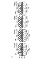
- FIG. 1 is a plan view schematically showing a TFT having a one-side LDD structure provided in the semiconductor device according to the first embodiment.
- 2 is a cross-sectional view showing a cross-sectional structure taken along the line II-II in FIG. 3A to 3C are cross-sectional views corresponding to FIG. 2 showing a semiconductor layer forming step in the method of manufacturing a semiconductor device according to the first embodiment.
- 4 is a cross-sectional view of a portion corresponding to FIG. 2 showing a gate insulating film forming step and an impurity level adjusting step in the method of manufacturing a semiconductor device according to the first embodiment.
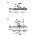
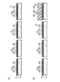
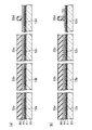
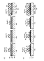
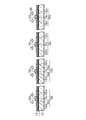
- FIGS. 5A to 5C are cross-sectional views corresponding to FIG.
- FIG. 6 is a plan view schematically showing a configuration of a gray tone mask used in the method for manufacturing a semiconductor layer according to the first embodiment.
- FIGS. 7A and 7B are cross-sectional views corresponding to FIG. 2 showing the latter half of the gate electrode formation step in the method for manufacturing the semiconductor device according to the first embodiment.
- 8A and 8B are cross-sectional views corresponding to FIG. 2 showing an n-type high concentration impurity region forming step in the method of manufacturing a semiconductor device according to the first embodiment.
- FIG. 9 is a cross-sectional view of a portion corresponding to FIG.
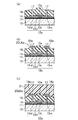
- FIGS. 10A to 10C are cross-sectional views corresponding to FIG. 2 showing respective steps after the interlayer insulating film forming step in the method of manufacturing a semiconductor device according to the first embodiment.
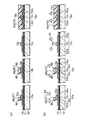
- FIG. 11 is a cross-sectional view showing a cross-sectional structure of a one-side offset TFT provided in a semiconductor device according to a modification of the first embodiment.
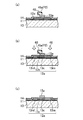
- 12A to 12C are cross-sectional views corresponding to FIG. 11 showing an n-type high-concentration impurity region forming step in the semiconductor device manufacturing method according to the modification of the first embodiment.
- FIG. 13A to 13C are cross-sectional views showing respective steps after the interlayer insulating film forming step in the method for manufacturing a semiconductor device according to the modification of the first embodiment.
- FIG. 14 is a plan view schematically showing a TFT having a double-sided LDD structure provided in the semiconductor device according to the second embodiment.
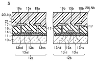
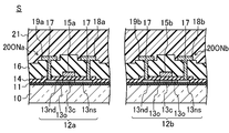
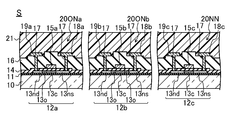
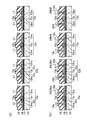
- FIG. 15 is a cross-sectional view illustrating a cross-sectional structure of a single-side LDD structure TFT and a double-side LDD structure TFT included in the semiconductor device according to the second embodiment in order from the left side in the drawing.
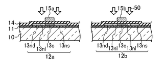
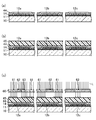
- 16 is a cross-sectional view of a portion corresponding to FIG. 15 showing a semiconductor layer forming step in the method for manufacturing a semiconductor device according to the second embodiment.
- FIG. 17 is a cross-sectional view of a portion corresponding to FIG. 15 showing a gate insulating film forming step and an impurity level adjusting step in the method of manufacturing a semiconductor device according to the second embodiment.
- FIGS. 18A to 18C are cross-sectional views corresponding to FIG. 15 showing the first half of the gate electrode formation step in the method of manufacturing a semiconductor device according to the second embodiment.
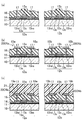
- FIGS. 19A and 19B are cross-sectional views corresponding to FIG. 15 showing the latter half of the gate electrode formation step in the method for manufacturing a semiconductor device according to the second embodiment.
- FIGS. 20A and 20B are cross-sectional views corresponding to FIG.
- FIG. 15 showing an n-type high concentration impurity region forming step in the method of manufacturing a semiconductor device according to the second embodiment.
- FIG. 21 is a cross-sectional view corresponding to FIG. 15 showing an n-type low-concentration impurity region forming step in the method for manufacturing a semiconductor device according to the second embodiment.
- 22A to 22C are cross-sectional views corresponding to FIG. 15 showing respective steps after the interlayer insulating film forming step in the semiconductor device manufacturing method according to the second embodiment.
- FIG. 21 is a cross-sectional view corresponding to FIG. 15 showing an n-type high concentration impurity region forming step in the method of manufacturing a semiconductor device according to the second embodiment.
- FIG. 21 is a cross-sectional view corresponding to FIG. 15 showing an n-type low-concentration impurity region forming step in the method for manufacturing a semiconductor device according to the second embodiment.
- 22A to 22C are cross-sectional views corresponding to FIG. 15 showing respective steps after the inter
- FIG. 23 shows a cross-sectional structure of a TFT with a single-side offset structure and a TFT with a double-side offset structure (offset structure having offset regions on both sides of a channel region) included in a semiconductor device according to a modification of Embodiment 2 in order from the left side in the drawing.
- 24A to 24C are cross-sectional views corresponding to FIG. 23 showing the n-type high concentration impurity region forming step in the method of manufacturing a semiconductor device according to the modification of the second embodiment.
- 25 (a) to 25 (c) are cross-sectional views corresponding to FIG. 23 showing respective steps after the interlayer insulating film forming step in the method of manufacturing a semiconductor device according to the modification of the second embodiment.
- FIG. 26 is a plan view schematically showing an n-type TFT having a normal structure provided in the semiconductor device according to the third embodiment.
- FIG. 27 is a cross-sectional view illustrating a cross-sectional structure of an n-type TFT having a single-side LDD structure, an n-type TFT having a double-sided LDD structure, and an n-type TFT having a normal structure included in the semiconductor device according to the third embodiment in order from the left side.
- 28 is a cross-sectional view of a portion corresponding to FIG. 27 showing a semiconductor layer forming step in the method for manufacturing a semiconductor device according to the third embodiment.
- 29 is a cross-sectional view of a portion corresponding to FIG.
- FIGS. 30A to 30C are cross-sectional views corresponding to FIG. 27 showing the first half of the gate electrode formation step in the method of manufacturing a semiconductor device according to the third embodiment.
- FIGS. 31A and 31B are cross-sectional views corresponding to FIG. 27 showing the latter half of the gate electrode formation step in the method of manufacturing a semiconductor device according to the third embodiment.
- 32 (a) and 32 (b) are cross-sectional views corresponding to FIG. 27 showing the n-type high concentration impurity region forming step in the method of manufacturing a semiconductor device according to the third embodiment.
- FIG. 33 is a cross-sectional view of a portion corresponding to FIG. 27 showing an n-type low concentration impurity region forming step in the method for manufacturing a semiconductor device according to the third embodiment.
- FIGS. 34A to 34C are cross-sectional views corresponding to FIG. 27 showing respective steps after the interlayer insulating film forming step in the method of manufacturing a semiconductor device according to the third embodiment.
- FIG. 35 is a cross-sectional view showing the cross-sectional structure of an n-type TFT with a one-side offset structure, an n-type TFT with a double-side offset structure, and an n-type TFT with a normal structure included in a semiconductor device according to a modification of the third embodiment in order from the left side in the figure. It is.
- FIGS. 36A to 36C are cross-sectional views corresponding to FIG. 35 showing the n-type high concentration impurity region forming step in the method for manufacturing a semiconductor device according to the modification of the third embodiment.
- FIGS. 37A to 37C are cross-sectional views corresponding to FIG. 35 showing respective steps after the interlayer insulating film forming step in the method for manufacturing a semiconductor device according to the modification of the third embodiment.
- FIG. 36A to 36C are cross-sectional views corresponding to FIG. 35 showing the n-type high concentration impurity region forming step in the method for manufacturing a semiconductor device according to the modification of the third embodiment.
- FIGS. 37A to 37C are cross-sectional views corresponding to FIG. 35 showing respective steps after the interlayer insulating film forming step in the method for manufacturing a semiconductor device according to the modification of the third embodiment.
- FIG. 38 is a cross-sectional view of an n-type TFT having a single-side LDD structure, an n-type TFT having a double-sided LDD structure, an n-type TFT having a normal structure, and a p-type TFT having a normal structure provided in the semiconductor device according to the fourth embodiment from the left side of the drawing. It is sectional drawing shown in order.
- FIG. 39 is a cross-sectional view of a portion corresponding to FIG. 38 showing a semiconductor layer forming step in the method for manufacturing a semiconductor device according to the fourth embodiment.
- 40 is a cross-sectional view of a portion corresponding to FIG. 38 showing a gate insulating film formation step in the method for manufacturing a semiconductor device according to the fourth embodiment.
- 41A and 41B are cross-sectional views corresponding to FIG. 38 showing the conductivity type adjusting step in the method of manufacturing a semiconductor device according to the fourth embodiment.
- 42A and 42B are cross-sectional views corresponding to FIG. 38 showing the first half of the first gate electrode formation step in the method for manufacturing a semiconductor device according to the fourth embodiment.
- FIGS. 43A and 43B are cross-sectional views corresponding to FIG. 38 showing the latter half of the first gate electrode formation step in the method of manufacturing a semiconductor device according to the fourth embodiment.
- FIG. 44 is a cross-sectional view of a portion corresponding to FIG. 38 showing a p-type high concentration impurity region forming step in the method for manufacturing a semiconductor device according to the fourth embodiment.
- 45A and 45B are cross-sectional views corresponding to FIG. 38 showing the first half of the second gate electrode formation step in the method for manufacturing a semiconductor device according to the fourth embodiment.
- 46A and 46B are cross-sectional views corresponding to FIG. 38 illustrating the latter half of the second gate electrode formation step in the method for manufacturing a semiconductor device according to the fourth embodiment.
- 47A and 47B are cross-sectional views corresponding to FIG. 38 showing the n-type high concentration impurity region forming step in the method of manufacturing a semiconductor device according to the fourth embodiment.
- 48 is a cross-sectional view of a portion corresponding to FIG. 38 showing an n-type low concentration impurity region forming step in the method for manufacturing a semiconductor device according to the fourth embodiment.
- FIG. 50 is a cross-sectional view of an n-type TFT having a one-side offset structure, an n-type TFT having a both-side offset structure, an n-type TFT having a normal structure, and a p-type TFT having a normal structure provided in a semiconductor device according to a modification of the fourth embodiment. It is sectional drawing shown in order from the middle left side. 51A and 51B are cross-sectional views corresponding to FIG.
- 52 (a) and 52 (b) are cross-sectional views corresponding to FIG. 50 showing respective steps after the interlayer insulating film forming step in the method of manufacturing a semiconductor device according to the modification of the fourth embodiment.
- FIG. 1 is a schematic plan view of an n-type TFT having a one-side LDD structure provided in the semiconductor device S according to the first embodiment.
- 2 is a cross-sectional view showing a cross-sectional structure taken along the line II-II in FIG.
- the semiconductor device S of this embodiment includes an insulating substrate 10 such as a glass substrate as a base substrate, and an n-side LDD structure n shown in FIG. 1 provided on the insulating substrate 10.
- Type TFT 20LNa The semiconductor device S is, for example, an active matrix substrate constituting an active matrix driving type liquid crystal display device, and an n-type TFT 20LNa having a one-side LDD structure functions as an active element of a driving circuit such as a gate driver or a source driver. It is.
- the n-type TFT 20LNa having the one-side LDD structure has a top gate type structure in which a gate electrode 15a is disposed on the side opposite to the insulating substrate 10 side of the semiconductor layer 12a.
- a base insulating film 11 is provided on the entire surface of the insulating substrate 10.
- the n-type TFT 20LNa having a one-side LDD structure includes a semiconductor layer 12a provided on the insulating substrate 10 via the base insulating film 11, a gate insulating film 14 provided so as to cover the semiconductor layer 12a, A gate electrode 15a provided so as to overlap the central portion of the semiconductor layer 12a via the gate insulating film 14, and a source electrode 18a connected to the semiconductor layer 12a so as to be spaced apart from each other at a position sandwiching the gate electrode 15a. And a drain electrode 19a (indicated by a two-dot chain line in FIG. 1).
- the base insulating film 11 is formed by sequentially laminating a silicon nitride film and a silicon oxide film, for example.
- the semiconductor layer 12a is made of a crystalline semiconductor such as polysilicon.
- the semiconductor layer 12a has a channel region 13c corresponding to the gate electrode 15a, and an n-type high concentration impurity region 13ns that functions as a source region without being spaced from the channel region 13c on one side of the channel region 13c.
- An n-type high concentration impurity region 13nd functioning as a drain region is formed on the other side of the channel region 13c at a predetermined interval from the channel region 13c.
- An n-type low-concentration impurity region 13nl called an LDD region is formed between one n-type high-concentration impurity region 13nd that functions as a drain region in the semiconductor layer 12a and the channel region 13c.
- the channel region 13c contains p-type impurities such as boron (B) in order to control the threshold voltage.
- Each n-type high concentration impurity region 13ns, 13nd contains n-type impurities such as phosphorus (P).
- the n-type low-concentration impurity region 13nl contains an n-type impurity such as phosphorus (P) at a lower concentration than the n-type high-concentration impurity regions 13ns and 13nd.
- the gate insulating film 14 is made of, for example, silicon nitride or silicon oxide.
- the gate electrode 15a is made of, for example, aluminum (Al), tantalum (Ta), titanium (Ti), molybdenum tungsten (MoW), or chromium (Cr).
- an interlayer insulating film 16 is provided on the gate insulating film 14 so as to cover the gate electrode 15a.
- the interlayer insulating film 16 and the gate insulating film 14 penetrate through both the insulating films 14 and 16 at locations corresponding to the pair of n-type high concentration impurity regions 13ns and 13nd in the semiconductor layer 12a.
- a contact hole 17 reaching 12a is formed.
- These contact holes 17 are filled with a conductive material such as aluminum (Al), tantalum (Ta), titanium (Ti), molybdenum tungsten (MoW), or chromium (Cr).
- a conductive material such as aluminum (Al), tantalum (Ta), titanium (Ti), molybdenum tungsten (MoW), or chromium (Cr).
- Al aluminum
- Ta tantalum
- Ti titanium
- MoW molybdenum tungsten
- Cr chromium
- the source electrode 18a is connected through one contact hole 17 to an n-type high concentration impurity region 13ns that functions as a source region.
- the drain electrode 19a is connected to the n-type high concentration impurity region 13nd functioning as a drain region through the other contact hole 17.
- the source electrode 18a and the drain electrode 19a are made of the same material as the conductive material.
- the n-type TFT 20LNa having the one-side LDD structure described above is covered with a protective insulating film 21.
- the protective insulating film 21 is made of, for example, an acrylic-based organic insulating material.
- conductive portions such as electrodes and wirings are formed on the protective insulating film 21 as necessary. This conductive portion is connected to, for example, the drain electrode 19a of the TFT 20LNa through a contact hole formed in the protective insulating film 21.
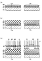
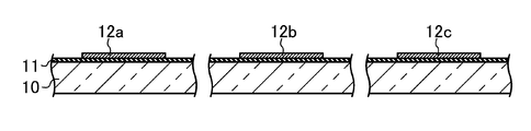
- FIG. 3A to 3C are cross-sectional views showing a semiconductor layer forming process.
- FIG. 4 is a cross-sectional view showing a gate insulating film forming step and an impurity level adjusting step.
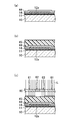
- 5A to 5C are cross-sectional views showing the first half steps of the gate electrode formation process.
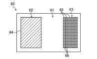
- FIG. 6 is a schematic plan view of the gray tone mask 60 used in the gate electrode forming process.
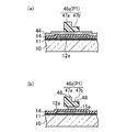
- 7A and 7B are cross-sectional views showing the latter half of the gate electrode formation process.
- 8A and 8B are cross-sectional views showing an n-type high concentration impurity region forming step.
- FIG. 9 is a cross-sectional view showing an n-type low concentration impurity region forming step.
- FIG. 10A to 10C are cross-sectional views showing respective steps after the interlayer insulating film forming step. 3 (a) to (c) to FIG. 5 (a) to (c) and FIG. 7 (a), (b) to FIG. 10 (a) to (c) respectively show corresponding parts in FIG. ing.
- the manufacturing method of the semiconductor device S includes a base insulating film forming step, a semiconductor layer forming step, a gate insulating film forming step, an impurity level adjusting step, a gate electrode forming step, an n-type high It includes a concentration impurity region forming step, an n-type low concentration impurity region forming step, an interlayer insulating film forming step, a source / drain electrode forming step, and a protective insulating film forming step.
- ⁇ Base insulating film formation process First, an insulating substrate 10 such as a glass substrate serving as a base substrate is prepared. Then, a silicon nitride film and a silicon oxide film are sequentially formed on the prepared insulating substrate 10 by a CVD (Chemical Vapor Deposition) method, thereby forming a base insulating film 11 in which these are laminated.
- CVD Chemical Vapor Deposition
- an amorphous silicon film 40 (for example, a thickness of 40 nm to 50 nm) is formed on the substrate on which the base insulating film 11 is formed by LPCVD (Low Pressure CVD). Film).
- the amorphous silicon film 40 is crystallized as shown in FIG. 3B by irradiating the amorphous silicon film 40 with a laser beam 41 such as an excimer laser or a YAG (Yttrium Aluminum Garnet) laser.
- the polysilicon film 42 is a kind of crystalline semiconductor film.
- the polysilicon film 42 is patterned by photolithography using a first photomask, thereby forming a semiconductor layer 12a as shown in FIG.
- the energy level of the semiconductor layer 12a is biased toward the donor level due to the influence of the base insulating film 11.
- the amorphous silicon film 40 is crystallized by laser irradiation to form the polysilicon film 42, but the present invention is not limited to this.
- the polysilicon film 42 is, for example, a solid phase that crystallizes the amorphous silicon film 40 by performing a heat treatment after adding a metal element such as nickel (Ni) as a catalyst element for promoting crystallization to the amorphous silicon film 40. It may be formed by a growth method (SPC; Solid Phase Crystallization), or may be formed by other known methods.
- This semiconductor layer forming step corresponds to the semiconductor layer forming step in the present invention.
- a silicon nitride film or a silicon oxide film (for example, a thickness of about 50 nm to 120 nm) covering the semiconductor layer 12a is formed on the substrate on which the semiconductor layer 12a is formed by CVD, as shown in FIG. This is referred to as a gate insulating film 14.
- This gate insulating film forming step corresponds to the gate insulating film forming step in the present invention.
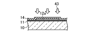
- the impurity level in the semiconductor layer 12a is changed to the acceptor level, and the depth of the conductive level in the channel region 13c formed later brings a predetermined threshold voltage to the n-type TFT 20LNa formed by the semiconductor layer 12a. Adjust as follows. An arrow 43 shown in FIG. 4 indicates the boron (B) injection direction at this time.
- this impurity level adjustment step is not necessarily performed, and may be performed as necessary in consideration of the type and depth of the impurity levels of the semiconductor layer 12a.
- ⁇ Gate electrode formation process> As shown in FIG. 5A, for example, aluminum (Al), tantalum (Ta), titanium (Ti), molybdenum tungsten is formed on the substrate including the semiconductor layer 12a having the adjusted impurity level by sputtering. A metal film made of (MoW), chromium (Cr), or the like, or a laminated film thereof is formed and used as a conductive film 44 for forming a gate electrode (conductive film formation step).
- Al aluminum
- Ta tantalum
- Ti titanium
- Mo molybdenum tungsten
- a metal film made of (MoW), chromium (Cr), or the like, or a laminated film thereof is formed and used as a conductive film 44 for forming a gate electrode (conductive film formation step).
- a positive photosensitive resin is applied on the conductive film 44 for forming the gate electrode by spin coating or slit coating to form a photosensitive resin film 45 (for example, thick). Film is formed (photosensitive resin film forming step).
- the exposure process is performed by controlling the exposure amount irradiated to the uncured photosensitive resin film 45 using the second photomask.
- a gray tone mask 60 shown in FIG. 6 which is a kind of multi-tone mask is used as the second photomask.
- the gray tone mask 60 includes a translucent portion 63 that blocks part of light, in addition to a transmissive portion 61 that transmits light and a light-shielding portion 62 that does not transmit light at all.
- a light shielding film 64 is formed on the entire surface of the light shielding portion 62.
- the semi-transmissive portion 63 a large number of light shielding layers 65 are arranged in stripes, and slits 66 having a resolution lower than that of the exposure machine are formed between the light shielding layers 65.
- the light-shielding portion 62 has a gate electrode corresponding to the semiconductor layer 12a when the gray-tone mask 60 is disposed at a predetermined position facing the photosensitive resin film 45. It is formed so as to be located on one side (left side in FIG. 5C) on the formation region.
- the semi-transmissive portion 63 is also located on the other side of the gate electrode formation region corresponding to the semiconductor layer 12a (FIG. 5) when the gray tone mask 60 is disposed at a predetermined position facing the photosensitive resin film 45. It is formed so as to be located on the right side in (c).
- the gray tone mask 60 When exposure processing is performed on the photosensitive resin film 45, the gray tone mask 60 is disposed at the predetermined position so as to face the photosensitive resin film 45 as shown in FIG. 5C. Thereafter, ultraviolet rays L are irradiated from the opposite side of the gray tone mask 60 to the insulating substrate 10. Then, the photosensitive resin film 45 is exposed through the gray tone mask 60.
- the photosensitive resin film 45 portion has a stripe shape.
- the exposure amount is reduced by the light shielding layer 65 and the exposure is performed with an exposure amount smaller than that of the transmission portion 61 on the average.
- one side portion (the left side portion in FIG. 5C) of the gate electrode formation region that is the location opposite to the light shielding portion 62 is not exposed at all, and the portion that faces the semi-transmissive portion 63 is not exposed.
- the other side portion of the gate electrode formation region (the right side portion in FIG. 5C) is exposed with a smaller exposure amount than the portion facing the transmission portion 61.
- the photosensitive resin film 45 is patterned to form resist layers 46a having different thicknesses on one side and the other side for forming the gate electrode as shown in FIG. 7A (photosensitive resin film). Patterning step).
- a relatively thick film portion 47a (for example, about 1 ⁇ m to 2 ⁇ m in thickness) is formed on the source region formation side.
- a resist layer 46a having a relatively thin thin film portion 47b (for example, a thickness of about 0.5 ⁇ m to 1 ⁇ m) on the side to be formed and slightly wider than the gate electrode 15a to be formed is formed.
- the resist layer 46a constitutes a first resist pattern P1.
- the conductive film 44 is patterned by isotropic wet etching, thereby forming a gate electrode 15a at a location corresponding to the semiconductor layer 12a as shown in FIG. 7B. (Conductive film patterning step).
- the etching time is adjusted, and the conductive film 44 overlapping the peripheral edge of the resist layer 46a is also removed by side etching, and the gate electrode 15a is retracted to the inside of the resist layer 46a to be narrower than the resist layer 46a.
- the resist layer 46a is formed with an overhanging portion 48 that protrudes in a hook shape on both sides of the gate electrode 15a.
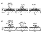
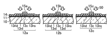
- ⁇ N-type high concentration impurity region forming step> The resist layer 46a is gradually retreated from the surface side by ashing, and ashing is stopped when the entire thin film portion 47b is removed as shown in FIG. 8A (thin film portion removing step).
- the thin film portion 47b is completely removed, and the thick film portion 47a is left thin, and the resist layer 26a is formed in a shape in which the overhang portion 48 projects only on one side of the gate electrode 15a.
- the resist layer 46a consisting of the thick film portion remaining at this stage forms the second resist pattern P2.
- phosphorus (P) is implanted at a high concentration as an n-type impurity into the semiconductor layer 12a by ion doping using the resist layer 46a and the gate electrode 15a as a mask, as shown in FIG. High concentration impurity implantation step; impurity implantation step).
- An arrow 49 shown in FIG. 8B indicates the injection direction of phosphorus (P) at this time.
- n-type high-concentration impurity regions 13ns and 13nd functioning as a source region and a drain region are formed on both sides of the semiconductor layer 12a corresponding to the resist layer 46a and the gate electrode 15a.
- the source region is formed on one side (right side in FIG. 8B) of the channel region forming portion 13c ′ formed by the portion corresponding to the gate electrode 15a without being spaced from the channel region forming portion 13c ′.
- N-type high-concentration impurity region 13 ns functioning as a resist layer 46 a is projected from the channel region formation portion 13 c ′ to the other side (left side in FIG. 8B) of the channel region formation portion 13 c ′.
- An n-type high-concentration impurity region 13nd that functions as a drain region is formed at an interval corresponding to the protruding portion of the portion 48.
- An offset region 13o in which no impurity is implanted is formed between the n-type high concentration impurity region 13nd functioning as the drain region in the semiconductor layer 12a and the channel region forming portion 13c '.
- ⁇ N-type low concentration impurity region forming step> After forming the n-type high concentration impurity regions 13ns and 13nd in the semiconductor layer 12a as described above, the remaining resist layer 46a is completely removed by resist stripping solution, ashing or the like (resist layer removing step).
- phosphorus (P) is implanted at a low concentration as an n-type impurity into the semiconductor layer 12a by ion doping as shown in FIG. 9 (low concentration impurity implantation step).
- An arrow 50 shown in FIG. 9 indicates the injection direction of phosphorus (P) at this time.
- phosphorus (P) is additionally implanted into the n-type high concentration impurity regions 13 ns and 13 nd of the semiconductor layer 12 a.
- phosphorus (P) is also implanted into the offset region 13o to form an n-type low concentration impurity region 13nl in the offset region 13o.
- a channel region 13c is formed in a self-aligned manner at a portion corresponding to the gate electrode 15a of the semiconductor layer 12a.
- Interlayer insulating film formation process A silicon nitride film and a silicon oxide film are sequentially formed by a CVD method on a substrate including the semiconductor layer 12a in which the channel region 13c, the n-type low-concentration impurity region 13nl, and the n-type high-concentration impurity regions 13ns and 13nd are formed. Then, an interlayer insulating film 16 composed of these laminated films is formed.
- a metal film made of, for example, aluminum (Al), tantalum (Ta), titanium (Ti), molybdenum tungsten (MoW), or chromium (Cr) is formed on the substrate on which the interlayer insulating film 16 is formed by sputtering.
- a laminated film of these is formed and used as a conductive film for forming the source electrode 18a and the drain electrode 19a.
- the conductive film is patterned by photolithography using a fourth photomask to form the source electrode 18a and the drain electrode 19a as shown in FIG. 10B.
- an insulating film is formed by applying an acrylic-based organic insulating resin by spin coating or slit coating.
- this uncured insulating film is subjected to exposure processing using a fifth photomask and then developed to be patterned to form a protective insulating film 21 as shown in FIG.
- a contact hole for making contact between the drain electrode 19a of the n-type TFT 20LNa having a one-side LDD structure and the conductive portion is provided. Form it.
- an electrode or a wiring is connected to the TFT 20LNa through the contact hole formed earlier on the substrate on which the protective insulating film 21 is formed by photolithography using a sixth photomask. Etc. are formed.
- the semiconductor device S including the n-type TFT 20LNa having a one-side LDD structure can be manufactured.
- two photo resist patterns P1 and P2 with a single photomask that is, the thick film portion 47a in the gate electrode forming step and the n-type high concentration impurity region forming step, and A first resist pattern P1 composed of a resist layer 46a having a thin film portion 47b, and a second resist pattern P2 composed of a resist layer 46a of only a thin film portion constituting portion formed in the n-type low concentration impurity region forming step.
- the first resist pattern P1 is used as a mask for forming the gate electrode 15a
- the second resist pattern P2 is used as a mask for forming the low-concentration impurity region 13nl for impurity implantation into the semiconductor layer 12a. Therefore, the resist layer 46a for forming the gate electrode 15a and the resist for injecting impurities into the semiconductor layer 12a A photomask required for the formation of the 46a can be finished in one piece.
- the line width variation of the gate electrode 15a due to side etching is dominant, and another factor that greatly affects the line width of the low concentration impurity region 13nl.
- variations in line width of the low concentration impurity region 13nl can be suppressed.
- the high concentration impurity is implanted into the semiconductor layer 12a only through the gate insulating film 14, the variation in the sheet resistance of the low concentration impurity region 13nl is caused by the high concentration impurity passing through the gate electrode as described in Patent Document 2. This can be suppressed as compared with the case of performing injection. As a result, it is possible to stably obtain an n-type TFT 20LNa having a single-side LDD structure with good characteristics by minimizing factors causing variations in TFT characteristics.
- the semiconductor device S including the n-type TFT 20LNa can be manufactured at a low cost by suppressing the number of steps with a small number of photomasks. be able to.
- FIG. 11 is a cross-sectional view showing a cross-sectional structure of an n-type TFT 20ONa having a one-side offset structure provided in the semiconductor device S according to this modification.
- the semiconductor device S of this modification includes an n-type TFT 20ONa having a one-side offset structure instead of the n-type TFT 20LNa having a one-side LDD structure.
- This one-side offset structure TFT 20ONa has the same top-gate structure as the one-side LDD structure n-type TFT 20LNa.
- a channel region 13c is provided at a portion corresponding to the gate electrode 15a, and n-type high-concentration impurity regions 13ns and 13nd functioning as a source region and a drain region on both sides of the channel region 13c.
- An offset region 13o is formed between the n-type high-concentration impurity region 13nd and the channel region 13c, which functions as a drain region in the semiconductor layer 12a, instead of the n-type low-concentration impurity region 13nl.
- the offset region 13o also contains p-type impurities such as boron (B), like the channel region 13c, and has the same impurity concentration as the channel region 13c.
- 12A to 12C are cross-sectional views showing an n-type high concentration impurity region forming step.
- 13A to 13C are cross-sectional views showing respective steps after the interlayer insulating film forming step. 12 (a) to 12 (c) and FIGS. 13 (a) to 13 (c) respectively show portions corresponding to FIG.
- the manufacturing method of the semiconductor device S according to this modification includes a base insulating film forming step, a semiconductor layer forming step, a gate insulating film forming step, an impurity level adjusting step, a gate electrode forming step, an n-type high It includes a concentration impurity region forming step, an interlayer insulating film forming step, a source / drain electrode forming step, and a protective insulating film forming step, and does not include an n-type low concentration impurity region forming step.
- the base insulating film forming step, the semiconductor layer forming step, the gate insulating film forming step, the impurity level adjusting step, and the gate electrode forming step are the same as those in the first embodiment, detailed description thereof is omitted.
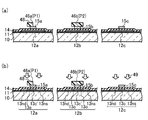
- ⁇ N-type high concentration impurity region forming step> After the gate electrode 15a is formed in the gate electrode formation step, the resist layer 46a is gradually retreated from the surface side by ashing, and when the entire thin film portion 47b is removed as shown in FIG. Stop ashing (thin film portion removal step).
- the thin film portion 47b is completely removed, and the thick film portion 47a is left thin, and the resist layer 26a is formed in a shape in which the overhang portion 48 projects only on one side of the gate electrode 15a.
- the resist layer 46a consisting of the thick film portion remaining at this stage forms the second resist pattern P2.
- phosphorus (P) is implanted at a high concentration as an n-type impurity into the semiconductor layer 12a by ion doping as shown in FIG. Injection step).
- n-type high concentration impurity regions 13ns and 13nd functioning as a source region and a drain region are formed on both sides of the semiconductor layer 12a corresponding to the resist layer 46a and the gate electrode 15a.
- the n-type high concentration impurity region 13nd functioning as the drain region is formed at a distance corresponding to the protruding portion of the protruding portion 48 of the resist layer 46a from the portion corresponding to the gate electrode 15a.
- a channel region 13c is formed at a position corresponding to the gate electrode 15a of the semiconductor layer 12a, and an offset region 13o is formed between the channel region 13c and the n-type high concentration impurity region 13nd functioning as a drain region.
- the remaining resist layer 46a is completely removed by resist stripping solution or ashing.
- the semiconductor device S including the TFT 20ONa having the one-side offset structure is manufactured without implanting impurities in each step after the formation of the n-type high concentration impurity regions 13ns and 13nd with respect to the offset region 13o of the semiconductor layer 12a. can do.
- FIG. 14 is a schematic plan view showing an n-type TFT 20LNb having a double-sided LDD structure provided in the semiconductor device S according to the second embodiment.
- FIG. 15 is a cross-sectional view illustrating a cross-sectional structure of an n-type TFT 20LNa having a single-side LDD structure and an n-type TFT 20LNb having a double-sided LDD structure in order from the left side in the drawing.
- a cross-sectional view of the n-type TFT 20LNb having a double-sided LDD structure shows a cross-sectional structure taken along line XV-XV in FIG.
- the same components as those in FIGS. 1 to 13 (a) to 13 (c) will be given the same reference numerals, and the detailed description will be given. Omitted.
- the semiconductor device S includes a double-sided LDD structure TFT 20 ⁇ / b> LNb on the insulating substrate 10 in addition to the single-side LDD structure TFT 20 ⁇ / b> LNa.
- the n-type TFT 20LNa having a one-side LDD structure has the same configuration as the n-type TFT 20LNa having the same structure described in the first embodiment, and includes a first semiconductor layer 12a corresponding to the semiconductor layer 12a.
- the n-type TFT 20LNb having a double-sided LDD structure has the same top-gate structure as the n-type TFT 20LNa having a single-side LDD structure, as shown in FIGS. 14 and 15.
- the base insulating film 11 is formed on the insulating substrate 10.
- the second semiconductor layer 12b provided via the gate insulating film 14, the gate insulating film 14 provided so as to cover the second semiconductor layer 12b, and the central portion of the second semiconductor layer 12b overlapping the gate insulating film 14
- a source electrode 18b and a drain electrode 19b (shown by a two-dot chain line in FIG. 14) connected to the second semiconductor layer 12b at a position sandwiching the gate electrode 15b. It has.
- the second semiconductor layer 12b is made of the same crystalline semiconductor such as polysilicon as the first semiconductor layer 12a.
- the second semiconductor layer 12b has a channel region 13c corresponding to the gate electrode 15a and a pair of n that functions as a source region and a drain region on both sides of the channel region 13c with a predetermined distance from the channel region 13c.
- Type high concentration impurity regions 13ns and 13nd are formed, respectively.
- an n-type low concentration impurity region 13nl is formed between the channel region 13c and the n-type high concentration impurity regions 13ns and 13nd.
- an n-type impurity such as phosphorus (P) or boron
- P phosphorus
- B boron
- a common film is used for the n-type TFT having the one-side LDD structure and the n-type TFT 20LNb having the both-side LDD structure.
- the gate electrode 15b of the n-type TFT 20LNb having a double-sided LDD structure is made of the same material as the gate electrode 15a of the n-type TFT 20LNa having a single-side LDD structure.
- the source electrode 18b and the drain electrode 19b of the n-type TFT 20LNb having the double-sided LDD structure are also made of the same material as the source electrode 18a and the drain electrode 19a of the n-type TFT 20LNa having the one-side LDD structure.
- FIG. 16 is a cross-sectional view showing the semiconductor layer forming step.
- FIG. 17 is a cross-sectional view showing a gate insulating film forming step and an impurity level adjusting step.
- 18 and 19 are cross-sectional views showing the gate electrode forming step.
- FIG. 20 is a cross-sectional view showing the n-type high concentration impurity region forming step.
- FIG. 21 is a cross-sectional view showing the n-type low concentration impurity region forming step.
- 22A to 22C are cross-sectional views showing respective steps after the interlayer insulating film forming step. Note that FIGS. 16 to 22 (a) to 22 (c) respectively show portions corresponding to FIG.
- the manufacturing method of the semiconductor device S includes a base insulating film forming step, a semiconductor layer forming step, a gate insulating film forming step, an impurity level adjusting step, a gate electrode forming step, an n-type high It includes a concentration impurity region forming step, an n-type low concentration impurity region forming step, an interlayer insulating film forming step, a source / drain electrode forming step, and a protective insulating film forming step.
- the polysilicon film 42 is patterned by photolithography using the first photomask, so that the first semiconductor layer as shown in FIG. 12a and the second semiconductor layer 12b are formed (semiconductor layer forming step). Also in this embodiment, at this stage, the energy levels of the first semiconductor layer 12a and the second semiconductor layer 12b are influenced by the base insulating film 11 and are biased toward the donor level.
- a gate insulating film 14 is formed on the substrate on which the first semiconductor layer 12a and the second semiconductor layer 12b are formed, as shown in FIG. 17 (deposition of the gate insulating film). Step).
- boron (B) is implanted at a low concentration as a p-type impurity into the entire first semiconductor layer 12a and second semiconductor layer 12b covered with the gate insulating film.
- the impurity level in the first semiconductor layer 12a and the second semiconductor layer 12b is changed to the acceptor level, and the depth of the conductive level in the channel region 13c to be formed later constitutes each of the semiconductor layers 12a and 12b.
- the n-type TFTs 20LNa and 20LNb are adjusted so as to bring a predetermined threshold voltage.
- this impurity level adjustment step is not necessarily performed, and may be performed as necessary in consideration of the types and depths of the impurity levels of the first semiconductor layer 12a and the second semiconductor layer 12b.
- a positive photosensitive resin is applied on the conductive film 44 for forming the gate electrode in the same manner as in the first embodiment, and a photosensitive resin film 45 (for example, thick) is applied. Film is formed (photosensitive resin film forming step).
- an exposure process is performed by controlling the amount of exposure with which the uncured photosensitive resin film 45 is irradiated using a second photomask.
- a gray tone mask 60 shown in FIG. 6 which is a kind of multi-tone mask is used as the second photomask.
- the light-shielding portion 62 has a portion corresponding to the first semiconductor layer 12a when the gray-tone mask 60 is disposed at a predetermined position facing the photosensitive resin film 45. It is formed so as to be located on one side (left side in FIG. 18C) on the gate electrode formation region and on the gate electrode formation region corresponding to the second semiconductor layer 12b.
- the semi-transmissive portion 63 is also formed on the other side (on the gate electrode formation region corresponding to the first semiconductor layer 12a) when the gray tone mask 60 is disposed at a predetermined position facing the photosensitive resin film 45. It is formed so as to be located on the right side in FIG.
- the gray tone mask 60 When exposure processing is performed on the photosensitive resin film 45, the gray tone mask 60 is disposed at the predetermined position facing the photosensitive resin film 45 as shown in FIG. 18C. Thereafter, ultraviolet rays L are irradiated from the opposite side of the gray tone mask 60 to the insulating substrate 10. Then, the photosensitive resin film 45 is exposed through the gray tone mask 60.
- the entire gate electrode 15b formation region corresponding to 12c is not exposed at all, and the other side portion of the gate electrode 15a formation region corresponding to the first semiconductor layer 12a corresponding to the semi-transmissive portion 63 (FIG. 18C).
- photosensitive resin film patterning step Thereafter, development processing is performed on the photosensitive resin film 45 subjected to the exposure processing (photosensitive resin film patterning step). Thereby, the photosensitive resin film 45 is patterned, and as shown in FIG. 19A, a first resist which is a resist layer similar to that of the first embodiment for forming the gate electrode corresponding to the first semiconductor layer 12a.
- a second resist layer 46b having a uniform thickness is formed on the layer 46a for forming a gate electrode corresponding to the second semiconductor layer 12b.
- the gate electrode formation region corresponding to the first semiconductor layer 12a has a thick film portion 47a on the drain region formation planned side and a thin film portion 47b on the source region formation planned side. Then, a first resist layer 46a that is slightly wider than the gate electrode 15a to be formed is formed. In addition, the second resist layer 46b having a uniform width that is slightly wider than the gate electrode 15b to be formed and has the same thickness as that of the thick film portion 47a is formed on the gate electrode formation region at the portion corresponding to the second semiconductor layer 12b. Form.
- the first resist layer 46a and the second resist layer 46b constitute a first resist pattern P1.
- the conductive film 44 is patterned by isotropic wet etching, as shown in FIG. 19B.
- Gate electrodes 15a and 15b are formed at locations corresponding to 12a and locations corresponding to the second semiconductor layer 12b, respectively (conductive film patterning step).
- the etching time is adjusted, and the conductive film 44 overlapping the peripheral portions of the first resist layer 46a and the second resist layer 46b is also removed by side etching, and each gate electrode 15a, 15b is removed from each resist layer 46a.
- , 46b are formed to be narrower than the corresponding first resist layer 46a or second resist layer 46b.
- the first resist layer 46a and the second resist layer 46b are respectively formed with overhang portions 48 extending in a hook shape on both sides of the gate electrodes 15a and 15b.
- ⁇ N-type high concentration impurity region forming step> The first resist layer 46a and the second resist layer 46b are retreated to removal from the surface side by ashing, and ashing is stopped when the entire thin film portion 47b is removed as shown in FIG. Part removal step).
- the first resist layer 46a has a shape in which the thin film portion 47b is completely removed and the thick film portion 47a is left thin, and the overhang portion 48 protrudes only on one side portion of the gate electrode 26a. . Further, the entire second resist layer 46b is left as a thin film.
- the first resist layer 46a and the second resist layer 46b left at this stage constitute a second resist pattern P2.
- ions are formed on the first semiconductor layer 12a using the first resist layer 46a and the gate electrode 15a formed of the thin film portion constituting portion as a mask, and on the second semiconductor layer 12b using the thinned second resist layer 46b as a mask.
- phosphorus (P) is implanted at a high concentration as an n-type impurity by doping (impurity implantation step; high concentration impurity implantation step).
- the first semiconductor layer 12a is not spaced from the channel region forming portion 13c ′ on one side (right side in FIG. 20B) of the channel region forming portion 13c ′ formed by the portion corresponding to the gate electrode 15a.
- An n-type high-concentration impurity region 13ns functioning as a source region is formed, and the first resist layer 46a is formed from the channel region formation portion 13c ′ to the other side (left side in FIG. 17B) of the channel region formation portion 13c ′.
- An n-type high concentration impurity region 13nd that functions as a drain region is formed at an interval corresponding to the protruding portion of the protruding portion 48.
- An offset region 13o in which no impurity is implanted is formed between the n-type high concentration impurity region 13nd functioning as the drain region in the first semiconductor layer 12a and the channel region forming portion 13c '.
- the second semiconductor layer 12b corresponds to the protruding portion of the protruding portion 48 of the second resist layer 46b from the channel region forming portion 13c ′ on both sides of the channel region forming portion 13c ′ formed by the portion corresponding to the gate electrode 15b.
- N-type high concentration impurity regions 13 ns and 13 nd functioning as a source region and a drain region are formed with an interval between them.
- An offset region 13o in which no impurity is implanted is formed between the channel region forming portion 13c 'in the second semiconductor layer 12b and the n-type high concentration impurity regions 13ns and 13nd.
- ⁇ N-type low concentration impurity region forming step> After forming the n-type high concentration impurity regions 13 ns and 13 nd in the first semiconductor layer 12 a and the second semiconductor layer 12 b as described above, the remaining first resist layer 46 a and second resist layer 46 b are removed from the resist stripping solution or ashing. The resist layer is completely removed (resist layer removal step).
- phosphorus (P) is implanted at a low concentration as an n-type impurity into the first semiconductor layer 12a and the second semiconductor layer 12b by ion doping as shown in FIG. (Low concentration impurity implantation step).
- phosphorus (P) is additionally implanted into the n-type high concentration impurity regions 13 ns and 13 nd of the first semiconductor layer 12 a and the second semiconductor layer 12 b.
- phosphorus (P) is also implanted into each offset region 13o in the first semiconductor layer 12a and the second semiconductor layer 12b, and an n-type low concentration impurity region 13nl is formed in each offset region 13o.
- Channel regions 13c are formed in a self-aligned manner at locations corresponding to the gate electrodes 15a and 15b of the first semiconductor layer 12a and the second semiconductor layer 2b, respectively.
- the semiconductor device S including the one-side LDD structure TFT 20LNa and the two-side LDD structure TFT 20LNb can be manufactured.
- Embodiment 2- the same effects as in the first embodiment can be obtained, and the one-side LDD structure TFT 20LNa and the two-side LDD structure TFT 20LNb can be formed together on the same substrate 10.
- the combination of these two types of LDD structure TFTs 20LNa and 20LNb greatly increases the types of circuits that can be formed, thereby increasing the degree of freedom in circuit design.
- the semiconductor device S having excellent performance can be realized by appropriately adopting n-type TFTs 20LNa and 20LNb having an LDD structure of a type according to required characteristics.
- FIG. 23 is a cross-sectional view illustrating the cross-sectional structures of the n-type TFT 20ONa having a one-side offset structure and the n-type TFT 20ONb having a double-sided LDD structure included in the semiconductor device S according to this modification in order from the left side in the drawing.
- the semiconductor device S of the present modification includes an n-type TFT 20ONa having a one-side offset structure instead of an n-type TFT 20LNa having a one-side LDD structure on an insulating substrate 10 and an n-type TFT 20LNb having a both-side LDD structure. Instead, an n-type TFT 20ONb having a double-sided LDD structure is provided.
- the n-type TFT 20ONa having a one-side offset structure has the same configuration as the TFT 20ONa having the same structure described in the modification of the first embodiment, and includes a first semiconductor layer 12a corresponding to the semiconductor layer 12a.
- the n-type TFT 20ONb having a both-side offset structure has the same top-gate structure as the n-type TFT 20LNb having a both-side LDD structure, and includes a second semiconductor layer 12b.
- the second semiconductor layer 12b includes a channel region 13c corresponding to the gate electrode 15b and a source region and a channel region 13c on both sides of the channel region 13c with a predetermined distance from the channel region 13c.
- N-type high concentration impurity regions 13 ns and 13 nd functioning as drain regions are formed, respectively.
- the channel region 13c in the second semiconductor layer 12b and the n-type high concentration impurity regions 13ns and 13nd have the same impurity concentration as the channel region 13c instead of the n-type low concentration impurity region 13nl.
- An offset region 13o is formed.
- FIGS. 25A to 25C show a method of manufacturing the semiconductor device S including the n-type TFT 20ONa having the one-side offset structure and the n-type TFT 20ONb having the both-side offset structure as described above. An example will be described with reference to FIG.
- FIGS. 24A to 24C are cross-sectional views showing an n-type high concentration impurity region forming step.
- 25A to 25C are cross-sectional views showing respective steps after the interlayer insulating film forming step. Note that FIGS. 24A to 24C and FIGS. 25A to 25C show portions corresponding to FIG.
- the manufacturing method of the semiconductor device S according to this modification includes a base insulating film forming step, a semiconductor layer forming step, a gate insulating film forming step, an impurity level adjusting step, a gate electrode forming step, an n-type high It includes a concentration impurity region forming step, an interlayer insulating film forming step, a source / drain electrode forming step, and a protective insulating film forming step, but does not include a low concentration impurity region forming step.
- the base insulating film forming step, the semiconductor layer forming step, the gate insulating film forming step, the impurity level adjusting step, and the gate electrode forming step are the same as those in the first embodiment, detailed description thereof is omitted.
- ⁇ N-type high concentration impurity region forming step> After forming the gate electrodes 15a and 15b in the gate electrode formation step, the first resist layer 46a and the second resist layer 46b are gradually retreated from the surface side by ashing, and as shown in FIG. When the entire portion 47b is removed, ashing is stopped (thin film portion removing step).
- the first resist layer 46a has a shape in which the thin film portion 47b is completely removed and the thick film portion 47a is left thin, and the overhang portion 48 protrudes only on one side portion of the gate electrode 15a. . Further, the entire second resist layer 46b is left as a thin film.
- the first resist layer 46a and the second resist layer 46b left at this stage constitute a second resist pattern P2.
- ions are formed on the first semiconductor layer 12a using the first resist layer 46a and the gate electrode 15a formed of the thin film portion constituting portion as a mask, and on the second semiconductor layer 12b using the thinned second resist layer 46b as a mask.
- phosphorus (P) is implanted at a high concentration as an n-type impurity by doping (impurity implantation step).
- n-type high concentration impurity regions 13ns and 13nd functioning as a source region and a drain region are formed on both sides of the first resist layer 46a and the corresponding portions of the gate electrode 15a in the first semiconductor layer 12a.
- the n-type high-concentration impurity region 13nd functioning as a drain region is formed at an interval corresponding to the protruding portion of the protruding portion 48 of the first resist layer 46a from the portion corresponding to the gate electrode 15a.
- a channel region 13c is formed at a position corresponding to the gate electrode 15a of the first semiconductor layer 12a, and an offset region 13o is formed between the channel region 13c and the n-type high concentration impurity region 13nd functioning as a drain region.
- n-type high concentration impurity regions 13 ns and 13 nd functioning as a source region and a drain region are also formed on both sides of the second semiconductor layer 12 b corresponding to the second resist layer 46 b.
- both n-type high-concentration impurity regions 13ns and 13nd are formed at an interval corresponding to the protruding portion of the protruding portion 48 of the second resist layer 46b from the portion corresponding to the gate electrode.
- a channel region 13c is formed at a location corresponding to the gate electrode 15b of the second semiconductor layer 12b, and an offset region 13o is formed between the channel region 13c and the n-type high concentration impurity regions 13ns and 13nd.
- first resist layer 46a and second resist layer 46b are completely removed by resist stripping solution or ashing.
- an impurity is not implanted into each offset region 13o of the first semiconductor layer 12a and the second semiconductor layer 12b in the process after the formation of the n-type high concentration impurity regions 13ns and 13nd.
- the semiconductor device S including the TFT 20ONa and the both-side offset structure TFT 20ONb can be manufactured.
- FIG. 26 is a schematic plan view showing a normal structure n-type TFT 20NN included in the semiconductor device S according to the third embodiment.
- FIG. 27 is a cross-sectional view showing the cross-sectional structures of the n-type TFT 20LNa having a single-side LDD structure, the TFT 20LNb having a double-sided LDD structure, and the n-type TFT 20NN having a normal structure in order from the left side in the drawing.
- the cross-sectional view of the n-type TFT 20NN having the normal structure shows the cross-sectional structure taken along the line XXVII-XXVII in FIG.
- the same components as those in FIGS. 14 to 25 (a) to 25 (c) are denoted by the same reference numerals, and the detailed description thereof will be given. Omitted.
- the semiconductor device S of the present embodiment has a low concentration impurity region on an insulating substrate 10 in addition to an n-type TFT 20LNa having a single-side LDD structure and an n-type TFT 20LNb having a double-sided LDD structure.
- a normal structure n-type TFT 20NN having neither 13nl nor an offset region 13o is provided.
- the n-type TFT 20LNa having a single-side LDD structure has the same configuration as the n-type TFT 20LNa having the same structure described in the first embodiment, and includes a first semiconductor layer 12a corresponding to the semiconductor layer 12a.
- the n-type TFT 20LNb having a double-sided LDD structure has the same configuration as the n-type TFT 20LNb having the same structure described in the second embodiment, and includes a third semiconductor layer 12b corresponding to the second semiconductor layer 12b.
- the normal type n-type TFT 20NN has the same top gate type structure as the other n-type TFTs 20LNa and 20LNb, and a base insulating film 11 is formed on the insulating substrate 10.
- a second semiconductor layer 12c provided via the gate insulating film 14, a gate insulating film 14 provided so as to cover the second semiconductor layer 12c, and a central portion of the second semiconductor layer 12c via the gate insulating film 14
- a source electrode 18c and a drain electrode 19c (indicated by a two-dot chain line in FIG. 26) connected to the second semiconductor layer 12c with the gate electrode 15c interposed therebetween. ing.
- the second semiconductor layer 12c is made of a crystalline semiconductor such as polysilicon, which is the same as the first semiconductor layer 12a and the third semiconductor layer 12b.
- a channel region 13c is formed at a position corresponding to the gate electrode 15a, and a pair of n-types functioning as a source region and a drain region on both sides of the channel region 13c without being spaced apart from the channel region 13c.
- High concentration impurity regions 13ns and 13nd are formed, respectively.
- the channel region 13c of the second semiconductor layer 12c and the n-type high-concentration impurity regions 13ns and 13nd include impurities similar to the first semiconductor layer 12a and the third semiconductor layer 12b, that is, n-type impurities such as phosphorus (P), A p-type impurity such as boron (B) is contained.
- a common film is used for the n-type TFT having the one-side LDD structure, the n-type TFT 20LNb having the both-side LDD structure, and the n-type TFT 20NN having the normal structure.
- the gate electrode 15c of the n-type TFT 20NN having the normal structure is made of the same material as the gate electrodes 15a and 15b of the n-type TFTs 20LNa and 20LNb having both LDD structures.
- the source electrode 18c and the drain electrode 19c of the normal type n-type TFT 20NN are also made of the same material as the source electrodes 18a and 18b and the drain electrodes 19a and 19b of the n-type TFTs 20LNa and 20LNb of both LDD structures.
- FIG. 28 is a cross-sectional view showing the semiconductor layer forming step.
- FIG. 29 is a cross-sectional view showing a gate insulating film forming step and an impurity level adjusting step.
- 30 (a) to 30 (c) and FIGS. 31 (a) and 31 (b) are cross-sectional views showing the gate electrode forming step.
- 32A and 32B are cross-sectional views showing an n-type high concentration impurity region forming step.
- FIG. 33 is a cross-sectional view showing the n-type low concentration impurity region forming step.
- 34A to 34C are cross-sectional views showing respective steps after the interlayer insulating film forming step. Note that FIGS. 28 to 34 (a) to 34 (c) respectively show portions corresponding to FIG.
- the manufacturing method of the semiconductor device S includes a base insulating film forming step, a semiconductor layer forming step, a gate insulating film forming step, an impurity level adjusting step, a gate electrode forming step, an n-type high It includes a concentration impurity region forming step, an n-type low concentration impurity region forming step, an interlayer insulating film forming step, a source / drain electrode forming step, and a protective insulating film forming step.
- the polysilicon film 42 is patterned by photolithography using the first photomask, so that the first semiconductor layer as shown in FIG. 12a, the second semiconductor layer 12c, and the third semiconductor layer 12b are formed (semiconductor layer forming step). Also in this embodiment, at this stage, the energy levels of the first semiconductor layer 12a, the second semiconductor layer 12c, and the third semiconductor layer 12b are biased toward the donor level due to the influence of the base insulating film 11.
- a gate insulating film 14 is formed on the substrate on which the first semiconductor layer 12a, the second semiconductor layer 12c, and the third semiconductor layer 12b are formed, as in the first embodiment. (Gate insulating film formation step).
- boron (B) is reduced as a p-type impurity for the entire first semiconductor layer 12a, second semiconductor layer 12c, and third semiconductor layer 12b covered with the gate insulating film. Inject to concentration.
- the impurity level in the first semiconductor layer 12a, the second semiconductor layer 12c, and the third semiconductor layer 12b is changed to the acceptor level, and the conductivity characteristics in the channel region 13c to be formed later are determined by the respective semiconductor characteristics.
- the n-type TFTs 20LNa, 20LNb, and 20NN formed by the layers 12a, 12b, and 12c are adjusted to bring a predetermined threshold voltage.
- this impurity level adjustment step is not necessarily performed, and is necessary in consideration of the types and depths of the impurity levels of the first semiconductor layer 12a, the second semiconductor layer 12c, and the third semiconductor layer 12b. You can do it accordingly.
- a positive photosensitive resin is applied on the conductive film 44 for forming the gate electrode, as in the first embodiment, and a photosensitive resin film 45 (for example, thick) is applied. Film is formed (photosensitive resin film forming step).
- the exposure process is performed by controlling the exposure amount irradiated to the uncured photosensitive resin film 45 using the second photomask.
- a gray tone mask 60 shown in FIG. 6 which is a kind of multi-tone mask is used as the second photomask.
- the light-shielding portion 62 has a portion corresponding to the first semiconductor layer 12a when the gray-tone mask 60 is disposed at a predetermined position facing the photosensitive resin film 45. It is formed so as to be located on one side (left side in FIG. 30C) on the gate electrode formation region and on the gate electrode formation region corresponding to the third semiconductor layer 12b.
- the semi-transmissive portion 63 is also formed on the other side (on the gate electrode formation region corresponding to the first semiconductor layer 12a) when the gray tone mask 60 is disposed at a predetermined position facing the photosensitive resin film 45. It is formed so as to be located on the right side in FIG. 30C and on the gate electrode formation region corresponding to the second semiconductor layer 12c.
- the gray tone mask 60 When performing the exposure process on the photosensitive resin film 45, the gray tone mask 60 is disposed at the predetermined position so as to face the photosensitive resin film 45 as shown in FIG. Thereafter, ultraviolet rays L are irradiated from the opposite side of the gray tone mask 60 to the insulating substrate 10. Then, the photosensitive resin film 45 is exposed through the gray tone mask 60.
- the entire corresponding portion of the gate electrode formation region is not exposed at all, and the other side portion of the gate electrode formation region in the corresponding portion of the first semiconductor layer 12a that is the portion facing the transflective portion 63 (right side in FIG. 30C).
- the gate electrode forming region corresponding to the second semiconductor layer 12c are exposed with a smaller exposure amount than the portion facing the transmission part 61.
- a first resist which is a resist layer similar to that of the first embodiment is used to form the gate electrode corresponding to the first semiconductor layer 12a.
- the layer 46a is relatively thin for forming the gate electrode corresponding to the second semiconductor layer 12c, and the second resist layer 46c having a relatively thin uniform thickness is relatively thick for forming the gate electrode corresponding to the third semiconductor layer 12b.
- a third resist layer 46b having a uniform thickness is formed.
- the gate electrode formation region corresponding to the first semiconductor layer 12a has a thick film portion 47a on the drain region formation planned side and a thin film portion 47b on the source region formation planned side. Then, a first resist layer 46a that is slightly wider than the gate electrode 15a to be formed is formed. In the gate electrode formation region corresponding to the second semiconductor layer 12c, a second resist layer 46c is formed which is slightly wider than the gate electrode 15c to be formed and has a uniform thickness equivalent to the thin film portion 47b. In addition, the third resist layer 46b having a uniform width that is slightly wider than the gate electrode 15b to be formed and has the same thickness as the thick film portion 47a is formed on the gate electrode formation region corresponding to the third semiconductor layer 12b. Form. The first resist layer 46a, the second resist layer 46c, and the third resist layer 46b constitute a first resist pattern P1.
- the conductive film 44 is patterned by isotropic wet etching, as shown in FIG.
- gate electrodes 15a, 15b, and 15c are formed at locations corresponding to the first semiconductor layer 12a, locations corresponding to the second semiconductor layer 12c, and locations corresponding to the third semiconductor layer 12b (conductive film patterning step).
- the etching time is adjusted, and the conductive film 44 overlapping the peripheral portions of the first resist layer 46a, the second resist layer 46c, and the third resist layer 46b is also removed by side etching, and each gate electrode 15a, 15b and 15c are made to recede to the inside of the resist layers 46a, 46b and 46c so as to be narrower than the corresponding first resist layer 46a, second resist layer 46c or third resist layer 46b.
- the first resist layer 46a, the second resist layer 46c, and the third resist layer 46b are respectively formed with overhang portions 48 that project in a hook shape on both sides of the gate electrodes 15a, 15b, and 15c.
- ⁇ N-type high concentration impurity region forming step> The first resist layer 46a, the second resist layer 46c, and the third resist layer 46b are retracted from the surface side by ashing to remove the thin film portion 47b and the second resist layer 46c as shown in FIG. When the whole is removed, ashing is stopped (thin film portion removing step).
- the first resist layer 46a has a shape in which the thin film portion 47b is completely removed and the thick film portion 47a is left thin, and the overhang portion 48 protrudes only on one side portion of the gate electrode 15a. .
- the entire second resist layer 46c is completely removed.
- the entire third resist layer 46b is left as a thin film.
- the first resist layer 46a and the third resist layer 46b left at this stage constitute the second resist pattern P2.
- a thinned third resist is formed on the first semiconductor layer 12a using the first resist layer 46a and the gate electrode 15a formed of the thin film portion constituting portion as a mask, and on the second semiconductor layer 12c using the gate electrode 15c as a mask.
- phosphorus (P) is implanted at a high concentration as an n-type impurity into the third semiconductor layer 12b by ion doping as shown in FIG. 32B (impurity implantation step; high concentration impurity). Injection step).
- the first semiconductor layer 12a is not spaced apart from the channel region forming portion 13c ′ on one side (right side in FIG. 32B) of the channel region forming portion 13c ′ formed by the portion corresponding to the gate electrode 15a.
- An n-type high concentration impurity region 13ns functioning as a source region is formed, and the first resist layer 46a is formed from the channel region forming portion 13c ′ to the other side (left side in FIG. 32B) of the channel region forming portion 13c ′.
- An n-type high concentration impurity region 13nd that functions as a drain region is formed at an interval corresponding to the protruding portion of the protruding portion 48.
- An offset region 13o in which no impurity is implanted is formed between the n-type high concentration impurity region 13nd functioning as the drain region in the first semiconductor layer 12a and the channel region forming portion 13c '.
- n-type high-concentration impurity regions 13ns and 13nd that function as a source region and a drain region are formed on both sides of the portion corresponding to the gate electrode 15c without being spaced from the portion corresponding to the gate electrode 15c. Is done. Then, a channel region 13c is formed in a self-aligned manner at a location corresponding to the gate electrode 15c of the second semiconductor layer 12c.
- the third semiconductor layer 13b corresponds to the overhanging portion of the overhanging portion 48 of the third resist layer 46b from the channel region forming portion 13 'on both sides of the channel region forming portion 13c' formed by the portion corresponding to the gate electrode 15b.
- N-type high-concentration impurity regions are formed at 13 ns and 13 nd at intervals.
- An offset region 13o in which no impurity is implanted is formed between the channel region forming portion 13 'in the third semiconductor layer 12b and the n-type high concentration impurity regions 13ns and 13nd.
- ⁇ N-type low concentration impurity region forming step> After forming the n-type high concentration impurity regions 13ns and 13nd in the first semiconductor layer 12a, the second semiconductor layer 12c, and the third semiconductor layer 12b as described above, the remaining first resist layer 46a and third resist layer 46b are formed. Is removed by resist stripping solution or ashing (resist layer removing step).
- the first semiconductor layer 12a, the second semiconductor layer 12c, and the third semiconductor layer 12b are ion-doped to the first semiconductor layer 12a, the second semiconductor layer 12c, and the third semiconductor layer 12b using the gate electrodes 15a, 15b, and 15c as a mask, as shown in FIG. P) is implanted at a low concentration (low concentration impurity implantation step).
- phosphorus (P) is additionally implanted into the n-type high-concentration impurity regions 13ns and 13nd of the first semiconductor layer 12a, the second semiconductor layer 12c, and the third semiconductor layer 12b.
- phosphorus (P) is also implanted into each offset region 13o in the first semiconductor layer 12a and the third semiconductor layer 12b, and an n-type low concentration impurity region 13nl is formed in each offset region 13o.
- Channel regions 13c are formed in a self-aligned manner at locations corresponding to the gate electrodes 15a and 15b of the first semiconductor layer 12a and the third semiconductor layer 2b, respectively.
- the semiconductor device S including the one-side LDD structure TFT 20LNa, the both-side LDD structure TFT 20LNb, and the normal structure n-type TFT 20NN can be manufactured.
- the same effects as those of the first embodiment can be obtained, and the n-type TFT 20LNa having the one-side LDD structure, the n-type TFT 20LNb having the both-side LDD structure, and the n-type TFT 20NN having the normal structure are combined. It can be formed on the substrate 10.
- the combination of the n-type TFTs 20LNa and 20LNb having both LDD structures and the n-type TFT 20NN having the normal structure further increases the number of circuit types that can be formed by the addition of the n-type TFT having the normal structure.
- the degree of freedom in circuit design can be further increased.
- a semiconductor device S having excellent performance can be realized by appropriately adopting n-type TFTs 20LNa, 20LNb, and 20NN having a structure according to required characteristics.
- FIG. 35 is a cross-sectional view illustrating an n-type TFT 20ONa having a one-side offset structure, an n-type TFT 20ONb having a both-side offset structure, and an n-type TFT 20NN having a normal structure, which are provided in the semiconductor device S according to this modification.
- the semiconductor device S of the present modification includes an n-type TFT 20ONa having a one-side offset structure instead of the n-type TFT 20LNa having a one-side LDD structure, and an n-type TFT 20LNb having a both-side LDD structure.
- a type TFT 20ONb is provided.
- the one-side offset TFT 20ONa has the same configuration as the TFT 20ONa having the same structure described in the modification of the first embodiment.
- the n-type TFT 20ONb having the both-side offset structure has the same configuration as the n-type TFT 20ONb having the same structure described in the modification of the second embodiment.
- FIGS. 36 (a) to 36 (c) are cross-sectional views showing an n-type high concentration impurity region forming step.
- FIGS. 37A to 37C are cross-sectional views showing respective processes after the interlayer insulating film forming process. Note that FIGS. 36 (a) to 36 (c) and FIGS. 37 (a) to 37 (c) respectively show portions corresponding to FIG.
- the manufacturing method of the semiconductor device S according to this modification includes a base insulating film forming step, a semiconductor layer forming step, a gate insulating film forming step, an impurity level adjusting step, a gate electrode forming step, an n-type high It includes a concentration impurity region forming step, an interlayer insulating film forming step, a source / drain electrode forming step, and a protective insulating film forming step, but does not include a low concentration impurity region forming step.
- the base insulating film forming step, the semiconductor layer forming step, the gate insulating film forming step, the impurity level adjusting step, and the gate electrode forming step are the same as those in the first embodiment, detailed description thereof is omitted.
- ⁇ N-type high concentration impurity region forming step> 36 after forming the gate electrodes 15a, 15b, and 15c in the gate electrode forming step, the first resist layer 46a, the second resist layer 46c, and the third resist layer 46b are gradually retreated from the surface side by ashing. As shown in (a), ashing is stopped when the entire thin film portion 47b and the second resist layer 46c are removed (thin film portion removing step).
- the first resist layer 46a has a shape in which the thin film portion 47b is completely removed and the thick film portion 47a is left thin, and the overhang portion 48 protrudes only on one side portion of the gate electrode 15a. .
- the entire second resist layer 46c is completely removed.
- the entire third resist layer 46b is left as a thin film.
- the first resist layer 46a and the third resist layer 46b left at this stage constitute the second resist pattern P2.
- a thinned third resist is formed on the first semiconductor layer 12a using the first resist layer 46a and the gate electrode 15a formed of the thin film portion constituting portion as a mask, and on the second semiconductor layer 12c using the gate electrode 15c as a mask.
- phosphorus (P) is implanted at a high concentration as an n-type impurity into the third semiconductor layer 12b by ion doping as shown in FIG. 36B (impurity implantation step).
- n-type high concentration impurity regions 13ns and 13nd functioning as a source region and a drain region are formed on both sides of the first resist layer 46a and the corresponding portions of the gate electrode 15a in the first semiconductor layer 12a.
- the n-type high-concentration impurity region 13nd functioning as a drain region is formed at an interval corresponding to the protruding portion of the protruding portion 48 of the first resist layer 46a from the portion corresponding to the gate electrode 15a.
- a channel region 13c is formed at a position corresponding to the gate electrode 15a of the first semiconductor layer 12a, and an offset region 13o is formed between the channel region 13c and the n-type high concentration impurity region 13nd functioning as a drain region.
- n-type high-concentration impurity regions 13ns and 13nd that function as a source region and a drain region are formed on both sides of the portion corresponding to the gate electrode 15c without being spaced from the portion corresponding to the gate electrode 15c. Is done. Then, a channel region 13c is formed in a self-aligned manner at a location corresponding to the gate electrode 15c of the second semiconductor layer 12c.
- n-type high concentration impurity regions 13 ns and 13 nd functioning as a source region and a drain region are also formed on both sides of the third semiconductor layer 12 b corresponding to the third resist layer 46 b.
- both n-type high-concentration impurity regions 13ns and 13nd are formed at an interval corresponding to the protruding portion of the protruding portion 48 of the third resist layer 46b from the corresponding portion of the gate electrode.
- a channel region 13c is formed at a portion corresponding to the gate electrode 15b of the third semiconductor layer 12b, and an offset region 13o is formed between the channel region 13c and each of the n-type high concentration impurity regions 13ns and 13nd.
- the remaining first resist layer 46a and third resist layer 46b are removed by a resist stripping solution, ashing, or the like.
- the one-side offset structure is used without implanting impurities in the respective offset regions 13o of the first semiconductor layer 12a and the third semiconductor layer 12b in each step after the formation of the n-type high concentration impurity regions 13ns and 13nd.
- the semiconductor device S including the n-type TFT 20ONa, the n-type TFT 20ONb having the both-side offset structure, and the n-type TFT 20NN having the normal structure can be manufactured.
- FIG. 38 shows a cross-sectional structure of an n-type TFT 20LNa having a single-side LDD structure, an n-type TFT 20LNb having a double-sided LDD structure, an n-type TFT 20NN having a normal structure, and a p-type TFT 20NP provided in the semiconductor device S according to the third embodiment in this order from the left side. It is sectional drawing shown, respectively.
- the same components as those in FIGS. 26 to 37 (a) to (c) will be given the same reference numerals, and the detailed description will be given. Omitted.
- the semiconductor device S includes a normal LDD structure n-type TFT 20LNa, a double-sided LDD structure n-type TFT 20LNb, and a normal structure n-type TFT 20NN on the insulating substrate 10.
- a p-type TFT 20NP having a structure is also provided.
- the n-type TFT 20LNa having a one-side LDD structure has the same configuration as the TFT 20LNa having the same structure described in the first embodiment, and includes a first semiconductor layer 12a corresponding to the semiconductor layer 12a.
- the n-type TFT 20LNb having a double-sided LDD structure has the same structure as the n-type TFT 20LNb having the same structure described in the second embodiment, and includes a third semiconductor layer 12b corresponding to the second semiconductor layer 12b.
- the n-type TFT 20NN having the normal structure has the same configuration as the n-type TFT 20NN having the same structure described in the third embodiment, and includes a fourth semiconductor layer 12c corresponding to the second semiconductor layer 12c.
- the p-type TFT 20NP having the normal structure has a top gate type structure similar to that of the other TFTs 20LNa, 20LNb, and 20NN, and is formed on the insulating substrate 10 with the base insulating film 11 interposed therebetween.
- the second semiconductor layer 12d is made of a crystalline semiconductor such as polysilicon, which is the same as the first semiconductor layer 12a, the third semiconductor layer 12b, and the fourth semiconductor layer 12c.
- a channel region 13c is formed at a portion corresponding to the gate electrode 15d, and a pair of p-types functioning as a source region and a drain region on both sides of the channel region 13c without being spaced apart from the channel region 13c.
- High concentration impurity regions 13 ps and 13 pd are formed, respectively.
- the channel region 13c of the second semiconductor layer 12d contains n-type impurities such as phosphorus (P) in order to control the threshold voltage.
- n-type impurities such as phosphorus (P) in order to control the threshold voltage.
- Each of the p-type high concentration impurity regions 13ps and 13pd contains a p-type impurity such as boron (B).
- a common film is used for the n-type TFTs 20LNa and 20LNb of both LDD structures, the n-type TFT 20NN of the normal structure, and the p-type TFT 20NP of the normal structure.
- the gate electrode 15d of the p-type TFT 20NP having the normal structure is made of the same material as the n-type TFTs 20LNa and 20LNb having both LDD structures and the gate electrodes 15a, 15b and 15c of the n-type TFT 20NN having the normal structure.
- the source electrode 18d and the drain electrode 19d of the p-type TFT 20NP having the normal structure are also the source electrodes 18a, 18b, and 18c and the drain electrodes 19a, 19b, and 19c of the n-type TFTs 20LNa and 20LNb having the LDD structure and the n-type TFT 20NN having the normal structure. Made of the same material.
- FIG. 39 is a cross-sectional view showing the semiconductor layer forming step.
- FIG. 40 is a cross-sectional view showing a gate insulating film forming step and an impurity level adjusting step.
- 41 (a) and 41 (b) are cross-sectional views showing a conductivity type adjusting step.
- FIGS. 42A and 42B and FIGS. 43A and 43B are cross-sectional views showing the first gate electrode formation step.
- FIG. 44 is a cross-sectional view showing a p-type high concentration impurity region forming step.
- FIGS. 45A and 45B and FIGS. 46A and 46B are cross-sectional views showing a second gate electrode formation step.
- FIGS. 39 to 49 (a) and 49 (b) show portions corresponding to FIG.
- the manufacturing method of the semiconductor device S includes a base insulating film forming step, a semiconductor layer forming step, a gate insulating film forming step, a conductivity type adjusting step, a first gate electrode forming step, p Type high concentration impurity region forming step, second gate electrode forming step, n type high concentration impurity region forming step, n type low concentration impurity region step, interlayer insulating film forming step, and source / drain electrode forming step And a protective insulating film forming step.
- the polysilicon film 42 is patterned by photolithography using the first photomask, so that the first semiconductor layer as shown in FIG. 12a, a second semiconductor layer 12d, a third semiconductor layer 12b, and a fourth semiconductor layer 12c are formed (semiconductor layer forming step). Also in the present embodiment, at this stage, the energy levels of the first semiconductor layer 12a, the second semiconductor layer 12d, the third semiconductor layer 12b, and the fourth semiconductor layer 12c are influenced by the base insulating film 11, and thus the donor level side. Biased toward
- the conductivity type of the first semiconductor layer 12a, the third semiconductor layer 12b, and the fourth semiconductor layer 12c is the p-type that is the first conductivity type
- the conductivity type of the second semiconductor layer 12d is the second conductivity.
- the impurity concentration contained in the first semiconductor layer 12a, the second semiconductor layer 12d, the third semiconductor layer 12b, and the fourth semiconductor layer 12c is adjusted so as to be an n-type.
- the whole of the first semiconductor layer 12a, the second semiconductor layer 12d, the third semiconductor layer 12b, and the fourth semiconductor layer 12c covered with the gate insulating film 14 is formed by ion doping in FIG.
- boron (B) is implanted at a low concentration as a p-type impurity.
- An arrow 51 shown in FIG. 41A indicates the boron (B) injection direction at this time.
- the depth of the donor level in the second semiconductor layer 12d is set so that the conductive characteristics in the channel region 13c to be formed later bring a predetermined threshold voltage to the p-type TFT 20NP formed by the second semiconductor layer 12d. adjust.
- a photosensitive resin is applied on the gate insulating film 14 by spin coating to form a photosensitive resin film. Then, by patterning this photosensitive resin film using a second photomask, as shown in FIG. 41 (b), a resist layer 52 covering the portion corresponding to the second semiconductor layer 12d constituting the p-type TFT 20NP. Form.
- boron (B) is further implanted as a p-type impurity into the entire first semiconductor layer 12a, third semiconductor layer 12b, and fourth semiconductor layer 12c by ion doping using the resist layer 52 as a mask.
- An arrow 53 shown in FIG. 41B indicates the boron (B) injection direction at this time.
- the impurity level in the first semiconductor layer 12a, the third semiconductor layer 12b, and the fourth semiconductor layer 12c is changed to the acceptor level, and the depth of the conductive characteristics in the channel region 13c to be formed later is determined for each of these semiconductors.
- the TFTs 20LNa, 20LNb, and 20NN included in the layers 12a, 12b, and 12c are adjusted so as to bring a predetermined threshold voltage.
- the first-half boron (B) implantation into the second semiconductor layer 12b constituting the p-type TFT 20NP is not necessarily performed, and the depth of the donor level of the second semiconductor layer 12b constituting the p-type TFT 20NP is set. Take this into consideration as necessary.
- This conductivity type adjusting step corresponds to the conductivity type adjusting step in the present invention.
- a substrate including the first semiconductor layer 12a, the second semiconductor layer 12d, the third semiconductor layer 12b, and the fourth semiconductor layer 12c whose conductivity types are adjusted is illustrated in FIG.
- a conductive film 44 for forming a gate electrode is formed (conductive film formation step).
- a positive photosensitive resin is applied on the conductive film 44 for forming the gate electrode by spin coating or slit coating, and the first photosensitive resin film 54 (for example, a thickness of about 1 ⁇ m to 2 ⁇ m is formed (first photosensitive resin film forming step).
- the first photosensitive resin film 54 is subjected to exposure processing by controlling the exposure amount irradiated to the uncured first photosensitive resin film 54 using a third photomask, and then development processing is performed, whereby the first photosensitive resin film 54 is exposed.
- the resist layer (first resist layer) 55a is formed on the entire portion corresponding to the first semiconductor layer 12a, and the gate electrode corresponding to the second semiconductor layer 12d, as shown in FIG.
- a resist layer (second resist layer) 55d is formed in the formation region
- a resist layer 55b is formed in the entire portion corresponding to the third semiconductor layer 12b
- a resist layer 55c is formed in the entire portion corresponding to the fourth semiconductor layer 12c (first photosensitive layer). Resin film patterning step).
- the conductive film 44 is patterned by dry etching with strong anisotropy, thereby corresponding to the second semiconductor layer 12d as shown in FIG.
- a gate electrode 15d is formed at a location (first conductive film patterning step).
- the third semiconductor layer 12c is ion-doped using the resist layers 55a, 55d, 55b, and 55c as a mask as shown in FIG. Boron (B) is implanted at a high concentration as a p-type impurity (first conductivity type impurity implantation step).
- An arrow 56 shown in FIG. 44 indicates the boron (B) injection direction at this time.
- p-type high concentration impurity regions 13ph functioning as a source region and a drain region are formed on both sides of the portion corresponding to the gate electrode 15d in the second semiconductor layer 12d. Then, a channel region 13c is formed in a self-aligned manner at the portion corresponding to the gate electrode 15d of the second semiconductor layer 12d.
- the resist layers 55a, 55d, 55b, and 55c are removed by a resist stripping solution, ashing, or the like (first and second resist layer removing step).
- an exposure process is performed by controlling the exposure amount irradiated to the uncured second photosensitive resin film 45 using a fourth photomask.
- a gray tone mask 60 shown in FIG. 6 which is a kind of multi-tone mask is used as the fourth photomask.
- the light shielding portion 62 corresponds to the first semiconductor layer 12a when the gray tone mask 60 is disposed at a predetermined position so as to face the second photosensitive resin film 45.
- the gate electrode formation region at the location Located on one side (left side in FIG. 45 (b)) on the gate electrode formation region at the location, on the entire region corresponding to the second semiconductor layer 12d, and on the gate electrode formation region corresponding to the third semiconductor layer 12b. It is formed to do.
- the semi-transmissive portion 63 is the other on the gate electrode formation region corresponding to the first semiconductor layer 12a. It is formed so as to be located on the side (right side in FIG. 45B) and on the gate electrode formation region corresponding to the fourth semiconductor layer 12c.
- the gray tone mask 60 is opposed to the second photosensitive resin film 45 as shown in FIG. Then, ultraviolet rays L are irradiated from the opposite side of the gray tone mask 60 to the insulating substrate 10. Then, the second photosensitive resin film 45 is exposed through the gray tone mask 60.
- the entire region corresponding to the semiconductor layer 12d and the entire gate electrode 15b forming region corresponding to the third semiconductor layer 12b are not exposed at all, and the first semiconductor layer 12a corresponding to the semi-transmissive portion 63 is opposed to the region.
- the other side portion of the gate electrode formation region (the right side portion in FIG. 45B) and the gate electrode formation region corresponding to the fourth semiconductor layer 12c are exposed with a smaller exposure amount than the portion facing the transmission portion 61.
- the second photosensitive resin film 45 is patterned, and as shown in FIG. 46A, the same resist layer (third as in the first embodiment) is formed for forming the gate electrode corresponding to the first semiconductor layer 12a.
- the resist layer (46a) is relatively thicker than the entire portion corresponding to the second semiconductor layer 12d, and the resist layer (fourth resist layer) 46d is relatively thick for forming the gate electrode corresponding to the third semiconductor layer 12b.
- a relatively thick and uniform resist layer 46b is formed, and a relatively thin and uniform resist layer 46c is formed for forming a gate electrode corresponding to the fourth semiconductor layer 12c.
- the gate electrode formation region corresponding to the first semiconductor layer 12a has a thick film portion 47a on the drain region formation planned side and a thin film portion 47b on the source region formation planned side.
- a resist layer 46a that is slightly wider than the gate electrode 15a to be formed is formed.
- a resist layer 46d having a uniform thickness comparable to that of the thick film portion 47a is formed in the entire region corresponding to the second semiconductor layer 12d.
- a resist layer 46b is formed which is slightly wider than the gate electrode 15b to be formed and has a uniform thickness equivalent to the thick film portion 47a.
- a resist layer 46c is formed in the gate electrode formation region corresponding to the fourth semiconductor layer 12c, which is slightly wider than the gate electrode 15c to be formed and has a uniform thickness comparable to the thin film portion 47b.
- These resist layers 46a, 46d, 46b and 46c constitute a first resist pattern P1.
- the conductive film 44 is patterned by isotropic wet etching, as shown in FIG. 46B, corresponding to the first semiconductor layer 12a.
- Gate electrodes 15a, 15b, and 15c are respectively formed at the locations, the locations corresponding to the third semiconductor layer 12b, and the locations corresponding to the fourth semiconductor layer 12c (conductive film patterning step).
- each resist layer 46a, 46b, 46c is formed with an overhanging portion 48 extending in a hook shape on both sides of the gate electrodes 15a, 15b, 15c.
- ⁇ N-type high concentration impurity region forming step> The resist layers 46a, 46b, 46c, 46c are retreated to removal from the surface side by ashing, and ashing is stopped when the entire thin film portion 47b and the resist layer 46c are removed as shown in FIG. (Thin film portion removal step).
- the resist layer 46a is formed such that the thin film portion 47b is completely removed and the thick film portion 47a is left thinned, and the protruding portion 48 protrudes only on one side portion of the gate electrode 15a.
- the resist layers 46d and 46b the whole is left thinned. Further, the entire resist layer 46c is completely removed.
- the resist layers 46a, 46d and 46b left at this stage constitute the second resist pattern P2.
- the resist layer 46a and the gate electrode 15a made of the thin film portion constituting portion are used as a mask for the first semiconductor layer 12a, the thinned resist layer 46b is used as a mask for the third semiconductor layer 12b, and the gate electrode 15b is masked.
- phosphorus (P) is implanted into the fourth semiconductor layer 12c at a high concentration by ion doping as shown in FIG. 47B (impurity implantation step; high concentration impurity implantation step).
- the first semiconductor layer 12a is not spaced apart from the channel region forming portion 13c ′ on one side (right side in FIG. 47B) of the channel region forming portion 13c ′ formed by the portion corresponding to the gate electrode 15a.
- An n-type high-concentration impurity region 13ns functioning as a source region is formed, and the resist layer 46a is stretched from the channel region formation portion 13c ′ to the other side (left side in FIG. 47B) of the channel region formation portion 13c ′.
- An n-type high-concentration impurity region 13nd that functions as a drain region is formed at an interval corresponding to the protruding portion of the protruding portion 48.
- An offset region 13o in which no impurity is implanted is formed between the n-type high concentration impurity region 13nd functioning as the drain region in the first semiconductor layer 12a and the channel region forming portion 13c '.
- the third semiconductor layer 13b on the both sides of the channel region forming portion 13c ′ formed by the portion corresponding to the gate electrode 15b, an interval corresponding to the protruding portion of the protruding portion 48 of the resist layer 46b from the channel region forming portion 13c ′. Then, n-type high concentration impurity regions are formed at 13 ns and 13 nd. An offset region 13o in which no impurity is implanted is formed between the channel region forming portion 13 'in the third semiconductor layer 12b and the n-type high concentration impurity regions 13ns and 13nd.
- n-type high concentration impurity regions 13ns and 13nd that function as a source region and a drain region are formed in the fourth semiconductor layer 12c on both sides of the corresponding portion of the gate electrode 15c without being spaced apart from the corresponding portion of the gate electrode 15c. Is done.
- a channel region 13c is formed in a self-aligned manner at a location corresponding to the gate electrode 15c.
- ⁇ N-type low concentration impurity region forming step> As described above, after the n-type high concentration impurity regions 12ns and 12nd are formed in the first semiconductor layer 12a, the third semiconductor layer 12c, and the fourth semiconductor layer 12b, respectively, the remaining resist layers 46a, 46d, and 46b are removed from the resist stripping solution. Or by ashing (third resist layer removing step; resist layer removing step).
- the first semiconductor layer 12a, the second semiconductor layer 12d, the third semiconductor layer 12b, and the fourth semiconductor layer 12c are ion-doped using the gate electrodes 15a, 15b, 15c, and 15d as masks.
- phosphorus (P) is implanted at a low concentration as an n-type impurity (low concentration impurity implantation step).
- phosphorus (P) is additionally implanted into the n-type high-concentration impurity regions 13ns and 13nd of the first semiconductor layer 12a, the third semiconductor layer 12b, and the fourth semiconductor layer 12c.
- phosphorus (P) is also implanted into each offset region 13o in the first semiconductor layer 12a and the third semiconductor layer 12b, and an n-type low concentration impurity region 13nl is formed in each offset region 13o.
- Channel regions 13c are formed in a self-aligned manner at locations corresponding to the gate electrodes 15a and 15b of the first semiconductor layer 12a and the third semiconductor layer 2b, respectively.
- phosphorus (P) is also implanted into each p-type high concentration impurity region 13ph of the second semiconductor layer 12d.
- concentration is low, there is no influence on the characteristics of each p-type high concentration impurity region 13ph.
- the semiconductor device S including the one-side LDD structure TFT 20LNa, the both-side LDD structure TFT 20LNb, the normal structure n-type TFT 20NN, and the p-type TFT 20NP can be manufactured.
- the same effects as those of the first embodiment can be obtained, and the n-type TFT 20LNa having the one-side LDD structure, the n-type TFT 20LNb having the both-side LDD structure, the n-type TFT 20NN having the normal structure, and the p-type having the normal structure can be obtained.
- the mold TFT 20NP can be formed on the same substrate 10 together.
- the combination of the n-type TFTs 20LNa and 20LNb having both LDD structures and the n-type TFT 20NN and p-type TFT 20NP having the normal structure is more than the third embodiment because the type of circuit that can be formed is the addition of the p-type TFT having the normal structure. Further increase, the degree of freedom in circuit design can be made as high as possible.
- the CMOS can be configured by combining the n-type TFTs 20LNa, 20LNb, 20NN and the p-type TFTNP, in the semiconductor device S, power consumption can be reduced and various circuits can be realized with a space-saving design, and is excellent. A semiconductor device S having high performance can be realized.
- FIG. 50 is a cross-sectional view illustrating an n-type TFT 20ONa having a one-side offset structure, an n-type TFT 20ONb having a both-side offset structure, an n-type TFT 20NN having a normal structure, and a p-type TFT 20NP provided in the semiconductor device S according to this modification. It is.
- the semiconductor device S of the present modification includes an n-type TFT 20ONa having a one-side offset structure instead of the n-type TFT 20LNa having a one-side LDD structure, and an n-type TFT 20LNb having a both-side LDD structure.
- a type TFT 20ONb is provided.
- the one-side offset TFT 20ONa has the same configuration as the TFT 20ONa having the same structure described in the modification of the first embodiment.
- the n-type TFT 20ONb having the both-side offset structure has the same configuration as the n-type TFT 20ONb having the same structure described in the modification of the second embodiment.
- -Production method- 51A, 51B, and 51C a method of manufacturing the semiconductor device S including the n-type TFT 20ONa having the one-side offset structure, the TFT 20ONb having the both-side offset structure, the n-type TFT 20NN having the normal structure, and the p-type TFT 20NP as described above.
- An example will be described with reference to FIGS. 52 (a) and 52 (b).
- FIGS. 51A and 51B are cross-sectional views showing an n-type high concentration impurity region forming step.
- 52A and 52B are cross-sectional views showing respective steps after the interlayer insulating film forming step. Note that FIGS. 51A and 51B and FIGS. 52A and 52B respectively show portions corresponding to FIG.
- a manufacturing method of the semiconductor device S according to this modification includes a base insulating film forming step, a semiconductor layer forming step, a gate insulating film forming step, a conductivity type adjusting step, a first gate electrode forming step, p A high-concentration impurity region forming step, a second gate electrode forming step, an n-type high-concentration impurity region forming step, an interlayer insulating film forming step, a source / drain electrode forming step, and a protective insulating film forming step. Including an n-type low concentration impurity region step.
- ⁇ N-type high concentration impurity region forming step> After forming the gate electrodes 15a, 15b, and 15c in the second gate electrode formation step, the resist layers 46a, 46d, 46b, and 46c are gradually retreated from the surface side by ashing, as shown in FIG. As described above, ashing is stopped when the entire thin film portion 47b and the resist layer 46c are removed (thin film portion removing step).
- the resist layer 46a is formed such that the thin film portion 47b is completely removed and the thick film portion 47a is left thinned, and the protruding portion 48 protrudes only on one side portion of the gate electrode 15a.
- the resist layers 46d and 46b the whole is left thinned. Further, the entire resist layer 46c is completely removed.
- the resist layers 46a, 46d and 46b left at this stage constitute the second resist pattern P2.
- the resist layer 46a and the gate electrode 15a made of the thin film portion constituting portion are used as a mask for the first semiconductor layer 12a
- the thinned resist layer 46b is used as a mask for the third semiconductor layer 12b
- the gate electrode 15c is used as a mask.
- phosphorus (P) is implanted into the fourth semiconductor layer 12c as an n-type impurity at a high concentration by ion doping (impurity implantation step).
- n-type high concentration impurity regions 13ns and 13nd functioning as a source region and a drain region are formed on both sides of the first semiconductor layer 12a corresponding to the resist layer 46a and the gate electrode 15a.
- the n-type high concentration impurity region 13nd functioning as the drain region is formed at a distance corresponding to the protruding portion of the protruding portion 48 of the resist layer 46a from the portion corresponding to the gate electrode 15a.
- a channel region 13c is formed at a position corresponding to the gate electrode 15a of the first semiconductor layer 12a, and an offset region 13o is formed between the channel region 13c and the n-type high concentration impurity region 13nd functioning as a drain region.
- n-type high concentration impurity regions 13 ns and 13 nd functioning as a source region and a drain region are also formed on both sides of the third semiconductor layer 12 b corresponding to the resist layer 46 b.
- both n-type high-concentration impurity regions 13ns and 13nd are formed at an interval corresponding to the protruding portion of the protruding portion 48 of the resist layer 46b from the portion corresponding to the gate electrode.
- a channel region 13c is formed at a portion corresponding to the gate electrode 15b of the third semiconductor layer 12b, and an offset region 13o is formed between the channel region 13c and each of the n-type high concentration impurity regions 13ns and 13nd.
- n-type high concentration impurity regions 13ns and 13nd that function as a source region and a drain region are formed in the fourth semiconductor layer 12c on both sides of the corresponding portion of the gate electrode 15c without being spaced apart from the corresponding portion of the gate electrode 15c. Is done. Then, a channel region 13c is formed in a self-aligned manner at a location corresponding to the gate electrode 15c of the fourth semiconductor layer 12c.
- resist layer removing step resist layer removing step
- the one-side offset structure is used without implanting impurities in the respective offset regions 13o of the first semiconductor layer 12a and the third semiconductor layer 12b in each step after the formation of the n-type high concentration impurity regions 13ns and 13nd.
- the semiconductor device S including the n-type TFT 20ONa, the both-side offset structure n-type TFT 20ONb, the normal structure n-type TFT 20NN, and the p-type TFT 20NP can be manufactured.
- the semiconductor device S includes the n-type TFT 20LNa having the one-side LDD structure and the n-type TFT 20LNb having the both-side LDD structure, but the present invention is not limited thereto.
- the semiconductor device S may be configured only by the n-type TFT 20LNa having a one-side LDD structure and the n-type TFT 20NN having a normal structure.
- the semiconductor device S includes the p-type TFT 20NP having the normal structure in addition to the n-type TFT 20LNa having the one-side LDD structure, the n-type TFT 20LNb having the both-side LDD structure, and the n-type TFT 20NN having the normal structure.
- the present invention is not limited to this.
- the semiconductor device S may be configured by only one-side LDD structure n-type TFT 20LNa, normal structure n-type TFT 20NN and p-type TFT 20NP, one-side LDD structure n-type TFT 20LNa, both-side LDD structure n-type TFT 20LNb, and It may be configured only by the p-type TFT 20NP having a normal structure.
- the gray tone mask 60 in which a large number of light shielding layers 65 are arranged in a stripe shape in the semi-transmissive portion 63 is used as the multi-tone mask.
- the present invention is not limited to this. Absent.
- the light shielding layer may be formed in a mesh shape.
- a half tone mask that performs intermediate exposure using a semi-transmissive film may be used as a multi-tone mask.
- impurities and implantation methods are implanted by an ion doping method.
- the impurity may be implanted by other known methods such as an ion shower doping method.
- boron (B) is used as the p-type impurity and n-type impurity
- the p-type impurity may be a p-type impurity other than boron (B) such as gallium (Ga).
- An n-type impurity other than phosphorus (P) such as arsenic (As) may be used.
- the semiconductor device S is applied to an active matrix substrate constituting an active matrix driving type liquid crystal display device, but the present invention is not limited thereto.
- the semiconductor device S according to the present invention can be applied not only to a liquid crystal display device but also to various display devices such as an organic EL display device and a plasma display device.
- the present invention can be applied to a memory device, an image sensor, and the like, and can be widely applied to any semiconductor device including a TFT.
- the present invention is useful for a method of manufacturing a semiconductor device including a TFT having a single-side LDD structure or a single-side offset structure, and in particular, stable characteristics can be stably obtained in a TFT having a single-side LDD structure or a single-side offset structure.
- it is suitable for a method for manufacturing a semiconductor device in which a semiconductor device provided with the TFT is required to be manufactured at a low cost by suppressing the number of steps with a small number of photomasks.
- S Semiconductor device 10 Insulating substrate (base substrate) 12a First semiconductor layer 12b Second semiconductor layer 12c Third semiconductor layer 12d Fourth semiconductor layer 13c Channel region 13ns, 13nd n-type high concentration impurity region 13nl n-type low concentration impurity region 13ps, 13pd p-type high concentration impurity region 14 Gate Insulating film 15a, 15b, 15c, 15d Gate electrode 40 Amorphous silicon film (semiconductor film) 42 Polysilicon film (crystalline semiconductor film) 44 conductive film for forming gate electrode 45 photosensitive resin film, second photosensitive resin film 46a first resist layer 46b second resist layer 46c third resist layer 46d fourth resist layer 47a thick film part 47b thin film part 48 50 gray tone mask (multi-tone mask)
Landscapes
- Thin Film Transistor (AREA)
Abstract
多階調マスクを用いて、相対的に厚い厚膜部(47a)を一方側に、相対的に薄い薄膜部(47b)を他方側に有するレジスト層(46a)を形成し、先に成膜した導電膜(44)をレジスト層(46a)をマスクとして等方性エッチングすることで、半導体層(12a)対応箇所にレジスト層(46a)より幅狭にゲート電極(15a)を形成してレジスト層(46a)にゲート電極(15a)の両側方に張出部(48)を構成し、次いで薄膜部(47b)全体を除去すると共に厚膜部(47a)を薄膜化し、残ったレジスト層(46a)及びゲート電極(15a)をマスクとして半導体層(12a)に不純物を注入する。
Description
本発明は、片側にLDD(Lightly Doped Drain)領域を有するLDD構造の薄膜トランジスタ(Thin Film Transistor、以下、TFTと称する)を備えた半導体装置の製造方法に関し、特に、フォトマスクの削減及び製造工数の低減技術に関するものである。
TFTを備える半導体装置は、IC(Integrated Circuit)などの電子回路を備える電子デバイスに広く利用されており、例えば、アクティブマトリクス駆動方式の液晶表示装置や有機EL(Electro Luminescence)表示装置などの各種表示装置にアクティブマトリクス基板として用いられている。
この半導体装置は、TFTの半導体層をポリシリコン(p-Si)により形成した場合、当該半導体層をアモルファスシリコン(a-Si)により形成した場合に比べてキャリア移動度が大きいので、高速動作が可能になる。このポリシリコンからなる半導体層を備えたTFTで駆動回路や電源回路などの周辺回路を構成すれば、該周辺回路をアクティブマトリクス基板に一体的に作り込むことが可能になる。
このようなポリシリコンからなる半導体層を備えたTFTには、トップゲート型(コプラナー型とも呼ばれる)の構造が採用されることが多い。一般的なトップゲート型のTFTは、ベース基板上に設けられた半導体層と、該半導体層を覆うゲート絶縁膜と、該ゲート絶縁膜を介して半導体層の中央部分に重なるように設けられたゲート電極とを備えている。そして、上記半導体層には、ゲート電極対応箇所にチャネル領域が、該チャネル領域の両側方に不純物が高濃度に注入されたソース領域又はドレイン領域として機能する高濃度不純物領域がそれぞれ形成されている。
このトップゲート型のTFTには、ホットキャリアによる特性劣化を防止するためにドレイン領域の電界緩和構造として、LDD構造が好適に採用される場合がある。このLDD構造のTFTは、半導体層におけるチャネル領域と各高濃度不純物領域との間にLDD領域と呼ばれる低濃度不純物領域を有し、該低濃度不純物領域によってドレイン領域における電界を緩和してホットキャリアの発生を抑えるようになっている。以下、このようにチャネル領域の両側に低濃度不純物領域を有するLDD構造のTFTを両側LDD構造のTFTと称する。
両側LDD構造のTFTでは、本来ホットキャリアの耐性向上に不要なソース領域側にも低濃度不純物領域が形成されている。このため、ソース領域側に設けられた低濃度不純物領域の抵抗はTFTの動作上においてオン時のソース領域とドレイン領域との間に直列に接続されることになり、この抵抗分だけTFTのオン電流が低下して、動作速度が落ちる問題がある。
そこで、両側LDD構造のTFTよりもオン電流特性の向上を図る構造のTFTとして、ドレイン領域側のみに低濃度不純物領域を有するLDD構造のTFTが知られている。以下、このようにチャネル領域の片側のみに低濃度不純物領域を有するLDD構造のTFTを片側LDD構造のTFTと称する。
片側LDD構造のTFTを備えた半導体装置は、ゲート電極を形成した後に、該ゲート電極の片側側部、つまり半導体層における低濃度不純物領域の形成箇所を覆うレジスト層を形成し、該レジスト層をマスクとして半導体層に不純物を高濃度に注入する工程と、上記レジスト層を除去した後にゲート電極をマスクとして半導体層に不純物を低濃度に注入する工程とを行って、製造することができる。
このような製造方法では、高濃度不純物注入用に低濃度不純物領域形成箇所でマスクとして機能するレジスト層を形成するためにフォトマスクを追加する必要があり、工程数が増加すると共に、コストアップになるという問題があった。この問題は、上記両側LDD構造のTFTを備えた半導体層においても同様に生じる。
そこで、LDD構造のTFTを備えた半導体装置の製造方法に関して、フォトマスクの削減及び工程数の低減を可能にする手法が従来から提案されている。
例えば、特許文献1には、ウェットエッチングで導電膜をパターニングすることによりゲート電極を形成し、該ゲート電極の形成に用いたレジスト層をマスクとして半導体層に不純物を高濃度に注入し、次いで、レジスト層を除去した後にゲート電極をマスクとして半導体層に不純物を低濃度に注入することが開示されている。この製造方法によれば、ゲート電極の形成の際に起こるサイドエッチングによりゲート電極がレジスト層内側に後退して該レジスト層よりも幅狭に形成されるので、1回目の不純物注入によって形成する各高濃度不純物領域とチャネル領域との間に不純物が注入されないオフセット領域を設けることができ、該各オフセット領域に、2回目の不純物注入によって低濃度不純物領域を形成することができる。
また、特許文献2には、回折格子パターン或いは半透膜からなる光強度低減機能を有する補助パターンを設置したフォトマスク又はレクチルをゲート電極形成用のフォトリソグラフィー工程に適用して膜厚の厚い厚膜部分と該厚膜部分よりも膜厚の薄い薄膜部分とを片側側部に有する非対称のレジストパターンを形成し、これを利用してドライエッチングにより段差を有するゲート電極を形成し、その後に、ゲート電極の膜厚の薄い部分を通過させて半導体層に不純物元素を注入することにより、自己整合的に低濃度不純物領域(LDD領域)を形成することが開示されている。
しかしながら、上記特許文献1の製造方法では、上述したサイドエッチングによるゲート電極の後退が全てのゲート電極の両側において一様に起こるため、1回目の不純物注入によってチャネル領域の両側方にオフセット領域が形成され、2回目の不純物注入によって両オフセット領域に低濃度不純物領域が形成される。したがって、必然的に全てのTFTが両側LDD構造となるので、半導体層への不純物注入をLDD構造の種類別に分けて行わないことには、チャネル領域の片側のみに低濃度不純物領域を形成できず、片側LDD構造のTFTを形成することができない。
さりとて、特許文献1の製造方法を採用した上で、両側LDD構造のTFTを構成する半導体層への不純物注入と、片側LDD構造のTFTを構成する半導体層への不純物注入とを別個に行うとすると、ゲート電極もLDD構造の種類別に別々の工程で形成しなければならず、製造工程が煩雑になる上に、結局は、フォトマスクを追加せざるを得なくなり、工程数も増加し、コストアップになってしまう。
また、上記特許文献2の製造方法では、半導体層におけるチャネル領域の片側のみに低濃度不純物領域を形成可能であるものの、該低濃度不純物領域の線幅が、ゲート電極形成用のレジスト層の線幅及び膜厚のばらつき、さらにドライエッチングによるゲート電極の線幅ばらつきによって大きく変動する。その上、低濃度不純物領域のシート抵抗についても、膜厚の薄いゲート電極部分越しに不純物の注入を行うため、その注入濃度がゲート電極の膜厚のばらつきに影響を受けて変動する。このように同製造方法では、TFT特性がばらつく要因が多過ぎて、良好な特性を有する片側LDD構造のTFTを安定して製造することが困難である。
上述した諸問題は、ドレイン領域側のみにチャネル領域と不純物濃度が同一のオフセット領域が設けられたオフセット構造のTFTを製造する場合にも同様に生じる。以下、このようにチャネル領域の片側のみにオフセット領域を有するオフセット構造のTFTを片側オフセット構造のTFTと称する。
本発明は、斯かる点に鑑みてなされたものであり、その目的とするところは、片側LDD構造あるいは片側オフセット構造のTFTにおいて良好な特性を安定して得ると共に、該TFTを備えた半導体装置を少ない枚数のフォトマスクで工程数を抑えて低コストに製造することにある。
上記の目的を達成するために、この発明は、ゲート電極形成用のレジスト層と、半導体層への不純物注入用のマスクとして機能するレジスト層とを一枚のフォトマスクで形成し、且つTFT特性がばらつく要因を極力少なくするように工夫したものである。
具体的には、本発明は、片側LDD構造あるいは片側オフセット構造のTFTを備えた半導体装置を製造する方法を対象とし、以下の解決手段を講じたものである。
すなわち、第1の発明は、ベース基板上に半導体膜を成膜し、該半導体膜をパターニングすることにより、半導体層を形成する半導体層形成ステップと、上記半導体層を覆うようにゲート絶縁膜を成膜するゲート絶縁膜成膜ステップと、上記ゲート絶縁膜上にゲート電極形成用の導電膜を成膜する導電膜成膜ステップと、上記導電膜上に感光性樹脂膜を成膜する感光性樹脂膜成膜ステップと、上記感光性樹脂膜に対して照射される露光量を多階調マスクを用いて制御して露光処理を行った後に現像処理を行うことにより、上記感光性樹脂膜をパターニングして、上記半導体層対応箇所の一部に対し、相対的に厚い厚膜部を一方側に、相対的に薄い薄膜部を他方側に有するレジスト層を形成する感光性樹脂膜パターニングステップと、上記レジスト層をマスクとして上記導電膜を等方性を有するエッチングでパターニングすることにより、上記半導体層対応箇所に上記レジスト層よりも幅狭にゲート電極を形成すると共に、上記レジスト層に上記ゲート電極の両側方に庇状に張り出した張出部を構成する導電膜パターニングステップと、上記張出部を有するレジスト層を上記厚膜部構成部分である上記ゲート電極の片側側部だけに上記張出部が張り出す形状にする薄膜部除去ステップと、上記薄膜部除去ステップの後に、上記レジスト層をマスクとして上記半導体層に対し、該半導体層の導電型とは異なる導電型の不純物を注入することにより、上記半導体層において、上記ゲート電極対応箇所の一側方に該ゲート電極対応箇所から上記張出部の張り出し分に相当する間隔をあけて、上記ゲート電極対応箇所の他側方に該ゲート電極対応箇所と間隔をあけずに不純物注入領域をそれぞれ形成する不純物注入ステップとを含むことを特徴とする。
この第1の発明では、感光性樹脂膜パターニングステップにて、半導体層形成箇所の一部に対し、厚膜部及び薄膜部を有して一方側と他方側とで厚さの異なるレジスト層が形成される。次いで、導電膜パターニングステップにて、レジスト層をマスクとして等方性を有するエッチングによりゲート電極が形成されると共に、レジスト層にゲート電極の両側方に張り出した張出部が構成される。さらに、薄膜部除去ステップにて、厚膜部と薄膜部との厚さの差を利用して、レジスト層がゲート電極の片側側部だけに張出部が張り出す形状とされる。そして、不純物注入ステップにて、上記薄膜部除去ステップを経たレジスト層をマスクとして半導体層に不純物を注入することにより、該半導体層におけるチャネル領域の両側方に不純物注入領域が形成される。このとき、レジスト層の張出部がゲート電極の片側側部だけに張り出しているので、半導体層におけるゲート電極対応箇所の一側方の不純物注入領域のみが該ゲート電極対応箇所から間隔をあけて形成される。
これら各ステップによれば、一枚のフォトマスク(多階調マスク)で2パターンのレジストパターン、つまり、薄膜部除去ステップ前のレジスト層からなる第1のレジストパターンと、薄膜部除去ステップ後の薄膜化された厚膜部構成部分だけのレジスト層からなる第2のレジストパターンとが形成される。そして、第1のレジストパターンがゲート電極形成用のマスクとして、第2のレジストパターンが半導体層への不純物注入に際して低濃度不純物領域あるいはオフセット領域形成箇所でのマスクとしてそれぞれ用いられる。これにより、ゲート電極形成用のレジスト層と、半導体層への不純物注入用のレジスト層との形成に必要なフォトマスクが一枚で済む。すなわち、ゲート電極形成用のレジスト層とは別個に半導体層への不純物注入用のレジスト層を形成せずに済むので、フォトマスクの枚数削減と共に工程数も低減される。
しかも、低濃度不純物領域あるいはオフセット領域の線幅ばらつきの要因としては、サイドエッチングによるゲート電極の線幅ばらつきが支配的になり、他に当該低濃度不純物領域あるいはオフセット領域の線幅に大きく影響を及ぼす要因がなくなるので、低濃度不純物領域あるいはオフセット領域の線幅ばらつきが抑えられる。これにより、TFT特性のばらつきを十分に抑えて、良好な特性の片側LDD構造あるいは片側オフセット構造のTFTが安定して得られる。
したがって、片側LDD構造あるいは片側オフセット構造のTFTにおいて良好な特性を安定して得ると共に、該TFTを備えた半導体装置を少ない枚数のフォトマスクで工程数を抑えて低コストに製造することが可能になる。
第2の発明は、第1の発明の半導体装置の製造方法において、上記不純物注入ステップでは、上記不純物注入領域を形成すると共に、上記半導体層における上記ゲート電極対応箇所にチャネル領域を、これら不純物注入領域とチャネル領域との間に上記不純物が注入されないオフセット領域を形成し、上記オフセット領域には、上記不純物注入領域形成後の工程においても不純物を注入しないことを特徴とする。
この第2の発明では、不純物注入ステップにて、不純物が注入されずにチャネル領域と不純物濃度が同一のオフセット領域(張出部対応領域)が半導体層に形成される。そして、このオフセット領域に対してその後の工程においても不純物を注入せずに、該オフセット領域をそのままにするので、片側オフセット構造のTFTを備えた半導体装置を製造することができる。
これによれば、片側LDD構造のTFTを形成する場合には、不純物注入ステップの後にさらに上記オフセット領域に不純物を低濃度に注入する低濃度不純物注入ステップを行う必要があるのに対し、該低濃度不純物注入ステップが不要であるので、片側LDD構造のTFTを形成する場合に比べて、工程数を良好に抑えて、より安価に半導体装置を製造することが可能になる。
第3の発明は、第1の発明の半導体装置の製造方法において、上記不純物注入ステップを高濃度不純物注入ステップとし、上記高濃度不純物注入ステップでは、上記不純物注入領域として高濃度不純物領域を形成し、上記高濃度不純物注入ステップの後に、残りの上記レジスト層を除去するレジスト層除去ステップと、上記レジスト層除去ステップの後に、上記ゲート電極をマスクとして上記半導体層に上記高濃度不純物注入ステップと同型の不純物を注入することにより、上記半導体層において、上記ゲート電極対応箇所にチャネル領域を、該チャネル領域の片側側方の上記高濃度不純物領域との間に低濃度不純物領域をそれぞれ形成する低濃度不純物注入ステップとをさらに含むことを特徴とする。
この第3の発明では、レジスト層除去ステップにてレジスト層が除去され、その後に、低濃度不純物注入ステップにてゲート電極をマスクとした半導体層への不純物注入により低濃度不純物領域が形成される。これら各ステップを行うことにより片側LDD構造のTFTを備えた半導体装置を製造することができる。片側LDD構造のTFTは、片側オフセット構造のTFTにおけるオフセット領域の線幅の最適範囲に比べて低濃度不純物領域の線幅の最適範囲が広く、設計の余裕度が格段に高いので、高オン電流と低オフ電流とを両立させた良好なTFTを容易に実現することができる。したがって、片側オフセット構造のTFTを備えた半導体装置を製造する場合に比べて、半導体装置の動作不良をより確実になくすことが可能になる。
さらに、ゲート絶縁膜のみを介して半導体層に不純物の注入を行うので、低濃度不純物領域のシート抵抗のばらつきが、上記特許文献2に記載の如くゲート電極越しに不純物の注入を行う場合に比べて抑えられる。これにより、TFT特性がばらつく要因を極力少なくして、良好な特性の片側LDD構造のTFTが安定して得られる。
第4の発明は、ベース基板上に半導体膜を成膜し、該半導体膜をパターニングすることにより、第1半導体層及び第2半導体層を形成する半導体層形成ステップと、上記第1半導体層及び第2半導体層を覆うようにゲート絶縁膜を成膜するゲート絶縁膜成膜ステップと、上記ゲート絶縁膜上にゲート電極形成用の導電膜を成膜する導電膜成膜ステップと、上記導電膜上に感光性樹脂膜を成膜する感光性樹脂膜成膜ステップと、上記感光性樹脂膜に対して照射される露光量を多階調マスクを用いて制御して、上記第1半導体層対応箇所の一部に対し、相対的に厚い厚膜部を一方側に、相対的に薄い薄膜部を他方側に有する第1レジスト層を形成すると共に、上記第2半導体層対応箇所の一部に上記薄膜部よりも厚い第2レジスト層を形成する感光性樹脂膜パターニングステップと、上記第1レジスト層及び第2レジスト層をマスクとして上記導電膜を等方性を有するエッチングでパターニングすることにより、上記第1半導体層対応箇所及び第2半導体層対応箇所に、対応する上記第1レジスト層又は第2レジスト層よりも幅狭にゲート電極をそれぞれ形成すると共に、上記第1レジスト層及び第2レジスト層に上記ゲート電極の両側方に庇状に張り出した張出部をそれぞれ構成する導電膜パターニングステップと、上記第1レジスト層を上記厚膜部構成部分である上記ゲート電極の片側側部だけに上記張出部が張り出す形状にすると共に、上記第2レジスト層を薄膜化して残す薄膜部除去ステップと、上記薄膜部除去ステップの後に、上記第1レジスト層をマスクとして上記第1半導体層に、上記第2レジスト層をマスクとして上記第2半導体層に、当該両半導体層の導電型とは異なる導電型の不純物をそれぞれ注入することにより、上記第1半導体層において、上記ゲート電極対応箇所の一側方に該ゲート電極対応箇所から上記張出部の張り出し分に相当する間隔をあけて、上記ゲート電極対応箇所の他側方に該ゲート電極対応箇所と間隔をあけずに不純物注入領域をそれぞれ形成すると共に、上記第2半導体層における上記ゲート電極対応箇所の両側方に該ゲート電極対応箇所から上記張出部の張り出し分に相当する間隔をあけて不純物注入領域を形成する不純物注入ステップとを含むことを特徴とする。
この第4の発明でも、上記第1の発明と同様な各ステップを経て、第1半導体層におけるゲート電極対応箇所の一側方の不純物注入領域のみが該ゲート電極対応箇所から間隔をあけて形成されるので、片側LDD構造あるいは片側オフセット構造のTFTにおいて良好な特性を安定して得ると共に、該TFTを備えた半導体装置を少ない枚数のフォトマスクで工程数を抑えて低コストに製造することが可能になる。
また、この第4の発明では、感光性樹脂膜パターニングステップにて、第2半導体層対応箇所の一部に第1半導体層対応箇所に形成した第1レジスト層の薄膜部よりも厚い第2レジスト層が形成される。次いで、導電膜パターニングステップにて、第2半導体層対応箇所にゲート電極が形成されると共に、第2レジスト層にゲート電極の両側方に張り出した張出部が構成される。さらに、薄膜部除去ステップにて、第2レジスト層が薄膜化されて残される。そして、不純物注入ステップにて、薄膜化された第2レジスト層をマスクとして第2半導体層に不純物を注入することにより、該半導体層におけるチャネル領域の両側方に不純物注入領域が形成される。このとき、レジスト層の張出部はゲート電極の両側部に張り出しているので、第2半導体層におけるゲート電極対応箇所の両側方の各不純物注入領域が該ゲート電極対応箇所から間隔をあけて形成される。
これら各ステップによれば、第1半導体層が構成する片側LDD構造あるいは片側オフセット構造のTFTと、第2半導体層が構成する両側LDD構造あるいは両側オフセット構造のTFTとを併せて形成することが可能である。片側LDD構造あるいは片側オフセット構造のTFTと両側LDD構造あるいは両側オフセット構造のTFTとを組み合わせれば形成可能な回路の種類が大幅に増えるので、これら両構造のTFTを併せて形成可能なことは回路設計上のメリットが大きい。そして、要求される特性に応じたTFTを適宜採用して回路を構成することで、優れた性能を有する半導体装置を実現可能である。
第5の発明は、ベース基板上に半導体膜を成膜し、該半導体膜をパターニングすることにより、第1半導体層及び第2半導体層を形成する半導体層形成ステップと、上記第1半導体層及び第2半導体層を覆うようにゲート絶縁膜を成膜するゲート絶縁膜成膜ステップと、上記ゲート絶縁膜上にゲート電極形成用の導電膜を成膜する導電膜成膜ステップと、上記導電膜上に感光性樹脂膜を成膜する感光性樹脂膜成膜ステップと、上記感光性樹脂膜に対して照射される露光量を多階調マスクを用いて制御して、上記第1半導体層対応箇所の一部に対し、相対的に厚い厚膜部を一方側に、相対的に薄い薄膜部を他方側に有する第1レジスト層を形成すると共に、上記第2半導体層対応箇所の一部に上記薄膜部と同等かそれ以下の厚さの第2レジスト層を形成する感光性樹脂膜パターニングステップと、上記第1レジスト層及び第2レジスト層をマスクとして上記導電膜を等方性を有するエッチングでパターニングすることにより、上記第1半導体層対応箇所及び第2半導体層対応箇所に、対応する上記第1レジスト層及び第2レジスト層よりも幅狭にゲート電極をそれぞれ形成すると共に、上記第1レジスト層及び第2レジスト層に上記ゲート電極の両側方に庇状に張り出した張出部をそれぞれ構成する導電膜パターニングステップと、上記第1レジスト層を上記厚膜部構成部分である上記ゲート電極の片側側部だけに上記張出部が張り出す形状にすると共に、上記第2レジスト層の全体を除去する薄膜部除去ステップと、上記薄膜部除去ステップの後に、上記第1レジスト層をマスクとして上記第1半導体層に、上記ゲート電極をマスクとして上記第2半導体層に、当該両半導体層の導電型とは異なる導電型の不純物をそれぞれ注入することにより、上記第1半導体層において、上記ゲート電極対応箇所の一側方に該ゲート電極対応箇所から上記張出部の張り出し分に相当する間隔をあけて、上記ゲート電極対応箇所の他側方に該ゲート電極対応箇所と間隔をあけずに不純物注入領域をそれぞれ形成すると共に、上記第2半導体層における上記ゲート電極対応箇所の両側方に該ゲート電極対応箇所と間隔をあけずに不純物注入領域を形成する不純物注入ステップとを含むことを特徴とする。
この第5の発明でも、上記第1の発明と同様な各ステップを経て、第1半導体層におけるゲート電極対応箇所の一側方の不純物注入領域のみが該ゲート電極対応箇所から間隔をあけて形成されるので、片側LDD構造あるいは片側オフセット構造のTFTにおいて良好な特性を安定して得ると共に、該TFTを備えた半導体装置を少ない枚数のフォトマスクで工程数を抑えて低コストに製造することが可能になる。
また、この第5の発明では、感光性樹脂膜パターニングステップにて、第2半導体層対応箇所の一部に第1半導体層対応箇所に形成した第1レジスト層の薄膜部と同等かそれ以下の厚さの第2レジスト層が形成される。次いで、導電膜パターニングステップにて、第2半導体層対応箇所にゲート電極が形成されると共に、第2レジスト層にゲート電極の両側方に張り出した張出部が構成される。さらに、薄膜部除去ステップにて、第2レジスト層の全体が除去される。そして、不純物注入ステップにて、ゲート電極をマスクとして第2半導体層に不純物を注入することにより、該半導体層におけるチャネル領域の両側方に不純物注入領域が形成される。このとき、第2レジスト層は既に除去されているので、第2半導体層におけるゲート電極対応箇所の両側方の各不純物注入領域は該ゲート電極対応箇所と間隔をあけずに形成される。
これら各ステップによれば、第1半導体層が構成する片側LDD構造あるいは片側オフセット構造のTFTと、第2半導体層が構成する低濃度不純物領域もオフセット領域も有しないノーマル構造のTFTとを併せて形成することが可能である。片側LDD構造あるいは片側オフセット構造のTFTとノーマル構造のTFTとを組み合わせれば形成可能な回路の種類が大幅に増えるので、これら両構造のTFTを併せて形成可能なことは回路設計上のメリットが大きい。そして、要求される特性に応じたTFTを適宜採用して回路を構成することで、優れた性能を有する半導体層を実現可能である。
第6の発明は、第1~第5の発明のいずれか1つの半導体装置の製造方法において、上記感光性樹脂膜パターニングステップでは、上記多階調マスクとしてグレートーンマスクを用いることを特徴とする。
この第6の発明では、多階調マスクとしてグレートーンマスクを用いる。グレートーンマスクは、一般的に、ハーフトーンマスクに比べて安価であるので、半導体装置の製造にかかるコストが低減される。
第7の発明は、ベース基板上に半導体膜を成膜し、該半導体膜をパターニングすることにより、第1半導体層及び第2半導体層を形成する半導体層形成ステップと、上記第1半導体層及び第2半導体層を覆うようにゲート絶縁膜を成膜するゲート絶縁膜成膜ステップと、上記第1半導体層及び第2半導体層の少なくとも一方に不純物を注入することにより、上記第1半導体層が第1導電型に、上記第2半導体層が第2導電型になるように上記第1半導体層及び第2半導体層の少なくとも一方が含有する不純物濃度を調整する導電型調整ステップと、上記導電型調整ステップの後に上記ゲート絶縁膜上にゲート電極形成用の導電膜を成膜する導電膜成膜ステップと、上記導電膜上に第1感光性樹脂膜を成膜する第1感光性樹脂膜成膜ステップと、上記第1感光性樹脂膜をパターニングすることにより、上記第1半導体層対応箇所の全体に第1レジスト層を、上記第2半導体層対応箇所の一部に第2レジスト層をそれぞれ形成する第1感光性樹脂膜パターニングステップと、上記第1レジスト層及び第2レジスト層をマスクとして上記導電膜をエッチングでパターニングすることにより、上記第2半導体層対応箇所にゲート電極を形成する第1の導電膜パターニングステップと、上記第2レジスト層をマスクとして上記第2半導体層に第1導電型の不純物を注入することにより、上記第2半導体層のゲート電極対応箇所にチャネル領域を、該チャネル領域の両側方に不純物注入領域をそれぞれ形成する一方、上記第1レジスト層をマスクとして上記第1半導体層には第1導電型の不純物を注入しないでおく第1導電型不純物注入ステップと、上記第1導電型不純物注入ステップの後に上記第1レジスト層及び第2レジスト層を除去する第1及び第2レジスト層除去ステップと、上記導電膜上に第2感光性樹脂膜を成膜する第2感光性樹脂膜成膜ステップと、上記第2感光性樹脂膜に対して照射される露光量を多階調マスクを用いて制御して、上記第1半導体層対応箇所の一部に対し、相対的に厚い厚膜部を一方側に、相対的に薄い薄膜部を他方側に有する第3レジスト層を形成すると共に、上記第2半導体層対応箇所の全体に上記薄膜部よりも厚い第4レジスト層を形成する第2感光性樹脂膜パターニングステップと、上記第3レジスト層及び第4レジスト層をマスクとして上記導電膜を等方性を有するエッチングでパターニングすることにより、上記第1半導体層対応箇所に上記第3レジスト層よりも幅狭にゲート電極を形成すると共に、上記第4レジスト層に上記ゲート電極の両側方に庇状に張り出した張出部をそれぞれ構成する第2の導電膜パターニングステップと、上記第2の導電膜パターニングステップの後に、上記第3レジスト層を上記厚膜部構成部分である上記ゲート電極の片側側部だけに上記張出部が張り出す形状にすると共に、上記第4レジスト層を薄膜化して残す薄膜部除去ステップと、上記薄膜部除去ステップの後に、上記第3レジスト層をマスクとして上記第1半導体層に第2導電型の不純物を注入することにより、上記第1半導体層において、上記ゲート電極対応箇所の一側方に該ゲート電極対応箇所から上記張出部の張り出し分に相当する間隔をあけて、上記ゲート電極対応箇所の他側方に該ゲート電極対応箇所と間隔をあけずに不純物注入領域をそれぞれ形成する一方、上記第4レジスト層をマスクとして上記第2半導体層には第2導電型の不純物を注入しないでおく第2導電型不純物注入ステップとを含むことを特徴とする。
この第7の発明でも、上記第1の発明と同様な各ステップ(半導体層形成ステップ、ゲート絶縁膜成膜ステップ、導電膜成膜ステップ、第2感光性樹脂膜成膜ステップ、第2感光性樹脂膜パターニングステップ、第2の導電膜パターニングステップ、薄膜部除去ステップ及び第2導電型不純物注入ステップ)を経て、第1半導体層におけるゲート電極対応箇所の一側方の不純物注入領域のみが該ゲート電極対応箇所から間隔をあけて形成されるので、片側LDD構造あるいは片側オフセット構造のTFTにおいて良好な特性を安定して得ると共に、該TFTを備えた半導体装置を少ない枚数のフォトマスクで工程数を抑えて低コストに製造することが可能になる。
また、この第7の発明では、導電型調整ステップにて、第1半導体層と第2半導体層とが異なる導電型になるように調整される。次いで、第1感光性樹脂膜成膜ステップにて、ゲート電極形成用の導電膜上に第1感光性樹脂膜が成膜される。さらに、第1感光性樹脂膜パターニングステップにて、第1半導体層対応箇所の全体に第1レジスト層が、第2半導体層対応箇所の一部に第2レジスト層がそれぞれ形成される。そして、第1の導電膜パターニングステップにて、第2半導体層対応箇所だけにゲート電極が形成される。続いて、第1導電型不純物注入ステップにて、第2半導体層だけに不純物注入領域が形成される。その後、第1及び第2レジスト層除去ステップにて、第1レジスト層及び第2レジスト層が除去される。
以上の各ステップによれば、一方が片側LDD構造あるいは片側オフセット構造を有する導電型の異なるn型TFT及びp型TFTが同一基板上に併せて形成される。これにより、これらn型TFTとp型TFTとを組み合わせてCMOS(Complementary Metal-Oxide Semiconductor)を構成することが可能になる。CMOSは、スイッチングの高速化、消費電力の低減及び集積度の向上が可能であるという特性を有し、適正な回路規模を実現するのに適した素子である。したがって、半導体装置において、消費電力を低減し、且つ各種回路を省スペース設計で実現することが可能になると共に、優れた性能を有する半導体装置を実現可能になる。
第8の発明は、第7の発明の半導体装置の製造方法において、上記第2導電型不純物注入ステップを高濃度不純物注入ステップとし、上記高濃度不純物注入ステップでは、上記不純物注入領域として高濃度不純物領域を形成し、上記高濃度不純物注入ステップの後に、残りの上記第1レジスト層を除去する第1レジスト層除去ステップと、上記第1レジスト層除去ステップの後に、上記ゲート電極をマスクとして上記第1半導体層に第2導電型の不純物を注入することにより、上記第1半導体層において、上記ゲート電極対応箇所にチャネル領域を、該チャネル領域の片側側方の上記高濃度不純物領域との間に低濃度不純物領域をそれぞれ形成する低濃度不純物注入ステップとをさらに含むことを特徴とする。
この第8の発明でも、第3の発明と同様に、片側LDD構造のTFTを備えた半導体装置を製造することができるので、片側オフセット構造のTFTを備えた半導体装置を製造する場合に比べて、半導体装置の動作不良をより確実になくすことが可能になる。
さらに、ゲート絶縁膜のみを介して半導体層に不純物の注入を行うので、低濃度不純物領域のシート抵抗のばらつきが、上記特許文献2に記載の如くゲート電極越しに不純物の注入を行う場合に比べて抑えられる。これにより、TFT特性がばらつく要因を極力少なくして、良好な特性の片側LDD構造のTFTが安定して得られる。
第9の発明は、第7又は第8の発明の半導体装置の製造方法において、上記第2感光性樹脂膜パターニングステップでは、上記多階調マスクとしてグレートーンマスクを用いることを特徴とする。
この第9の発明でも、第6の発明と同様に、多階調マスクとして一般的にハーフトーンマスクに比べて安価なグレートーンマスクを用いるので、半導体装置の製造にかかるコストが低減される。
第10の発明は、第1~第9の発明のいずれか1つの半導体装置の製造方法において、上記半導体層形成ステップでは、上記半導体膜を結晶化して結晶質半導体膜にすることを特徴とする。
この第10の発明では、半導体層形成ステップにて半導体膜を結晶化して結晶質半導体膜にするので、第1半導体層及び第2半導体層は結晶質半導体からなる。結晶質半導体は、非晶質半導体と比較して非常に高いキャリア移動度を有する。このため、結晶質半導体からなる半導体層を用いて形成したTFTは、例えば、表示装置において、表示領域を構成する各画素のスイッチング用のTFTに好適に採用可能であると共に、駆動回路や電源回路などの周辺回路のTFTとしても利用でき、当該TFTで周辺回路を各画素のスイッチング用のTFTと同一基板に一体的に作り込んだフルモノリシック型の表示装置を具体的に実現することができる。
本発明によれば、ゲート電極形成用のレジスト層と、半導体層への不純物注入用の低濃度不純物領域あるいはオフセット領域形成箇所でマスクとして機能するレジスト層とを一枚のフォトマスクで形成し、且つTFT特性がばらつく要因を極力少なくできるので、片側LDD構造あるいは片側オフセット構造のTFTにおいて良好な特性を安定して得ることができると共に、該TFTを備えた半導体装置を少ない枚数のフォトマスクで工程数を抑えて低コストに製造することができる。これにより、製造コストを低減しながらも、半導体装置に良好な機能を発揮させることができる。
以下、本発明の実施形態を図面に基づいて詳細に説明する。なお、本発明は、以下の各実施形態に限定されるものではない。
《発明の実施形態1》
図1は、この実施形態1に係る半導体装置Sが備える片側LDD構造のn型TFTの概略平面図である。図2は、図1のII-II線における断面構造を示す断面図である。
図1は、この実施形態1に係る半導体装置Sが備える片側LDD構造のn型TFTの概略平面図である。図2は、図1のII-II線における断面構造を示す断面図である。
本実施形態の半導体装置Sは、図2に示すように、ベース基板であるガラス基板などの絶縁性基板10と、該絶縁性基板10上に設けられた図1にも示す片側LDD構造のn型TFT20LNaとを備えている。この半導体装置Sは、例えば、アクティブマトリクス駆動方式の液晶表示装置を構成するアクティブマトリクス基板であって、片側LDD構造のn型TFT20LNaがゲートドライバやソースドライバなどの駆動回路の能動素子として機能するものである。
上記片側LDD構造のn型TFT20LNaは、半導体層12aの絶縁性基板10側とは反対側にゲート電極15aが配置されたトップゲート型の構造を有している。また、絶縁性基板10の表面には、下地絶縁膜11が全面に設けられている。
すなわち、片側LDD構造のn型TFT20LNaは、絶縁性基板10上に、下地絶縁膜11を介して設けられた半導体層12aと、該半導体層12aを覆うように設けられたゲート絶縁膜14と、該ゲート絶縁膜14を介して上記半導体層12aの中央部分に重なるように設けられたゲート電極15aと、該ゲート電極15aを挟む位置で上記半導体層12aに互いに離間して接続されたソース電極18a及びドレイン電極19a(図1では二点鎖線で示す)とを備えている。
上記下地絶縁膜11は、例えば、窒化シリコン膜と酸化シリコン膜とが順に積層されてなる。上記半導体層12aは、例えばポリシリコンなどの結晶質半導体からなる。これにより、片側LDD構造のn型TFT20LNaは、キャリア移動度が大きく、高速動作が可能になっている。
この半導体層12aには、ゲート電極15a対応箇所にチャネル領域13cが、該チャネル領域13cの一側方に該チャネル領域13cと間隔をあけずにソース領域として機能するn型高濃度不純物領域13nsが、上記チャネル領域13cの他側方に該チャネル領域13cから所定の間隔をあけてドレイン領域として機能するn型高濃度不純物領域13ndがそれぞれ形成されている。そして、半導体層12aにおけるドレイン領域として機能する一方のn型高濃度不純物領域13ndとチャネル領域13cとの間には、LDD領域と呼ばれるn型低濃度不純物領域13nlが形成されている。
上記チャネル領域13cには、閾値電圧を制御するためにボロン(B)などのp型不純物が含まれている。また、各n型高濃度不純物領域13ns,13ndには、リン(P)などのn型不純物が含まれている。さらに、n型低濃度不純物領域13nlにも、リン(P)などのn型不純物がn型高濃度不純物領域13ns,13ndに比べて低濃度に含まれている。
上記ゲート絶縁膜14は、例えば窒化シリコン又は酸化シリコンなどからなる。また、上記ゲート電極15aは、例えば、アルミニウム(Al)、タンタル(Ta)、チタン(Ti)、モリブデンタングステン(MoW)又はクロム(Cr)などからなる。
さらに、ゲート絶縁膜14上には、ゲート電極15aを覆うように層間絶縁膜16が設けられている。そして、層間絶縁膜16及びゲート絶縁膜14には、半導体層12aにおける一対のn型高濃度不純物領域13ns,13ndのそれぞれに対応する箇所にこれら両絶縁膜14,16を貫通して当該半導体層12aに達するコンタクトホール17が形成されている。
これら各コンタクトホール17には、例えば、アルミニウム(Al)、タンタル(Ta)、チタン(Ti)、モリブデンタングステン(MoW)又はクロム(Cr)などの導電性材料が充填されている。そして、層間絶縁膜16上には、上記ソース電極18a及びドレイン電極19aが設けられている。
ソース電極18aは、一方のコンタクトホール17を介してソース領域として機能するn型高濃度不純物領域13nsに接続されている。一方、ドレイン電極19aは、他方のコンタクトホール17を介してドレイン領域として機能するn型高濃度不純物領域13ndに接続されている。これらソース電極18a及びドレイン電極19aは、上記導電性材料と同一材料からなる。
上述した片側LDD構造のn型TFT20LNaは、保護絶縁膜21によって覆われている。保護絶縁膜21は、例えばアクリルベースの有機絶縁材料からなる。この保護絶縁膜21上には、図示しないが、必要に応じて電極や配線などの導電部が形成されている。この導電部は、例えば、保護絶縁膜21に形成されたコンタクトホールを介してTFT20LNaのドレイン電極19aなどに接続されている。
-製造方法-
次に、上記半導体装置Sの製造方法について、図3(a)~(c)~図10(a)~(c)を参照しながら一例を挙げて説明する。
次に、上記半導体装置Sの製造方法について、図3(a)~(c)~図10(a)~(c)を参照しながら一例を挙げて説明する。
図3(a)~(c)は、半導体層形成工程を示す断面図である。図4は、ゲート絶縁膜成膜工程及び不純物準位調整工程を示す断面図である。図5(a)~(c)は、ゲート電極形成工程の前半ステップを示す断面図である。図6は、ゲート電極形成工程で用いるグレートーンマスク60の模式平面図である。図7(a),(b)は、ゲート電極形成工程の後半ステップを示す断面図である。図8(a),(b)は、n型高濃度不純物領域形成工程を示す断面図である。図9は、n型低濃度不純物領域形成工程を示す断面図である。図10(a)~(c)は、層間絶縁膜形成工程以降の各工程を示す断面図である。なお、図3(a)~(c)~図5(a)~(c)及び図7(a),(b)~図10(a)~(c)は、図2対応箇所をそれぞれ示している。
本実施形態に係る半導体装置Sの製造方法は、下地絶縁膜形成工程と、半導体層形成工程と、ゲート絶縁膜成膜工程と、不純物準位調整工程と、ゲート電極形成工程と、n型高濃度不純物領域形成工程と、n型低濃度不純物領域形成工程と、層間絶縁膜形成工程と、ソース・ドレイン電極形成工程と、保護絶縁膜形成工程とを含む。
<下地絶縁膜形成工程>
まず、ベース基板となるガラス基板などの絶縁性基板10を準備する。そして、準備した絶縁性基板10上に、CVD(Chemical Vapor Deposition)法により、窒化シリコン膜及び酸化シリコン膜を順に成膜することにより、これらが積層されてなる下地絶縁膜11を形成する。
まず、ベース基板となるガラス基板などの絶縁性基板10を準備する。そして、準備した絶縁性基板10上に、CVD(Chemical Vapor Deposition)法により、窒化シリコン膜及び酸化シリコン膜を順に成膜することにより、これらが積層されてなる下地絶縁膜11を形成する。
<半導体層形成工程>
上記下地絶縁膜11が形成された基板上に、LPCVD(Low Pressure CVD)法により、図3(a)に示すように、非晶質半導体膜であるアモルファスシリコン膜40(例えば厚さ40nm~50nm程度)を成膜する。
上記下地絶縁膜11が形成された基板上に、LPCVD(Low Pressure CVD)法により、図3(a)に示すように、非晶質半導体膜であるアモルファスシリコン膜40(例えば厚さ40nm~50nm程度)を成膜する。
続いて、このアモルファスシリコン膜40にエキシマレーザーやYAG(Yttrium Aluminum Garnet)レーザーなどのレーザービーム41を照射することにより、図3(b)に示すように、該アモルファスシリコン膜40を結晶化させて結晶質半導体膜の一種であるポリシリコン膜42とする。
次いで、このポリシリコン膜42を、第1のフォトマスクを用いたフォトリソグラフィーでパターニングすることにより、図3(c)に示すように、半導体層12aを形成する。本実施形態では、この段階において、半導体層12aのエネルギー準位が下地絶縁膜11の影響を受けてドナー準位側に偏る。
なお、本実施形態では、レーザー照射によりアモルファスシリコン膜40を結晶化してポリシリコン膜42にするとしているが、これに限らない。ポリシリコン膜42は、例えば、アモルファスシリコン膜40に結晶化を助長する触媒元素としてニッケル(Ni)などの金属元素を添加した後に熱処理を行うことで、該アモルファスシリコン膜40を結晶化する固相成長法(SPC;Solid Phase Crystallization)により形成してもよく、その他の公知の方法により形成しても構わない。
この半導体層形成工程は、本発明における半導体層形成ステップに対応する。
<ゲート絶縁膜成膜工程>
上記半導体層12aが形成された基板上に、CVD法により、図4に示すように、この半導体層12aを覆う窒化シリコン膜又は酸化シリコン膜(例えば厚さ50nm~120nm程度)を成膜して、これをゲート絶縁膜14とする。
上記半導体層12aが形成された基板上に、CVD法により、図4に示すように、この半導体層12aを覆う窒化シリコン膜又は酸化シリコン膜(例えば厚さ50nm~120nm程度)を成膜して、これをゲート絶縁膜14とする。
このゲート絶縁膜成膜工程は、本発明におけるゲート絶縁膜成膜ステップに対応する。
<不純物準位調整工程>
上記ゲート絶縁膜14に覆われた半導体層12aの全体に対して、イオンドーピング法により、p型不純物としてボロン(B)を低濃度に注入する。
上記ゲート絶縁膜14に覆われた半導体層12aの全体に対して、イオンドーピング法により、p型不純物としてボロン(B)を低濃度に注入する。
これにより、半導体層12aにおける不純物準位をアクセプタ準位にし、その深さを、後に形成されるチャネル領域13cでの導電特性がこの半導体層12aが構成するn型TFT20LNaに所定の閾値電圧をもたらすように調整する。図4に示す矢印43は、このときのボロン(B)の注入方向を示している。
なお、この不純物準位調整工程は、必ずしも行う必要はなく、半導体層12aの有する不純物準位の種別とその深さを考慮し、必要に応じて行えばよい。
<ゲート電極形成工程>
上記不純物準位が調整された半導体層12aを備える基板上に、スパッタリング法により、図5(a)に示すように、例えば、アルミニウム(Al)、タンタル(Ta)、チタン(Ti)、モリブデンタングステン(MoW)若しくはクロム(Cr)などからなる金属膜、又はこれらの積層膜を成膜して、これをゲート電極形成用の導電膜44とする(導電膜成膜ステップ)。
上記不純物準位が調整された半導体層12aを備える基板上に、スパッタリング法により、図5(a)に示すように、例えば、アルミニウム(Al)、タンタル(Ta)、チタン(Ti)、モリブデンタングステン(MoW)若しくはクロム(Cr)などからなる金属膜、又はこれらの積層膜を成膜して、これをゲート電極形成用の導電膜44とする(導電膜成膜ステップ)。
次いで、ゲート電極形成用の導電膜44上に、スピンコート法又はスリットコート法により、図5(b)に示すように、ポジ型の感光性樹脂を塗布して感光性樹脂膜45(例えば厚さ1μm~2μm程度)を成膜する(感光性樹脂膜成膜ステップ)。
続いて、図5(c)に示すように、未硬化の感光性樹脂膜45に対して照射される露光量を第2のフォトマスクを用いて制御して露光処理を行う。この露光処理では、第2のフォトマスクとして、多階調マスクの一種である図6に示すグレートーンマスク60を用いる。
グレートーンマスク60は、図6に示すように、光を透過する透過部61と、光を全く透過しない遮光部62との他に、光の一部を遮る半透過部63を備えている。遮光部62には、遮光膜64が全面に形成されている。半透過部63には、多数の遮光層65がストライプ状に配列され、これら各遮光層65の間に露光機の解像度以下のスリット66が構成されている。
本実施形態で用いるグレートーンマスク60において、上記遮光部62は、当該グレートーンマスク60を感光性樹脂膜45に対向させて所定の位置に配置させたときに、半導体層12a対応箇所のゲート電極形成領域上の一方側(図5(c)で左側)に位置するように形成されている。一方、半透過部63は、同じくグレートーンマスク60を感光性樹脂膜45に対向させて所定の位置に配置させたときに、半導体層12a対応箇所のゲート電極形成領域上の他方側(図5(c)で右側)に位置するように形成されている。
感光性樹脂膜45に対して露光処理を行う際には、このグレートーンマスク60を、図5(c)に示すように、感光性樹脂膜45に対向させて上記所定の位置に配置させた後、該グレートーンマスク60の絶縁性基板10とは反対側から紫外線Lを照射する。そうして、グレートーンマスク60を介して感光性樹脂膜45を露光する。
このとき、遮光層65による半透過部63のストライプパターンは微細であるため、半透過部63を介して感光性樹脂膜45を露光した場合には、該感光性樹脂膜45部分は、ストライプ状に露光されず、遮光層65により露光量が低減されて透過部61よりも少ない露光量で平均的に露光される。
これにより、感光性樹脂膜45において、遮光部62対向箇所であるゲート電極形成領域の一方側部分(図5(c)で左側部分)を全く露光しないでおくと共に、半透過部63対向箇所であるゲート電極形成領域の他方側部分(図5(c)で右側部分)を透過部61対向箇所よりも少ない露光量で露光する。
その後、露光処理が行われた感光性樹脂膜45に対して現像処理を行う。これにより、感光性樹脂膜45をパターニングして、図7(a)に示すように、ゲート電極形成用に一方側と他方側とで厚さの異なるレジスト層46aを形成する(感光性樹脂膜パターニングステップ)。
より具体的に述べると、半導体層12a対応箇所におけるゲート電極形成領域に対して、そのドレイン領域形成予定側に相対的に厚い厚膜部47a(例えば厚さ1μm~2μm程度)を、そのソース領域形成予定側に相対的に薄い薄膜部47b(例えば厚さ0.5μm~1μm程度)を有し、且つ形成予定のゲート電極15aよりも若干幅広なレジスト層46aを形成する。このレジスト層46aは第1のレジストパターンP1を構成する。
そして、このレジスト層46aをマスクとして、上記導電膜44を等方性を有するウェットエッチングでパターニングすることにより、図7(b)に示すように、半導体層12a対応箇所にゲート電極15aを形成する(導電膜パターニングステップ)。
このとき、エッチング時間を調整して、サイドエッチングにより、レジスト層46aの周縁部に重なる導電膜44部分までも除去し、ゲート電極15aをレジスト層46a内側に後退させてレジスト層46aよりも幅狭に形成する。これにより、レジスト層46aには、ゲート電極15aの両側方に庇状に張り出した張出部48が構成される。
<n型高濃度不純物領域形成工程>
上記レジスト層46aをアッシングにより表面側から徐々に後退させて、図8(a)に示すように、薄膜部47bの全体が除去された時点でアッシングを止める(薄膜部除去ステップ)。
上記レジスト層46aをアッシングにより表面側から徐々に後退させて、図8(a)に示すように、薄膜部47bの全体が除去された時点でアッシングを止める(薄膜部除去ステップ)。
これにより、薄膜部47bについては完全に除去すると共に、厚膜部47aについては薄膜化して残し、レジスト層26aをゲート電極15aの片側側部だけに張出部48が張り出す形状にする。この段階で残された厚膜部構成部分からなるレジスト層46aは第2のレジストパターンP2を構成する。
次いで、このレジスト層46a及びゲート電極15aをマスクとして半導体層12aに対して、イオンドーピング法により、図8(b)に示すように、n型不純物としてリン(P)を高濃度に注入する(高濃度不純物注入ステップ;不純物注入ステップ)。図8(b)に示す矢印49は、このときのリン(P)の注入方向を示している。
これにより、半導体層12aにおけるレジスト層46a及びゲート電極15a対応箇所の両側方に、ソース領域及びドレイン領域として機能するn型高濃度不純物領域13ns,13ndが形成される。
すなわち、半導体層12aには、ゲート電極15a対応箇所がなすチャネル領域形成部分13c’の一側方(図8(b)で右側)に該チャネル領域形成部分13c’と間隔をあけずにソース領域として機能するn型高濃度不純物領域13nsが形成されると共に、チャネル領域形成部分13c’の他側方(図8(b)で左側)に該チャネル領域形成部分13c’からレジスト層46aの張出部48の張り出し分に相当する間隔をあけてドレイン領域として機能するn型高濃度不純物領域13ndが形成される。そして、半導体層12aにおけるドレイン領域として機能するn型高濃度不純物領域13ndとチャネル領域形成部分13c’との間には、不純物が注入されていないオフセット領域13oが形成される。
<n型低濃度不純物領域形成工程>
上記のように半導体層12aにn型高濃度不純物領域13ns,13ndをそれぞれ形成した後、残りのレジスト層46aをレジスト剥離液やアッシングなどにより完全に除去する(レジスト層除去ステップ)。
上記のように半導体層12aにn型高濃度不純物領域13ns,13ndをそれぞれ形成した後、残りのレジスト層46aをレジスト剥離液やアッシングなどにより完全に除去する(レジスト層除去ステップ)。
そして、ゲート電極15aをマスクとして半導体層12aに、イオンドーピング法により、図9に示すように、n型不純物としてリン(P)を低濃度に注入する(低濃度不純物注入ステップ)。図9に示す矢印50は、このときのリン(P)の注入方向を示している。
これにより、半導体層12aの各n型高濃度不純物領域13ns,13ndにリン(P)が追加で注入される。それと共に、上記オフセット領域13oにもリン(P)が注入されて、該オフセット領域13oにn型低濃度不純物領域13nlが形成される。そして、この半導体層12aのゲート電極15a対応箇所には、チャネル領域13cが自己整合的に形成される。
<層間絶縁膜形成工程>
上記チャネル領域13c、n型低濃度不純物領域13nl及びn型高濃度不純物領域13ns,13ndが形成された半導体層12aを備える基板上に、CVD法により、窒化シリコン膜及び酸化シリコン膜を順に成膜して、これらの積層膜からなる層間絶縁膜16を形成する。
上記チャネル領域13c、n型低濃度不純物領域13nl及びn型高濃度不純物領域13ns,13ndが形成された半導体層12aを備える基板上に、CVD法により、窒化シリコン膜及び酸化シリコン膜を順に成膜して、これらの積層膜からなる層間絶縁膜16を形成する。
そして、層間絶縁膜16とゲート絶縁膜14とを、第3のフォトマスクを用いたフォトリソグラフィーでパターニングすることにより、図10(a)に示すように、当該両絶縁膜14,16に対して、半導体層12aにおける一対のn型高濃度不純物領域13ns,13ndのそれぞれに達するコンタクトホール17を形成する。
<ソース・ドレイン電極形成工程>
上記層間絶縁膜16が形成された基板上に、スパッタリング法により、例えば、アルミニウム(Al)、タンタル(Ta)、チタン(Ti)、モリブデンタングステン(MoW)若しくはクロム(Cr)などからなる金属膜、又はこれらの積層膜を成膜して、これをソース電極18a及びドレイン電極19a形成用の導電膜とする。
上記層間絶縁膜16が形成された基板上に、スパッタリング法により、例えば、アルミニウム(Al)、タンタル(Ta)、チタン(Ti)、モリブデンタングステン(MoW)若しくはクロム(Cr)などからなる金属膜、又はこれらの積層膜を成膜して、これをソース電極18a及びドレイン電極19a形成用の導電膜とする。
そして、この導電膜を、第4のフォトマスクを用いたフォトリソグラフィーでパターニングすることにより、図10(b)に示すように、ソース電極18a及びドレイン電極19aを形成する。
<保護絶縁膜形成工程>
上記ソース電極18a及びドレイン電極19aが形成された基板上に、スピンコート法又はスリットコート法により、アクリルベースの有機絶縁樹脂を塗布して絶縁膜を成膜する。
上記ソース電極18a及びドレイン電極19aが形成された基板上に、スピンコート法又はスリットコート法により、アクリルベースの有機絶縁樹脂を塗布して絶縁膜を成膜する。
そして、この未硬化の絶縁膜を、第5のフォトマスクを用いて露光処理した後に現像処理することによりパターニングして、図10(c)に示すように、保護絶縁膜21を形成する。このとき、保護絶縁膜21には、当該絶縁膜21上に後に導電部を形成する場合、片側LDD構造のn型TFT20LNaのドレイン電極19aとその導電部とのコンタクトをとるためなどのコンタクトホールを形成しておく。
しかる後、必要に応じて、保護絶縁膜21が形成された基板上に、第6のフォトマスクを用いたフォトリソグラフィーにより、先に形成したコンタクトホールを介してTFT20LNaに接続するように電極や配線などの導電部を形成する。
以上の各工程を行うことによって、片側LDD構造のn型TFT20LNaを備える半導体装置Sを製造することができる。
-実施形態1の効果-
この実施形態1によると、一枚のフォトマスク(グレートーンマスク60)で2パターンのレジストパターンP1,P2、つまり、ゲート電極形成工程及びn型高濃度不純物領域形成工程での厚膜部47a及び薄膜部47bを有するレジスト層46aからなる第1のレジストパターンP1と、n型低濃度不純物領域形成工程での薄膜化された厚膜部構成部分だけのレジスト層46aからなる第2のレジストパターンP2とを形成し、第1のレジストパターンP1をゲート電極15a形成用のマスクとして、第2のレジストパターンP2を半導体層12aへの不純物注入用の低濃度不純物領域13nl形成箇所でのマスクとしてそれぞれ用いるので、ゲート電極15a形成用のレジスト層46aと、半導体層12aへの不純物注入用のレジスト層46aとの形成に必要なフォトマスクを一枚で済ませることができる。
この実施形態1によると、一枚のフォトマスク(グレートーンマスク60)で2パターンのレジストパターンP1,P2、つまり、ゲート電極形成工程及びn型高濃度不純物領域形成工程での厚膜部47a及び薄膜部47bを有するレジスト層46aからなる第1のレジストパターンP1と、n型低濃度不純物領域形成工程での薄膜化された厚膜部構成部分だけのレジスト層46aからなる第2のレジストパターンP2とを形成し、第1のレジストパターンP1をゲート電極15a形成用のマスクとして、第2のレジストパターンP2を半導体層12aへの不純物注入用の低濃度不純物領域13nl形成箇所でのマスクとしてそれぞれ用いるので、ゲート電極15a形成用のレジスト層46aと、半導体層12aへの不純物注入用のレジスト層46aとの形成に必要なフォトマスクを一枚で済ませることができる。
しかも、低濃度不純物領域13nlの線幅ばらつきの要因としては、サイドエッチングによるゲート電極15aの線幅ばらつきが支配的になり、他に当該低濃度不純物領域13nlの線幅に大きく影響を及ぼす要因がなくなるので、低濃度不純物領域13nlの線幅ばらつきを抑えることができる。さらに、ゲート絶縁膜14のみを介して半導体層12aに高濃度不純物の注入を行うので、低濃度不純物領域13nlのシート抵抗のばらつきが、特許文献2に記載の如くゲート電極越しに高濃度不純物の注入を行う場合に比べて抑えることができる。これにより、TFT特性がばらつく要因を極力少なくして、良好な特性の片側LDD構造のn型TFT20LNaを安定して得ることができる。
したがって、片側LDD構造のn型TFT20LNaにおいて良好な特性を安定して得ることができると共に、該n型TFT20LNaを備えた半導体装置Sを少ない枚数のフォトマスクで工程数を抑えて低コストに製造することができる。
《実施形態1の変形例》
図11は、この変形例に係る半導体装置Sが備える片側オフセット構造のn型TFT20ONaの断面構造を示す断面図である。
図11は、この変形例に係る半導体装置Sが備える片側オフセット構造のn型TFT20ONaの断面構造を示す断面図である。
本変形例の半導体装置Sは、片側LDD構造のn型TFT20LNaに代えて、片側オフセット構造のn型TFT20ONaを備えている。この片側オフセット構造のTFT20ONaは、片側LDD構造のn型TFT20LNaと同じトップゲート型の構造を有している。
半導体層12aには、上記実施形態1と同様に、ゲート電極15a対応箇所にチャネル領域13cが、該チャネル領域13cの両側方にソース領域及びドレイン領域として機能するn型高濃度不純物領域13ns,13ndがそれぞれ形成されている。そして、この半導体層12aにおけるドレイン領域として機能する一方のn型高濃度不純物領域13ndとチャネル領域13cとの間には、n型低濃度不純物領域13nlに代えて、オフセット領域13oが形成されている。このオフセット領域13oにも、チャネル領域13cと同様にボロン(B)などのp型不純物が含まれており、該チャネル領域13cと同一の不純物濃度を有している。
-製造方法-
上記のような片側オフセット構造のn型TFT20ONaを備えた半導体装置Sを製造する方法について、図12(a)~(c)及び図13(a)~(c)を参照しながら一例を挙げて説明する。
上記のような片側オフセット構造のn型TFT20ONaを備えた半導体装置Sを製造する方法について、図12(a)~(c)及び図13(a)~(c)を参照しながら一例を挙げて説明する。
図12(a)~(c)は、n型高濃度不純物領域形成工程を示す断面図である。図13(a)~(c)は、層間絶縁膜形成工程以降の各工程を示す断面図である。なお、これら図12(a)~(c)及び図13(a)~(c)は、図11対応箇所をそれぞれ示している。
この変形例に係る半導体装置Sの製造方法は、下地絶縁膜形成工程と、半導体層形成工程と、ゲート絶縁膜成膜工程と、不純物準位調整工程と、ゲート電極形成工程と、n型高濃度不純物領域形成工程と、層間絶縁膜形成工程と、ソース・ドレイン電極形成工程と、保護絶縁膜形成工程とを含み、n型低濃度不純物領域形成工程を含まない。
上記下地絶縁膜形成工程、半導体層形成工程、ゲート絶縁膜成膜工程、不純物準位調整工程及びゲート電極形成工程については、上記実施形態1と同様であるので、その詳細な説明を省略する。
<n型高濃度不純物領域形成工程>
ゲート電極形成工程にてゲート電極15aを形成した後に、レジスト層46aをアッシングにより表面側から徐々に後退させて、図12(a)に示すように、薄膜部47bの全体が除去された時点でアッシングを止める(薄膜部除去ステップ)。
ゲート電極形成工程にてゲート電極15aを形成した後に、レジスト層46aをアッシングにより表面側から徐々に後退させて、図12(a)に示すように、薄膜部47bの全体が除去された時点でアッシングを止める(薄膜部除去ステップ)。
これにより、薄膜部47bについては完全に除去すると共に、厚膜部47aについては薄膜化して残し、レジスト層26aをゲート電極15aの片側側部だけに張出部48が張り出す形状にする。この段階で残された厚膜部構成部分からなるレジスト層46aは第2のレジストパターンP2を構成する。
次いで、レジスト層46a及びゲート電極15aをマスクとして半導体層12aに対して、イオンドーピング法により、図12(b)に示すように、n型不純物としてリン(P)を高濃度に注入する(不純物注入ステップ)。
これにより、半導体層12aにおけるレジスト層46a及びゲート電極15a対応箇所の両側方には、ソース領域及びドレイン領域として機能するn型高濃度不純物領域13ns,13ndが形成される。このとき、ドレイン領域として機能するn型高濃度不純物領域13ndは、ゲート電極15a対応箇所からレジスト層46aの張出部48の張り出し分に相当する間隔をあけて形成される。それと共に、半導体層12aのゲート電極15a対応箇所にチャネル領域13cが、該チャネル領域13cとドレイン領域として機能するn型高濃度不純物領域13ndとの間にオフセット領域13oがそれぞれ形成される。
しかる後、図12(c)に示すように、残りのレジスト層46aをレジスト剥離液やアッシングなどにより完全に除去する。
<層間絶縁膜形成工程以降の各工程>
上記n型高濃度不純物領域形成工程の後に、上記実施形態1と同様にして、図13(a)~(c)に示すように、層間絶縁膜形成工程、ソース・ドレイン電極形成工程及び保護絶縁膜形成工程を順に行う。
上記n型高濃度不純物領域形成工程の後に、上記実施形態1と同様にして、図13(a)~(c)に示すように、層間絶縁膜形成工程、ソース・ドレイン電極形成工程及び保護絶縁膜形成工程を順に行う。
以上のようにして、半導体層12aのオフセット領域13oに対し、n型高濃度不純物領域13ns,13nd形成後の各工程においても不純物を注入しないで、片側オフセット構造のTFT20ONaを備える半導体装置Sを製造することができる。
-実施形態1の変形例の効果-
この変形例によれば、上記実施形態1と同様の効果を得ることができる上に、半導体層12aのオフセット領域13oへの不純物注入(低濃度不純物注入ステップ)が不要であるので、上記実施形態1の如く片側LDD構造のn型TFT20LNaを形成する場合に比べて、工程数を良好に抑えて、より安価に半導体装置Sを製造することができる。
この変形例によれば、上記実施形態1と同様の効果を得ることができる上に、半導体層12aのオフセット領域13oへの不純物注入(低濃度不純物注入ステップ)が不要であるので、上記実施形態1の如く片側LDD構造のn型TFT20LNaを形成する場合に比べて、工程数を良好に抑えて、より安価に半導体装置Sを製造することができる。
《発明の実施形態2》
図14は、この実施形態2に係る半導体装置Sが備える両側LDD構造のn型TFT20LNbを示す概略平面図である。図15は、片側LDD構造のn型TFT20LNa及び両側LDD構造のn型TFT20LNbの断面構造を図中左側から順に示す断面図である。この図15において、両側LDD構造のn型TFT20LNbの断面図は、図14のXV-XV線における断面構造を示している。なお、以降の実施形態では、図1~図13(a)~(c)と同一の構成箇所については、同一符合を付して上記実施形態1の説明に譲ることにし、その詳細な説明を省略する。
図14は、この実施形態2に係る半導体装置Sが備える両側LDD構造のn型TFT20LNbを示す概略平面図である。図15は、片側LDD構造のn型TFT20LNa及び両側LDD構造のn型TFT20LNbの断面構造を図中左側から順に示す断面図である。この図15において、両側LDD構造のn型TFT20LNbの断面図は、図14のXV-XV線における断面構造を示している。なお、以降の実施形態では、図1~図13(a)~(c)と同一の構成箇所については、同一符合を付して上記実施形態1の説明に譲ることにし、その詳細な説明を省略する。
本実施形態の半導体装置Sは、図15に示すように、絶縁性基板10上に、片側LDD構造のTFT20LNaに加えて、両側LDD構造のTFT20LNbをも備えている。
片側LDD構造のn型TFT20LNaは、上記実施形態1で説明した同構造のn型TFT20LNaと同じ構成であって、上記半導体層12aに相当する第1半導体層12aを備えている。
両側LDD構造のn型TFT20LNbは、図14及び図15に示すように、片側LDD構造のn型TFT20LNaと同じトップゲート型の構造を有しており、絶縁性基板10上に、下地絶縁膜11を介して設けられた第2半導体層12bと、該第2半導体層12bを覆うように設けられたゲート絶縁膜14と、該ゲート絶縁膜14を介して第2半導体層12bの中央部分に重なるように設けられたゲート電極15bと、該ゲート電極15bを挟む位置で上記第2半導体層12bに互いに離間して接続されたソース電極18b及びドレイン電極19b(図14では二点鎖線で示す)とを備えている。
上記第2半導体層12bは、第1半導体層12aと同じポリシリコンなどの結晶質半導体からなる。この第2半導体層12bには、ゲート電極15a対応箇所にチャネル領域13cが、該チャネル領域13cの両側方に該チャネル領域13cから所定の間隔をあけてソース領域及びドレイン領域として機能する一対のn型高濃度不純物領域13ns,13ndがそれぞれ形成されている。そして、第2半導体層12bには、チャネル領域13cと各n型高濃度不純物領域13ns,13ndとの間に、n型低濃度不純物領域13nlが形成されている。
第2半導体層12bのチャネル領域13c、n型低濃度不純物領域13nl及びn型高濃度不純物領域13ns,13ndには、第1半導体層12aと同様に、リン(P)などのn型不純物又はボロン(B)などのp型不純物が含まれている。
ゲート絶縁膜14には、上記片側LDD構造のn型TFTと当該両側LDD構造のn型TFT20LNbとで共通の膜が用いられている。両側LDD構造のn型TFT20LNbのゲート電極15bは、片側LDD構造のn型TFT20LNaのゲート電極15aと同一材料からなる。また、両側LDD構造のn型TFT20LNbのソース電極18b及びドレイン電極19bも、片側LDD構造のn型TFT20LNaのソース電極18a及びドレイン電極19aと同一材料からなる。
-製造方法-
次に、上記のような片側LDD構造のTFT20LNa及び両側LDD構造のTFT20LNbを備えた半導体装置Sの製造方法について、図16~図22(a)~(c)を参照しながら一例を挙げて説明する。
次に、上記のような片側LDD構造のTFT20LNa及び両側LDD構造のTFT20LNbを備えた半導体装置Sの製造方法について、図16~図22(a)~(c)を参照しながら一例を挙げて説明する。
図16は、半導体層形成工程を示す断面図である。図17は、ゲート絶縁膜成膜工程及び不純物準位調整工程を示す断面図である。図18及び図19は、ゲート電極形成工程を示す断面図である。図20は、n型高濃度不純物領域形成工程を示す断面図である。図21は、n型低濃度不純物領域形成工程を示す断面図である。図22(a)~(c)は、層間絶縁膜形成工程以降の各工程を示す断面図である。なお、これら図16~図22(a)~(c)は、図15対応箇所をそれぞれ示している。
本実施形態に係る半導体装置Sの製造方法は、下地絶縁膜形成工程と、半導体層形成工程と、ゲート絶縁膜成膜工程と、不純物準位調整工程と、ゲート電極形成工程と、n型高濃度不純物領域形成工程と、n型低濃度不純物領域形成工程と、層間絶縁膜形成工程と、ソース・ドレイン電極形成工程と、保護絶縁膜形成工程とを含む。
上記下地絶縁膜形成工程については、上記実施形態1と同様であるので、その詳細な説明を省略する。
<半導体層形成工程>
上記実施形態1と同様にしてポリシリコン膜42を形成した後、該ポリシリコン膜42を第1のフォトマスクを用いたフォトリソグラフィーでパターニングすることにより、図16に示すように、第1半導体層12a及び第2半導体層12bを形成する(半導体層形成ステップ)。本実施形態でも、この段階において、第1半導体層12a及び第2半導体層12bのエネルギー準位が下地絶縁膜11の影響を受けてドナー準位側に偏る。
上記実施形態1と同様にしてポリシリコン膜42を形成した後、該ポリシリコン膜42を第1のフォトマスクを用いたフォトリソグラフィーでパターニングすることにより、図16に示すように、第1半導体層12a及び第2半導体層12bを形成する(半導体層形成ステップ)。本実施形態でも、この段階において、第1半導体層12a及び第2半導体層12bのエネルギー準位が下地絶縁膜11の影響を受けてドナー準位側に偏る。
<ゲート絶縁膜成膜工程>
上記第1半導体層12a及び第2半導体層12bが形成された基板上に、上記実施形態1と同様にして、図17に示すように、ゲート絶縁膜14を成膜する(ゲート絶縁膜成膜ステップ)。
上記第1半導体層12a及び第2半導体層12bが形成された基板上に、上記実施形態1と同様にして、図17に示すように、ゲート絶縁膜14を成膜する(ゲート絶縁膜成膜ステップ)。
<不純物準位調整工程>
上記ゲート絶縁膜14に覆われた第1半導体層12a及び第2半導体層12bの全体に対し、上記実施形態1と同様にして、p型不純物としてボロン(B)を低濃度に注入する。
上記ゲート絶縁膜14に覆われた第1半導体層12a及び第2半導体層12bの全体に対し、上記実施形態1と同様にして、p型不純物としてボロン(B)を低濃度に注入する。
これにより、第1半導体層12a及び第2半導体層12bにおける不純物準位をアクセプタ準位にし、その深さを、後に形成されるチャネル領域13cでの導電特性がこれら各半導体層12a,12bが構成するn型TFT20LNa,20LNbに所定の閾値電圧をもたらすように調整する。
なお、この不純物準位調整工程は、必ずしも行う必要はなく、第1半導体層12a及び第2半導体層12bの有する不純物準位の種別とその深さを考慮し、必要に応じて行えばよい。
<ゲート電極形成工程>
上記不純物準位が調整された第1半導体層12a及び第2半導体層12bを備える基板上に、上記実施形態1と同様にして、図18(a)に示すように、ゲート電極形成用の導電膜44を成膜する(導電膜成膜ステップ)。
上記不純物準位が調整された第1半導体層12a及び第2半導体層12bを備える基板上に、上記実施形態1と同様にして、図18(a)に示すように、ゲート電極形成用の導電膜44を成膜する(導電膜成膜ステップ)。
次いで、ゲート電極形成用の導電膜44上に、上記実施形態1と同様にして、図18(b)に示すように、ポジ型の感光性樹脂を塗布して感光性樹脂膜45(例えば厚さ1μm~2μm程度)を成膜する(感光性樹脂膜成膜ステップ)。
続いて、図18(c)に示すように、未硬化の感光性樹脂膜45に対して照射される露光量を第2のフォトマスクを用いて制御して露光処理を行う。この露光処理では、第2のフォトマスクとして、多階調マスクの一種である図6に示すグレートーンマスク60を用いる。
本実施形態で用いるグレートーンマスク60において、上記遮光部62は、当該グレートーンマスク60を感光性樹脂膜45に対向させて所定の位置に配置させたときに、第1半導体層12a対応箇所のゲート電極形成領域上の一方側(図18(c)で左側)と、第2半導体層12b対応箇所のゲート電極形成領域上とに位置するように形成されている。一方、半透過部63は、同じくグレートーンマスク60を感光性樹脂膜45に対向させて所定の位置に配置させたときに、第1半導体層12a対応箇所のゲート電極形成領域上の他方側(図18(c)で右側)に位置するように形成されている。
感光性樹脂膜45に対して露光処理を行う際には、このグレートーンマスク60を、図18(c)に示すように、感光性樹脂膜45に対向させて上記所定の位置に配置させた後、該グレートーンマスク60の絶縁性基板10とは反対側から紫外線Lを照射する。そうして、グレートーンマスク60を介して感光性樹脂膜45を露光する。
これにより、感光性樹脂膜45において、遮光部62対向箇所である第1半導体層12a対応箇所におけるゲート電極15a形成領域の一方側部分(図18(c)で左側部分)と、第2半導体層12c対応箇所のゲート電極15b形成領域の全体とを全く露光しないでおくと共に、半透過部63対向箇所である第1半導体層12a対応箇所におけるゲート電極15a形成領域の他方側部分(図18(c)で右側部分)を透過部61対向箇所よりも少ない露光量で露光する。
その後、露光処理が行われた感光性樹脂膜45に対して現像処理を行う(感光性樹脂膜パターニングステップ)。これにより、感光性樹脂膜45をパターニングして、図19(a)に示すように、第1半導体層12a対応箇所のゲート電極形成用に上記実施形態1と同様なレジスト層である第1レジスト層46aを、第2半導体層12b対応箇所のゲート電極形成用に均一な厚さの第2レジスト層46bをそれぞれ形成する。
より具体的に述べると、第1半導体層12a対応箇所におけるゲート電極形成領域に対しては、そのドレイン領域形成予定側に厚膜部47aを、そのソース領域形成予定側に薄膜部47bを有し、且つ形成予定のゲート電極15aよりも若干幅広な第1レジスト層46aを形成する。また、第2半導体層12b対応箇所におけるゲート電極形成領域に対しては、形成予定のゲート電極15bよりも若干幅広で上記厚膜部47aと同程度の均一な厚さの第2レジスト層46bを形成する。これら第1レジスト層46a及び第2レジスト層46bは第1のレジストパターンP1を構成する。
そして、これら第1レジスト層46a及び第2レジスト層46bをマスクとして、上記導電膜44を等方性を有するウェットエッチングでパターニングすることにより、図19(b)に示すように、第1半導体層12a対応箇所及び第2半導体層12b対応箇所にゲート電極15a,15bをそれぞれ形成する(導電膜パターニングステップ)。
このとき、エッチング時間を調整して、サイドエッチングにより、第1レジスト層46a及び第2レジスト層46bの周縁部に重なる導電膜44部分までも除去し、各ゲート電極15a,15bを各レジスト層46a,46b内側に後退させて対応する第1レジスト層46a又は第2レジスト層46bよりも幅狭に形成する。これにより、第1レジスト層46a及び第2レジスト層46bには、ゲート電極15a,15bの両側方に庇状に張り出した張出部48がそれぞれ構成される。
<n型高濃度不純物領域形成工程>
上記第1レジスト層46a及び第2レジスト層46bをアッシングにより表面側から除去に後退させて、図20(a)に示すように、薄膜部47bの全体が除去された時点でアッシングを止める(薄膜部除去ステップ)。
上記第1レジスト層46a及び第2レジスト層46bをアッシングにより表面側から除去に後退させて、図20(a)に示すように、薄膜部47bの全体が除去された時点でアッシングを止める(薄膜部除去ステップ)。
これにより、第1レジスト層46aについては、薄膜部47bを完全に除去すると共に、厚膜部47aを薄膜化して残し、ゲート電極26aの片側側部だけに張出部48が張り出す形状にする。また、第2レジスト層46bについては、その全体を薄膜化して残す。この段階で残された第1レジスト層46a及び第2レジスト層46bは第2のレジストパターンP2を構成する。
次いで、薄膜化した厚膜部構成部分からなる第1レジスト層46a及びゲート電極15aをマスクとして第1半導体層12aに、薄膜化した第2レジスト層46bをマスクとして第2半導体層12bに、イオンドーピング法により、図20(b)に示すように、n型不純物としてリン(P)を高濃度にそれぞれ注入する(不純物注入ステップ;高濃度不純物注入ステップ)。
これにより、第1半導体層12aには、ゲート電極15a対応箇所がなすチャネル領域形成部分13c’の一方側(図20(b)で右側)に該チャネル領域形成部分13c’と間隔をあけずにソース領域として機能するn型高濃度不純物領域13nsが形成されると共に、チャネル領域形成部分13c’の他方側(図17(b)で左側)に該チャネル領域形成部分13c’から第1レジスト層46aの張出部48の張り出し部分に相当する間隔をあけてドレイン領域として機能するn型高濃度不純物領域13ndが形成される。そして、第1半導体層12aにおけるドレイン領域として機能するn型高濃度不純物領域13ndとチャネル領域形成部分13c’との間には、不純物が注入されていないオフセット領域13oが形成される。
一方、第2半導体層12bには、ゲート電極15b対応箇所がなすチャネル領域形成部分13c’の両側方に該チャネル領域形成部分13c’から第2レジスト層46bの張出部48の張り出し分に相当する間隔をあけてソース領域及びドレイン領域として機能するn型高濃度不純物領域13ns,13ndが形成される。そして、第2半導体層12bにおけるチャネル領域形成部分13c’と各n型高濃度不純物領域13ns,13ndとの間には、不純物が注入されていないオフセット領域13oが形成される。
<n型低濃度不純物領域形成工程>
上記のように第1半導体層12a及び第2半導体層12bにn型高濃度不純物領域13ns,13ndをそれぞれ形成した後、残りの第1レジスト層46a及び第2レジスト層46bをレジスト剥離液やアッシングなどにより完全に除去する(レジスト層除去ステップ)。
上記のように第1半導体層12a及び第2半導体層12bにn型高濃度不純物領域13ns,13ndをそれぞれ形成した後、残りの第1レジスト層46a及び第2レジスト層46bをレジスト剥離液やアッシングなどにより完全に除去する(レジスト層除去ステップ)。
そして、ゲート電極15a,15bをマスクとして第1半導体層12a及び第2半導体層12bに対し、イオンドーピング法により、図21に示すように、n型不純物としてリン(P)を低濃度に注入する(低濃度不純物注入ステップ)。
これにより、第1半導体層12a及び第2半導体層12bの各n型高濃度不純物領域13ns,13ndにリン(P)が追加で注入される。それと共に、第1半導体層12a及び第2半導体層12bにおける各オフセット領域13oにもリン(P)が注入されて、該各オフセット領域13oにn型低濃度不純物領域13nlが形成される。そして、第1半導体層12a及び第2半導体層2bのゲート電極15a,15b対応箇所には、チャネル領域13cが自己整合的にそれぞれ形成される。
<層間絶縁膜形成工程以降の各工程>
上記n型低濃度不純物領域形成工程の後に、上記実施形態1と同様にして、図22(a)~(c)に示すように、層間絶縁膜形成工程、ソース・ドレイン電極形成工程及び保護絶縁膜形成工程を順に行う。
上記n型低濃度不純物領域形成工程の後に、上記実施形態1と同様にして、図22(a)~(c)に示すように、層間絶縁膜形成工程、ソース・ドレイン電極形成工程及び保護絶縁膜形成工程を順に行う。
以上の各工程を行うことによって、片側LDD構造のTFT20LNa及び両側LDD構造のTFT20LNbを備えた半導体装置Sを製造することができる。
-実施形態2の効果-
この実施形態2によると、上記実施形態1と同様の効果を得ることができる上に、片側LDD構造のTFT20LNaと両側LDD構造のTFT20LNbとを併せて同一基板10上に形成することができる。これら両種LDD構造のTFT20LNa,20LNbの組合せにより、形成可能な回路の種類が大幅に増えるので、回路設計上の自由度を高くすることができる。そして、要求される特性に応じた種類のLDD構造のn型TFT20LNa,20LNbを適宜採用して回路を構成することで、優れた性能を有する半導体装置Sを実現することができる。
この実施形態2によると、上記実施形態1と同様の効果を得ることができる上に、片側LDD構造のTFT20LNaと両側LDD構造のTFT20LNbとを併せて同一基板10上に形成することができる。これら両種LDD構造のTFT20LNa,20LNbの組合せにより、形成可能な回路の種類が大幅に増えるので、回路設計上の自由度を高くすることができる。そして、要求される特性に応じた種類のLDD構造のn型TFT20LNa,20LNbを適宜採用して回路を構成することで、優れた性能を有する半導体装置Sを実現することができる。
《実施形態2の変形例》
図23は、この変形例に係る半導体装置Sが備える片側オフセット構造のn型TFT20ONa及び両側LDD構造のn型TFT20ONbの断面構造を図中左側から順にそれぞれ示す断面図である。
図23は、この変形例に係る半導体装置Sが備える片側オフセット構造のn型TFT20ONa及び両側LDD構造のn型TFT20ONbの断面構造を図中左側から順にそれぞれ示す断面図である。
本変形例の半導体装置Sは、図23に示すように、絶縁性基板10上に、片側LDD構造のn型TFT20LNaに代えて片側オフセット構造のn型TFT20ONaを、両側LDD構造のn型TFT20LNbに代えて両側LDD構造のn型TFT20ONbを備えている。
片側オフセット構造のn型TFT20ONaは、上記実施形態1の変形例で説明した同構造のTFT20ONaと同じ構成であって、半導体層12aに相当する第1半導体層12aを備えている。両側オフセット構造のn型TFT20ONbは、両側LDD構造のn型TFT20LNbと同じトップゲート型の構造を有しており、第2半導体層12bを備えている。
第2半導体層12bには、上記実施形態2にと同様に、ゲート電極15b対応箇所にチャネル領域13cが、該チャネル領域13cの両側方に該チャネル領域13cから所定の間隔をあけてソース領域及びドレイン領域として機能するn型高濃度不純物領域13ns,13ndがそれぞれ形成されている。そして、この第2半導体層12bにおけるチャネル領域13cと各n型高濃度不純物領域13ns,13ndとの間には、n型低濃度不純物領域13nlに代えて、チャネル領域13cと同一の不純物濃度を有するオフセット領域13oが形成されている。
-製造方法-
上記のような片側オフセット構造のn型TFT20ONa及び両側オフセット構造のn型TFT20ONbを備えた半導体装置Sを製造する方法について、図24(a)~(c)及び図25(a)~(c)を参照しながら一例を挙げて説明する。
上記のような片側オフセット構造のn型TFT20ONa及び両側オフセット構造のn型TFT20ONbを備えた半導体装置Sを製造する方法について、図24(a)~(c)及び図25(a)~(c)を参照しながら一例を挙げて説明する。
図24(a)~(c)は、n型高濃度不純物領域形成工程を示す断面図である。図25(a)~(c)は、層間絶縁膜形成工程以降の各工程を示す断面図である。なお、これら図24(a)~(c)及び図25(a)~(c)は、図23対応箇所をそれぞれ示している。
この変形例に係る半導体装置Sの製造方法は、下地絶縁膜形成工程と、半導体層形成工程と、ゲート絶縁膜成膜工程と、不純物準位調整工程と、ゲート電極形成工程と、n型高濃度不純物領域形成工程と、層間絶縁膜形成工程と、ソース・ドレイン電極形成工程と、保護絶縁膜形成工程とを含むが、低濃度不純物領域形成工程は含まない。
上記下地絶縁膜形成工程、半導体層形成工程、ゲート絶縁膜成膜工程、不純物準位調整工程及びゲート電極形成工程については、上記実施形態1と同様であるので、その詳細な説明を省略する。
<n型高濃度不純物領域形成工程>
ゲート電極形成工程にてゲート電極15a,15bを形成した後に、第1レジスト層46a及び第2レジスト層46bをアッシングにより表面側から徐々に後退させて、図24(a)に示すように、薄膜部47bの全体が除去された時点でアッシングを止める(薄膜部除去ステップ)。
ゲート電極形成工程にてゲート電極15a,15bを形成した後に、第1レジスト層46a及び第2レジスト層46bをアッシングにより表面側から徐々に後退させて、図24(a)に示すように、薄膜部47bの全体が除去された時点でアッシングを止める(薄膜部除去ステップ)。
これにより、第1レジスト層46aについては、薄膜部47bを完全に除去すると共に、厚膜部47aを薄膜化して残し、ゲート電極15aの片側側部だけに張出部48が張り出す形状にする。また、第2レジスト層46bについては、その全体を薄膜化して残す。この段階で残された第1レジスト層46a及び第2レジスト層46bは第2のレジストパターンP2を構成する。
次いで、薄膜化した厚膜部構成部分からなる第1レジスト層46a及びゲート電極15aをマスクとして第1半導体層12aに、薄膜化した第2レジスト層46bをマスクとして第2半導体層12bに、イオンドーピング法により、図24(b)に示すように、n型不純物としてリン(P)を高濃度にそれぞれ注入する(不純物注入ステップ)。
これにより、第1半導体層12aにおける第1レジスト層46a及びゲート電極15a対応箇所の両側方には、ソース領域及びドレイン領域として機能するn型高濃度不純物領域13ns,13ndが形成される。このとき、ドレイン領域として機能するn型高濃度不純物領域13ndは、ゲート電極15a対応箇所から第1レジスト層46aの張出部48の張り出し分に相当する間隔をあけて形成される。それと共に、第1半導体層12aのゲート電極15a対応箇所にチャネル領域13cが、該チャネル領域13cとドレイン領域として機能するn型高濃度不純物領域13ndとの間にオフセット領域13oがそれぞれ形成される。
一方、第2半導体層12bにおける第2レジスト層46b対応箇所の両側方にも、ソース領域及びドレイン領域として機能するn型高濃度不純物領域13ns,13ndが形成される。このとき、両n型高濃度不純物領域13ns,13ndは、ゲート電極対応箇所から第2レジスト層46bの張出部48の張り出し分に相当する間隔をあけて形成される。それと共に、第2半導体層12bのゲート電極15b対応箇所にチャネル領域13cが、該チャネル領域13cと各n型高濃度不純物領域13ns,13ndとの間にオフセット領域13oがそれぞれ形成される。
しかる後、図24(c)に示すように、残りの第1レジスト層46a及び第2レジスト層46bをレジスト剥離液やアッシングなどにより完全に除去する。
<層間絶縁膜形成工程以降の各工程>
上記n型高濃度不純物領域形成工程の後に、上記実施形態1と同様にして、図25(a)~(c)に示すように、層間絶縁膜形成工程、ソース・ドレイン電極形成工程及び保護絶縁膜形成工程を順に行う。
上記n型高濃度不純物領域形成工程の後に、上記実施形態1と同様にして、図25(a)~(c)に示すように、層間絶縁膜形成工程、ソース・ドレイン電極形成工程及び保護絶縁膜形成工程を順に行う。
以上のようにして、第1半導体層12a及び第2半導体層12bの各オフセット領域13oに対し、n型高濃度不純物領域13ns,13nd形成後の工程においても不純物を注入しないで、片側オフセット構造のTFT20ONa及び両側オフセット構造のTFT20ONbを備える半導体装置Sを製造することができる。
-実施形態2の変形例の効果-
この変形例によれば、上記実施形態2と同様の効果を得ることができる上に、第1半導体層12a及び第2半導体層12bの各オフセット領域13oへの不純物注入(低濃度不純物注入ステップ)が不要であるので、上記実施形態2の如く片側LDD構造のn型TFT20LNa及び両側LDD構造のTFT20LNbを形成する場合に比べて、工程数を良好に抑えて、より安価に半導体装置Sを製造することができる。
この変形例によれば、上記実施形態2と同様の効果を得ることができる上に、第1半導体層12a及び第2半導体層12bの各オフセット領域13oへの不純物注入(低濃度不純物注入ステップ)が不要であるので、上記実施形態2の如く片側LDD構造のn型TFT20LNa及び両側LDD構造のTFT20LNbを形成する場合に比べて、工程数を良好に抑えて、より安価に半導体装置Sを製造することができる。
《発明の実施形態3》
図26は、この実施形態3に係る半導体装置Sが備えるノーマル構造のn型TFT20NNを示す概略平面図である。図27は、片側LDD構造のn型TFT20LNa、両側LDD構造のTFT20LNb及びノーマル構造のn型TFT20NNの断面構造を図中左側から順に示す断面図である。この図27において、ノーマル構造のn型TFT20NNの断面図は、図26のXXVII-XXVII線における断面構造を示している。なお、以降の実施形態では、図14~図25(a)~(c)と同一の構成箇所についても、同一符合を付して上記実施形態2の説明に譲ることにし、その詳細な説明を省略する。
図26は、この実施形態3に係る半導体装置Sが備えるノーマル構造のn型TFT20NNを示す概略平面図である。図27は、片側LDD構造のn型TFT20LNa、両側LDD構造のTFT20LNb及びノーマル構造のn型TFT20NNの断面構造を図中左側から順に示す断面図である。この図27において、ノーマル構造のn型TFT20NNの断面図は、図26のXXVII-XXVII線における断面構造を示している。なお、以降の実施形態では、図14~図25(a)~(c)と同一の構成箇所についても、同一符合を付して上記実施形態2の説明に譲ることにし、その詳細な説明を省略する。
本実施形態の半導体装置Sは、図27に示すように、絶縁性基板10上に、片側LDD構造のn型TFT20LNa及び両側LDD構造のn型TFT20LNbに加えて、半導体層12cに低濃度不純物領域13nlもオフセット領域13oも有しないノーマル構造のn型TFT20NNをも備えている。
片側LDD構造のn型TFT20LNaは、上記実施形態1で説明した同構造のn型TFT20LNaと同じ構成であって、半導体層12aに相当する第1半導体層12aを備えている。両側LDD構造のn型TFT20LNbは、上記実施形態2で説明した同構造のn型TFT20LNbと同じ構成であって、第2半導体層12bに相当する第3半導体層12bを備えている。
ノーマル構造のn型TFT20NNは、図26及び図27に示すように、他のn型TFT20LNa,20LNbと同じトップゲート型の構造を有しており、絶縁性基板10上に、下地絶縁膜11を介して設けられた第2半導体層12cと、該第2半導体層12cを覆うように設けられたゲート絶縁膜14と、該ゲート絶縁膜14を介して第2半導体層12cの中央部分に重なるように設けられたゲート電極15cと、該ゲート電極15cを挟んで上記第2半導体層12cに互いに離間して接続されたソース電極18c及びドレイン電極19c(図26では二点鎖線で示す)とを備えている。
上記第2半導体層12cは、第1半導体層12a及び第3半導体層12bと同じポリシリコンなどの結晶質半導体からなる。この第2半導体層12cには、ゲート電極15a対応箇所にチャネル領域13cが、該チャネル領域13cの両側方に該チャネル領域13cと間隔をあけずにソース領域及びドレイン領域として機能する一対のn型高濃度不純物領域13ns,13ndがそれぞれ形成されている。
第2半導体層12cのチャネル領域13c及び各n型高濃度不純物領域13ns,13ndには、第1半導体層12a及び第3半導体層12bと同様な不純物、つまりリン(P)などのn型不純物又はボロン(B)などのp型不純物が含まれている。
ゲート絶縁膜14には、上記片側LDD構造のn型TFTと両側LDD構造のn型TFT20LNbとノーマル構造のn型TFT20NNとで共通の膜が用いられている。ノーマル構造のn型TFT20NNのゲート電極15cは、両LDD構造のn型TFT20LNa,20LNbのゲート電極15a,15bと同一材料からなる。また、ノーマル構造のn型TFT20NNのソース電極18c及びドレイン電極19cも、両LDD構造のn型TFT20LNa,20LNbのソース電極18a,18b及びドレイン電極19a,19bと同一材料からなる。
-製造方法-
次に、上記のような片側LDD構造のTFT20LNa、両側LDD構造のTFT20LNb及びノーマル構造のn型TFT20NNを備えた半導体装置Sの製造方法について、図28~図34(a)~(c)を参照しながら一例を挙げて説明する。
次に、上記のような片側LDD構造のTFT20LNa、両側LDD構造のTFT20LNb及びノーマル構造のn型TFT20NNを備えた半導体装置Sの製造方法について、図28~図34(a)~(c)を参照しながら一例を挙げて説明する。
図28は、半導体層形成工程を示す断面図である。図29は、ゲート絶縁膜成膜工程及び不純物準位調整工程を示す断面図である。図30(a)~(c)及び図31(a),(b)は、ゲート電極形成工程を示す断面図である。図32(a),(b)は、n型高濃度不純物領域形成工程を示す断面図である。図33は、n型低濃度不純物領域形成工程を示す断面図である。図34(a)~(c)は、層間絶縁膜形成工程以降の各工程を示す断面図である。なお、これら図28~図34(a)~(c)は、図27対応箇所をそれぞれ示している。
本実施形態に係る半導体装置Sの製造方法は、下地絶縁膜形成工程と、半導体層形成工程と、ゲート絶縁膜成膜工程と、不純物準位調整工程と、ゲート電極形成工程と、n型高濃度不純物領域形成工程と、n型低濃度不純物領域形成工程と、層間絶縁膜形成工程と、ソース・ドレイン電極形成工程と、保護絶縁膜形成工程とを含む。
上記下地絶縁膜形成工程については、上記実施形態1と同様であるので、その詳細な説明を省略する。
<半導体層形成工程>
上記実施形態1と同様にしてポリシリコン膜42を形成した後、該ポリシリコン膜42を第1のフォトマスクを用いたフォトリソグラフィーでパターニングすることにより、図28に示すように、第1半導体層12a、第2半導体層12c及び第3半導体層12bを形成する(半導体層形成ステップ)。本実施形態でも、この段階において、第1半導体層12a、第2半導体層12c及び第3半導体層12bのエネルギー準位が下地絶縁膜11の影響を受けてドナー準位側に偏る。
上記実施形態1と同様にしてポリシリコン膜42を形成した後、該ポリシリコン膜42を第1のフォトマスクを用いたフォトリソグラフィーでパターニングすることにより、図28に示すように、第1半導体層12a、第2半導体層12c及び第3半導体層12bを形成する(半導体層形成ステップ)。本実施形態でも、この段階において、第1半導体層12a、第2半導体層12c及び第3半導体層12bのエネルギー準位が下地絶縁膜11の影響を受けてドナー準位側に偏る。
<ゲート絶縁膜成膜工程>
上記第1半導体層12a、第2半導体層12c及び第3半導体層12bが形成された基板上に、上記実施形態1と同様にして、図29に示すように、ゲート絶縁膜14を成膜する(ゲート絶縁膜成膜ステップ)。
上記第1半導体層12a、第2半導体層12c及び第3半導体層12bが形成された基板上に、上記実施形態1と同様にして、図29に示すように、ゲート絶縁膜14を成膜する(ゲート絶縁膜成膜ステップ)。
<不純物準位調整工程>
上記ゲート絶縁膜14に覆われた第1半導体層12a、第2半導体層12c及び第3半導体層12bの全体に対し、上記実施形態1と同様にして、p型不純物としてボロン(B)を低濃度に注入する。
上記ゲート絶縁膜14に覆われた第1半導体層12a、第2半導体層12c及び第3半導体層12bの全体に対し、上記実施形態1と同様にして、p型不純物としてボロン(B)を低濃度に注入する。
これにより、第1半導体層12a、第2半導体層12c及び第3半導体層12bにおける不純物準位をアクセプタ準位にし、その深さを、後に形成されるチャネル領域13cでの導電特性がこれら各半導体層12a,12b,12cが構成するn型TFT20LNa,20LNb,20NNに所定の閾値電圧をもたらすように調整する。
なお、この不純物準位調整工程は、必ずしも行う必要はなく、第1半導体層12a、第2半導体層12c及び第3半導体層12bの有する不純物準位の種別とその深さを考慮し、必要に応じて行えばよい。
<ゲート電極形成工程>
上記不純物準位が調整された第1半導体層12a、第2半導体層12c及び第3半導体層12bを備える基板上に、上記実施形態1と同様にして、図30(a)に示すように、ゲート電極形成用の導電膜44を成膜する(導電膜成膜ステップ)。
上記不純物準位が調整された第1半導体層12a、第2半導体層12c及び第3半導体層12bを備える基板上に、上記実施形態1と同様にして、図30(a)に示すように、ゲート電極形成用の導電膜44を成膜する(導電膜成膜ステップ)。
次いで、ゲート電極形成用の導電膜44上に、上記実施形態1と同様にして、図30(b)に示すように、ポジ型の感光性樹脂を塗布して感光性樹脂膜45(例えば厚さ1μm~2μm程度)を成膜する(感光性樹脂膜成膜ステップ)。
続いて、図30(c)に示すように、未硬化の感光性樹脂膜45に対して照射される露光量を第2のフォトマスクを用いて制御して露光処理を行う。この露光処理では、第2のフォトマスクとして、多階調マスクの一種である図6に示すグレートーンマスク60を用いる。
本実施形態で用いるグレートーンマスク60において、上記遮光部62は、当該グレートーンマスク60を感光性樹脂膜45に対向させて所定の位置に配置させたときに、第1半導体層12a対応箇所のゲート電極形成領域上の一方側(図30(c)で左側)と、第3半導体層12b対応箇所のゲート電極形成領域上とに位置するように形成されている。一方、半透過部63は、同じくグレートーンマスク60を感光性樹脂膜45に対向させて所定の位置に配置させたときに、第1半導体層12a対応箇所のゲート電極形成領域上の他方側(図30(c)で右側)と、第2半導体層12c対応箇所のゲート電極形成領域上とに位置するように形成されている。
感光性樹脂膜45に対して露光処理を行う際には、このグレートーンマスク60を、図30(c)に示すように、感光性樹脂膜45に対向させて上記所定の位置に配置させた後、該グレートーンマスク60の絶縁性基板10とは反対側から紫外線Lを照射する。そうして、グレートーンマスク60を介して感光性樹脂膜45を露光する。
これにより、感光性樹脂膜45において、遮光部62対向箇所である第1半導体層12a対応箇所におけるゲート電極形成領域の一方側部分(図30(c)で左側部分)と、第3半導体層12b対応箇所のゲート電極形成領域の全体とを全く露光しないでおくと共に、半透過部63対向箇所である第1半導体層12a対応箇所におけるゲート電極形成領域の他方側部分(図30(c)で右側部分)と、第2半導体層12c対応箇所のゲート電極形成領域とを透過部61対向箇所よりも少ない露光量で露光する。
その後、露光処理が行われた感光性樹脂膜45に対して現像処理を行う(感光性樹脂膜パターニングステップ)。これにより、感光性樹脂膜45をパターニングして、図31(a)に示すように、第1半導体層12a対応箇所のゲート電極形成用に上記実施形態1と同様なレジスト層である第1レジスト層46aを、第2半導体層12c対応箇所のゲート電極形成用に相対的に薄い均一な厚さの第2レジスト層46cを、第3半導体層12b対応箇所のゲート電極形成用に相対的に厚い均一な厚さの第3レジスト層46bをそれぞれ形成する。
より具体的に述べると、第1半導体層12a対応箇所におけるゲート電極形成領域に対しては、そのドレイン領域形成予定側に厚膜部47aを、そのソース領域形成予定側に薄膜部47bを有し、且つ形成予定のゲート電極15aよりも若干幅広な第1レジスト層46aを形成する。第2半導体層12c対応箇所におけるゲート電極形成領域に対しては、形成予定のゲート電極15cよりも若干幅広で上記薄膜部47bと同程度の均一な厚さの第2レジスト層46cを形成する。また、第3半導体層12b対応箇所におけるゲート電極形成領域に対しては、形成予定のゲート電極15bよりも若干幅広で上記厚膜部47aと同程度の均一な厚さの第3レジスト層46bを形成する。これら第1レジスト層46a、第2レジスト層46c及び第3レジスト層46bは第1のレジストパターンP1を構成する。
そして、これら第1レジスト層46a、第2レジスト層46c及び第3レジスト層46bをマスクとして、上記導電膜44を等方性を有するウェットエッチングでパターニングすることにより、図31(b)に示すように、第1半導体層12a対応箇所、第2半導体層12c対応箇所及び第3半導体層12b対応箇所にゲート電極15a,15b,15cをそれぞれ形成する(導電膜パターニングステップ)。
このとき、エッチング時間を調整して、サイドエッチングにより、第1レジスト層46a、第2レジスト層46c及び第3レジスト層46bの周縁部に重なる導電膜44部分までも除去し、各ゲート電極15a,15b,15cを各レジスト層46a,46b,46c内側に後退させて対応する第1レジスト層46a、第2レジスト層46c又は第3レジスト層46bよりも幅狭に形成する。これにより、第1レジスト層46a、第2レジスト層46c及び第3レジスト層46bには、ゲート電極15a,15b,15cの両側方に庇状に張り出した張出部48がそれぞれ構成される。
<n型高濃度不純物領域形成工程>
上記第1レジスト層46a、第2レジスト層46c及び第3レジスト層46bをアッシングにより表面側から除去に後退させて、図32(a)に示すように、薄膜部47b及び第2レジスト層46cの全体が除去された時点でアッシングを止める(薄膜部除去ステップ)。
上記第1レジスト層46a、第2レジスト層46c及び第3レジスト層46bをアッシングにより表面側から除去に後退させて、図32(a)に示すように、薄膜部47b及び第2レジスト層46cの全体が除去された時点でアッシングを止める(薄膜部除去ステップ)。
これにより、第1レジスト層46aについては、薄膜部47bを完全に除去すると共に、厚膜部47aを薄膜化して残し、ゲート電極15aの片側側部だけに張出部48が張り出す形状にする。第2レジスト層46cについては、その全体を完全に除去する。また、第3レジスト層46bについては、その全体を薄膜化して残す。この段階で残された第1レジスト層46a及び第3レジスト層46bは第2のレジストパターンP2を構成する。
次いで、薄膜化した厚膜部構成部分からなる第1レジスト層46a及びゲート電極15aをマスクとして第1半導体層12aに、ゲート電極15cをマスクとして第2半導体層12cに、薄膜化した第3レジスト層46bをマスクとして第3半導体層12bに、イオンドーピング法により、図32(b)に示すように、n型不純物としてリン(P)を高濃度にそれぞれ注入する(不純物注入ステップ;高濃度不純物注入ステップ)。
これにより、第1半導体層12aには、ゲート電極15a対応箇所がなすチャネル領域形成部分13c’の一方側(図32(b)で右側)に該チャネル領域形成部分13c’と間隔をあけずにソース領域として機能するn型高濃度不純物領域13nsが形成されると共に、チャネル領域形成部分13c’の他方側(図32(b)で左側)に該チャネル領域形成部分13c’から第1レジスト層46aの張出部48の張り出し部分に相当する間隔をあけてドレイン領域として機能するn型高濃度不純物領域13ndが形成される。そして、第1半導体層12aにおけるドレイン領域として機能するn型高濃度不純物領域13ndとチャネル領域形成部分13c’との間には、不純物が注入されていないオフセット領域13oが形成される。
一方、第2半導体層12cには、ゲート電極15c対応箇所の両側方に該ゲート電極15c対応箇所と間隔をあけずにソース領域及びドレイン領域として機能するn型高濃度不純物領域13ns,13ndが形成される。そして、第2半導体層12cのゲート電極15c対応箇所には、チャネル領域13cが自己整合的に形成される。
また、第3半導体層13bには、ゲート電極15b対応箇所がなすチャネル領域形成部分13c’の両側方に該チャネル領域形成部分13’から第3レジスト層46bの張出部48の張り出し分に相当する間隔をあけてn型高濃度不純物領域が13ns,13nd形成される。そして、第3半導体層12bにおけるチャネル領域形成部分13’と各n型高濃度不純物領域13ns,13ndとの間には、不純物が注入されていないオフセット領域13oが形成される。
<n型低濃度不純物領域形成工程>
上記のように第1半導体層12a、第2半導体層12c及び第3半導体層12bにn型高濃度不純物領域13ns,13ndをそれぞれ形成した後、残りの第1レジスト層46a及び第3レジスト層46bをレジスト剥離液やアッシングなどにより除去する(レジスト層除去ステップ)。
上記のように第1半導体層12a、第2半導体層12c及び第3半導体層12bにn型高濃度不純物領域13ns,13ndをそれぞれ形成した後、残りの第1レジスト層46a及び第3レジスト層46bをレジスト剥離液やアッシングなどにより除去する(レジスト層除去ステップ)。
そして、ゲート電極15a,15b,15cをマスクとして第1半導体層12a、第2半導体層12c及び第3半導体層12bに対し、イオンドーピング法により、図33に示すように、n型不純物としてリン(P)を低濃度に注入する(低濃度不純物注入ステップ)。
これにより、第1半導体層12a、第2半導体層12c及び第3半導体層12bの各n型高濃度不純物領域13ns,13ndにリン(P)が追加で注入される。それと共に、第1半導体層12a及び第3半導体層12bにおける各オフセット領域13oにもリン(P)が注入されて、該各オフセット領域13oにn型低濃度不純物領域13nlが形成される。そして、第1半導体層12a及び第3半導体層2bのゲート電極15a,15b対応箇所には、チャネル領域13cが自己整合的にそれぞれ形成される。
<層間絶縁膜形成工程以降の各工程>
上記n型低濃度不純物領域形成工程の後に、上記実施形態1と同様にして、図34(a)~(c)に示すように、層間絶縁膜形成工程、ソース・ドレイン電極形成工程及び保護絶縁膜形成工程を順に行う。
上記n型低濃度不純物領域形成工程の後に、上記実施形態1と同様にして、図34(a)~(c)に示すように、層間絶縁膜形成工程、ソース・ドレイン電極形成工程及び保護絶縁膜形成工程を順に行う。
以上の各工程を行うことによって、片側LDD構造のTFT20LNa、両側LDD構造のTFT20LNb及びノーマル構造のn型TFT20NNを備えた半導体装置Sを製造することができる。
-実施形態3の効果-
この実施形態3によると、上記実施形態1と同様の効果を得ることができる上に、片側LDD構造のn型TFT20LNaと両側LDD構造のn型TFT20LNbとノーマル構造のn型TFT20NNとを併せて同一基板10上に形成することができる。これら両LDD構造のn型TFT20LNa,20LNbとノーマル構造のn型TFT20NNとの組合せにより、形成可能な回路の種類がノーマル構造のn型TFTが加わった分だけ上記実施形態2よりもさらに増えるので、回路設計上の自由度をよりいっそう高くすることができる。そして、要求される特性に応じた構造のn型TFT20LNa,20LNb,20NNを適宜採用して回路を構成することで、優れた性能を有する半導体装置Sを実現することができる。
この実施形態3によると、上記実施形態1と同様の効果を得ることができる上に、片側LDD構造のn型TFT20LNaと両側LDD構造のn型TFT20LNbとノーマル構造のn型TFT20NNとを併せて同一基板10上に形成することができる。これら両LDD構造のn型TFT20LNa,20LNbとノーマル構造のn型TFT20NNとの組合せにより、形成可能な回路の種類がノーマル構造のn型TFTが加わった分だけ上記実施形態2よりもさらに増えるので、回路設計上の自由度をよりいっそう高くすることができる。そして、要求される特性に応じた構造のn型TFT20LNa,20LNb,20NNを適宜採用して回路を構成することで、優れた性能を有する半導体装置Sを実現することができる。
《実施形態3の変形例》
図35は、この変形例に係る半導体装置Sが備える片側オフセット構造のn型TFT20ONa、両側オフセット構造のn型TFT20ONb及びノーマル構造のn型TFT20NNを左側から順にそれぞれ示す断面図である。
図35は、この変形例に係る半導体装置Sが備える片側オフセット構造のn型TFT20ONa、両側オフセット構造のn型TFT20ONb及びノーマル構造のn型TFT20NNを左側から順にそれぞれ示す断面図である。
本変形例の半導体装置Sは、図35に示すように、片側LDD構造のn型TFT20LNaに代えて片側オフセット構造のn型TFT20ONaを、両側LDD構造のn型TFT20LNbに代えて両側LDD構造のn型TFT20ONbを備えている。
片側オフセット構造のTFT20ONaは、上記実施形態1の変形例で説明した同構造のTFT20ONaと同じ構成である。両側オフセット構造のn型TFT20ONbは、上記実施形態2の変形例で説明した同構造のn型TFT20ONbと同じ構成である。
-製造方法-
上記のような片側オフセット構造のn型TFT20ONa、両側オフセット構造のTFT20ONb及びノーマル構造のn型TFT20NNを備えた半導体装置Sを製造する方法について、図36(a)~(c)及び図37(a)~(c)を参照しながら一例を挙げて説明する。
上記のような片側オフセット構造のn型TFT20ONa、両側オフセット構造のTFT20ONb及びノーマル構造のn型TFT20NNを備えた半導体装置Sを製造する方法について、図36(a)~(c)及び図37(a)~(c)を参照しながら一例を挙げて説明する。
図36(a)~(c)は、n型高濃度不純物領域形成工程を示す断面図である。図37(a)~(c)は、層間絶縁膜形成工程以降の各工程を示す断面図である。なお、これら図36(a)~(c)及び図37(a)~(c)は、図35対応箇所をそれぞれ示している。
この変形例に係る半導体装置Sの製造方法は、下地絶縁膜形成工程と、半導体層形成工程と、ゲート絶縁膜成膜工程と、不純物準位調整工程と、ゲート電極形成工程と、n型高濃度不純物領域形成工程と、層間絶縁膜形成工程と、ソース・ドレイン電極形成工程と、保護絶縁膜形成工程とを含むが、低濃度不純物領域形成工程は含まない。
上記下地絶縁膜形成工程、半導体層形成工程、ゲート絶縁膜成膜工程、不純物準位調整工程及びゲート電極形成工程については、上記実施形態1と同様であるので、その詳細な説明を省略する。
<n型高濃度不純物領域形成工程>
ゲート電極形成工程にて各ゲート電極15a,15b,15cを形成した後に、第1レジスト層46a、第2レジスト層46c及び第3レジスト層46bをアッシングにより表面側から徐々に後退させて、図36(a)に示すように、薄膜部47b及び第2レジスト層46cの全体が除去された時点でアッシングを止める(薄膜部除去ステップ)。
ゲート電極形成工程にて各ゲート電極15a,15b,15cを形成した後に、第1レジスト層46a、第2レジスト層46c及び第3レジスト層46bをアッシングにより表面側から徐々に後退させて、図36(a)に示すように、薄膜部47b及び第2レジスト層46cの全体が除去された時点でアッシングを止める(薄膜部除去ステップ)。
これにより、第1レジスト層46aについては、薄膜部47bを完全に除去すると共に、厚膜部47aを薄膜化して残し、ゲート電極15aの片側側部だけに張出部48が張り出す形状にする。第2レジスト層46cについては、その全体を完全に除去する。また、第3レジスト層46bについては、その全体を薄膜化して残す。この段階で残された第1レジスト層46a及び第3レジスト層46bは第2のレジストパターンP2を構成する。
次いで、薄膜化した厚膜部構成部分からなる第1レジスト層46a及びゲート電極15aをマスクとして第1半導体層12aに、ゲート電極15cをマスクとして第2半導体層12cに、薄膜化した第3レジスト層46bをマスクとして第3半導体層12bに、イオンドーピング法により、図36(b)に示すように、n型不純物としてリン(P)を高濃度にそれぞれ注入する(不純物注入ステップ)。
これにより、第1半導体層12aにおける第1レジスト層46a及びゲート電極15a対応箇所の両側方には、ソース領域及びドレイン領域として機能するn型高濃度不純物領域13ns,13ndが形成される。このとき、ドレイン領域として機能するn型高濃度不純物領域13ndは、ゲート電極15a対応箇所から第1レジスト層46aの張出部48の張り出し分に相当する間隔をあけて形成される。それと共に、第1半導体層12aのゲート電極15a対応箇所にチャネル領域13cが、該チャネル領域13cとドレイン領域として機能するn型高濃度不純物領域13ndとの間にオフセット領域13oがそれぞれ形成される。
一方、第2半導体層12cには、ゲート電極15c対応箇所の両側方に該ゲート電極15c対応箇所と間隔をあけずにソース領域及びドレイン領域として機能するn型高濃度不純物領域13ns,13ndが形成される。そして、第2半導体層12cのゲート電極15c対応箇所には、チャネル領域13cが自己整合的に形成される。
また、第3半導体層12bにおける第3レジスト層46b対応箇所の両側方にも、ソース領域及びドレイン領域として機能するn型高濃度不純物領域13ns,13ndが形成される。このとき、両n型高濃度不純物領域13ns,13ndは、ゲート電極対応箇所から第3レジスト層46bの張出部48の張り出し分に相当する間隔をあけて形成される。それと共に、第3半導体層12bのゲート電極15b対応箇所にチャネル領域13cが、該チャネル領域13cと各n型高濃度不純物領域13ns,13ndとの間にオフセット領域13oがそれぞれ形成される。
しかる後、図36(c)に示すように、残りの第1レジスト層46a及び第3レジスト層46bをレジスト剥離液やアッシングなどにより除去する。
<層間絶縁膜形成工程以降の各工程>
上記n型高濃度不純物領域形成工程の後に、上記実施形態1と同様にして、図37(a)~(c)に示すように、層間絶縁膜形成工程、ソース・ドレイン電極形成工程及び保護絶縁膜形成工程を順に行う。
上記n型高濃度不純物領域形成工程の後に、上記実施形態1と同様にして、図37(a)~(c)に示すように、層間絶縁膜形成工程、ソース・ドレイン電極形成工程及び保護絶縁膜形成工程を順に行う。
以上のようにして、第1半導体層12a及び第3半導体層12bの各オフセット領域13oに対し、n型高濃度不純物領域13ns,13nd形成後の各工程においても不純物を注入しないで、片側オフセット構造のn型TFT20ONa、両側オフセット構造のn型TFT20ONb及びノーマル構造のn型TFT20NNを備える半導体装置Sを製造することができる。
-実施形態3の変形例の効果-
この変形例によれば、上記実施形態3と同様の効果を得ることができる上に、第1半導体層12a及び第3半導体層12bの各オフセット領域13oへの不純物注入(低濃度不純物注入ステップ)が不要であるので、上記実施形態3の如く片側LDD構造のn型TFT20LNa及び両側LDD構造のTFT20LNbを形成する場合に比べて、工程数を良好に抑えて、より安価に半導体装置Sを製造することができる。
この変形例によれば、上記実施形態3と同様の効果を得ることができる上に、第1半導体層12a及び第3半導体層12bの各オフセット領域13oへの不純物注入(低濃度不純物注入ステップ)が不要であるので、上記実施形態3の如く片側LDD構造のn型TFT20LNa及び両側LDD構造のTFT20LNbを形成する場合に比べて、工程数を良好に抑えて、より安価に半導体装置Sを製造することができる。
《発明の実施形態4》
図38は、この実施形態3に係る半導体装置Sが備える片側LDD構造のn型TFT20LNa、両側LDD構造のn型TFT20LNb、ノーマル構造のn型TFT20NN及びp型TFT20NPの断面構造を図中左側から順にそれぞれ示す断面図である。なお、以降の実施形態では、図26~図37(a)~(c)と同一の構成箇所についても、同一符合を付して上記実施形態3の説明に譲ることにし、その詳細な説明を省略する。
図38は、この実施形態3に係る半導体装置Sが備える片側LDD構造のn型TFT20LNa、両側LDD構造のn型TFT20LNb、ノーマル構造のn型TFT20NN及びp型TFT20NPの断面構造を図中左側から順にそれぞれ示す断面図である。なお、以降の実施形態では、図26~図37(a)~(c)と同一の構成箇所についても、同一符合を付して上記実施形態3の説明に譲ることにし、その詳細な説明を省略する。
本実施形態の半導体装置Sは、図38に示すように、絶縁性基板10上に、片側LDD構造のn型TFT20LNa、両側LDD構造のn型TFT20LNb及びノーマル構造のn型TFT20NNに加えて、ノーマル構造のp型TFT20NPをも備えている。
片側LDD構造のn型TFT20LNaは、上記実施形態1で説明した同構造のTFT20LNaと同じ構成であって、半導体層12aに相当する第1半導体層12aを備えている。両側LDD構造のn型TFT20LNbは、上記実施形態2で説明した同構造のn型TFT20LNbと同じ構造であって、第2半導体層12bに相当する第3半導体層12bを備えている。また、ノーマル構造のn型TFT20NNは、上記実施形態3で説明した同構造のn型TFT20NNと同じ構成であって、第2半導体層12cに相当する第4半導体層12cを備えている。
ノーマル構造のp型TFT20NPは、図38に示すように、他のTFT20LNa,20LNb,20NNと同様なトップゲート型の構造を有しており、絶縁性基板10上に、下地絶縁膜11を介して設けられた第2半導体層12dと、該第2半導体層12dを覆うように設けられたゲート絶縁膜14と、該ゲート絶縁膜14を介して第2半導体層12dの中央部分に重なるように設けられたゲート電極15dと、該ゲート電極15dを挟んで上記第2半導体層12dに互いに離間して接続されたソース電極18d及びドレイン電極19dとを備えている。
上記第2半導体層12dは、第1半導体層12a、第3半導体層12b及び第4半導体層12cと同じポリシリコンなどの結晶質半導体からなる。この第2半導体層12dには、ゲート電極15d対応箇所にチャネル領域13cが、該チャネル領域13cの両側方に該チャネル領域13cと間隔をあけずにソース領域及びドレイン領域として機能する一対のp型高濃度不純物領域13ps,13pdがそれぞれ形成されている。
この第2半導体層12dのチャネル領域13cには、閾値電圧を制御するためにリン(P)などのn型不純物が含まれている。また、各p型高濃度不純物領域13ps,13pdには、ボロン(B)などのp型不純物が含まれている。
ゲート絶縁膜14には、両LDD構造のn型TFT20LNa,20LNb及びノーマル構造のn型TFT20NNとノーマル構造のp型TFT20NPとで共通の膜が用いられている。ノーマル構造のp型TFT20NPのゲート電極15dは、両LDD構造のn型TFT20LNa,20LNb及びノーマル構造のn型TFT20NNのゲート電極15a,15b,15cと同一材料からなる。また、ノーマル構造のp型TFT20NPのソース電極18d及びドレイン電極19dも、両LDD構造のn型TFT20LNa,20LNb及びノーマル構造のn型TFT20NNのソース電極18a,18b,18c及びドレイン電極19a,19b,19cと同一材料からなる。
-製造方法-
次に、上記のような片側LDD構造のTFT20LNa、両側LDD構造のTFT20LNb、ノーマル構造のn型TFT20NN及びp型TFT20PNを備えた半導体装置Sの製造方法について、図39~図49(a),(b)を参照しながら一例を挙げて説明する。
次に、上記のような片側LDD構造のTFT20LNa、両側LDD構造のTFT20LNb、ノーマル構造のn型TFT20NN及びp型TFT20PNを備えた半導体装置Sの製造方法について、図39~図49(a),(b)を参照しながら一例を挙げて説明する。
図39は、半導体層形成工程を示す断面図である。図40は、ゲート絶縁膜成膜工程及び不純物準位調整工程を示す断面図である。図41(a),(b)は、導電型調整工程を示す断面図である。図42(a),(b)及び図43(a),(b)は、第1のゲート電極形成工程を示す断面図である。図44は、p型高濃度不純物領域形成工程を示す断面図である。図45(a),(b)及び図46(a),(b)は、第2のゲート電極形成工程を示す断面図である。図47(a),(b)は、n型高濃度不純物領域形成工程を示す断面図である。図48は、n型低濃度不純物領域形成工程を示す断面図である。図49(a),(b)は、層間絶縁膜形成工程以降の各工程を示す断面図である。なお、これら図39~図49(a),(b)は、図38対応箇所をそれぞれ示している。
本実施形態に係る半導体装置Sの製造方法は、下地絶縁膜形成工程と、半導体層形成工程と、ゲート絶縁膜成膜工程と、導電型調整工程と、第1のゲート電極形成工程と、p型高濃度不純物領域形成工程と、第2のゲート電極形成工程と、n型高濃度不純物領域形成工程と、n型低濃度不純物領域工程と、層間絶縁膜形成工程と、ソース・ドレイン電極形成工程と、保護絶縁膜形成工程とを含む。
上記下地絶縁膜形成工程については、上記実施形態1と同様であるので、その詳細な説明を省略する。
<半導体層形成工程>
上記実施形態1と同様にしてポリシリコン膜42を形成した後、該ポリシリコン膜42を第1のフォトマスクを用いたフォトリソグラフィーでパターニングすることにより、図39に示すように、第1半導体層12a、第2半導体層12d、第3半導体層12b及び第4半導体層12cを形成する(半導体層形成ステップ)。本実施形態でも、この段階において、第1半導体層12a、第2半導体層12d、第3半導体層12b及び第4半導体層12cのエネルギー準位が下地絶縁膜11の影響を受けてドナー準位側に偏る。
上記実施形態1と同様にしてポリシリコン膜42を形成した後、該ポリシリコン膜42を第1のフォトマスクを用いたフォトリソグラフィーでパターニングすることにより、図39に示すように、第1半導体層12a、第2半導体層12d、第3半導体層12b及び第4半導体層12cを形成する(半導体層形成ステップ)。本実施形態でも、この段階において、第1半導体層12a、第2半導体層12d、第3半導体層12b及び第4半導体層12cのエネルギー準位が下地絶縁膜11の影響を受けてドナー準位側に偏る。
<ゲート絶縁膜成膜工程>
上記第1半導体層12a、第2半導体層12d、第3半導体層12b及び第4半導体層12cが形成された基板上に、上記実施形態1と同様にして、図40に示すように、ゲート絶縁膜14を成膜する(ゲート絶縁膜成膜ステップ)。
上記第1半導体層12a、第2半導体層12d、第3半導体層12b及び第4半導体層12cが形成された基板上に、上記実施形態1と同様にして、図40に示すように、ゲート絶縁膜14を成膜する(ゲート絶縁膜成膜ステップ)。
<導電型調整工程>
この導電型調整工程では、第1半導体層12a、第3半導体層12b及び第4半導体層12cの導電型が第1導電型であるp型に、第2半導体層12dの導電型が第2導電型であるn型になるように、これら第1半導体層12a、第2半導体層12d、第3半導体層12b及び第4半導体層12cが含有する不純物濃度を調整する。
この導電型調整工程では、第1半導体層12a、第3半導体層12b及び第4半導体層12cの導電型が第1導電型であるp型に、第2半導体層12dの導電型が第2導電型であるn型になるように、これら第1半導体層12a、第2半導体層12d、第3半導体層12b及び第4半導体層12cが含有する不純物濃度を調整する。
例えば、まず、ゲート絶縁膜14に覆われた第1半導体層12a、第2半導体層12d、第3半導体層12b及び第4半導体層12cの全体に対して、イオンドーピング法により、図41(a)に示すように、p型不純物としてボロン(B)を低濃度に注入する。図41(a)に示す矢印51は、このときのボロン(B)の注入方向を示している。
これにより、第2半導体層12dにおけるドナー準位の深さを、後に形成されるチャネル領域13cでの導電特性が当該第2半導体層12dが構成するp型TFT20NPに所定の閾値電圧をもたらすように調整する。
次いで、ゲート絶縁膜14上に、スピンコート法により、感光性樹脂を塗布して感光性樹脂膜を成膜する。そして、この感光性樹脂膜を、第2のフォトマスクを用いてパターニングすることにより、図41(b)に示すように、p型TFT20NPを構成する第2半導体層12d対応箇所を覆うレジスト層52を形成する。
その後、このレジスト層52をマスクとして、第1半導体層12a、第3半導体層12b及び第4半導体層12cの全体に対して、イオンドーピング法により、p型不純物としてボロン(B)をさらに注入する。図41(b)に示す矢印53は、このときのボロン(B)の注入方向を示している。
これにより、第1半導体層12a、第3半導体層12b及び第4半導体層12cにおける不純物準位をアクセプタ準位にし、その深さを、後に形成されるチャネル領域13cでの導電特性がこれら各半導体層12a,12b,12cが構成するTFT20LNa,20LNb,20NNに所定の閾値電圧をもたらすように調整する。
なお、p型TFT20NPを構成する第2半導体層12bへの前半のボロン(B)注入は、必ずしも行う必要はなく、p型TFT20NPを構成する第2半導体層12bの有するドナー準位の深さを考慮し、必要に応じて行えばよい。
この導電型調整工程は、本発明における導電型調整ステップに対応する。
<第1のゲート電極形成工程>
上記導電型が調整された第1半導体層12a、第2半導体層12d、第3半導体層12b及び第4半導体層12cを備える基板上に、上記実施形態1と同様にして、図42(a)に示すように、ゲート電極形成用の導電膜44を成膜する(導電膜成膜ステップ)。
上記導電型が調整された第1半導体層12a、第2半導体層12d、第3半導体層12b及び第4半導体層12cを備える基板上に、上記実施形態1と同様にして、図42(a)に示すように、ゲート電極形成用の導電膜44を成膜する(導電膜成膜ステップ)。
次いで、ゲート電極形成用の導電膜44上に、スピンコート法又はスリットコート法により、図42(b)に示すように、ポジ型の感光性樹脂を塗布して第1感光性樹脂膜54(例えば厚さ1μm~2μm程度)を成膜する(第1感光性樹脂膜成膜ステップ)。
続いて、未硬化の第1感光性樹脂膜54に対して照射される露光量を第3のフォトマスクを用いて制御して露光処理を行った後に現像処理を行うことにより、該第1感光性樹脂膜54をパターニングして、図43(a)に示すように、第1半導体層12a対応箇所の全体にレジスト層(第1レジスト層)55aを、第2半導体層12d対応箇所におけるゲート電極形成領域にレジスト層(第2レジスト層)55dを、第3半導体層12b対応箇所の全体にレジスト層55bを、第4半導体層12c対応箇所の全体にレジスト層55cをそれぞれ形成する(第1感光性樹脂膜パターニングステップ)。
そして、これらレジスト層55a,55d,55b,55cをマスクとして、上記導電膜44を異方性の強いドライエッチングでパターニングすることにより、図43(b)に示すように、第2半導体層12d対応箇所にゲート電極15dを形成する(第1の導電膜パターニングステップ)。
<p型高濃度不純物領域形成工程>
上記第1のゲート電極形成工程にてゲート電極15dを形成した後に、レジスト層55a,55d,55b,55cをマスクとして第3半導体層12cに対して、イオンドーピング法により、図44に示すように、p型不純物としてボロン(B)を高濃度に注入する(第1導電型不純物注入ステップ)。図44に示す矢印56は、このときのボロン(B)の注入方向を示している。
上記第1のゲート電極形成工程にてゲート電極15dを形成した後に、レジスト層55a,55d,55b,55cをマスクとして第3半導体層12cに対して、イオンドーピング法により、図44に示すように、p型不純物としてボロン(B)を高濃度に注入する(第1導電型不純物注入ステップ)。図44に示す矢印56は、このときのボロン(B)の注入方向を示している。
これにより、第2半導体層12dにおけるゲート電極15d対応箇所の両側方には、ソース領域及びドレイン領域として機能するp型高濃度不純物領域13phが形成される。そして、第2半導体層12dのゲート電極15d対応箇所には、チャネル領域13cが自己整合的に形成される。
しかる後、レジスト層55a,55d,55b,55cをレジスト剥離液やアッシングなどにより除去する(第1及び第2レジスト層除去ステップ)。
<第2のゲート電極形成工程>
上記のようにゲート電極15dを形成して残ったゲート電極形成用の導電膜44上に、上記実施形態1と同様にして、図45(a)に示すように、ポジ型の感光性樹脂を塗布し、第2感光性樹脂膜45(例えば厚さ1μm~2μm程度)を成膜する(第2感光性樹脂膜成膜ステップ)。
上記のようにゲート電極15dを形成して残ったゲート電極形成用の導電膜44上に、上記実施形態1と同様にして、図45(a)に示すように、ポジ型の感光性樹脂を塗布し、第2感光性樹脂膜45(例えば厚さ1μm~2μm程度)を成膜する(第2感光性樹脂膜成膜ステップ)。
続いて、図45(b)に示すように、未硬化の第2感光性樹脂膜45に対して照射される露光量を第4のフォトマスクを用いて制御して露光処理を行う。この露光処理では、第4のフォトマスクとして、多階調マスクの一種である図6に示すグレートーンマスク60を用いる。
本実施形態で用いるグレートーンマスク60において、上記遮光部62は、当該グレートーンマスク60を第2感光性樹脂膜45に対向させて所定の位置に配置させたときに、第1半導体層12a対応箇所のゲート電極形成領域上の一方側(図45(b)で左側)と、第2半導体層12d対応箇所の全領域上と、第3半導体層12b対応箇所のゲート電極形成領域上とに位置するように形成されている。一方、半透過部63は、同じくグレートーンマスク60を第2感光性樹脂膜45に対向させて所定の位置に配置させたときに、第1半導体層12a対応箇所のゲート電極形成領域上の他方側(図45(b)で右側)と、第4半導体層12c対応箇所のゲート電極形成領域上に位置するように形成されている。
第2感光性樹脂膜45に対して露光処理を行う際には、このグレートーンマスク60を、図45(b)に示すように、第2感光性樹脂膜45に対向させて上記所定の位置に配置させた後、該グレートーンマスク60の絶縁性基板10とは反対側から紫外線Lを照射する。そうして、グレートーンマスク60を介して第2感光性樹脂膜45を露光する。
これにより、第2感光性樹脂膜45において、遮光部62対向箇所である第1半導体層12a対応箇所におけるゲート電極15a形成領域の一方側部分(図45(b)で左側部分)と、第2半導体層12d対応箇所の全領域と、第3半導体層12b対応箇所のゲート電極15b形成領域の全体とを全く露光しないでおくと共に、半透過部63対向箇所である第1半導体層12a対応箇所におけるゲート電極形成領域の他方側部分(図45(b)で右側部分)と、第4半導体層12c対応箇所のゲート電極形成領域とを透過部61対向箇所よりも少ない露光量で露光する。
その後、露光処理が行われた第2感光性樹脂膜45に対して現像処理を行う(感光性樹脂膜パターニングステップ)。これにより、第2感光性樹脂膜45をパターニングして、図46(a)に示すように、第1半導体層12a対応箇所のゲート電極形成用に上記実施形態1と同様なレジスト層(第3レジスト層)46aを、第2半導体層12d対応箇所の全体に相対的に厚い均一な厚さのレジスト層(第4レジスト層)46dを、第3半導体層12b対応箇所のゲート電極形成用に相対的に厚い均一な厚さのレジスト層46bを、第4半導体層12c対応箇所のゲート電極形成用に相対的に薄い均一な厚さのレジスト層46cをそれぞれ形成する。
より具体的に述べると、第1半導体層12a対応箇所におけるゲート電極形成領域に対しては、そのドレイン領域形成予定側に厚膜部47aを、そのソース領域形成予定側に薄膜部47bを有し、且つ形成予定のゲート電極15aよりも若干幅広なレジスト層46aを形成する。第2半導体層12d対応箇所の全領域に対しては、上記厚膜部47aと同程度の均一な厚さのレジスト層46dを形成する。第3半導体層12b対応箇所におけるゲート電極形成領域に対しては、形成予定のゲート電極15bよりも若干幅広で上記厚膜部47aと同程度の均一な厚さのレジスト層46bを形成する。また、第4半導体層12c対応箇所におけるゲート電極形成領域に対しては、形成予定のゲート電極15cよりも若干幅広で上記薄膜部47bと同程度の均一な厚さのレジスト層46cを形成する。これらレジスト層46a,46d,46b,46cは第1のレジストパターンP1を構成する。
そして、これらレジスト層46a,46d,46b,46cをマスクとして、上記導電膜44を等方性を有するウェットエッチングでパターニングすることにより、図46(b)に示すように、第1半導体層12a対応箇所、第3半導体層12b対応箇所及び第4半導体層12c対応箇所にゲート電極15a,15b,15cをそれぞれ形成する(導電膜パターニングステップ)。
このとき、エッチング時間を調整して、サイドエッチングにより、各レジスト層46a,46b,46cの周縁部に重なる導電膜44部分までも除去し、各ゲート電極15a,15b,15cを各レジスト層46a,46b,46c内側に後退させて対応するレジスト層46a,46b,46cよりも幅狭に形成する。これにより、各レジスト層46a,46b,46cには、ゲート電極15a,15b,15cの両側方に庇状に張り出した張出部48がそれぞれ構成される。
<n型高濃度不純物領域形成工程>
上記レジスト層46a,46b,46c,46cをアッシングにより表面側から除去に後退させて、図47(a)に示すように、薄膜部47b及びレジスト層46cの全体が除去された時点でアッシングを止める(薄膜部除去ステップ)。
上記レジスト層46a,46b,46c,46cをアッシングにより表面側から除去に後退させて、図47(a)に示すように、薄膜部47b及びレジスト層46cの全体が除去された時点でアッシングを止める(薄膜部除去ステップ)。
これにより、レジスト層46aについては、薄膜部47bを完全に除去すると共に、厚膜部47aを薄膜化して残し、ゲート電極15aの片側側部だけに張出部48が張り出す形状にする。レジスト層46d,46bについては、その全体を薄膜化して残す。また、レジスト層46cについては、その全体を完全に除去する。この段階で残されたレジスト層46a,46d,46bは第2のレジストパターンP2を構成する。
次いで、薄膜化した厚膜部構成部分からなるレジスト層46a及びゲート電極15aをマスクとして第1半導体層12aに、薄膜化したレジスト層46bをマスクとして第3半導体層12bに、ゲート電極15bをマスクとして第4半導体層12cに、イオンドーピング法により、図47(b)に示すように、n型不純物としてリン(P)を高濃度にそれぞれ注入する(不純物注入ステップ;高濃度不純物注入ステップ)。
これにより、第1半導体層12aには、ゲート電極15a対応箇所がなすチャネル領域形成部分13c’の一方側(図47(b)で右側)に該チャネル領域形成部分13c’と間隔をあけずにソース領域として機能するn型高濃度不純物領域13nsが形成されると共に、チャネル領域形成部分13c’の他方側(図47(b)で左側)に該チャネル領域形成部分13c’からレジスト層46aの張出部48の張り出し部分に相当する間隔をあけてドレイン領域として機能するn型高濃度不純物領域13ndが形成される。そして、第1半導体層12aにおけるドレイン領域として機能するn型高濃度不純物領域13ndとチャネル領域形成部分13c’との間には、不純物が注入されていないオフセット領域13oが形成される。
一方、第3半導体層13bには、ゲート電極15b対応箇所がなすチャネル領域形成部分13c’の両側方に該チャネル領域形成部分13c’からレジスト層46bの張出部48の張り出し分に相当する間隔をあけてn型高濃度不純物領域が13ns,13nd形成される。そして、第3半導体層12bにおけるチャネル領域形成部分13’と各n型高濃度不純物領域13ns,13ndとの間には、不純物が注入されていないオフセット領域13oが形成される。
また、第4半導体層12cには、ゲート電極15c対応箇所の両側方に該ゲート電極15c対応箇所と間隔をあけずにソース領域及びドレイン領域として機能するn型高濃度不純物領域13ns,13ndが形成される。そして、第4半導体層12cには、ゲート電極15c対応箇所にチャネル領域13cが自己整合的に形成される。
<n型低濃度不純物領域形成工程>
上記のように第1半導体層12a、第3半導体層12c及び第4半導体層12bにn型高濃度不純物領域12ns,12ndをそれぞれ形成した後、残りのレジスト層46a,46d,46bをレジスト剥離液やアッシングなどにより除去する(第3レジスト層除去ステップ;レジスト層除去ステップ)。
上記のように第1半導体層12a、第3半導体層12c及び第4半導体層12bにn型高濃度不純物領域12ns,12ndをそれぞれ形成した後、残りのレジスト層46a,46d,46bをレジスト剥離液やアッシングなどにより除去する(第3レジスト層除去ステップ;レジスト層除去ステップ)。
そして、ゲート電極15a,15b,15c,15dをマスクとして第1半導体層12a、第2半導体層12d、第3半導体層12b及び第4半導体層12cに対し、イオンドーピング法により、図48に示すように、n型不純物としてリン(P)を低濃度に注入する(低濃度不純物注入ステップ)。
これにより、第1半導体層12a、第3半導体層12b及び第4半導体層12cの各n型高濃度不純物領域13ns,13ndにリン(P)が追加で注入される。それと共に、第1半導体層12a及び第3半導体層12bにおける各オフセット領域13oにもリン(P)が注入されて、該各オフセット領域13oにn型低濃度不純物領域13nlが形成される。そして、第1半導体層12a及び第3半導体層2bのゲート電極15a,15b対応箇所には、チャネル領域13cが自己整合的にそれぞれ形成される。
このとき、第2半導体層12dの各p型高濃度不純物領域13phにもリン(P)が注入されるが、低濃度のため該各p型高濃度不純物領域13phの特性にさして影響はない。
<層間絶縁膜形成工程以降の各工程>
上記n型低濃度不純物領域形成工程の後に、上記実施形態1と同様にして、図49(a),(b)に示すように、層間絶縁膜形成工程及びソース・ドレイン電極形成工程を順に行い、さらにその後に保護絶縁膜形成工程も行う。
上記n型低濃度不純物領域形成工程の後に、上記実施形態1と同様にして、図49(a),(b)に示すように、層間絶縁膜形成工程及びソース・ドレイン電極形成工程を順に行い、さらにその後に保護絶縁膜形成工程も行う。
以上の各工程を行うことによって、片側LDD構造のTFT20LNa、両側LDD構造のTFT20LNb、ノーマル構造のn型TFT20NN及びp型TFT20NPを備えた半導体装置Sを製造することができる。
-実施形態4の効果-
この実施形態4によると、上記実施形態1と同様の効果を得ることができる上に、片側LDD構造のn型TFT20LNaと両側LDD構造のn型TFT20LNbとノーマル構造のn型TFT20NNとノーマル構造のp型TFT20NPとを併せて同一基板10上に形成することができる。これら両LDD構造のn型TFT20LNa,20LNbとノーマル構造のn型TFT20NN及びp型TFT20NPとの組合せにより、形成可能な回路の種類がノーマル構造のp型TFTが加わった分だけ上記実施形態3よりもさらに増えるので、回路設計上の自由度を可及的に高くすることができる。
この実施形態4によると、上記実施形態1と同様の効果を得ることができる上に、片側LDD構造のn型TFT20LNaと両側LDD構造のn型TFT20LNbとノーマル構造のn型TFT20NNとノーマル構造のp型TFT20NPとを併せて同一基板10上に形成することができる。これら両LDD構造のn型TFT20LNa,20LNbとノーマル構造のn型TFT20NN及びp型TFT20NPとの組合せにより、形成可能な回路の種類がノーマル構造のp型TFTが加わった分だけ上記実施形態3よりもさらに増えるので、回路設計上の自由度を可及的に高くすることができる。
しかも、n型TFT20LNa,20LNb,20NNとp型TFTNPとを組み合わせてCMOSを構成することができるので、半導体装置Sにおいて、消費電力を低減し、且つ各種回路を省スペース設計で実現できると共に、優れた性能を有する半導体装置Sを実現することができる。
《実施形態4の変形例》
図50は、この変形例に係る半導体装置Sが備える片側オフセット構造のn型TFT20ONa、両側オフセット構造のn型TFT20ONb、ノーマル構造のn型TFT20NN及びp型TFT20NPを図中左側から順にそれぞれ示す断面図である。
図50は、この変形例に係る半導体装置Sが備える片側オフセット構造のn型TFT20ONa、両側オフセット構造のn型TFT20ONb、ノーマル構造のn型TFT20NN及びp型TFT20NPを図中左側から順にそれぞれ示す断面図である。
本変形例の半導体装置Sは、図50に示すように、片側LDD構造のn型TFT20LNaに代えて片側オフセット構造のn型TFT20ONaを、両側LDD構造のn型TFT20LNbに代えて両側LDD構造のn型TFT20ONbを備えている。
片側オフセット構造のTFT20ONaは、上記実施形態1の変形例で説明した同構造のTFT20ONaと同じ構成である。両側オフセット構造のn型TFT20ONbは、上記実施形態2の変形例で説明した同構造のn型TFT20ONbと同じ構成である。
-製造方法-
上記のような片側オフセット構造のn型TFT20ONa、両側オフセット構造のTFT20ONb、ノーマル構造のn型TFT20NN及びp型TFT20NPを備えた半導体装置Sを製造する方法について、図51(a),(b)及び図52(a),(b)を参照しながら一例を挙げて説明する。
上記のような片側オフセット構造のn型TFT20ONa、両側オフセット構造のTFT20ONb、ノーマル構造のn型TFT20NN及びp型TFT20NPを備えた半導体装置Sを製造する方法について、図51(a),(b)及び図52(a),(b)を参照しながら一例を挙げて説明する。
図51(a),(b)は、n型高濃度不純物領域形成工程を示す断面図である。図52(a),(b)は、層間絶縁膜形成工程以降の各工程を示す断面図である。なお、これら図51(a),(b)及び図52(a),(b)は、図50対応箇所をそれぞれ示している。
この変形例に係る半導体装置Sの製造方法は、下地絶縁膜形成工程と、半導体層形成工程と、ゲート絶縁膜成膜工程と、導電型調整工程と、第1のゲート電極形成工程と、p型高濃度不純物領域形成工程と、第2のゲート電極形成工程と、n型高濃度不純物領域形成工程と、層間絶縁膜形成工程と、ソース・ドレイン電極形成工程と、保護絶縁膜形成工程とを含むが、n型低濃度不純物領域工程を含まない。
上記下地絶縁膜形成工程と、半導体層形成工程、ゲート絶縁膜成膜工程、導電型調整工程、第1のゲート電極形成工程、p型高濃度不純物領域形成工程及び第2のゲート電極形成工程については、上記実施形態4と同様であるので、その詳細な説明を省略する。
<n型高濃度不純物領域形成工程>
第2のゲート電極形成工程にて各ゲート電極15a,15b,15cを形成した後に、レジスト層46a,46d,46b,46cをアッシングにより表面側から徐々に後退させて、図51(a)に示すように、薄膜部47b及びレジスト層46cの全体が除去された時点でアッシングを止める(薄膜部除去ステップ)。
第2のゲート電極形成工程にて各ゲート電極15a,15b,15cを形成した後に、レジスト層46a,46d,46b,46cをアッシングにより表面側から徐々に後退させて、図51(a)に示すように、薄膜部47b及びレジスト層46cの全体が除去された時点でアッシングを止める(薄膜部除去ステップ)。
これにより、レジスト層46aについては、薄膜部47bを完全に除去すると共に、厚膜部47aを薄膜化して残し、ゲート電極15aの片側側部だけに張出部48が張り出す形状にする。レジスト層46d,46bについては、その全体を薄膜化して残す。また、レジスト層46cについては、その全体を完全に除去する。この段階で残されたレジスト層46a,46d,46bは第2のレジストパターンP2を構成する。
次いで、薄膜化した厚膜部構成部分からなるレジスト層46a及びゲート電極15aをマスクとして第1半導体層12aに、薄膜化したレジスト層46bをマスクとして第3半導体層12bに、ゲート電極15cをマスクとして第4半導体層12cに対し、イオンドーピング法により、図51(b)に示すように、n型不純物としてリン(P)を高濃度にそれぞれ注入する(不純物注入ステップ)。
これにより、第1半導体層12aにおけるレジスト層46a及びゲート電極15a対応箇所の両側方には、ソース領域及びドレイン領域として機能するn型高濃度不純物領域13ns,13ndが形成される。このとき、ドレイン領域として機能するn型高濃度不純物領域13ndは、ゲート電極15a対応箇所からレジスト層46aの張出部48の張り出し分に相当する間隔をあけて形成される。それと共に、第1半導体層12aのゲート電極15a対応箇所にチャネル領域13cが、該チャネル領域13cとドレイン領域として機能するn型高濃度不純物領域13ndとの間にオフセット領域13oがそれぞれ形成される。
一方、第3半導体層12bにおけるレジスト層46b対応箇所の両側方にも、ソース領域及びドレイン領域として機能するn型高濃度不純物領域13ns,13ndが形成される。このとき、両n型高濃度不純物領域13ns,13ndは、ゲート電極対応箇所からレジスト層46bの張出部48の張り出し分に相当する間隔をあけて形成される。それと共に、第3半導体層12bのゲート電極15b対応箇所にチャネル領域13cが、該チャネル領域13cと各n型高濃度不純物領域13ns,13ndとの間にオフセット領域13oがそれぞれ形成される。
また、第4半導体層12cには、ゲート電極15c対応箇所の両側方に該ゲート電極15c対応箇所と間隔をあけずにソース領域及びドレイン領域として機能するn型高濃度不純物領域13ns,13ndが形成される。そして、第4半導体層12cのゲート電極15c対応箇所には、チャネル領域13cが自己整合的に形成される。
しかる後、残りのレジスト層46a,46d,46bをレジスト剥離液やアッシングなどにより除去する(第3レジスト層除去ステップ;レジスト層除去ステップ)。
<層間絶縁膜形成工程以降の各工程>
上記n型低濃度不純物領域形成工程の後に、上記実施形態1と同様にして、図52(a),(b)に示すように、層間絶縁膜形成工程及びソース・ドレイン電極形成工程を順に行い、さらにその後に保護絶縁膜形成工程も行う。
上記n型低濃度不純物領域形成工程の後に、上記実施形態1と同様にして、図52(a),(b)に示すように、層間絶縁膜形成工程及びソース・ドレイン電極形成工程を順に行い、さらにその後に保護絶縁膜形成工程も行う。
以上のようにして、第1半導体層12a及び第3半導体層12bの各オフセット領域13oに対し、n型高濃度不純物領域13ns,13nd形成後の各工程においても不純物を注入しないで、片側オフセット構造のn型TFT20ONa、両側オフセット構造のn型TFT20ONb、ノーマル構造のn型TFT20NN及びp型TFT20NPを備える半導体装置Sを製造することができる。
-実施形態4の変形例の効果-
この変形例によれば、上記実施形態4と同様の効果を得ることができる上に、第1半導体層12a及び第3半導体層12bの各オフセット領域13oへの不純物注入(低濃度不純物注入ステップ)が不要であるので、上記実施形態4の如く片側LDD構造のn型TFT20LNa及び両側LDD構造のTFT20LNbを形成する場合に比べて、工程数を良好に抑えて、より安価に半導体装置Sを製造することができる。
この変形例によれば、上記実施形態4と同様の効果を得ることができる上に、第1半導体層12a及び第3半導体層12bの各オフセット領域13oへの不純物注入(低濃度不純物注入ステップ)が不要であるので、上記実施形態4の如く片側LDD構造のn型TFT20LNa及び両側LDD構造のTFT20LNbを形成する場合に比べて、工程数を良好に抑えて、より安価に半導体装置Sを製造することができる。
《その他の実施形態》
上記実施形態1~4及びこれらの変形例について、以下のように変更してもよい。
上記実施形態1~4及びこれらの変形例について、以下のように変更してもよい。
<半導体装置Sの構成>
上記実施形態3では、半導体装置Sが片側LDD構造のn型TFT20LNa及び両側LDD構造のn型TFT20LNbに加えてノーマル構造のn型TFT20NNを備えているとしたが、本発明はこれに限らず、半導体装置Sは、片側LDD構造のn型TFT20LNa及びノーマル構造のn型TFT20NNのみで構成されていてもよい。
上記実施形態3では、半導体装置Sが片側LDD構造のn型TFT20LNa及び両側LDD構造のn型TFT20LNbに加えてノーマル構造のn型TFT20NNを備えているとしたが、本発明はこれに限らず、半導体装置Sは、片側LDD構造のn型TFT20LNa及びノーマル構造のn型TFT20NNのみで構成されていてもよい。
また、上記実施形態4では、半導体装置Sが片側LDD構造のn型TFT20LNa、両側LDD構造のn型TFT20LNb及びノーマル構造のn型TFT20NNに加えて、ノーマル構造のp型TFT20NPを備えているとしたが、本発明はこれに限らない。例えば、半導体装置Sは、片側LDD構造のn型TFT20LNa、ノーマル構造のn型TFT20NN及びp型TFT20NPのみで構成されていてもよく、片側LDD構造のn型TFT20LNa、両側LDD構造のn型TFT20LNb及びノーマル構造のp型TFT20NPのみで構成されていても構わない。
<多階調マスクの構成>
上述したアクティブマトリクス基板1の製造方法では、多階調マスクとして、半透過部63に多数の遮光層65がストライプ状に配列されたグレートーンマスク60を用いるとしたが、本発明はこれに限らない。
上述したアクティブマトリクス基板1の製造方法では、多階調マスクとして、半透過部63に多数の遮光層65がストライプ状に配列されたグレートーンマスク60を用いるとしたが、本発明はこれに限らない。
例えば、グレートーンマスク60の半透過部63は、遮光層が網目状に形成されていてもよい。また、グレートーンマスク60に代えて、多階調マスクとして、半透過膜を利用して中間露光を行うハーフトーンマスクを用いても構わない。
<不純物及びその注入法>
上記不純物準位調整工程、導電型調整工程、n型又はp型高濃度不純物領域形成工程、及びn型低濃度不純物領域形成工程では、イオンドーピング法により不純物を注入するとしたが、本発明はこれに限らず、イオンシャワードーピング法などの他の公知の方法により不純物を注入してもよい。
上記不純物準位調整工程、導電型調整工程、n型又はp型高濃度不純物領域形成工程、及びn型低濃度不純物領域形成工程では、イオンドーピング法により不純物を注入するとしたが、本発明はこれに限らず、イオンシャワードーピング法などの他の公知の方法により不純物を注入してもよい。
また、上記不純物準位調整工程、導電型調整工程、n型又はp型高濃度不純物領域形成工程、及びn型低濃度不純物領域形成工程では、p型不純物としてボロン(B)を、n型不純物としてリン(P)をそれぞれ用いたが、本発明はこれに限らず、p型不純物としてはガリウム(Ga)などのボロン(B)以外のp型不純物を用いてもよく、n型不純物としてはヒ素(As)などのリン(P)以外のn型不純物を用いても構わない。
以上、本発明の好ましい実施形態及びその変形例について説明したが、本発明の技術的範囲は上記の実施形態及び変形例の範囲に限定されない。上記実施形態及び変形例が例示であり、それらの各構成要素や各処理プロセスの組合せに、さらにいろいろな変形例が可能なこと、またそうした変形例も本発明の範囲にあることは当業者に理解されるところである。
例えば、上記実施形態1では、半導体装置Sが、アクティブマトリクス駆動方式の液晶表示装置を構成するアクティブマトリクス基板に適用されることを例示したが、これに限らない。本発明に係る半導体装置Sは、液晶表示装置だけでなく、有機EL表示装置やプラズマ表示装置などの各種表示装置にも適用することができる。さらにその他にも、メモリデバイスやイメージセンサーなどにも適用することができ、TFTを備える半導体装置であれば広く適用することが可能である。
以上説明したように、本発明は、片側LDD構造あるいは片側オフセット構造のTFTを備える半導体装置の製造方法について有用であり、特に、片側LDD構造あるいは片側オフセット構造のTFTにおいて良好な特性を安定して得ると共に、該TFTを備えた半導体装置を少ない枚数のフォトマスクで工程数を抑えて低コストに製造することが要望される半導体装置の製造方法に適している。
S 半導体装置
10 絶縁性基板(ベース基板)
12a 第1半導体層
12b 第2半導体層
12c 第3半導体層
12d 第4半導体層
13c チャネル領域
13ns,13nd n型高濃度不純物領域
13nl n型低濃度不純物領域
13ps,13pd p型高濃度不純物領域
14 ゲート絶縁膜
15a、15b,15c,15d ゲート電極
40 アモルファスシリコン膜(半導体膜)
42 ポリシリコン膜(結晶質半導体膜)
44 ゲート電極形成用の導電膜
45 感光性樹脂膜、第2感光性樹脂膜
46a 第1レジスト層
46b 第2レジスト層
46c 第3レジスト層
46d 第4レジスト層
47a 厚膜部
47b 薄膜部
48 張出部
50 グレートーンマスク(多階調マスク)
10 絶縁性基板(ベース基板)
12a 第1半導体層
12b 第2半導体層
12c 第3半導体層
12d 第4半導体層
13c チャネル領域
13ns,13nd n型高濃度不純物領域
13nl n型低濃度不純物領域
13ps,13pd p型高濃度不純物領域
14 ゲート絶縁膜
15a、15b,15c,15d ゲート電極
40 アモルファスシリコン膜(半導体膜)
42 ポリシリコン膜(結晶質半導体膜)
44 ゲート電極形成用の導電膜
45 感光性樹脂膜、第2感光性樹脂膜
46a 第1レジスト層
46b 第2レジスト層
46c 第3レジスト層
46d 第4レジスト層
47a 厚膜部
47b 薄膜部
48 張出部
50 グレートーンマスク(多階調マスク)
Claims (10)
- ベース基板上に半導体膜を成膜し、該半導体膜をパターニングすることにより、半導体層を形成する半導体層形成ステップと、
上記半導体層を覆うようにゲート絶縁膜を成膜するゲート絶縁膜成膜ステップと、
上記ゲート絶縁膜上にゲート電極形成用の導電膜を成膜する導電膜成膜ステップと、
上記導電膜上に感光性樹脂膜を成膜する感光性樹脂膜成膜ステップと、
上記感光性樹脂膜に対して照射される露光量を多階調マスクを用いて制御して露光処理を行った後に現像処理を行うことにより、上記感光性樹脂膜をパターニングして、上記半導体層対応箇所の一部に対し、相対的に厚い厚膜部を一方側に、相対的に薄い薄膜部を他方側に有するレジスト層を形成する感光性樹脂膜パターニングステップと、
上記レジスト層をマスクとして上記導電膜を等方性を有するエッチングでパターニングすることにより、上記半導体層対応箇所に上記レジスト層よりも幅狭にゲート電極を形成すると共に、上記レジスト層に上記ゲート電極の両側方に庇状に張り出した張出部を構成する導電膜パターニングステップと、
上記張出部を有するレジスト層を上記厚膜部構成部分である上記ゲート電極の片側側部だけに上記張出部が張り出す形状にする薄膜部除去ステップと、
上記薄膜部除去ステップの後に、上記レジスト層をマスクとして上記半導体層に対し、該半導体層の導電型とは異なる導電型の不純物を注入することにより、上記半導体層において、上記ゲート電極対応箇所の一側方に該ゲート電極対応箇所から上記張出部の張り出し分に相当する間隔をあけて、上記ゲート電極対応箇所の他側方に該ゲート電極対応箇所と間隔をあけずに不純物注入領域をそれぞれ形成する不純物注入ステップとを含む
ことを特徴とする半導体装置の製造方法。 - 請求項1に記載の半導体装置の製造方法において、
上記不純物注入ステップでは、上記不純物注入領域を形成すると共に、上記半導体層における上記ゲート電極対応箇所にチャネル領域を、これら不純物注入領域とチャネル領域との間に上記不純物が注入されないオフセット領域を形成し、
上記オフセット領域には、上記不純物注入領域形成後の工程においても不純物を注入しない
ことを特徴とする半導体装置の製造方法。 - 請求項1に記載の半導体装置の製造方法において、
上記不純物注入ステップを高濃度不純物注入ステップとし、
上記高濃度不純物注入ステップでは、上記不純物注入領域として高濃度不純物領域を形成し、
上記高濃度不純物注入ステップの後に、残りの上記レジスト層を除去するレジスト層除去ステップと、
上記レジスト層除去ステップの後に、上記ゲート電極をマスクとして上記半導体層に上記高濃度不純物注入ステップと同型の不純物を注入することにより、上記半導体層において、上記ゲート電極対応箇所にチャネル領域を、該チャネル領域の片側側方の上記高濃度不純物領域との間に低濃度不純物領域をそれぞれ形成する低濃度不純物注入ステップとをさらに含む
ことを特徴とする半導体装置の製造方法。 - ベース基板上に半導体膜を成膜し、該半導体膜をパターニングすることにより、第1半導体層及び第2半導体層を形成する半導体層形成ステップと、
上記第1半導体層及び第2半導体層を覆うようにゲート絶縁膜を成膜するゲート絶縁膜成膜ステップと、
上記ゲート絶縁膜上にゲート電極形成用の導電膜を成膜する導電膜成膜ステップと、
上記導電膜上に感光性樹脂膜を成膜する感光性樹脂膜成膜ステップと、
上記感光性樹脂膜に対して照射される露光量を多階調マスクを用いて制御して、上記第1半導体層対応箇所の一部に対し、相対的に厚い厚膜部を一方側に、相対的に薄い薄膜部を他方側に有する第1レジスト層を形成すると共に、上記第2半導体層対応箇所の一部に上記薄膜部よりも厚い第2レジスト層を形成する感光性樹脂膜パターニングステップと、
上記第1レジスト層及び第2レジスト層をマスクとして上記導電膜を等方性を有するエッチングでパターニングすることにより、上記第1半導体層対応箇所及び第2半導体層対応箇所に、対応する上記第1レジスト層又は第2レジスト層よりも幅狭にゲート電極をそれぞれ形成すると共に、上記第1レジスト層及び第2レジスト層に上記ゲート電極の両側方に庇状に張り出した張出部をそれぞれ構成する導電膜パターニングステップと、
上記第1レジスト層を上記厚膜部構成部分である上記ゲート電極の片側側部だけに上記張出部が張り出す形状にすると共に、上記第2レジスト層を薄膜化して残す薄膜部除去ステップと、
上記薄膜部除去ステップの後に、上記第1レジスト層をマスクとして上記第1半導体層に、上記第2レジスト層をマスクとして上記第2半導体層に、当該両半導体層の導電型とは異なる導電型の不純物をそれぞれ注入することにより、上記第1半導体層において、上記ゲート電極対応箇所の一側方に該ゲート電極対応箇所から上記張出部の張り出し分に相当する間隔をあけて、上記ゲート電極対応箇所の他側方に該ゲート電極対応箇所と間隔をあけずに不純物注入領域をそれぞれ形成すると共に、上記第2半導体層における上記ゲート電極対応箇所の両側方に該ゲート電極対応箇所から上記張出部の張り出し分に相当する間隔をあけて不純物注入領域を形成する不純物注入ステップとを含む
ことを特徴とする半導体装置の製造方法。 - ベース基板上に半導体膜を成膜し、該半導体膜をパターニングすることにより、第1半導体層及び第2半導体層を形成する半導体層形成ステップと、
上記第1半導体層及び第2半導体層を覆うようにゲート絶縁膜を成膜するゲート絶縁膜成膜ステップと、
上記ゲート絶縁膜上にゲート電極形成用の導電膜を成膜する導電膜成膜ステップと、
上記導電膜上に感光性樹脂膜を成膜する感光性樹脂膜成膜ステップと、
上記感光性樹脂膜に対して照射される露光量を多階調マスクを用いて制御して、上記第1半導体層対応箇所の一部に対し、相対的に厚い厚膜部を一方側に、相対的に薄い薄膜部を他方側に有する第1レジスト層を形成すると共に、上記第2半導体層対応箇所の一部に上記薄膜部と同等かそれ以下の厚さの第2レジスト層を形成する感光性樹脂膜パターニングステップと、
上記第1レジスト層及び第2レジスト層をマスクとして上記導電膜を等方性を有するエッチングでパターニングすることにより、上記第1半導体層対応箇所及び第2半導体層対応箇所に、対応する上記第1レジスト層及び第2レジスト層よりも幅狭にゲート電極をそれぞれ形成すると共に、上記第1レジスト層及び第2レジスト層に上記ゲート電極の両側方に庇状に張り出した張出部をそれぞれ構成する導電膜パターニングステップと、
上記第1レジスト層を上記厚膜部構成部分である上記ゲート電極の片側側部だけに上記張出部が張り出す形状にすると共に、上記第2レジスト層の全体を除去する薄膜部除去ステップと、
上記薄膜部除去ステップの後に、上記第1レジスト層をマスクとして上記第1半導体層に、上記ゲート電極をマスクとして上記第2半導体層に、当該両半導体層の導電型とは異なる導電型の不純物をそれぞれ注入することにより、上記第1半導体層において、上記ゲート電極対応箇所の一側方に該ゲート電極対応箇所から上記張出部の張り出し分に相当する間隔をあけて、上記ゲート電極対応箇所の他側方に該ゲート電極対応箇所と間隔をあけずに不純物注入領域をそれぞれ形成すると共に、上記第2半導体層における上記ゲート電極対応箇所の両側方に該ゲート電極対応箇所と間隔をあけずに不純物注入領域を形成する不純物注入ステップとを含む
ことを特徴とする半導体装置の製造方法。 - 請求項1~5のいずれか1項に記載の半導体装置の製造方法において、
上記感光性樹脂膜パターニングステップでは、上記多階調マスクとしてグレートーンマスクを用いる
ことを特徴とする半導体装置の製造方法。 - ベース基板上に半導体膜を成膜し、該半導体膜をパターニングすることにより、第1半導体層及び第2半導体層を形成する半導体層形成ステップと、
上記第1半導体層及び第2半導体層を覆うようにゲート絶縁膜を成膜するゲート絶縁膜成膜ステップと、
上記第1半導体層及び第2半導体層の少なくとも一方に不純物を注入することにより、上記第1半導体層が第1導電型に、上記第2半導体層が第2導電型になるように上記第1半導体層及び第2半導体層の少なくとも一方が含有する不純物濃度を調整する導電型調整ステップと、
上記導電型調整ステップの後に上記ゲート絶縁膜上にゲート電極形成用の導電膜を成膜する導電膜成膜ステップと、
上記導電膜上に第1感光性樹脂膜を成膜する第1感光性樹脂膜成膜ステップと、
上記第1感光性樹脂膜をパターニングすることにより、上記第1半導体層対応箇所の全体に第1レジスト層を、上記第2半導体層対応箇所の一部に第2レジスト層をそれぞれ形成する第1感光性樹脂膜パターニングステップと、
上記第1レジスト層及び第2レジスト層をマスクとして上記導電膜をエッチングでパターニングすることにより、上記第2半導体層対応箇所にゲート電極を形成する第1の導電膜パターニングステップと、
上記第2レジスト層をマスクとして上記第2半導体層に第1導電型の不純物を注入することにより、上記第2半導体層のゲート電極対応箇所にチャネル領域を、該チャネル領域の両側方に不純物注入領域をそれぞれ形成する一方、上記第1レジスト層をマスクとして上記第1半導体層には第1導電型の不純物を注入しないでおく第1導電型不純物注入ステップと、
上記第1導電型不純物注入ステップの後に上記第1レジスト層及び第2レジスト層を除去する第1及び第2レジスト層除去ステップと、
上記導電膜上に第2感光性樹脂膜を成膜する第2感光性樹脂膜成膜ステップと、
上記第2感光性樹脂膜に対して照射される露光量を多階調マスクを用いて制御して、上記第1半導体層対応箇所の一部に対し、相対的に厚い厚膜部を一方側に、相対的に薄い薄膜部を他方側に有する第3レジスト層を形成すると共に、上記第2半導体層対応箇所の全体に上記薄膜部よりも厚い第4レジスト層を形成する第2感光性樹脂膜パターニングステップと、
上記第3レジスト層及び第4レジスト層をマスクとして上記導電膜を等方性を有するエッチングでパターニングすることにより、上記第1半導体層対応箇所に上記第3レジスト層よりも幅狭にゲート電極を形成すると共に、上記第3レジスト層に上記ゲート電極の両側方に庇状に張り出した張出部をそれぞれ構成する第2の導電膜パターニングステップと、
上記第2の導電膜パターニングステップの後に、上記第3レジスト層を上記厚膜部構成部分である上記ゲート電極の片側側部だけに上記張出部が張り出す形状にすると共に、上記第4レジスト層を薄膜化して残す薄膜部除去ステップと、
上記薄膜部除去ステップの後に、上記第3レジスト層をマスクとして上記第1半導体層に第2導電型の不純物を注入することにより、上記第1半導体層において、上記ゲート電極対応箇所の一側方に該ゲート電極対応箇所から上記張出部の張り出し分に相当する間隔をあけて、上記ゲート電極対応箇所の他側方に該ゲート電極対応箇所と間隔をあけずに不純物注入領域をそれぞれ形成する一方、上記第4レジスト層をマスクとして上記第2半導体層には第2導電型の不純物を注入しないでおく第2導電型不純物注入ステップとを含むことを特徴とする半導体装置の製造方法。 - 請求項7に記載の半導体装置の製造方法において、
上記第2導電型不純物注入ステップを高濃度不純物注入ステップとし、
上記高濃度不純物注入ステップでは、上記不純物注入領域として高濃度不純物領域を形成し、
上記高濃度不純物注入ステップの後に、残りの上記第3レジスト層を除去する第3レジスト層除去ステップと、
上記第3レジスト層除去ステップの後に、上記ゲート電極をマスクとして上記第1半導体層に第2導電型の不純物を注入することにより、上記第1半導体層において、上記ゲート電極対応箇所にチャネル領域を、該チャネル領域の片側側方の上記高濃度不純物領域との間に低濃度不純物領域をそれぞれ形成する低濃度不純物注入ステップとをさらに含む
ことを特徴とする半導体装置の製造方法。 - 請求項7又は8に記載の半導体装置の製造方法において、
上記第2感光性樹脂膜パターニングステップでは、上記多階調マスクとしてグレートーンマスクを用いる
ことを特徴とする半導体装置の製造方法。 - 請求項1~9のいずれか1項に記載の半導体装置の製造方法において、
上記半導体層形成ステップでは、上記半導体膜を結晶化して結晶質半導体膜にする
ことを特徴とする半導体装置の製造方法。
Priority Applications (1)
| Application Number | Priority Date | Filing Date | Title |
|---|---|---|---|
| US14/119,407 US9105652B2 (en) | 2011-05-24 | 2012-05-21 | Method of manufacturing semiconductor device |
Applications Claiming Priority (2)
| Application Number | Priority Date | Filing Date | Title |
|---|---|---|---|
| JP2011115941 | 2011-05-24 | ||
| JP2011-115941 | 2011-05-24 |
Publications (1)
| Publication Number | Publication Date |
|---|---|
| WO2012160800A1 true WO2012160800A1 (ja) | 2012-11-29 |
Family
ID=47216892
Family Applications (1)
| Application Number | Title | Priority Date | Filing Date |
|---|---|---|---|
| PCT/JP2012/003311 Ceased WO2012160800A1 (ja) | 2011-05-24 | 2012-05-21 | 半導体装置の製造方法 |
Country Status (2)
| Country | Link |
|---|---|
| US (1) | US9105652B2 (ja) |
| WO (1) | WO2012160800A1 (ja) |
Cited By (3)
| Publication number | Priority date | Publication date | Assignee | Title |
|---|---|---|---|---|
| CN109427585A (zh) * | 2017-09-01 | 2019-03-05 | 中芯国际集成电路制造(上海)有限公司 | 半导体装置及其制造方法 |
| JP2020526043A (ja) * | 2017-07-19 | 2020-08-27 | 深▲せん▼市華星光電半導体顕示技術有限公司Shenzhen China Star Optoelectronics Semiconductor Display Technology Co.,Ltd. | トップゲート型薄膜トランジスタの製造方法 |
| WO2022091348A1 (ja) * | 2020-10-30 | 2022-05-05 | シャープ株式会社 | 表示装置および表示装置の製造方法 |
Families Citing this family (4)
| Publication number | Priority date | Publication date | Assignee | Title |
|---|---|---|---|---|
| US9049790B2 (en) * | 2013-08-13 | 2015-06-02 | Echem Solutions Corp. | Masking layer formed by applying developable photosensitive resin compositions on panel structure |
| CN104465405B (zh) * | 2014-12-30 | 2017-09-22 | 京东方科技集团股份有限公司 | 薄膜晶体管的制作方法及阵列基板的制作方法 |
| CN113140637A (zh) * | 2020-01-20 | 2021-07-20 | 京东方科技集团股份有限公司 | 显示装置、阵列基板、薄膜晶体管及其制造方法 |
| CN116544246A (zh) * | 2023-07-07 | 2023-08-04 | 深圳市华星光电半导体显示技术有限公司 | 阵列基板及显示面板 |
Citations (9)
| Publication number | Priority date | Publication date | Assignee | Title |
|---|---|---|---|---|
| JPH07226518A (ja) * | 1994-02-10 | 1995-08-22 | Semiconductor Energy Lab Co Ltd | 半導体装置作製方法 |
| JP2001085695A (ja) * | 1999-09-10 | 2001-03-30 | Seiko Epson Corp | 半導体装置の製造方法、アクティブマトリクス基板の製造方法および電気光学装置 |
| JP2002313810A (ja) * | 2001-02-06 | 2002-10-25 | Hitachi Ltd | 表示装置およびその製造方法 |
| JP2003282880A (ja) * | 2002-03-22 | 2003-10-03 | Hitachi Displays Ltd | 表示装置 |
| JP2007019490A (ja) * | 2005-06-10 | 2007-01-25 | Semiconductor Energy Lab Co Ltd | 半導体装置およびその作製方法 |
| JP2008047891A (ja) * | 2006-08-17 | 2008-02-28 | Samsung Sdi Co Ltd | Cmos薄膜トランジスタの製造方法 |
| JP2008305882A (ja) * | 2007-06-06 | 2008-12-18 | Seiko Epson Corp | レジストパターンの形成方法及び半導体装置の製造方法 |
| JP2010087334A (ja) * | 2008-10-01 | 2010-04-15 | Seiko Epson Corp | 半導体装置の製造方法、半導体装置、および電気光学装置 |
| JP2010232651A (ja) * | 2009-03-05 | 2010-10-14 | Semiconductor Energy Lab Co Ltd | 半導体装置 |
Family Cites Families (4)
| Publication number | Priority date | Publication date | Assignee | Title |
|---|---|---|---|---|
| US5604139A (en) * | 1994-02-10 | 1997-02-18 | Semiconductor Energy Laboratory Co., Ltd. | Method for manufacturing a semiconductor device |
| JP2003188183A (ja) * | 2001-12-20 | 2003-07-04 | Fujitsu Display Technologies Corp | 薄膜トランジスタ装置、その製造方法及び液晶表示装置 |
| US7588970B2 (en) | 2005-06-10 | 2009-09-15 | Semiconductor Energy Laboratory Co., Ltd. | Semiconductor device and manufacturing method thereof |
| KR101239889B1 (ko) | 2005-08-13 | 2013-03-06 | 삼성디스플레이 주식회사 | 박막 트랜지스터 기판 및 그 제조 방법 |
-
2012
- 2012-05-21 US US14/119,407 patent/US9105652B2/en not_active Expired - Fee Related
- 2012-05-21 WO PCT/JP2012/003311 patent/WO2012160800A1/ja not_active Ceased
Patent Citations (9)
| Publication number | Priority date | Publication date | Assignee | Title |
|---|---|---|---|---|
| JPH07226518A (ja) * | 1994-02-10 | 1995-08-22 | Semiconductor Energy Lab Co Ltd | 半導体装置作製方法 |
| JP2001085695A (ja) * | 1999-09-10 | 2001-03-30 | Seiko Epson Corp | 半導体装置の製造方法、アクティブマトリクス基板の製造方法および電気光学装置 |
| JP2002313810A (ja) * | 2001-02-06 | 2002-10-25 | Hitachi Ltd | 表示装置およびその製造方法 |
| JP2003282880A (ja) * | 2002-03-22 | 2003-10-03 | Hitachi Displays Ltd | 表示装置 |
| JP2007019490A (ja) * | 2005-06-10 | 2007-01-25 | Semiconductor Energy Lab Co Ltd | 半導体装置およびその作製方法 |
| JP2008047891A (ja) * | 2006-08-17 | 2008-02-28 | Samsung Sdi Co Ltd | Cmos薄膜トランジスタの製造方法 |
| JP2008305882A (ja) * | 2007-06-06 | 2008-12-18 | Seiko Epson Corp | レジストパターンの形成方法及び半導体装置の製造方法 |
| JP2010087334A (ja) * | 2008-10-01 | 2010-04-15 | Seiko Epson Corp | 半導体装置の製造方法、半導体装置、および電気光学装置 |
| JP2010232651A (ja) * | 2009-03-05 | 2010-10-14 | Semiconductor Energy Lab Co Ltd | 半導体装置 |
Cited By (6)
| Publication number | Priority date | Publication date | Assignee | Title |
|---|---|---|---|---|
| JP2020526043A (ja) * | 2017-07-19 | 2020-08-27 | 深▲せん▼市華星光電半導体顕示技術有限公司Shenzhen China Star Optoelectronics Semiconductor Display Technology Co.,Ltd. | トップゲート型薄膜トランジスタの製造方法 |
| CN109427585A (zh) * | 2017-09-01 | 2019-03-05 | 中芯国际集成电路制造(上海)有限公司 | 半导体装置及其制造方法 |
| CN109427585B (zh) * | 2017-09-01 | 2022-03-11 | 中芯国际集成电路制造(上海)有限公司 | 半导体装置及其制造方法 |
| WO2022091348A1 (ja) * | 2020-10-30 | 2022-05-05 | シャープ株式会社 | 表示装置および表示装置の製造方法 |
| JPWO2022091348A1 (ja) * | 2020-10-30 | 2022-05-05 | ||
| JP7492600B2 (ja) | 2020-10-30 | 2024-05-29 | シャープ株式会社 | 表示装置および表示装置の製造方法 |
Also Published As
| Publication number | Publication date |
|---|---|
| US20140099766A1 (en) | 2014-04-10 |
| US9105652B2 (en) | 2015-08-11 |
Similar Documents
| Publication | Publication Date | Title |
|---|---|---|
| US10468533B2 (en) | Semiconductor device and method for manufacturing same | |
| KR101621635B1 (ko) | 어레이 기판과 그 제조 방법 및 디스플레이 디바이스 | |
| JP4037117B2 (ja) | 表示装置 | |
| WO2012160800A1 (ja) | 半導体装置の製造方法 | |
| US6833327B2 (en) | Method of fabraicating semiconductor device | |
| US9640569B2 (en) | Doping method for array substrate and manufacturing equipment of the same | |
| CN106847703B (zh) | 低温多晶硅薄膜晶体管的制造方法和显示装置 | |
| WO2017092142A1 (zh) | 低温多晶硅tft基板的制作方法 | |
| KR101221951B1 (ko) | 액정표시장치용 어레이 기판 및 그 제조방법 | |
| US20140087532A1 (en) | Cmos transistor and method for fabricating the same | |
| KR100330165B1 (ko) | 박막 트랜지스터 액정 표시 장치의 제조 방법 | |
| US7714387B2 (en) | Semiconductor device with thin-film transistors and method of fabricating the same | |
| US7387920B2 (en) | Method of manufacturing thin film transistor array panel | |
| US7041540B1 (en) | Thin film transistor and method for fabricating the same | |
| WO2012153498A1 (ja) | 半導体装置の製造方法 | |
| US20050110090A1 (en) | Thin film transistor, method of fabricating the same, and flat panel display using the thin film transistor | |
| KR100587363B1 (ko) | 다결정 실리콘 박막트랜지스터의 제조방법 | |
| JP2010182716A (ja) | 薄膜トランジスタ、その製造方法および表示装置 | |
| JP2010177325A (ja) | 薄膜トランジスターの製造方法 | |
| US20130078787A1 (en) | Method for manufacturing semiconductor device | |
| KR100429234B1 (ko) | 박막 트랜지스터 제조 방법 | |
| JP3949650B2 (ja) | アクティブマトリクス型表示装置の作製方法 | |
| KR100934328B1 (ko) | 하부 게이트를 갖는 다결정 실리콘 박막 트랜지스터 및 그제조방법 | |
| KR100732827B1 (ko) | 박막 트랜지스터 및 그 제조방법 | |
| JP2005252021A (ja) | 薄膜トランジスタおよびその製造方法 |
Legal Events
| Date | Code | Title | Description |
|---|---|---|---|
| 121 | Ep: the epo has been informed by wipo that ep was designated in this application |
Ref document number: 12789186 Country of ref document: EP Kind code of ref document: A1 |
|
| WWE | Wipo information: entry into national phase |
Ref document number: 14119407 Country of ref document: US |
|
| NENP | Non-entry into the national phase |
Ref country code: DE |
|
| 122 | Ep: pct application non-entry in european phase |
Ref document number: 12789186 Country of ref document: EP Kind code of ref document: A1 |
|
| NENP | Non-entry into the national phase |
Ref country code: JP |