WO2012157654A1 - SiC単結晶、SiCウェハ及び半導体デバイス - Google Patents
SiC単結晶、SiCウェハ及び半導体デバイス Download PDFInfo
- Publication number
- WO2012157654A1 WO2012157654A1 PCT/JP2012/062448 JP2012062448W WO2012157654A1 WO 2012157654 A1 WO2012157654 A1 WO 2012157654A1 JP 2012062448 W JP2012062448 W JP 2012062448W WO 2012157654 A1 WO2012157654 A1 WO 2012157654A1
- Authority
- WO
- WIPO (PCT)
- Prior art keywords
- single crystal
- plane
- ave
- sic single
- sic
- Prior art date
- Legal status (The legal status is an assumption and is not a legal conclusion. Google has not performed a legal analysis and makes no representation as to the accuracy of the status listed.)
- Ceased
Links
Images






Classifications
-
- H—ELECTRICITY
- H10—SEMICONDUCTOR DEVICES; ELECTRIC SOLID-STATE DEVICES NOT OTHERWISE PROVIDED FOR
- H10D—INORGANIC ELECTRIC SEMICONDUCTOR DEVICES
- H10D62/00—Semiconductor bodies, or regions thereof, of devices having potential barriers
- H10D62/50—Physical imperfections
-
- C—CHEMISTRY; METALLURGY
- C30—CRYSTAL GROWTH
- C30B—SINGLE-CRYSTAL GROWTH; UNIDIRECTIONAL SOLIDIFICATION OF EUTECTIC MATERIAL OR UNIDIRECTIONAL DEMIXING OF EUTECTOID MATERIAL; REFINING BY ZONE-MELTING OF MATERIAL; PRODUCTION OF A HOMOGENEOUS POLYCRYSTALLINE MATERIAL WITH DEFINED STRUCTURE; SINGLE CRYSTALS OR HOMOGENEOUS POLYCRYSTALLINE MATERIAL WITH DEFINED STRUCTURE; AFTER-TREATMENT OF SINGLE CRYSTALS OR A HOMOGENEOUS POLYCRYSTALLINE MATERIAL WITH DEFINED STRUCTURE; APPARATUS THEREFOR
- C30B29/00—Single crystals or homogeneous polycrystalline material with defined structure characterised by the material or by their shape
- C30B29/10—Inorganic compounds or compositions
- C30B29/36—Carbides
-
- C—CHEMISTRY; METALLURGY
- C30—CRYSTAL GROWTH
- C30B—SINGLE-CRYSTAL GROWTH; UNIDIRECTIONAL SOLIDIFICATION OF EUTECTIC MATERIAL OR UNIDIRECTIONAL DEMIXING OF EUTECTOID MATERIAL; REFINING BY ZONE-MELTING OF MATERIAL; PRODUCTION OF A HOMOGENEOUS POLYCRYSTALLINE MATERIAL WITH DEFINED STRUCTURE; SINGLE CRYSTALS OR HOMOGENEOUS POLYCRYSTALLINE MATERIAL WITH DEFINED STRUCTURE; AFTER-TREATMENT OF SINGLE CRYSTALS OR A HOMOGENEOUS POLYCRYSTALLINE MATERIAL WITH DEFINED STRUCTURE; APPARATUS THEREFOR
- C30B23/00—Single-crystal growth by condensing evaporated or sublimed materials
- C30B23/02—Epitaxial-layer growth
- C30B23/025—Epitaxial-layer growth characterised by the substrate
-
- H—ELECTRICITY
- H10—SEMICONDUCTOR DEVICES; ELECTRIC SOLID-STATE DEVICES NOT OTHERWISE PROVIDED FOR
- H10D—INORGANIC ELECTRIC SEMICONDUCTOR DEVICES
- H10D62/00—Semiconductor bodies, or regions thereof, of devices having potential barriers
- H10D62/40—Crystalline structures
- H10D62/405—Orientations of crystalline planes
-
- H—ELECTRICITY
- H10—SEMICONDUCTOR DEVICES; ELECTRIC SOLID-STATE DEVICES NOT OTHERWISE PROVIDED FOR
- H10D—INORGANIC ELECTRIC SEMICONDUCTOR DEVICES
- H10D62/00—Semiconductor bodies, or regions thereof, of devices having potential barriers
- H10D62/50—Physical imperfections
- H10D62/53—Physical imperfections the imperfections being within the semiconductor body
-
- H—ELECTRICITY
- H10—SEMICONDUCTOR DEVICES; ELECTRIC SOLID-STATE DEVICES NOT OTHERWISE PROVIDED FOR
- H10D—INORGANIC ELECTRIC SEMICONDUCTOR DEVICES
- H10D62/00—Semiconductor bodies, or regions thereof, of devices having potential barriers
- H10D62/80—Semiconductor bodies, or regions thereof, of devices having potential barriers characterised by the materials
- H10D62/83—Semiconductor bodies, or regions thereof, of devices having potential barriers characterised by the materials being Group IV materials, e.g. B-doped Si or undoped Ge
- H10D62/832—Semiconductor bodies, or regions thereof, of devices having potential barriers characterised by the materials being Group IV materials, e.g. B-doped Si or undoped Ge being Group IV materials comprising two or more elements, e.g. SiGe
-
- H—ELECTRICITY
- H10—SEMICONDUCTOR DEVICES; ELECTRIC SOLID-STATE DEVICES NOT OTHERWISE PROVIDED FOR
- H10D—INORGANIC ELECTRIC SEMICONDUCTOR DEVICES
- H10D62/00—Semiconductor bodies, or regions thereof, of devices having potential barriers
- H10D62/80—Semiconductor bodies, or regions thereof, of devices having potential barriers characterised by the materials
- H10D62/83—Semiconductor bodies, or regions thereof, of devices having potential barriers characterised by the materials being Group IV materials, e.g. B-doped Si or undoped Ge
- H10D62/832—Semiconductor bodies, or regions thereof, of devices having potential barriers characterised by the materials being Group IV materials, e.g. B-doped Si or undoped Ge being Group IV materials comprising two or more elements, e.g. SiGe
- H10D62/8325—Silicon carbide
-
- H—ELECTRICITY
- H10—SEMICONDUCTOR DEVICES; ELECTRIC SOLID-STATE DEVICES NOT OTHERWISE PROVIDED FOR
- H10D—INORGANIC ELECTRIC SEMICONDUCTOR DEVICES
- H10D8/00—Diodes
-
- H—ELECTRICITY
- H10—SEMICONDUCTOR DEVICES; ELECTRIC SOLID-STATE DEVICES NOT OTHERWISE PROVIDED FOR
- H10P—GENERIC PROCESSES OR APPARATUS FOR THE MANUFACTURE OR TREATMENT OF DEVICES COVERED BY CLASS H10
- H10P14/00—Formation of materials, e.g. in the shape of layers or pillars
- H10P14/20—Formation of materials, e.g. in the shape of layers or pillars of semiconductor materials
- H10P14/29—Formation of materials, e.g. in the shape of layers or pillars of semiconductor materials characterised by the substrates
- H10P14/2901—Materials
- H10P14/2902—Materials being Group IVA materials
- H10P14/2904—Silicon carbide
-
- H—ELECTRICITY
- H10—SEMICONDUCTOR DEVICES; ELECTRIC SOLID-STATE DEVICES NOT OTHERWISE PROVIDED FOR
- H10P—GENERIC PROCESSES OR APPARATUS FOR THE MANUFACTURE OR TREATMENT OF DEVICES COVERED BY CLASS H10
- H10P14/00—Formation of materials, e.g. in the shape of layers or pillars
- H10P14/20—Formation of materials, e.g. in the shape of layers or pillars of semiconductor materials
- H10P14/29—Formation of materials, e.g. in the shape of layers or pillars of semiconductor materials characterised by the substrates
- H10P14/2926—Crystal orientations
-
- H—ELECTRICITY
- H10—SEMICONDUCTOR DEVICES; ELECTRIC SOLID-STATE DEVICES NOT OTHERWISE PROVIDED FOR
- H10P—GENERIC PROCESSES OR APPARATUS FOR THE MANUFACTURE OR TREATMENT OF DEVICES COVERED BY CLASS H10
- H10P14/00—Formation of materials, e.g. in the shape of layers or pillars
- H10P14/20—Formation of materials, e.g. in the shape of layers or pillars of semiconductor materials
- H10P14/34—Deposited materials, e.g. layers
- H10P14/3402—Deposited materials, e.g. layers characterised by the chemical composition
- H10P14/3404—Deposited materials, e.g. layers characterised by the chemical composition being Group IVA materials
- H10P14/3408—Silicon carbide
-
- H—ELECTRICITY
- H10—SEMICONDUCTOR DEVICES; ELECTRIC SOLID-STATE DEVICES NOT OTHERWISE PROVIDED FOR
- H10P—GENERIC PROCESSES OR APPARATUS FOR THE MANUFACTURE OR TREATMENT OF DEVICES COVERED BY CLASS H10
- H10P14/00—Formation of materials, e.g. in the shape of layers or pillars
- H10P14/20—Formation of materials, e.g. in the shape of layers or pillars of semiconductor materials
- H10P14/34—Deposited materials, e.g. layers
- H10P14/3402—Deposited materials, e.g. layers characterised by the chemical composition
- H10P14/3414—Deposited materials, e.g. layers characterised by the chemical composition being group IIIA-VIA materials
- H10P14/3416—Nitrides
Definitions
- the present invention relates to a SiC single crystal, a SiC wafer, and a semiconductor device. More specifically, the present invention relates to a SiC single crystal having high basal plane dislocation linearity and highly oriented basal plane dislocations, and such a SiC single crystal. The present invention relates to a SiC wafer and a semiconductor device manufactured from a crystal.
- SiC silicon carbide
- ⁇ -type high-temperature type
- ⁇ -type low-temperature type
- cubic crystal structure SiC not only has higher heat resistance than Si, but also has a wide band gap and a high breakdown field strength. Therefore, a semiconductor composed of a SiC single crystal is expected as a candidate material for a next-generation power device that replaces a Si semiconductor.
- ⁇ -type SiC has attracted attention as a semiconductor material for ultra-low power loss power devices because it has a wider band gap than ⁇ -type SiC.
- ⁇ -type SiC has a ⁇ 0001 ⁇ plane (hereinafter also referred to as “c-plane”) as a main crystal plane, a ⁇ 1-100 ⁇ plane and a ⁇ 11-20 ⁇ plane perpendicular to the ⁇ 0001 ⁇ plane ( Hereinafter, these are collectively referred to as “a-plane”).
- c-plane ⁇ 0001 ⁇ plane
- a-plane growth method is known as a method for obtaining an ⁇ -type SiC single crystal.
- the “c-plane growth method” is a sublimation reprecipitation method such as a sublimation reprecipitation method using a SiC single crystal exposed as a growth surface with a c-plane or a plane having an offset angle with respect to the c-plane in a predetermined range.
- basal plane dislocations are greatly curved in the ⁇ 0001 ⁇ plane due to entanglement between dislocations.
- a substrate for device fabrication from a single crystal usually having an offset angle of 4 ° to 8 ° from the ⁇ 0001 ⁇ plane to form an epitaxial film.
- a single basal plane dislocation may be exposed at a plurality of locations on the substrate surface (see FIG. 15).
- dislocations are inherited from a plurality of locations when the epitaxial film is formed (Non-patent Documents 2 and 3).
- the basal plane dislocation is directed in various directions crystallographically.
- Non-Patent Document 4 When a device is fabricated using such a single crystal and the device is operated, the basal plane dislocation is decomposed into partial dislocations oriented in the crystallographically stable direction ( ⁇ 11-20> direction) during operation. In this case, stacking faults are formed (see FIG. 16), which may cause device characteristic deterioration (a forward deterioration phenomenon of bipolar devices) (Non-Patent Document 4).
- Non-Patent Document 5 describes that basal plane dislocations tend to be oriented by the RAF method.
- a scale for determining the presence or absence of orientation and linearity was not clear.
- the dislocation density was still high, and many entanglements with penetrating defects occurred, and the orientation tendency was partially recognized within each dislocation, but the linearity was not strong and there were many curved portions.
- such a region has been limited to a sub-millimeter order region.
- the problem to be solved by the present invention is a SiC single crystal that is highly oriented in the ⁇ 11-20> direction in which the basal plane dislocation is stable and that has a high linearity of the basal plane dislocation, and from such a SiC single crystal. It is to provide a manufactured SiC wafer and a semiconductor device.
- the SiC single crystal according to the present invention has the following configuration.
- the SiC single crystal has high basal plane dislocation linearity, and the basal plane dislocation has at least one orientation region oriented in three crystallographically equivalent ⁇ 11-20> directions.
- the “alignment region” refers to a region determined by the following procedure.
- A) A wafer substantially parallel to the ⁇ 0001 ⁇ plane is cut out from the SiC single crystal.
- Each of the three X-ray topographic images is converted into a digital image in which the luminance of each point in the image is digitized, and each of the three digital images has a side length L of 10 ⁇ 0. Divide into square measuring area of 1 mm.
- D A two-dimensional Fourier transform process is performed on the digital images in the three measurement regions corresponding to the same region on the wafer to obtain a power spectrum (a spectrum of amplitude A of the Fourier coefficient).
- Each of the three power spectra is converted into a polar coordinate function to obtain an angle (direction) -dependent function A ave.
- the SiC wafer which concerns on this invention consists of what was cut out substantially parallel to the ⁇ 0001 ⁇ surface from the SiC single crystal which concerns on this invention. Furthermore, the semiconductor device according to the present invention is manufactured using the SiC wafer according to the present invention.
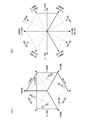
- FIG. 2A is a schematic diagram showing a hexagonal crystal plane
- FIG. 2B is a schematic diagram showing a hexagonal crystal orientation
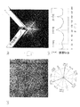
- FIG. 3A is an example (upper diagram) of a digitized X-ray topographic image (basal plane dislocation image) and a schematic diagram of the crystal orientation (lower diagram).
- FIG. 3B is a power spectrum (a spectrum of amplitude A of the Fourier coefficient) obtained by two-dimensional Fourier transform of the digital image of FIG.
- FIG. 3C is a diagram illustrating the angle dependency of the average amplitude. It is a schematic diagram for demonstrating the two-dimensional Fourier transform of an image.
- 4A shows a digital image
- FIG. 4B to 4K show sinusoidal waveforms constituting the digital image of FIG. 4A.
- FIG. 5A is a power spectrum obtained by Fourier transform
- FIG. 5B is an example of a sine waveform at each point.
- FIG. 6A is a cross-sectional view of a SiC seed crystal.
- FIG. 6B is a cross-sectional view of a SiC single crystal grown using the SiC seed crystal shown in FIG.
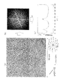
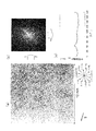
- FIG. 7A is an image (( ⁇ 1010) plane diffraction) of a measurement area of 10 mm square extracted from the center of the X-ray topographic image of the single crystal obtained in Example 1.
- FIG. 7B is a power spectrum (a spectrum of the amplitude A of the Fourier coefficient) obtained by Fourier transforming the X-ray topographic image of FIG.
- FIG.7 (c) is a figure which shows the angle (theta) dependence of the average amplitude Aave. Obtained from the power spectrum of FIG.7 (b).
- FIG. 8A is an image ((1-100) plane diffraction) of a 10 mm square measurement region extracted from the center of the X-ray topographic image of the single crystal obtained in Example 1.
- FIG. 8B is a power spectrum obtained by performing Fourier transform on the X-ray topographic image of FIG.
- FIG. 8C is a diagram illustrating the angle ⁇ dependence of the average amplitude A ave. Obtained from the power spectrum of FIG.
- FIG. 9A is an image ((01-10) plane diffraction) of a 10 mm square measurement region extracted from the center of the X-ray topographic image of the single crystal obtained in Example 1.
- FIG. 9B is a power spectrum obtained by Fourier transforming the X-ray topographic image of FIG.
- FIG. 9C is a diagram illustrating the angle ⁇ dependency of the average amplitude A ave. Obtained from the power spectrum of FIG.
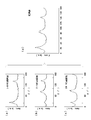
- FIGS. 10 (a) to 10 (c) are diagrams showing the angle ⁇ dependency of the average amplitude A ave. Shown in FIGS. 7 (c), 8 (c), and 9 (c), respectively . is there.
- FIG . 10D shows the integrated value A ′ ave. Of FIGS. 10A to 10C. Integrated value A 'ave. ( ⁇ ) from A' ave. ( ⁇ i) /B.G. Is a diagram showing an example of a method of calculating the (theta i) ratio.
- FIG. 12A shows an X-ray topographic image and orientation intensity in a region away from the facet.
- FIG. 12B shows the X-ray topographic image and the orientation intensity in the region near the facet.
- FIG. 13A is a 10 mm square measurement region image (( ⁇ 1010) plane diffraction) extracted from the X-ray topographic image of the single crystal obtained in Comparative Example 1.
- FIG. 13B is a power spectrum obtained by Fourier transforming the X-ray topographic image of FIG.
- FIG. 13C is a diagram illustrating the angle ⁇ dependency of the average amplitude A ave. Obtained from the power spectrum of FIG. It is a figure which shows the measurement area size dependence of the orientation intensity
- FIG. 6 is a schematic diagram of basal plane dislocations stabilized in the ⁇ 11-20> direction.
- the SiC single crystal according to the present invention has the following configuration.
- the SiC single crystal has high basal plane dislocation linearity, and the basal plane dislocation has at least one orientation region oriented in three crystallographically equivalent ⁇ 11-20> directions.
- the “alignment region” refers to a region determined by the following procedure.
- A) A wafer substantially parallel to the ⁇ 0001 ⁇ plane is cut out from the SiC single crystal.
- Each of the three X-ray topographic images is converted into a digital image in which the luminance of each point in the image is digitized, and each of the three digital images has a side length L of 10 ⁇ 0. Divide into square measuring area of 1 mm.
- D A two-dimensional Fourier transform process is performed on the digital images in the three measurement regions corresponding to the same region on the wafer to obtain a power spectrum (a spectrum of amplitude A of the Fourier coefficient).
- Each of the three power spectra is converted into a polar coordinate function to obtain an angle (direction) -dependent function A ave.
- Oriented region refers to a region in which basal plane dislocations are highly linear and the basal plane dislocations are oriented in three ⁇ 11-20> directions that are crystallographically equivalent. Whether linearity is high and highly oriented can be determined by calculating an A ′ ave. ( ⁇ i ) / BG ( ⁇ i ) ratio from an X-ray topographic image. Details of the determination method will be described later.
- the SiC single crystal only needs to have at least one such orientation region inside.
- an offset substrate is generally used for the seed crystal.
- the c-plane facets In order to suppress the occurrence of heterogeneous polymorphs, it is necessary for the c-plane facets to have screw dislocations that serve to take over the polymorphs of the seed crystal in the growth direction.
- As a method for introducing the screw dislocation into the c-plane facet for example, there is a method of introducing a screw dislocation generation region at the upstream end of the seed crystal.
- an SiC single crystal in which at least one of the orientation regions is in a region excluding facet marks is obtained.
- the region with facet marks corresponds to the screw dislocation generation region and is not originally suitable for device fabrication. For this reason, it is desirable that the alignment region be in a region without facet marks.
- at least one of the orientation regions is located at a substantially central portion of the SiC single crystal. An existing SiC seed crystal is obtained.
- the “substantially central portion of the SiC single crystal” refers to the vicinity of the center of the surface of the wafer cut from the SiC single crystal substantially parallel to the ⁇ 0001 ⁇ plane.
- the orientation region is in the substantially central portion of the single crystal.
- a SiC single crystal having a higher orientation strength B can be obtained as the distance from the facet mark increases. Specifically, “the farther away from the facet mark, the higher the orientation strength B” is.
- the SiC single crystal includes a first alignment region whose distance to the facet mark is L 1 and a second alignment region whose distance to the facet mark is L 2 (> L 1 ).
- “Distance between facet mark and alignment region (L 1 , L 2 )” means the center and orientation of the facet mark appearing on the surface of the wafer when the wafer is cut from the SiC single crystal substantially parallel to the ⁇ 0001 ⁇ plane. The distance connecting the center of the area.
- the region with facet marks corresponds to the screw dislocation generation region and is not originally suitable for device fabrication. Therefore, it is desirable that the alignment region be in a region away from the facet mark. Further, by bringing one of the ⁇ 11-20> directions closer to the offset direction, the orientation and linearity of the basal plane dislocation in the ⁇ 11-20> direction can be improved.
- Area ratio (%) of alignment region means the total area of the alignment region (S 0 ) with respect to the total area (S 0 ) of the measurement region included in the wafer cut from the SiC single crystal substantially parallel to the ⁇ 0001 ⁇ plane.
- the area ratio of the alignment region is preferably 50% or more.
- the area ratio of the alignment region is more preferably 70% or more, and still more preferably 90% or more.
- a SiC single crystal including a relatively large amount of orientation regions can be obtained. Further, when one or more wafers are cut out from the SiC single crystal, an SiC single crystal in which the area ratio of the orientation region of at least one wafer is 50% or more is obtained.
- the higher the alignment strength B of the alignment region the better.
- the orientation strength B is more preferably 1.3 or more, further preferably 1.4 or more, and more preferably 1.5 or more.
- the larger the area ratio of the alignment region having such a high alignment strength B the better.
- Stacking fault Does not include stacking faults” means that an X-ray topographic image corresponding to ⁇ 1-100 ⁇ plane diffraction does not include a plane defect region projected in a planar shape.
- the stacking fault density immediately after manufacturing is low because the stacking fault included in the screw dislocation generation region hardly flows out toward the downstream side in the offset direction.
- the basal plane dislocations hardly flow out, and the conversion of the stacking fault ends into the screw dislocations does not occur.
- the basal plane dislocations are highly oriented, in other words, the curved basal plane dislocations are reduced, and the generation of stacking faults due to the decomposition of the curved basal plane dislocations is also suppressed.
- the “alignment region” is determined by the following procedure.
- Procedure (a) First, a wafer substantially parallel to the ⁇ 0001 ⁇ plane is cut out from the SiC single crystal.
- general sample processing is performed for imaging basal plane dislocations ( ⁇ 0001 ⁇ in-plane dislocations) by X-ray topography.
- the processing is performed under the following conditions. That is, the SiC single crystal is sliced substantially parallel to the ⁇ 0001 ⁇ plane, and a wafer having an offset angle of 10 ° or less is cut out.
- the wafer surface is flattened by grinding and polishing, and the damaged layer on the surface is removed to obtain a wafer having a thickness suitable for X-ray topography measurement.
- a CMP process For the removal of the damaged layer, it is preferable to use a CMP process. If the thickness of the wafer is too thin, the region in the thickness direction to be measured becomes local, so that an average dislocation structure in the crystal cannot be evaluated, and variations in measured values of orientation strength tend to occur. On the other hand, if the wafer is too thick, it is difficult to transmit X-rays. Accordingly, the thickness of the wafer is preferably 100 to 1000 ⁇ m, more preferably 500 ⁇ 200 ⁇ m, and further preferably 500 ⁇ 100 ⁇ m.
- the Lang method is a technique that can image defect distribution of the entire wafer and can be used for quality inspection of the wafer.
- the Lang method includes a method using a large synchrotron radiation facility and a method using a small laboratory-level X-ray generator, and the measurement described in the present invention is possible by using either method.
- a general method for the latter will be described.
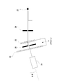
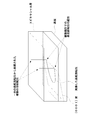
- X-rays emitted from the X-ray source 22 are directed by the first slit 24 and are incident on the sample 26 with a limited width. Incident X-rays are applied to the band-like region of the sample 26.
- the in-plane orientation and the incident angle are adjusted so that the diffraction condition is satisfied with respect to the crystal lattice plane, diffraction occurs in the entire irradiation area.
- the X-ray source 22 an X-ray tube whose anode is Mo is used, and the diffraction condition is adjusted to the wavelength of K ⁇ 1 among the K ⁇ rays of characteristic X-rays.
- the second slit 28 has a function of blocking the primary X-ray transmitted through the sample 26 and reducing the background appropriately so as to allow only the diffracted X-ray to pass through and reducing the background caused by the scattered X-ray.
- a film (or nuclear dry plate) 30 is disposed on the back side of the second slit 28, and an X-ray detector 32 is disposed on the back side thereof.
- a diffraction image over the entire sample 26 can be obtained.
- the topograph obtained in this way is called a traburst graph. Since a three-dimensional defect image is projected two-dimensionally, it is sometimes called a projection topograph.
- ⁇ 11-20 ⁇ plane diffraction As a method for detecting a dislocation having a Burgers vector in the ⁇ 0001 ⁇ in-plane direction, ⁇ 11-20 ⁇ plane diffraction is also generally used. However, stacking faults in the ⁇ 0001 ⁇ plane cannot be detected by ⁇ 11-20 ⁇ plane diffraction. On the other hand, in ⁇ 11-20 ⁇ plane diffraction, dislocations having Burgers vectors in the three principal axes in the ⁇ 0001 ⁇ plane can be detected even with one measurement plane, whereas in ⁇ 1-100 ⁇ plane diffraction, In one measurement plane, only dislocations having Burgers vectors in two principal axis directions out of three principal axis directions can be detected. Therefore, in the present invention, ⁇ 1-100 ⁇ plane diffraction, which can also detect stacking faults, is used to measure three crystal planes having different crystallographically equivalent angles.
- the topographic image obtained on a film or nuclear plate is digitized by a scanner or the like.
- the capture conditions for digitization are shown below.
- a digitized topographic image (digital image) is partitioned into square measurement areas having a side length L of 10 ⁇ 0.1 mm. When the wafer is relatively large, the wafer surface is partitioned into squares and a plurality of measurement areas are taken out. In general, if the measurement region is too small, the measurement becomes local, and a result for the average structure of dislocations in the crystal cannot be obtained.
- the gradation level of the digital image is adjusted so that a clear basal plane dislocation image can be obtained. Specifically, the basal plane dislocation is adjusted to be darkest (black) and the portion without dislocation is adjusted to be brightest (white). (5) The number of pixels on one side is adjusted to 512 pixels. If the number of pixels is too low, a clear basal plane dislocation image cannot be obtained. On the other hand, when there are too many pixels, a Fourier-transform process will become slow.
- each of the three power spectra is converted into a polar coordinate function to obtain an angle (direction) -dependent function A ave. ( ⁇ ) of the average amplitude A (0 ° ⁇ ⁇ ⁇ 180 °) (procedure (e)).
- a ave. ( ⁇ ) of the average amplitude A (0 ° ⁇ ⁇ ⁇ 180 °) (procedure (e)).
- the average amplitude A with respect to the counterclockwise angle ⁇ is calculated with the X-axis direction set to 0 °.
- FIG. 3A shows an example of a digitized X-ray topographic image (basal plane dislocation image).
- This digital image is subjected to two-dimensional Fourier transform to obtain a power spectrum (FIG. 3B).
- the average value of the amplitude is obtained for a certain angle (direction of periodicity), and the function A ave. ( ⁇ ) depending on the angle (direction) of the average amplitude is obtained (FIG. 3C).
- This processing is performed for the basal plane dislocation images obtained under the three diffraction conditions, respectively, and the obtained angular dependence functions A ave. ( ⁇ ) of the three average amplitudes are integrated.
- ⁇ 1-100> in the three theta i corresponding to the direction (i 1 ⁇ 3), when each showing a distinct peak, the area on the wafer corresponding to the measurement region Is determined as an “alignment region”.
- a peak appears in a direction perpendicular to the actual orientation direction.
- the direction perpendicular to the ⁇ 11-20> direction is the ⁇ 1-100> direction (FIG. 2B).
- the appearance of a peak in the ⁇ 1-100> direction by Fourier transform indicates that the basal plane dislocation is oriented in the ⁇ 11-20> direction.
- Waves such as sound waves, electromagnetic waves, and seismic waves can be represented by combinations of trigonometric waves (sin, cos) having different magnitude (amplitude), frequency, and phase.
- the image (FIG. 4 (a)) is also an overlay of trigonometric waves (FIG. 4 (b) to FIG. 4 (k)) having periodicity in various directions and various frequencies.
- a Fourier transform such as a sound wave is to obtain a Fourier coefficient having phase and amplitude information of a trigonometric wave having a certain frequency.
- the Fourier transform of an image means that when the image is a function in two-dimensional coordinates of luminance, (A) periodicity in a certain direction in two-dimensional coordinates, and (B) a Fourier coefficient having phase and amplitude information of a trigonometric wave of a certain frequency, It is to seek.
- a Fourier transform F (k x , k y ) for an image f (x, y) having a size of N ⁇ N pixels is expressed by the following equation (1).
- f is the luminance at the coordinates (x, y), and is obtained by converting a digital image into a bitmap and extracting information on the luminance of each point from the image data.
- k is a frequency.
- the angle formed by the line connecting the origin and a + ib and the real axis means the phase of a trigonometric function having a frequency in the direction of coordinates (x, y) from the center of the image.
- ⁇ (a 2 + b 2 ) that is the distance from the origin to a + ib represents the amplitude A of the trigonometric function wave.
- each coordinate shows a rough periodicity with a longer wavelength as it is closer to the center.
- similar to a side means presence of fine periodicity with a short wavelength.
- the quotient obtained by dividing the length of one side of the image by the distance from the center is the wavelength of the periodicity.
- the direction from the origin to the coordinates means the direction in which this periodicity is repeated.
- the luminance of each coordinate represents the amplitude of the trigonometric function wave.
- a clear spot appears, and the contribution of a specific frequency in a specific periodicity direction can be detected significantly.
- the two-dimensional Fourier transform can be applied not only to images with regularity but also to examining the orientation of fibers, etc. The strength can be examined (see References 1 to 3).
- a clear spot at a certain distance from the center, but a blurred intensity distribution that is anisotropically flattened from the center of the spectrum is observed. If the orientation of the fibers in the image is small, an isotropic power spectrum is obtained.
- the uniaxial orientation is strong, an ellipse or a peak that is greatly flattened in the direction orthogonal to the orientation direction appears in the power spectrum.
- the amplitude A at each coordinate of the power spectrum is represented by a polar coordinate function A ( ⁇ , r) (FIG. 3B).
- ⁇ is an angle formed by a line connecting the center of the spectrum and its coordinates and a horizontal line.
- R represents the distance from the center of the spectrum to its coordinates.
- a ( ⁇ , r) is averaged over all r with respect to a certain constant ⁇ , and the ⁇ dependency A ave. ( ⁇ ) of the average amplitude is obtained.
- ⁇ is in the range of 0 ° to 180 °. This is because 180 ° to 360 ° has the same property as 0 ° to 180 °.
- a ave. ( ⁇ ) As a method for obtaining the strength of the orientation, when A ave. ( ⁇ ) is drawn as a polar graph, the curve is approximated to an ellipse, and the ratio of the major axis to the minor axis is obtained (reference documents 1 to 3). However, in the Fourier transform of the basal plane dislocation image obtained in the present invention, A ave. ( ⁇ ) shows a relatively sharp maximum value and is not uniaxially oriented. Elliptic approximation is not applicable.
- the orientation of the basal plane dislocation is evaluated by taking the following special procedure for A ave. ( ⁇ ) obtained by the two-dimensional Fourier transform.
- a ave. ( ⁇ ) obtained by the two-dimensional Fourier transform.
- Three A ave. ( ⁇ ) corresponding to ⁇ 1-100 ⁇ plane diffraction are obtained from the X-ray topographic image.
- An integrated value A ′ ave. ( ⁇ ) of three A ave. ( ⁇ ) obtained by Fourier transform is obtained.
- any software may be used as long as the same process can be performed.
- this software developed for evaluating the orientation is characterized in that A ave. ( ⁇ ) can be obtained. If A ave. ( ⁇ ) cannot be made automatically by other software, use the power spectrum obtained by mapping the luminance to the (x, y) coordinates, and use the same equation (2). It is necessary to calculate.
- the SiC single crystal according to the present invention can be manufactured by various methods. For example, it can be manufactured by growing a new crystal on the surface of the SiC seed crystal using an SiC seed crystal that satisfies the following conditions. .
- the SiC seed crystal has a main growth surface composed of a plurality of sub-growth surfaces.
- the sub-growth surfaces existing from the uppermost part of the ⁇ 0001 ⁇ plane toward the outer periphery are sequentially formed as a first sub-growth surface, a second sub-growth surface,. If the surface (n ⁇ 2), between the offset angle theta k + 1 of the offset angle theta k and (k + 1) th sub-growth surface of the k sub-growth surface (1 ⁇ k ⁇ n-1 ), ⁇ The relationship k ⁇ k + 1 holds.
- the “main growth surface” refers to a surface of the exposed surface of the SiC seed crystal whose normal vector a has a crucible center axis material direction component.
- the “crucible central axis raw material direction” refers to a direction from the SiC seed crystal toward the raw material and parallel to the central axis of the crucible.
- the “crucible center axis raw material direction” represents a macroscopic growth direction of the SiC single crystal, and is usually a direction perpendicular to the bottom surface of the SiC seed crystal or the bottom surface of the seed crystal base that fixes the SiC seed crystal.
- “Sub-growth surface” refers to individual surfaces constituting the main growth surface.
- the sub-growth surface may be a flat surface or a curved surface.
- Offset angle ⁇ refers to an angle formed by the normal vector a of the sub-growth surface and the normal vector p of the ⁇ 0001 ⁇ plane of the SiC seed crystal.
- ⁇ 0001 ⁇ plane inclination angle ⁇ refers to an angle formed by the crucible center axis raw material direction vector q and the ⁇ 0001 ⁇ plane normal vector p of the SiC seed crystal.
- the “sub-growth surface inclination angle ⁇ ” refers to an angle formed by the crucible center axis raw material direction vector q and the normal vector a of the sub-growth surface.
- the “downstream side in the offset direction” refers to the side opposite to the direction in which the tip of the vector b obtained by projecting the normal vector p of the ⁇ 0001 ⁇ plane onto the sub-growth surface is facing.
- FIG. 6A shows an example of a cross-sectional view of a SiC seed crystal that satisfies the above-described conditions.
- FIG. 6B shows a cross-sectional view of an SiC single crystal manufactured using the SiC seed crystal 12b.
- the SiC seed crystal 12b has a rectangular cross section, and two inclined surfaces X 2 X 3 and X 3 X 4 having different inclination angles are provided at the upper left corner.
- the SiC seed crystal 12b is a so-called offset substrate in which the ⁇ 0001 ⁇ plane inclination angle ⁇ > 0. ⁇ 0001 ⁇ plane uppermost part is a three point X.
- the sub-growth plane inclination angle ⁇ 1 of the X 3 X 4 plane satisfies ⁇ 1 ⁇ ⁇ . Further, the sub-growth plane inclination angle ⁇ 2 of the X 4 X 5 plane is zero.
- X 5 points, among the main growth surface peripheral, at the same time as the distance from X 3 points is the longest point is also a ⁇ 0001 ⁇ plane lowermost portion.
- the normal vectors of the X 1 X 2 plane and the X 5 X 6 plane are perpendicular to the vector q, respectively.
- the X 1 X 6 plane is a plane in contact with a crucible or a seed crystal pedestal (not shown). Therefore, the main growth plane is X 2 X 3 plane + X 3 X 4 + X 4 X 5 plane.
- the direction from the ⁇ 0001 ⁇ plane uppermost portion X 3 point to the X 5 point on the outer periphery of the main growth surface is a direction having a plurality of sub-growth surfaces (main direction).
- the sub-growth surface including the uppermost portion of the ⁇ 0001 ⁇ plane is the X 3 X 4 plane, which becomes the first sub-growth surface.
- the second sub-growth surface is an X 4 X 5 surface, and ⁇ 1 ⁇ 2 is satisfied.
- the SiC seed crystal 12b contains almost no screw dislocations.
- an SiC single crystal that does not include a screw dislocation is obtained by growing using a seed crystal having a growth surface substantially perpendicular to the ⁇ 0001 ⁇ plane. Therefore, a screw dislocation generation region (indicated by a thick line in FIG. 6A) is formed on the surfaces of the X 2 X 3 plane and the X 3 X 4 plane.
- the screw dislocation generation region is (1) After performing one or more a-plane growths using a SiC seed crystal containing screw dislocations, a growth plane is formed on a plane substantially perpendicular to the c-axis so that a region containing screw dislocations remains on the growth surface.
- the offset angle ⁇ 1 it is possible to almost completely suppress the leakage to the downstream side in the offset direction in the growth crystal of the screw dislocation or the edge dislocation in the basal plane.
- the offset angle ⁇ 2 of the second sub-growth surface (X 4 X 5 surface) is relatively large, the screw dislocations in the seed crystal exposed on the second sub-growth surface are directly inherited by the grown crystal. The probability of being reduced becomes easier to convert to basal plane edge dislocations. Basal plane edge dislocation has a property of easily as it flows to the downstream side of the offset direction (X 5 points side). As a result, the screw dislocation density in the grown crystal on the second sub-growth surface can be reduced. Moreover, it becomes easy to suppress generation
- the SiC seed crystal 12b is provided with inclined surfaces X 2 X 3 and X 3 X 4 so that the ⁇ 0001 ⁇ plane uppermost portion X 3 is inside the main growth surface. Therefore, when grown using this, as shown in FIG. 6B, even if the grown crystal expands in the radial direction, there is little possibility that the c-plane facet will deviate from the high-density screw dislocation region. As a result, it is possible to suppress the occurrence of heterogeneous polymorphism resulting from a temporary decrease in the screw dislocation density.
- the SiC seed crystal 12b having such a shape is cut out from a single crystal grown using a plane substantially perpendicular to the c-plane as a growth plane, and the SiC single crystal is grown using this, the base remaining in the grown crystal is obtained.
- the plane dislocation tends to be oriented in the ⁇ 11-20> direction.
- a SiC single crystal including a region substantially free from stacking faults can be obtained. This is because the seed crystal itself has few dislocations that are the source of basal plane dislocations, and there are few screw dislocations that are converted into stacking faults, and there is almost no leakage of screw dislocations from the screw dislocation generation region formed at the seed crystal edge. This is probably because entanglement between the basal plane dislocation and the screw dislocation hardly occurs.
- SiC wafer The SiC wafer which concerns on this invention consists of what was cut out substantially parallel to the ⁇ 0001 ⁇ surface from the SiC single crystal which concerns on this invention.
- the surface of the wafer does not need to be completely parallel to the ⁇ 0001 ⁇ plane, and may be slightly inclined from the ⁇ 0001 ⁇ plane.
- the allowable degree of inclination (offset angle) varies depending on the use of the wafer, but is usually about 0 to 10 °.
- the obtained wafer can be used for various purposes as it is or with a thin film formed on the surface.
- a semiconductor device is manufactured using a wafer
- an epitaxial film is formed on the wafer surface.
- the epitaxial film include nitrides such as SiC and GaN.
- the semiconductor device according to the present invention is manufactured using the SiC wafer according to the present invention. Specifically, as a semiconductor device, (A) LED, (B) Power device diodes and transistors, and so on.
- Example 1 From the SiC single crystal grown with a plane substantially perpendicular to the c-plane as a growth plane, a seed crystal having a plane substantially perpendicular to both the previous growth plane and the c-plane as a growth plane is taken out and grown again using this. Repeated that. A c-plane offset substrate was taken out from the obtained SiC single crystal and processed into the shape shown in FIG. On the X 2 X 3 plane and X 3 X 4 plane on the growth plane, a screw dislocation generation region is formed. Using this, a SiC single crystal was produced by a sublimation reprecipitation method.
- the obtained single crystal was cut substantially parallel to the ⁇ 0001 ⁇ plane (offset angle: 8 °), and surface flattening treatment and damage layer removal treatment were performed to obtain a wafer having a thickness of 500 ⁇ m.
- the damaged layer was removed by CMP treatment.
- X-ray tube Mo target voltage current: 60 kV Voltage / current: 300mA ⁇ 1-100 ⁇ plane diffraction (2 ⁇ : 15.318 °) Second slit width: 2 mm Scanning speed: 2mm / sec Number of scans: 300 times
- FIGS. 7 to 9 show 10 mm square measurement region images extracted from the center of the X-ray topographic image measured for the single crystal obtained in Example 1, and its power spectrum and A ave. ⁇ ).
- 7 corresponds to ( ⁇ 1010) plane diffraction
- FIG. 8 corresponds to (1-100) plane diffraction
- FIG. 9 corresponds to (01-10) plane diffraction.
- the upward direction in the figure is the offset downstream direction, which is a direction inclined several degrees from the [ ⁇ 1010] direction to the [ ⁇ 1 ⁇ 120] direction. 7 to 9, it can be seen that clear streaks are recognized in the direction corresponding to the ⁇ 1-100> direction in the power spectrum.
- FIG. 10D shows the integrated values A ′ ave. ( ⁇ ) of the three A ave. ( ⁇ ) obtained in FIGS. 7 to 9 (FIGS. 10A to 10C).
- FIG. 11 shows an example of a method for calculating the A ′ ave. ( ⁇ i ) /B.G. ( ⁇ i ) ratio from the integrated value A ′ ave. ( ⁇ ).
- FIG. 10D shows that the single crystal obtained in Example 1 shows clear peaks at three ⁇ s corresponding to the ⁇ 1-100> direction. As shown in FIG. 11, at ⁇ i corresponding to the [ ⁇ 1100] direction, the ratio A ′ ave. ( ⁇ i ) /B.G. ( ⁇ i ) was 1.82.
- the ratio A ′ ave. ( ⁇ i ) /B.G. ( ⁇ i ) was 1.54. Further, at ⁇ i corresponding to the [0-110] direction, the ratio A ′ ave. ( ⁇ i ) /B.G. ( ⁇ i ) was 1.43. From these results, it was found that basal plane dislocations were oriented in three ⁇ 11-20> directions. Furthermore, the orientation strength B, which is the average of these, was 1.60. Further, the peak due to the basal plane dislocation in the [ ⁇ 1-120] direction, which is the ⁇ 11-20> direction with the smallest angle with the offset downstream direction, was the largest.
- FIG. 12A shows an X-ray topographic image and an orientation intensity in a region away from the facet.
- FIG. 12B shows an X-ray topographic image and orientation strength in a region near the facet. From FIG. 12, it can be seen that the linearity and orientation of basal plane dislocations are reduced in the vicinity of the facets.
- the screw dislocation generation region is formed up to the X 2 X 3 plane and a certain portion from X 3 to the offset downstream side (portion corresponding to X 4 in FIG. 6A).
- An SiC single crystal was manufactured using this c-plane offset substrate.
- the X-ray topograph of the crystal described in Non-Patent Document 5 is an X-ray topographic image that the present inventor was able to obtain, and has the highest orientation and linearity of the basal plane dislocation image. Are considered to be of high quality.
- a wafer was produced from the obtained single crystal according to the same procedure as in Example 1. [2. Test method] According to the same procedure as in Example 1, A ′ ave. ( ⁇ i ) /B.G. ( ⁇ i ) ratio and orientation strength B at three ⁇ i corresponding to the ⁇ 1-100> direction were determined. .
- FIG. 13 shows an image of a measurement area of 10 mm square in a portion where the orientation strength of the basal plane dislocation is the highest value among the X-ray topographic images measured for the single crystal obtained in Comparative Example 1. , And its power spectrum and A ave. ( ⁇ ). Note that FIG. 13 corresponds to ( ⁇ 1010) plane diffraction. As shown in FIG. 13B, in the power spectrum, no clear streak was observed in the direction corresponding to the ⁇ 1-100> direction.
- a peak was shown in i .
- the ( ⁇ i ) ratio was relatively small.
- no clear peak was shown at ⁇ i corresponding to the [ ⁇ 1010] direction.
- the ratio A ′ ave. ( ⁇ i ) /B.G. ( ⁇ i ) was 1.18.
- the ratio A ′ ave. ( ⁇ i ) /B.G. ( ⁇ i ) was 1.03. Further, at ⁇ i corresponding to the [0-110] direction, the ratio A ′ ave. ( ⁇ i ) /B.G. ( ⁇ i ) was 1.27. From these results, it was found that the orientation of basal plane dislocations in the ⁇ 11-20> direction was low. Furthermore, the orientation strength B, which is the average of these, was 1.16.
- the A ′ ave. ( ⁇ i ) /B.G. ( ⁇ i ) ratio decreased as the measurement area increased.
- the orientation strengths in the other divided regions were all smaller than these when the sizes of the measurement regions were unified and compared.
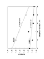
- FIG. 14 shows the measurement region size dependence of the orientation strength B of the single crystals obtained in Example 1 and Comparative Example 1.
- the orientation strength B in the size of each measurement region is plotted. It was found that the relationship between L and B can be approximated by a straight line.
- the reason why the orientation strength B decreases as the measurement region increases is considered to be that the basal plane dislocations in the X-ray topographic image become blurred as the measurement region increases.
- the SiC single crystal according to the present invention can be used as a semiconductor material for an ultra-low power loss power device.
Landscapes
- Chemical & Material Sciences (AREA)
- Engineering & Computer Science (AREA)
- Crystallography & Structural Chemistry (AREA)
- Materials Engineering (AREA)
- Metallurgy (AREA)
- Organic Chemistry (AREA)
- Inorganic Chemistry (AREA)
- Crystals, And After-Treatments Of Crystals (AREA)
- Analysing Materials By The Use Of Radiation (AREA)
Abstract
Description
従来より、α型SiC単結晶を得る方法として、c面成長法が知られている。ここで、「c面成長法」とは、c面又はc面に対するオフセット角が所定の範囲にある面を成長面として露出させたSiC単結晶を種結晶に用いて、昇華再析出法などの方法により成長面上にSiC単結晶を成長させる方法をいう。
また、基底面転位が湾曲している場合、基底面転位が結晶学的に様々な方向を向くことになる。そのような単結晶を用いてデバイスを作製し、デバイスを作動させると、作動中に基底面転位が結晶学的に安定な方向(<11-20>方向)に向いた部分転位に分解することで積層欠陥が形成され(図16参照)、デバイスの特性劣化(バイポーラデバイスの順方向劣化現象)を引き起こすこともある(非特許文献4)。
(1)前記SiC単結晶は、基底面転位の直線性が高く、前記基底面転位が結晶学的に等価な3つの<11-20>方向に配向している少なくとも1以上の配向領域を有する。
(2)前記「配向領域」とは、以下の手順により判定される領域をいう。
(a)前記SiC単結晶から、{0001}面に略平行なウェハを切り出す。
(b)前記ウェハに対して透過配置によるX線トポグラフ測定を行い、結晶学的に等価な3つの{1-100}面回折に対応するX線トポグラフ像を撮影する。
(c)3つの前記X線トポグラフ像を、それぞれ、画像内の各点の輝度を数値化したデジタル画像に変換し、3つの前記デジタル画像を、それぞれ、1辺の長さLが10±0.1mmである正方形の測定領域に区画する。
(d)ウェハ上の同一領域に対応する3つの前記測定領域中の前記デジタル画像に対して2次元フーリエ変換処理を行い、パワースペクトル(フーリエ係数の振幅Aのスペクトル)を得る。
(e)3つの前記パワースペクトルを、それぞれ極座標関数化し、平均振幅Aの角度(方向)依存性の関数Aave.(θ)を求める(0°≦θ≦180°)。
(f)3つの前記Aave.(θ)の積算値A'ave.(θ)をグラフ化(x軸:θ、y軸:A'ave.)し、3つの前記<1-100>方向に相当する3つのθi(i=1~3)において、それぞれ、バックグラウンドB.G.(θi)に対するピーク値A'ave.(θi)の比(=A'ave.(θi)/B.G.(θi)比)を算出する。
(g)3つの前記A'ave.(θi)/B.G.(θi)比がすべて1.1以上であるときは、3つの前記測定領域に対応する前記ウェハ上の領域を「配向領域」と判定する。
さらに、本発明に係る半導体デバイスは、本発明に係るSiCウェハを用いて製造されたものからなる。
このようなSiC単結晶から{0001}面に略平行にウェハを切り出すと、ウェハ表面に露出する基底面転位の数が相対的に少なくなる。そのため、このようなウェハを種結晶に用いてSiC単結晶を成長させ、あるいは、ウェハ表面にエピタキシャル膜を成膜しても、成長結晶又はエピタキシャル膜に承継される転位の数も少なくなる。
また、このようなSiC単結晶を用いて半導体デバイスを作製すると、湾曲した基底面転位が使用中に分解することによる積層欠陥の形成、及び、これに起因するデバイス特性の劣化を抑制することができる。
[1. SiC単結晶]
本発明に係るSiC単結晶は、以下の構成を備えている。
(1)前記SiC単結晶は、基底面転位の直線性が高く、前記基底面転位が結晶学的に等価な3つの<11-20>方向に配向している少なくとも1以上の配向領域を有する。
(2)前記「配向領域」とは、以下の手順により判定される領域をいう。
(a)前記SiC単結晶から、{0001}面に略平行なウェハを切り出す。
(b)前記ウェハに対して透過配置によるX線トポグラフ測定を行い、結晶学的に等価な3つの{1-100}面回折に対応するX線トポグラフ像を撮影する。
(c)3つの前記X線トポグラフ像を、それぞれ、画像内の各点の輝度を数値化したデジタル画像に変換し、3つの前記デジタル画像を、それぞれ、1辺の長さLが10±0.1mmである正方形の測定領域に区画する。
(d)ウェハ上の同一領域に対応する3つの前記測定領域中の前記デジタル画像に対して2次元フーリエ変換処理を行い、パワースペクトル(フーリエ係数の振幅Aのスペクトル)を得る。
(e)3つの前記パワースペクトルを、それぞれ極座標関数化し、平均振幅Aの角度(方向)依存性の関数Aave.(θ)を求める(0°≦θ≦180°)。
(f)3つの前記Aave.(θ)の積算値A'ave.(θ)をグラフ化(x軸:θ、y軸:A'ave.)し、3つの前記<1-100>方向に相当する3つのθi(i=1~3)において、それぞれ、バックグラウンドB.G.(θi)に対するピーク値A'ave.(θi)の比(=A'ave.(θi)/B.G.(θi)比)を算出する。
(g)3つの前記A'ave.(θi)/B.G.(θi)比がすべて1.1以上であるときは、3つの前記測定領域に対応する前記ウェハ上の領域を「配向領域」と判定する。
「配向領域」とは、基底面転位の直線性が高く、基底面転位が結晶学的に等価な3つの<11-20>方向に配向している領域をいう。直線性が高く、高度に配向しているか否かは、X線トポグラフ像からA'ave.(θi)/BG(θi)比を算出することにより判定することができる。判定方法の詳細は、後述する。SiC単結晶は、その内部にこのような配向領域を少なくとも1つ有していればよい。
このような種結晶を用いてc面成長させると、成長結晶のオフセット方向上流側には、窒素の取り込み量が相対的に高いことによる色の濃いc面ファセットの痕跡(ファセット痕)が残る。また、成長に伴い、種結晶中の螺旋転位発生領域に含まれる積層欠陥や基底面転位が成長結晶に引き継がれ、オフセット方向の下流側に向かって流れ出すことで、螺旋転位や基底面転位の密度が高くなる。そのため、従来のc面成長法では、ファセット痕から離れた領域においても基底面転位が湾曲しやすくなり、配向性が低下する。
また、後述する方法を用いてSiC単結晶を製造する場合において、c面ファセットが端部にあるオフセット基板を種結晶に用いたときには、配向領域の少なくとも1つが、SiC単結晶の略中央部に存在するSiC種結晶が得られる。ここで、「SiC単結晶の略中央部」とは、SiC単結晶から{0001}面に略平行に切り出されたウェハの表面の中心近傍をいう。通常、デバイスは、ウェハの端部を除く領域に作製されるため、単結晶の略中央部に配向領域があるのが望ましい。
「ファセット痕から遠ざかるほど、配向強度Bが高い」とは、具体的には、
(1)SiC単結晶は、ファセット痕までの距離がL1である第1の配向領域と、ファセット痕までの距離がL2(>L1)である第2の配向領域とを備えており、
(2)第2の配向領域に対応する配向強度B(=3つのA'ave.(θi)/B.G.(θi)比の平均値)が、第1の配向領域に対応する前記配向強度Bより大きい
ことをいう。
「ファセット痕と配向領域との距離(L1、L2)」とは、SiC単結晶から{0001}面に略平行にウェハを切り出した時に、ウェハの表面に現れたファセット痕の中心と配向領域の中心とを結ぶ距離をいう。ファセット痕のある領域は、螺旋転位発生領域に対応するため、デバイス作製用として元々適さない。そのため、ファセット痕から離れた領域に配向領域があることが望ましい。また、<11-20>方向の1つをオフセット方向に近づけることで、その<11-20>方向への基底面転位の配向性と直線性を向上させることができる。
「配向領域の面積率(%)」とは、SiC単結晶から{0001}面に略平行に切り出されたウェハに含まれる測定領域の面積の総和(S0)に対する配向領域の面積の総和(S)の割合(=S×100/So)をいう。
SiC単結晶から{0001}面に略平行にウェハを切り出し、切り出されたウェハを用いて高性能な半導体デバイスを高い歩留まりで製造するためには、配向領域の面積率は、高いほど良い。配向領域の面積率は、具体的には、50%以上が好ましい。配向領域の面積率は、さらに好ましくは70%以上、さらに好ましくは90%以上である。
後述する方法を用いると、相対的に多量の配向領域を含むSiC単結晶が得られる。また、製造条件を最適化すると、SiC単結晶から1又は2以上のウェハを切り出したときに、少なくとも1つのウェハの配向領域の面積率が50%以上であるSiC単結晶が得られる。
「配向強度B」とは、結晶学的に等価な3つの<1-100>方向に対応する3つのA'ave.(θi)/B.G.(θi)比(i=1~3)の平均値を言う。配向強度Bが大きいほど、基底面転位の直線性が高く、<11-20>方向への配向性が高いことを示す。
後述する方法を用いた場合において、製造条件を最適化すると、配向強度Bが1.2以上である少なくとも1つの配向領域を含むSiC単結晶が得られる。
SiC単結晶から{0001}面に略平行にウェハを切り出し、切り出されたウェハを用いて高性能な半導体デバイスを高い歩留まりで製造するためには、配向領域の配向強度Bは、大きいほど良い。配向強度Bは、さらに好ましくは1.3以上、さらに好ましくは1.4以上、さらに好ましくは1.5以上である。
同様に、このような高い配向強度Bを持つ配向領域の面積率は、大きいほど良い。
「積層欠陥を含まない」とは、{1-100}面回折に対応するX線トポグラフ像において、面状に投影される面欠陥領域を含まないことをいう。
後述する方法を用いて本発明に係るSiC単結晶を製造すると、螺旋転位発生領域に含まれている積層欠陥がオフセット方向下流側に向かって流れ出しにくいため、製造直後の積層欠陥密度は低い。また、同時に基底面転位も流れ出しにくく、積層欠陥端部の螺旋転位への変換も生じないため、転位同士の相互作用が起きにくくなる。その結果、基底面転位が高度に配向化、言い換えると湾曲した基底面転位が少なくなり、湾曲している基底面転位が分解することによる積層欠陥の生成も抑制される。
「配向領域」は、以下の手順により判定される。
[2.1. 試料の加工:手順(a)]
まず、SiC単結晶から、{0001}面に略平行なウェハを切り出す。
本発明においては、X線トポグラフにより基底面転位({0001}面内転位)を撮影するための、一般的な試料加工を行うことを前提とする。詳細には、下記の条件で加工を施す。
すなわち、SiC単結晶を{0001}面に略平行にスライスし、オフセット角が10°以下のウェハを切り出す。ウェハ表面を研削、研磨により平坦化し、さらに表面のダメージ層を除去し、X線トポグラフの測定に適した厚さのウェハにする。ダメージ層の除去には、CMP処理を用いるのが好ましい。
ウェハの厚さが薄すぎると、測定される厚さ方向の領域が局所的になることで、結晶中の平均的な転位構造を評価できないほか、配向強度の測定値にバラツキが生じやすくなる。一方、ウェハの厚さが厚すぎると、X線を透過させるのが困難となる。従って、ウェハの厚さは、100~1000μmが好ましく、さらに好ましくは、500±200μm、さらに好ましくは、500±100μmである。
次に、ウェハに対して透過配置によるX線トポグラフ測定を行い、結晶学的に等価な3つの{1-100}面回折に対応するX線トポグラフ像を撮影する。
本発明においては、基底面転位像を検出するための一般的なX線トポグラフ測定条件で行うことを前提とする。詳細には、下記の条件で測定する。
配置: 透過配置(Lang法、図1参照)
回折条件と測定面: {1-100}面回折を使用する。主に、{0001}面内方向のバーガースベクトルを有する転位や欠陥の検出を目的とする回折であり、かつ{0001}面内積層欠陥の検出も可能である。結晶の同一の領域を、結晶学的に等価であるが、角度の異なる3つの面の組み合わせで測定する。3つの面とは、(1-100)面、(-1010)面、及び(01-10)面をいう。図2(a)参照。
図1に示すように、X線源22より放射されたX線は第1スリット24により方向付けされ、幅を制限して試料26に入射される。入射X線は、試料26の帯状の領域に照射される。結晶の格子面に対し回折条件を満足するように面内の方位と入射角が調整されると、照射全域で回折を起こす。
X線源22として、陽極がMoのX線管を使用し、特性X線のKα線の内、Kα1の波長に回折条件を合わせる。第2スリット28は、試料26を透過してきた一次X線を遮断するとともに、回折X線だけを通すように、適宜その幅を狭め、散乱X線によるバックグラウンドを低減する働きを持つ。第2スリット28の背面側には、フィルム(又は、原子核乾板)30が配置され、さらにその背面側には、X線検出器32が配置されている。
以上の配置で、試料26をフィルム30と一緒に試料面に平行に走査すると、試料26全体にわたる回折像を得ることができる。
こうして得られたトポグラフをトラバーストポグラフと呼ぶ。3次元的な欠陥像を2次元的に投影するので、プロジェクショントポグラフと呼ぶこともある。
一方、{11-20}面回折では、1つの測定面でも{0001}面内の3つの主軸方向のバーガースベクトルを有する転位を検出可能であるのに対し、{1-100}面回折では、1つの測定面では、3つの主軸方向の内、2つの主軸方向のバーガースベクトルを有する転位しか検出できない。
そこで、本発明では、積層欠陥の検出も可能な{1-100}面回折を用い、これを結晶学的に等価な角度の異なる3つの結晶面に対して測定を行うこととした。
次に、3つの前記X線トポグラフ像を、それぞれ、画像内の各点の輝度を数値化したデジタル画像に変換し、3つの前記デジタル画像を、それぞれ、大きさが10±0.1mmである測定領域に区画する。
本発明においては、画像解析を行うための一般的な処理を行うことを前提とする。詳細には、下記条件でデジタル化及び画像前処理を行う。
解像度: フィルムの実寸法上で、512ピクセル/cm以上とする。
モード: グレースケール
(2)デジタル化したトポグラフ像(デジタル画像)を、1辺の長さLが10±0.1mmである正方形の測定領域に区画する。ウェハが相対的に大きいときには、ウェハ表面をマス目状に区画し、複数個の測定領域を取り出す。一般に、測定領域が小さすぎると、測定が局所的になり、結晶中の転位の平均的な構造に対する結果が得られない。一方、測定領域が大きすぎると、基底面転位像が細くなりすぎて不鮮明になり、配向性を調べることが困難になる。
(4)明瞭な基底面転位像が得られるように、デジタル画像の階調レベルを調整する。具体的には、基底面転位部分を最も暗く(黒)、転位のない部分を最も明るく(白)調整する。
(5)一辺のピクセル数を512ピクセルに調整する。ピクセル数が低すぎると、明確な基底面転位像が得られない。一方、ピクセル数が多すぎると、フーリエ変換処理が遅くなる。
次に、ウェハ上の同一領域に対応する3つの前記測定領域中の前記デジタル画像に対して2次元フーリエ変換処理を行い、パワースペクトル(フーリエ係数の振幅Aのスペクトル)を得る。
2次元フーリエ変換による画像解析の原理については、例えば、
(1) 江前敏晴、”画像処理を用いた上の物性解析法”、紙パルプ技術タイムス、48(11)、1-5(2005)(参考文献1)、
(2) Enomae, T., Han, Y.-H. and Isogai, A., "Fiber orientation distribution of paper surface calculated by image analysis," Proceedings of International Papermaking and Environment Conference, Tianjin, P.R.China(May 12-14), Book2, 355-368(2004)(参考文献2)、
(3) Enomae, T., Han, Y.-H. and Isogai, A., "Nondestructive determination of fiber orientation distribution of fiber surface by image analysis," Nordic Pulp Research Journal 21(2): 253-259(2006)(参考文献3)、
(4) http://www.enomae.com/FiberOri/index.htm(2012年5月現在)(参考URL1)、
などに詳細に記載されている。
次に、3つの前記パワースペクトルを、それぞれ極座標関数化し、平均振幅Aの角度(方向)依存性の関数Aave.(θ)を求める(0°≦θ≦180°)(手順(e))。極座標関数化では、以下の処理を行う。パワースペクトルにおいて、X軸方向を0°として、反時計回りの角度θに対する平均振幅Aを計算する。つまり、θを0~180°の範囲で等分割し、各角度についてパワースペクトルの中心から端部までのフーリエ係数の振幅の平均を求める。
次いで、3つの前記Aave.(θ)の積算値A'ave.(θ)をグラフ化(x軸:θ、y軸:A'ave.)し、3つの前記<1-100>方向に相当する3つのθi(i=1~3)において、それぞれ、バックグラウンドB.G.(θi)に対するピーク値A'ave.(θi)の比(=A'ave.(θi)/B.G.(θi)比)を算出する(手順(f))。このようにして得られた3つの前記A'ave.(θi)/B.G.(θi)比がすべて1.1以上であるときは、3つの前記測定領域に対応する前記ウェハ上の領域を「配向領域」と判定する(手順(g))。
「バックグラウンドB.G.(θi)」とは、θiの位置におけるx軸からバックグランド線までの距離をいう。「バックグランド線」とは、θi近傍における積算値A'ave.(θ)のグラフの下端に接する接線をいう(図11参照)。
フーリエ変換では、現実の配向方向に対して垂直な方向にピークが現れる。SiCなどの六方晶系の結晶構造では、<11-20>方向に垂直な方向は、<1-100>方向となる(図2(b))。すなわち、フーリエ変換により<1-100>方向にピークが現れることは、基底面転位が<11-20>方向に配向していることを表す。また、配向強度B(=3つのA'ave.(θi)/B.G.(θi)比の平均値)が大きいことは、基底面転位の<11-20>方向への配向性が高いことを表す。
音波、電磁波、地震波などの波は、大きさ(振幅)、周波数、及び位相が異なる三角関数波(sin、cos)の組み合わせで表すことができる。同様に、図4に示すように、画像(図4(a))も、種々の方向の周期性と種々の周波数を有する三角関数波(図4(b)~図4(k))の重ね合わせで表現することができる。
音波などのフーリエ変換は、ある周波数の三角関数波の位相と振幅の情報を有するフーリエ係数を求めることである。同様に、画像のフーリエ変換とは、画像を輝度の二次元座標における関数とした際に、
(a)2次元座標におけるある方向の周期性、及び、
(b)ある周波数の三角関数波の、位相と振幅の情報を有するフーリエ係数、
を求めていくことである。

位相の情報を取り除いた振幅A=√(a2+b2)を、周波数の大きさと周期性の方向を意味するマップ上にプロットしたものをパワースペクトル(図5(a))(フーリエ係数の振幅Aのスペクトル)という。パワースペクトル中において、各座標は、中心に近いほど、波長の長い粗い周期性を示す。また、辺に近い周囲部のピークは、波長の短い細かい周期性の存在を意味する。画像の一辺の長さを中心からの距離で割った商が、その周期性の波長になる。また、原点からその座標までの方向は、この周期性が繰り返される方向を意味する。各座標の輝度は、その三角関数波の振幅を表す。
A(θ、r)を、ある一定θに関してすべてのrで平均化し、平均振幅のθ依存性Aave.(θ)を求める。その際、θは、0°~180°の範囲とする。これは、180°~360°は、0°~180°と同じになる性質があるためである。具体的には、2次元フーリエ変換後、0~180°の角度を等分割し、各角度θについて距離rに位置するフーリエ係数の振幅A(rcosθ、rsinθ)を求め、rに関してその平均値Aave.(θ)を求める。これは、(2)式で表される。

(1){0001}面内における、結晶学的に等価で角度の異なる3つの{1-100}面について、{1-100}面回折によるX線トポグラフを行い、3つの基底面転位のX線トポグラフ像を得る。X線トポグラフ像から、{1-100}面回折に対応する3つのAave.(θ)を求める。
(2)フーリエ変換で求めた3つのAave.(θ)の積算値A'ave.(θ)を求める。
(3)積算値A'ave.(θ)をグラフ化した際に、A'ave.(θ)が<1-100>方向に相当する3つのθにおいて、それぞれ明確なピークを示した場合には、基底面転位が<11-20>方向に配向していると判定する。
本発明において、基底面転位像をフーリエ変換するために、参考文献1~3の著者らが開発したFiber Orientation Analysis Ver.8.13を用いた。このフーリエ変換ソフトの処理内容は、画像データから各点の輝度の情報を取り出し、フーリエ変換処理を行い、パワースペクトルとAave.(θ)を求めるものである。詳細な手順は、参考文献1~3及び参考URL1に記載されている。このソフトで画像をフーリエ変換処理するためには、輝度の数値情報を取り出すために画像を予めビットマップ化する。さらに高速フーリエ変換を行うために、画像の一辺のピクセル数が4の整数倍となるように予め調整する。
本発明に係るSiC単結晶は、種々の方法により製造できるが、例えば、以下の条件を満たすSiC種結晶を用いて、SiC種結晶の表面に新たな結晶を成長させることにより製造することができる。
(1)SiC種結晶は、複数個の副成長面からなる主成長面を備えている。
(2)前記SiC種結晶の主成長面上にある{0001}面最上位部から前記主成長面の外周に向かう任意の方向の中に、複数個の前記副成長面を有する方向(主方向)が存在する。
(3)前記主方向に沿って、{0001}面最上位部側から外周に向かって存在する前記副成長面を、順次、第1副成長面、第2副成長面、…第n副成長面(n≧2)とする場合、第k副成長面(1≦k≦n-1)のオフセット角θkと第(k+1)副成長面のオフセット角θk+1との間に、θk<θk+1の関係が成り立つ。
「副成長面」とは、主成長面を構成する個々の面をいう。副成長面は、平面であっても良く、あるいは、曲面であっても良い。
「オフセット角θ」とは、副成長面の法線ベクトルaと、SiC種結晶の{0001}面の法線ベクトルpとのなす角をいう。
「{0001}面傾斜角β」とは、坩堝中心軸原料方向ベクトルqと、SiC種結晶の{0001}面法線ベクトルpとのなす角をいう。
「副成長面傾斜角α」とは、坩堝中心軸原料方向ベクトルqと副成長面の法線ベクトルaとのなす角をいう。
「オフセット方向下流側」とは、{0001}面の法線ベクトルpを副成長面上に投影したベクトルbの先端が向いている向きとは反対向きの側をいう。
図6(a)において、SiC種結晶12bは、断面が矩形で、左上角に傾斜角の異なる2つの傾斜面X2X3、X3X4が設けられている。また、SiC種結晶12bは、{0001}面傾斜角β>0である、いわゆるオフセット基板である。
{0001}面最上位部は、X3点である。X3X4面の副成長面傾斜角α1は、α1≦βになっている。また、X4X5面の副成長面傾斜角α2は、ゼロである。X5点は、主成長面外周の内、X3点からの距離が最も長い点であると同時に、{0001}面最下位部でもある。
SiC種結晶12bは、螺旋転位をほとんど含まない。螺旋転位を含まないSiC単結晶は、例えば特許文献1に記載のように、{0001}面に略垂直な成長面を有する種結晶を用いて、成長させることにより得られる。そのため、X2X3面及びX3X4面の表面には、螺旋転位発生領域(図6(a)中、太線で表示)が形成されている。
螺旋転位発生領域は、
(1)螺旋転位を含むSiC種結晶を用いて、1回以上のa面成長を行った後、螺旋転位を含む領域が成長面上に残るように、c軸とほぼ垂直な面を成長面として露出させる方法(螺旋転位残存法)、
(2)c面から8°傾く面を成長面として露出させたSiC種結晶を切り出し、成長面のオフセット方向の端部に、成長面から10~20°傾く研削面を形成する方法(研削法)、
(3)相対的に高い螺旋転位密度を持つSiC種結晶(高転位密度種結晶)と、相対的に螺旋転位密度が低いSiC種結晶(低転位密度種結晶)とを、成長面が同一面内配置されるように並べる方法(貼り合わせ法)、
(4)種結晶の成長面の一部に、螺旋転位を形成するための後退部(傾斜面、段差、曲面、錐形状のへこみ、くさび形の切り欠きなど)を形成し、後退部上にSiC単結晶を予備成長させる方法(予備成長法)、
などがある(特許第3764462号公報、特開2010-235390号公報参照)。
すなわち、第1副成長面(X3X4面)のオフセット角θ1を相対的に小さくすると、第1副成長面上又はその近傍に露出している種結晶中の螺旋転位は、ほぼ成長結晶に引き継がれる。その結果、第1副成長上又はその近傍にあるc面ファセット内に螺旋転位を確実に供給することができ、これによって、成長結晶中での異種多形や異方位結晶の発生が抑制される。また、オフセット角θ1をより小さくすることで、螺旋転位や基底面内刃状転位の成長結晶におけるオフセット方向下流側への漏れ出しをほぼ完全に抑制できる。
一方、第2副成長面(X4X5面)のオフセット角θ2を相対的に大きくすると、第2副成長面上に露出している種結晶中の螺旋転位は、成長結晶にそのまま引き継がれる確率が小さくなり、基底面刃状転位に変換されやすくなる。基底面刃状転位は、そのままオフセット方向の下流側(X5点側)に流れやすい性質を持つ。その結果、第2副成長面上の成長結晶中の螺旋転位密度を低減することができる。また、新たな螺旋転位の発生を抑制しやすくなる。
本発明に係るSiCウェハは、本発明に係るSiC単結晶から、{0001}面に略平行に切り出されたものからなる。
ウェハの表面は、{0001}面に対して完全に平行である必要はなく、{0001}面から若干傾いていても良い。許容される傾きの程度(オフセット角)は、ウェハの用途により異なるが、通常、0~10°程度である。
本発明に係る半導体デバイスは、本発明に係るSiCウェハを用いて製造されるものからなる。半導体デバイスとしては、具体的には、
(a)LED、
(b)パワーデバイス用のダイオードやトランジスタ、
などがある。
SiC単結晶をc面成長させる場合において、表面のオフセット角が特定の条件を満たす種結晶を用いると、基底面転位の直線性が高く、基底面転位が安定な<11-20>方向に高度に配向したSiC単結晶が得られる。
このようなSiC単結晶から{0001}面に略平行にウェハを切り出すと、ウェハ表面に露出する基底面転位の数が相対的に少なくなる。そのため、このようなウェハを種結晶に用いてSiC単結晶を成長させ、あるいは、ウェハ表面にエピタキシャル膜を成膜しても、成長結晶又はエピタキシャル膜に承継される転位の数も少なくなる。
また、このようなSiC単結晶を用いて半導体デバイスを作製すると、湾曲した基底面転位が使用中に分解することによる積層欠陥の形成、及び、これに起因するデバイス特性の劣化を抑制することができる。
[1. 試料の作製]
c面に略垂直な面を成長面として成長させたSiC単結晶から、直前の成長面及びc面の両方に略垂直な面を成長面とする種結晶を取り出し、これを用いて再び成長することを繰り返した。得られたSiC単結晶からc面オフセット基板を取り出し、図6(a)に示す形状に加工した。成長面上のX2X3面及びX3X4面には、螺旋転位発生領域が形成されている。これを用いて、昇華再析出法によりSiC単結晶を作製した。得られた単結晶を{0001}面に略平行(オフセット角:8°)に切断し、表面の平坦化処理及びダメージ層除去処理を行うことで、厚さ500μmのウェハを得た。ダメージ層は、CMP処理により除去した。
[2.1. X線トポグラフ測定]
結晶学的に等価であり、60°づつ面方位の異なる(-1010)面、(1-100)面、及び(01-10)面の3つの面について、{1-100}面回折像を測定し、感光フィルムにX線トポグラフ像を得た。得られた3つのX線トポグラフ像には、{0001}面内に直線的に伸びる基底面転位像が観察された。
X線トポグラフの測定条件は、以下の通りである。
X線管: Moターゲット
電圧電流: 60kV
電圧電流: 300mA
{1-100}面回折(2θ:15.318°)
第2スリットの幅: 2mm
走査速度: 2mm/sec
走査回数: 300回
これらのX線トポグラフ像をスキャナで取り込むことで、デジタル化した。取り込み条件はグレースケール、解像度は約1000ピクセル/cmとした。デジタル化したX線トポグラフ像の中央部付近から、1辺の長さLが10~20mmである正方形の測定領域を抜き出し、基底面転位部分が最も暗く、無転位部分が最も明るくなるように、階調のレベル補正を行った。画像の一辺のピクセル数が512ピクセルになるように画像の解像度を落とし、ビットマップ形式の画像ファイルに変換した。
前処理を行った3つのデジタル画像を、フーリエ変換ソフトであるFiber Orientation Analysis Ver.8.13を用いて処理し、それぞれパワースペクトルと、Aave.(θ)を求めた。さらに、3つの画像に対して得られたAave.(θ)を積算した。さらに、積算値A'ave.(θ)を用いて、<1-100>方向に相当する3つのθi(i=1~3)におけるA'ave.(θi)/B.G.(θi)比、及び、配向強度Bを求めた。
図7~図9に、それぞれ、実施例1で得られた単結晶について測定されたX線トポグラフ像の中央部から抜き出した10mm角の測定領域の画像、並びに、そのパワースペクトル及びAave.(θ)を示す。なお、図7は(-1010)面回折に、図8は(1-100)面回折に、図9は(01-10)面回折に、それぞれ対応する。図の上方向がオフセット下流方向であり、[-1010]方向から、[-1-120]方向に数度傾いた方向である。図7~図9より、パワースペクトルには、<1-100>方向に相当する方向に明確な筋が認められることがわかる。
図10(d)より、実施例1で得られた単結晶は、<1-100>方向に相当する3つのθにおいて、明確なピークを示すことがわかる。図11に示すように、[-1100]方向に相当するθiでは、A'ave.(θi)/B.G.(θi)比は、1.82であった。[-1010]方向に相当するθiでは、A'ave.(θi)/B.G.(θi)比は、1.54であった。さらに、[0-110]方向に相当するθiでは、A'ave.(θi)/B.G.(θi)比は、1.43であった。これらの結果から、基底面転位は、3つの<11-20>方向に配向していることがわかった。さらに、これらの平均である配向強度Bは、1.60であった。また、オフセット下流方向となす角度が最も小さい<11-20>方向である[-1-120]方向の基底面転位に起因するピークが最大であった。
実施例1の場合、測定領域の大きさによらず、<1-100>方向に相当する3つのθiにおいて、明確なピークを示した。また、測定領域が大きくなるに従い、A'ave.(θi)/B.G.(θi)比が小さくなった。これは、測定領域が大きくなると、相対的に基底面転位が不鮮明になるためである。
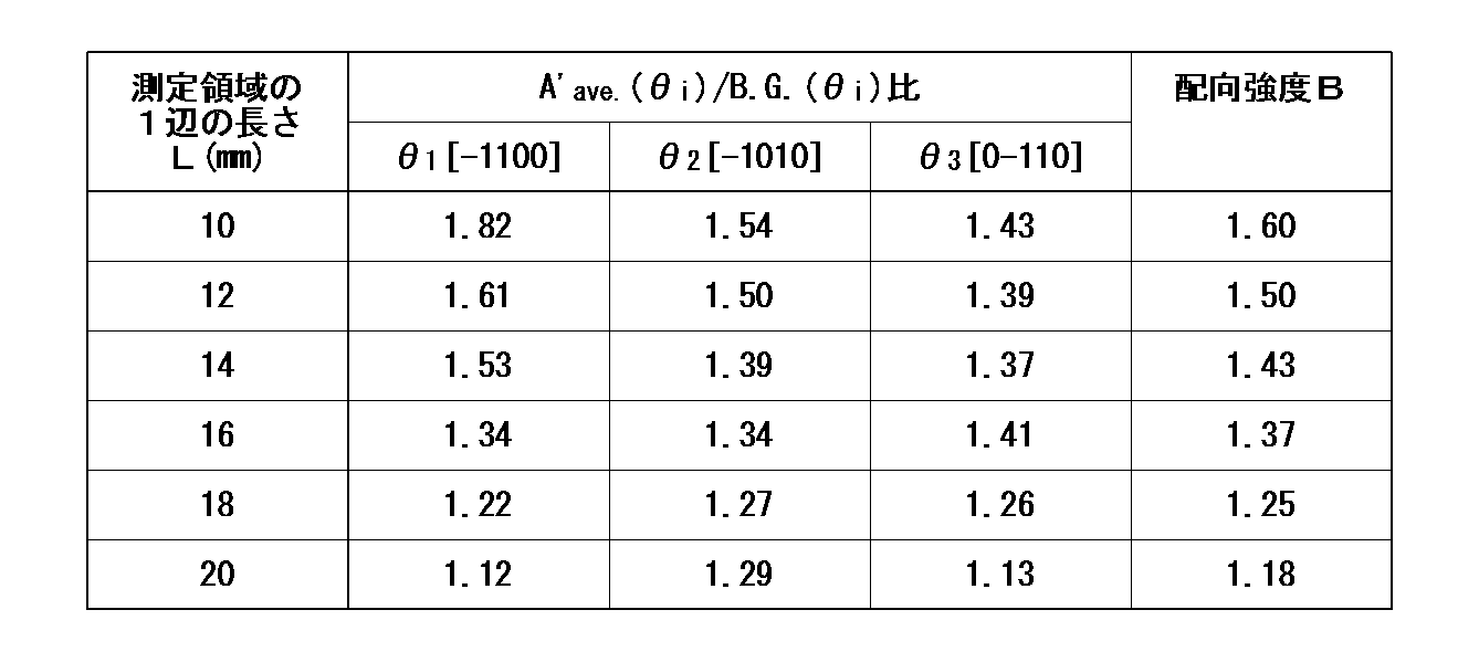
図12(a)に、ファセットから離れた領域でのX線トポグラフ像及び配向強度を示す。また、図12(b)に、ファセット近傍の領域でのX線トポグラフ像及び配向強度を示す。図12より、ファセット近傍においては、基底面転位の直線性及び配向性が低下していることがわかる。
[1. 試料の作製]
c面に略垂直な面を成長面として成長させたSiC単結晶から、直前の成長面及びc面の両方に略垂直な面を成長面とする種結晶を取り出し、これを用いて再び成長することを繰り返した。得られたSiC単結晶からc面オフセット基板を取り出した。なお、図6(a)に示すような加工(X3X4面がX4X5面よりオフセット角が小さくなるような加工)は施さなかった。また、X2X3面及びX3からオフセット下流側への一定部分(図6(a)におけるX4までに相当する部分)まで、螺旋転位発生領域が形成されている。このc面オフセット基板を用いて、SiC単結晶を製造した。なお、非特許文献5に記載された結晶のX線トポグラフは、本願発明者が入手することができたX線トポグラフ像であって、基底面転位像の配向性と直線性が最も高く、結晶が高品質であると考えられるものである。得られた単結晶から、実施例1と同様の手順に従い、ウェハを作製した。
[2. 試験方法]
実施例1と同様の手順に従い、<1-100>方向に相当する3つのθiにおけるA'ave.(θi)/B.G.(θi)比、及び、配向強度Bを求めた。
図13に、比較例1で得られた単結晶について測定されたX線トポグラフ像の中で、結果的に基底面転位の配向強度が最も高い値となった部分における10mm角の測定領域の画像、並びに、そのパワースペクトル及びAave.(θ)を示す。なお、図13は、(-1010)面回折に対応する。図13(b)に示すように、パワースペクトルでは、<1-100>方向に相当する方向には、明確な筋が認められなかった。
比較例1の場合、測定領域の大きさによらず、<1-100>方向に相当する3つθiの内、いずれか1以上のθiにおいて、明確なピークを示さなかった。また、測定領域が大きくなるに従い、A'ave.(θi)/B.G.(θi)比が小さくなった。もちろん、他の区分領域における配向強度は、測定領域の大きさを統一して比較した場合に、いずれもこれらより小さな値となった。

Claims (12)
- 以下の構成を備えたSiC単結晶。
(1)前記SiC単結晶は、基底面転位の直線性が高く、前記基底面転位が結晶学的に等価な3つの<11-20>方向に配向している少なくとも1以上の配向領域を有する。
(2)前記「配向領域」とは、以下の手順により判定される領域をいう。
(a)前記SiC単結晶から、{0001}面に略平行なウェハを切り出す。
(b)前記ウェハに対して透過配置によるX線トポグラフ測定を行い、結晶学的に等価な3つの{1-100}面回折に対応するX線トポグラフ像を撮影する。
(c)3つの前記X線トポグラフ像を、それぞれ、画像内の各点の輝度を数値化したデジタル画像に変換し、3つの前記デジタル画像を、それぞれ、1辺の長さLが10±0.1mmである正方形の測定領域に区画する。
(d)ウェハ上の同一領域に対応する3つの前記測定領域中の前記デジタル画像に対して2次元フーリエ変換処理を行い、パワースペクトル(フーリエ係数の振幅Aのスペクトル)を得る。
(e)3つの前記パワースペクトルを、それぞれ極座標関数化し、平均振幅Aの角度(方向)依存性の関数Aave.(θ)を求める(0°≦θ≦180°)。
(f)3つの前記Aave.(θ)の積算値A'ave.(θ)をグラフ化(x軸:θ、y軸:A'ave.)し、3つの前記<1-100>方向に相当する3つのθi(i=1~3)において、それぞれ、バックグラウンドB.G.(θi)に対するピーク値A'ave.(θi)の比(=A'ave.(θi)/B.G.(θi)比)を算出する。
(g)3つの前記A'ave.(θi)/B.G.(θi)比がすべて1.1以上であるときは、3つの前記測定領域に対応する前記ウェハ上の領域を「配向領域」と判定する。 - 前記配向領域の少なくとも1つは、前記SiC単結晶のファセット痕を除く領域にある請求項1に記載のSiC単結晶。
- 前記配向領域の少なくとも1つは、前記SiC単結晶の略中央部にある請求項1に記載のSiC単結晶。
- 前記SiC単結晶のファセット痕までの距離がL1である第1の配向領域と、
前記ファセット痕までの距離がL2(>L1)である第2の配向領域とを備え、
前記第2の配向領域に対応する配向強度B(=3つの前記A'ave.(θi)/B.G.(θi)比の平均値)は、前記第1の配向領域に対応する前記配向強度Bより大きい
請求項1に記載のSiC単結晶。 - <11-20>方向の内、オフセット下流方向となす角度が最も小さい<11-20>方向への基底面転位の配向を反映するパワースペクトル中の<1-100>方向のピーク値A'ave.(θi)が最も大きい
請求項1に記載のSiC単結晶。 - 前記SiC単結晶から切り出された少なくとも1つの前記ウェハは、前記測定領域の面積の総和(S0)に対する前記配向領域の面積の総和(S)の割合(=S×100/So)が50%以上である
請求項1に記載のSiC単結晶。 - 前記配向領域の少なくとも1つは、配向強度B(=3つの前記A'ave.(θi)/BG(θi)比の平均値)が1.2以上である請求項1に記載のSiC単結晶。
- 積層欠陥を含まない請求項1に記載のSiC単結晶。
- 請求項1に記載のSiC単結晶から、{0001}面に略平行に切り出されたSiCウェハ。
- 表面にエピタキシャル膜が形成されている請求項9に記載のSiCウェハ。
- 請求項9に記載のSiCウェハを用いて製造される半導体デバイス。
- 前記半導体デバイスは、ダイオード、トランジスタ、又は、LEDである請求項11に記載の半導体デバイス。
Priority Applications (5)
| Application Number | Priority Date | Filing Date | Title |
|---|---|---|---|
| US14/110,574 US9166008B2 (en) | 2011-05-16 | 2012-05-16 | SiC single crystal, SiC wafer, and semiconductor device |
| KR1020137033382A KR101713006B1 (ko) | 2011-05-16 | 2012-05-16 | SiC 단결정, SiC 웨이퍼 및 반도체 디바이스 |
| SE1351437A SE1351437A1 (sv) | 2011-05-16 | 2012-05-16 | Enkristall av SiC, SiC skiva, och halvledaranordning |
| CN201280023709.2A CN103635615B (zh) | 2011-05-16 | 2012-05-16 | 碳化硅单晶、碳化硅晶片和半导体器件 |
| DE112012002126.6T DE112012002126B4 (de) | 2011-05-16 | 2012-05-16 | SiC-EINKRISTALL, SiC-WAFER UND UND VERWENDUNG DES SiC-WAFERS ZUR HERSTELLUNG EINER HALBLEITERVORRICHTUNG |
Applications Claiming Priority (2)
| Application Number | Priority Date | Filing Date | Title |
|---|---|---|---|
| JP2011109773A JP6025306B2 (ja) | 2011-05-16 | 2011-05-16 | SiC単結晶、SiCウェハ及び半導体デバイス |
| JP2011-109773 | 2011-05-16 |
Publications (1)
| Publication Number | Publication Date |
|---|---|
| WO2012157654A1 true WO2012157654A1 (ja) | 2012-11-22 |
Family
ID=47176971
Family Applications (1)
| Application Number | Title | Priority Date | Filing Date |
|---|---|---|---|
| PCT/JP2012/062448 Ceased WO2012157654A1 (ja) | 2011-05-16 | 2012-05-16 | SiC単結晶、SiCウェハ及び半導体デバイス |
Country Status (7)
| Country | Link |
|---|---|
| US (1) | US9166008B2 (ja) |
| JP (1) | JP6025306B2 (ja) |
| KR (1) | KR101713006B1 (ja) |
| CN (1) | CN103635615B (ja) |
| DE (1) | DE112012002126B4 (ja) |
| SE (1) | SE1351437A1 (ja) |
| WO (1) | WO2012157654A1 (ja) |
Cited By (3)
| Publication number | Priority date | Publication date | Assignee | Title |
|---|---|---|---|---|
| WO2014076893A1 (en) * | 2012-11-19 | 2014-05-22 | Kabushiki Kaisha Toyota Chuo Kenkyusho | Seed crystal for sic single-crystal growth, sic single crystal, and method of manufacturing the sic single crystal |
| WO2014129137A1 (en) * | 2013-02-20 | 2014-08-28 | Kabushiki Kaisha Toyota Chuo Kenkyusho | Sic single crystal, sic wafer, sic substrate, and sic device |
| US9166008B2 (en) | 2011-05-16 | 2015-10-20 | Kabushiki Kaisha Toyota Chuo Kenkyusho | SiC single crystal, SiC wafer, and semiconductor device |
Families Citing this family (23)
| Publication number | Priority date | Publication date | Assignee | Title |
|---|---|---|---|---|
| JP5189156B2 (ja) * | 2010-11-29 | 2013-04-24 | 株式会社豊田中央研究所 | SiC単結晶の製造方法 |
| JP5750363B2 (ja) | 2011-12-02 | 2015-07-22 | 株式会社豊田中央研究所 | SiC単結晶、SiCウェハ及び半導体デバイス |
| JP6136772B2 (ja) * | 2013-08-30 | 2017-05-31 | 株式会社デンソー | 炭化珪素単結晶の製造方法 |
| US10283595B2 (en) * | 2015-04-10 | 2019-05-07 | Panasonic Corporation | Silicon carbide semiconductor substrate used to form semiconductor epitaxial layer thereon |
| JP6583989B2 (ja) * | 2015-04-21 | 2019-10-02 | 昭和電工株式会社 | SiC単結晶シード、SiCインゴット、SiC単結晶シードの製造方法及びSiC単結晶インゴットの製造方法 |
| US9595958B1 (en) * | 2015-09-11 | 2017-03-14 | Fuji Electric Co., Ltd. | Semiconductor device and driving method for the same |
| CN108138360B (zh) * | 2015-10-07 | 2020-12-08 | 住友电气工业株式会社 | 碳化硅外延基板及用于制造碳化硅半导体装置的方法 |
| US11535953B2 (en) * | 2016-02-09 | 2022-12-27 | Sumitomo Electric Industries, Ltd. | Silicon carbide single crystal substrate |
| US10056395B2 (en) | 2016-03-29 | 2018-08-21 | Macronix International Co., Ltd. | Method of improving localized wafer shape changes |
| CN106012002B (zh) * | 2016-06-04 | 2018-06-19 | 山东大学 | 一种偏轴衬底用SiC晶体的生长及高电学均匀性的N型SiC衬底的制备方法 |
| WO2018066173A1 (ja) * | 2016-10-04 | 2018-04-12 | 住友電気工業株式会社 | 炭化珪素エピタキシャル基板及び炭化珪素半導体装置の製造方法 |
| US10315663B2 (en) * | 2017-01-10 | 2019-06-11 | Ford Global Technologies, Llc | Adaptive climate control system |
| EP3567138B1 (en) | 2018-05-11 | 2020-03-25 | SiCrystal GmbH | Chamfered silicon carbide substrate and method of chamfering |
| EP3567139B1 (en) * | 2018-05-11 | 2021-04-07 | SiCrystal GmbH | Chamfered silicon carbide substrate and method of chamfering |
| KR102662765B1 (ko) * | 2018-08-02 | 2024-05-02 | 삼성전자주식회사 | 기판과 이를 포함하는 집적회로 소자 및 그 제조 방법 |
| JP7128067B2 (ja) * | 2018-09-14 | 2022-08-30 | 株式会社ディスコ | ウエーハの生成方法およびレーザー加工装置 |
| KR102102543B1 (ko) * | 2018-10-22 | 2020-04-20 | 에스케이씨 주식회사 | 보호막을 포함하는 종자정의 제조방법, 이를 적용한 잉곳의 제조방법 및 보호막을 포함하는 종자정 |
| CN111074338B (zh) | 2018-10-22 | 2022-09-20 | 赛尼克公司 | 具有保护膜的籽晶及其制备方法和附着方法、采用该籽晶的晶锭的制备方法 |
| WO2021223557A1 (zh) * | 2020-05-06 | 2021-11-11 | 眉山博雅新材料有限公司 | 一种晶体制备装置及生长方法 |
| KR102442732B1 (ko) | 2021-11-05 | 2022-09-13 | 주식회사 쎄닉 | 탄화규소 웨이퍼 및 이의 제조방법 |
| US12582035B2 (en) | 2022-04-08 | 2026-03-24 | Deere & Company | Systems and methods for predictive power requirements and control |
| WO2024134941A1 (ja) * | 2022-12-22 | 2024-06-27 | 東海カーボン株式会社 | 多結晶SiC成形体及びその製造方法 |
| US12339239B2 (en) | 2023-04-27 | 2025-06-24 | Bruker Technologies Ltd. | X-ray diffraction imaging detector having multiple angled input faces |
Citations (5)
| Publication number | Priority date | Publication date | Assignee | Title |
|---|---|---|---|---|
| JP2004323348A (ja) * | 2003-04-10 | 2004-11-18 | Toyota Central Res & Dev Lab Inc | 炭化ケイ素単結晶の製造方法 |
| JP2010235390A (ja) * | 2009-03-31 | 2010-10-21 | Toyota Central R&D Labs Inc | 転位制御種結晶及びその製造方法、並びに、SiC単結晶の製造方法 |
| JP2012046377A (ja) * | 2010-08-26 | 2012-03-08 | Toyota Central R&D Labs Inc | SiC単結晶の製造方法 |
| JP2012072034A (ja) * | 2010-09-29 | 2012-04-12 | Denso Corp | 炭化珪素単結晶の製造方法 |
| JP2012116676A (ja) * | 2010-11-29 | 2012-06-21 | Toyota Central R&D Labs Inc | SiC単結晶の製造方法 |
Family Cites Families (13)
| Publication number | Priority date | Publication date | Assignee | Title |
|---|---|---|---|---|
| JP3637157B2 (ja) | 1996-07-31 | 2005-04-13 | 新日本製鐵株式会社 | 炭化珪素単結晶の製造方法およびそれに用いる種結晶 |
| JP3745668B2 (ja) | 2001-10-12 | 2006-02-15 | 株式会社豊田中央研究所 | SiC単結晶の製造方法並びにSiC種結晶の製造方法 |
| EP1491662B1 (en) * | 2002-03-19 | 2012-02-22 | Central Research Institute of Electric Power Industry | METHOD FOR PREPARING SiC CRYSTAL |
| US7601441B2 (en) * | 2002-06-24 | 2009-10-13 | Cree, Inc. | One hundred millimeter high purity semi-insulating single crystal silicon carbide wafer |
| CN100533663C (zh) * | 2004-03-18 | 2009-08-26 | 克里公司 | 减少堆垛层错成核位置的光刻方法和具有减少的堆垛层错位置的结构 |
| KR100853991B1 (ko) * | 2004-03-26 | 2008-08-25 | 간사이 덴료쿠 가부시키가이샤 | 바이폴라형 반도체 장치 및 그의 제조방법 |
| US7314520B2 (en) * | 2004-10-04 | 2008-01-01 | Cree, Inc. | Low 1c screw dislocation 3 inch silicon carbide wafer |
| JP4603386B2 (ja) * | 2005-02-21 | 2010-12-22 | 新日本製鐵株式会社 | 炭化珪素単結晶の製造方法 |
| JP5131675B2 (ja) * | 2006-08-25 | 2013-01-30 | 国立大学法人京都大学 | 炭化ケイ素基板の製造方法 |
| JP4833798B2 (ja) * | 2006-11-02 | 2011-12-07 | 新日本製鐵株式会社 | SiC単結晶の製造方法 |
| CN101802273B (zh) * | 2007-09-12 | 2013-04-17 | 昭和电工株式会社 | 外延SiC单晶衬底及外延SiC单晶衬底的制造方法 |
| DE102010029755B4 (de) | 2010-06-07 | 2023-09-21 | Sicrystal Gmbh | Herstellungsverfahren für einen SiC-Volumeneinkristall ohne Facette und einkristallines SiC-Substrat mit homogener Widerstandsverteilung |
| JP6025306B2 (ja) | 2011-05-16 | 2016-11-16 | 株式会社豊田中央研究所 | SiC単結晶、SiCウェハ及び半導体デバイス |
-
2011
- 2011-05-16 JP JP2011109773A patent/JP6025306B2/ja active Active
-
2012
- 2012-05-16 WO PCT/JP2012/062448 patent/WO2012157654A1/ja not_active Ceased
- 2012-05-16 DE DE112012002126.6T patent/DE112012002126B4/de active Active
- 2012-05-16 KR KR1020137033382A patent/KR101713006B1/ko active Active
- 2012-05-16 CN CN201280023709.2A patent/CN103635615B/zh active Active
- 2012-05-16 US US14/110,574 patent/US9166008B2/en active Active
- 2012-05-16 SE SE1351437A patent/SE1351437A1/sv not_active Application Discontinuation
Patent Citations (5)
| Publication number | Priority date | Publication date | Assignee | Title |
|---|---|---|---|---|
| JP2004323348A (ja) * | 2003-04-10 | 2004-11-18 | Toyota Central Res & Dev Lab Inc | 炭化ケイ素単結晶の製造方法 |
| JP2010235390A (ja) * | 2009-03-31 | 2010-10-21 | Toyota Central R&D Labs Inc | 転位制御種結晶及びその製造方法、並びに、SiC単結晶の製造方法 |
| JP2012046377A (ja) * | 2010-08-26 | 2012-03-08 | Toyota Central R&D Labs Inc | SiC単結晶の製造方法 |
| JP2012072034A (ja) * | 2010-09-29 | 2012-04-12 | Denso Corp | 炭化珪素単結晶の製造方法 |
| JP2012116676A (ja) * | 2010-11-29 | 2012-06-21 | Toyota Central R&D Labs Inc | SiC単結晶の製造方法 |
Cited By (7)
| Publication number | Priority date | Publication date | Assignee | Title |
|---|---|---|---|---|
| US9166008B2 (en) | 2011-05-16 | 2015-10-20 | Kabushiki Kaisha Toyota Chuo Kenkyusho | SiC single crystal, SiC wafer, and semiconductor device |
| WO2014076893A1 (en) * | 2012-11-19 | 2014-05-22 | Kabushiki Kaisha Toyota Chuo Kenkyusho | Seed crystal for sic single-crystal growth, sic single crystal, and method of manufacturing the sic single crystal |
| US9534317B2 (en) | 2012-11-19 | 2017-01-03 | Kabushiki Kaisha Toyota Chuo Kenkyusho | Seed crystal for SiC single-crystal growth, SiC single crystal, and method of manufacturing the SiC single crystal |
| WO2014129137A1 (en) * | 2013-02-20 | 2014-08-28 | Kabushiki Kaisha Toyota Chuo Kenkyusho | Sic single crystal, sic wafer, sic substrate, and sic device |
| JP2014159355A (ja) * | 2013-02-20 | 2014-09-04 | Toyota Central R&D Labs Inc | SiC単結晶、SiCウェハ、SiC基板、及び、SiCデバイス |
| CN107241917A (zh) * | 2013-02-20 | 2017-10-10 | 株式会社电装 | Sic单晶、sic晶片、sic基板,和sic器件 |
| US10125435B2 (en) | 2013-02-20 | 2018-11-13 | Kabushiki Kaisha Toyota Chuo Kenkyusho | SiC single crystal, SiC wafer, SiC substrate, and SiC device |
Also Published As
| Publication number | Publication date |
|---|---|
| CN103635615A (zh) | 2014-03-12 |
| CN103635615B (zh) | 2016-06-01 |
| US20140027787A1 (en) | 2014-01-30 |
| KR101713006B1 (ko) | 2017-03-07 |
| DE112012002126T5 (de) | 2014-05-15 |
| DE112012002126B4 (de) | 2021-01-21 |
| KR20140022074A (ko) | 2014-02-21 |
| SE1351437A1 (sv) | 2013-12-03 |
| JP6025306B2 (ja) | 2016-11-16 |
| JP2012240859A (ja) | 2012-12-10 |
| US9166008B2 (en) | 2015-10-20 |
Similar Documents
| Publication | Publication Date | Title |
|---|---|---|
| JP6025306B2 (ja) | SiC単結晶、SiCウェハ及び半導体デバイス | |
| JP5750363B2 (ja) | SiC単結晶、SiCウェハ及び半導体デバイス | |
| JP5000424B2 (ja) | 炭化珪素単結晶ウェハの欠陥検出方法、及び炭化珪素半導体素子の製造方法 | |
| Lee et al. | Effect of threading dislocations on the Bragg peakwidths of GaN, AlGaN, and AlN heterolayers | |
| Roder et al. | Stress and wafer bending of a-plane GaN layers on r-plane sapphire substrates | |
| Foronda et al. | Curvature and bow of bulk GaN substrates | |
| Wahab et al. | Influence of epitaxial growth and substrate-induced defects on the breakdown of 4H–SiC Schottky diodes | |
| KR101539927B1 (ko) | SiC 상의 고전압 전력 반도체 소자 | |
| Zhou et al. | Characterization of threading dislocations in PVT-grown AlN substrates via X-ray topography and ray tracing simulation | |
| Ha et al. | Dislocation nucleation in 4H silicon carbide epitaxy | |
| Tuominen et al. | Crystalline imperfections in 4H SiC grown with a seeded Lely method | |
| Mishra et al. | Controlling the surface roughness of epitaxial SiC on silicon | |
| Bobea et al. | X-ray characterization techniques for the assessment of surface damage in crystalline wafers: A model study in AlN | |
| Kościewicz et al. | Epitaxial growth on 4H-SiC on-axis, 0.5, 1.25, 2, 4, 8 off-axis substrates–defects analysis and reduction | |
| Rouvière et al. | Measuring strain on HR-STEM images: Application to threading dislocations in Al0. 8In0. 2N | |
| WO2020036163A1 (ja) | SiC単結晶の評価方法、及び品質検査方法 | |
| WO2019003668A1 (ja) | SiCエピタキシャルウェハ及びその製造方法 | |
| Borschel et al. | Structure and defects of epitaxial Si (111) layers on Y2O3 (111)/Si (111) support systems | |
| JP4679975B2 (ja) | 単結晶試料における面内配向した転位線を有する結晶欠陥のx線トポグラフによる撮影方法 | |
| Shi et al. | Threading dislocations in MBE grown AlInSb metamorphic buffers: Revealed and counted | |
| Caban et al. | The influence of substrate surface preparation on LP MOVPE GaN epitaxy on differently oriented 4H-SiC substrates | |
| Portz et al. | Strain and compositional fluctuations in Al0. 81In0. 19N/GaN heterostructures | |
| Yu et al. | A novel depth-dependence high-resolution X-ray diffraction nondestructive characterization method on dislocations of RF GaN (0001) epitaxy | |
| US20240343587A1 (en) | Diamond Crystal | |
| Nishihara et al. | Evaluation of Basal Plane Dislocation Behavior near Epilayer and Substrate Interface |
Legal Events
| Date | Code | Title | Description |
|---|---|---|---|
| 121 | Ep: the epo has been informed by wipo that ep was designated in this application |
Ref document number: 12785508 Country of ref document: EP Kind code of ref document: A1 |
|
| WWE | Wipo information: entry into national phase |
Ref document number: 14110574 Country of ref document: US |
|
| WWE | Wipo information: entry into national phase |
Ref document number: 1120120021266 Country of ref document: DE Ref document number: 112012002126 Country of ref document: DE |
|
| ENP | Entry into the national phase |
Ref document number: 20137033382 Country of ref document: KR Kind code of ref document: A |
|
| 122 | Ep: pct application non-entry in european phase |
Ref document number: 12785508 Country of ref document: EP Kind code of ref document: A1 |