WO2012147458A1 - 接続構造体の製造方法 - Google Patents
接続構造体の製造方法 Download PDFInfo
- Publication number
- WO2012147458A1 WO2012147458A1 PCT/JP2012/058889 JP2012058889W WO2012147458A1 WO 2012147458 A1 WO2012147458 A1 WO 2012147458A1 JP 2012058889 W JP2012058889 W JP 2012058889W WO 2012147458 A1 WO2012147458 A1 WO 2012147458A1
- Authority
- WO
- WIPO (PCT)
- Prior art keywords
- electronic component
- wiring board
- adhesive film
- heating
- manufacturing
- Prior art date
- Legal status (The legal status is an assumption and is not a legal conclusion. Google has not performed a legal analysis and makes no representation as to the accuracy of the status listed.)
- Ceased
Links
Images


Classifications
-
- H—ELECTRICITY
- H10—SEMICONDUCTOR DEVICES; ELECTRIC SOLID-STATE DEVICES NOT OTHERWISE PROVIDED FOR
- H10W—GENERIC PACKAGES, INTERCONNECTIONS, CONNECTORS OR OTHER CONSTRUCTIONAL DETAILS OF DEVICES COVERED BY CLASS H10
- H10W95/00—Packaging processes not covered by the other groups of this subclass
-
- C—CHEMISTRY; METALLURGY
- C09—DYES; PAINTS; POLISHES; NATURAL RESINS; ADHESIVES; COMPOSITIONS NOT OTHERWISE PROVIDED FOR; APPLICATIONS OF MATERIALS NOT OTHERWISE PROVIDED FOR
- C09J—ADHESIVES; NON-MECHANICAL ASPECTS OF ADHESIVE PROCESSES IN GENERAL; ADHESIVE PROCESSES NOT PROVIDED FOR ELSEWHERE; USE OF MATERIALS AS ADHESIVES
- C09J7/00—Adhesives in the form of films or foils
- C09J7/30—Adhesives in the form of films or foils characterised by the adhesive composition
- C09J7/35—Heat-activated
-
- H—ELECTRICITY
- H05—ELECTRIC TECHNIQUES NOT OTHERWISE PROVIDED FOR
- H05K—PRINTED CIRCUITS; CASINGS OR CONSTRUCTIONAL DETAILS OF ELECTRIC APPARATUS; MANUFACTURE OF ASSEMBLAGES OF ELECTRICAL COMPONENTS
- H05K1/00—Printed circuits
- H05K1/18—Printed circuits structurally associated with non-printed electric components
- H05K1/181—Printed circuits structurally associated with non-printed electric components associated with surface mounted components
-
- H—ELECTRICITY
- H10—SEMICONDUCTOR DEVICES; ELECTRIC SOLID-STATE DEVICES NOT OTHERWISE PROVIDED FOR
- H10W—GENERIC PACKAGES, INTERCONNECTIONS, CONNECTORS OR OTHER CONSTRUCTIONAL DETAILS OF DEVICES COVERED BY CLASS H10
- H10W72/00—Interconnections or connectors in packages
- H10W72/01—Manufacture or treatment
- H10W72/013—Manufacture or treatment of die-attach connectors
-
- H—ELECTRICITY
- H10—SEMICONDUCTOR DEVICES; ELECTRIC SOLID-STATE DEVICES NOT OTHERWISE PROVIDED FOR
- H10W—GENERIC PACKAGES, INTERCONNECTIONS, CONNECTORS OR OTHER CONSTRUCTIONAL DETAILS OF DEVICES COVERED BY CLASS H10
- H10W90/00—Package configurations
-
- H—ELECTRICITY
- H10—SEMICONDUCTOR DEVICES; ELECTRIC SOLID-STATE DEVICES NOT OTHERWISE PROVIDED FOR
- H10W—GENERIC PACKAGES, INTERCONNECTIONS, CONNECTORS OR OTHER CONSTRUCTIONAL DETAILS OF DEVICES COVERED BY CLASS H10
- H10W72/00—Interconnections or connectors in packages
- H10W72/01—Manufacture or treatment
- H10W72/0198—Manufacture or treatment batch processes
-
- H—ELECTRICITY
- H10—SEMICONDUCTOR DEVICES; ELECTRIC SOLID-STATE DEVICES NOT OTHERWISE PROVIDED FOR
- H10W—GENERIC PACKAGES, INTERCONNECTIONS, CONNECTORS OR OTHER CONSTRUCTIONAL DETAILS OF DEVICES COVERED BY CLASS H10
- H10W72/00—Interconnections or connectors in packages
- H10W72/071—Connecting or disconnecting
-
- H—ELECTRICITY
- H10—SEMICONDUCTOR DEVICES; ELECTRIC SOLID-STATE DEVICES NOT OTHERWISE PROVIDED FOR
- H10W—GENERIC PACKAGES, INTERCONNECTIONS, CONNECTORS OR OTHER CONSTRUCTIONAL DETAILS OF DEVICES COVERED BY CLASS H10
- H10W72/00—Interconnections or connectors in packages
- H10W72/071—Connecting or disconnecting
- H10W72/0711—Apparatus therefor
-
- H—ELECTRICITY
- H10—SEMICONDUCTOR DEVICES; ELECTRIC SOLID-STATE DEVICES NOT OTHERWISE PROVIDED FOR
- H10W—GENERIC PACKAGES, INTERCONNECTIONS, CONNECTORS OR OTHER CONSTRUCTIONAL DETAILS OF DEVICES COVERED BY CLASS H10
- H10W72/00—Interconnections or connectors in packages
- H10W72/071—Connecting or disconnecting
- H10W72/0711—Apparatus therefor
- H10W72/07141—Means for applying energy, e.g. ovens or lasers
-
- H—ELECTRICITY
- H10—SEMICONDUCTOR DEVICES; ELECTRIC SOLID-STATE DEVICES NOT OTHERWISE PROVIDED FOR
- H10W—GENERIC PACKAGES, INTERCONNECTIONS, CONNECTORS OR OTHER CONSTRUCTIONAL DETAILS OF DEVICES COVERED BY CLASS H10
- H10W72/00—Interconnections or connectors in packages
- H10W72/071—Connecting or disconnecting
- H10W72/072—Connecting or disconnecting of bump connectors
-
- H—ELECTRICITY
- H10—SEMICONDUCTOR DEVICES; ELECTRIC SOLID-STATE DEVICES NOT OTHERWISE PROVIDED FOR
- H10W—GENERIC PACKAGES, INTERCONNECTIONS, CONNECTORS OR OTHER CONSTRUCTIONAL DETAILS OF DEVICES COVERED BY CLASS H10
- H10W72/00—Interconnections or connectors in packages
- H10W72/071—Connecting or disconnecting
- H10W72/073—Connecting or disconnecting of die-attach connectors
-
- H—ELECTRICITY
- H10—SEMICONDUCTOR DEVICES; ELECTRIC SOLID-STATE DEVICES NOT OTHERWISE PROVIDED FOR
- H10W—GENERIC PACKAGES, INTERCONNECTIONS, CONNECTORS OR OTHER CONSTRUCTIONAL DETAILS OF DEVICES COVERED BY CLASS H10
- H10W72/00—Interconnections or connectors in packages
- H10W72/071—Connecting or disconnecting
- H10W72/073—Connecting or disconnecting of die-attach connectors
- H10W72/07331—Connecting techniques
- H10W72/07337—Connecting techniques using a polymer adhesive, e.g. an adhesive based on silicone or epoxy
- H10W72/07338—Connecting techniques using a polymer adhesive, e.g. an adhesive based on silicone or epoxy hardening the adhesive by curing, e.g. thermosetting
-
- H—ELECTRICITY
- H10—SEMICONDUCTOR DEVICES; ELECTRIC SOLID-STATE DEVICES NOT OTHERWISE PROVIDED FOR
- H10W—GENERIC PACKAGES, INTERCONNECTIONS, CONNECTORS OR OTHER CONSTRUCTIONAL DETAILS OF DEVICES COVERED BY CLASS H10
- H10W72/00—Interconnections or connectors in packages
- H10W72/071—Connecting or disconnecting
- H10W72/074—Connecting or disconnecting of anisotropic conductive adhesives
-
- H—ELECTRICITY
- H10—SEMICONDUCTOR DEVICES; ELECTRIC SOLID-STATE DEVICES NOT OTHERWISE PROVIDED FOR
- H10W—GENERIC PACKAGES, INTERCONNECTIONS, CONNECTORS OR OTHER CONSTRUCTIONAL DETAILS OF DEVICES COVERED BY CLASS H10
- H10W72/00—Interconnections or connectors in packages
- H10W72/20—Bump connectors, e.g. solder bumps or copper pillars; Dummy bumps; Thermal bumps
- H10W72/241—Dispositions, e.g. layouts
-
- H—ELECTRICITY
- H10—SEMICONDUCTOR DEVICES; ELECTRIC SOLID-STATE DEVICES NOT OTHERWISE PROVIDED FOR
- H10W—GENERIC PACKAGES, INTERCONNECTIONS, CONNECTORS OR OTHER CONSTRUCTIONAL DETAILS OF DEVICES COVERED BY CLASS H10
- H10W72/00—Interconnections or connectors in packages
- H10W72/20—Bump connectors, e.g. solder bumps or copper pillars; Dummy bumps; Thermal bumps
- H10W72/251—Materials
- H10W72/252—Materials comprising solid metals or solid metalloids, e.g. PbSn, Ag or Cu
-
- H—ELECTRICITY
- H10—SEMICONDUCTOR DEVICES; ELECTRIC SOLID-STATE DEVICES NOT OTHERWISE PROVIDED FOR
- H10W—GENERIC PACKAGES, INTERCONNECTIONS, CONNECTORS OR OTHER CONSTRUCTIONAL DETAILS OF DEVICES COVERED BY CLASS H10
- H10W72/00—Interconnections or connectors in packages
- H10W72/30—Die-attach connectors
-
- H—ELECTRICITY
- H10—SEMICONDUCTOR DEVICES; ELECTRIC SOLID-STATE DEVICES NOT OTHERWISE PROVIDED FOR
- H10W—GENERIC PACKAGES, INTERCONNECTIONS, CONNECTORS OR OTHER CONSTRUCTIONAL DETAILS OF DEVICES COVERED BY CLASS H10
- H10W74/00—Encapsulations, e.g. protective coatings
- H10W74/10—Encapsulations, e.g. protective coatings characterised by their shape or disposition
- H10W74/15—Encapsulations, e.g. protective coatings characterised by their shape or disposition on active surfaces of flip-chip devices, e.g. underfills
-
- H—ELECTRICITY
- H10—SEMICONDUCTOR DEVICES; ELECTRIC SOLID-STATE DEVICES NOT OTHERWISE PROVIDED FOR
- H10W—GENERIC PACKAGES, INTERCONNECTIONS, CONNECTORS OR OTHER CONSTRUCTIONAL DETAILS OF DEVICES COVERED BY CLASS H10
- H10W90/00—Package configurations
- H10W90/20—Configurations of stacked chips
- H10W90/22—Configurations of stacked chips the stacked chips being on both top and bottom sides of a package substrate, interposer or RDL
-
- H—ELECTRICITY
- H10—SEMICONDUCTOR DEVICES; ELECTRIC SOLID-STATE DEVICES NOT OTHERWISE PROVIDED FOR
- H10W—GENERIC PACKAGES, INTERCONNECTIONS, CONNECTORS OR OTHER CONSTRUCTIONAL DETAILS OF DEVICES COVERED BY CLASS H10
- H10W90/00—Package configurations
- H10W90/701—Package configurations characterised by the relative positions of pads or connectors relative to package parts
- H10W90/721—Package configurations characterised by the relative positions of pads or connectors relative to package parts of bump connectors
- H10W90/722—Package configurations characterised by the relative positions of pads or connectors relative to package parts of bump connectors between stacked chips
-
- H—ELECTRICITY
- H10—SEMICONDUCTOR DEVICES; ELECTRIC SOLID-STATE DEVICES NOT OTHERWISE PROVIDED FOR
- H10W—GENERIC PACKAGES, INTERCONNECTIONS, CONNECTORS OR OTHER CONSTRUCTIONAL DETAILS OF DEVICES COVERED BY CLASS H10
- H10W90/00—Package configurations
- H10W90/701—Package configurations characterised by the relative positions of pads or connectors relative to package parts
- H10W90/721—Package configurations characterised by the relative positions of pads or connectors relative to package parts of bump connectors
- H10W90/724—Package configurations characterised by the relative positions of pads or connectors relative to package parts of bump connectors between a chip and a stacked insulating package substrate, interposer or RDL
-
- H—ELECTRICITY
- H10—SEMICONDUCTOR DEVICES; ELECTRIC SOLID-STATE DEVICES NOT OTHERWISE PROVIDED FOR
- H10W—GENERIC PACKAGES, INTERCONNECTIONS, CONNECTORS OR OTHER CONSTRUCTIONAL DETAILS OF DEVICES COVERED BY CLASS H10
- H10W90/00—Package configurations
- H10W90/701—Package configurations characterised by the relative positions of pads or connectors relative to package parts
- H10W90/731—Package configurations characterised by the relative positions of pads or connectors relative to package parts of die-attach connectors
- H10W90/734—Package configurations characterised by the relative positions of pads or connectors relative to package parts of die-attach connectors between a chip and a stacked insulating package substrate, interposer or RDL
Definitions
- the present invention relates to a method of manufacturing a double-sided flip chip mounting type connection structure including a wiring board, a first electronic component flip-chip mounted on the front surface, and a second electronic component flip-chip mounted on the back surface.
- a double-sided flip chip mounting connection structure in which an IC chip (Integrated Circuit Chip) is flip-chip mounted on each of the front and back surfaces of a wiring board via an anisotropic conductive adhesive film (ACF) or an insulating adhesive film (NCF) It has been known.
- ACF or NCF is temporarily pasted on one side of a wiring board, an IC chip is aligned and temporarily installed thereon, and then heat-pressed with a heating and pressing tool to perform flip-chip mounting. Then, the IC chip is similarly flip-chip mounted on the other surface.
- the first one-side flip chip mounting warps not only the wiring board but also the IC chip itself, and the IC chip alignment accuracy is lowered when flip-chip mounting to the other surface, and the heating and pressurizing tool accurately corrects the IC.
- the heating and pressurizing tool accurately corrects the IC.
- thermosetting anisotropic conductive adhesive film (ACF) or an insulating adhesive film (NCF) is temporarily attached to each of the front and back surfaces of the wiring board, and further, IC chips are temporarily installed thereon.
- the semi-finished product of the connection structure is placed on a placing cradle having a placing surface formed of a rubber material or the like and having a heating means, and the semi-finished product is elastic while being heated from the placing cradle side. It has been proposed to press the IC chip on the surface side with a pressing tool having a pressing surface (Patent Document 1).
- An object of the present invention is to solve the above-described problems of the prior art, and includes a wiring board, a first electronic component flip-chip mounted on the front surface via ACF or NCF, and flip-chip mounting on the back surface.
- the ACF and NCF on both sides can be cured together under optimum curing conditions in a lump.
- the present inventor when flip-chip mounting electronic components disposed on both sides by heating from one side to a wiring substrate on which electronic components are temporarily installed via adhesive films on both sides, Paying attention to the fact that the adhesive film placed on the heated surface is heated to a higher temperature than the adhesive film placed on the back side of the wiring board, using two types of adhesive films with different curing temperatures, curing It has been found that the above-mentioned object can be achieved by arranging an adhesive film having a higher temperature on the surface of the wiring board to be heated, and the present invention has been completed.
- the present invention is a method for manufacturing a connection structure including a wiring board, a first electronic component flip-chip mounted on the front surface thereof, and a second electronic component flip-chip mounted on the back surface thereof.
- the first electronic component and the second electronic component are collectively placed on the front and back surfaces of the wiring board, respectively.
- a manufacturing method including a mounting step, and a connection structure manufactured by the manufacturing method.
- the curing temperature differs.
- Two types of adhesive films are used, and an adhesive film having a higher curing temperature is arranged on the surface of the wiring board to be heated. For this reason, the adhesive films on both sides of the wiring board can be collectively heated to the optimum curing temperature, respectively, and the double-sided flip chip mounting wiring board of the electronic component is not warped on the wiring board or the IC chip. Connection reliability can be improved.
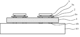
- FIG. 1 is an explanatory diagram of the production method of the present invention.
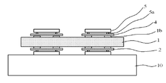
- FIG. 2 is an explanatory diagram of the production method of the present invention.
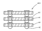
- FIG. 3 is a cross-sectional view of a multilayer electronic component.
- FIG. 4 is an explanatory diagram of the production method of the present invention.
- FIG. 5 is an explanatory diagram of the production method of the present invention.
- FIG. 6 is an explanatory diagram of the production method of the present invention.
- FIG. 7 is a cross-sectional view of the connection structure of the present invention.
- FIG. 8 is a DSC chart showing the curing temperature of the adhesive film.
- the present invention is a method for manufacturing a connection structure including a wiring board, a first electronic component flip-chip mounted on the front surface thereof, and a second electronic component flip-chip mounted on the back surface thereof, and includes the following steps ( A production method having a) to (d).
- a production method having a) to (d) A production method having a) to (d).
- the first electronic component 3 is temporarily installed on the surface of the wiring board 1 via the first adhesive film 2. Specifically, the wiring substrate 1 having the front electrode 1a and the back electrode 1b is placed on the stage 10, the first adhesive film 2 is aligned and temporarily attached on the front electrode 1a, and the bump 3a is placed thereon. The first electronic component 3 having the above is aligned and temporarily installed.
- a platen made of flat metal, ceramics, resin or the like provided with a vacuum chuck mechanism for holding the wiring board 1 in a fixed position can be used.
- a front electrode 1a and a back electrode 1b made of wiring or pads of copper, aluminum, silver, gold, etc. are formed on both surfaces of a substrate such as a glass substrate, a ceramic substrate, a polyimide flexible substrate, or a glass epoxy substrate. The thing which was done is mentioned. These electrodes can be subjected to electrolysis, electroless nickel plating, solder plating, gold plating or the like as required.
- a known ACF or NCF can be used as the first adhesive film 2.
- a liquid or solid epoxy resin as a curing component a phenoxy resin as a film forming component, an acid anhydride or an imidazole as a curing agent for an epoxy resin, and a silane coupling agent as long as the effects of the present invention are not impaired.
- a first adhesive film-forming paint containing a known additive such as a pigment, an antioxidant, a diluent, a solvent, an antistatic agent, etc., which is made into a film using a known method such as a casting method. Can be used.
- Preferred examples of the first electronic component 3 include an IC chip and an optical chip.
- Examples of the bump 3a include a solder bump, a gold bump, and an aluminum bump.
- Au stud bumps are preferable.
- Bumps other than gold bumps can be subjected to electrolysis, electroless nickel plating, solder plating, gold plating or the like as required.
- Step (b)> the second electronic component 5 is temporarily installed on the back surface of the wiring board 1 via the second adhesive film 4 having a curing temperature lower than the curing temperature of the first adhesive film 2.
- the second adhesive film 4 is aligned and temporarily attached onto the back electrode 1 b of the wiring substrate 1, and the second electronic component 5 having the bumps 5 a thereon is aligned and temporarily attached. Install.
- the component configuration of the second adhesive film 4 is basically the same as the component configuration of the first adhesive film 2, but a component having a curing temperature lower than the curing temperature of the first adhesive film 2 needs to be used.
- the curing temperature of the first adhesive film 2 is preferably 200 to 250 ° C.
- the curing temperature of the second adhesive film 4 is preferably 170 to 220 ° C.
- the curing temperature of the 1st adhesive film 2 and the 2nd adhesive film 4 can be determined based on the chart obtained by differential scanning calorimetry (DSC). For example, in the DSC chart, a peak appears when the resin curing reaction proceeds. Therefore, the sample 5 mg was heated from room temperature to 250 ° C. at a rate of 10 ° C./min. The temperature at 60% of the total area was taken as the curing temperature (see FIG. 8).
- DSC differential scanning calorimetry
- the adjustment of the curing temperature of these adhesive films 2 or 4 can be performed by specifying the structure and molecular weight of materials such as epoxy resin, film forming resin, and curing agent to be used.
- the 2nd electronic component 5 and its bump 5a can be set as the structure similar to the 1st electronic component 3 and its bump 3a fundamentally.
- the alignment of the second adhesive film 4 on the back electrode 1b and the temporary attachment thereof the alignment of the second electronic component 5 on the second adhesive film 4 and the provisional installation thereof are also made using a conventionally known method. It can be carried out.
- the second electronic component 5 and the first electronic component 3 described above has a through electrode 41, a front bump 42 connected to the through electrode 41, and a back bump 43, as shown in FIG.
- a plurality of IC chips 40 may be stacked on each other to form the electronic component 400.
- the through electrode 41 can be formed by copper plating
- the front bump 42 and the back bump 43 existing between the IC chips 40 are made of gold, solder, copper, or the like. It is preferable that one or both of them be formed of solder.
- the wiring board 1 on which the first electronic component 3 and the second electronic component 5 are temporarily installed is crimped to a wiring board mounting surface 21 made of an elastic material such as rubber. Place on the table 20.
- a crimping cradle 20 the one disclosed in Japanese Patent Application Laid-Open No. 2007-227622 can be employed. That is, the crimping cradle 20 is composed of a cradle body 22 made of metal or ceramics and an elastic receiving part 23 arranged on the side on which the object to be crimped is placed, and the surface thereof is the wiring board placement surface 21. It is what has become.
- the elastic material preferably means an elastomer having a rubber hardness of 10 to 80.
- stage 10 may be used as the crimping cradle 20 as it is, and although not shown, the one having a recessed portion in which the second electronic component 5 is accommodated and having a relatively rigid wiring board mounting surface. May be used.
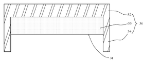
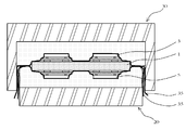
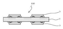
- Step (d)> Finally, the first electronic component 3 is pressed against the wiring board 1 from the first electronic component 3 side with a heating and pressing tool 30 (FIG. 5) having a pressing surface 31 formed of an elastic material such as rubber. By heating while heating, the first electronic component 3 and the second electronic component 5 are collectively mounted on the front surface and the back surface of the wiring substrate 1 as shown in FIG. Thereby, the connection structure 100 shown in FIG. 7 is obtained.
- a heating and pressing tool 30 FIG. 5 having a pressing surface 31 formed of an elastic material such as rubber.
- the heating and pressing tool 30 includes a pressing main body 32 made of metal or ceramics and an elastic pressing portion 33 arranged on the object to be bonded side, and the surface thereof is a pressing surface 31. It is desirable that a side portion 34 is extended to the pressing main body 32 so that the crimping receiving base 20 can be fitted therein.
- the heating means may be provided with a heater (not shown) so as to heat the pressing main body 32, but the pressing main body 32 itself or the elastic pressing portion 33 itself may generate heat.
- the reaching temperature at which the first adhesive film 2 reaches by heating is higher than the reaching temperature at which the second adhesive film 4 reaches by heating.
- the preferable curing temperature of the first adhesive film 2 is 200 to 250 ° C. and the preferable curing temperature of the second adhesive film 4 is 170 to 220 ° C.
- the first adhesive film 2 reaches by heating.
- the ultimate temperature at which the second adhesive film 4 reaches by heating is 170-220 ° C.
- the first electronic component 3 and the second electronic component 5 are temporarily installed when the first electronic component 3 is heated against the wiring board 1 while being pressed from the first electronic component 3 side with the heating and pressing tool 30.
- connection structure shown in FIG. 7 manufactured by the manufacturing method of the present invention described above is optimal for both ACFs and NCFs on both sides of the wiring board when the electronic components are flip-chip mounted via ACFs and NCFs. It is obtained by curing. Therefore, good connection reliability is exhibited without warping of the wiring board.
- Examples 1-2 and Comparative Examples 1-4 NCF showing the curing temperature shown in Table 2 was prepared. Separately, a gold stud bump with a peripheral pitch with a bump pitch of 85 ⁇ m and a bump number of 272 (sometimes abbreviated as “Au stud”) or copper pillar / solder cap bump (sometimes abbreviated as “Cu / solder”). An IC chip for testing (6.3 mm ⁇ 6.3 mm ⁇ 0.2 thickness) was prepared. Also, a glass epoxy double-sided wiring board (FR4, Hitachi Chemical Co., Ltd .: 38 mm ⁇ 38 mm ⁇ 0.6 mm thickness) having electrode pads (Au / Ni plated Cu base) on both sides with a 20 ⁇ m thick solder surface layer formed Prepared.
- FR4 Hitachi Chemical Co., Ltd .: 38 mm ⁇ 38 mm ⁇ 0.6 mm thickness
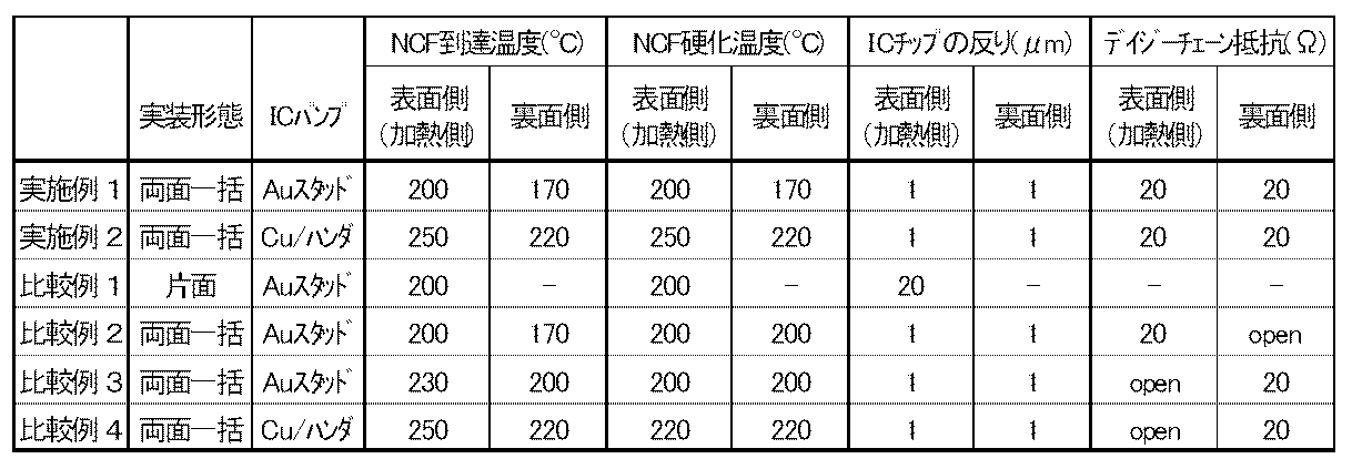
- Table 2 shows the mounting forms of the examples and comparative examples, IC bump types (Au stud bumps, Cu pillar / solder cap bumps), arrival of NCFs arranged on the front side (heating side) and back side of the wiring board. The temperature and the curing temperature of NCF are described.
- the warpage of the IC chip was measured using a stylus type surface roughness meter (SE-3H, Kosaka Laboratory Ltd.). The obtained results are shown in Table 2. Practically, the warp is desirably 10 ⁇ m or less.
- connection structures of Examples 1 and 2 in which NCF having a higher curing temperature is arranged on the surface side (heating side) of the wiring board so as to conform to the NCF ultimate temperature are as follows. Both warpage and daisy chain resistance results were practically favorable. On the other hand, in the case of the single-side mounting of Comparative Example 1, the warpage of the IC chip was significant. In Comparative Examples 2 to 4 using NCF having the same curing temperature on the front side and the back side, the daisy chain resistance was open on the front side or the back side.
- connection structure of the present invention two types of adhesive films having different curing temperatures are used, and the adhesive film having a higher curing temperature is disposed on the surface of the wiring substrate to be heated.
- Adhesive films on both sides can be heated to the optimum curing temperature at a time, improving the connection reliability of double-sided flip chip mounting wiring boards for electronic components without causing warping of wiring boards and IC chips can do. Therefore, the present invention is useful when a connection structure is manufactured by double-side flip chip mounting on a wiring board.
Landscapes
- Chemical & Material Sciences (AREA)
- Organic Chemistry (AREA)
- Engineering & Computer Science (AREA)
- Microelectronics & Electronic Packaging (AREA)
- Wire Bonding (AREA)
- Manufacturing & Machinery (AREA)
Abstract
Description
工程(a)
配線基板の表面に、第1接着フィルムを介して第1電子部品を仮設置する工程;
工程(b)
配線基板の裏面に、第1接着フィルムの硬化温度よりも低い硬化温度を有する第2接着フィルムを介して第2電子部品を仮設置する工程;
工程(c)
第1電子部品及び第2電子部品が仮設置された配線基板を、圧着受け台に載置する工程;及び
工程(d)
第1電子部品を、配線基板に対して第1電子部品側から加熱加圧ツールで押圧しながら加熱することにより、配線基板の表面及び裏面に第1電子部品及び第2電子部品をそれぞれ一括で実装する工程
を有することを特徴とする製造方法、及びこの製造方法により製造された接続構造体を提供する。
まず、図1に示すように、配線基板1の表面に、第1接着フィルム2を介して第1電子部品3を仮設置する。具体的には、ステージ10上に、表面電極1aと裏面電極1bとを有する配線基板1を載せ、表面電極1a上に、第1接着フィルム2をアライメントして仮貼りし、その上にバンプ3aを有する第1電子部品3をアライメントして仮設置する。
次に、図2に示すように、配線基板1の裏面に、第1接着フィルム2の硬化温度よりも低い硬化温度を有する第2接着フィルム4を介して第2電子部品5を仮設置する。具体的には、ステージ10上において、配線基板1の裏面電極1b上に、第2接着フィルム4をアライメントして仮貼りし、その上にバンプ5aを有する第2電子部品5をアライメントして仮設置する。
次に、図4に示すように、第1電子部品3及び第2電子部品5が仮設置された配線基板1を、ゴムなどの弾性材料から形成された配線基板載置面21を有する圧着受け台20に載置する。このような圧着受け台20としては、特開2007-227622号公報に開示されているものを採用することができる。即ち、圧着受け台20は、金属やセラミックスからなる受け台本体22と、被圧着物が載置される側に配置される弾性受け部23とから構成され、その表面が配線基板載置面21となっているものである。ここで、本発明において、弾性材料とは、好ましくはゴム硬度が10~80のエラストマーを意味する。
最後に、第1電子部品3を、配線基板1に対して第1電子部品3側から、ゴムなどの弾性材料から形成されている押圧面31を有する加熱加圧ツール30(図5)で押圧しながら加熱することにより、図6に示すように配線基板1の表面及び裏面に第1電子部品3及び第2電子部品5をそれぞれ一括で実装する。これにより図7に示す接続構造体100が得られる。
表2に示した硬化温度を示すNCFを用意した。それとは別に、バンプピッチ85μm、バンプ数272のペリフェラル配置の金スタッドバンプ(“Auスタッド”と略する場合がある)又は銅ピラー/ハンダキャップバンプ(“Cu/ハンダ”と略する場合がある)が設けられた試験用ICチップ(6.3mm×6.3mm×0.2厚)を用意した。また、20μm厚のハンダ表面層が形成された電極パッド(Au/NiメッキCuベース)を両面に有するガラスエポキシ両面配線基板(FR4、日立化成工業(株):38mm×38mm×0.6mm厚)を用意した。

1a 表面電極
1b 裏面電極
2 第1接着フィルム
3 第1電子部品
3a バンプ
4 第2接着フィルム
5 第2電子部品
5a バンプ
10 ステージ
20 圧着受け台
21 配線基板載置面
22 受け台本体
23 弾性受け部
30 加熱加圧ツール
31 押圧面
32 押圧本体
33 弾性押圧部
34 側部
35 保護シート
100 接続構造体
40 ICチップ
41 貫通電極
42 フロントバンプ
43 バックバンプ
400 積層型の電子部品
Claims (9)
- 配線基板と、その表面にフリップチップ実装された第1電子部品と、裏面にフリップチップ実装された第2電子部品とを含む接続構造体の製造方法であって、以下の工程(a)~(d):
工程(a)
配線基板の表面に、第1接着フィルムを介して第1電子部品を仮設置する工程;
工程(b)
配線基板の裏面に、第1接着フィルムの硬化温度よりも低い硬化温度を有する第2接着フィルムを介して第2電子部品を仮設置する工程;
工程(c)
第1電子部品及び第2電子部品が仮設置された配線基板を、圧着受け台に載置する工程;及び
工程(d)
第1電子部品を、配線基板に対して第1電子部品側から加熱加圧ツールで押圧しながら加熱することにより、配線基板の表面及び裏面に第1電子部品及び第2電子部品をそれぞれ一括で実装する工程
を有することを特徴とする製造方法。 - 工程(d)において、加熱加圧ツールによる加熱押圧の際に、第1接着フィルムが加熱により到達した到達温度が、第2接着フィルムが加熱により到達した到達温度よりも高い請求項1記載の製造方法。
- 第1接着フィルムの硬化温度が200~250℃であり、第2接着フィルムの硬化温度が170~220℃である請求項1又は2記載の製造方法。
- 加熱加圧ツールの押圧面が弾性材料から形成されている請求項1~3のいずれかに記載の製造方法。
- 第1電子部品及び第2電子部品が仮設置された配線基板が、第2電子部品側から載置される圧着受け台の配線基板載置面が、弾性材料から形成されている請求項4記載の製造方法。
- 工程(d)において、第1電子部品を、配線基板に対して第1電子部品側から加熱加圧ツールで押圧しながら加熱する際に、第1電子部品及び第2電子部品が仮設置された配線基板の両面に保護シートを配置させて押圧する請求項1~5のいずれかに記載の製造方法。
- 第1電子部品及び第2電子部品の少なくともいずれか一方がICチップである請求項1~6のいずれかに記載の製造方法。
- 第1電子部品及び第2電子部品の少なくともいずれか一方が、貫通電極とそれに接続しているフロントバンプとバックバンプとを有し、互いに積層されるべき複数のICチップであり、ICチップ間に存在するフロントバンプ及びバックバンプの少なくともいずれか一方がハンダで形成されている請求項1又は2記載の製造方法。
- 請求項1~8の製造方法により製造された接続構造体。
Priority Applications (2)
| Application Number | Priority Date | Filing Date | Title |
|---|---|---|---|
| KR1020137027942A KR101858783B1 (ko) | 2011-04-27 | 2012-04-02 | 접속 구조체의 제조 방법 |
| US14/112,277 US9318353B2 (en) | 2011-04-27 | 2012-04-02 | Method of manufacturing connection structure |
Applications Claiming Priority (2)
| Application Number | Priority Date | Filing Date | Title |
|---|---|---|---|
| JP2011-098967 | 2011-04-27 | ||
| JP2011098967A JP5741188B2 (ja) | 2011-04-27 | 2011-04-27 | 接続構造体の製造方法 |
Publications (1)
| Publication Number | Publication Date |
|---|---|
| WO2012147458A1 true WO2012147458A1 (ja) | 2012-11-01 |
Family
ID=47071983
Family Applications (1)
| Application Number | Title | Priority Date | Filing Date |
|---|---|---|---|
| PCT/JP2012/058889 Ceased WO2012147458A1 (ja) | 2011-04-27 | 2012-04-02 | 接続構造体の製造方法 |
Country Status (5)
| Country | Link |
|---|---|
| US (1) | US9318353B2 (ja) |
| JP (1) | JP5741188B2 (ja) |
| KR (1) | KR101858783B1 (ja) |
| TW (1) | TWI494038B (ja) |
| WO (1) | WO2012147458A1 (ja) |
Families Citing this family (4)
| Publication number | Priority date | Publication date | Assignee | Title |
|---|---|---|---|---|
| CN105493207B (zh) * | 2014-02-24 | 2018-05-25 | 积水化学工业株式会社 | 连接结构体的制造方法 |
| JP2016162985A (ja) | 2015-03-05 | 2016-09-05 | ルネサスエレクトロニクス株式会社 | 半導体装置の製造方法 |
| JP6271463B2 (ja) * | 2015-03-11 | 2018-01-31 | 東芝メモリ株式会社 | 半導体装置 |
| KR102322766B1 (ko) | 2015-09-03 | 2021-11-08 | 삼성디스플레이 주식회사 | 디스플레이 장치 |
Citations (3)
| Publication number | Priority date | Publication date | Assignee | Title |
|---|---|---|---|---|
| JP2000003922A (ja) * | 1998-06-16 | 2000-01-07 | Nitto Denko Corp | 半導体装置の製法 |
| JP2001326322A (ja) * | 2000-05-17 | 2001-11-22 | Matsushita Electric Ind Co Ltd | 半導体実装対象中間構造体及び半導体装置の製造方法 |
| JP2006229106A (ja) * | 2005-02-21 | 2006-08-31 | Matsushita Electric Ind Co Ltd | 半導体装置の実装方法と実装装置および半導体装置 |
Family Cites Families (8)
| Publication number | Priority date | Publication date | Assignee | Title |
|---|---|---|---|---|
| JPS5376372A (en) * | 1976-12-17 | 1978-07-06 | Matsushita Electric Industrial Co Ltd | Device for attaching chip circuit parts |
| DE3104623A1 (de) * | 1981-02-10 | 1982-08-26 | Robert Bosch Gmbh, 7000 Stuttgart | Verfahren zum befestigen von bauelementen mit flaechigen anschlusskontakten und bauelement hierfuer |
| US4761881A (en) * | 1986-09-15 | 1988-08-09 | International Business Machines Corporation | Single step solder process |
| US5155904A (en) * | 1991-04-03 | 1992-10-20 | Compaq Computer Corporation | Reflow and wave soldering techniques for bottom side components |
| US5678304A (en) * | 1996-07-24 | 1997-10-21 | Eastman Kodak Company | Method for manufacturing double-sided circuit assemblies |
| JP2001332682A (ja) * | 2000-05-19 | 2001-11-30 | Matsushita Electric Ind Co Ltd | 半導体素子実装方法および半導体素子実装構造 |
| JP4441328B2 (ja) * | 2004-05-25 | 2010-03-31 | 株式会社ルネサステクノロジ | 半導体装置及びその製造方法 |
| JP4832107B2 (ja) | 2006-02-23 | 2011-12-07 | ソニーケミカル&インフォメーションデバイス株式会社 | 実装方法 |
-
2011
- 2011-04-27 JP JP2011098967A patent/JP5741188B2/ja active Active
-
2012
- 2012-04-02 US US14/112,277 patent/US9318353B2/en active Active
- 2012-04-02 WO PCT/JP2012/058889 patent/WO2012147458A1/ja not_active Ceased
- 2012-04-02 KR KR1020137027942A patent/KR101858783B1/ko active Active
- 2012-04-16 TW TW101113431A patent/TWI494038B/zh active
Patent Citations (3)
| Publication number | Priority date | Publication date | Assignee | Title |
|---|---|---|---|---|
| JP2000003922A (ja) * | 1998-06-16 | 2000-01-07 | Nitto Denko Corp | 半導体装置の製法 |
| JP2001326322A (ja) * | 2000-05-17 | 2001-11-22 | Matsushita Electric Ind Co Ltd | 半導体実装対象中間構造体及び半導体装置の製造方法 |
| JP2006229106A (ja) * | 2005-02-21 | 2006-08-31 | Matsushita Electric Ind Co Ltd | 半導体装置の実装方法と実装装置および半導体装置 |
Also Published As
| Publication number | Publication date |
|---|---|
| TW201251553A (en) | 2012-12-16 |
| KR101858783B1 (ko) | 2018-05-16 |
| US20140226297A1 (en) | 2014-08-14 |
| US9318353B2 (en) | 2016-04-19 |
| JP2012231039A (ja) | 2012-11-22 |
| JP5741188B2 (ja) | 2015-07-01 |
| KR20140031872A (ko) | 2014-03-13 |
| TWI494038B (zh) | 2015-07-21 |
Similar Documents
| Publication | Publication Date | Title |
|---|---|---|
| JP6718106B2 (ja) | 実装構造体の製造方法 | |
| CN101322233B (zh) | 使用超声振动在电气器件之间结合的方法 | |
| CN1194059A (zh) | 用于粘合电子器件的可变形基片部件 | |
| JP5191627B2 (ja) | フィルム状接着剤およびこれを用いた半導体装置の製造方法 | |
| CN102977809A (zh) | 电路部件连接用粘接剂以及半导体装置 | |
| JP5741188B2 (ja) | 接続構造体の製造方法 | |
| CN107112659A (zh) | 连接结构体的制造方法 | |
| JP5906022B2 (ja) | マクロピンハイブリッド相互接続アレイ及びその製造方法 | |
| JP2009157186A (ja) | 平面表示装置、及びこの製造方法 | |
| KR101763852B1 (ko) | Qfn 반도체 패키지, 이의 제조방법 및 qfn 반도체 패키지 제조용 마스크 시트 | |
| CN1943029A (zh) | 半导体器件及其制造方法 | |
| CN101529662A (zh) | 连接电路板的方法以及连接结构 | |
| CN100596262C (zh) | 用于相互连接电路板的方法 | |
| JP6007022B2 (ja) | 回路接続材料 | |
| JP5433923B2 (ja) | スティフナ付き基板およびその製造方法 | |
| JP5912611B2 (ja) | フィルム状接着剤 | |
| JPWO2009072497A1 (ja) | 回路部材接続用接着剤及び半導体装置 | |
| JP4254849B2 (ja) | マルチチップ実装法 | |
| JP2003347366A (ja) | 半導体装置用テープキャリア、半導体装置およびその半導体装置の製造方法 | |
| JP2008219052A (ja) | 半導体装置の製造方法 | |
| KR102032767B1 (ko) | Qfn 반도체 패키지, 이의 제조방법 및 qfn 반도체 패키지 제조용 마스크 시트 | |
| JP4080681B2 (ja) | 電子部品実装用フィルムキャリアテープおよびその製造方法 | |
| TWI361301B (en) | Display device including flip chip structure | |
| Zhang et al. | The effect of the different teflon films on anisotropic conductive adhesive film (ACF) bonding | |
| JP2003332510A (ja) | 放熱板付きリードフレーム固定用接着基材 |
Legal Events
| Date | Code | Title | Description |
|---|---|---|---|
| 121 | Ep: the epo has been informed by wipo that ep was designated in this application |
Ref document number: 12777766 Country of ref document: EP Kind code of ref document: A1 |
|
| WWE | Wipo information: entry into national phase |
Ref document number: 14112277 Country of ref document: US |
|
| ENP | Entry into the national phase |
Ref document number: 20137027942 Country of ref document: KR Kind code of ref document: A |
|
| NENP | Non-entry into the national phase |
Ref country code: DE |
|
| 122 | Ep: pct application non-entry in european phase |
Ref document number: 12777766 Country of ref document: EP Kind code of ref document: A1 |