WO2012132970A1 - プリント配線基板およびその製造方法、並びに、金属表面処理液 - Google Patents
プリント配線基板およびその製造方法、並びに、金属表面処理液 Download PDFInfo
- Publication number
- WO2012132970A1 WO2012132970A1 PCT/JP2012/056904 JP2012056904W WO2012132970A1 WO 2012132970 A1 WO2012132970 A1 WO 2012132970A1 JP 2012056904 W JP2012056904 W JP 2012056904W WO 2012132970 A1 WO2012132970 A1 WO 2012132970A1
- Authority
- WO
- WIPO (PCT)
- Prior art keywords
- thiol compound
- insulating layer
- wiring board
- substrate
- metal wiring
- Prior art date
- Legal status (The legal status is an assumption and is not a legal conclusion. Google has not performed a legal analysis and makes no representation as to the accuracy of the status listed.)
- Ceased
Links
Images


Classifications
-
- H—ELECTRICITY
- H05—ELECTRIC TECHNIQUES NOT OTHERWISE PROVIDED FOR
- H05K—PRINTED CIRCUITS; CASINGS OR CONSTRUCTIONAL DETAILS OF ELECTRIC APPARATUS; MANUFACTURE OF ASSEMBLAGES OF ELECTRICAL COMPONENTS
- H05K1/00—Printed circuits
- H05K1/02—Details
- H05K1/0213—Electrical arrangements not otherwise provided for
- H05K1/0237—High frequency adaptations
-
- H—ELECTRICITY
- H05—ELECTRIC TECHNIQUES NOT OTHERWISE PROVIDED FOR
- H05K—PRINTED CIRCUITS; CASINGS OR CONSTRUCTIONAL DETAILS OF ELECTRIC APPARATUS; MANUFACTURE OF ASSEMBLAGES OF ELECTRICAL COMPONENTS
- H05K3/00—Apparatus or processes for manufacturing printed circuits
- H05K3/38—Improvement of the adhesion between the insulating substrate and the metal
-
- H—ELECTRICITY
- H05—ELECTRIC TECHNIQUES NOT OTHERWISE PROVIDED FOR
- H05K—PRINTED CIRCUITS; CASINGS OR CONSTRUCTIONAL DETAILS OF ELECTRIC APPARATUS; MANUFACTURE OF ASSEMBLAGES OF ELECTRICAL COMPONENTS
- H05K3/00—Apparatus or processes for manufacturing printed circuits
- H05K3/38—Improvement of the adhesion between the insulating substrate and the metal
- H05K3/389—Improvement of the adhesion between the insulating substrate and the metal by the use of a coupling agent, e.g. silane
-
- H—ELECTRICITY
- H05—ELECTRIC TECHNIQUES NOT OTHERWISE PROVIDED FOR
- H05K—PRINTED CIRCUITS; CASINGS OR CONSTRUCTIONAL DETAILS OF ELECTRIC APPARATUS; MANUFACTURE OF ASSEMBLAGES OF ELECTRICAL COMPONENTS
- H05K3/00—Apparatus or processes for manufacturing printed circuits
- H05K3/44—Manufacturing insulated metal core circuits or other insulated electrically conductive core circuits
-
- H—ELECTRICITY
- H05—ELECTRIC TECHNIQUES NOT OTHERWISE PROVIDED FOR
- H05K—PRINTED CIRCUITS; CASINGS OR CONSTRUCTIONAL DETAILS OF ELECTRIC APPARATUS; MANUFACTURE OF ASSEMBLAGES OF ELECTRICAL COMPONENTS
- H05K3/00—Apparatus or processes for manufacturing printed circuits
- H05K3/46—Manufacturing multilayer circuits
- H05K3/4644—Manufacturing multilayer circuits by building the multilayer layer by layer, i.e. build-up multilayer circuits
- H05K3/4673—Application methods or materials of intermediate insulating layers not specially adapted to any one of the previous methods of adding a circuit layer
-
- H—ELECTRICITY
- H05—ELECTRIC TECHNIQUES NOT OTHERWISE PROVIDED FOR
- H05K—PRINTED CIRCUITS; CASINGS OR CONSTRUCTIONAL DETAILS OF ELECTRIC APPARATUS; MANUFACTURE OF ASSEMBLAGES OF ELECTRICAL COMPONENTS
- H05K2203/00—Indexing scheme relating to apparatus or processes for manufacturing printed circuits covered by H05K3/00
- H05K2203/12—Using specific substances
- H05K2203/122—Organic non-polymeric compounds, e.g. oil, wax or thiol
Definitions
- the present invention relates to a printed wiring board, a manufacturing method thereof, and a metal surface treatment liquid.
- a printed wiring board is obtained by laminating one or more metal wirings and insulating layers. At that time, if the adhesion between the metal wiring and the insulating layer is insufficient, a gap is formed between the metal wiring and the insulating layer, and if water vapor enters the metal wiring, the electrical insulation deteriorates or the wiring is short-circuited.
- a technique for improving the adhesion between the metal wiring and the insulating layer a technique for roughening the surface of the metal wiring and generating an anchor effect has been used.
- the width of the metal wiring is narrowing, there is a problem that it is difficult to roughen the surface of the metal wiring and the high frequency characteristics are deteriorated due to the formed unevenness. .
- Patent Document 1 a method of treating the metal wiring surface with a triazine thiol derivative has been proposed.
- An object of this invention is to provide the printed wiring board excellent in the adhesiveness of an insulating layer, and its manufacturing method in view of the said situation.
- Another object of the present invention is to provide a metal surface treatment solution for a printed wiring board for surface treatment of the metal wiring used in the production method.
- a printed wiring board comprising an insulating substrate, a metal wiring disposed on the insulating substrate, and an insulating layer disposed on the metal wiring, A printed wiring board in which a layer of a thiol compound having four or more functional groups represented by formula (1) described later is interposed at an interface between a metal wiring and an insulating layer.
- a thiol equivalent (g / eq) of the thiol compound is 2100 or less.
- the printed wiring board excellent in the adhesiveness of the insulating layer and its manufacturing method can be provided.
- the metal surface treatment liquid for printed wiring boards for surface-treating the metal wiring used by this manufacturing method can also be provided.
- a feature of the present invention is that a layer of a thiol compound (hereinafter also simply referred to as a thiol compound) containing four or more functional groups (hereinafter also referred to as a functional group A) represented by the formula (1) described later is a metal
- a thiol compound hereinafter also simply referred to as a thiol compound
- four or more functional groups hereinafter also referred to as a functional group A
- the compound layer plays a role of assisting adhesion between the metal wiring and the insulating layer (role of the adhesion assisting layer).
- the compound binds to the metal wiring via the functional group A and increases the affinity for the insulating layer.
- the insulating layer contains an epoxy resin having an epoxy group or a (meth) acrylate resin having a (meth) acrylate group, it is excellent in reactivity with the compound, and as a result, between the metal wiring and the insulating layer. Adhesion is better.
- the method for manufacturing a printed wiring board according to the present invention preferably includes a wiring processing step, a drying step, and an insulating layer forming step.
- a drying process is arbitrary processes and is implemented as needed.
- a core substrate (insulating substrate with metal wiring) having an insulating substrate and metal wiring disposed on the insulating substrate, and four or more functional groups represented by the following formula (1) are included.
- a metal surface treatment liquid containing a thiol compound is brought into contact (contact process).
- the obtained core substrate is cleaned with a solvent (cleaning solvent) (cleaning step).
- the contact step is a step in which the core substrate and the metal surface treatment liquid are brought into contact and the insulating substrate surface and the metal wiring surface of the core substrate are covered with a thiol compound.
- the cleaning process is a process of removing the thiol compound on the surface of the insulating substrate by cleaning the core substrate using a solvent.
- the thiol compound is bonded so as to cover the surface of the metal wiring, and the adhesion between the insulating layer and the core substrate described later is improved.
- materials core substrate, metal surface treatment liquid, cleaning solvent, etc. used in the wiring processing step will be described, and then the procedure of the step will be described.
- the core substrate (inner layer substrate) used in this step has an insulating substrate and metal wiring disposed on the insulating substrate, and the metal wiring may be disposed in the outermost layer.
- the core substrate has a laminated structure having at least an insulating substrate and metal wiring, and the metal wiring is arranged in the outermost layer.
- FIG. 1A shows an embodiment of a core substrate.
- the core substrate 10 includes an insulating substrate 12 and metal wirings 14 disposed on the insulating substrate 12.
- the metal wiring 14 is provided only on one side of the substrate, but may be provided on both sides. That is, the core substrate 10 may be a single-sided substrate or a double-sided substrate.
- the insulating substrate is not particularly limited as long as it can support metal wiring.
- an organic substrate, a ceramic substrate, a silicon substrate, a glass substrate, or the like can be used.
- Resin is mentioned as a material of an organic substrate,
- a thermosetting resin, a thermoplastic resin, or resin which mixed them examples include phenol resin, urea resin, melamine resin, alkyd resin, acrylic resin, unsaturated polyester resin, diallyl phthalate resin, epoxy resin, silicone resin, furan resin, ketone resin, xylene resin, benzocyclo Examples include butene resin.
- thermoplastic resin examples include polyimide resin, polyphenylene oxide resin, polyphenylene sulfide resin, aramid resin, and liquid crystal polymer.
- a glass woven fabric, a glass nonwoven fabric, an aramid woven fabric, an aramid nonwoven fabric, an aromatic polyamide woven fabric, a material impregnated with the above resin, or the like can be used as a material of the organic substrate.
- the metal wiring is mainly composed of metal.
- the type of metal is not particularly limited, and examples thereof include copper or copper alloy, silver or silver alloy, tin, palladium, gold, nickel, chromium, platinum, iron, gallium, indium, and combinations thereof.
- the method for forming the metal wiring on the insulating substrate is not particularly limited, and a known method can be adopted. Typically, a subtractive method using an etching process and a semi-additive method using electrolytic plating can be given.
- the metal wiring may contain an organic substance such as a binder resin as long as the effects of the present invention are not impaired.
- the width of the metal wiring is not particularly limited, but is preferably 0.5 to 1000 ⁇ m, more preferably 0.5 to 25 ⁇ m, and still more preferably 0.5 to 10 ⁇ m from the viewpoint of high integration of the printed wiring board.
- the interval between the metal wirings is not particularly limited, but is preferably 0.5 to 1000 ⁇ m, more preferably 0.5 to 25 ⁇ m, and further preferably 0.5 to 10 ⁇ m from the viewpoint of high integration of the printed wiring board.
- the pattern shape of the metal wiring is not particularly limited, and may be an arbitrary pattern. For example, a linear shape, a curved shape, a rectangular shape, a circular shape, and the like can be given.
- the thickness of the metal wiring is not particularly limited, but is preferably 1 to 1000 ⁇ m, more preferably 3 to 25 ⁇ m, and further preferably 10 to 20 ⁇ m from the viewpoint of high integration of the printed wiring board.
- the surface roughness Rz of the metal wiring is not particularly limited, but is preferably 10 ⁇ m or less, more preferably 0.001 to 2 ⁇ m, and more preferably 0.01 to 0.9 ⁇ m from the viewpoint of the high frequency characteristics of the printed wiring board to be obtained. Further preferred is 0.02 to 0.5 ⁇ m. Rz is measured according to JIS B 0601 (1994).
- Another aspect of the core substrate used in this step is a multilayer wiring substrate having two or more insulating substrates and two or more metal wirings alternately.
- another metal wiring 50 (metal wiring layer) and another insulating substrate 40 may be provided in this order between the insulating substrate 12 and the metal wiring 14 (see FIG. 2).
- the other metal wiring 50 and the other insulating substrate 40 may be alternately included in two layers or more in this order between the substrate 12 and the metal wiring 14.
- the core substrate 10 may be a so-called rigid substrate, flexible substrate, or rigid flexible substrate.
- a through hole may be formed in the insulating substrate.
- the metal wiring on both surfaces may be made conductive by filling the through hole with metal (for example, copper or copper alloy).
- the metal surface treatment liquid used in this step contains a thiol compound having four or more functional groups represented by formula (1) (hereinafter also referred to as functional group A as appropriate).
- functional group A represents a bonding position.
- the processing liquid is used for improving the adhesion between the metal wiring in the printed wiring board and an insulating layer described later, and is a processing liquid for processing the surface of the metal wiring. That is, it is a treatment liquid that improves the adhesion between the metal wiring and the insulating layer by applying a thiol compound to the metal wiring.
- a thiol compound is described in detail below, and then optional components (such as a solvent) are described in detail.
- the thiol compound contains four or more functional groups A. By including four or more groups, adhesion between the metal wiring in the core substrate and the insulating layer is improved.
- the upper limit of the number of functional groups A is not particularly limited, but is preferably 200 or less from the viewpoint of compound synthesis.
- the number of functional groups A is preferably 4 to 20, more preferably 4 to 10, and even more preferably 4 to 6 from the viewpoint of better adhesion of the insulating layer. When the number of functional groups A is 3 or less, the adhesion of the insulating layer is extremely inferior.
- a desired effect is acquired by having the functional group (what is called primary thiol group) represented by Formula (1) which HS group couple
- a so-called secondary thiol group such as —C (CH 3 ) H—SH
- a disulfide group such as —S—SH
- the activity of the HS group is increased. Low. Therefore, when a compound having these groups is used, the adhesion of the insulating layer is extremely inferior.
- the thiol equivalent (g / eq) of the thiol compound is not particularly limited, but is preferably 2100 or less, more preferably 400 or less, and even more preferably 250 or less, in terms of better adhesion of the insulating layer.
- limit in particular regarding a minimum from the point on the synthesis
- the thiol equivalent represents the molecular size per unit quantity of mercapto groups (HS groups) contained in the thiol compound.
- the molecular weight of the thiol compound is not particularly limited, it is preferably 8400 or less, more preferably 3000 or less, and particularly preferably 2000 or less, in terms of better adhesion of the insulating layer and superior solubility in a solvent.
- limit in particular regarding a minimum Usually, it is 200 or more from the point on the synthesis
- the sulfur atom content (sulfur atom content ratio) in the thiol compound is not particularly limited, but is preferably 20 wt% or more and more preferably 24 to 70 wt% in terms of better adhesion of the insulating layer. Of these, 35 wt% or more is preferable, and 35 to 64 wt% is more preferable in terms of particularly excellent adhesion of the insulating layer. In addition, this sulfur atom content represents content (mass%) of the sulfur atom in the total molecular weight of a thiol compound.
- the thiol compound may contain silicon atoms, but the mass ratio between the silicon atom content and the HS group content (silicon atom content / HS group content) is 0.7 or less. Preferably, it is 0.44 or less, more preferably 0.22 or less. The lower limit is not particularly limited and is 0. If it is the said range, the adhesiveness of an insulating layer will be more excellent.
- HS group content represents content (mass%) of HS group in the total molecular weight of a thiol compound
- silicon atom content is content (mass of silicon atom in the total molecular weight of a thiol compound). %).
- the mass ratio between the silicon atom content and the sulfur atom content is preferably 0.35 or less, It is more preferably 0.18 or less, and further preferably 0.09 or less.
- the lower limit is not particularly limited and is 0. If it is the said range, the adhesiveness of an insulating layer will be more excellent.
- a preferred embodiment of the thiol compound is a thiol compound represented by the following formula (2). If it is this aspect, it is excellent by the adhesiveness of an insulating layer.
- L 1 represents a single bond or a divalent linking group.
- the divalent linking group include a divalent aliphatic hydrocarbon group (preferably having 1 to 8 carbon atoms), a divalent aromatic hydrocarbon group (preferably having 6 to 12 carbon atoms), —O—, —S. —, —SO 2 —, —N (R) — (R: alkyl group), —CO—, —NH—, —COO—, —CONH—, or a combination thereof (eg, alkyleneoxy group, alkylene Oxycarbonyl group, alkylenecarbonyloxy group, etc.).
- divalent aliphatic hydrocarbon group examples include a methylene group, an ethylene group, a propylene group, or a butylene group.
- divalent aromatic hydrocarbon group examples include a phenylene group and a naphthylene group.
- X represents an n-valent hydrocarbon group which may contain a sulfur atom or an oxygen atom.
- the number of carbon atoms of the hydrocarbon group is not particularly limited, but is preferably 1 to 20 carbon atoms and more preferably 1 to 8 carbon atoms from the viewpoints of handleability and solubility in a solvent.
- examples of the hydrocarbon group include an aliphatic hydrocarbon group, an aromatic hydrocarbon group, and a group obtained by combining these.
- the aliphatic hydrocarbon group is not particularly limited, and preferably has 1 to 10 carbon atoms, more preferably 1 to 8 carbon atoms, from the viewpoints of easy handling and better adhesion of the insulating layer.
- the aromatic hydrocarbon group is not particularly limited, and preferably has 1 to 10 carbon atoms and more preferably 1 to 7 carbon atoms from the viewpoints of excellent handleability and better adhesion of the insulating layer.
- n represents an integer of 4 or more. Among these, 4 to 20 is preferable and 4 to 6 is more preferable in terms of easy synthesis and better adhesion of the insulating layer.
- a preferred embodiment of the thiol compound represented by the formula (2) includes a thiol compound represented by the formula (3). If it is this aspect, the adhesiveness of an insulating layer is more excellent.
- L 2 represents a divalent aliphatic hydrocarbon group which may contain —COO—, —S—, or —O—.
- the preferred range of the carbon number of the aliphatic hydrocarbon group is the same as the preferred range of the aliphatic hydrocarbon group of L 1 described above.
- an aliphatic hydrocarbon group containing —COO—, —S—, or —O— is preferable, and an aliphatic hydrocarbon group containing —S— is preferable in that the effect of the present invention is more excellent. Is more preferable.
- Y represents an n-valent aliphatic hydrocarbon group which may contain a sulfur atom or an oxygen atom.
- the preferred range of the number of carbon atoms of the aliphatic hydrocarbon group is the same as the preferred range of the aliphatic hydrocarbon group for X.
- equation (4) or Formula (5) is mentioned.
- L 3 represents an oxygen atom or a divalent aliphatic hydrocarbon group containing an oxygen atom (preferably having 1 to 20 carbon atoms, more preferably 1 to 10). Represents the total number of carbon atoms contained therein.)
- * represents the bonding position with the L 2 group.
- a thiol compound may be used individually by 1 type, and may use 2 or more types simultaneously.
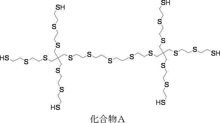
- thiol compound examples include, for example, Pentaerythritol tetrakis (3-mercaptopropionate), Dipentaerythritol hexakis (3-mercaptopropionate), tetrakis- (7-mercapto-2,5-dithiaheptyl) methane, and the following compound A. Tetrakis- (7-mercapto-2,5-dithiaheptyl) methane and compound A are particularly preferred from the viewpoint of better adhesion of the insulating layer.
- the content of the thiol compound in the metal surface treatment solution is not particularly limited, but is preferably 0.01 to 10 mM (mmol), more preferably 0.05 to 3 mM, in terms of better adhesion of the insulating layer. 1 to 1 mM is more preferable.
- the content of the thiol compound is too large, it becomes difficult to control the amount of the thiol compound bonded to the metal wiring, and it is uneconomical. If the content of the thiol compound is too small, it takes time to bond the thiol compound and the productivity is poor.
- the treatment liquid may contain a solvent (particularly a solvent in which the thiol compound is dissolved).
- the solvent used is not particularly limited.
- water alcohol solvents (for example, methanol, ethanol, isopropanol), ketone solvents (for example, acetone, methyl ethyl ketone, cyclohexanone), amide solvents (for example, formamide, dimethylacetamide) N-methylpyrrolidone, N-ethylpyrrolidone), nitrile solvents (eg acetonitrile, propionitrile), ester solvents (eg methyl acetate, ethyl acetate, ⁇ -butyrolactone), carbonate solvents (eg dimethyl carbonate) , Diethyl carbonate), ether solvents (eg cellosolve, tetrahydrofuran), halogen solvents, glycol ether solvents (eg dipropylene glycol methyl ether), glycol ester solvent
- the metal wiring may be dissolved, and the use thereof is not preferable.
- the copper wiring is partially dissolved, and further, the thiol compound and the metal complex are A copper coating may be formed in layers.
- the adhesion of the insulating layer may be reduced, which is not preferable.
- the content of the solvent in the treatment liquid is not particularly limited, but is preferably 90 to 99.99% by mass, more preferably 95 to 99.99% by mass, and 97 to 99.99% by mass with respect to the total amount of the treatment liquid. Particularly preferred.
- the treatment liquid does not substantially contain a resin having a functional group that reacts with a thiol compound (hereinafter also referred to as resin X.
- resin X a resin having a functional group that reacts with a thiol compound
- resin X an epoxy resin, an acrylic resin having an acrylate group, or the like.
- the reaction proceeds with the thiol compound, and the stability of the treatment liquid itself is impaired. Furthermore, it becomes difficult to bond a desired amount of thiol compound on the metal wiring, and as a result, the adhesion of the insulating layer is lowered.
- the resin X is not substantially contained means that the content of the resin X in the processing liquid is 1% by mass or less with respect to the total amount of the processing liquid. In particular, it is preferable that the resin X is not contained (0% by mass).
- the treatment liquid may contain additives such as a pH adjuster, a surfactant, a preservative, and a precipitation inhibitor.
- the solvent (cleaning solvent) used in the cleaning process for cleaning the core substrate is not particularly limited as long as it can remove excess thiol compound and the like deposited between the metal wirings on the insulating substrate. Especially, it is preferable that it is a solvent in which a thiol compound dissolves. By using the solvent, it is possible to more efficiently remove excess thiol compounds deposited on the insulating substrate, excess thiol compounds on the metal wiring, and the like.
- the solvent examples include water, alcohol solvents (eg, methanol, ethanol, propanol), ketone solvents (eg, acetone, methyl ethyl ketone, cyclohexanone), amide solvents (eg, formamide, dimethylacetamide, N-methylpyrrolidone, N-ethylpyrrolidone), nitrile solvents (eg acetonitrile, propionitrile), ester solvents (eg methyl acetate, ethyl acetate, ⁇ -butyrolactone), carbonate solvents (eg dimethyl carbonate, diethyl carbonate), ethers Solvent (eg cellosolve, tetrahydrofuran), halogen solvent, glycol ether solvent (eg dipropylene glycol methyl ether), glycol ester solvent (eg propylene glycol) Monoethyl ether acetate, diethylene glycol monoethyl ether acetate) and the
- solvents Two or more of these solvents may be mixed and used.
- alcohol solvents ketone solvents (preferably cyclohexanone), glycol ester solvents (preferably propylene glycol monomethyl ether acetate, diethylene glycol monoethyl ether acetate), amide solvents (preferably from the viewpoint of the removal of thiol compounds.
- glycol ester solvents preferably propylene glycol monomethyl ether acetate, diethylene glycol monoethyl ether acetate
- amide solvents preferably from the viewpoint of the removal of thiol compounds.
- Is preferably N-ethylpyrrolidone
- a mixed solvent of these solvents and water preferably N-ethylpyrrolidone
- the boiling point (25 ° C., 1 atm) of the solvent used is not particularly limited, but is preferably 75 to 200 ° C., more preferably 80 to 180 ° C. from the viewpoint of safety.
- the thiol compound layer 16 is formed on the core substrate 10 as shown in FIG. It is formed.
- the layer 16 is formed on the insulating substrate 12 and the metal wiring 14.
- the contact step is a step of covering the surface of the insulating substrate 12 and the surface of the metal wiring 14 of the core substrate 10 with a thiol compound layer using the metal surface treatment liquid.
- the thiol compound on the surface of the metal wiring 14 is bonded to the surface of the metal wiring 14 through a thiol group.
- the contact method between the core substrate and the metal surface treatment liquid is not particularly limited, and a known method such as applying a metal surface treatment liquid onto the core substrate can be employed.
- a known method such as applying a metal surface treatment liquid onto the core substrate can be employed.
- dip dipping, shower spraying, spray coating, spin coating and the like can be mentioned, and dip dipping, shower spraying and spray coating are preferred from the standpoint of easy processing and easy adjustment of processing time.
- the temperature of the treatment liquid at the time of contact is preferably in the range of 5 to 75 ° C., more preferably in the range of 10 to 45 ° C., and more preferably in the range of 15 to 35 in terms of controlling the adhesion amount (bonding amount) of the thiol compound.
- a range of ° C is more preferred.
- the contact time is preferably in the range of 30 seconds to 120 minutes, more preferably in the range of 3 minutes to 60 minutes, and more preferably in the range of 5 minutes to 30 minutes in terms of productivity and control of the amount of thiol compound attached (bound amount). The range of is more preferable.
- the obtained core substrate is washed with a solvent.
- thiol compounds other than the thiol compound bonded to the metal wiring in particular, thiol compounds on the surface of the insulating substrate can be washed away.
- a solvent in which a thiol compound is dissolved is used as a solvent, a thiol compound other than the thiol compound bonded to the metal wiring (particularly, a thiol compound on the surface of the insulating substrate in particular) is dissolved and removed.
- the excess thiol compound on the metal wiring 14 is removed, and the thiol compound layer 16 on the insulating substrate 12 is removed, so that the metal wiring 14 A layer 18 of thiol compound bonded to the surface of the substrate is obtained.
- the thiol compound may remain in a part on the insulating substrate 12 within a range not impairing the effects of the present invention after the completion of this step.
- the cleaning method is not particularly limited, and a known method can be employed. Examples thereof include a method of applying a cleaning solvent on the core substrate (particularly on the surface on the metal wiring side), a method of immersing the core substrate in the cleaning solvent, and the like.
- the liquid temperature of the cleaning solvent is preferably in the range of 5 to 60 ° C., more preferably in the range of 15 to 35 ° C., from the viewpoint of controlling the adhesion amount (bonding amount) of the thiol compound.
- the contact time between the core substrate and the cleaning solvent is preferably in the range of 10 seconds to 10 minutes, and in the range of 15 seconds to 5 minutes in terms of productivity and control of the amount of thiol compound attached (bonding amount). More preferred.
- the thickness of the layer of the thiol compound bonded to the surface of the metal wiring obtained through the cleaning step is not particularly limited, but is preferably 0.1 to 10 nm, more preferably 0.1 to 3 nm in terms of better adhesion of the insulating layer. Is more preferable, and 0.1 to 2 nm is even more preferable.
- the thickness of the thiol compound layer is too thick, the adhesion of the insulating layer is deteriorated, and when the thickness is too thin, the adhesion effect of the insulating layer is small.
- the wiring processing step may be performed twice or more continuously.
- the thiol compound used in the first wiring processing step may be different from the thiol compound used in the second wiring processing step.
- the solvent of the treatment solution may be different in the first and second wiring processing steps. For example, by using propylene glycol monomethyl ether acetate for the first time and cyclohexanone for the second time, the immersion time can be shortened. This is possible depending on the species.
- a resin contact step is further performed in which the obtained core substrate is brought into contact with a resin composition containing an epoxy resin, and then the core substrate is cleaned with a solvent.
- the resin composition is used to form a resin composition layer covering the metal wiring surface covered with the thiol compound and the insulating substrate surface, and then the core substrate is washed with a solvent. Then, the resin composition layer on the surface of the insulating substrate is removed.
- the thiol compound bonded to the metal wiring reacts with the epoxy resin to form a migration suppression layer containing the thiol compound and the epoxy resin that further suppresses migration of metal ions on the metal wiring.
- the insulation reliability between the wirings is further improved.
- the epoxy resin to be used is not particularly limited as long as it has at least one epoxy group, and known resins (for example, glycidyl ether type epoxy resin, glycidyl ester type epoxy resin, glycidyl amine type epoxy resin, polymethacrylic acid). Glycidyl etc.) can be used.
- the number average molecular weight of the epoxy resin is not particularly limited, but is preferably 7500 or more, more preferably 17500 or more, and further preferably 36000 or more from the viewpoint that the adhesiveness of the insulating layer is more excellent.
- the upper limit is not particularly limited, but is preferably 500,000 or less, more preferably 150,000 or less, from the viewpoint that the layer can be easily removed during mounting of the electronic component.
- the content of the epoxy resin in the resin composition is not particularly limited, but is preferably 10 to 100% by mass, and more preferably 50 to 90% by mass based on the total amount of the resin composition.
- Resin composition may contain a solvent.
- the type of solvent used is not particularly limited, and examples thereof include alcohol solvents, ketone solvents, amide solvents, nitrile solvents, ester solvents (for example, ⁇ -butyrolactone), carbonate solvents, ether solvents (for example, Tetrahydrofuran), halogen solvents, glycol ether solvents, glycol ester solvents, and the like.
- an inorganic filler is not substantially contained in the resin composition.
- the inorganic filler When the inorganic filler is contained in the epoxy resin layer formed using the resin composition, the adhesion of the insulating layer is impaired.
- the inorganic filler include known materials such as alumina (aluminum oxide), magnesia (magnesium oxide), calcium oxide, titania (titanium oxide), zirconia (zirconium oxide), talc, and silica (silicon oxide).
- that an inorganic filler is not substantially contained means that content of the inorganic filler in a resin composition is 0.9 mass% or less with respect to the resin composition whole quantity. In particular, it is preferable that no inorganic filler is contained (0% by mass).
- the solvent (cleaning solvent) used for cleaning the core substrate is not particularly limited as long as the resin composition deposited on the insulating substrate can be removed. Especially, it is preferable that it is a solvent in which an epoxy resin melt
- the solvent include alcohol solvents, ketone solvents, amide solvents, nitrile solvents, ester solvents (for example, ⁇ -butyrolactone), carbonate solvents, ether solvents (for example, tetrahydrofuran), halogen solvents, Examples include glycol ether solvents and glycol ester solvents.
- the contact method between the core substrate and the resin composition containing the epoxy resin performed in the resin contact step is not particularly limited, and known methods exemplified in the contact step described above, such as coating the resin composition on the core substrate, are available. Applicable.
- the contact time is preferably in the range of 30 seconds to 60 minutes, more preferably in the range of 1 to 30 minutes, and even more preferably in the range of 3 to 20 minutes in terms of productivity and control of the adhesion amount (bonding amount) of the epoxy resin.
- the core substrate cleaning method performed in the resin contact step is not particularly limited, and a known method can be employed. Examples thereof include a method of applying a cleaning solvent on the core substrate, a method of immersing the core substrate in the cleaning solvent, and the like.
- the thickness of the epoxy resin layer provided on the thiol compound layer is not particularly limited, but is preferably 1 ⁇ m or less, and preferably 0.2 ⁇ m or less from the viewpoint that the layer can be easily removed when mounting electronic components. More preferably, it is 0.1 ⁇ m or less.
- a minimum in particular is not restrict
- an inorganic filler is not substantially contained in the epoxy resin layer.
- That the inorganic filler is not substantially contained means that the content of the inorganic filler in the epoxy resin layer is 0.9% by mass or less with respect to the total amount of the epoxy resin layer. In particular, it is preferable that no inorganic filler is contained (0% by mass).
- cleaning process, and a resin contact process again is mentioned.
- a thiol compound layer, an epoxy resin layer, a thiol compound layer, and an epoxy resin layer are arranged in this order on the metal wiring.
- the core substrate having the metal wiring to which the thiol compound is bonded is heated and dried. If moisture remains on the core substrate, migration of metal ions is promoted, and as a result, the insulation between the wirings may be impaired. Therefore, it is preferable to remove the moisture by providing this step.
- this process is an arbitrary process, and when the solvent used at a wiring process process is a solvent excellent in volatility, this process does not need to be implemented.
- Heat drying conditions are 70 to 120 ° C. (preferably 80 ° C. to 110 ° C.) for 15 seconds to 10 minutes (preferably 30 seconds to 5 minutes) in order to suppress oxidation of the metal in the metal wiring. It is preferable to implement. If the drying temperature is too low or the drying time is too short, moisture removal may not be sufficient, and if the drying temperature is too high or the drying time is too long, a metal oxide film may be formed. is there.
- the apparatus used for drying is not particularly limited, and a known heating apparatus such as a constant temperature layer or a heater can be used.
- an insulating layer is formed on the core substrate (surface on the metal wiring side) having the metal wiring covered with the thiol compound layer.
- the insulating layer 20 is provided on the core substrate 10 so as to be in contact with the metal wiring 14 covered with the thiol compound 18.
- the insulation reliability between the metal wirings 14 is ensured.
- the insulating substrate 12 and the insulating layer 20 can be in direct contact, the adhesiveness of the insulating layer 20 is excellent.
- insulating layer a known insulating material can be used.
- a material used as a so-called interlayer insulating layer can be used.
- the interlayer insulating layer examples include ABF GX-13 and GX-92 manufactured by Ajinomoto Fine Techno Co., Ltd.
- a soldering resist layer As the solder resist, commercially available products may be used. Specific examples include PFR800, PSR4000 (trade name) manufactured by Taiyo Ink Manufacturing Co., Ltd., SR7200G, SR7300G manufactured by Hitachi Chemical Co., Ltd., and the like.
- a photosensitive film resist may be used as the insulating layer. Specifically, for example, SUNFORT manufactured by Asahi Kasei E-Materials Co., Ltd., Photec manufactured by Hitachi Chemical Co., Ltd., and the like can be mentioned.
- an insulating layer contains resin which has an epoxy group or a (meth) acrylate group.
- the resin is easily bonded to the above-described thiol compound layer and the epoxy resin layer, and as a result, the adhesion of the insulating layer is further improved.
- the resin is preferably the main component of the insulating layer.
- the main component means that the total of the resins is 50% by mass or more with respect to the total amount of the insulating layer, and is preferably 60% by mass or more. In addition, as an upper limit, it is 100 mass%.
- a known epoxy resin can be used as the resin having an epoxy group.
- a glycidyl ether type epoxy resin, a glycidyl ester type epoxy resin, a glycidyl amine type epoxy resin, or the like can be used.
- the resin having a (meth) acrylate group a known resin can be used.
- an acrylate resin or a methacrylate resin can be used.
- the insulating layer preferably contains an inorganic filler.
- an inorganic filler in the insulating layer, the insulation is further improved and the CTE (thermal linear expansion coefficient) is lowered.
- the kind of inorganic filler can use a well-known material as mentioned above.
- the content of the inorganic filler in the insulating layer is preferably 1 to 85% by mass, more preferably 15 to 80% by mass with respect to the total amount of the insulating layer in terms of further improving the insulating properties. More preferably, it is 40 to 75% by mass.
- the increase in the content of the inorganic filler also has the advantage that the oxidation of the metal surface and the oxidation of the thiol compound are suppressed and the adhesion is improved.
- the method for forming the insulating layer on the core substrate is not particularly limited, and a known method can be employed. For example, a method of laminating a film of an insulating layer directly on a core substrate, a method of applying an insulating layer forming composition containing a component constituting the insulating layer on the core substrate, a composition of the core substrate for forming the insulating layer The method of immersing in a thing is mentioned.
- the said composition for insulating layer formation may contain the solvent as needed.
- the composition for insulating layer formation containing a solvent after arrange
- the thickness of the insulating layer to be formed is not particularly limited, and is preferably 5 to 50 ⁇ m and more preferably 15 to 40 ⁇ m from the viewpoint of insulation reliability between wirings.
- the insulating layer 20 is described as a single layer, but may have a multilayer structure.
- Print wiring board] 1D the core substrate 10 and the insulating layer 20 disposed on the surface of the core substrate 10 on the metal wiring 14 side are provided, and the metal wiring 14 and the insulating layer 20 are obtained.
- a printed wiring board 30 with a thiol compound layer 18 interposed therebetween can be obtained.
- the thiol compound is bonded to the surface of the metal wiring 14 facing the insulating layer 20.
- the obtained printed wiring board 30 is excellent in adhesion between the insulating layer 20 and the core substrate 10.
- a printed wiring board 30 having a single-layer wiring structure is used as an example.
- the present invention is not limited to this.
- a printed wiring board having a multilayer wiring structure is used. Can be manufactured.
- the printed wiring board obtained by the manufacturing method of the present invention can be used for various applications and structures.
- a motherboard substrate an IC package substrate, an LSI package substrate, a semiconductor package substrate, a MID (Molded Interconnect). (Device) substrate.
- the manufacturing method of the present invention can be applied to rigid substrates, flexible substrates, flex-rigid substrates, molded circuit substrates, and the like.
- a part of the insulating layer in the obtained printed wiring board may be removed and a semiconductor chip may be mounted and used as a printed circuit board.
- a solder resist is used as the insulating layer
- a mask with a predetermined pattern is placed on the insulating layer, and energy is applied and cured, and the insulating layer in the non-energy-applied region is removed to expose the wiring.
- the exposed wiring surface is cleaned by a known method (for example, cleaning using sulfuric acid, soft etching agent, alkali, and surfactant), and then the semiconductor chip is mounted on the wiring surface.
- the insulating layer can be removed by drilling or laser processing.
- metal wiring may be further provided on the insulating layer of the obtained printed wiring board.
- the method for forming the metal wiring is not particularly limited, and a known method (plating treatment, sputtering treatment, etc.) can be used.
- a substrate in which metal wiring (wiring pattern) is further provided on the insulating layer of the obtained printed wiring board is used as a new core substrate (inner layer substrate), and several layers of insulating layers and metal wiring are newly added. Can also be laminated.
- the core substrate A was produced by the following method. After the copper-clad laminate is acid washed, washed with water, and dried, a dry film resist (DFR, trade name: RY3315, manufactured by Hitachi Chemical Co., Ltd.) is adjusted to 70 ° C. at a pressure of 0.2 MPa with a vacuum laminator. And laminated.
- DFR dry film resist
- the copper pattern forming portion was subjected to mask exposure with an exposure machine having a central wavelength of 365 nm under the condition of 70 mJ / cm 2 . Then, it developed with 1% sodium hydrogen carbonate aqueous solution, washed with water, and obtained the plating resist pattern. Through plating pretreatment and water washing, electrolytic plating was performed on the copper exposed between the resist patterns. At this time, an acidic solution of copper (II) sulfate was used as an electrolytic solution, a crude copper plate having a purity of about 99% was used as an anode, and a copper clad laminate was used as a cathode. Copper was deposited on the cathode copper by electrolysis at 50 to 60 ° C.
- the obtained copper wiring board is immersed in an ethanol solution containing 0.1 mM Pentaerythritol tetrakis (2-mercaptoacetate) for 10 minutes, and then the copper wiring board is cleaned using ethanol as a cleaning solvent and dried at room temperature.
- Pentaerythritol tetrakis (2-mercaptoacetate) had a thiol equivalent (g / eq) of 108, a molecular weight of 432, and a sulfur atom content of 29 wt%.
- the “0.1 mM Pentaerythritol tetrakis (2-mercaptoacetate) -containing ethanol solution” means that 0.1 mM Pentaerythritol tetrakis (2-mercaptoacetate) is contained in the ethanol solution.
- an insulating layer PFR-800 manufactured by Taiyo Ink Co., Ltd.
- a pattern mask L-shaped pattern
- an SR (solder resist) pattern was formed on the copper wiring substrate (layer thickness of the insulating layer: 30 ⁇ m).
- the insulating layer contained an inorganic filler (silica).
- the obtained copper wiring board with SR pattern was washed for 5 minutes at 50 ° C. using a cleaner solution (trade name ACL-007 diluted 10 times, manufactured by Uemura Kogyo Co., Ltd.), and further 10% sulfuric acid (Wako Pure Chemical Industries, Ltd.). Industrial) and peroxodisulfide Na (Wako Pure Chemical Industries) were mixed and washed at room temperature for 1.5 minutes. Furthermore, the obtained copper wiring board with SR pattern was immersed in 2% sulfuric acid (Wako Pure Chemical Industries) for 1 minute, and then mixed with 10% sulfuric acid and KAT-450 (manufactured by Uemura Kogyo Co., Ltd.) in an activator solution. Soaked for 2 minutes.
- Ni wiring NDF-2-M (Uemura Kogyo Co., Ltd.) and Nimden NDF-2-A (Uemura Kogyo Co., Ltd.) mixed and diluted with Ni plating solution (liquid temperature: 85 ° C.) with SR pattern copper wiring
- Ni plating solution liquid temperature: 85 ° C.
- the copper surface was plated with Ni (nickel) by immersing the substrate for 35 minutes (nickel plating thickness: 3 ⁇ m).
- tape peeling test As an evaluation method, a tape peeling test was performed after the Ni plating, and the number of grids remaining on the copper wiring board without peeling the SR pattern was counted. Table 1 shows the results of the copper wiring board obtained in Example 1. The tape peeling test was performed according to JIS K5600-5-6.
- Example 2 SR in accordance with the same procedure as in Example 1 except that 1 mM Pentaerythritol tetrakis (2-mercaptoacetate) -containing ethanol solution was used instead of 0.1 mM Pentaerythritol tetrakis (2-mercaptoacetate) -containing ethanol solution used in Example 1.
- a copper wiring board with a pattern was manufactured and a tape peeling test was performed. Table 1 summarizes the results.
- Pentaerythritol tetrakis (3-mercaptoacetate) had a thiol equivalent (g / eq) of 122, a molecular weight of 488, and a sulfur atom content of 26 wt%.
- Example 3 In place of the ethanol solution containing 0.1 mM Pentaerythritol tetrakis (2-mercaptoacetate) used in Example 1, a cyclohexanone solution containing 0.1 mM Dipentaerythritol hexakis (3-mercaptopropionate) was used, and cyclohexanone was used instead of ethanol as the washing solvent. Except for the above, a copper wiring board with an SR pattern was produced according to the same procedure as in Example 1, and a tape peeling test was performed. Table 1 summarizes the results.
- Example 4 Instead of the ethanol solution containing 0.1 mM Pentaerythritol tetrakis (2-mercaptoacetate) used in Example 1, a cyclohexanone solution containing 0.1 mM tetrakis- (7-mercapto-2,5-dithiaheptyl) methane was used as a washing solvent. Except that cyclohexanone was used instead of ethanol, a copper wiring board with an SR pattern was manufactured according to the same procedure as in Example 1, and a tape peeling test was performed. Table 1 summarizes the results.
- Tetrakis- (7-mercapto-2,5-dithiaheptyl) methane had a thiol equivalent (g / eq) of 170, a molecular weight of 681, and a sulfur atom content of 56 wt%.
- Example 5 The procedure was carried out except that a 0.1 mM Compound A-containing cyclohexanone solution was used instead of the 0.1 mM Pentaerythritol tetrakis (2-mercaptoacetate) -containing ethanol solution used in Example 1, and cyclohexanone was used instead of ethanol as a washing solvent.
- a copper wiring board with an SR pattern was manufactured according to the same procedure as in Example 1, and a tape peeling test was performed. Table 1 summarizes the results.
- Compound A had a thiol equivalent (g / eq) of 222, a molecular weight of 1328, and a sulfur atom content of 56 wt%.
- Example 6 Instead of immersing the copper wiring board in Example 1 in an ethanol solution containing 0.1 mM Pentaerythritol tetrakis (2-mercaptoacetate) and washing it with ethanol, the copper wiring board was washed with 0.1 mM tetrakis- (7-mercapto). -2,5-dithiaheptyl) methane-containing cyclohexanone solution immersed in a cyclohexanone solution for 10 minutes and then washed with the cyclohexanone solution.
- the obtained copper wiring board was subjected to 5 wt% polyglycidyl methacrylate-containing cyclohexanone solution (number average molecular weight of polyglycidyl methacrylate: 48000).
- Polymer source a copper wiring board with an SR pattern was produced in accordance with the same procedure as in Example 1 except that a treatment of washing with cyclohexanone for 20 minutes was performed, and a tape peeling test was performed. Table 1 summarizes the results.
- Example 7 Instead of the ethanol solution containing 0.1 mM Pentaerythritol tetrakis (2-mercaptoacetate) used in Example 1, a cyclohexanone solution containing tetrakis- (7-mercapto-2,5-dithiaheptyl) methane and Compound A was used. Except for using cyclohexanone instead of ethanol as a cleaning solvent, a copper wiring board with an SR pattern was produced according to the same procedure as in Example 1, and a tape peeling test was performed. Table 1 summarizes the results. The total concentration of tetrakis- (7-mercapto-2,5-dithiaheptyl) methane and compound A in the cyclohexane solution was 0.2 mM, and each contained 0.1 mM.
- Example 8 Instead of immersing the copper wiring board in Example 1 in an ethanol solution containing 0.1 mM Pentaerythritol tetrakis (2-mercaptoacetate) and washing with ethanol, the copper wiring board was replaced with tetrakis- (7-mercapto-2, 5-dithiaheptyl) methane-containing cyclohexanone solution was immersed for 10 minutes and washed with cyclohexanone, and then the obtained copper wiring board was immersed in 0.1 mM compound A-containing cyclohexanone solution for 10 minutes and washed with cyclohexanone. Except for the above, a copper wiring board with an SR pattern was manufactured according to the same procedure as in Example 1, and a tape peeling test was performed. Table 1 summarizes the results.
- Example 9 Example 1 except that the copper wiring board implemented in Example 1 was immersed in an ethanol solution containing 0.1 mM Pentaerythritol tetrakis (2-mercaptoacetate) and washed with ethanol instead of the following process X. According to the same procedure as described above, a copper wiring board with an SR pattern was manufactured, and a tape peeling test was performed. Table 1 summarizes the results. (Process X) The copper wiring board was immersed in a cyclohexanone solution containing 0.1 mM tetrakis- (7-mercapto-2,5-dithiaheptyl) methane for 10 minutes and washed with cyclohexanone.
- the obtained copper wiring board was treated with 5 wt% polyglycidyl methacrylate. It was immersed in a cyclohexanone-containing solution (number average molecular weight of polyglycidyl methacrylate: 48000, manufactured by Polymer source) for 20 minutes and washed with cyclohexanone. Further, the obtained copper wiring board was immersed in a cyclohexanone solution containing 100 mM tetrakis- (7-mercapto-2,5-dithiaheptyl) methane for 10 minutes and washed with cyclohexanone.
- the obtained copper wiring board was treated with 5 wt% poly It was immersed in a glycidyl methacrylate-containing cyclohexanone solution (number average molecular weight of polyglycidyl methacrylate: 48000, manufactured by Polymer source) for 30 minutes and washed with cyclohexanone.
- a glycidyl methacrylate-containing cyclohexanone solution number average molecular weight of polyglycidyl methacrylate: 48000, manufactured by Polymer source
- Example 1 Example except that it was immersed in an ethanol solution containing 0.1 mM 16-amino-1-hexadecanethiol for 60 minutes instead of being immersed in an ethanol solution containing 0.1 mM Pentaerythritol tetrakis (2-mercaptoacetate) used in Example 1 for 10 minutes
- a copper wiring board with an SR pattern was manufactured, and a tape peeling test was performed.
- Table 1 summarizes the results.
- the 16-amino-1-hexadecanethiol had a thiol equivalent (g / eq) of 274, a molecular weight of 274, and a sulfur atom content of 12 wt%.
- Example 2 (Comparative Example 2) Example 1 except that it was immersed in an ethanol solution containing 0.1 mM 1,10-decanedithiol for 60 minutes instead of being immersed in an ethanol solution containing 0.1 mM Pentaerythritol tetrakis (2-mercaptoacetate) used in Example 1 for 10 minutes. According to the same procedure as described above, a copper wiring board with an SR pattern was manufactured, and a tape peeling test was performed. Table 1 summarizes the results. The thiol equivalent (g / eq) of 1,10-decanedithiol was 103, the molecular weight was 206, and the sulfur atom content was 31 wt%.
- Example 3 The same procedure as in Example 1 except that it was immersed in an ethanol solution containing 0.1 mM thiocyanuric acid for 60 minutes instead of being immersed in an ethanol solution containing 0.1 mM Pentaerythritol tetrakis (2-mercaptoacetate) used in Example 1 for 10 minutes. According to the above, a copper wiring board with SR pattern was manufactured and a tape peeling test was conducted. Table 1 summarizes the results. In addition, the thiol equivalent (g / eq) of thiocyanuric acid was 59, the molecular weight was 177, and the sulfur atom content was 54 wt%.
- Example 4 An SR pattern was prepared in the same manner as in Example 1 except that an ethanol solution containing 0.1 mM benzenetrithiol was used instead of the ethanol solution containing 0.1 mM Pentaerythritol tetrakis (2-mercaptoacetate) used in Example 1.
- a copper wiring board was manufactured and a tape peeling test was performed. Table 1 summarizes the results.
- the thiol equivalent (g / eq) of benzenetrithiol was 58, the molecular weight was 174, and the sulfur atom content was 55 wt%.
- Example 5 The same procedure as in Example 1 was used except that an ethanol solution containing 0.1 mM Trimethylolpropane tris (3-mercaptopropionate) was used instead of the ethanol solution containing 0.1 mM Pentaerythritol tetrakis (2-mercaptoacetate) used in Example 1.
- a copper wiring board with an SR pattern was manufactured, and a tape peeling test was performed. Table 1 summarizes the results.
- Trimethylolpropane tris (3-mercaptopropionate) had a thiol equivalent (g / eq) of 133, a molecular weight of 398, and a sulfur atom content of 24 wt%.
- Example 6 Example 1 except that it was immersed in an ethanol solution containing 10 mM (3-mercaptopropyl) trimethoxysilane for 5 minutes instead of being immersed in an ethanol solution containing 0.1 mM Pentaerythritol tetrakis (2-mercaptoacetate) used in Example 1 for 10 minutes.
- a copper wiring board with an SR pattern was manufactured, and a tape peeling test was performed.
- Table 1 summarizes the results.
- the (3-mercaptopropyl) trimethoxysilane had a thiol equivalent (g / eq) of 196, a molecular weight of 196, and a sulfur atom content of 16 wt%.
- Example B The core substrate B was produced without performing the surface treatment of the copper pattern surface using the roughening agent performed in the production of the core substrate in Example 1.
- a copper wiring substrate with an SR pattern was manufactured according to the same procedure as in Examples 4 to 9, and a tape peeling test was performed. Table 1 summarizes the results.
- the thickness of the thiol compound layer formed on the copper wiring in Examples 1 to 9 was about 0.1 to 2 nm.
- a laminated structure of a thiol compound layer and an epoxy resin layer was formed, and the thickness of the formed epoxy resin layer was about 10 to 100 nm.
- the adhesiveness of the insulating layer was excellent.
- the insulating layer is also applied to the core substrate B having a copper wiring having a smaller surface roughness Rz.
- the adhesion of the insulating layer is poor. It was confirmed.
- the aspect of Comparative Example 3 corresponds to the aspect of Patent Document 1, and it has been confirmed that the desired effect cannot be obtained by the conventional technique.
- Example 10 An ABF GX-13 made by Ajinomoto Fine Techno Co., Ltd. was laminated in place of PFR-800 made by Taiyo Ink Co., Ltd. used as an insulating layer in Example 4 to produce a copper wiring board with an insulating layer.
- an insulating layer pattern (L-shaped pattern) (layer thickness of the insulating resin layer: 35 ⁇ m) was prepared by laser processing, and the residue generated by laser processing was removed by desmearing.
- Example 10 the core substrate B was used.
- Example 7 ⁇ Comparative Example 7> In Example 10, a tape peeling test was performed in the same procedure without treating with a thiol compound. Table 2 summarizes the results.
- Example 10 excellent adhesion of the insulating layer was also confirmed in Example 10 in which the type of insulating layer was changed.
- Comparative Example 7 when the thiol compound layer was not interposed, the insulating layer had poor adhesion.
- the obtained silver wiring board is immersed in a cyclohexanone solution containing 0.1 mM tetrakis- (7-mercapto-2,5-dithiaheptyl) methane for 20 minutes, and then silver wiring is used by using cyclohequinone as a cleaning solvent.
- the substrate was washed, further washed with water, and then dried at room temperature.
- an insulating layer (PFR-800 manufactured by Taiyo Ink Co., Ltd.) is laminated on the silver wiring board treated with the thiol compound, then exposed through a pattern mask (L-shaped pattern), developed, baked, and further exposed. Then, an SR (solder resist) pattern was formed on the silver wiring substrate (layer thickness of the insulating layer: 30 ⁇ m).
- the obtained silver wiring board with SR pattern was left in a humid environment (temperature 130 ° C., humidity 85% RH, pressure 1.2 atm) (use apparatus: EHS-221MD, EHS-221MD) for 100 hours, and then a sample was taken out. The tape peeling test was conducted. Table 3 summarizes the results.
- Example 11 without being treated with a thiol compound, the sample was left for 100 hours in a wet environment in the same procedure, and then a sample was taken out and the tape peeling test was performed. Table 3 summarizes the results.
- the printed wiring board of the present invention was confirmed to have excellent adhesion of the insulating layer.
- Comparative Example 8 when the thiol compound layer was not present, the adhesion of the insulating layer was poor.
Landscapes
- Engineering & Computer Science (AREA)
- Microelectronics & Electronic Packaging (AREA)
- Manufacturing & Machinery (AREA)
- Manufacturing Of Printed Wiring (AREA)
- Production Of Multi-Layered Print Wiring Board (AREA)
Abstract
本発明は、絶縁層の密着性に優れたプリント配線基板およびその製造方法を提供することを目的とする。本発明のプリント配線基板は、絶縁基板と、絶縁基板上に配置される金属配線と、金属配線上に配置される絶縁層とを備えるプリント配線基板であって、金属配線と絶縁層との界面に式(1)で表される官能基を4つ以上有するチオール化合物の層が介在する。
Description
本発明は、プリント配線基板およびその製造方法、並びに、金属表面処理液に関する。
近年、電子機器の高機能化等の要求に伴い、電子部品の高密度集積化が進んでおり、これらに使用されるプリント配線基板等も小型化かつ高密度化が進んでいる。このような状況下、プリント配線基板中の金属配線幅もより狭小化している。
通常、プリント配線基板は、金属配線と絶縁層とをそれぞれ1層以上積層することによって得られる。その際、金属配線と絶縁層との密着性が不足していると、金属配線と絶縁層との間に隙間が生じ、そこに水蒸気などが侵入すると電気絶縁性の低下や、配線間のショートなどを引き起こす。
従来から、金属配線と絶縁層との密着性を向上させる手法として、金属配線表面を粗面化して、アンカー効果を生じさせる手法が用いられてきた。しかしながら、金属配線の幅が狭小化している昨今の状況下では、金属配線表面を粗面化することが難しく、かつ、形成された凹凸に起因して高周波特性が悪くなるという問題点があった。
従来から、金属配線と絶縁層との密着性を向上させる手法として、金属配線表面を粗面化して、アンカー効果を生じさせる手法が用いられてきた。しかしながら、金属配線の幅が狭小化している昨今の状況下では、金属配線表面を粗面化することが難しく、かつ、形成された凹凸に起因して高周波特性が悪くなるという問題点があった。
そこで、金属配線表面を粗面化することなく、金属配線と絶縁層との密着性を向上させる方法として、金属配線表面をトリアジンチオール誘導体で処理する方法などが提案されている(特許文献1)。
本発明者らは、特許文献1に具体的に開示されているトリアジンチオール化合物(チオシアヌル酸)を使用して、絶縁層の密着性に関して検討を行ったところ、密着性の強度は昨今要求されるレベルを満たしておらず、さらなる改良が必要であることを見出した。
本発明は、上記実情に鑑みて、絶縁層の密着性に優れたプリント配線基板およびその製造方法を提供することを目的とする。
また、本発明は、該製造方法で使用される金属配線を表面処理するためのプリント配線基板用の金属表面処理液を提供することも目的とする。
また、本発明は、該製造方法で使用される金属配線を表面処理するためのプリント配線基板用の金属表面処理液を提供することも目的とする。
本発明者らは、鋭意検討した結果、以下の構成により上記課題を解決できることを見出した。
(1) 絶縁基板と、絶縁基板上に配置される金属配線と、金属配線上に配置される絶縁層とを備えるプリント配線基板であって、
金属配線と絶縁層との界面に後述する式(1)で表される官能基を4つ以上有するチオール化合物の層が介在する、プリント配線基板。
(2) 上記チオール化合物のチオール当量(g/eq)が2100以下である、(1)に記載のプリント配線基板。
(3) 上記チオール化合物の分子量が8400以下である、(1)または(2)に記載のプリント配線基板。
金属配線と絶縁層との界面に後述する式(1)で表される官能基を4つ以上有するチオール化合物の層が介在する、プリント配線基板。
(2) 上記チオール化合物のチオール当量(g/eq)が2100以下である、(1)に記載のプリント配線基板。
(3) 上記チオール化合物の分子量が8400以下である、(1)または(2)に記載のプリント配線基板。
(4) 上記チオール化合物が、後述する式(3)で表されるチオール化合物である、(1)~(3)のいずれかに記載のプリント配線基板。
(5) 絶縁基板と絶縁基板上に配置される金属配線とを有するコア基板と、式(1)で表される官能基を4つ以上有するチオール化合物を含む金属表面処理液とを接触させ、その後コア基板を溶剤で洗浄して、金属配線表面上に後述する式(1)で表される官能基を4つ以上有するチオール化合物を結合させる配線処理工程と、
配線処理工程後に、処理されたコア基板上に絶縁層を形成する絶縁層形成工程と、を備えるプリント配線基板の製造方法。
(6) 上記チオール化合物のチオール当量(g/eq)が2100以下である、(5)に記載のプリント配線基板の製造方法。
(7) 上記チオール化合物の分子量が8400以下である、(5)または(6)に記載のプリント配線基板の製造方法。
(8) 上記チオール化合物が、後述する式(3)で表されるチオール化合物である、(5)~(7)のいずれかに記載のプリント配線基板の製造方法。
(9) 後述する式(1)で表される官能基を4つ以上有するチオール化合物を含有する、プリント配線基板中の金属配線と絶縁層との密着性向上のため金属配線表面を処理するために用いられる、プリント配線基板用の金属表面処理液。
(10) (1)~(4)のいずれかに記載のプリント配線基板を有するICパッケージ基板。
(5) 絶縁基板と絶縁基板上に配置される金属配線とを有するコア基板と、式(1)で表される官能基を4つ以上有するチオール化合物を含む金属表面処理液とを接触させ、その後コア基板を溶剤で洗浄して、金属配線表面上に後述する式(1)で表される官能基を4つ以上有するチオール化合物を結合させる配線処理工程と、
配線処理工程後に、処理されたコア基板上に絶縁層を形成する絶縁層形成工程と、を備えるプリント配線基板の製造方法。
(6) 上記チオール化合物のチオール当量(g/eq)が2100以下である、(5)に記載のプリント配線基板の製造方法。
(7) 上記チオール化合物の分子量が8400以下である、(5)または(6)に記載のプリント配線基板の製造方法。
(8) 上記チオール化合物が、後述する式(3)で表されるチオール化合物である、(5)~(7)のいずれかに記載のプリント配線基板の製造方法。
(9) 後述する式(1)で表される官能基を4つ以上有するチオール化合物を含有する、プリント配線基板中の金属配線と絶縁層との密着性向上のため金属配線表面を処理するために用いられる、プリント配線基板用の金属表面処理液。
(10) (1)~(4)のいずれかに記載のプリント配線基板を有するICパッケージ基板。
本発明によれば、絶縁層の密着性に優れたプリント配線基板およびその製造方法を提供することができる。
また、本発明によれば、該製造方法で使用される金属配線を表面処理するためのプリント配線基板用の金属表面処理液を提供することもできる。
また、本発明によれば、該製造方法で使用される金属配線を表面処理するためのプリント配線基板用の金属表面処理液を提供することもできる。
以下に、本発明のプリント配線基板およびその製造方法、並びに、金属表面処理液の好適態様について説明する。
まず、本発明の従来技術と比較した特徴点について詳述する。
本発明の特徴点としては、後述する式(1)で表される官能基(以後、適宜官能基Aとも称する)を4つ以上含むチオール化合物(以後、単にチオール化合物とも称する)の層を金属配線と絶縁層との間に介在させる点にある。つまり、該化合物の層が金属配線と絶縁層との間の密着性を補助する役割(密着補助層の役割)を果たす。該化合物は官能基Aを介して、金属配線に結合し、絶縁層に対する親和性を高める。特に、絶縁層がエポキシ基を有するエポキシ樹脂や(メタ)アクリレート基を有する(メタ)アクリレート樹脂を含む場合、該化合物との反応性に優れることから、結果として金属配線と絶縁層との間の密着性がより優れる。
まず、本発明の従来技術と比較した特徴点について詳述する。
本発明の特徴点としては、後述する式(1)で表される官能基(以後、適宜官能基Aとも称する)を4つ以上含むチオール化合物(以後、単にチオール化合物とも称する)の層を金属配線と絶縁層との間に介在させる点にある。つまり、該化合物の層が金属配線と絶縁層との間の密着性を補助する役割(密着補助層の役割)を果たす。該化合物は官能基Aを介して、金属配線に結合し、絶縁層に対する親和性を高める。特に、絶縁層がエポキシ基を有するエポキシ樹脂や(メタ)アクリレート基を有する(メタ)アクリレート樹脂を含む場合、該化合物との反応性に優れることから、結果として金属配線と絶縁層との間の密着性がより優れる。
また、本発明の製造方法の特徴としては、チオール化合物を含む金属表面処理液と金属配線を有するコア基板とを接触させた後、さらに溶剤(洗浄溶剤)を用いて洗浄を行う点が挙げられる。本発明者らは、絶縁基板上に未反応の物理吸着したチオール化合物が残存していると、コア基板の上に設けられる絶縁層と絶縁基板との間で密着不良などが発生し、短絡の原因となることを見出している。上記知見を基にして検討を行った結果、本発明のような処理を施すことにより、絶縁基板上のチオール化合物を除去しつつ、金属配線と絶縁層との密着性を担保できることを見出している。
まず、本発明のプリント配線基板の製造方法について詳述し、その後製造されるプリント配線基板の好適態様について詳述する。
本発明のプリント配線基板の製造方法は、配線処理工程と、乾燥工程と、絶縁層形成工程とを備えることが好ましい。なお、乾燥工程は、任意の工程であり、必要に応じて実施される。
以下に、図面を参照して、各工程で使用される材料、および、工程の手順について詳述する。
本発明のプリント配線基板の製造方法は、配線処理工程と、乾燥工程と、絶縁層形成工程とを備えることが好ましい。なお、乾燥工程は、任意の工程であり、必要に応じて実施される。
以下に、図面を参照して、各工程で使用される材料、および、工程の手順について詳述する。
[配線処理工程]
配線処理工程では、まず、絶縁基板と絶縁基板上に配置される金属配線とを有するコア基板(金属配線付き絶縁基板)と、後述する式(1)で表される官能基を4つ以上有するチオール化合物を含む金属表面処理液とを接触させる(接触工程)。その後、得られたコア基板を溶剤(洗浄溶剤)で洗浄する(洗浄工程)。より具体的には、接触工程は、コア基板と金属表面処理液とを接触させ、チオール化合物でコア基板の絶縁基板表面と金属配線表面とを覆う工程である。また、洗浄工程は、溶剤を用いてコア基板を洗浄して、絶縁基板表面上のチオール化合物を除去する工程である。該工程によって、金属配線の表面を覆うようにチオール化合物が結合し、後述する絶縁層とコア基板との密着性が向上する。
まず、配線処理工程で使用される材料(コア基板、金属表面処理液、洗浄溶剤など)について説明し、その後該工程の手順について説明する。
配線処理工程では、まず、絶縁基板と絶縁基板上に配置される金属配線とを有するコア基板(金属配線付き絶縁基板)と、後述する式(1)で表される官能基を4つ以上有するチオール化合物を含む金属表面処理液とを接触させる(接触工程)。その後、得られたコア基板を溶剤(洗浄溶剤)で洗浄する(洗浄工程)。より具体的には、接触工程は、コア基板と金属表面処理液とを接触させ、チオール化合物でコア基板の絶縁基板表面と金属配線表面とを覆う工程である。また、洗浄工程は、溶剤を用いてコア基板を洗浄して、絶縁基板表面上のチオール化合物を除去する工程である。該工程によって、金属配線の表面を覆うようにチオール化合物が結合し、後述する絶縁層とコア基板との密着性が向上する。
まず、配線処理工程で使用される材料(コア基板、金属表面処理液、洗浄溶剤など)について説明し、その後該工程の手順について説明する。
(コア基板)
本工程で使用されるコア基板(内層基板)は、絶縁基板と絶縁基板上に配置される金属配線とを有し、金属配線が最外層に配置されていればよい。言い換えれば、コア基板は絶縁基板と金属配線とを少なくとも有する積層構造で、最外層に金属配線が配置される。図1(A)には、コア基板の一態様が示されており、コア基板10は、絶縁基板12と、絶縁基板12上に配置された金属配線14とを有する。金属配線14は、図1(A)においては、基板の片面だけに設けられているが、両面に設けられていてもよい。つまり、コア基板10は、片面基板であっても、両面基板であってもよい。
本工程で使用されるコア基板(内層基板)は、絶縁基板と絶縁基板上に配置される金属配線とを有し、金属配線が最外層に配置されていればよい。言い換えれば、コア基板は絶縁基板と金属配線とを少なくとも有する積層構造で、最外層に金属配線が配置される。図1(A)には、コア基板の一態様が示されており、コア基板10は、絶縁基板12と、絶縁基板12上に配置された金属配線14とを有する。金属配線14は、図1(A)においては、基板の片面だけに設けられているが、両面に設けられていてもよい。つまり、コア基板10は、片面基板であっても、両面基板であってもよい。
絶縁基板は金属配線を支持できるものであれば、特に制限されない。例えば、有機基板、セラミック基板、シリコン基板、ガラス基板などを使用することができる。
有機基板の材料としては樹脂が挙げられ、例えば、熱硬化性樹脂、熱可塑性樹脂、またはそれらを混合した樹脂を使用することが好ましい。熱硬化性樹脂としては、例えば、フェノール樹脂、尿素樹脂、メラミン樹脂、アルキッド樹脂、アクリル樹脂、不飽和ポリエステル樹脂、ジアリルフタレート樹脂、エポキシ樹脂、シリコーン樹脂、フラン樹脂、ケトン樹脂、キシレン樹脂、ベンゾシクロブテン樹脂等が挙げられる。熱可塑性樹脂としては、例えば、ポリイミド樹脂、ポリフェニレンオキサイド樹脂、ポリフェニレンサルファイド樹脂、アラミド樹脂、液晶ポリマー等が挙げられる。
なお、有機基板の材料としては、ガラス織布、ガラス不織布、アラミド織布、アラミド不織布、芳香族ポリアミド織布や、これらに上記樹脂を含浸させた材料なども使用できる。
有機基板の材料としては樹脂が挙げられ、例えば、熱硬化性樹脂、熱可塑性樹脂、またはそれらを混合した樹脂を使用することが好ましい。熱硬化性樹脂としては、例えば、フェノール樹脂、尿素樹脂、メラミン樹脂、アルキッド樹脂、アクリル樹脂、不飽和ポリエステル樹脂、ジアリルフタレート樹脂、エポキシ樹脂、シリコーン樹脂、フラン樹脂、ケトン樹脂、キシレン樹脂、ベンゾシクロブテン樹脂等が挙げられる。熱可塑性樹脂としては、例えば、ポリイミド樹脂、ポリフェニレンオキサイド樹脂、ポリフェニレンサルファイド樹脂、アラミド樹脂、液晶ポリマー等が挙げられる。
なお、有機基板の材料としては、ガラス織布、ガラス不織布、アラミド織布、アラミド不織布、芳香族ポリアミド織布や、これらに上記樹脂を含浸させた材料なども使用できる。
金属配線は、主に金属で構成される。金属の種類は特に制限されないが、銅または銅合金、銀または銀合金、錫、パラジウム、金、ニッケル、クロム、白金、鉄、ガリウム、インジウムやそれらの組み合わせなどが挙げられる。
絶縁基板上への金属配線の形成方法は特に制限されず、公知の方法が採用できる。代表的には、エッチング処理を利用したサブトラクティブ法や、電解めっきを利用したセミアディティブ法が挙げられる。
なお、金属配線には、本発明の効果を損なわない範囲で、バインダー樹脂などの有機物が含まれていてもよい。
絶縁基板上への金属配線の形成方法は特に制限されず、公知の方法が採用できる。代表的には、エッチング処理を利用したサブトラクティブ法や、電解めっきを利用したセミアディティブ法が挙げられる。
なお、金属配線には、本発明の効果を損なわない範囲で、バインダー樹脂などの有機物が含まれていてもよい。
金属配線の幅は特に制限されないが、プリント配線基板の高集積化の点から、0.5~1000μmが好ましく、0.5~25μmがより好ましく、0.5~10μmがさらに好ましい。
金属配線間の間隔は特に制限されないが、プリント配線基板の高集積化の点から、0.5~1000μmが好ましく、0.5~25μmがより好ましく、0.5~10μmがさらに好ましい。
また、金属配線のパターン形状は特に制限されず、任意のパターンであってもよい。例えば、直線状、曲線状、矩形状、円状などが挙げられる。
金属配線の厚みは特に制限されないが、プリント配線基板の高集積化の点から、1~1000μmが好ましく、3~25μmがより好ましく、10~20μmがさらに好ましい。
金属配線間の間隔は特に制限されないが、プリント配線基板の高集積化の点から、0.5~1000μmが好ましく、0.5~25μmがより好ましく、0.5~10μmがさらに好ましい。
また、金属配線のパターン形状は特に制限されず、任意のパターンであってもよい。例えば、直線状、曲線状、矩形状、円状などが挙げられる。
金属配線の厚みは特に制限されないが、プリント配線基板の高集積化の点から、1~1000μmが好ましく、3~25μmがより好ましく、10~20μmがさらに好ましい。
本発明では、金属配線の表面を粗面化処理することなく、後述する絶縁層との密着性を確保することができる。そのため、金属配線の表面粗さRzは特に制限されないが、得られるプリント配線基板の高周波特性などの点から、10μm以下が好ましく、0.001~2μmがより好ましく、0.01~0.9μmがさらに好ましく、特に0.02~0.5μmが特に好ましい。
なお、RzはJIS B 0601(1994年)に従って測定する。
なお、RzはJIS B 0601(1994年)に従って測定する。
本工程で使用されるコア基板の他の態様として、2以上の絶縁基板と2以上の金属配線とそれぞれ交互に有する多層配線基板が挙げられる。例えば、絶縁基板12と金属配線14との間に他の金属配線50(金属配線層)および他の絶縁基板40をこの順で備えていてもよい(図2参照)。なお、他の金属配線50および他の絶縁基板40は、基板12と金属配線14との間に、この順でそれぞれが2層以上交互に含まれていてもよい。
また、コア基板10は、いわゆるリジッド基板、フレキシブル基板、リジッドフレキシブル基板であってもよい。
また、コア基板10は、いわゆるリジッド基板、フレキシブル基板、リジッドフレキシブル基板であってもよい。
また、絶縁基板中にスルーホールが形成されていてもよい。絶縁基板の両面に金属配線が設けられる場合は、該スルーホール内に金属(例えば、銅または銅合金)が充填されることにより、両面の金属配線が導通されていてもよい。
(金属表面処理液)
本工程で使用される金属表面処理液は、式(1)で表される官能基(以後、適宜官能基Aとも称する)を4つ以上有するチオール化合物を含む。式(1)中、*は結合位置を表す。
本工程で使用される金属表面処理液は、式(1)で表される官能基(以後、適宜官能基Aとも称する)を4つ以上有するチオール化合物を含む。式(1)中、*は結合位置を表す。

該処理液は、プリント配線基板中の金属配線と後述する絶縁層との密着性向上のために用いられ、金属配線表面を処理するための処理液である。つまり、金属配線に対してチオール化合物を付与して、金属配線と絶縁層との間の密着性を向上させる処理液である。
まず、以下にチオール化合物について詳述し、その後任意の成分(溶媒など)について詳述する。
まず、以下にチオール化合物について詳述し、その後任意の成分(溶媒など)について詳述する。
(チオール化合物)
チオール化合物には、官能基Aが4つ以上含まれる。該基が4つ以上含まれることにより、コア基板中の金属配線と絶縁層との密着性が向上する。また、官能基A数の上限は特に制限されないが、化合物合成上の制約の点で、200以下であることが好ましい。なかでも、絶縁層の密着性がより優れる点で、官能基Aの数が4~20であることが好ましく、4~10であることがより好ましく、4~6であることがさらに好ましい。
官能基Aの数が3つ以下である場合、極端に絶縁層の密着性が劣る。
チオール化合物には、官能基Aが4つ以上含まれる。該基が4つ以上含まれることにより、コア基板中の金属配線と絶縁層との密着性が向上する。また、官能基A数の上限は特に制限されないが、化合物合成上の制約の点で、200以下であることが好ましい。なかでも、絶縁層の密着性がより優れる点で、官能基Aの数が4~20であることが好ましく、4~10であることがより好ましく、4~6であることがさらに好ましい。
官能基Aの数が3つ以下である場合、極端に絶縁層の密着性が劣る。
なお、本発明のチオール化合物では、HS基がメチレン基に結合した、式(1)で表される官能基(いわゆる第1級チオール基)を有することにより、所望の効果が得られる。
一方、-C(CH3)H-SHなどいわゆる第2級チオール基や、-S-SHなどのジスルフィド基や、HS基がトリアジン環やベンゼン環に結合した基の場合、HS基の活性が低い。そのため、これらの基を有する化合物を使用した場合、絶縁層の密着性が極端に劣る。
一方、-C(CH3)H-SHなどいわゆる第2級チオール基や、-S-SHなどのジスルフィド基や、HS基がトリアジン環やベンゼン環に結合した基の場合、HS基の活性が低い。そのため、これらの基を有する化合物を使用した場合、絶縁層の密着性が極端に劣る。
チオール化合物のチオール当量(g/eq)は特に制限されないが、絶縁層の密着性がより優れる点で、2100以下が好ましく、400以下がより好ましく、250以下がさらに好ましい。なお、下限に関しては特に制限されないが、HS基(分子量33)を有する化合物の合成上の点から、通常、33超である。
なお、チオール当量とは、チオール化合物中に含まれるメルカプト基(HS基)の単位数量当たりの分子の大きさを表すものである。
なお、チオール当量とは、チオール化合物中に含まれるメルカプト基(HS基)の単位数量当たりの分子の大きさを表すものである。
チオール化合物の分子量は特に制限されないが、絶縁層の密着性がより優れ、溶媒などへの溶解性に優れる点で、8400以下が好ましく、3000以下がより好ましく、2000以下が特に好ましい。なお、下限に関しては特に制限されないが、チオール化合物の合成上の点から、通常、200以上である。
チオール化合物中における硫黄原子含有量(硫黄原子の含有割合)は特に制限されないが、絶縁層の密着性がより優れる点で、20wt%以上が好ましく、24~70wt%がより好ましい。なかでも、絶縁層の密着性が特に優れる点で、35wt%以上であることが好ましく、35~64wt%がより好ましい。
なお、該硫黄原子含有量は、チオール化合物の全分子量中の硫黄原子の含有量(質量%)を表すものである。
なお、該硫黄原子含有量は、チオール化合物の全分子量中の硫黄原子の含有量(質量%)を表すものである。
チオール化合物中にはケイ素原子が含まれていてもよいが、ケイ素原子含有量とHS基含有量との質量比(ケイ素原子含有量/HS基含有量)は、0.7以下であることが好ましく、0.44以下であることがより好ましく、0.22以下であることがさらに好ましい。なお、下限は特に制限されず、0である。上記範囲であれば、絶縁層の密着性がより優れる。
なお、HS基含有量は、チオール化合物の全分子量中のHS基の含有量(質量%)を表すものであり、ケイ素原子含有量は、チオール化合物の全分子量中のケイ素原子の含有量(質量%)を表すものである。
なお、HS基含有量は、チオール化合物の全分子量中のHS基の含有量(質量%)を表すものであり、ケイ素原子含有量は、チオール化合物の全分子量中のケイ素原子の含有量(質量%)を表すものである。
また、チオール化合物にケイ素原子が含まれている場合、ケイ素原子含有量と硫黄原子含有量との質量比(ケイ素原子含有量/硫黄原子含有量)は、0.35以下であることが好ましく、0.18以下であることがより好ましく、0.09以下であることがさらに好ましい。なお、下限は特に制限されず、0である。上記範囲であれば、絶縁層の密着性がより優れる。
チオール化合物の好適態様として、以下の式(2)で表されるチオール化合物が挙げられる。該態様であれば、絶縁層の密着性により優れる。

式(2)中、L1は、単結合または二価の連結基を表す。二価の連結基としては、二価の脂肪族炭化水素基(好ましくは炭素数1~8)、二価の芳香族炭化水素基(好ましくは炭素数6~12)、-O-、-S-、-SO2-、-N(R)-(R:アルキル基)、-CO-、-NH-、-COO-、-CONH-、またはこれらを組み合わせた基(例えば、アルキレンオキシ基、アルキレンオキシカルボニル基、アルキレンカルボニルオキシ基など)などが挙げられる。
二価の脂肪族炭化水素基(例えば、アルキレン基)としては、例えば、メチレン基、エチレン基、プロピレン基、またはブチレン基などが挙げられる。
二価の芳香族炭化水素基としては、例えば、フェニレン基、ナフチレン基などが挙げられる。
二価の脂肪族炭化水素基(例えば、アルキレン基)としては、例えば、メチレン基、エチレン基、プロピレン基、またはブチレン基などが挙げられる。
二価の芳香族炭化水素基としては、例えば、フェニレン基、ナフチレン基などが挙げられる。
式(2)中、Xは、硫黄原子または酸素原子を含んでいてもよい、n価の炭化水素基を表す。
炭化水素基の炭素数は特に制限されないが、取り扱い性、溶剤への溶解性などの点から、炭素数1~20が好ましく、炭素数1~8がより好ましい。炭化水素基としては、より具体的には、脂肪族炭化水素基、芳香族炭化水素基、または、これらを組み合わせた基が挙げられる。
脂肪族炭化水素基としては特に制限されず、取扱い性に優れ、絶縁層の密着性がより優れる点で、炭素数1~10が好ましく、炭素数1~8がより好ましい。
芳香族炭化水素基としては特に制限されず、取扱い性に優れ、絶縁層の密着性がより優れる点で、炭素数1~10が好ましく、炭素数1~7がより好ましい。
炭化水素基の炭素数は特に制限されないが、取り扱い性、溶剤への溶解性などの点から、炭素数1~20が好ましく、炭素数1~8がより好ましい。炭化水素基としては、より具体的には、脂肪族炭化水素基、芳香族炭化水素基、または、これらを組み合わせた基が挙げられる。
脂肪族炭化水素基としては特に制限されず、取扱い性に優れ、絶縁層の密着性がより優れる点で、炭素数1~10が好ましく、炭素数1~8がより好ましい。
芳香族炭化水素基としては特に制限されず、取扱い性に優れ、絶縁層の密着性がより優れる点で、炭素数1~10が好ましく、炭素数1~7がより好ましい。
式(2)中、nは4以上の整数を表す。なかでも、合成が容易であり、絶縁層の密着性がより優れる点で、4~20が好ましく、4~6がより好ましい。
式(2)で表されるチオール化合物の好適態様としては、式(3)で表されるチオール化合物が挙げられる。該態様であれば、絶縁層の密着性がより優れる。

式(3)中、L2は、-COO-、-S-、または-O-を含んでいてもよい二価の脂肪族炭化水素基を表す。脂肪族炭化水素基の炭素数の好適範囲は、上記L1の脂肪族炭化水素基の好適範囲と同じである。特に、本発明の効果がより優れる点で、-COO-、-S-、または-O-を含む脂肪族炭化水素基であることが好ましく、-S-を含む脂肪族炭化水素基であることがより好ましい。
式(3)中、Yは、硫黄原子または酸素原子を含んでいてもよいn価の脂肪族炭化水素基を表す。脂肪族炭化水素基の炭素数の好適範囲は、上記Xでの脂肪族炭化水素基の好適範囲と同じである。
なお、Yの好適態様としては、以下の式(4)または式(5)で表される基が挙げられる。
なお、Yの好適態様としては、以下の式(4)または式(5)で表される基が挙げられる。

式(5)中、L3は、酸素原子または酸素原子を含む二価の脂肪族炭化水素基(炭素数1~20が好ましく、1~10がより好ましい。なお、該炭素数は、該基中に含まれる炭素の数の合計を意味する。)を表す。
式(4)および式(5)中、*はL2基との結合位置を表す。
式(4)および式(5)中、*はL2基との結合位置を表す。
チオール化合物は、1種単独で使用してもよいし、2種以上を同時に使用してもよい。
チオール化合物の具体例としては、例えば、Pentaerythritol tetrakis(3-mercaptopropionate)、Dipentaerythritol hexakis(3-mercaptopropionate)、テトラキス-(7-メルカプト-2,5-ジチアヘプチル)メタン、以下の化合物Aなどが好ましく挙げられ、絶縁層の密着性がより優れる点で、テトラキス-(7-メルカプト-2,5-ジチアヘプチル)メタン、化合物Aが特に好ましい。
金属表面処理液中におけるチオール化合物の含有量は特に制限されないが、絶縁層の密着性がより優れる点で、0.01~10mM(ミリモル)が好ましく、0.05~3mMがより好ましく、0.1~1mMがさらに好ましい。チオール化合物の含有量が多すぎると、金属配線に結合するチオール化合物の量の制御が困難となると共に、不経済である。チオール化合物の含有量が少なすぎると、チオール化合物の結合に時間がかかり、生産性が悪い。
処理液には溶剤(特に、チオール化合物が溶解する溶剤)が含まれていてもよい。使用される溶剤は特に制限されず、例えば、水、アルコール系溶剤(例えば、メタノール、エタノール、イソプロパノール)、ケトン系溶剤(例えば、アセトン、メチルエチルケトン、シクロヘキサノン)、アミド系溶剤(例えば、ホルムアミド、ジメチルアセトアミド、N-メチルピロリドン、N-エチルピロリドン)、ニトリル系溶剤(例えば、アセトニトリル、プロピオニトリル)、エステル系溶剤(例えば、酢酸メチル、酢酸エチル、γ-ブチロラクトン)、カーボネート系溶剤(例えば、ジメチルカーボネート、ジエチルカーボネート)、エーテル系溶剤(例えば、セロソルブ、テトラヒドロフラン)、ハロゲン系溶剤、グリコールエーテル系溶剤(例えば、ジプロピレングリコールメチルエーテル)、グリコールエステル系溶剤(例えば、プロピレングリコールモノメチルエーテルアセテート、ジエチレングリコールモノエチルエーテルアセテート)などが挙げられる。これらの溶剤を、2種以上混合して使用してもよい。
なかでも、チオール化合物の溶解性の点で、ケトン系溶剤、グリコールエステル系溶剤、アルコール系溶剤が好ましい。
なかでも、チオール化合物の溶解性の点で、ケトン系溶剤、グリコールエステル系溶剤、アルコール系溶剤が好ましい。
なお、溶剤とチオール化合物の組み合わせによっては、金属配線を一部溶解することがあり、その使用が好ましくないものがある。例えば、処理液中の溶剤として水を使用し、該処理液を銅配線に使用すると、使用条件(温度、時間など)によっては、銅配線を一部溶かし、さらに、チオール化合物と金属錯体とが層状に銅被覆皮膜を形成する場合がある。その結果、絶縁層の密着力が低下する場合があり好ましくない。
さらに、処理液中に窒素バブリング等をして、金属表面の酸化膜形成を抑制することも、適宜利用可能である。
さらに、処理液中に窒素バブリング等をして、金属表面の酸化膜形成を抑制することも、適宜利用可能である。
処理液中における溶剤の含有量は特に制限されないが、処理液全量に対して、90~99.99質量%が好ましく、95~99.99質量%がより好ましく、97~99.99質量%が特に好ましい。
上記処理液中には、チオール化合物と反応する官能基を有する樹脂(以後、樹脂Xとも称する。例えば、エポキシ樹脂、アクリレート基を有するアクリル樹脂など)が実質的に含まれていないことが好ましい。樹脂Xが処理液中に含まれていると、上記チオール化合物との間で反応が進行し、処理液自体の安定性が損なわれる。さらに、金属配線上に所望量のチオール化合物を結合させることが困難となり、結果として絶縁層の密着性が低下する。
なお、実質的に樹脂Xが含まれていないとは、処理液中における樹脂Xの含有量が、処理液全量に対して、1質量%以下を意味する。特に、樹脂Xが含まれていないこと(0質量%)が好ましい。
なお、実質的に樹脂Xが含まれていないとは、処理液中における樹脂Xの含有量が、処理液全量に対して、1質量%以下を意味する。特に、樹脂Xが含まれていないこと(0質量%)が好ましい。
なお、上記処理液には、pH調整剤、界面活性剤、防腐剤、析出防止剤などの添加剤が含まれていてもよい。
(洗浄溶剤)
コア基板を洗浄する洗浄工程で使用される溶剤(洗浄溶剤)は、絶縁基板上の金属配線間に堆積した余分なチオール化合物などを除去することができれば、特に制限されない。なかでも、チオール化合物が溶解する溶剤であることが好ましい。該溶剤を使用することにより、絶縁基板上に堆積した余分なチオール化合物や、金属配線上の余分なチオール化合物などをより効率的に除去することができる。
溶剤としては、例えば、水、アルコール系溶剤(例えば、メタノール、エタノール、プロパノール)、ケトン系溶剤(例えば、アセトン、メチルエチルケトン、シクロヘキサノン)、アミド系溶剤(例えば、ホルムアミド、ジメチルアセトアミド、N-メチルピロリドン、N-エチルピロリドン)、ニトリル系溶剤(例えば、アセトニトリル、プロピオニトリル)、エステル系溶剤(例えば、酢酸メチル、酢酸エチル、γ-ブチロラクトン)、カーボネート系溶剤(例えば、ジメチルカーボネート、ジエチルカーボネート)、エーテル系溶剤(例えば、セロソルブ、テトラヒドロフラン)、ハロゲン系溶剤、グリコールエーテル系溶剤(例えば、ジプロピレングリコールメチルエーテル)、グリコールエステル系溶剤(例えば、プロピレングリコールモノメチルエーテルアセテート、ジエチレングリコールモノエチルエーテルアセテート)などが挙げられる。これらの溶剤を、2種以上混合して使用してもよい。
なかでも、チオール化合物の除去性の点から、アルコール系溶剤、ケトン系溶剤(好ましくはシクロヘキサノン)、グリコールエステル系溶剤(好ましくはプロピレングリコールモノメチルエーテルアセテート、ジエチレングリコールモノエチルエーテルアセテート)、アミド系溶剤(好ましくはN-エチルピロリドン)または、これら溶剤と水との混合溶媒が好ましい。
コア基板を洗浄する洗浄工程で使用される溶剤(洗浄溶剤)は、絶縁基板上の金属配線間に堆積した余分なチオール化合物などを除去することができれば、特に制限されない。なかでも、チオール化合物が溶解する溶剤であることが好ましい。該溶剤を使用することにより、絶縁基板上に堆積した余分なチオール化合物や、金属配線上の余分なチオール化合物などをより効率的に除去することができる。
溶剤としては、例えば、水、アルコール系溶剤(例えば、メタノール、エタノール、プロパノール)、ケトン系溶剤(例えば、アセトン、メチルエチルケトン、シクロヘキサノン)、アミド系溶剤(例えば、ホルムアミド、ジメチルアセトアミド、N-メチルピロリドン、N-エチルピロリドン)、ニトリル系溶剤(例えば、アセトニトリル、プロピオニトリル)、エステル系溶剤(例えば、酢酸メチル、酢酸エチル、γ-ブチロラクトン)、カーボネート系溶剤(例えば、ジメチルカーボネート、ジエチルカーボネート)、エーテル系溶剤(例えば、セロソルブ、テトラヒドロフラン)、ハロゲン系溶剤、グリコールエーテル系溶剤(例えば、ジプロピレングリコールメチルエーテル)、グリコールエステル系溶剤(例えば、プロピレングリコールモノメチルエーテルアセテート、ジエチレングリコールモノエチルエーテルアセテート)などが挙げられる。これらの溶剤を、2種以上混合して使用してもよい。
なかでも、チオール化合物の除去性の点から、アルコール系溶剤、ケトン系溶剤(好ましくはシクロヘキサノン)、グリコールエステル系溶剤(好ましくはプロピレングリコールモノメチルエーテルアセテート、ジエチレングリコールモノエチルエーテルアセテート)、アミド系溶剤(好ましくはN-エチルピロリドン)または、これら溶剤と水との混合溶媒が好ましい。
使用される溶剤の沸点(25℃、1気圧)は特に制限されないが、安全性の観点で、75~200℃が好ましく、80~180℃がより好ましい。
[配線処理工程の手順]
配線処理工程を、以下の2つの工程に分けて説明する。
(接触工程)上記コア基板と上記チオール化合物を含む金属表面処理液とを接触させる工程
(洗浄工程)得られたコア基板を溶剤(洗浄溶剤)で洗浄する工程
配線処理工程を、以下の2つの工程に分けて説明する。
(接触工程)上記コア基板と上記チオール化合物を含む金属表面処理液とを接触させる工程
(洗浄工程)得られたコア基板を溶剤(洗浄溶剤)で洗浄する工程
(接触工程)
上記コア基板(特に、金属配線側のコア基板の表面)と、上記金属表面処理液とを接触させることにより、図1(B)に示すように、コア基板10上にチオール化合物の層16が形成される。該層16は、絶縁基板12上および金属配線14上に形成される。言い換えれば、接触工程は、上記金属表面処理液を用いて、コア基板10の絶縁基板12表面および金属配線14表面をチオール化合物の層で覆う工程である。特に、金属配線14表面上のチオール化合物は、チオール基を介して金属配線14表面に結合する。
上記コア基板(特に、金属配線側のコア基板の表面)と、上記金属表面処理液とを接触させることにより、図1(B)に示すように、コア基板10上にチオール化合物の層16が形成される。該層16は、絶縁基板12上および金属配線14上に形成される。言い換えれば、接触工程は、上記金属表面処理液を用いて、コア基板10の絶縁基板12表面および金属配線14表面をチオール化合物の層で覆う工程である。特に、金属配線14表面上のチオール化合物は、チオール基を介して金属配線14表面に結合する。
コア基板と上記金属表面処理液との接触方法は特に制限されず、コア基板上への金属表面処理液を塗布するなど、公知の方法を採用することができる。例えば、ディップ浸漬、シャワー噴霧、スプレー塗布、スピンコートなどが挙げられ、処理の簡便さ、処理時間の調整の容易さから、ディップ浸漬、シャワー噴霧、スプレー塗布が好ましい。
また、接触の際の処理液の液温としては、チオール化合物の付着量(結合量)制御の点で、5~75℃の範囲が好ましく、10~45℃の範囲がより好ましく、15~35℃の範囲がさらに好ましい。
また、接触時間としては、生産性およびチオール化合物の付着量(結合量)制御の点で、30秒~120分の範囲が好ましく、3分~60分の範囲がより好ましく、5分~30分の範囲がさらに好ましい。
また、接触時間としては、生産性およびチオール化合物の付着量(結合量)制御の点で、30秒~120分の範囲が好ましく、3分~60分の範囲がより好ましく、5分~30分の範囲がさらに好ましい。
(洗浄工程)
次に、得られたコア基板を溶剤で洗浄する。本工程を行うことにより、金属配線と結合したチオール化合物以外のチオール化合物、特に絶縁基板表面上のチオール化合物を洗浄除去することができる。特に、溶剤としてチオール化合物が溶解する溶剤が使用されると、金属配線と結合したチオール化合物以外のチオール化合物(特に、特に絶縁基板表面上のチオール化合物)が溶解除去される。該工程を実施することにより、図1(C)に示すように、金属配線14上の余分なチオール化合物が除去されると共に、絶縁基板12上のチオール化合物の層16が除去され、金属配線14の表面に結合したチオール化合物の層18が得られる。なお、本工程終了後、本発明の効果を損なわない範囲で、絶縁基板12上の一部にチオール化合物が残存していてもよい。
次に、得られたコア基板を溶剤で洗浄する。本工程を行うことにより、金属配線と結合したチオール化合物以外のチオール化合物、特に絶縁基板表面上のチオール化合物を洗浄除去することができる。特に、溶剤としてチオール化合物が溶解する溶剤が使用されると、金属配線と結合したチオール化合物以外のチオール化合物(特に、特に絶縁基板表面上のチオール化合物)が溶解除去される。該工程を実施することにより、図1(C)に示すように、金属配線14上の余分なチオール化合物が除去されると共に、絶縁基板12上のチオール化合物の層16が除去され、金属配線14の表面に結合したチオール化合物の層18が得られる。なお、本工程終了後、本発明の効果を損なわない範囲で、絶縁基板12上の一部にチオール化合物が残存していてもよい。
洗浄方法は特に制限されず、公知の方法を採用することができる。例えば、コア基板上(特に、金属配線側の表面上)に洗浄溶剤を塗布する方法、洗浄溶剤中にコア基板を浸漬する方法などが挙げられる。
また、洗浄溶剤の液温としては、チオール化合物の付着量(結合量)制御の点で、5~60℃の範囲が好ましく、15~35℃の範囲がより好ましい。
また、コア基板と洗浄溶剤との接触時間としては、生産性、およびチオール化合物の付着量(結合量)制御の点で、10秒~10分の範囲が好ましく、15秒~5分の範囲がより好ましい。
また、洗浄溶剤の液温としては、チオール化合物の付着量(結合量)制御の点で、5~60℃の範囲が好ましく、15~35℃の範囲がより好ましい。
また、コア基板と洗浄溶剤との接触時間としては、生産性、およびチオール化合物の付着量(結合量)制御の点で、10秒~10分の範囲が好ましく、15秒~5分の範囲がより好ましい。
(チオール化合物の層)
上記洗浄工程を経て得られる金属配線の表面に結合したチオール化合物の層の厚みは特に制限されないが、絶縁層の密着性がより優れる点で、0.1~10nmが好ましく、0.1~3nmがより好ましく、0.1~2nmがさらに好ましい。チオール化合物の層の厚みが厚すぎると絶縁層の接着が悪くなり、厚みが薄すぎると絶縁層の接着効果が小さい。
上記洗浄工程を経て得られる金属配線の表面に結合したチオール化合物の層の厚みは特に制限されないが、絶縁層の密着性がより優れる点で、0.1~10nmが好ましく、0.1~3nmがより好ましく、0.1~2nmがさらに好ましい。チオール化合物の層の厚みが厚すぎると絶縁層の接着が悪くなり、厚みが薄すぎると絶縁層の接着効果が小さい。
なお、チオール化合物の層の厚みや被覆率を制御するために、該配線処理工程は2回以上連続して実施してもよい。その際、1回目の配線処理工程で使用されるチオール化合物と、2回目の配線処理工程で使用されるチオール化合物とは異なっていてもよい。1回目と2回目の配線処理工程で処理液の溶剤が異なっていてもよく、例えば、1回目にプロピレングリコールモノメチルエーテルアセテート、2回目にシクロヘキサノンを用いることにより、浸漬時間を短縮することもチオール化合物種によっては可能になる。
(配線処理工程の好適態様)
配線処理工程の好適態様の一つとして、上記洗浄工程後に、さらに、得られたコア基板とエポキシ樹脂を含む樹脂組成物とを接触させ、その後コア基板を溶剤で洗浄する樹脂接触工程を実施する態様が挙げられる。より具体的には、該樹脂組成物を用いて、チオール化合物で覆われた金属配線表面と絶縁基板表面とを覆う樹脂組成物層を形成させ、その後、溶剤を用いてコア基板を洗浄して、絶縁基板表面上の樹脂組成物層を除去する。
該態様を実施することにより、金属配線上に結合したチオール化合物とエポキシ樹脂とが反応して、金属配線上に金属イオンのマイグレーションをより抑制するチオール化合物とエポキシ樹脂とを含むマイグレーション抑制層が形成され、結果として配線間の絶縁信頼性がより向上する。
配線処理工程の好適態様の一つとして、上記洗浄工程後に、さらに、得られたコア基板とエポキシ樹脂を含む樹脂組成物とを接触させ、その後コア基板を溶剤で洗浄する樹脂接触工程を実施する態様が挙げられる。より具体的には、該樹脂組成物を用いて、チオール化合物で覆われた金属配線表面と絶縁基板表面とを覆う樹脂組成物層を形成させ、その後、溶剤を用いてコア基板を洗浄して、絶縁基板表面上の樹脂組成物層を除去する。
該態様を実施することにより、金属配線上に結合したチオール化合物とエポキシ樹脂とが反応して、金属配線上に金属イオンのマイグレーションをより抑制するチオール化合物とエポキシ樹脂とを含むマイグレーション抑制層が形成され、結果として配線間の絶縁信頼性がより向上する。
使用されるエポキシ樹脂は少なくともエポキシ基を1つ以上有する樹脂であれば特に制限されず、公知の樹脂(例えば、グリシジルエーテル型エポキシ樹脂、グリシジルエステル型エポキシ樹脂、グリシジルアミン型エポキシ樹脂、ポリメタクリル酸グリシジルなど)を使用できる。
エポキシ樹脂の数平均分子量は特に制限されないが、絶縁層の接着性がより優れるという点から、7500以上であることが好ましく、17500以上であることがより好ましく、36000以上であることがさらに好ましい。なお、上限は特に制限されないが、電子部品の実装時に該層を容易に除去可能であるという点から、500000以下が好ましく、150000以下がより好ましい。なお、異なる数平均分子量のエポキシ樹脂を併用しても構わない。
樹脂組成物中におけるエポキシ樹脂の含有量は特に限定されないが、樹脂組成物全量中、10~100質量%が好ましく、50~90質量%がより好ましい。
エポキシ樹脂の数平均分子量は特に制限されないが、絶縁層の接着性がより優れるという点から、7500以上であることが好ましく、17500以上であることがより好ましく、36000以上であることがさらに好ましい。なお、上限は特に制限されないが、電子部品の実装時に該層を容易に除去可能であるという点から、500000以下が好ましく、150000以下がより好ましい。なお、異なる数平均分子量のエポキシ樹脂を併用しても構わない。
樹脂組成物中におけるエポキシ樹脂の含有量は特に限定されないが、樹脂組成物全量中、10~100質量%が好ましく、50~90質量%がより好ましい。
樹脂組成物には溶剤が含まれていてもよい。使用される溶剤の種類は特に制限されず、例えば、アルコール系溶剤、ケトン系溶剤、アミド系溶剤、ニトリル系溶剤、エステル系溶剤(例えば、γ-ブチロラクトン)、カーボネート系溶剤、エーテル系溶剤(例えば、テトラヒドロフラン)、ハロゲン系溶剤、グリコールエーテル系溶剤、グリコールエステル系溶剤などが挙げられる。
樹脂組成物中には、無機フィラーが実質的に含まれていないことが好ましい。該樹脂組成物を用いて形成されるエポキシ樹脂層中に無機フィラーが含まれていると、絶縁層の密着性が損なわれる。無機フィラーとしては、例えば、アルミナ(酸化アルミニウム)、マグネシア(酸化マグネシウム)、酸化カルシウム、チタニア(酸化チタン)、ジルコニア(酸化ジルコニウム)、タルク、シリカ(酸化ケイ素)などの公知の材料が挙げられる。
なお、無機フィラーが実質的に含まれていないとは、樹脂組成物中における無機フィラーの含有量が、樹脂組成物全量に対して、0.9質量%以下であることを意味する。特に、無機フィラーが含まれていないこと(0質量%)が好ましい。
なお、無機フィラーが実質的に含まれていないとは、樹脂組成物中における無機フィラーの含有量が、樹脂組成物全量に対して、0.9質量%以下であることを意味する。特に、無機フィラーが含まれていないこと(0質量%)が好ましい。
コア基板を洗浄するため使用される溶剤(洗浄溶剤)は、絶縁基板上に堆積した樹脂組成物を除去することができれば、特に制限されない。なかでも、エポキシ樹脂が溶解する溶剤であることが好ましい。該溶剤を使用することにより、絶縁基板上に堆積した余分なエポキシ樹脂や、金属配線上の余分なエポキシ樹脂などをより効率的に除去することができる。
溶剤としては、例えば、アルコール系溶剤、ケトン系溶剤、アミド系溶剤、ニトリル系溶剤、エステル系溶剤(例えば、γ-ブチロラクトン)、カーボネート系溶剤、エーテル系溶剤(例えば、テトラヒドロフラン)、ハロゲン系溶剤、グリコールエーテル系溶剤、グリコールエステル系溶剤などが挙げられる。
溶剤としては、例えば、アルコール系溶剤、ケトン系溶剤、アミド系溶剤、ニトリル系溶剤、エステル系溶剤(例えば、γ-ブチロラクトン)、カーボネート系溶剤、エーテル系溶剤(例えば、テトラヒドロフラン)、ハロゲン系溶剤、グリコールエーテル系溶剤、グリコールエステル系溶剤などが挙げられる。
樹脂接触工程で実施されるコア基板とエポキシ樹脂を含む樹脂組成物との接触方法は特に制限されず、樹脂組成物をコア基板上に塗布するなど、上記の接触工程で例示した公知の方法が適用できる。
接触時間としては、生産性およびエポキシ樹脂の付着量(結合量)制御の点で、30秒~60分の範囲が好ましく、1~30分の範囲がより好ましく、3~20分がさらに好ましい。
接触時間としては、生産性およびエポキシ樹脂の付着量(結合量)制御の点で、30秒~60分の範囲が好ましく、1~30分の範囲がより好ましく、3~20分がさらに好ましい。
樹脂接触工程で実施されるコア基板の洗浄方法は特に制限されず、公知の方法を採用することができる。例えば、コア基板上に洗浄溶剤を塗布する方法、洗浄溶剤中にコア基板を浸漬する方法などが挙げられる。
上記樹脂接触工程を実施することにより、金属配線上にチオール化合物の層と、エポキシ樹脂層との積層構造が形成される。
チオール化合物の層上に設けられるエポキシ樹脂層の厚みは特に制限されないが、電子部品の実装時に該層を容易に除去可能であるという点から、1μm以下であることが好ましく、0.2μm以下であることがより好ましく、0.1μm以下であることがさらに好ましい。なお、下限は特に制限されないが、エポキシ樹脂層による絶縁層の密着性向上がより発揮される点で、0.005μm以上が好ましい。
なお、エポキシ樹脂層には、無機フィラーが実質的に含まれていないことが好ましい。無機フィラーが実質的に含まれていないとは、エポキシ樹脂層中における無機フィラーの含有量が、エポキシ樹脂層全量に対して、0.9質量%以下であることを意味する。特に、無機フィラーが含まれていないこと(0質量%)が好ましい。
チオール化合物の層上に設けられるエポキシ樹脂層の厚みは特に制限されないが、電子部品の実装時に該層を容易に除去可能であるという点から、1μm以下であることが好ましく、0.2μm以下であることがより好ましく、0.1μm以下であることがさらに好ましい。なお、下限は特に制限されないが、エポキシ樹脂層による絶縁層の密着性向上がより発揮される点で、0.005μm以上が好ましい。
なお、エポキシ樹脂層には、無機フィラーが実質的に含まれていないことが好ましい。無機フィラーが実質的に含まれていないとは、エポキシ樹脂層中における無機フィラーの含有量が、エポキシ樹脂層全量に対して、0.9質量%以下であることを意味する。特に、無機フィラーが含まれていないこと(0質量%)が好ましい。
なお、必要に応じて、上記接触工程および洗浄工程と、上記樹脂接触工程とを複数回(2回以上)連続して実施してもよい。例えば、上記接触工程および洗浄工程を実施した後、樹脂接触工程を実施し、再度、接触工程および洗浄工程、並びに、樹脂接触工程を実施する態様が挙げられる。
該態様の場合、金属配線上にチオール化合物の層、エポキシ樹脂層、チオール化合物の層、およびエポキシ樹脂層がこの順で配置される。
上記態様を実施することにより、配線間の絶縁信頼性がより向上する。
該態様の場合、金属配線上にチオール化合物の層、エポキシ樹脂層、チオール化合物の層、およびエポキシ樹脂層がこの順で配置される。
上記態様を実施することにより、配線間の絶縁信頼性がより向上する。
[乾燥工程]
該工程では、チオール化合物が結合した金属配線を有するコア基板を加熱乾燥する。コア基板上に水分が残存していると金属イオンのマイグレーションが促進され、結果として配線間の絶縁性を損なうおそれがあるため、該工程を設けることにより水分を除去することが好ましい。なお、本工程は任意の工程であり、配線処理工程で使用される溶媒が揮発性に優れる溶媒である場合などは、本工程は実施しなくてもよい。
該工程では、チオール化合物が結合した金属配線を有するコア基板を加熱乾燥する。コア基板上に水分が残存していると金属イオンのマイグレーションが促進され、結果として配線間の絶縁性を損なうおそれがあるため、該工程を設けることにより水分を除去することが好ましい。なお、本工程は任意の工程であり、配線処理工程で使用される溶媒が揮発性に優れる溶媒である場合などは、本工程は実施しなくてもよい。
加熱乾燥条件としては、金属配線中の金属の酸化を抑制する点で、70~120℃(好ましくは、80℃~110℃)で、15秒~10分間(好ましくは、30秒~5分)実施することが好ましい。乾燥温度が低すぎる、または、乾燥時間が短すぎると、水分の除去が十分でない場合があり、乾燥温度が高すぎる、または、乾燥時間が長すぎると、金属の酸化膜が形成されるおそれがある。
乾燥に使用する装置は特に限定されず、恒温層、ヒーターなど公知の加熱装置を使用することができる。
乾燥に使用する装置は特に限定されず、恒温層、ヒーターなど公知の加熱装置を使用することができる。
[絶縁層形成工程]
該工程では、チオール化合物の層で覆われた金属配線を有するコア基板上(金属配線側の表面)に絶縁層を形成する。図1(D)に示すように、絶縁層20が、チオール化合物18で覆われた金属配線14に接するようにコア基板10上に設けられる。絶縁層20が設けられることにより、金属配線14間の絶縁信頼性が担保される。また、絶縁基板12と絶縁層20とが直接接触できるため、絶縁層20の密着性が優れる。
まず、使用される絶縁層について説明し、次に絶縁層の形成方法について説明する。
該工程では、チオール化合物の層で覆われた金属配線を有するコア基板上(金属配線側の表面)に絶縁層を形成する。図1(D)に示すように、絶縁層20が、チオール化合物18で覆われた金属配線14に接するようにコア基板10上に設けられる。絶縁層20が設けられることにより、金属配線14間の絶縁信頼性が担保される。また、絶縁基板12と絶縁層20とが直接接触できるため、絶縁層20の密着性が優れる。
まず、使用される絶縁層について説明し、次に絶縁層の形成方法について説明する。
絶縁層としては、公知の絶縁性の材料を使用することができる。例えば、いわゆる層間絶縁層として使用されている材料を使用することができ、具体的には、エポキシ樹脂、アラミド樹脂、結晶性ポリオレフィン樹脂、非晶性ポリオレフィン樹脂、フッ素含有樹脂(ポリテトラフルオロエチレン、全フッ素化ポリイミド、全フッ素化アモルファス樹脂など)、ポリイミド樹脂、ポリエーテルスルフォン樹脂、ポリフェニレンサルファイド樹脂、ポリエーテルエーテルケトン樹脂、アクリレート樹脂など挙げられる。層間絶縁層としては、例えば、味の素ファインテクノ(株)製、ABF GX-13、GX-92などが挙げられる。
また、絶縁層として、いわゆるソルダーレジスト層を使用してもよい。ソルダーレジストは市販品を用いてもよく、具体的には、例えば、太陽インキ製造(株)製 PFR800、PSR4000(商品名)、日立化成工業(株)製 SR7200G、SR7300Gなどが挙げられる。
さらに、絶縁層として、感光性フィルムレジストを使用してもよい。具体的には、例えば、旭化成イーマテリアルズ(株)製 SUNFORT、日立化成工業(株)製フォテックなどが挙げられる。
また、絶縁層として、いわゆるソルダーレジスト層を使用してもよい。ソルダーレジストは市販品を用いてもよく、具体的には、例えば、太陽インキ製造(株)製 PFR800、PSR4000(商品名)、日立化成工業(株)製 SR7200G、SR7300Gなどが挙げられる。
さらに、絶縁層として、感光性フィルムレジストを使用してもよい。具体的には、例えば、旭化成イーマテリアルズ(株)製 SUNFORT、日立化成工業(株)製フォテックなどが挙げられる。
なかでも、絶縁層は、エポキシ基または(メタ)アクリレート基を有する樹脂を含むことが好ましい。該樹脂は上述したチオール化合物の層や、エポキシ樹脂層と結合しやすく、結果として絶縁層の密着性がより向上する。
該樹脂は絶縁層の主成分であることが好ましい。主成分とは、該樹脂の合計が絶縁層全量に対して、50質量%以上であることを意図し、60質量%以上であることが好ましい。なお、上限としては、100質量%である。
該樹脂は絶縁層の主成分であることが好ましい。主成分とは、該樹脂の合計が絶縁層全量に対して、50質量%以上であることを意図し、60質量%以上であることが好ましい。なお、上限としては、100質量%である。
エポキシ基を有する樹脂としては、公知のエポキシ樹脂を使用することができる。例えば、グリシジルエーテル型エポキシ樹脂、グリシジルエステル型エポキシ樹脂、グリシジルアミン型エポキシ樹脂等を用いることができる。
(メタ)アクリレート基を有する樹脂としては、公知の樹脂を使用することができる。例えば、アクリレート樹脂、メタクリレート樹脂等を用いることができる。
(メタ)アクリレート基を有する樹脂としては、公知の樹脂を使用することができる。例えば、アクリレート樹脂、メタクリレート樹脂等を用いることができる。
また、絶縁層中には、無機フィラーが含まれることが好ましい。絶縁層中に無機フィラーが含まれることにより、絶縁性がより向上すると共に、CTE(熱線膨張係数)が低下する。なお、無機フィラーの種類は、上述したように公知の材料を使用できる。
絶縁層中における無機フィラーの含有量は、絶縁性がより向上する点で、絶縁層全量に対して、1~85質量%であることが好ましく、15~80質量%であることがより好ましく、40~75質量%であることがさらに好ましい。さらに、無機フィラーの含有量が増えることで、金属表面の酸化やチオール化合物の酸化が抑制され、密着性が良好になるという利点もある。
絶縁層中における無機フィラーの含有量は、絶縁性がより向上する点で、絶縁層全量に対して、1~85質量%であることが好ましく、15~80質量%であることがより好ましく、40~75質量%であることがさらに好ましい。さらに、無機フィラーの含有量が増えることで、金属表面の酸化やチオール化合物の酸化が抑制され、密着性が良好になるという利点もある。
コア基板上への絶縁層の形成方法は特に制限されず、公知の方法を採用することができる。例えば、絶縁層のフィルムを直接コア基板上にラミネートする方法や、絶縁層を構成する成分を含む絶縁層形成用組成物をコア基板上に塗布する方法や、コア基板を該絶縁層形成用組成物に浸漬する方法などが挙げられる。
なお、上記絶縁層形成用組成物には、必要に応じて溶剤が含まれていてもよい。溶剤を含む絶縁層形成用組成物を使用する場合は、該組成物を基板上に配置した後、必要に応じて溶剤を除去するために加熱処理を施してもよい。
また、絶縁層をコア基板上に設けた後、必要に応じて、絶縁層に対してエネルギー付与(例えば、露光または加熱処理)を施してもよい。
なお、上記絶縁層形成用組成物には、必要に応じて溶剤が含まれていてもよい。溶剤を含む絶縁層形成用組成物を使用する場合は、該組成物を基板上に配置した後、必要に応じて溶剤を除去するために加熱処理を施してもよい。
また、絶縁層をコア基板上に設けた後、必要に応じて、絶縁層に対してエネルギー付与(例えば、露光または加熱処理)を施してもよい。
形成される絶縁層の層厚は特に制限されず、配線間の絶縁信頼性の観点からは、5~50μmが好ましく、15~40μmがより好ましい。
図1(D)においては、絶縁層20は一層で記載されているが、多層構造であってもよい。
図1(D)においては、絶縁層20は一層で記載されているが、多層構造であってもよい。
[プリント配線基板]
上記工程を経ることにより、図1(D)に示すように、コア基板10と、コア基板10の金属配線14側の表面に配置された絶縁層20とを備え、金属配線14と絶縁層20と間にチオール化合物の層18が介在した、プリント配線基板30を得ることができる。言い換えると、絶縁層20に面している金属配線14の表面にチオール化合物が結合している。得られるプリント配線基板30は、絶縁層20とコア基板10との密着性に優れる。
なお、図1(D)に示すように、上記では金属配線14が一層の配線構造のプリント配線基板30を例にあげたが、もちろんこれに限定されない。例えば、絶縁基板と金属配線との間に、他の金属配線(金属配線層)および層間絶縁層をこの順で交互に積層した多層配線コア基板を使用することにより、多層配線構造のプリント配線基板を製造することができる。
上記工程を経ることにより、図1(D)に示すように、コア基板10と、コア基板10の金属配線14側の表面に配置された絶縁層20とを備え、金属配線14と絶縁層20と間にチオール化合物の層18が介在した、プリント配線基板30を得ることができる。言い換えると、絶縁層20に面している金属配線14の表面にチオール化合物が結合している。得られるプリント配線基板30は、絶縁層20とコア基板10との密着性に優れる。
なお、図1(D)に示すように、上記では金属配線14が一層の配線構造のプリント配線基板30を例にあげたが、もちろんこれに限定されない。例えば、絶縁基板と金属配線との間に、他の金属配線(金属配線層)および層間絶縁層をこの順で交互に積層した多層配線コア基板を使用することにより、多層配線構造のプリント配線基板を製造することができる。
なお、上述した配線処理工程において樹脂接触工程を実施した場合は、金属配線の表面にチオール化合物の層とエポキシ樹脂層とが積層した、プリント配線基板を得ることができる。
本発明の製造方法により得られるプリント配線基板は、種々の用途および構造に対して使用することができ、例えば、マザーボード用基板、ICパッケージ基板、LSIパッケージ基板、半導体パッケージ用基板、MID(Molded Interconnect Device)基板などが挙げられる。本発明の製造方法は、リジット基板、フレキシブル基板、フレックスリジット基板、成型回路基板などに対して適用することができる。
また、得られたプリント配線基板中の絶縁層を一部除去して、半導体チップを実装して、プリント回路板として使用してもよい。
例えば、絶縁層としてソルダーレジストを使用する場合は、所定のパターン状のマスクを絶縁層上に配置し、エネルギーを付与して硬化させ、エネルギー未付与領域の絶縁層を除去して配線を露出させる。次に、露出した配線の表面を公知の方法で洗浄(例えば、硫酸、ソフトエッチング剤、アルカリ、界面活性剤を使用して洗浄)した後、半導体チップを配線表面上に実装する。
絶縁層として公知の層間絶縁層を使用する場合は、ドリル加工やレーザー加工により、絶縁層を除去することができる。
例えば、絶縁層としてソルダーレジストを使用する場合は、所定のパターン状のマスクを絶縁層上に配置し、エネルギーを付与して硬化させ、エネルギー未付与領域の絶縁層を除去して配線を露出させる。次に、露出した配線の表面を公知の方法で洗浄(例えば、硫酸、ソフトエッチング剤、アルカリ、界面活性剤を使用して洗浄)した後、半導体チップを配線表面上に実装する。
絶縁層として公知の層間絶縁層を使用する場合は、ドリル加工やレーザー加工により、絶縁層を除去することができる。
また、得られたプリント配線基板の絶縁層上にさらに金属配線(配線パターン)を設けてもよい。金属配線を形成する方法は特に制限されず、公知の方法(めっき処理、スパッタリング処理など)を使用することができる。
本発明においては、得られたプリント配線基板の絶縁層上にさらに金属配線(配線パターン)を設けた基板を新たなコア基板(内層基板)として使用し、新たに絶縁層および金属配線を幾層にも積層することができる。
本発明においては、得られたプリント配線基板の絶縁層上にさらに金属配線(配線パターン)を設けた基板を新たなコア基板(内層基板)として使用し、新たに絶縁層および金属配線を幾層にも積層することができる。
以下、実施例により、本発明について更に詳細に説明するが、本発明はこれらに限定されるものではない。
[実施例A]
(実施例1)
銅張積層板(日立化成社製 MCL-E-679F、基板:ガラスエポキシ基板)を用いて、セミアディティブ法にてL/S=1000μm/500μmの銅配線を備えるコア基板Aを形成した。コア基板Aは以下の方法により作製した。
銅張積層板を、酸洗浄、水洗、乾燥させた後、ドライフィルムレジスト(DFR,商品名;RY3315,日立化成工業株式会社製)を真空ラミネーターにより、0.2MPaの圧力で70℃の条件にてラミネートした。ラミネート後、銅パターン形成部を中心波長365nmの露光機にて、70mJ/cm2の条件でマスク露光した。その後、1%重曹水溶液にて現像して、水洗を行い、めっきレジストパターンを得た。
めっき前処理、水洗を経て、レジストパターン間に露出した銅上に電解めっきを施した。このとき、電解液には硫酸銅(II)の硫酸酸性溶液を用い、純度が99%程度の粗銅の板を陽極に、銅張積層板を陰極とした。50~60℃、0.2~0.5Vで電解することで、陰極の銅上に銅が析出した。その後、水洗、乾燥を行った。
レジストパターンを剥離するために、45℃の4%NaOH水溶液に基板を60秒間浸漬した。その後、得られた基板を水洗し、1%硫酸に30秒間浸漬した。その後、再び水洗した。過酸化水素、硫酸を主成分としたエッチング液により、銅パターン間の導通した銅をクイックエッチングし、水洗、乾燥を行った。さらに、粗化処理剤(メックエッチボンド CZ-8100、メック株式会社製)を用いて銅パターン表面を表面処理した。得られた銅配線基板(コア基板A)の銅配線の厚みは15μm、銅配線の表面粗さRzはRz=0.8μmであった。
(実施例1)
銅張積層板(日立化成社製 MCL-E-679F、基板:ガラスエポキシ基板)を用いて、セミアディティブ法にてL/S=1000μm/500μmの銅配線を備えるコア基板Aを形成した。コア基板Aは以下の方法により作製した。
銅張積層板を、酸洗浄、水洗、乾燥させた後、ドライフィルムレジスト(DFR,商品名;RY3315,日立化成工業株式会社製)を真空ラミネーターにより、0.2MPaの圧力で70℃の条件にてラミネートした。ラミネート後、銅パターン形成部を中心波長365nmの露光機にて、70mJ/cm2の条件でマスク露光した。その後、1%重曹水溶液にて現像して、水洗を行い、めっきレジストパターンを得た。
めっき前処理、水洗を経て、レジストパターン間に露出した銅上に電解めっきを施した。このとき、電解液には硫酸銅(II)の硫酸酸性溶液を用い、純度が99%程度の粗銅の板を陽極に、銅張積層板を陰極とした。50~60℃、0.2~0.5Vで電解することで、陰極の銅上に銅が析出した。その後、水洗、乾燥を行った。
レジストパターンを剥離するために、45℃の4%NaOH水溶液に基板を60秒間浸漬した。その後、得られた基板を水洗し、1%硫酸に30秒間浸漬した。その後、再び水洗した。過酸化水素、硫酸を主成分としたエッチング液により、銅パターン間の導通した銅をクイックエッチングし、水洗、乾燥を行った。さらに、粗化処理剤(メックエッチボンド CZ-8100、メック株式会社製)を用いて銅パターン表面を表面処理した。得られた銅配線基板(コア基板A)の銅配線の厚みは15μm、銅配線の表面粗さRzはRz=0.8μmであった。
次に、得られた銅配線基板を0.1mM Pentaerythritol tetrakis(2-mercaptoacetate)含有エタノール溶液に10分間浸漬し、その後、洗浄溶剤としてエタノールを使用して銅配線基板を洗浄して、室温で乾燥させた。なお、Pentaerythritol tetrakis(2-mercaptoacetate)のチオール当量(g/eq)は108であり、分子量は432であり、硫黄原子含有量は29wt%であった。なお、「0.1mM Pentaerythritol tetrakis(2-mercaptoacetate)含有エタノール溶液」とは、エタノール溶液中にPentaerythritol tetrakis(2-mercaptoacetate)が0.1mM含まれることを意味する。
その後、チオール化合物で処理された銅配線基板上に絶縁層(太陽インキ社製 PFR-800)をラミネートし、その後パターンマスク(L字パターン)越しに露光し、現像後、ベークし、さらに露光を行って、SR(ソルダーレジスト)パターンを銅配線基板上に(絶縁層の層厚:30μm)を作製した。得られたSRパターン付き銅配線基板に関して、以下のNiめっきを行った後、テープ剥離試験を行った。なお、上記絶縁層には、無機フィラー(シリカ)が含まれていた。
その後、チオール化合物で処理された銅配線基板上に絶縁層(太陽インキ社製 PFR-800)をラミネートし、その後パターンマスク(L字パターン)越しに露光し、現像後、ベークし、さらに露光を行って、SR(ソルダーレジスト)パターンを銅配線基板上に(絶縁層の層厚:30μm)を作製した。得られたSRパターン付き銅配線基板に関して、以下のNiめっきを行った後、テープ剥離試験を行った。なお、上記絶縁層には、無機フィラー(シリカ)が含まれていた。
(Niめっき)
得られたSRパターン付き銅配線基板に対して、クリーナー液(商品名 ACL-007を10倍希釈、上村工業社製)を用いて50℃で5分間洗浄し、さらに10%硫酸(和光純薬工業)とペルオキソ二硫化Na(和光純薬工業)とを混合したソフトエッチング液を用いて室温で1.5分浸漬して洗浄を行った。さらに、得られたSRパターン付き銅配線基板を2%硫酸(和光純薬工業)に1分間浸漬し、その後、10%硫酸とKAT-450(上村工業社製)を混合希釈したアクチベーター液に2分間浸漬した。さらに、その後、ニムデンNDF-2-M(上村工業社製)とニムデンNDF-2-A(上村工業社製)を混合希釈したNiめっき液(液温:85℃)に、SRパターン付き銅配線基板を35分間浸漬することで銅表面をNi(ニッケル)でめっきした(ニッケルめっき厚:3μm)。
得られたSRパターン付き銅配線基板に対して、クリーナー液(商品名 ACL-007を10倍希釈、上村工業社製)を用いて50℃で5分間洗浄し、さらに10%硫酸(和光純薬工業)とペルオキソ二硫化Na(和光純薬工業)とを混合したソフトエッチング液を用いて室温で1.5分浸漬して洗浄を行った。さらに、得られたSRパターン付き銅配線基板を2%硫酸(和光純薬工業)に1分間浸漬し、その後、10%硫酸とKAT-450(上村工業社製)を混合希釈したアクチベーター液に2分間浸漬した。さらに、その後、ニムデンNDF-2-M(上村工業社製)とニムデンNDF-2-A(上村工業社製)を混合希釈したNiめっき液(液温:85℃)に、SRパターン付き銅配線基板を35分間浸漬することで銅表面をNi(ニッケル)でめっきした(ニッケルめっき厚:3μm)。
(テープ剥離試験)
評価方法としては、上記Niめっき後、テープ剥離試験を行い、SRパターンが剥離せずに銅配線基板上に残った碁盤目の数を数えた。実施例1で得られた銅配線基板の結果を、表1に示す。
なお、テープ剥離試験は、JIS K5600-5-6に従って、実施した。
評価方法としては、上記Niめっき後、テープ剥離試験を行い、SRパターンが剥離せずに銅配線基板上に残った碁盤目の数を数えた。実施例1で得られた銅配線基板の結果を、表1に示す。
なお、テープ剥離試験は、JIS K5600-5-6に従って、実施した。
(実施例2)
実施例1で使用した0.1mM Pentaerythritol tetrakis(2-mercaptoacetate)含有エタノール溶液の代わりに、1mM Pentaerythritol tetrakis(3-mercaptoacetate)含有エタノール溶液を使用した以外は、実施例1と同様の手順に従って、SRパターン付き銅配線基板を製造し、テープ剥離試験を行った。表1に結果をまとめて示す。
なお、Pentaerythritol tetrakis(3-mercaptoacetate)のチオール当量(g/eq)は122であり、分子量は488であり、硫黄原子含有量は26wt%であった。
実施例1で使用した0.1mM Pentaerythritol tetrakis(2-mercaptoacetate)含有エタノール溶液の代わりに、1mM Pentaerythritol tetrakis(3-mercaptoacetate)含有エタノール溶液を使用した以外は、実施例1と同様の手順に従って、SRパターン付き銅配線基板を製造し、テープ剥離試験を行った。表1に結果をまとめて示す。
なお、Pentaerythritol tetrakis(3-mercaptoacetate)のチオール当量(g/eq)は122であり、分子量は488であり、硫黄原子含有量は26wt%であった。
(実施例3)
実施例1で使用した0.1mM Pentaerythritol tetrakis(2-mercaptoacetate)含有エタノール溶液の代わりに、0.1mM Dipentaerythritol hexakis(3-mercaptopropionate)含有シクロヘキサノン溶液を使用し、洗浄溶剤としてエタノールの代わりにシクロヘキサノンを使用した以外は、実施例1と同様の手順に従って、SRパターン付き銅配線基板を製造し、テープ剥離試験を行った。表1に結果をまとめて示す。
なお、Dipentaerythritol hexakis(3-mercaptopropionate)のチオール当量(g/eq)は131であり、分子量は783であり、硫黄原子含有量は24wt%であった。
実施例1で使用した0.1mM Pentaerythritol tetrakis(2-mercaptoacetate)含有エタノール溶液の代わりに、0.1mM Dipentaerythritol hexakis(3-mercaptopropionate)含有シクロヘキサノン溶液を使用し、洗浄溶剤としてエタノールの代わりにシクロヘキサノンを使用した以外は、実施例1と同様の手順に従って、SRパターン付き銅配線基板を製造し、テープ剥離試験を行った。表1に結果をまとめて示す。
なお、Dipentaerythritol hexakis(3-mercaptopropionate)のチオール当量(g/eq)は131であり、分子量は783であり、硫黄原子含有量は24wt%であった。
(実施例4)
実施例1で使用した0.1mM Pentaerythritol tetrakis(2-mercaptoacetate)含有エタノール溶液の代わりに、0.1mM テトラキス-(7-メルカプト-2,5-ジチアヘプチル)メタン含有シクロヘキサノン溶液を使用し、洗浄溶剤としてエタノールの代わりにシクロヘキサノンを使用した以外は、実施例1と同様の手順に従って、SRパターン付き銅配線基板を製造し、テープ剥離試験を行った。表1に結果をまとめて示す。
なお、テトラキス-(7-メルカプト-2,5-ジチアヘプチル)メタンのチオール当量(g/eq)は170であり、分子量は681であり、硫黄原子含有量は56wt%であった。
実施例1で使用した0.1mM Pentaerythritol tetrakis(2-mercaptoacetate)含有エタノール溶液の代わりに、0.1mM テトラキス-(7-メルカプト-2,5-ジチアヘプチル)メタン含有シクロヘキサノン溶液を使用し、洗浄溶剤としてエタノールの代わりにシクロヘキサノンを使用した以外は、実施例1と同様の手順に従って、SRパターン付き銅配線基板を製造し、テープ剥離試験を行った。表1に結果をまとめて示す。
なお、テトラキス-(7-メルカプト-2,5-ジチアヘプチル)メタンのチオール当量(g/eq)は170であり、分子量は681であり、硫黄原子含有量は56wt%であった。
(実施例5)
実施例1で使用した0.1mM Pentaerythritol tetrakis(2-mercaptoacetate)含有エタノール溶液の代わりに、0.1mM 化合物A含有シクロヘキサノン溶液を使用し、洗浄溶剤としてエタノールの代わりにシクロヘキサノンを使用した以外は、実施例1と同様の手順に従って、SRパターン付き銅配線基板を製造し、テープ剥離試験を行った。表1に結果をまとめて示す。
なお、化合物Aのチオール当量(g/eq)は222であり、分子量は1328であり、硫黄原子含有量は56wt%であった。
実施例1で使用した0.1mM Pentaerythritol tetrakis(2-mercaptoacetate)含有エタノール溶液の代わりに、0.1mM 化合物A含有シクロヘキサノン溶液を使用し、洗浄溶剤としてエタノールの代わりにシクロヘキサノンを使用した以外は、実施例1と同様の手順に従って、SRパターン付き銅配線基板を製造し、テープ剥離試験を行った。表1に結果をまとめて示す。
なお、化合物Aのチオール当量(g/eq)は222であり、分子量は1328であり、硫黄原子含有量は56wt%であった。
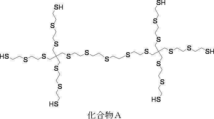
(実施例6)
実施例1で実施した銅配線基板を0.1mM Pentaerythritol tetrakis(2-mercaptoacetate)含有エタノール溶液に浸漬して、エタノールで洗浄する処理の代わりに、銅配線基板を0.1mM テトラキス-(7-メルカプト-2,5-ジチアヘプチル)メタン含有シクロヘキサノン溶液に10分間浸漬してシクロヘキサノン溶液で洗浄し、その後、得られた銅配線基板を5wt% ポリグリシジルメタクリレート含有シクロヘキサノン溶液(ポリグリシジルメタクリレートの数平均分子量:48000,Polymer source社製)に20分間浸漬してシクロヘキサノンで洗浄する処理を行った以外は、実施例1と同様の手順に従って、SRパターン付き銅配線基板を製造し、テープ剥離試験を行った。表1に結果をまとめて示す。
実施例1で実施した銅配線基板を0.1mM Pentaerythritol tetrakis(2-mercaptoacetate)含有エタノール溶液に浸漬して、エタノールで洗浄する処理の代わりに、銅配線基板を0.1mM テトラキス-(7-メルカプト-2,5-ジチアヘプチル)メタン含有シクロヘキサノン溶液に10分間浸漬してシクロヘキサノン溶液で洗浄し、その後、得られた銅配線基板を5wt% ポリグリシジルメタクリレート含有シクロヘキサノン溶液(ポリグリシジルメタクリレートの数平均分子量:48000,Polymer source社製)に20分間浸漬してシクロヘキサノンで洗浄する処理を行った以外は、実施例1と同様の手順に従って、SRパターン付き銅配線基板を製造し、テープ剥離試験を行った。表1に結果をまとめて示す。
(実施例7)
実施例1で使用した0.1mM Pentaerythritol tetrakis(2-mercaptoacetate)含有エタノール溶液の代わりに、テトラキス-(7-メルカプト-2,5-ジチアヘプチル)メタンと化合物Aとを含有するシクロヘキサノン溶液を使用し、洗浄溶剤としてエタノールの代わりにシクロヘキサノンを使用した以外は、実施例1と同様の手順に従って、SRパターン付き銅配線基板を製造し、テープ剥離試験を行った。表1に結果をまとめて示す。
なお、シクロヘキサン溶液中のテトラキス-(7-メルカプト-2,5-ジチアヘプチル)メタンと化合物Aと合計濃度は0.2mMで、両者はそれぞれ0.1mMずつ含まれていた。
実施例1で使用した0.1mM Pentaerythritol tetrakis(2-mercaptoacetate)含有エタノール溶液の代わりに、テトラキス-(7-メルカプト-2,5-ジチアヘプチル)メタンと化合物Aとを含有するシクロヘキサノン溶液を使用し、洗浄溶剤としてエタノールの代わりにシクロヘキサノンを使用した以外は、実施例1と同様の手順に従って、SRパターン付き銅配線基板を製造し、テープ剥離試験を行った。表1に結果をまとめて示す。
なお、シクロヘキサン溶液中のテトラキス-(7-メルカプト-2,5-ジチアヘプチル)メタンと化合物Aと合計濃度は0.2mMで、両者はそれぞれ0.1mMずつ含まれていた。
(実施例8)
実施例1で実施した銅配線基板を0.1mM Pentaerythritol tetrakis(2-mercaptoacetate)含有エタノール溶液に浸漬して、エタノールで洗浄する処理の代わりに、銅配線基板をテトラキス-(7-メルカプト-2,5-ジチアヘプチル)メタン含有シクロヘキサノン溶液に10分間浸漬してシクロヘキサノンで洗浄し、その後、得られた銅配線基板を0.1mM 化合物A含有シクロヘキサノン溶液に10分間浸漬してシクロヘキサノンで洗浄する処理を行った以外は、実施例1と同様の手順に従って、SRパターン付き銅配線基板を製造し、テープ剥離試験を行った。表1に結果をまとめて示す。
実施例1で実施した銅配線基板を0.1mM Pentaerythritol tetrakis(2-mercaptoacetate)含有エタノール溶液に浸漬して、エタノールで洗浄する処理の代わりに、銅配線基板をテトラキス-(7-メルカプト-2,5-ジチアヘプチル)メタン含有シクロヘキサノン溶液に10分間浸漬してシクロヘキサノンで洗浄し、その後、得られた銅配線基板を0.1mM 化合物A含有シクロヘキサノン溶液に10分間浸漬してシクロヘキサノンで洗浄する処理を行った以外は、実施例1と同様の手順に従って、SRパターン付き銅配線基板を製造し、テープ剥離試験を行った。表1に結果をまとめて示す。
(実施例9)
実施例1で実施した銅配線基板を0.1mM Pentaerythritol tetrakis(2-mercaptoacetate)含有エタノール溶液に浸漬して、エタノールで洗浄する処理の代わりに、以下の処理Xを行った以外は、実施例1と同様の手順に従って、SRパターン付き銅配線基板を製造し、テープ剥離試験を行った。表1に結果をまとめて示す。
(処理X)
銅配線基板を0.1mM テトラキス-(7-メルカプト-2,5-ジチアヘプチル)メタン含有シクロヘキサノン溶液に10分間浸漬して、シクロヘキサノンで洗浄し、その後、得られた銅配線基板を5wt% ポリグリシジルメタクリレート含有シクロヘキサノン溶液(ポリグリシジルメタクリレートの数平均分子量:48000,Polymer source社製)に20分間浸漬してシクロヘキサノンで洗浄した。さらに、得られた銅配線基板を100mM テトラキス-(7-メルカプト-2,5-ジチアヘプチル)メタン含有シクロヘキサノン溶液に10分間浸漬してシクロヘキサノンで洗浄し、その後、得られた銅配線基板を5wt% ポリグリシジルメタクリレート含有シクロヘキサノン溶液(ポリグリシジルメタクリレートの数平均分子量:48000,Polymer source社製)に30分間浸漬してシクロヘキサノンで洗浄した。
実施例1で実施した銅配線基板を0.1mM Pentaerythritol tetrakis(2-mercaptoacetate)含有エタノール溶液に浸漬して、エタノールで洗浄する処理の代わりに、以下の処理Xを行った以外は、実施例1と同様の手順に従って、SRパターン付き銅配線基板を製造し、テープ剥離試験を行った。表1に結果をまとめて示す。
(処理X)
銅配線基板を0.1mM テトラキス-(7-メルカプト-2,5-ジチアヘプチル)メタン含有シクロヘキサノン溶液に10分間浸漬して、シクロヘキサノンで洗浄し、その後、得られた銅配線基板を5wt% ポリグリシジルメタクリレート含有シクロヘキサノン溶液(ポリグリシジルメタクリレートの数平均分子量:48000,Polymer source社製)に20分間浸漬してシクロヘキサノンで洗浄した。さらに、得られた銅配線基板を100mM テトラキス-(7-メルカプト-2,5-ジチアヘプチル)メタン含有シクロヘキサノン溶液に10分間浸漬してシクロヘキサノンで洗浄し、その後、得られた銅配線基板を5wt% ポリグリシジルメタクリレート含有シクロヘキサノン溶液(ポリグリシジルメタクリレートの数平均分子量:48000,Polymer source社製)に30分間浸漬してシクロヘキサノンで洗浄した。
(比較例1)
実施例1で使用した0.1mM Pentaerythritol tetrakis(2-mercaptoacetate)含有エタノール溶液に10分間浸漬する代わりに、0.1mM 16-amino-1-hexadecanethiol含有エタノール溶液に60分間浸漬した以外は、実施例1と同様の手順に従って、SRパターン付き銅配線基板を製造し、テープ剥離試験を行った。表1に結果をまとめて示す。
なお、16-amino-1-hexadecanethiolのチオール当量(g/eq)は274であり、分子量は274であり、硫黄原子含有量は12wt%であった。
実施例1で使用した0.1mM Pentaerythritol tetrakis(2-mercaptoacetate)含有エタノール溶液に10分間浸漬する代わりに、0.1mM 16-amino-1-hexadecanethiol含有エタノール溶液に60分間浸漬した以外は、実施例1と同様の手順に従って、SRパターン付き銅配線基板を製造し、テープ剥離試験を行った。表1に結果をまとめて示す。
なお、16-amino-1-hexadecanethiolのチオール当量(g/eq)は274であり、分子量は274であり、硫黄原子含有量は12wt%であった。
(比較例2)
実施例1で使用した0.1mM Pentaerythritol tetrakis(2-mercaptoacetate)含有エタノール溶液に10分間浸漬する代わりに、0.1mM 1,10-デカンジチオール含有エタノール溶液に60分間浸漬した以外は、実施例1と同様の手順に従って、SRパターン付き銅配線基板を製造し、テープ剥離試験を行った。表1に結果をまとめて示す。
なお、1,10-デカンジチオールのチオール当量(g/eq)は103であり、分子量は206であり、硫黄原子含有量は31wt%であった。
実施例1で使用した0.1mM Pentaerythritol tetrakis(2-mercaptoacetate)含有エタノール溶液に10分間浸漬する代わりに、0.1mM 1,10-デカンジチオール含有エタノール溶液に60分間浸漬した以外は、実施例1と同様の手順に従って、SRパターン付き銅配線基板を製造し、テープ剥離試験を行った。表1に結果をまとめて示す。
なお、1,10-デカンジチオールのチオール当量(g/eq)は103であり、分子量は206であり、硫黄原子含有量は31wt%であった。
(比較例3)
実施例1で使用した0.1mM Pentaerythritol tetrakis(2-mercaptoacetate)含有エタノール溶液に10分間浸漬する代わりに、0.1mM チオシアヌル酸含有エタノール溶液に60分間浸漬した以外は、実施例1と同様の手順に従って、SRパターン付き銅配線基板を製造し、テープ剥離試験を行った。表1に結果をまとめて示す。
なお、チオシアヌル酸のチオール当量(g/eq)は59であり、分子量は177であり、硫黄原子含有量は54wt%であった。
実施例1で使用した0.1mM Pentaerythritol tetrakis(2-mercaptoacetate)含有エタノール溶液に10分間浸漬する代わりに、0.1mM チオシアヌル酸含有エタノール溶液に60分間浸漬した以外は、実施例1と同様の手順に従って、SRパターン付き銅配線基板を製造し、テープ剥離試験を行った。表1に結果をまとめて示す。
なお、チオシアヌル酸のチオール当量(g/eq)は59であり、分子量は177であり、硫黄原子含有量は54wt%であった。
(比較例4)
実施例1で使用した0.1mM Pentaerythritol tetrakis(2-mercaptoacetate)含有エタノール溶液の代わりに、0.1mM ベンゼントリチオール含有エタノール溶液を使用した以外は、実施例1と同様の手順に従って、SRパターン付き銅配線基板を製造し、テープ剥離試験を行った。表1に結果をまとめて示す。
なお、ベンゼントリチオールのチオール当量(g/eq)は58であり、分子量は174であり、硫黄原子含有量は55wt%であった。
実施例1で使用した0.1mM Pentaerythritol tetrakis(2-mercaptoacetate)含有エタノール溶液の代わりに、0.1mM ベンゼントリチオール含有エタノール溶液を使用した以外は、実施例1と同様の手順に従って、SRパターン付き銅配線基板を製造し、テープ剥離試験を行った。表1に結果をまとめて示す。
なお、ベンゼントリチオールのチオール当量(g/eq)は58であり、分子量は174であり、硫黄原子含有量は55wt%であった。
(比較例5)
実施例1で使用した0.1mM Pentaerythritol tetrakis(2-mercaptoacetate)含有エタノール溶液の代わりに、0.1mM Trimethylolpropane tris(3-mercaptopropionate)含有エタノール溶液を使用した以外は、実施例1と同様の手順に従って、SRパターン付き銅配線基板を製造し、テープ剥離試験を行った。表1に結果をまとめて示す。
なお、Trimethylolpropane tris(3-mercaptopropionate)のチオール当量(g/eq)は133であり、分子量は398であり、硫黄原子含有量は24wt%であった。
実施例1で使用した0.1mM Pentaerythritol tetrakis(2-mercaptoacetate)含有エタノール溶液の代わりに、0.1mM Trimethylolpropane tris(3-mercaptopropionate)含有エタノール溶液を使用した以外は、実施例1と同様の手順に従って、SRパターン付き銅配線基板を製造し、テープ剥離試験を行った。表1に結果をまとめて示す。
なお、Trimethylolpropane tris(3-mercaptopropionate)のチオール当量(g/eq)は133であり、分子量は398であり、硫黄原子含有量は24wt%であった。
(比較例6)
実施例1で使用した0.1mM Pentaerythritol tetrakis(2-mercaptoacetate)含有エタノール溶液に10分浸漬する代わりに、10mM (3-メルカプトプロピル)トリメトキシシラン含有エタノール溶液に5分浸漬した以外は、実施例1と同様の手順に従って、SRパターン付き銅配線基板を製造し、テープ剥離試験を行った。表1に結果をまとめて示す。
なお、(3-メルカプトプロピル)トリメトキシシランのチオール当量(g/eq)は196であり、分子量は196であり、硫黄原子含有量は16wt%であった。
実施例1で使用した0.1mM Pentaerythritol tetrakis(2-mercaptoacetate)含有エタノール溶液に10分浸漬する代わりに、10mM (3-メルカプトプロピル)トリメトキシシラン含有エタノール溶液に5分浸漬した以外は、実施例1と同様の手順に従って、SRパターン付き銅配線基板を製造し、テープ剥離試験を行った。表1に結果をまとめて示す。
なお、(3-メルカプトプロピル)トリメトキシシランのチオール当量(g/eq)は196であり、分子量は196であり、硫黄原子含有量は16wt%であった。
[実施例B]
実施例1でコア基板作製の際に行われた粗化処理剤を用いた銅パターン表面の表面処理を実施することなく、コア基板Bを作製した。得られた銅配線基板(コア基板B)の銅配線の厚みは15μmで、銅配線の表面粗さRzはRz=0.2μmであった。
該コア基板Bを使用して、上記実施例4~9と同様の手順に従って、SRパターン付き銅配線基板を製造し、テープ剥離試験を行った。表1に結果をまとめて示す。
実施例1でコア基板作製の際に行われた粗化処理剤を用いた銅パターン表面の表面処理を実施することなく、コア基板Bを作製した。得られた銅配線基板(コア基板B)の銅配線の厚みは15μmで、銅配線の表面粗さRzはRz=0.2μmであった。
該コア基板Bを使用して、上記実施例4~9と同様の手順に従って、SRパターン付き銅配線基板を製造し、テープ剥離試験を行った。表1に結果をまとめて示す。
なお、上記実施例1~9、および、比較例1~6で得られたチオール化合物で処理された銅配線基板をXPS測定したところ、銅配線上に硫黄原子の存在が確認され、チオール化合物が銅配線に結合していることが確認された。
実施例1~9にて銅配線上に形成されたチオール化合物の層の厚みは上記XPS測定結果より、いずれも0.1~2nm程度であった。また、実施例6および9では、チオール化合物の層とエポキシ樹脂層との積層構造が形成され、形成されたエポキシ樹脂層の厚みは10~100nm程度であった。
実施例1~9にて銅配線上に形成されたチオール化合物の層の厚みは上記XPS測定結果より、いずれも0.1~2nm程度であった。また、実施例6および9では、チオール化合物の層とエポキシ樹脂層との積層構造が形成され、形成されたエポキシ樹脂層の厚みは10~100nm程度であった。
以下の表1中、「樹脂接触工程」欄は、上述した樹脂接触工程を実施した場合を「有」、実施しなかった場合を「-」と表記した。
また、以下の表1中「コア基板A」欄は、コア基板Aを使用した実施例Aの結果に該当し、「コア基板B」欄は、コア基板Bを使用した実施例Bの結果に該当する。「コア基板A」欄および「コア基板B」欄中、「-」は未実施を意味する。
また、以下の表1中「コア基板A」欄は、コア基板Aを使用した実施例Aの結果に該当し、「コア基板B」欄は、コア基板Bを使用した実施例Bの結果に該当する。「コア基板A」欄および「コア基板B」欄中、「-」は未実施を意味する。

表1に示すように、本発明の製造方法により得られたプリント配線基板においては、絶縁層の密着性に優れていた。特に、実施例4~9で示されるように、硫黄原子含有量が35wt%以上のチオール化合物を使用した場合、より表面粗さRzが小さい銅配線を有するコア基板Bに対しても、絶縁層が優れた接着性を示すことが確認された。
一方、比較例1に示すようにチオール基を有さない化合物、または、比較例2~6に示すようにチオール基を2~3個有するチオール化合物を使用した場合、絶縁層の密着性に劣ることが確認された。
特に、比較例3の態様は、特許文献1の態様に該当し、従来技術では所望の効果が得られないことが確認された。
一方、比較例1に示すようにチオール基を有さない化合物、または、比較例2~6に示すようにチオール基を2~3個有するチオール化合物を使用した場合、絶縁層の密着性に劣ることが確認された。
特に、比較例3の態様は、特許文献1の態様に該当し、従来技術では所望の効果が得られないことが確認された。
<実施例10>
実施例4で絶縁層として使用した太陽インキ社製 PFR-800の代わりに味の素ファインテクノ(株)製、ABF GX-13をラミネートして、絶縁層付き銅配線基板を製造した。次に、レーザー加工により、絶縁層のパターン(L字パターン)(絶縁樹脂層の層厚:35μm)を作製し、さらに、レーザー加工で生じた残渣をデスミア処理により除去した。その後、上記Niめっき処理を行い、さらにゴブライトTSB-72(上村工業社製、液温80℃)に配線基板を5分間浸漬し、Auめっき処理(厚み30nm)を行った。なお、上記絶縁層には、無機フィラー(シリカ)が含まれていた。その後、絶縁層付き銅配線基板に対して、サーマルサイクル試験(-65℃で30分と150℃で30分の繰り返しを1000サイクル)を行い、テープ剥離試験を行った。表2に結果をまとめて示す。
なお、実施例10では、コア基板Bを使用した。
実施例4で絶縁層として使用した太陽インキ社製 PFR-800の代わりに味の素ファインテクノ(株)製、ABF GX-13をラミネートして、絶縁層付き銅配線基板を製造した。次に、レーザー加工により、絶縁層のパターン(L字パターン)(絶縁樹脂層の層厚:35μm)を作製し、さらに、レーザー加工で生じた残渣をデスミア処理により除去した。その後、上記Niめっき処理を行い、さらにゴブライトTSB-72(上村工業社製、液温80℃)に配線基板を5分間浸漬し、Auめっき処理(厚み30nm)を行った。なお、上記絶縁層には、無機フィラー(シリカ)が含まれていた。その後、絶縁層付き銅配線基板に対して、サーマルサイクル試験(-65℃で30分と150℃で30分の繰り返しを1000サイクル)を行い、テープ剥離試験を行った。表2に結果をまとめて示す。
なお、実施例10では、コア基板Bを使用した。
<比較例7>
実施例10で、チオール化合物で処理せずに、同様の手順で、テープ剥離試験を行った。表2に結果をまとめて示す。
実施例10で、チオール化合物で処理せずに、同様の手順で、テープ剥離試験を行った。表2に結果をまとめて示す。
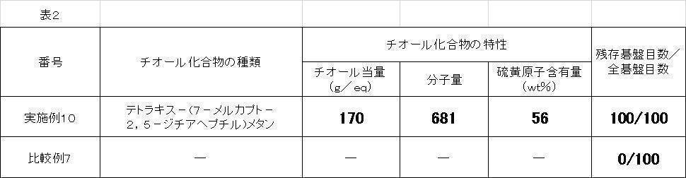
上記表2に示すように、絶縁層の種類を変更した実施例10においても、絶縁層の優れた密着性が確認された。
一方、比較例7に示すように、チオール化合物の層が介在していない場合、絶縁層の密着性が劣っていた。
一方、比較例7に示すように、チオール化合物の層が介在していない場合、絶縁層の密着性が劣っていた。
<実施例11>
シリコン基板上に銀を蒸着し、L/S=1000μm/100μmの銀配線を備えるコア基板を形成した。得られた銀配線基板の銀配線の厚みは0.3μm、銀配線の表面粗さRzはRz=0.02μmであった。
次に、得られた銀配線基板を0.1mM テトラキス-(7-メルカプト-2,5-ジチアヘプチル)メタン含有シクロヘキサノン溶液に20分間浸漬し、その後、洗浄溶剤としてシクロへキノンを使用して銀配線基板を洗浄し、さらに水で洗浄した後、室温で乾燥させた。
その後、チオール化合物で処理された銀配線基板上に絶縁層(太陽インキ社製 PFR-800)をラミネートし、その後パターンマスク(L字パターン)越しに露光し、現像後、ベークし、さらに露光を行って、SR(ソルダーレジスト)パターンを銀配線基板上に(絶縁層の層厚:30μm)を作製した。得られたSRパターン付き銀配線基板に関して、湿潤環境下(温度130℃、湿度85%RH、圧力1.2atm)(使用装置:espec社製、EHS-221MD)に100hr放置した後、サンプルを取り出し、上記テープ剥離試験を行った。表3に結果をまとめて示す。
シリコン基板上に銀を蒸着し、L/S=1000μm/100μmの銀配線を備えるコア基板を形成した。得られた銀配線基板の銀配線の厚みは0.3μm、銀配線の表面粗さRzはRz=0.02μmであった。
次に、得られた銀配線基板を0.1mM テトラキス-(7-メルカプト-2,5-ジチアヘプチル)メタン含有シクロヘキサノン溶液に20分間浸漬し、その後、洗浄溶剤としてシクロへキノンを使用して銀配線基板を洗浄し、さらに水で洗浄した後、室温で乾燥させた。
その後、チオール化合物で処理された銀配線基板上に絶縁層(太陽インキ社製 PFR-800)をラミネートし、その後パターンマスク(L字パターン)越しに露光し、現像後、ベークし、さらに露光を行って、SR(ソルダーレジスト)パターンを銀配線基板上に(絶縁層の層厚:30μm)を作製した。得られたSRパターン付き銀配線基板に関して、湿潤環境下(温度130℃、湿度85%RH、圧力1.2atm)(使用装置:espec社製、EHS-221MD)に100hr放置した後、サンプルを取り出し、上記テープ剥離試験を行った。表3に結果をまとめて示す。
<比較例8>
実施例11において、チオール化合物で処理せずに、同様の手順で湿潤環境下に100hr放置した後、サンプルを取り出し、上記テープ剥離試験を行った。表3に結果をまとめて示す。
実施例11において、チオール化合物で処理せずに、同様の手順で湿潤環境下に100hr放置した後、サンプルを取り出し、上記テープ剥離試験を行った。表3に結果をまとめて示す。
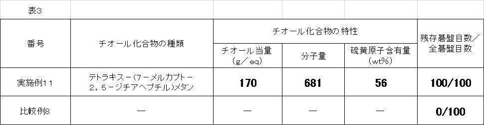
表3に示すように、金属配線として銀配線を用いた場合においても、本発明のプリント配線基板は、絶縁層の優れた密着性が確認された。
一方、比較例8に示すように、チオール化合物の層が介在していない場合、絶縁層の密着性が劣っていた。
一方、比較例8に示すように、チオール化合物の層が介在していない場合、絶縁層の密着性が劣っていた。
10:コア基板
12:絶縁基板
14:金属配線
16:チオール化合物の層
18:金属配線の表面に結合したチオール化合物の層
20:絶縁層
30:プリント配線基板
40:他の絶縁基板
50:他の金属配線
12:絶縁基板
14:金属配線
16:チオール化合物の層
18:金属配線の表面に結合したチオール化合物の層
20:絶縁層
30:プリント配線基板
40:他の絶縁基板
50:他の金属配線
Claims (10)
- 絶縁基板と、前記絶縁基板上に配置される金属配線と、前記金属配線上に配置される絶縁層とを備えるプリント配線基板であって、
前記金属配線と前記絶縁層との界面に式(1)で表される官能基を4つ以上有するチオール化合物の層が介在する、プリント配線基板。

- 前記チオール化合物のチオール当量(g/eq)が2100以下である、請求項1に記載のプリント配線基板。
- 前記チオール化合物の分子量が8400以下である、請求項1または2に記載のプリント配線基板。
- 前記チオール化合物が、以下の式(3)で表されるチオール化合物である、請求項1~3のいずれかに記載のプリント配線基板。

- 絶縁基板と前記絶縁基板上に配置される金属配線とを有するコア基板と、式(1)で表される官能基を4つ以上有するチオール化合物を含む金属表面処理液とを接触させ、その後前記コア基板を溶剤で洗浄して、金属配線表面上に式(1)で表される官能基を4つ以上有するチオール化合物の層を形成する配線処理工程と、
前記配線処理工程後に、処理されたコア基板上に絶縁層を形成する絶縁層形成工程と、を備えるプリント配線基板の製造方法。

- 前記チオール化合物のチオール当量(g/eq)が2100以下である、請求項5に記載のプリント配線基板の製造方法。
- 前記チオール化合物の分子量が8400以下である、請求項5または6に記載のプリント配線基板の製造方法。
- 前記チオール化合物が、以下の式(3)で表されるチオール化合物である、請求項5~7のいずれかに記載のプリント配線基板の製造方法。

- 式(1)で表される官能基を4つ以上有するチオール化合物を含有する、プリント配線基板中の金属配線と絶縁層との密着性向上のため前記金属配線表面を処理するために用いられる、プリント配線基板用の金属表面処理液。

- 請求項1~4のいずれかに記載のプリント配線基板を有するICパッケージ基板。
Priority Applications (3)
| Application Number | Priority Date | Filing Date | Title |
|---|---|---|---|
| KR1020137025481A KR101593560B1 (ko) | 2011-03-30 | 2012-03-16 | 프린트 배선기판 및 그 제조방법, 그리고 금속 표면 처리액 |
| CN201280015917.8A CN103477728B (zh) | 2011-03-30 | 2012-03-16 | 印刷配线基板及其制造方法、印刷配线基板用的金属表面处理液以及集成电路封装基板 |
| US14/039,803 US9295149B2 (en) | 2011-03-30 | 2013-09-27 | Printed circuit board, manufacturing method therefor, and metal-surface treatment liquid |
Applications Claiming Priority (4)
| Application Number | Priority Date | Filing Date | Title |
|---|---|---|---|
| JP2011-076049 | 2011-03-30 | ||
| JP2011076049 | 2011-03-30 | ||
| JP2011-176961 | 2011-08-12 | ||
| JP2011176961 | 2011-08-12 |
Related Child Applications (1)
| Application Number | Title | Priority Date | Filing Date |
|---|---|---|---|
| US14/039,803 Continuation US9295149B2 (en) | 2011-03-30 | 2013-09-27 | Printed circuit board, manufacturing method therefor, and metal-surface treatment liquid |
Publications (1)
| Publication Number | Publication Date |
|---|---|
| WO2012132970A1 true WO2012132970A1 (ja) | 2012-10-04 |
Family
ID=46930703
Family Applications (1)
| Application Number | Title | Priority Date | Filing Date |
|---|---|---|---|
| PCT/JP2012/056904 Ceased WO2012132970A1 (ja) | 2011-03-30 | 2012-03-16 | プリント配線基板およびその製造方法、並びに、金属表面処理液 |
Country Status (6)
| Country | Link |
|---|---|
| US (1) | US9295149B2 (ja) |
| JP (1) | JP5683516B2 (ja) |
| KR (1) | KR101593560B1 (ja) |
| CN (1) | CN103477728B (ja) |
| TW (1) | TWI533768B (ja) |
| WO (1) | WO2012132970A1 (ja) |
Families Citing this family (7)
| Publication number | Priority date | Publication date | Assignee | Title |
|---|---|---|---|---|
| IN2014DN03390A (ja) * | 2011-10-03 | 2015-06-05 | Hitachi Chemical Co Ltd | |
| JP6472596B2 (ja) * | 2014-02-13 | 2019-02-20 | 日亜化学工業株式会社 | 発光装置及びその製造方法 |
| EP3158578B1 (en) | 2014-07-08 | 2024-01-10 | Canon Kabushiki Kaisha | Adhesion layer composition, method for forming film by nanoimprinting, methods for manufacturing optical component, circuit board and electronic apparatus |
| TWI540944B (zh) | 2014-07-14 | 2016-07-01 | 啟碁科技股份有限公司 | 基板結構的製造方法、基板結構以及金屬構件 |
| CN105307378B (zh) * | 2014-07-18 | 2018-10-19 | 启碁科技股份有限公司 | 基板结构的制造方法、基板结构以及金属构件 |
| KR101616077B1 (ko) * | 2015-09-23 | 2016-04-28 | 두두테크 주식회사 | 차량용 액셀러레이터 페달 액추에이터 인쇄회로기판의 제조 방법 |
| JP6402134B2 (ja) * | 2016-05-12 | 2018-10-10 | 株式会社タムラ製作所 | 水溶性プリフラックス、それを用いた表面処理方法 |
Citations (6)
| Publication number | Priority date | Publication date | Assignee | Title |
|---|---|---|---|---|
| JP2000156563A (ja) * | 1998-11-19 | 2000-06-06 | Matsushita Electric Ind Co Ltd | プリント配線基板 |
| JP2001203462A (ja) * | 2000-01-18 | 2001-07-27 | Toa Denka:Kk | プリント配線板の製造方法および多層プリント配線板 |
| JP2004277444A (ja) * | 2003-03-12 | 2004-10-07 | Ricoh Co Ltd | 導電性接着剤 |
| JP2009051936A (ja) * | 2007-08-27 | 2009-03-12 | Mitsubishi Rayon Co Ltd | 硬化性組成物及びその硬化物 |
| JP2010126572A (ja) * | 2008-11-26 | 2010-06-10 | Jsr Corp | プライマー組成物、プライマー層、及び積層体 |
| WO2011021363A1 (ja) * | 2009-08-19 | 2011-02-24 | 株式会社ブリヂストン | 光硬化性組成物 |
Family Cites Families (20)
| Publication number | Priority date | Publication date | Assignee | Title |
|---|---|---|---|---|
| US4598009A (en) * | 1984-09-13 | 1986-07-01 | Armstrong World Industries, Inc. | Embossed material and method for producing the same from a photocrosslinkable polyurethane |
| US5487792A (en) * | 1994-06-13 | 1996-01-30 | Midwest Research Institute | Molecular assemblies as protective barriers and adhesion promotion interlayer |
| JP4260258B2 (ja) * | 1998-12-25 | 2009-04-30 | 日鉱金属株式会社 | プリント基板用銅箔及びプリント基板 |
| JP2001160689A (ja) | 1999-12-02 | 2001-06-12 | Nippon Zeon Co Ltd | 多層回路基板 |
| TW540284B (en) * | 2001-09-05 | 2003-07-01 | Zeon Corp | Process for manufacturing multi-layer circuit substrate |
| US6951666B2 (en) * | 2001-10-05 | 2005-10-04 | Cabot Corporation | Precursor compositions for the deposition of electrically conductive features |
| EP1481796B1 (en) * | 2002-03-05 | 2015-08-19 | Hitachi Chemical Co., Ltd. | Metal foil with resin and metal-clad laminate, and printed wiring board using the same and method for production thereof |
| KR100627404B1 (ko) * | 2002-11-20 | 2006-09-21 | 가부시키가이샤 도모에가와 세이시쇼 | 가요성 금속적층체 및 내열성 접착제 조성물 |
| US7452574B2 (en) * | 2003-02-27 | 2008-11-18 | Molecular Imprints, Inc. | Method to reduce adhesion between a polymerizable layer and a substrate employing a fluorine-containing layer |
| US7661190B2 (en) * | 2003-03-04 | 2010-02-16 | Zeon Corporation | Process for producing multilayer printed wiring board |
| US6858527B2 (en) * | 2003-04-14 | 2005-02-22 | Intel Corporation | Method to increase electromigration resistance of copper using self-assembled organic thiolate monolayers |
| AT412094B (de) * | 2003-05-13 | 2004-09-27 | Austria Tech & System Tech | Verfahren zur beschichtung von rohlingen zur herstellung von gedruckten leiterplatten (pcb) |
| US20070269665A1 (en) * | 2003-05-20 | 2007-11-22 | Kaneka Corporation | Polyimide Resin Composition, Polymer Film Containing Polymide Resin and Laminate Using the Same, and Method for Manufacturing Printed Wiring Board |
| KR100581221B1 (ko) * | 2004-06-30 | 2006-05-22 | 삼성전자주식회사 | 테이프 배선 기판 제조 방법 |
| EP2015071A1 (en) * | 2007-07-13 | 2009-01-14 | FUJIFILM Corporation | Carrier, process for producing same, bioreactor, and chip for surface plasmon resonance analysis |
| WO2009057376A1 (ja) * | 2007-10-29 | 2009-05-07 | Hitachi Chemical Company, Ltd. | 回路接続材料、接続構造体及びその製造方法 |
| TWI453301B (zh) * | 2007-11-08 | 2014-09-21 | Enthone | 浸鍍銀塗層上的自組分子 |
| JP5365003B2 (ja) * | 2008-01-11 | 2013-12-11 | 横浜ゴム株式会社 | ハネムーン型接着剤組成物、実装基板の接着方法および実装基板組み立て体 |
| EP2257969B1 (en) * | 2008-02-28 | 2017-12-20 | 3M Innovative Properties Company | Methods of patterning a conductor on a substrate |
| US8901263B2 (en) * | 2008-12-11 | 2014-12-02 | 3M Innovative Properties Company | Amide-linked perfluoropolyether thiol compounds and processes for their preparation and use |
-
2012
- 2012-03-16 CN CN201280015917.8A patent/CN103477728B/zh not_active Expired - Fee Related
- 2012-03-16 KR KR1020137025481A patent/KR101593560B1/ko not_active Expired - Fee Related
- 2012-03-16 JP JP2012060145A patent/JP5683516B2/ja not_active Expired - Fee Related
- 2012-03-16 WO PCT/JP2012/056904 patent/WO2012132970A1/ja not_active Ceased
- 2012-03-22 TW TW101109779A patent/TWI533768B/zh not_active IP Right Cessation
-
2013
- 2013-09-27 US US14/039,803 patent/US9295149B2/en not_active Expired - Fee Related
Patent Citations (6)
| Publication number | Priority date | Publication date | Assignee | Title |
|---|---|---|---|---|
| JP2000156563A (ja) * | 1998-11-19 | 2000-06-06 | Matsushita Electric Ind Co Ltd | プリント配線基板 |
| JP2001203462A (ja) * | 2000-01-18 | 2001-07-27 | Toa Denka:Kk | プリント配線板の製造方法および多層プリント配線板 |
| JP2004277444A (ja) * | 2003-03-12 | 2004-10-07 | Ricoh Co Ltd | 導電性接着剤 |
| JP2009051936A (ja) * | 2007-08-27 | 2009-03-12 | Mitsubishi Rayon Co Ltd | 硬化性組成物及びその硬化物 |
| JP2010126572A (ja) * | 2008-11-26 | 2010-06-10 | Jsr Corp | プライマー組成物、プライマー層、及び積層体 |
| WO2011021363A1 (ja) * | 2009-08-19 | 2011-02-24 | 株式会社ブリヂストン | 光硬化性組成物 |
Also Published As
| Publication number | Publication date |
|---|---|
| US20140020932A1 (en) | 2014-01-23 |
| TW201242449A (en) | 2012-10-16 |
| KR20140019789A (ko) | 2014-02-17 |
| US9295149B2 (en) | 2016-03-22 |
| KR101593560B1 (ko) | 2016-02-15 |
| TWI533768B (zh) | 2016-05-11 |
| CN103477728B (zh) | 2016-05-18 |
| JP5683516B2 (ja) | 2015-03-11 |
| JP2013058725A (ja) | 2013-03-28 |
| CN103477728A (zh) | 2013-12-25 |
Similar Documents
| Publication | Publication Date | Title |
|---|---|---|
| JP5683516B2 (ja) | プリント配線基板およびその製造方法、並びに、金属表面処理液 | |
| JP5667927B2 (ja) | マイグレーション抑制層形成用処理液、および、マイグレーション抑制層を有する積層体の製造方法 | |
| JP6370836B2 (ja) | 表面処理剤、樹脂組成物およびそれらの利用 | |
| WO2012111375A1 (ja) | 多層基板の製造方法、デスミア処理方法 | |
| JP5719791B2 (ja) | プリント配線基板の製造方法 | |
| CN102415226B (zh) | 多层印刷电路板的制造方法 | |
| JP2008109087A (ja) | 半導体チップ搭載用基板及び前処理液 | |
| JP2012214872A (ja) | 金属膜を有する積層体の製造方法 | |
| JP5647967B2 (ja) | プリント配線基板の製造方法、プリント配線基板 | |
| JP6591284B2 (ja) | 金属の表面処理液、表面処理方法およびその利用 | |
| JP2012214895A (ja) | パターン状金属膜を有する積層体の製造方法、被めっき層形成用組成物 | |
| TW202523672A (zh) | 四唑化合物、該四唑化合物之合成方法及其利用 | |
| JP2012209392A (ja) | パターン状金属膜を有する積層体の製造方法、被めっき層形成用組成物 | |
| JP2013008961A (ja) | プリント配線基板、および、プリント配線基板を選択する方法 | |
| JP2012214889A (ja) | 金属膜を有する積層体およびその製造方法、並びに、パターン状金属膜を有する積層体およびその製造方法 | |
| JP2016211035A (ja) | 金属の表面処理方法及びその利用 | |
| JP2016204725A (ja) | 金属の表面処理方法及びその利用 | |
| JP2013125797A (ja) | 配線基板およびその製造方法、銀イオン拡散抑制層形成用水溶液 | |
| HK40114045A (zh) | 三唑化合物、该三唑化合物的合成方法、偶联剂和它们的用途 |
Legal Events
| Date | Code | Title | Description |
|---|---|---|---|
| 121 | Ep: the epo has been informed by wipo that ep was designated in this application |
Ref document number: 12763403 Country of ref document: EP Kind code of ref document: A1 |
|
| ENP | Entry into the national phase |
Ref document number: 20137025481 Country of ref document: KR Kind code of ref document: A |
|
| NENP | Non-entry into the national phase |
Ref country code: DE |
|
| 122 | Ep: pct application non-entry in european phase |
Ref document number: 12763403 Country of ref document: EP Kind code of ref document: A1 |