WO2012132737A1 - 裏面照射型固体撮像素子及びその製造方法並びに撮像装置 - Google Patents
裏面照射型固体撮像素子及びその製造方法並びに撮像装置 Download PDFInfo
- Publication number
- WO2012132737A1 WO2012132737A1 PCT/JP2012/055126 JP2012055126W WO2012132737A1 WO 2012132737 A1 WO2012132737 A1 WO 2012132737A1 JP 2012055126 W JP2012055126 W JP 2012055126W WO 2012132737 A1 WO2012132737 A1 WO 2012132737A1
- Authority
- WO
- WIPO (PCT)
- Prior art keywords
- imaging device
- state imaging
- photodiode
- layer
- surface side
- Prior art date
- Legal status (The legal status is an assumption and is not a legal conclusion. Google has not performed a legal analysis and makes no representation as to the accuracy of the status listed.)
- Ceased
Links
Images



Classifications
-
- H—ELECTRICITY
- H10—SEMICONDUCTOR DEVICES; ELECTRIC SOLID-STATE DEVICES NOT OTHERWISE PROVIDED FOR
- H10F—INORGANIC SEMICONDUCTOR DEVICES SENSITIVE TO INFRARED RADIATION, LIGHT, ELECTROMAGNETIC RADIATION OF SHORTER WAVELENGTH OR CORPUSCULAR RADIATION
- H10F39/00—Integrated devices, or assemblies of multiple devices, comprising at least one element covered by group H10F30/00, e.g. radiation detectors comprising photodiode arrays
- H10F39/10—Integrated devices
- H10F39/12—Image sensors
- H10F39/199—Back-illuminated image sensors
-
- H—ELECTRICITY
- H04—ELECTRIC COMMUNICATION TECHNIQUE
- H04N—PICTORIAL COMMUNICATION, e.g. TELEVISION
- H04N25/00—Circuitry of solid-state image sensors [SSIS]; Control thereof
- H04N25/10—Circuitry of solid-state image sensors [SSIS]; Control thereof for transforming different wavelengths into image signals
- H04N25/11—Arrangement of colour filter arrays [CFA]; Filter mosaics
- H04N25/13—Arrangement of colour filter arrays [CFA]; Filter mosaics characterised by the spectral characteristics of the filter elements
- H04N25/134—Arrangement of colour filter arrays [CFA]; Filter mosaics characterised by the spectral characteristics of the filter elements based on three different wavelength filter elements
-
- H—ELECTRICITY
- H04—ELECTRIC COMMUNICATION TECHNIQUE
- H04N—PICTORIAL COMMUNICATION, e.g. TELEVISION
- H04N25/00—Circuitry of solid-state image sensors [SSIS]; Control thereof
- H04N25/70—SSIS architectures; Circuits associated therewith
- H04N25/702—SSIS architectures characterised by non-identical, non-equidistant or non-planar pixel layout
-
- H—ELECTRICITY
- H10—SEMICONDUCTOR DEVICES; ELECTRIC SOLID-STATE DEVICES NOT OTHERWISE PROVIDED FOR
- H10F—INORGANIC SEMICONDUCTOR DEVICES SENSITIVE TO INFRARED RADIATION, LIGHT, ELECTROMAGNETIC RADIATION OF SHORTER WAVELENGTH OR CORPUSCULAR RADIATION
- H10F39/00—Integrated devices, or assemblies of multiple devices, comprising at least one element covered by group H10F30/00, e.g. radiation detectors comprising photodiode arrays
- H10F39/011—Manufacture or treatment of image sensors covered by group H10F39/12
-
- H—ELECTRICITY
- H10—SEMICONDUCTOR DEVICES; ELECTRIC SOLID-STATE DEVICES NOT OTHERWISE PROVIDED FOR
- H10F—INORGANIC SEMICONDUCTOR DEVICES SENSITIVE TO INFRARED RADIATION, LIGHT, ELECTROMAGNETIC RADIATION OF SHORTER WAVELENGTH OR CORPUSCULAR RADIATION
- H10F39/00—Integrated devices, or assemblies of multiple devices, comprising at least one element covered by group H10F30/00, e.g. radiation detectors comprising photodiode arrays
- H10F39/80—Constructional details of image sensors
- H10F39/805—Coatings
- H10F39/8053—Colour filters
-
- H—ELECTRICITY
- H10—SEMICONDUCTOR DEVICES; ELECTRIC SOLID-STATE DEVICES NOT OTHERWISE PROVIDED FOR
- H10F—INORGANIC SEMICONDUCTOR DEVICES SENSITIVE TO INFRARED RADIATION, LIGHT, ELECTROMAGNETIC RADIATION OF SHORTER WAVELENGTH OR CORPUSCULAR RADIATION
- H10F39/00—Integrated devices, or assemblies of multiple devices, comprising at least one element covered by group H10F30/00, e.g. radiation detectors comprising photodiode arrays
- H10F39/80—Constructional details of image sensors
- H10F39/806—Optical elements or arrangements associated with the image sensors
- H10F39/8063—Microlenses
Definitions
- the present invention relates to a back-illuminated solid-state imaging device, a manufacturing method thereof, and an imaging apparatus.
- a red detection pixel photodiode: photoelectric conversion element
- a green detection pixel and a blue detection pixel are provided on a semiconductor substrate.
- a microlens (top lens) is stacked on each pixel, and incident light collected by each microlens passes through a corresponding color filter and enters a pixel corresponding to the microlens.
- the light receiving area of each pixel is R pixel> G pixel> B pixel, and the area of the red (R) pixel that receives light having a long wavelength is increased. Therefore, color mixing and crosstalk are reduced.
- color mixing and crosstalk can be reduced by changing the size (light receiving area) of each pixel according to the wavelength of light to be received.
- the size of each pixel differs for each color of light received, characteristics (reading voltage) for reading a captured image signal from the pixel (photodiode), saturation characteristics of each pixel, etc. will differ for each color. Problems arise.
- An object of the present invention is to provide a back-illuminated solid-state imaging device, a manufacturing method thereof, and an imaging apparatus that can reduce crosstalk to adjacent pixels of a pixel that receives long-wavelength light without changing the readout characteristics and saturation characteristics of each pixel. About.
- a backside illuminated solid-state imaging device and a method of manufacturing the same according to the present invention include a semiconductor substrate in which each of a plurality of photodiodes arranged in a two-dimensional array is formed from the back side to the front side where light enters, A color filter that is stacked on the back side of the semiconductor substrate and separates light, and a light filter that is stacked on the back side of the color filter for each photodiode and collects incident light to enter the back side of the corresponding photodiode.
- a back-illuminated solid-state imaging device including a microlens and a signal reading unit that is formed on the front surface side of the semiconductor substrate and reads an imaging signal detected by the photodiode according to the amount of received light, and a method for manufacturing the same, Regardless of the color of light that is split by a color filter and incident on each photodiode, the surface of each photodiode And the area of the back side of the photodiode where the dispersed red light is incident is larger than the area of the back side of the photodiode where the green or blue light is incident It is characterized by forming in.
- the imaging apparatus of the present invention is characterized by mounting the above-described back-illuminated solid-state imaging device.
- FIG. 3A shows an example of the color filter provided in the back surface side of the back surface irradiation type solid-state image sensor shown in FIG. 3
- FIG. 3B is a schematic cross-sectional view (FIG. 3A) and a comparative view (FIG. 3B) taken along the line IIIA-IIIA in FIG.
- FIG. 3A It is a figure which shows the mask used when manufacturing n area
- FIG. It is a cross-sectional schematic diagram of embodiment which replaces 3A embodiment.
- FIG. It is a figure which shows the mask of embodiment which replaces 4A.
- FIG. 1 is a functional block configuration diagram of a digital camera (imaging device) equipped with a solid-state imaging device according to an embodiment of the present invention.
- the digital camera 10 includes a photographic optical system 21 and an image sensor chip 22 arranged at a subsequent stage of the photographic optical system 21.
- the photographing optical system 21 includes a photographing lens 21a, a diaphragm 21b, a mechanical shutter (not shown), and the like. Some models do not have a mechanical shutter.
- the signal reading unit automatically adjusts the gain of the back-illuminated solid-state image pickup device 22a for color image pickup such as the CCD type or the CMOS type and the analog image data output from the back-side irradiation type solid-state image pickup device 22a.
- AGC analog signal processing unit
- AFE analog signal processing unit 22b that performs analog processing such as correlated double sampling processing
- a / analog / digital conversion unit
- the digital camera 10 further includes a driving unit (including a timing generator TG) 23 that controls driving of the solid-state imaging device 22a, the analog signal processing unit 22b, and the A / D 22c in accordance with an instruction from a system control unit (CPU) 29 described later. And a flash 25 that emits light in response to an instruction from the CPU 29.
- the drive unit 23 may be mounted together in the image sensor chip 22 in some cases.
- the digital camera 10 of this embodiment further includes a digital signal processing unit 26 that takes in digital image data output from the A / D 22c and performs known image processing such as interpolation processing, white balance correction, and RGB / YC conversion processing, and an image.
- the compression / decompression processing unit 27 that compresses data into JPEG format image data or the like, and the display unit 28 that displays menus and displays through images and captured images, and the entire digital camera.
- a system control unit (CPU) 29 for controlling, an internal memory 30 such as a frame memory, and a media interface (I / F) unit 31 for performing interface processing between a recording medium 32 for storing JPEG image data and the like; Are connected to each other, and the system controller 29 receives instructions from the user. It is connected with an operation unit 33 that performs.
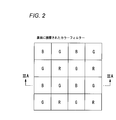
- FIG. 2 is a diagram illustrating a partial color filter array on the back-side light-receiving surface of the back-illuminated solid-state imaging device 22a shown in FIG.
- the color filters RGB of the three primary colors are arranged in a Bayer array.
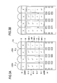
- FIG. 3A is a schematic cross-sectional view taken along the line IIIA-IIIA in FIG.
- color filters (R, G, B) 52 corresponding to each pixel are stacked on the back side of the p-type semiconductor substrate 51 (the light incident side is the back side).
- a microlens 53 corresponding to each pixel is stacked on the color filter 52.
- the microlens 53 corresponding to each pixel is formed in the same shape and size by the same manufacturing process.
- a p-type semiconductor substrate 51 having a thickness of 3 to 4 ⁇ m is used, but a substrate having a thickness other than this may be used.
- a signal reading unit 54 (signal reading circuit) that reads a captured image signal from each pixel is formed. Since the back-illuminated solid-state imaging device 22a in the illustrated example is a CMOS type, three wiring layers of the signal readout unit 54 formed of a CMOS transistor are illustrated.
- a transparent planarization film 55 is laminated between the color filter 52 and the microlens 53, and a transparent planarization film, an oxide film 56, and the like are provided between the p-type semiconductor substrate 51 and the color filter 52.
- An insulating layer 57 and the like are also provided on the surface side of the p-type semiconductor substrate 51, and a surface high-concentration p layer (not shown) for preventing white scratches due to dark current is provided.
- an n region 60 is provided for each pixel. Is provided.
- the n region 60 is composed of four layers of n regions 60-1, 60-2, 60-3, and 60-4 in which the impurity concentration decreases in order from the front surface side to the back surface side of the semiconductor substrate 51.
- the ion implantation concentration of the n-type impurity per unit area of the first layer 60-1 is 1e12 / cm 2 or more, and the ion implantation concentration of the second to fourth layers is less than 1e12 / cm 2 . Is good.
- an n region 60 is provided, but in this embodiment, only the structure of the n region (reference numeral is “60R”) of the pixel in which the R filter is stacked, The structure is different from that of the n region 60 of the pixel having other B filters and G filters.
- the n region 60R in the pixel in which the R filters are stacked is also composed of four layers (60R-1, 60R-2, 60) in which the n-type impurity concentration decreases in order from the front surface side to the back surface side of the semiconductor substrate 51. 60R-3, 60R-4) structure.
- the area of the first layer 60R-1 having the highest n-type impurity concentration from the surface side of the n region 60R that is, the area of the n region layer 60R-1 from which the imaged image signal is read (areas viewed from the front side and the back side of the semiconductor substrate) )
- the area of the first layer 60-1 from the surface side of the n region 60 of the other color are formed to have the same area.
- the areas of the second layers 60R-2 and 60-2 from the surface side are also formed to have the same area as the first layers 60R-1 and 60-1.
- the areas of the layers 60R-3 and 60R-4 having the low impurity concentration in the third and fourth layers from the surface side of the n region 60R are divided into three layers from the surface side of the n region 60 of other colors. It is formed wider than the first and fourth layers 60-3 and 60-4.
- FIG. 3B is shown in FIG. 3A is shown for comparison with FIG. In 3B, all the n regions of the R filter mounted pixels have the same area and the same area as other color pixels.
- the condensing point of each microlens 53 is a range between the back surface side surface of the semiconductor substrate 51 and a half depth on the back surface side of the fourth layers 60-4 and 60R-4 of the n regions 60 and 60R. Since the area of the fourth layer 60R-4 is larger than that of the adjacent pixel, the R light leaks to the adjacent pixel when the R light is condensed on the n region layer 60-4. Crosstalk can be reduced.
- the signal charges (electrons) photoelectrically converted by the fourth and third layers 60R-4 and 60R-3 having a low impurity concentration move to the layers 60R-2 and 60R-1 having a high impurity concentration to move to one layer. Accumulated in the eye layer 60R-4.
- the area of the first layer 60-1 in the other n region 60 will be different. End up. As a result, there arises a problem that the readout characteristics and saturation characteristics when the captured image signal is read out from the first layer are different between the R filter laminated pixel and the other color (G, B) filter laminated pixels.
- the areas of the fourth layer 60R-4 and the third layer 60R-3 that receive incident light are made wider than the blue detection pixel and the green detection pixel, while the red color for reading the captured image signal. Since the area of the first layer 60R-1 of the detection pixel is the same as that of the first layer 60-1 of the other color, the readout characteristics, saturation characteristics, and the like are the same. Further, as described above, since the impurity concentration of the layers 60R-4 and 60R-3 which are far from the first layer 60R-1 for signal readout and whose area is expanded is reduced, the readout characteristics, saturation characteristics, etc. are improved. The effect on the first layer is reduced.
- the influence of the fourth layer 60R-4 which has a large area, extends to the first layer 60R-1.
- the reading characteristics and saturation characteristics are the same as those of the first layer 60-1 for other colors.
- FIG. An open rectangular portion in the figure is a through hole, and an n-type impurity is implanted from the surface side through this hole.
- RGB described in the rectangular portion represents the corresponding color filter RGB.
- FIG. 4A is a mask 65 used when manufacturing the shallow layers 60-4, 60-3, 60R-4, and 60R-3 from the back side of the semiconductor substrate 51.
- FIG. Reference numeral 4B denotes a mask 66 used when manufacturing the deep layers 60-1, 60-2, 60R-1, and 60R-2 from the back side of the semiconductor substrate 51.
- ion implantation is performed from the surface side of the semiconductor substrate 51, when manufacturing the layers 60-1 and 60R-1 closest to the surface side, low energy and high concentration impurities are implanted and the deepest layer from the surface is formed.
- 60-4 and 60R-4 high energy and low concentration impurities are implanted.
- the aperture areas of the RGB holes 66R, 66G, and 66B are the same, but in the mask 65, the R hole 65R is expanded compared to the aperture areas of the GB holes 65G and 65B. ing. As a result, the area of the third and fourth layers of the n region 60R of the red detection pixel can be made larger than the areas of the first and second layers.
- FIG. 5 shows FIG. It is a cross-sectional schematic diagram of the backside illumination type solid-state image sensor which concerns on another embodiment of this invention which replaces 3A embodiment.
- FIG. 5 The difference from the embodiment of 3A is that the area of the second layer 60R-2 of the n region 60R is also widened, and only the first layer 60R-1 has the same area as the areas of the other n regions 60.
- the back-illuminated solid-state image sensor has a higher proportion of photoelectric conversion elements in the light-receiving surface than the front-illuminated solid-state image sensor in which the signal reading unit is also provided on the side where the light-receiving surface of the photodiode (pixel) is provided.
- the light receiving sensitivity increases, but the semiconductor substrate becomes thick. Since the penetration distance of incident light into the semiconductor substrate penetrates deeper as the wavelength increases, the back-illuminated type in particular has a problem of crosstalk of red light as compared with the front-side illuminated type.
- FIG. If the area of the n region 60R is expanded from the back side light incident surface of the semiconductor substrate to a deep position as in the embodiment of FIG. 3A or FIG. 5, the red light that is weakly absorbed in the semiconductor substrate passes the condensing point. Even if it spreads in the semiconductor substrate, red light is absorbed in the n region 60R and can be photoelectrically converted, so that crosstalk and color mixing can be reduced.
- FIG. 6 shows FIG. It is a figure which shows the mask which concerns on another embodiment of this invention which replaces 4A embodiment.
- the light receiving area of the photodiode that receives red light out of the incident light is made larger than the light receiving area of the photodiode that receives the other colors, and the area of the photodiode that reads the captured image signal is set for each color. Therefore, the crosstalk of red light can be reduced without changing the readout characteristics, saturation characteristics, etc. for each color.
- each pixel photodiode
- a square lattice an example of a two-dimensional array arrangement
- a color filter is Bayer arranged
- the present invention is not limited to this, and can also be applied to a so-called honeycomb pixel array in which odd-numbered pixel lines are shifted by 1/2 pixel pitch with respect to even-numbered pixel lines. Applicable to stripes and horizontal stripes.
- FIG. 3A the areas of the third layer 60R-3 and the fourth layer 60R-4 are expanded, but the effect of the present invention can be obtained even if the area of only the fourth layer 60R-4 is expanded. is there.
- the n regions 60 and 60R have a four-layer structure, but a two-layer structure, a three-layer structure, or other structures may be used, and the light incident surface of the photodiode that receives red light.
- the area of the side layer wider than that of other colors, the same effect as that of the above-described embodiment can be obtained.
- each of a plurality of photodiodes arranged in a two-dimensional array is formed from the backside to the frontside where light is incident.
- a back-illuminated solid-state imaging device including a microlens that is incident on the back surface side, and a signal reading unit that is formed on the front surface side of the semiconductor substrate and that reads an imaging signal detected by the photodiode according to the amount of received light, and its manufacture
- a method Regardless of the color of the light that is split by the color filter and incident on each photodiode, the surface area of each photodiode is formed to have the same area, and the split red light is incident on the photodiode.
- the area on the back surface side of the photodiode is formed larger than the area on the back surface side of the photodiode on which green or blue light is incident.
- the area on the back surface side of the photodiode on which the green light is incident is the area on the back surface side of the photodiode on which the blue light is incident. It is characterized by being formed in a larger area.
- the backside illuminated solid-state imaging device and the photodiodes of the manufacturing method thereof according to the embodiment are characterized in that the backside impurity concentration is lower than the frontside impurity concentration.
- each of the photodiodes of the back-illuminated solid-state imaging device and the manufacturing method thereof according to the embodiment is characterized in that it is formed of a plurality of layers in which the impurity concentration sequentially increases from the back surface side to the front surface side.
- the plurality of layers of the backside illuminated solid-state imaging device and the manufacturing method thereof according to the embodiment are configured by at least three layers, and the layer having the large area is only the layer on the backside most. To do.
- the plurality of layers of the back-illuminated solid-state imaging device and the manufacturing method thereof according to the embodiment are configured by at least three layers, and the layer having the large area is a layer other than the layer on the most surface side.
- the backside illumination type solid-state imaging device and the manufacturing method thereof according to the embodiment are characterized in that the thickness of the layer on the most surface side among the plurality of layers is formed to be at least 1 ⁇ m or more.
- the backside illuminated solid-state imaging device and the manufacturing method thereof according to the embodiment are characterized in that the most surface layer of the photodiode is formed with an ion implantation concentration of 1e12 / cm 2 or more per unit area. To do.
- the layers other than the most surface layer of the photodiode are formed with an ion implantation concentration of less than 1e12 / cm 2 per unit area. It is characterized by.
- the imaging apparatus according to the embodiment is characterized in that the back-illuminated solid-state imaging device described above is mounted.
- the back-illuminated solid-state imaging device can reduce the crosstalk of red light in particular. Therefore, a digital camera, a mobile phone with a camera, an electronic device with a camera, and an imaging device for an endoscope. It is useful when applied to the above.
- This application is based on Japanese Patent Application No. 2011-67891 filed on Mar. 25, 2011, the contents of which are incorporated herein by reference.
- Imaging device (digital camera) 22 Image sensor chip 22a Back-illuminated solid-state image sensor 51 p-type semiconductor substrate 52 color filter layer 53 microlens 54 signal readout unit 60 n region 60-1 first layer (impurity concentration is high) 60-2 Second layer (impurity concentration is high or low) 60-3 3rd layer (impurity concentration is low and high) 60-4 4th layer (impurity concentration is low and low) 60R n region 60R-1 first layer of red detection pixel (impurity concentration is high) 60R-2 Second layer (impurity concentration is high or low) 60R-3 3rd layer (impurity concentration is low and high) 60R-4 4th layer (impurity concentration is low and low) 65, 66, 67 Mask 65R, 65G, 65B Mask hole 66R, 66G, 66B Mask hole 67R, 67G, 67B Mask hole
Landscapes
- Engineering & Computer Science (AREA)
- Multimedia (AREA)
- Signal Processing (AREA)
- Physics & Mathematics (AREA)
- Spectroscopy & Molecular Physics (AREA)
- Solid State Image Pick-Up Elements (AREA)
- Transforming Light Signals Into Electric Signals (AREA)
- Color Television Image Signal Generators (AREA)
Abstract
裏面照射型固体撮像素子22aであって、フィルタ52によって分光され各画素に入射する光の色にかかわらず各画素の表面側(60―1,60R―1)の面積を同一に形成すると共に、分光された赤色の光が入射される画素の裏面側(60R―4)の面積を緑色又は青色の光が入射する画素の裏面側(60-R)の面積より大面積に形成する。
Description
本発明は、裏面照射型固体撮像素子及びその製造方法並びに撮像装置に関する。
例えば原色系カラーフィルタ(R=赤,G=緑,B=青)を搭載しカラー画像を撮像する固体撮像素子では、赤色検出用の画素(フォトダイオード:光電変換素子)と緑色検出用の画素と青色検出用の画素とが半導体基板上に設けられている。各画素上にはマイクロレンズ(トップレンズ)が積層され、各マイクロレンズで集光された入射光が、対応するカラーフィルタを通り、当該マイクロレンズ対応の画素に入射する構成になっている。
近年の固体撮像素子は、多画素化が進展し、1000万画素以上を搭載するのが普通になってきている。このため、1画素1画素が微細化され、1画素の大きさも入射光の波長オーダに近づいている。しかし、光学原理上、レンズの集光点を入射光の波長以下にすることはできない。このため、R,G,Bの各色光のうち最も長波長の赤色光は、波長700nm程度以下には集光できず、隣接画素に赤色光が漏れ込み、混色やクロストークが発生する虞が高くなっている。
そこで従来は、下記の特許文献1に記載されている様に、各画素の受光面積をR画素>G画素>B画素とし、波長が長い光を受光する赤色(R)画素の面積を大きくして、混色やクロストークが少なくなる様にしている。
上述した特許文献1記載の従来技術の様に、受光する光の波長に応じて各画素の大きさ(受光面積)を変えることで、混色やクロストークを低減することができる。しかし、各画素の大きさが、受光する光の色毎に異なると、画素(フォトダイオード)から撮像画像信号を読み出す特性(読出電圧)や各画素の飽和特性等が色毎に異なってしまうという問題が生じる。
本発明の目的は、各画素の読出特性や飽和特性等を変えることなく、長波長光を受光する画素の隣接画素へのクロストークを低減できる裏面照射型固体撮像素子及びその製造方法並びに撮像装置に関する。
本発明の裏面照射型固体撮像素子及びその製造方法は、二次元アレイ状に配列形成された複数のフォトダイオードの各々が光の入射される裏面側から表面側にかけて形成された半導体基板と、該半導体基板の前記裏面側に積層され光を分光するカラーフィルタと、前記フォトダイオード毎に前記カラーフィルタの裏面側に積層され入射光を集光して対応する前記フォトダイオードの前記裏面側に入射させるマイクロレンズと、前記半導体基板の前記表面側に形成され前記フォトダイオードが受光量に応じて検出した撮像信号を読み出す信号読出部とを備える裏面照射型固体撮像素子及びその製造方法であって、前記カラーフィルタによって分光され前記各フォトダイオードに入射する光の色にかかわらず前記各フォトダイオードの前記表面側の面積を同一に形成すると共に、前記分光された赤色の光が入射される前記フォトダイオードの前記裏面側の面積を緑色又は青色の光が入射する前記フォトダイオードの前記裏面側の面積より大面積に形成することを特徴とする。
本発明の撮像装置は、上記の裏面照射型固体撮像素子を搭載することを特徴とする。
本発明によれば、各画素(フォトダイオード)の読出特性や飽和特性等を変えることなく、長波長光を受光する画素の隣接画素へのクロストークを低減することが可能となる。
以下、本発明の一実施形態について、図面を参照して説明する。
図1は、本発明の一実施形態に係る固体撮像素子を搭載したデジタルカメラ(撮像装置)の機能ブロック構成図である。このデジタルカメラ10は、撮影光学系21と、この撮影光学系21の後段に配置された撮像素子チップ22とを備える。撮影光学系21は、撮影レンズ21aや絞り21bや図示省略のメカニカルシャッタ等を備える。メカニカルシャッタを搭載しない機種もある。
撮像素子チップ22は、信号読出部がCCD型やCMOS型等のカラー画像撮像用の裏面照射型固体撮像素子22aと、裏面照射型固体撮像素子22aから出力されるアナログの画像データを自動利得調整(AGC)や相関二重サンプリング処理等のアナログ処理するアナログ信号処理部(AFE)22bと、アナログ信号処理部22bから出力されるアナログ画像データをデジタル画像データに変換するアナログデジタル変換部(A/D)22cとを備える。
このデジタルカメラ10は更に、後述のシステム制御部(CPU)29からの指示によって,固体撮像素子22a,アナログ信号処理部22b,A/D22cの駆動制御を行う駆動部(タイミングジェネレータTGを含む)23と、CPU29からの指示によって発光するフラッシュ25とを備える。駆動部23を撮像素子チップ22内に一緒に搭載する場合もある。
本実施形態のデジタルカメラ10は更に、A/D22cから出力されるデジタル画像データを取り込み補間処理やホワイトバランス補正,RGB/YC変換処理等の周知の画像処理を行うデジタル信号処理部26と、画像データをJPEG形式などの画像データに圧縮したり逆に伸長したりする圧縮/伸長処理部27と、メニューなどを表示したりスルー画像や撮像画像を表示する表示部28と、デジタルカメラ全体を統括制御するシステム制御部(CPU)29と、フレームメモリ等の内部メモリ30と、JPEG画像データ等を格納する記録メディア32との間のインタフェース処理を行うメディアインタフェース(I/F)部31と、これらを相互に接続するバス34とを備え、また、システム制御部29には、ユーザからの指示入力を行う操作部33が接続されている。
図2は、図1に示す裏面照射型固体撮像素子22aの裏面側受光面の一部カラーフィルタ配列を例示する図である。本実施形態の裏面照射型固体撮像素子22aには、三原色の各色カラーフィルタRGBがベイヤ配列されている。
FIG.3Aは、図2のIIIA―IIIA線位置の断面模式図である。本実施形態の裏面照射型固体撮像素子22aは、p型半導体基板51の裏面側(光入射側を裏面側とする。)に各画素対応のカラーフィルタ(R,G,B)52が積層されており、カラーフィルタ52の上に、各画素対応のマイクロレンズ53が積層されている。各画素対応のマイクロレンズ53は、同一製造工程により同一形状,大きさに形成される。本実施形態では、例えば3~4μmの厚さのp型半導体基板51を使用するが、この厚さ以外の基板を使用することも可能である。
p型半導体基板51の表面側には、各画素から撮像画像信号を読み出す信号読出部54(信号読出回路)が形成される。図示する例の裏面照射型固体撮像素子22aはCMOS型であるため、CMOS型トランジスタでなる信号読出部54の3層の配線層を図示している。
カラーフィルタ52とマイクロレンズ53との間には透明な平坦化膜55が積層され、p型半導体基板51とカラーフィルタ52との間にも透明な平坦化膜や酸化膜56等が設けられる。p型半導体基板51の表面側にも絶縁層57等が設けられ、また、暗電流による白キズを防止するための図示省略の表面高濃度p層等が設けられる。
p型半導体基板51の各画素対応のカラーフィルタRGB直下(半導体基板51の裏面側直下)から、信号読出部54が設けられたp型半導体基板51の表面側まで、各画素毎にn領域60が設けられている。
このn領域60は、半導体基板51の表面側から裏面側にかけて不純物濃度が順に薄くなる4層のn領域60―1,60―2,60―3,60―4で構成される。好適には、1層目60―1の単位面積当たりのn型不純物のイオン注入濃度を1e12/cm2以上とし、2層目~4層目のイオン注入濃度を1e12/cm2未満にするのが良い。
各色RGBのカラーフィルタが積層された夫々の画素において、n領域60が設けられるが、本実施形態では、Rフィルタが積層された画素のn領域(符号を「60R」とする)の構造だけ、他のBフィルタ,Gフィルタを持つ画素のn領域60と異なる構造としている。
Rフィルタを積層した画素におけるn領域60Rも、他のn領域60と同様に、半導体基板51の表面側から裏面側にかけてn型不純物濃度を順に薄くした4層(60R―1,60R―2,60R―3,60R―4)構造となっている。図示する例では、n領域層60―i,60R―i(i=1,2,3,4)の各層の厚さを同一としているが、これに限るものではない。
n領域60Rの表面側から1層目のn型不純物濃度が一番濃い層60R―1すなわち撮像画像信号を読み出すn領域層60R―1の面積(半導体基板の表面側,裏面側から見た面積)と、他色のn領域60の表面側から1層目の層60―1の面積とは、同一面積に形成される。本実施形態では、表面側から2層目の層60R―2,60―2の面積も、1層目の層60R―1,60―1と同一面積に形成される。
しかし、本実施形態では、n領域60Rの表面側から3層目,4層目の不純物濃度が薄い層60R―3,60R―4の面積を、他色のn領域60の表面側から3層目,4層目の層60―3,60―4に比べて、広く形成する。FIG.3Bは、FIG.3Aと比較するために図示したものであり、FIG.3Bでは、Rフィルタ搭載画素のn領域を全て同一面積かつ他色画素とも同一面積にしてある。
各マイクロレンズ53の集光点は、半導体基板51の裏面側表面と、n領域60,60Rの4層目の層60―4,60R―4の裏面側の半分程度の深さとの間の範囲に来るように製造されるため、4層目の層60R―4の面積を隣接画素より広くすることで、n領域層60―4にR光を集光させたとき隣接画素にR光が漏れ込むクロストークを減らすことができる。
4層目,3層目の不純物濃度の薄い層60R―4,60R―3で光電変換された信号電荷(電子)は、不純物濃度の濃い層60R―2,60R―1と移動して1層目の層60R―4に蓄積される。
この1層目の層60R―1を、4層目の層60R―4と同じ広い面積で製造してしまうと、他のn領域60の1層目の層60―1と面積が違ってきてしまう。この結果、撮像画像信号を1層目から読み出すときの読出特性や飽和特性等が、Rフィルタ積層画素と他色(G,B)フィルタ積層画素とで異なってしまうという問題が生じる。
しかし、本実施形態では、入射光を受光する4層目60R―4,3層目60R―3の面積を、青色検出画素や緑色検出画素に比較して広くする一方、撮像画像信号を読み出す赤色検出画素の1層目60R―1の面積を他色の1層目60―1と同一面積としているため、読出特性や飽和特性等は同じとなる。また、上述した様に、信号読出を行う1層目60R―1から遠い、面積拡大を図った層60R―4,60R―3の不純物濃度を薄くしているため、読出特性や飽和特性等が1層目に及ぼす影響は小さくなる。
更に、1層目60―1,60R―1の厚さを少なくとも1μm程度あるいはこれより少し厚くすることで、大面積とした4層目60R―4の影響が1層目60R―1に及ぶことがなくなり、他色の1層目60―1と同様の読出特性や飽和特性等となる。
図4は、FIG.3Aに示す固体撮像素子22aのp型半導体基板51にイオン注入して4層の濃度が異なるn領域60―i,60R―i(i=1~4)を製造するときに使用するマスクを示す図である。図中の白抜き矩形部分が貫通穴であり、この穴を通してn型不純物が表面側から注入される。この矩形部分内に記載したRGBは、対応するカラーフィルタRGBを表している。
FIG.4Aは、半導体基板51の裏面側から浅い層60―4,60―3,60R―4,60R―3を製造するときに使用するマスク65であり、FIG.4Bは、半導体基板51の裏面側から深い層60―1,60―2,60R―1,60R―2を製造するときに使用するマスク66である。イオン注入を半導体基板51の表面側から行う場合、表面側に一番近い層60―1,60R―1を製造するときは、低エネルギかつ高濃度の不純物を注入し、表面から一番深い層60―4,60R―4を製造するときは高エネルギかつ低濃度の不純物を注入することになる。
マスク66では、RGB用の各穴66R,66G,66Bの開口面積は同一であるが、マスク65では、GB用の各穴65G,65Bの開口面積に比較して、R用の穴65Rを広げている。これにより、赤色検出用画素のn領域60Rの3目,4層目の面積を1層目,2層目の面積より広げて製造することが可能となる。
図5は、FIG.3Aの実施形態に代わる本発明の別実施形態に係る裏面照射型固体撮像素子の断面模式図である。FIG.3Aの実施形態と異なる点は、n領域60Rの2層目60R―2の面積も広げており、1層目60R―1だけを他のn領域60の面積と同一面積としている。
この実施形態でも、赤色光のクロストーク等を回避することができる。裏面照射型固体撮像素子は、フォトダイオード(画素)の受光面が設けられる側に信号読出部も一緒に設ける表面照射型固体撮像素子に比べて、受光面に占める光電変換素子の占める割合が増えて受光感度が大きくなる一方、半導体基板が厚くなってしまう。入射光の半導体基板への侵入距離は、波長が長いほど深くまで侵入するため、表面照射型に比べて裏面照射型は、特に赤色光のクロストークが問題となる。
しかるに、FIG.3Aや図5の実施形態の様に、半導体基板の裏面側光入射面から深い位置までn領域60Rの面積を広げておけば、半導体基板内での吸収が弱い赤色光が集光点を過ぎて半導体基板内で広がっても、赤色光をn領域60R内で吸収して光電変換できるため、クロストークや混色を少なくすることができる。
図6は、FIG.4Aの実施形態に代わる本発明の別実施形態に係るマスクを示す図である。信号読出回路側のn領域60―1,60R―1を製造するマスクは、FIG.4Bと同じであるが、表面から深い領域(=裏面から浅い領域)の層をイオン注入で製造するときに使用するマスクを、図6に示すマスクとする。
FIG.4Aのマスク65では、各穴の面積(又は、矩形の1辺の長さ)を、『穴65R>穴65G=穴65B』としたが、本実施形態のマスク67では、入射光の波長順に、『穴67R>穴67G>穴67B』としている。このように、各色フィルタを透過する入射光の中心波長の波長比と同程度の大小関係とするのが良い。これにより、赤色光ばかりでなく、緑色光のクロストークも低減することが可能となる。
以上述べた様に、入射光のうち赤色光を受光するフォトダイオードの受光面積を他色を受光するフォトダイオードの受光面積より広くすると共に、撮像画像信号を読み出す部分のフォトダイオードの面積を各色毎に同じ面積としたため、読出特性や飽和特性等を色毎に変えることなく、赤色光のクロストークを低減することが可能となる。
なお、上述した実施形態では、各画素(フォトダイオード)が半導体基板に正方格子配列(二次元アレイ配列の一例)されかつカラーフィルタがベイヤ配列された裏面照射型固体撮像素子について説明したが、本発明は、これに限るものではなく、奇数行の画素行が偶数行の画素行に対して1/2画素ピッチづつずらして配置された所謂ハニカム画素配列にも適用でき、カラーフィルタ配列が例えば縦ストライプ,横ストライプのものにも適用可能である。
また、FIG.3Aの実施形態では、3層目60R―3及び4層目60R―4の面積を広げているが、4層目60R―4だけの面積を広げても本発明の効果を得ることが可能である。
更にまた、図3,図5の実施形態では、n領域60,60Rを4層構造としたが、2層構造,3層構造その他の構造でも良く、赤色光を受光するフォトダイオードの光入射面側層の面積を他色に比べて広くすることで、上述した実施形態と同様の効果を得ることができる。
以上述べた様に、実施形態の裏面照射型固体撮像素子及びその製造方法は、二次元アレイ状に配列形成された複数のフォトダイオードの各々が光の入射される裏面側から表面側にかけて形成された半導体基板と、該半導体基板の前記裏面側に積層され光を分光するカラーフィルタと、前記フォトダイオード毎に前記カラーフィルタの裏面側に積層され入射光を集光して対応する前記フォトダイオードの前記裏面側に入射させるマイクロレンズと、前記半導体基板の前記表面側に形成され前記フォトダイオードが受光量に応じて検出した撮像信号を読み出す信号読出部とを備える裏面照射型固体撮像素子及びその製造方法であって、
前記カラーフィルタによって分光され前記各フォトダイオードに入射する光の色にかかわらず前記各フォトダイオードの前記表面側の面積を同一に形成すると共に、前記分光された赤色の光が入射される前記フォトダイオードの前記裏面側の面積を緑色又は青色の光が入射する前記フォトダイオードの前記裏面側の面積より大面積に形成したことを特徴とする。
前記カラーフィルタによって分光され前記各フォトダイオードに入射する光の色にかかわらず前記各フォトダイオードの前記表面側の面積を同一に形成すると共に、前記分光された赤色の光が入射される前記フォトダイオードの前記裏面側の面積を緑色又は青色の光が入射する前記フォトダイオードの前記裏面側の面積より大面積に形成したことを特徴とする。
また、実施形態の裏面照射型固体撮像素子及びその製造方法は、前記緑色の光が入射する前記フォトダイオードの前記裏面側の面積を前記青色の光が入射する前記フォトダイオードの前記裏面側の面積より大面積に形成したことを特徴とする。
また、実施形態の裏面照射型固体撮像素子及びその製造方法の前記各フォトダイオードは、前記裏面側の不純物濃度が前記表面側の不純物濃度より低濃度に形成されたことを特徴とする。
また、実施形態の裏面照射型固体撮像素子及びその製造方法の前記各フォトダイオードは、前記裏面側から前記表面側にかけて不純物濃度が順に高濃度となる複数層で形成されたことを特徴とする。
また、実施形態の裏面照射型固体撮像素子及びその製造方法の前記複数層は、少なくとも3層で構成され、前記大面積とされる層を、最も前記裏面側の層だけとすることを特徴とする。
また、実施形態の裏面照射型固体撮像素子及びその製造方法の前記複数層は、少なくとも3層で構成され、前記大面積とされる層を、最も前記表面側の層以外の層とすることを特徴とする。
また、実施形態の裏面照射型固体撮像素子及びその製造方法は、前記複数層のうち最も前記表面側の層の厚さが少なくとも1μm以上に形成されたことを特徴とする。
また、実施形態の裏面照射型固体撮像素子及びその製造方法は、前記フォトダイオードの最も前記表面側の層が、単位面積当たり、1e12/cm2以上のイオン注入濃度で形成されたことを特徴とする。
また、実施形態の裏面照射型固体撮像素子及びその製造方法は、前記フォトダイオードの最も前記表面側の層以外の層が、単位面積当たり、1e12/cm2未満のイオン注入濃度で形成されたことを特徴とする。
また、実施形態の撮像装置は、上記のいずれかに記載の裏面照射型固体撮像素子を搭載したことを特徴とする。
以上述べた実施形態によれば、各画素(フォトダイオード)の読出特性や飽和特性等を変えることなく、長波長光を受光する画素の隣接画素へのクロストークを低減することが可能となる。
本発明に係る裏面照射型固体撮像素子は、特に赤色光のクロストークを低減できるため、高品質な被写体画像を撮像するデジタルカメラ,カメラ付携帯電話機,カメラ付電子装置,内視鏡用撮像装置等に適用すると有用である。
本出願は、2011年3月25日出願の日本特許出願番号2011-67891に基づくものであり、その内容はここに参照として取り込まれる。
本出願は、2011年3月25日出願の日本特許出願番号2011-67891に基づくものであり、その内容はここに参照として取り込まれる。
10 撮像装置(デジタルカメラ)
22 撮像素子チップ
22a 裏面照射型固体撮像素子
51 p型半導体基板
52 カラーフィルタ層
53 マイクロレンズ
54 信号読出部
60 n領域
60―1 1層目(不純物濃度が高高)
60―2 2層目(不純物濃度が高低)
60―3 3層目(不純物濃度が低高)
60―4 4層目(不純物濃度が低低)
60R 赤色検出用画素のn領域
60R―1 1層目(不純物濃度が高高)
60R―2 2層目(不純物濃度が高低)
60R―3 3層目(不純物濃度が低高)
60R―4 4層目(不純物濃度が低低)
65,66,67 マスク
65R,65G,65B マスク穴
66R,66G,66B マスク穴
67R,67G,67B マスク穴
22 撮像素子チップ
22a 裏面照射型固体撮像素子
51 p型半導体基板
52 カラーフィルタ層
53 マイクロレンズ
54 信号読出部
60 n領域
60―1 1層目(不純物濃度が高高)
60―2 2層目(不純物濃度が高低)
60―3 3層目(不純物濃度が低高)
60―4 4層目(不純物濃度が低低)
60R 赤色検出用画素のn領域
60R―1 1層目(不純物濃度が高高)
60R―2 2層目(不純物濃度が高低)
60R―3 3層目(不純物濃度が低高)
60R―4 4層目(不純物濃度が低低)
65,66,67 マスク
65R,65G,65B マスク穴
66R,66G,66B マスク穴
67R,67G,67B マスク穴
Claims (19)
- 二次元アレイ状に配列形成された複数のフォトダイオードの各々が光の入射される裏面側から表面側にかけて形成された半導体基板と、
該半導体基板の前記裏面側に積層され光を分光するカラーフィルタと、
前記フォトダイオード毎に前記カラーフィルタの裏面側に積層され入射光を集光して対応する前記フォトダイオードの前記裏面側に入射させるマイクロレンズと、
前記半導体基板の前記表面側に形成され前記フォトダイオードが受光量に応じて検出した撮像信号を読み出す信号読出部とを備え、
前記カラーフィルタによって分光され前記各フォトダイオードに入射する光の色にかかわらず前記各フォトダイオードの前記表面側の面積を同一に形成すると共に、前記分光された赤色の光が入射される前記フォトダイオードの前記裏面側の面積を緑色又は青色の光が入射する前記フォトダイオードの前記裏面側の面積より大面積に形成した裏面照射型固体撮像素子。 - 請求項1に記載の裏面照射型固体撮像素子であって、
前記緑色の光が入射する前記フォトダイオードの前記裏面側の面積を前記青色の光が入射する前記フォトダイオードの前記裏面側の面積より大面積に形成した裏面照射型固体撮像素子。 - 請求項1又は請求項2に記載の裏面照射型固体撮像素子であって、
前記各フォトダイオードは、前記裏面側の不純物濃度が前記表面側の不純物濃度より低濃度に形成された裏面照射型固体撮像素子。 - 請求項3に記載の裏面照射型固体撮像素子であって、
前記各フォトダイオードは、前記裏面側から前記表面側にかけて不純物濃度が順に高濃度となる複数層で形成された裏面照射型固体撮像素子。 - 請求項4に記載の裏面照射型固体撮像素子であって、
前記複数層は少なくとも3層で構成され、前記大面積とされる層を、最も前記裏面側の層だけとする裏面照射型固体撮像素子。 - 請求項4に記載の裏面照射型固体撮像素子であって、
前記複数層は少なくとも3層で構成され、前記大面積とされる層を、最も前記表面側の層以外の層とする裏面照射型固体撮像素子。 - 請求項4乃至請求項6のいずれか1項に記載の裏面照射型固体撮像素子であって、
前記複数層のうち最も前記表面側の層の厚さが少なくとも1μm以上に形成されたことを特徴とする裏面照射型固体撮像素子。 - 請求項4乃至請求項7のいずれか1項に記載の裏面照射型固体撮像素子であって、
前記フォトダイオードの最も前記表面側の層が、単位面積当たり、1e12/cm2以上のイオン注入濃度で形成された裏面照射型固体撮像素子。 - 請求項4乃至請求項8のいずれか1項に記載の裏面照射型固体撮像素子であって、
前記フォトダイオードの最も前記表面側の層以外の層が、単位面積当たり、1e12/cm2未満のイオン注入濃度で形成された裏面照射型固体撮像素子。 - 請求項1乃至請求項9のいずれか1項に記載の裏面照射型固体撮像素子を搭載した撮像装置。
- 二次元アレイ状に配列形成された複数のフォトダイオードの各々が光の入射される裏面側から表面側にかけて形成された半導体基板と、該半導体基板の前記裏面側に積層され光を分光するカラーフィルタと、前記フォトダイオード毎に前記カラーフィルタの裏面側に積層され入射光を集光して対応する前記フォトダイオードの前記裏面側に入射させるマイクロレンズと、前記半導体基板の前記表面側に形成され前記フォトダイオードが受光量に応じて検出した撮像信号を読み出す信号読出部とを備える裏面照射型固体撮像素子の製造方法であって、
前記カラーフィルタによって分光され前記各フォトダイオードに入射する光の色にかかわらず前記各フォトダイオードの前記表面側の面積を同一に形成すると共に、前記分光された赤色の光が入射される前記フォトダイオードの前記裏面側の面積を緑色又は青色の光が入射する前記フォトダイオードの前記裏面側の面積より大面積に形成する裏面照射型固体撮像素子の製造方法。 - 請求項11に記載の裏面照射型固体撮像素子の製造方法であって、
前記緑色の光が入射する前記フォトダイオードの前記裏面側の面積を前記青色の光が入射する前記フォトダイオードの前記裏面側の面積より大面積に形成する裏面照射型固体撮像素子の製造方法。 - 請求項11又は請求項12に記載の裏面照射型固体撮像素子の製造方法であって、
前記各フォトダイオードの前記裏面側の不純物濃度を前記表面側の不純物濃度より低濃度に形成する裏面照射型固体撮像素子。 - 請求項13に記載の裏面照射型固体撮像素子の製造方法であって、
前記各フォトダイオードは、前記裏面側から前記表面側にかけて不純物濃度が順に高濃度となる複数層で形成する裏面照射型固体撮像素子。 - 請求項14に記載の裏面照射型固体撮像素子の製造方法であって、
前記複数層は少なくとも3層で構成され、前記大面積とされる層を、最も前記裏面側の層だけとする裏面照射型固体撮像素子の製造方法。 - 請求項14に記載の裏面照射型固体撮像素子の製造方法であって、
前記複数層は少なくとも3層で構成され、前記大面積とされる層を、最も前記表面側の層以外の層とする裏面照射型固体撮像素子の製造方法。 - 請求項14乃至請求項16のいずれか1項に記載の裏面照射型固体撮像素子の製造方法であって、
前記複数層のうち最も前記表面側の層の厚さを少なくとも1μm以上に形成する裏面照射型固体撮像素子の製造方法。 - 請求項14乃至請求項17のいずれか1項に記載の裏面照射型固体撮像素子の製造方法であって、
前記フォトダイオードの最も前記表面側の層を、単位面積当たり、1e12/cm2以上のイオン注入濃度で形成する裏面照射型固体撮像素子の製造方法。 - 請求項14乃至請求項18のいずれか1項に記載の裏面照射型固体撮像素子の製造方法であって、
前記フォトダイオードの最も前記表面側の層以外の層を、単位面積当たり、1e12/cm2未満のイオン注入濃度で形成する裏面照射型固体撮像素子の製造方法。
Priority Applications (3)
| Application Number | Priority Date | Filing Date | Title |
|---|---|---|---|
| CN201280015149.6A CN103443921B (zh) | 2011-03-25 | 2012-02-29 | 背照式固态图像感测元件及其制造方法和成像装置 |
| JP2013507295A JP5358747B2 (ja) | 2011-03-25 | 2012-02-29 | 裏面照射型固体撮像素子及びその製造方法並びに撮像装置 |
| US14/035,683 US8885079B2 (en) | 2011-03-25 | 2013-09-24 | Back-illuminated solid-state image sensing element, method of manufacturing the same, and imaging device |
Applications Claiming Priority (2)
| Application Number | Priority Date | Filing Date | Title |
|---|---|---|---|
| JP2011-067891 | 2011-03-25 | ||
| JP2011067891 | 2011-03-25 |
Related Child Applications (1)
| Application Number | Title | Priority Date | Filing Date |
|---|---|---|---|
| US14/035,683 Continuation US8885079B2 (en) | 2011-03-25 | 2013-09-24 | Back-illuminated solid-state image sensing element, method of manufacturing the same, and imaging device |
Publications (1)
| Publication Number | Publication Date |
|---|---|
| WO2012132737A1 true WO2012132737A1 (ja) | 2012-10-04 |
Family
ID=46930484
Family Applications (1)
| Application Number | Title | Priority Date | Filing Date |
|---|---|---|---|
| PCT/JP2012/055126 Ceased WO2012132737A1 (ja) | 2011-03-25 | 2012-02-29 | 裏面照射型固体撮像素子及びその製造方法並びに撮像装置 |
Country Status (4)
| Country | Link |
|---|---|
| US (1) | US8885079B2 (ja) |
| JP (1) | JP5358747B2 (ja) |
| CN (1) | CN103443921B (ja) |
| WO (1) | WO2012132737A1 (ja) |
Cited By (1)
| Publication number | Priority date | Publication date | Assignee | Title |
|---|---|---|---|---|
| JP2020181932A (ja) * | 2019-04-26 | 2020-11-05 | ブリルニクス インク | 固体撮像装置、固体撮像装置の製造方法、および電子機器 |
Families Citing this family (3)
| Publication number | Priority date | Publication date | Assignee | Title |
|---|---|---|---|---|
| GB2531721B (en) | 2014-10-27 | 2021-02-24 | Flexenable Ltd | Imaging Device |
| US11082656B2 (en) * | 2017-10-30 | 2021-08-03 | Sony Semiconductor Solutions Corporation | Solid-state imaging device |
| CN108288627A (zh) * | 2018-01-30 | 2018-07-17 | 德淮半导体有限公司 | 半导体装置及其制造方法 |
Citations (5)
| Publication number | Priority date | Publication date | Assignee | Title |
|---|---|---|---|---|
| JP2005353994A (ja) * | 2004-06-14 | 2005-12-22 | Sony Corp | 固体撮像素子及びその駆動方法 |
| JP2006245499A (ja) * | 2005-03-07 | 2006-09-14 | Sony Corp | 固体撮像装置 |
| JP2010192483A (ja) * | 2009-02-16 | 2010-09-02 | Panasonic Corp | 固体撮像素子及び固体撮像素子の製造方法 |
| JP2010225818A (ja) * | 2009-03-23 | 2010-10-07 | Toshiba Corp | 固体撮像装置及びその製造方法 |
| JP2011129638A (ja) * | 2009-12-16 | 2011-06-30 | Toshiba Corp | 固体撮像装置およびその製造方法 |
Family Cites Families (16)
| Publication number | Priority date | Publication date | Assignee | Title |
|---|---|---|---|---|
| JP2002032023A (ja) | 2000-07-14 | 2002-01-31 | Dainippon Printing Co Ltd | 真正性識別体、これを有する情報記録媒体、および物品 |
| JP2003020303A (ja) | 2001-07-10 | 2003-01-24 | Kuraray Co Ltd | 活性エネルギー線硬化性組成物及びそれを用いた積層体の製造方法 |
| JP2003298038A (ja) | 2002-04-05 | 2003-10-17 | Canon Inc | 光電変換素子及びそれを用いた固体撮像装置 |
| KR100485892B1 (ko) | 2002-11-14 | 2005-04-29 | 매그나칩 반도체 유한회사 | 시모스 이미지센서 및 그 제조방법 |
| JP4507769B2 (ja) | 2004-08-31 | 2010-07-21 | ソニー株式会社 | 固体撮像素子、カメラモジュール及び電子機器モジュール |
| US8049293B2 (en) | 2005-03-07 | 2011-11-01 | Sony Corporation | Solid-state image pickup device, electronic apparatus using such solid-state image pickup device and method of manufacturing solid-state image pickup device |
| WO2008016035A1 (en) | 2006-08-01 | 2008-02-07 | Panasonic Corporation | Camera device, liquid lens and image pickup method |
| US7781715B2 (en) | 2006-09-20 | 2010-08-24 | Fujifilm Corporation | Backside illuminated imaging device, semiconductor substrate, imaging apparatus and method for manufacturing backside illuminated imaging device |
| CN101552280B (zh) * | 2006-09-20 | 2012-07-18 | 富士胶片株式会社 | 背面照明成像器件及其制造方法、半导体基片和成像设备 |
| JP5104036B2 (ja) * | 2007-05-24 | 2012-12-19 | ソニー株式会社 | 固体撮像素子とその製造方法及び撮像装置 |
| JP4659788B2 (ja) | 2007-06-22 | 2011-03-30 | 富士フイルム株式会社 | 裏面照射型撮像素子 |
| KR101152389B1 (ko) * | 2007-09-13 | 2012-06-05 | 삼성전자주식회사 | 이미지 센서와 그 제조 방법 |
| JP4978614B2 (ja) | 2008-11-25 | 2012-07-18 | ソニー株式会社 | 固体撮像装置 |
| JP5262823B2 (ja) * | 2009-02-23 | 2013-08-14 | ソニー株式会社 | 固体撮像装置および電子機器 |
| JP2010245100A (ja) * | 2009-04-01 | 2010-10-28 | Nikon Corp | 固体撮像素子 |
| US8076746B2 (en) * | 2009-06-26 | 2011-12-13 | Omnivision Technologies, Inc. | Back-illuminated image sensors having both frontside and backside photodetectors |
-
2012
- 2012-02-29 WO PCT/JP2012/055126 patent/WO2012132737A1/ja not_active Ceased
- 2012-02-29 CN CN201280015149.6A patent/CN103443921B/zh not_active Expired - Fee Related
- 2012-02-29 JP JP2013507295A patent/JP5358747B2/ja not_active Expired - Fee Related
-
2013
- 2013-09-24 US US14/035,683 patent/US8885079B2/en not_active Expired - Fee Related
Patent Citations (5)
| Publication number | Priority date | Publication date | Assignee | Title |
|---|---|---|---|---|
| JP2005353994A (ja) * | 2004-06-14 | 2005-12-22 | Sony Corp | 固体撮像素子及びその駆動方法 |
| JP2006245499A (ja) * | 2005-03-07 | 2006-09-14 | Sony Corp | 固体撮像装置 |
| JP2010192483A (ja) * | 2009-02-16 | 2010-09-02 | Panasonic Corp | 固体撮像素子及び固体撮像素子の製造方法 |
| JP2010225818A (ja) * | 2009-03-23 | 2010-10-07 | Toshiba Corp | 固体撮像装置及びその製造方法 |
| JP2011129638A (ja) * | 2009-12-16 | 2011-06-30 | Toshiba Corp | 固体撮像装置およびその製造方法 |
Cited By (1)
| Publication number | Priority date | Publication date | Assignee | Title |
|---|---|---|---|---|
| JP2020181932A (ja) * | 2019-04-26 | 2020-11-05 | ブリルニクス インク | 固体撮像装置、固体撮像装置の製造方法、および電子機器 |
Also Published As
| Publication number | Publication date |
|---|---|
| CN103443921B (zh) | 2015-02-25 |
| US20140098270A1 (en) | 2014-04-10 |
| JPWO2012132737A1 (ja) | 2014-07-24 |
| US8885079B2 (en) | 2014-11-11 |
| JP5358747B2 (ja) | 2013-12-04 |
| CN103443921A (zh) | 2013-12-11 |
Similar Documents
| Publication | Publication Date | Title |
|---|---|---|
| US10944930B2 (en) | Solid-state image sensor with high-permittivity material film and a light shielding section, method for producing solid-state image sensor, and electronic apparatus | |
| KR102430114B1 (ko) | 고체 촬상 소자 및 그 제조 방법 및 전자 기기 | |
| US8405748B2 (en) | CMOS image sensor with improved photodiode area allocation | |
| US10163971B2 (en) | Image sensor, image capturing apparatus, and forming method | |
| JP2008258474A (ja) | 固体撮像装置および撮像装置 | |
| JP2008227253A (ja) | 裏面照射型固体撮像素子 | |
| JP4659788B2 (ja) | 裏面照射型撮像素子 | |
| JP2013046013A (ja) | 固体撮像素子および電子機器 | |
| WO2010134147A1 (ja) | 固体撮像素子 | |
| JP5789446B2 (ja) | Mos型固体撮像素子及び撮像装置 | |
| JP5358747B2 (ja) | 裏面照射型固体撮像素子及びその製造方法並びに撮像装置 | |
| JP2001210812A (ja) | 固体撮像装置及びそれを備えた固体撮像システム | |
| JP2007189376A (ja) | 固体撮像装置及びカメラモジュール | |
| JP2009004605A (ja) | 撮像素子及び撮像装置 | |
| JP2005151077A (ja) | 2板式カラー固体撮像装置及びデジタルカメラ | |
| JP2007288294A (ja) | 固体撮像装置およびカメラ | |
| JP2005285934A (ja) | Ccd型固体撮像素子及びデジタルカメラ | |
| JP2008245217A (ja) | 固体撮像装置及び撮像装置 | |
| JP2005259750A (ja) | 多板式カラー固体撮像装置及びデジタルカメラ | |
| JP4662966B2 (ja) | 撮像装置 | |
| JP2007066962A (ja) | カラー固体撮像装置及びデジタルカメラ | |
| JP2011071756A (ja) | 固体撮像素子及びその製造方法並びに撮像装置 | |
| US20150035101A1 (en) | Solid-state imaging device and method for manufacturing the solid-state imaging device | |
| JP2006186573A (ja) | 2板式カラー固体撮像装置及びデジタルカメラ | |
| JP2007201713A (ja) | カラー画像撮像装置及び固体撮像素子 |
Legal Events
| Date | Code | Title | Description |
|---|---|---|---|
| 121 | Ep: the epo has been informed by wipo that ep was designated in this application |
Ref document number: 12764001 Country of ref document: EP Kind code of ref document: A1 |
|
| ENP | Entry into the national phase |
Ref document number: 2013507295 Country of ref document: JP Kind code of ref document: A |
|
| NENP | Non-entry into the national phase |
Ref country code: DE |
|
| 122 | Ep: pct application non-entry in european phase |
Ref document number: 12764001 Country of ref document: EP Kind code of ref document: A1 |