WO2012132735A1 - 色素、光電変換素子及び光電気化学電池 - Google Patents
色素、光電変換素子及び光電気化学電池 Download PDFInfo
- Publication number
- WO2012132735A1 WO2012132735A1 PCT/JP2012/055111 JP2012055111W WO2012132735A1 WO 2012132735 A1 WO2012132735 A1 WO 2012132735A1 JP 2012055111 W JP2012055111 W JP 2012055111W WO 2012132735 A1 WO2012132735 A1 WO 2012132735A1
- Authority
- WO
- WIPO (PCT)
- Prior art keywords
- group
- formula
- dye
- atom
- represented
- Prior art date
- Legal status (The legal status is an assumption and is not a legal conclusion. Google has not performed a legal analysis and makes no representation as to the accuracy of the status listed.)
- Ceased
Links
- 0 CCN(C(C(S1)=C(N2C3=*C2)SC3=CN)=O)C1=S Chemical compound CCN(C(C(S1)=C(N2C3=*C2)SC3=CN)=O)C1=S 0.000 description 4
- WVYXQMSLUUEONM-IWQZZHSRSA-N OC(CN(C(/C(/S1)=C/I)=O)C1=S)=O Chemical compound OC(CN(C(/C(/S1)=C/I)=O)C1=S)=O WVYXQMSLUUEONM-IWQZZHSRSA-N 0.000 description 1
Images

Classifications
-
- C—CHEMISTRY; METALLURGY
- C09—DYES; PAINTS; POLISHES; NATURAL RESINS; ADHESIVES; COMPOSITIONS NOT OTHERWISE PROVIDED FOR; APPLICATIONS OF MATERIALS NOT OTHERWISE PROVIDED FOR
- C09B—ORGANIC DYES OR CLOSELY-RELATED COMPOUNDS FOR PRODUCING DYES, e.g. PIGMENTS; MORDANTS; LAKES
- C09B19/00—Oxazine dyes
-
- C—CHEMISTRY; METALLURGY
- C09—DYES; PAINTS; POLISHES; NATURAL RESINS; ADHESIVES; COMPOSITIONS NOT OTHERWISE PROVIDED FOR; APPLICATIONS OF MATERIALS NOT OTHERWISE PROVIDED FOR
- C09B—ORGANIC DYES OR CLOSELY-RELATED COMPOUNDS FOR PRODUCING DYES, e.g. PIGMENTS; MORDANTS; LAKES
- C09B57/00—Other synthetic dyes of known constitution
-
- C—CHEMISTRY; METALLURGY
- C09—DYES; PAINTS; POLISHES; NATURAL RESINS; ADHESIVES; COMPOSITIONS NOT OTHERWISE PROVIDED FOR; APPLICATIONS OF MATERIALS NOT OTHERWISE PROVIDED FOR
- C09B—ORGANIC DYES OR CLOSELY-RELATED COMPOUNDS FOR PRODUCING DYES, e.g. PIGMENTS; MORDANTS; LAKES
- C09B21/00—Thiazine dyes
-
- C—CHEMISTRY; METALLURGY
- C09—DYES; PAINTS; POLISHES; NATURAL RESINS; ADHESIVES; COMPOSITIONS NOT OTHERWISE PROVIDED FOR; APPLICATIONS OF MATERIALS NOT OTHERWISE PROVIDED FOR
- C09B—ORGANIC DYES OR CLOSELY-RELATED COMPOUNDS FOR PRODUCING DYES, e.g. PIGMENTS; MORDANTS; LAKES
- C09B23/00—Methine or polymethine dyes, e.g. cyanine dyes
- C09B23/0008—Methine or polymethine dyes, e.g. cyanine dyes substituted on the polymethine chain
- C09B23/005—Methine or polymethine dyes, e.g. cyanine dyes substituted on the polymethine chain the substituent being a COOH and/or a functional derivative thereof
-
- C—CHEMISTRY; METALLURGY
- C09—DYES; PAINTS; POLISHES; NATURAL RESINS; ADHESIVES; COMPOSITIONS NOT OTHERWISE PROVIDED FOR; APPLICATIONS OF MATERIALS NOT OTHERWISE PROVIDED FOR
- C09B—ORGANIC DYES OR CLOSELY-RELATED COMPOUNDS FOR PRODUCING DYES, e.g. PIGMENTS; MORDANTS; LAKES
- C09B23/00—Methine or polymethine dyes, e.g. cyanine dyes
- C09B23/0008—Methine or polymethine dyes, e.g. cyanine dyes substituted on the polymethine chain
- C09B23/005—Methine or polymethine dyes, e.g. cyanine dyes substituted on the polymethine chain the substituent being a COOH and/or a functional derivative thereof
- C09B23/0058—Methine or polymethine dyes, e.g. cyanine dyes substituted on the polymethine chain the substituent being a COOH and/or a functional derivative thereof the substituent being CN
-
- C—CHEMISTRY; METALLURGY
- C09—DYES; PAINTS; POLISHES; NATURAL RESINS; ADHESIVES; COMPOSITIONS NOT OTHERWISE PROVIDED FOR; APPLICATIONS OF MATERIALS NOT OTHERWISE PROVIDED FOR
- C09B—ORGANIC DYES OR CLOSELY-RELATED COMPOUNDS FOR PRODUCING DYES, e.g. PIGMENTS; MORDANTS; LAKES
- C09B23/00—Methine or polymethine dyes, e.g. cyanine dyes
- C09B23/10—The polymethine chain containing an even number of >CH- groups
- C09B23/105—The polymethine chain containing an even number of >CH- groups two >CH- groups
-
- C—CHEMISTRY; METALLURGY
- C09—DYES; PAINTS; POLISHES; NATURAL RESINS; ADHESIVES; COMPOSITIONS NOT OTHERWISE PROVIDED FOR; APPLICATIONS OF MATERIALS NOT OTHERWISE PROVIDED FOR
- C09B—ORGANIC DYES OR CLOSELY-RELATED COMPOUNDS FOR PRODUCING DYES, e.g. PIGMENTS; MORDANTS; LAKES
- C09B57/00—Other synthetic dyes of known constitution
- C09B57/10—Metal complexes of organic compounds not being dyes in uncomplexed form
-
- H—ELECTRICITY
- H01—ELECTRIC ELEMENTS
- H01G—CAPACITORS; CAPACITORS, RECTIFIERS, DETECTORS, SWITCHING DEVICES, LIGHT-SENSITIVE OR TEMPERATURE-SENSITIVE DEVICES OF THE ELECTROLYTIC TYPE
- H01G9/00—Electrolytic capacitors, rectifiers, detectors, switching devices, light-sensitive or temperature-sensitive devices; Processes of their manufacture
- H01G9/20—Light-sensitive devices
- H01G9/2059—Light-sensitive devices comprising an organic dye as the active light absorbing material, e.g. adsorbed on an electrode or dissolved in solution
-
- H—ELECTRICITY
- H10—SEMICONDUCTOR DEVICES; ELECTRIC SOLID-STATE DEVICES NOT OTHERWISE PROVIDED FOR
- H10K—ORGANIC ELECTRIC SOLID-STATE DEVICES
- H10K85/00—Organic materials used in the body or electrodes of devices covered by this subclass
- H10K85/60—Organic compounds having low molecular weight
- H10K85/649—Aromatic compounds comprising a hetero atom
- H10K85/655—Aromatic compounds comprising a hetero atom comprising only sulfur as heteroatom
-
- H—ELECTRICITY
- H10—SEMICONDUCTOR DEVICES; ELECTRIC SOLID-STATE DEVICES NOT OTHERWISE PROVIDED FOR
- H10K—ORGANIC ELECTRIC SOLID-STATE DEVICES
- H10K85/00—Organic materials used in the body or electrodes of devices covered by this subclass
- H10K85/60—Organic compounds having low molecular weight
- H10K85/649—Aromatic compounds comprising a hetero atom
- H10K85/657—Polycyclic condensed heteroaromatic hydrocarbons
- H10K85/6572—Polycyclic condensed heteroaromatic hydrocarbons comprising only nitrogen in the heteroaromatic polycondensed ring system, e.g. phenanthroline or carbazole
-
- H—ELECTRICITY
- H01—ELECTRIC ELEMENTS
- H01G—CAPACITORS; CAPACITORS, RECTIFIERS, DETECTORS, SWITCHING DEVICES, LIGHT-SENSITIVE OR TEMPERATURE-SENSITIVE DEVICES OF THE ELECTROLYTIC TYPE
- H01G9/00—Electrolytic capacitors, rectifiers, detectors, switching devices, light-sensitive or temperature-sensitive devices; Processes of their manufacture
- H01G9/20—Light-sensitive devices
- H01G9/2027—Light-sensitive devices comprising an oxide semiconductor electrode
- H01G9/2031—Light-sensitive devices comprising an oxide semiconductor electrode comprising titanium oxide, e.g. TiO2
-
- Y—GENERAL TAGGING OF NEW TECHNOLOGICAL DEVELOPMENTS; GENERAL TAGGING OF CROSS-SECTIONAL TECHNOLOGIES SPANNING OVER SEVERAL SECTIONS OF THE IPC; TECHNICAL SUBJECTS COVERED BY FORMER USPC CROSS-REFERENCE ART COLLECTIONS [XRACs] AND DIGESTS
- Y02—TECHNOLOGIES OR APPLICATIONS FOR MITIGATION OR ADAPTATION AGAINST CLIMATE CHANGE
- Y02E—REDUCTION OF GREENHOUSE GAS [GHG] EMISSIONS, RELATED TO ENERGY GENERATION, TRANSMISSION OR DISTRIBUTION
- Y02E10/00—Energy generation through renewable energy sources
- Y02E10/50—Photovoltaic [PV] energy
- Y02E10/542—Dye sensitized solar cells
Definitions
- the present invention relates to a dye, a photoelectric conversion element, and a photoelectrochemical cell.
- the photoelectric conversion element is used in various optical sensors, copying machines, photoelectrochemical cells (for example, solar cells) and the like.
- Various types of photoelectric conversion elements have been put to practical use, such as those using metals, semiconductors, organic pigments and dyes, or combinations thereof.
- a solar cell using non-depleting solar energy does not require fuel, and its full-scale practical use is expected greatly as it uses inexhaustible clean energy.
- silicon solar cells have been researched and developed for a long time. It is spreading due to the policy considerations of each country. However, silicon is an inorganic material, and its throughput and molecular modification are naturally limited.
- Patent Document 1 describes a dye-sensitized photoelectric conversion element using semiconductor fine particles sensitized with a ruthenium complex dye by applying this technique.
- a photoelectric conversion element using an inexpensive organic dye as a sensitizer has been reported.
- Non-Patent Document 1 a technique for improving the photoelectric conversion efficiency by adsorbing a photosensitizing dye having a specific structure to semiconductor fine particles has been proposed (see, for example, Non-Patent Document 1).
- Non-Patent Document 1 describes a photosensitizing dye that realizes a higher value of the initial photoelectric conversion characteristics than the conventional one. However, it is not sufficient in terms of increasing the photoelectric conversion efficiency by absorbing long wavelength light. Moreover, it cannot be said that the durability of the element, that is, the performance that can be used without any problem even if the photoelectric conversion element is placed in an environment that receives light or heat for a long period of time.
- An object of the present invention is to provide a photoelectric conversion element and a photoelectrochemical cell which have high initial photoelectric conversion efficiency and can have excellent durability because light having a long wavelength can be sufficiently used, and a dye used therefor.
- the present inventors can absorb long-wavelength light by using a dye in which a donor site and an acceptor site are bonded via a linking group having a specific structure, so that conversion efficiency is high.
- the present inventors have found that a photoelectric conversion element and a photoelectrochemical cell excellent in durability can be provided.
- the present invention has been made based on this finding.
- a dye comprising a compound represented by the following formula (1) or (2).
- A represents a group having an acidic group.
- Ar represents an aromatic ring.
- Ra and Rb represent a hydrogen atom, an aliphatic group, an aromatic group, or a heterocyclic group bonded with a carbon atom.
- n, L and m are integers of 1 to 5.
- d and a are linking groups represented by any of the following formulas (3) to (6). ]
- R X and R Y represent a substituent.
- R Z represents a hydrogen atom, an aliphatic group, an aromatic group or a heterocyclic group bonded with carbon.
- X 6 and X 1 each represents an aromatic ring.
- X 2 represents a heterocyclic ring.
- OX and OY represent an integer of 0 to 3. * Represents a binding site.
- Formulas (3) to (5) may have a substituent on the heterocycle, and when there are a plurality of substituents, they may combine to form a condensed ring structure. This condensed ring structure may also have a substituent, and they may combine to form a condensed ring structure.
- X 3 represents an atomic group forming a nitrogen-containing heterocyclic ring. * Represents a binding site.
- R 1 represents a hydrogen atom, an aliphatic group, an aromatic group or a heterocyclic group bonded with carbon.
- ⁇ 5> The dye according to any one of ⁇ 1> to ⁇ 4>, wherein RaRbN—Ar— in the formula (1) or (2) is represented by the following formula (8).
- X 4 represents an atomic group forming a nitrogen-containing heterocyclic ring. * Represents a binding site.
- O1 and O2 independently represent an integer of 0 or more.
- Z 11 and Z 12 represent a substituent.
- R 1 represents a hydrogen atom, an aliphatic group, an aromatic group or a heterocyclic group bonded with carbon.
- RaRbN—Ar— in the formula (1) or (2) is represented by the following formula (9), and the d and a are represented by any of the following formulas (10-1) to (10-6).
- X 5 represents an atomic group forming a nitrogen-containing heterocyclic ring.
- R 1 represents a hydrogen atom, an aliphatic group, or an aromatic ring group.
- R 12 to R 18 represent a hydrogen atom or a substituent. * Represents a binding site. ]
- E 0 represents a nitrogen atom, an oxygen atom or a sulfur atom constituting a 5-membered heterocyclic ring.
- E 1 ⁇ E 3 represents a atom constituting the heterocyclic 5-membered ring, represents which at least one is a nitrogen atom, an oxygen atom or a sulfur atom, other represents CR W.
- R W represents a hydrogen atom or a substituent.
- E 4 represents an atom constituting a hetero 5-membered ring and represents a nitrogen atom, an oxygen atom or a sulfur atom.
- R X , R Y and R Z , OX, OY have the same meanings as in formula (6).
- R 21 to R 32 represent a hydrogen atom or a substituent. * Represents a binding site.
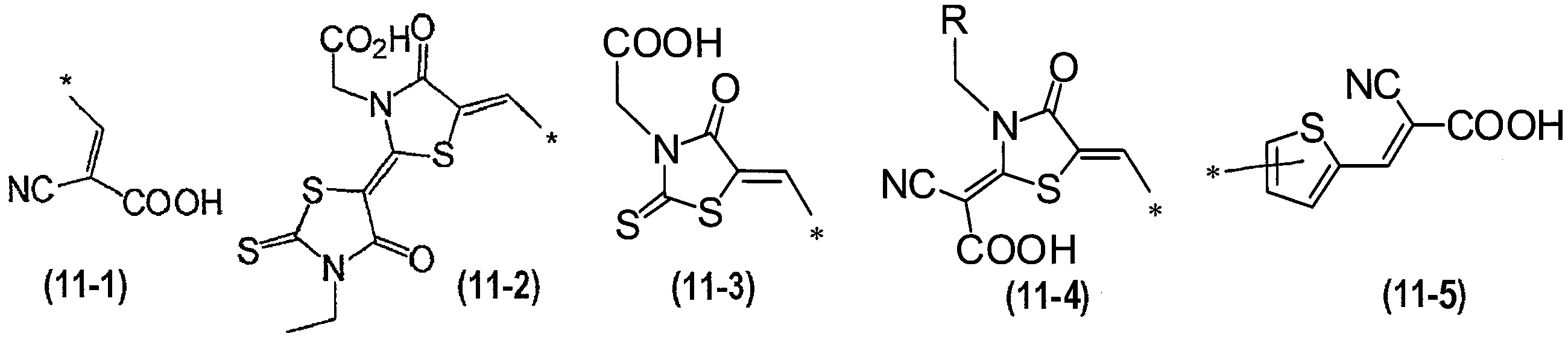
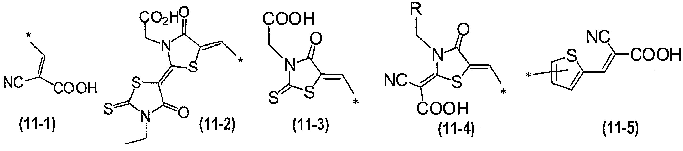
- A is represented by any of the following formulas (11-1) to (11-5):
- RaRbN—Ar— in the formula (1) or (2) is represented by any of the following formulas (12-1) to (12-5), and d and a are represented by the following formula (13-1) ) To (13-9)
- R 1 represents a hydrogen atom, an aliphatic group, an aromatic group or a heterocyclic group bonded with carbon.
- R 41 to R 50 represent a hydrogen atom or a substituent. * Represents a binding site.
- k1 represents an integer of 1 to 4, and k2 represents an integer of 1 to 3.
- R 51 to R 64 represent a hydrogen atom or a substituent.
- k3 represents an integer of 1 to 3. * Represents a binding site.
- a photoelectric conversion element comprising a conductive support, a photoreceptor layer having semiconductor fine particles and a sensitizing dye, a charge transfer layer having an electrolyte, and a counter electrode in the order, ⁇ 1> to ⁇ 8 A photoelectric conversion element using the dye described in any one of the above items as a sensitizing dye in the photoreceptor layer.
- a photoelectrochemical cell comprising the photoelectric conversion element according to ⁇ 9>.
- R′a to R′i represent a substituent.
- Na to nb represent an integer of 0 to 4.
- nc and ne represent an integer of 0 to 3.
- nd represents an integer of 0 to 2.
- nf, nj represents an integer of 0 to 4.
- an aromatic ring is used to mean an aromatic ring and a heterocyclic ring (aliphatic heterocyclic ring and aromatic heterocyclic ring).
- the carbon-carbon double bond may be either E-type or Z-type. What is necessary is just to interpret so that resonance structural formula may be materialized without inconsistency in the structural formula and connection of each site
- the respective substituents or ligands may be the same or different from each other. The same applies to the definition of the number of substituents and the like.
- a plurality of substituents, ligands, and linking groups are close to each other, they may be connected to each other or condensed to form a ring.
- the group having an acidic group includes an acidic nucleus.
- the present invention it is possible to provide a photoelectric conversion element and a photoelectrochemical cell having high conversion efficiency and excellent durability, and a dye used therefor.
- the present inventors have been able to effectively use light because a dye having a specific structure can absorb light of a long wavelength, and have high conversion efficiency and excellent durability. It has been found that a chemical battery can be provided. The present invention has been made based on this finding.
- the photoelectric conversion element 10 includes a conductive support 1, a photosensitive layer 2, a charge transfer layer 3, and a counter electrode 4 arranged in that order on the conductive support 1.
- the conductive support 1 and the photoreceptor layer 2 constitute a light receiving electrode 5.
- the photoreceptor layer 2 has semiconductor fine particles 22 and a sensitizing dye (hereinafter also simply referred to as a dye) 21. At least a part of the sensitizing dye 21 is adsorbed on the semiconductor fine particles 22 (the sensitizing dye 21 is in an adsorption equilibrium state and may be partially present in the charge transfer layer 3).
- the charge transfer body layer 3 functions as, for example, a hole transport layer that transports holes.
- the conductive support 1 on which the photoreceptor layer 2 is formed functions as a working electrode in the photoelectric conversion element 10.
- the photoelectric conversion element 10 can be operated as the photoelectrochemical cell system 100 by causing the external circuit 6 to work.
- the light receiving electrode 5 is an electrode composed of a conductive support 1 and a photosensitive layer 2 (semiconductor film) of semiconductor fine particles 22 adsorbed by a sensitizing dye 21 coated on the conductive support 1.
- a photosensitive layer 2 semiconductor film
- the excited dye has high energy electrons. Therefore, the electrons are transferred from the sensitizing dye 21 to the conduction band of the semiconductor fine particles 22 and reach the conductive support 1 by diffusion.
- the molecule of the sensitizing dye 21 is an oxidant.
- the electrons on the electrodes return to the oxidant while working in the external circuit 6 to operate as the photoelectrochemical cell system 100.
- the light receiving electrode 5 functions as a negative electrode of the battery.
- the photoreceptor layer 2 is composed of a porous semiconductor layer composed of a layer of semiconductor fine particles 22 to which a dye described later is adsorbed. This dye may be partially dissociated in the electrolyte.
- the photoreceptor layer 2 is designed according to the purpose and has a multilayer structure.
- the upper and lower sides of the photoelectric conversion element do not need to be defined in particular, but in this specification, based on what is illustrated, the side of the counter electrode 4 serving as the light receiving side is the upper (top) direction, and the support The side of 1 is the lower (bottom) direction.
- the light receiving electrode 5 may be defined as including a part of the charge transfer layer 3.
- the photosensitive layer 2 includes the semiconductor fine particles 22 on which the specific dye is adsorbed, the light receiving sensitivity is high, and when used as the photoelectric conversion element 10, high photoelectric conversion efficiency can be obtained. Furthermore, it has high durability.
- dye of this invention consists of a compound represented by following formula (1) or (2).
- A represents a group having an acidic group.
- Ar represents an aromatic ring.
- Ra and Rb represent a hydrogen atom, an aliphatic group, an aromatic group, or a heterocyclic group bonded with a carbon atom.
- n, L and m are integers of 1 to 5.
- d and a are the following specific linking groups. ]
- the dye of the present invention has a donor group (RaRbN—Ar) (hereinafter, this group may be referred to as part D) and a group having at least one acidic group or a group having an acidic nucleus at both terminals. And an acceptor site A.
- This donor site D and acceptor site A are each bonded to a linking group to constitute a dye comprising the compound represented by formula (1) or (2).
- This linking group is a donor linking group d and / or an acceptor linking group a.
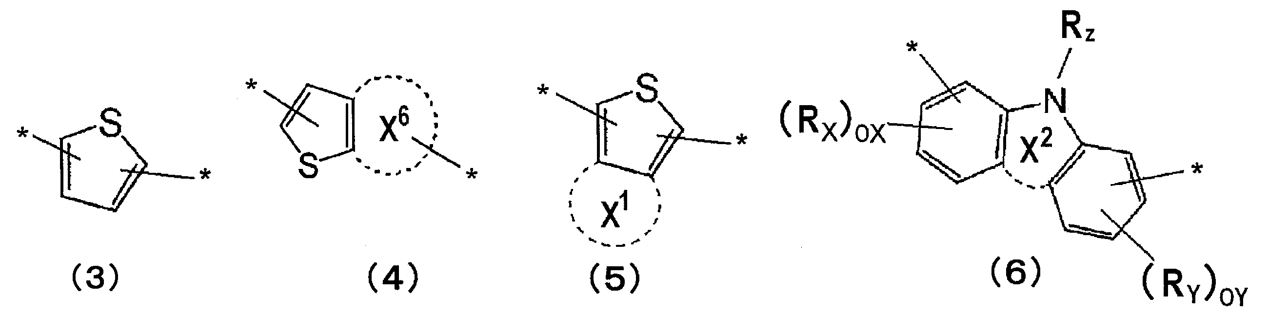
- the donor linking group d and the acceptor linking group a are represented by any of the following formulas (3) to (6).
- the linking group not only connects the donor site (D) and the acceptor site (A), but also has a donor linking group (d) and / or an acceptor linking group (a). Therefore, when the light is irradiated, electron movement can be performed strongly and quickly, and light having a long wavelength can be absorbed to improve the photoelectric conversion efficiency.
- the dye of the present invention has a D site in order to introduce a donor site having a wide conjugated system and stabilize the one-electron oxidation state of the dye.
- Ra and Rb are bonded to a nitrogen atom, and are further bonded to a linking group described later via Ar. With this structure, the conjugated system is widened, so that the effect of stabilizing the electronic oxidation state and the effect of increasing the absorption wavelength can be achieved.
- Ra and Rb are a hydrogen atom, an aliphatic group, an aromatic group, or a heterocyclic group bonded with a carbon atom.
- Examples of the aliphatic group for Ra and Rb include an alkyl group, an alkenyl group, and an alkynyl group.
- Examples of the aromatic group include a benzyl group, a naphthyl group, and an anthracene group.
- Examples of the heterocyclic group include a thiophene group and a pyrrole group. Of these, a benzyl group, a thiophene group and the like are preferable.
- Ra and Rb may be connected to each other to form a ring structure. Further, at least one of Ra and Rb may be bonded to or condensed with Ar to form a ring structure.
- part has couple
- aromatic ring a benzyl group, a naphthyl group, an anthracene group and the like are preferable, and a benzyl group is more preferable.
- heterocyclic ring a thiophene group, a pyrrole group and the like are preferable, and a thiophene group is more preferable. Since the D site is bonded to the linking group described later via the aromatic ring Ar, coupled with the structure of the linking group described later, the conjugated system is extended so that it absorbs light of a long wavelength, and one-electron oxidation. The effect which stabilizes a state can be show
- the D site is preferably represented by the following formula (7).
- X 3 represents an atomic group forming a nitrogen-containing heterocyclic ring. * Represents a binding site.
- R 1 represents a hydrogen atom, an aliphatic group, an aromatic group or a heterocyclic group bonded with carbon.
- the atomic group X 3 necessary for forming the benzene ring to be linked and the nitrogen-containing heterocyclic ring is an atomic group in which at least one selected from the group consisting of a carbon atom, an oxygen atom, a nitrogen atom and a sulfur atom is bonded.
- X 3 is preferably a 4- to 8-membered ring composed of a carbon atom in addition to a nitrogen atom. More preferred is a 5- to 7-membered ring.
- Examples of the 4-membered ring to 8-membered ring include a pyrrolidine ring, a piperidine ring, a hexamethyleneimine ring, an azacyclooctane ring, a morpholine ring, and a thiomorpholine ring. More preferred are a pyrrolidine ring, a hexamethyleneimine ring, and a thiomorpholine ring.
- R 1 represents a hydrogen atom, an aliphatic group, an aromatic group, or a heterocyclic group bonded with a carbon atom.
- R 1 include substituted or unsubstituted alkyl groups having 1 to 20 carbon atoms (for example, methyl, ethyl, n-butyl, n-hexyl, isobutyl, sec-butyl, t-butyl, n-dodecyl, Cyclohexyl, benzyl, etc.), substituted or unsubstituted aryl groups (eg, phenyl, tolyl, naphthyl, etc.), substituted or unsubstituted heterocyclic residues (eg, pyridyl, imidazolyl, furyl, thienyl, oxazolyl, thiazolyl, benzimidazolyl, quinolyl) More preferably, it is a substituted
- the D is preferably represented by the following formula (8).
- X 4 represents an atomic group necessary for forming a nitrogen-containing heterocyclic ring. * Represents a binding site with d.
- O1 and O2 independently represent an integer of 0 or more.
- Z 11 and Z 12 represent a substituent.
- R 1 represents a hydrogen atom, an aliphatic group, an aromatic group or a heterocyclic group bonded with carbon.
- the atomic group X 4 necessary for forming the benzene ring to be linked and the nitrogen-containing heterocyclic ring is at least one selected from the group consisting of a carbon atom, an oxygen atom, a nitrogen atom and a sulfur atom.
- a group of atoms with bonded species is preferred.
- X 4 is preferably a 4- to 8-membered ring composed of a carbon atom in addition to a nitrogen atom. More preferably, it is a 5-membered ring to a 7-membered ring.
- R 1 in Formula (8) can be the same as R 1 in Formula (7).
- Z 11 and Z 12 represent a substituent, and Z 11 and Z 12 may be the same or different.
- the substituent include an aliphatic group, an aromatic group, and a heterocyclic group.
- Specific examples of the substituent include alkyl groups, alkoxy groups, alkylthio groups, aryl groups, aryloxy groups, arylthio groups, and heterocyclic rings.
- Preferable examples include alkyl groups (eg, methyl, ethyl, n-butyl, n-hexyl, isobutyl, sec-butyl, t-butyl, n-dodecyl, cyclohexyl, benzyl, etc.), substituted aryl groups (eg, phenyl, tolyl, Naphthyl and the like) and alkoxy groups (for example, methoxy, ethoxy, isopropoxy, butoxy and the like).
- the number of substituents O1 and O2 independently represents an integer of 0 or more.
- the number of substituents is preferably 0 to 3, more preferably 0 to 1.
- the D is preferably represented by the following formula (9).
- X 5 represents an atomic group necessary for forming a nitrogen-containing heterocyclic ring.
- R 1 represents a hydrogen atom, an aliphatic group, an aromatic group or a heterocyclic group bonded with carbon.
- R 12 to R 18 represent a hydrogen atom or a substituent. * Represents a binding site. ]
- the atomic group X 5 forming the nitrogen-containing heterocycle to be linked is preferably an atomic group in which at least one selected from the group consisting of a carbon atom, an oxygen atom, a nitrogen atom and a sulfur atom is bonded.
- X 5 is preferably a 4- to 8-membered ring composed of a carbon atom in addition to a nitrogen atom. More preferably, it is a 5-membered ring to a 7-membered ring.
- R 1 may be the same as the formula (7).
- preferred substituents for R 12 to R 18 preferred are Z 11 and Z 12 in the formula (8).
- the D is preferably represented by any of the following formulas (12-1) to (12-5).
- R 1 represents a hydrogen atom, an aliphatic group, an aromatic group or a heterocyclic group bonded with carbon.
- R 41 to R 50 represent a hydrogen atom or a substituent. Examples of the substituent in R 41 to R 50 include the same substituents as Z 11 and Z 12 in formula (8). * Represents a binding site.
- k1 represents an integer of 1 to 4, and k2 represents an integer of 1 to 3.
- the acceptor site (A) is a group having at least one acidic group (including a group having an acidic nucleus).
- acidic nucleus T.I. H. "The Theory of the photographic process. Forth edition.” By James, published in 1977, published by Macmillan publishing, Inc.
- Preferred examples of the acidic nucleus include rhodanine nucleus, hindantin, thiohydantoin, barbituric acid, pyrazolidinedione, pyrazolone, and indandione. These may include those in which two or more acidic nuclei dehydrated and condensed at the carbonyl moiety are linked.
- Preferred are rhodanine, hindantin, thiohydantoin, barbituric acid, and pyrazolidinedione, and particularly preferred is rhodanine.
- An acidic group represents a proton dissociable group having a pKa of 13 or less.
- Preferable specific examples of the acidic group include carboxylic acid, sulfonic acid, phosphoric acid, phosphate ester and the like. More preferred examples of the acidic group include carboxylic acid.
- the carbon-carbon double bond may be either E-type or Z-type.
- the acidic group may be a salt of the acidic group.
- the acidic nucleus When the acidic nucleus has at least one acidic group, it preferably has an electron withdrawing group at the same time, and examples of the electron withdrawing group include substituents having the effects described below (-I effect and -M effect). It is done.
- the type and bonding position of the electron withdrawing group are appropriately selected so that the effect of increasing the overlap between the molecular orbital in the excited state of the dye and the light receiving electrode is exerted.
- an electron withdrawing group attenuates the electron density for a particular position in the molecule.
- the electron withdrawing property or electron donating property cannot be explained only by the difference in electronegativity.
- the induction effect and the mesomery effect act in a complex manner, and the appearance changes depending on the presence of aromaticity, conjugated system, and topological positional relationship.
- Hammett's rule is known as an empirical rule for quantitatively evaluating and predicting these effects based on the acid dissociation constants of para- and meta-substituted benzoic acids.
- the electron withdrawing property is represented as -I effect
- the electron donating property is represented as + I effect.
- An atom having a higher electronegativity than carbon exhibits an -I effect.
- An anion shows a + I effect
- a cation shows a -I effect.
- the A is preferably represented by any of the following formulas (11-1) to (11-5).
- * represents a binding site. Because of these groups, the adsorption power to oxide semiconductors (for example, titanium oxide) is high, and by conjugating with other sites in the molecule, it absorbs light having a long wavelength, and electrons are absorbed from within the molecule. An effect of facilitating transmission to an oxide semiconductor can be achieved.
- R represents a hydrogen atom or a substituent, and a substituent is preferable.
- substituent include the substituent T described later, and a preferred embodiment is the same as the substituent T.
- the linking group (d) and / or the linking group (a) having acceptor properties may be independent of each other (formula (2)).
- n, L, and m are integers of 1 to 5.
- R X and R Y represent a substituent.
- R Z represents a hydrogen atom, an aliphatic group, an aromatic group or a heterocyclic group bonded with carbon.
- X 6 and X 1 each represents an aromatic ring.
- X 2 represents a heterocyclic ring.
- OX and OY represent an integer of 0 to 3. * Represents a binding site.
- R X and R Y represent a substituent, and R X and R Y may be the same or different.
- the substituent include an aliphatic group, an aromatic group, and a heterocyclic group.
- Specific examples of the substituent include alkyl groups, alkoxy groups, alkylthio groups, aryl groups, aryloxy groups, arylthio groups, and heterocyclic rings.
- Preferable examples include alkyl groups (eg, methyl, ethyl, n-butyl, n-hexyl, isobutyl, sec-butyl, t-butyl, n-dodecyl, cyclohexyl, benzyl, etc.), substituted aryl groups (eg, phenyl, tolyl, Naphthyl and the like) and alkoxy groups (for example, methoxy, ethoxy, isopropoxy, butoxy and the like).
- R Z represents a hydrogen atom, an aliphatic group, or a heterocyclic group bonded with carbon.
- R Z includes the same as R 1 in the formula (7).
- examples of the aromatic ring include a benzene ring, a naphthalene ring, and an anthracene ring
- examples of the heterocyclic ring include a thiophene ring, a pyrrole ring, a thiazole ring, and an imidazole ring.
- a benzene ring, a naphthalene ring, a thiophene ring, etc. are preferable.
- the aromatic ring of X 6, a plurality of rings may be or a condensed ring or linked through an aliphatic ring.
- Examples of X 2 include a pyrrolidine ring, a piperidine ring, a hexamethyleneimine ring, an azacyclooctane ring, a morpholine ring, and a thiomorpholine ring. More preferred are a pyrrolidine ring, a hexamethyleneimine ring, and a thiomorpholine ring.
- Examples of the formula (4) include a linking group represented by the following formula (4 ′).
- R X and R Y are preferably bulky and hydrophobic, for example, an alkyl group (more preferably an alkyl group having 1 to 20 carbon atoms, particularly preferably an alkyl group having 1 to 15 carbon atoms), an alkenyl group (for example, propenyl).
- an alkyl group more preferably an alkyl group having 1 to 20 carbon atoms, particularly preferably an alkyl group having 1 to 15 carbon atoms
- an alkenyl group for example, propenyl
- alkynyl groups eg, propynyl, heptynyl, 2-ethylhexynyl, etc.
- ether groups eg, methoxy, heptoxy, 2-ethylhexoxy, etc.
- ester groups eg, methoxycarbonyl, heptoxy, etc.
- amino groups eg, methanamide, heptaneamide, 2-ethylhexamide, etc.
- More preferred are an alkyl group, an alkenyl group and an ether group.
- X 6 has the same meaning as X 6 above.
- the linking group is donor-type (d) or acceptor-type (a) is compared with the donor site (D) or acceptor site (A) bonded to both terminals, and the Winmostar calculation software
- Winmostar trade name, manufactured by Tencube Research Ltd.
- Winmostar trade name, manufactured by Tencube Research Ltd.
- the energy level of HOMO is calculated by molecular orbital calculation (Hamiltonian: AM1), and the same determination is made.
- the donor site (D) is 9-ethylcarbazole
- the acceptor site (A) is cyanoacetic acid
- the linking group a is thienothiophene
- the linking group d is benzodithiophene.
- other dyes can also determine a donor site (D), an acceptor site (A), and a linking group.
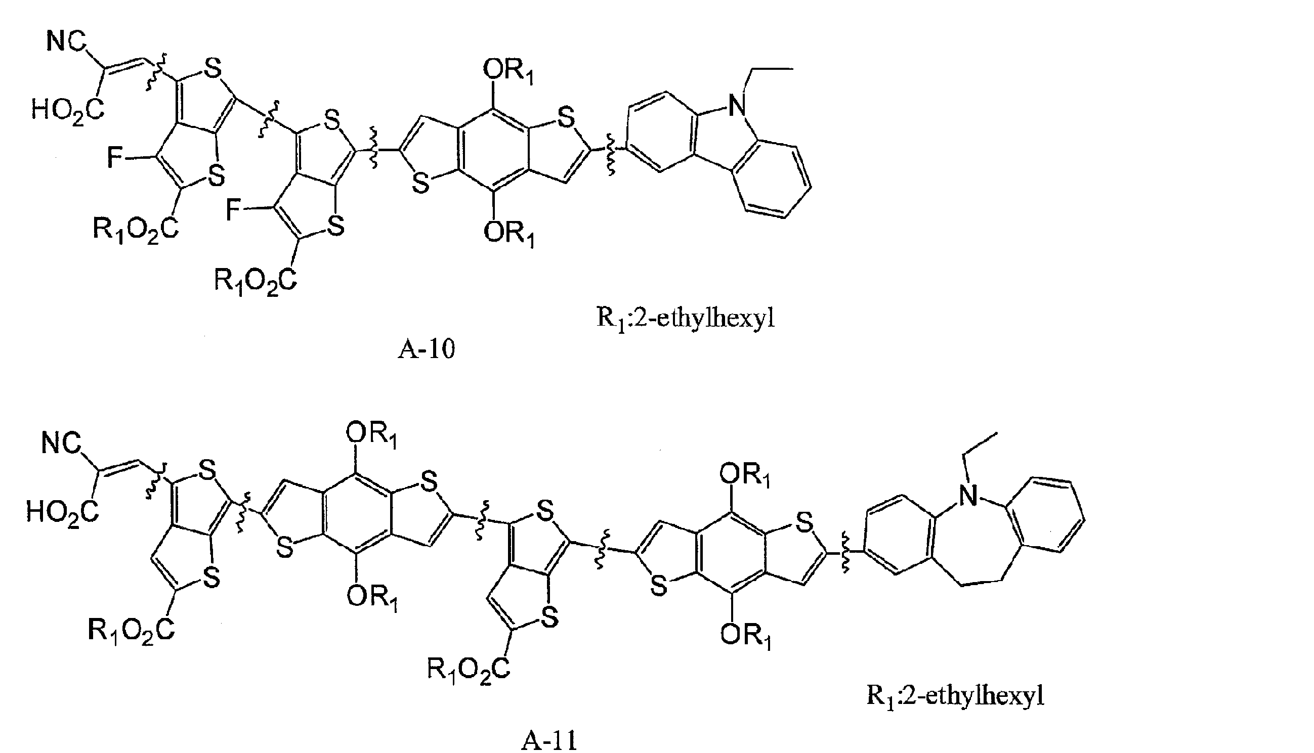
- A-2 to A-17 are also shown in the same manner. As shown below, each part and the donor and / or acceptor properties are sequentially shown from the left in the wavy line portion of each structural formula. Are linked to each other.
- A-1 A, a, d, D A-2: A, a, d, D A-3: A, a, d, D A-4: A, a, d, D A-5: A, a, d, D A-6: A, a, d, D A-7: A, a, d, d, d, D A-8: A, a, d, d, d, D A-9: A, a, a, d, d, d, D A-10: A, a, a, d, D A-11: A, a, d, a, d, D A-13: A, a, d, D A-14: A, a, d, D A-15: A, a, d, D A-16: A, a, d, D A-17: A, a, d, D
- Winmostar calculation software is software that performs molecular orbital calculation of a compound, and is provided as “Winnostar” (trade name) by Cube Research Institute.
- Winnostar trade name
- the energy level of the dye is within the range of the above condition (a)
- an effect of absorbing light having a longer wavelength than that of the conventional dye can be achieved.
- the donor linking group d and the acceptor linking group a it is preferable that the following condition (A) is further satisfied by molecular orbital calculation using Winmostar calculation software.
- (A) The difference in the HOMO energy rank between d and a is 0.01 to 1.0 eV.
- d can be a combination of (10-1), (10-5), and a can be a combination of (10-2).
- d is 13-6, 13-7, and a is 13-1 to 13-. 3, 13-9 combination.
- the LUMO of d and a is preferably ⁇ 2.0 to 0.1 eV, and more preferably ⁇ 1.5 to 0.1 eV.
- the HOMO of d and a is preferably ⁇ 9.5 to ⁇ 6.0 eV, and more preferably ⁇ 7.0 to ⁇ 9.0 eV.
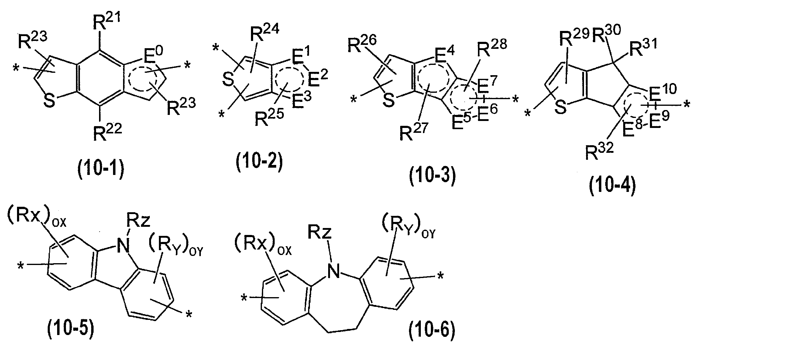
- the d and a are preferably represented by any of the following formulas (10-1) to (10-6).
- E 0 represents a nitrogen atom, an oxygen atom or a sulfur atom constituting a 5-membered heterocyclic ring.
- E 1 ⁇ E 3 represents a atom constituting the heterocyclic 5-membered ring, represents which at least one is a nitrogen atom, an oxygen atom or a sulfur atom, other represents CR W.
- R W represents a hydrogen atom or a substituent.
- E 4 represents an atom constituting a hetero 5-membered ring and represents a nitrogen atom, an oxygen atom or a sulfur atom.
- R X , R Y and R Z , OX, OY have the same meanings as in formula (6).
- R 21 to R 32 represent a hydrogen atom or a substituent. * Represents a binding site. ]
- the d and a are more preferably represented by any of the following formulas (13-1) to (13-9).
- R 51 to R 64 each represents a hydrogen atom or a substituent.
- substituent in R 51 to R 55 and R 64 include a linear or branched alkyl chain having 1 to 20 carbon atoms (eg, methyl, ethyl, 2-ethylhexyl, 3,3,5-trimethylhexyl ( Nonyl)) and the like. * Represents a binding site.
- the substituent in R 56 and R 57 is preferably a bulky and hydrophobic group.
- an alkyl group (more preferably an alkyl group having 1 to 20 carbon atoms, particularly preferably an alkyl group having 1 to 15 carbon atoms), an alkenyl group ( For example, propenyl, heptenyl, 2-ethylhexenyl etc.), alkynyl group (eg propynyl, heptynyl, 2-ethylhexynyl etc.), ether group (eg methoxy, heptoxy, 2-ethylhexoxy etc.), ester group (eg methoxycarbonyl , Heptoxycarbonyl, 2-ethylhexoxycarbonyl, etc.) and amino groups (eg, methanamide, heptanamide, 2-ethylhexamide, etc.). More preferred are an alkyl group, an alkenyl group, an ether (alkyloxy) group
- R 58 , R 59 , R 61 , and R 62 examples include an aliphatic group, an aromatic group, and a heterocyclic group. Specific examples of the substituent include alkyl groups, alkoxy groups, alkylthio groups, aryl groups, aryloxy groups, arylthio groups, and heterocyclic rings.
- Preferable examples include alkyl groups (eg, methyl, ethyl, n-butyl, n-hexyl, isobutyl, sec-butyl, t-butyl, n-dodecyl, cyclohexyl, benzyl, etc.), substituted aryl groups (eg, phenyl, tolyl, Naphthyl and the like) and alkoxy groups (for example, methoxy, ethoxy, isopropoxy, butoxy and the like).
- the number of substituents O1 and O2 independently represents an integer of 0 or more.
- the number of substituents is preferably 0 to 3, more preferably 0 to 1.
- R 60 and R 63 examples include a substituted or unsubstituted alkyl group having 1 to 20 carbon atoms (eg, methyl, ethyl, n-butyl, n-hexyl, isobutyl, sec-butyl, t-butyl, n- Dodecyl, cyclohexyl, benzyl, etc.), substituted or unsubstituted aryl groups (eg phenyl, tolyl, naphthyl, etc.), substituted or unsubstituted heterocyclic residues (eg pyridyl, imidazolyl, furyl, thienyl, oxazolyl, thiazolyl, benzimidazolyl) More preferably, a substituted or unsubstituted alkyl group having 1 to 20 carbon atoms (for example, methyl, ethyl, n-butyl, n-hexy
- the pigment of the present embodiment is preferably one represented by any of the following formulas (A1) to (A3).
- X 2 , Rx, and Ry have the same meaning as in formula (6).
- d, a, m, and L are synonymous with Formula (2).
- the dye represented by the formula (1) or (2) has a maximum absorption wavelength in the solution in the range of 550 to 750 nm, and more preferably in the range of 600 to 700 nm.
- the dye having the structure represented by the formula (1) or (2) used in the present invention is shown below, but the present invention is not limited thereto.
- dye in the following specific example contains the ligand which has a proton dissociable group, this ligand may dissociate as needed and may discharge
- a substituent for which substitution / non-substitution is not specified means that the group may have an arbitrary substituent. This is also synonymous for compounds that do not specify substitution / non-substitution.
- the ligand may be coordinated to the central metal as either an anionic ligand or a neutral ligand.
- Preferred substituents include the following substituent T.
- substituent T examples include the following.
- An alkyl group preferably an alkyl group having 1 to 20 carbon atoms, such as methyl, ethyl, isopropyl, t-butyl, pentyl, heptyl, 1-ethylpentyl, benzyl, 2-ethoxyethyl, 1-carboxymethyl, etc.
- alkenyl A group preferably an alkenyl group having 2 to 20 carbon atoms such as vinyl, allyl, oleyl and the like
- an alkynyl group preferably an alkynyl group having 2 to 20 carbon atoms such as ethynyl, butadiynyl, phenylethynyl and the like
- a cycloalkyl group preferably a cycloalkyl group having 3 to 20 carbon atoms, such as cyclopropyl, cyclopentyl, cyclohexyl, 4-methylcyclohex
- R 1 O 2 C— means an alkyloxycarbonyl group (R 1 —O— (C ⁇ O) —).
- the electrolyte composition used for the photoelectric conversion element 10 of the present invention includes, for example, a combination of iodine and iodide (for example, lithium iodide, tetrabutylammonium iodide, tetrapropylammonium iodide, etc.) as an oxidation-reduction pair, alkyl Combinations of viologens (for example, methyl viologen chloride, hexyl viologen bromide, benzyl viologen tetrafluoroborate) and reduced forms thereof, combinations of polyhydroxybenzenes (for example, hydroquinone, naphthohydroquinone, etc.) and oxidized forms thereof, bivalent and trivalent And combinations of divalent and trivalent cobalt complexes (eg, red blood salt and yellow blood salt).
- a combination of iodine and iodide, and a combination of divalent and trivalent cobalt eg, red blood
- Co (LL 2 ) m2 (X) m3 ⁇ CI Formula (14)
- LL 2 represents a bidentate or tridentate ligand represented by the following formula LL2.
- X represents a monodentate or bidentate ligand.
- M2 is an integer of 0 to 3.
- M3 represents an integer of 0 to 6.
- CI represents a counter ion when a counter ion is necessary to neutralize the charge.
- Za, Zb, and Zc represent an atomic group that can form a 5- or 6-membered ring. Za, Zb, and Zc may have a substituent, and (The ring may be closed. C represents 0 or 1.)
- X is preferably a halogen atom.
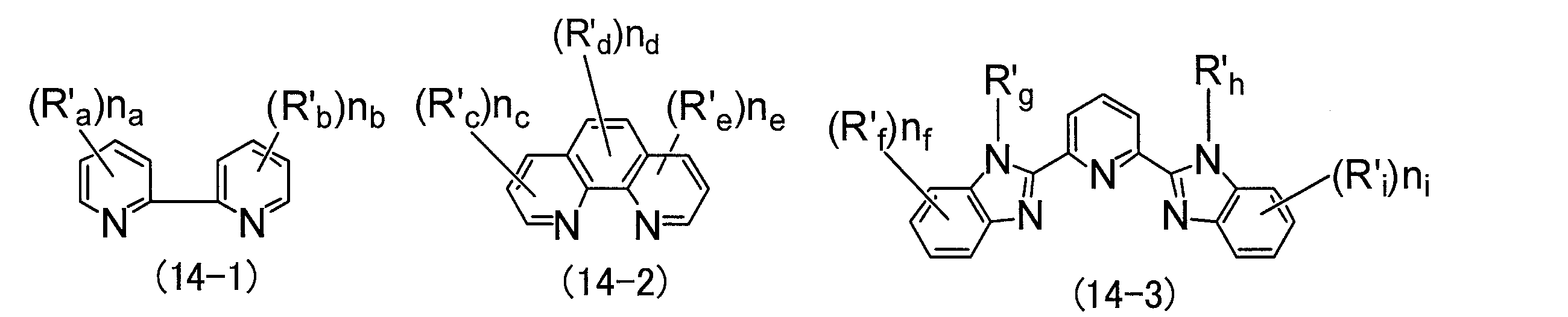
- LL2 in formula (14) is more preferably represented by the following formulas (14-1) to (14-3).
- R′a to R′i represent a substituent.
- Na to nb represent an integer of 0 to 4.
- nc and ne represent an integer of 0 to 3.
- nd represents an integer of 0 to 2.
- nf, nj represents an integer of 0 to 4.
- examples of the substituent for R′a to R′i include an aliphatic group, an aromatic group, and a heterocyclic group.
- Specific examples of the substituent include alkyl groups, alkoxy groups, alkylthio groups, aryl groups, aryloxy groups, arylthio groups, and heterocyclic rings.
- Preferable examples include alkyl groups (eg, methyl, ethyl, n-butyl, n-hexyl, isobutyl, sec-butyl, t-butyl, n-dodecyl, cyclohexyl, benzyl, etc.), substituted aryl groups (eg, phenyl, tolyl, Naphthyl and the like) and alkoxy groups (for example, methoxy, ethoxy, isopropoxy, butoxy and the like).
- the number of substituents O1 and O2 independently represents an integer of 0 or more.
- the number of substituents is preferably 0 to 3, more preferably 0 to 1.
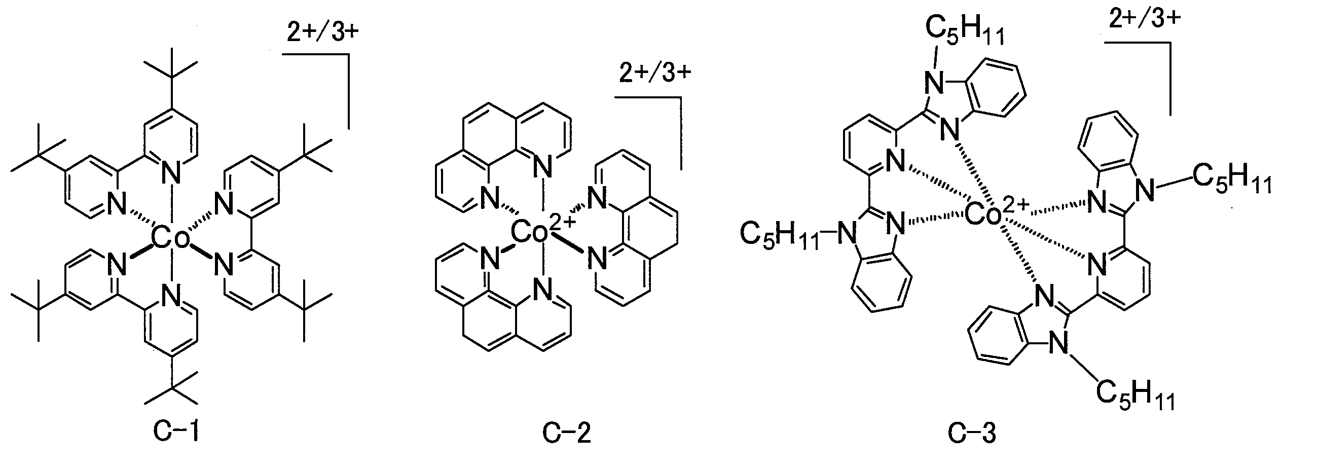
- cobalt complex examples include the following.
- the cation of the iodine salt is preferably a 5-membered or 6-membered nitrogen-containing aromatic cation.
- the compound represented by the formula (1) is not an iodine salt, republished WO95 / 18456, JP-A-8-259543, Electrochemistry, Vol. 65, No. 11, page 923 (1997). It is preferable to use iodine salts such as pyridinium salts, imidazolium salts and triazolium salts described in the above.
- the electrolyte composition used for the photoelectric conversion element 10 of the present invention preferably contains iodine together with a heterocyclic quaternary salt compound.
- the iodine content is preferably from 0.1 to 20% by mass, more preferably from 0.5 to 5% by mass, based on the entire electrolyte composition.
- the electrolyte composition used for the photoelectric conversion element 10 of the present invention may contain a solvent.
- the content of the solvent in the electrolyte composition is preferably 50% by mass or less, more preferably 30% by mass or less, and particularly preferably 10% by mass or less based on the entire composition.
- solvents those having a low viscosity and high ion mobility, a high dielectric constant and capable of increasing the effective carrier concentration, or both are preferable because they can exhibit excellent ion conductivity.
- solvents include carbonate compounds (ethylene carbonate, propylene carbonate, etc.), heterocyclic compounds (3-methyl-2-oxazolidinone, etc.), ether compounds (dioxane, diethyl ether, etc.), chain ethers (ethylene glycol dialkyl ether, Propylene glycol dialkyl ether, polyethylene glycol dialkyl ether, polypropylene glycol dialkyl ether, etc.), alcohols (methanol, ethanol, ethylene glycol monoalkyl ether, propylene glycol monoalkyl ether, polyethylene glycol monoalkyl ether, polypropylene glycol monoalkyl ether, etc.), Polyhydric alcohols (ethylene glycol, propylene glycol, polyethylene glycol , Propylene glycol, glycer
- an electrochemically inert salt that is in a liquid state at room temperature and has a melting point lower than room temperature may be used.
- an electrochemically inert salt that is in a liquid state at room temperature and has a melting point lower than room temperature
- 1-ethyl-3-methylimidazolium trifluoromethanesulfonate, 1-butyl-3-methylimidazolium trifluoromethanesulfonate, etc. nitrogen-containing heterocyclic quaternary salt compounds such as imidazolium salts and pyridinium salts, or tetraalkylammonium salts Is mentioned.
- the electrolyte composition used in the photoelectric conversion element of the present invention may be added with a polymer or an oil gelling agent, or may be gelled (solidified) by a technique such as polymerization of polyfunctional monomers or polymer crosslinking reaction. .
- the polyfunctional monomers are preferably compounds having two or more ethylenically unsaturated groups, such as divinylbenzene, ethylene glycol diacrylate, ethylene glycol dimethacrylate, diethylene glycol diacrylate, diethylene glycol dimethacrylate, triethylene glycol diacrylate, triethylene glycol Ethylene glycol dimethacrylate, pentaerythritol triacrylate, trimethylolpropane triacrylate and the like are preferable.
- divinylbenzene ethylene glycol diacrylate, ethylene glycol dimethacrylate, diethylene glycol diacrylate, diethylene glycol dimethacrylate, triethylene glycol diacrylate, triethylene glycol Ethylene glycol dimethacrylate, pentaerythritol triacrylate, trimethylolpropane triacrylate and the like are preferable.
- the gel electrolyte may be formed by polymerization of a mixture containing a monofunctional monomer in addition to the above polyfunctional monomers.
- Monofunctional monomers include acrylic acid or ⁇ -alkyl acrylic acid (acrylic acid, methacrylic acid, itaconic acid, etc.) or their esters or amides or vinyl esters (vinyl acetate, etc.), maleic acid or fumaric acid or their derivatives.
- Esters (dimethyl maleate, dibutyl maleate, diethyl fumarate, etc.), sodium salt of p-styrenesulfonic acid, acrylonitrile, methacrylonitrile, dienes (butadiene, cyclopentadiene, isoprene, etc.), aromatic vinyl compounds (Styrene, p-chlorostyrene, t-butylstyrene, ⁇ -methylstyrene, sodium styrenesulfonate, etc.), N-vinylformamide, N-vinyl-N-methylformamide, N-vinylacetamide, N-vinyl-N- Methylacetamide, Vinyl sulfonic acid, sodium vinyl sulfonate, sodium allyl sulfonate, sodium methacryl sulfonate, vinylidene fluoride, vinylidene chloride, vinyl alkyl ethers (such as methyl vinyl ether), ethylene,
- the blending amount of the polyfunctional monomer is preferably 0.5 to 70% by mass and more preferably 1.0 to 50% by mass with respect to the whole monomer.
- the above-mentioned monomers are the same as those described in Takayuki Otsu and Masaaki Kinoshita “Experimental Methods for Polymer Synthesis” (Chemistry Dojin) and Takayuki Otsu “Lecture Polymerization Reaction Theory 1 Radical Polymerization (I)” (Chemical Doujinshi). Polymerization can be performed by radical polymerization which is a polymer synthesis method.
- the monomer for gel electrolyte used in the present invention can be radically polymerized by heating, light or electron beam, or electrochemically, and is particularly preferably radically polymerized by heating.
- preferably used polymerization initiators are 2,2′-azobisisobutyronitrile, 2,2′-azobis (2,4-dimethylvaleronitrile), dimethyl 2,2′-azobis (2-methylpropyl). Pionate), azo initiators such as dimethyl 2,2′-azobisisobutyrate, peroxide initiators such as lauryl peroxide, benzoyl peroxide, and t-butyl peroctoate.
- a preferable addition amount of the polymerization initiator is 0.01 to 20% by mass, and more preferably 0.1 to 10% by mass with respect to the total amount of monomers.
- the weight composition range of the monomer in the gel electrolyte is preferably 0.5 to 70% by mass. More preferably, the content is 1.0 to 50% by mass.
- a polymer having a crosslinkable reactive group and a crosslinking agent is added to the composition.
- Preferred reactive groups are nitrogen-containing heterocycles such as pyridine ring, imidazole ring, thiazole ring, oxazole ring, triazole ring, morpholine ring, piperidine ring, piperazine ring, and the preferred crosslinking agent is a functional group capable of nucleophilic attack by the nitrogen atom.
- a photosensitive layer 2 in which a sensitizing dye 21 is adsorbed on porous semiconductor fine particles 22 is formed on a conductive support 1.
- the photoreceptor layer 2 can be produced by immersing the dispersion of semiconductor fine particles in the dye solution of the present invention after coating and drying on a conductive support.
- the conductive support 1 glass or a polymer material having a conductive film on the surface can be used as the support itself, such as metal.
- the conductive support 1 is preferably substantially transparent. Substantially transparent means that the light transmittance is 10% or more, preferably 50% or more, particularly preferably 80% or more.
- a glass or polymer material coated with a conductive metal oxide can be used as the conductive support 1, a glass or polymer material coated with a conductive metal oxide can be used. The coating amount of the conductive metal oxide at this time is preferably 0.1 to 100 g per 1 m 2 of glass or polymer material support. When a transparent conductive support is used, light is preferably incident from the support side.
- polymer materials examples include tetraacetyl cellulose (TAC), polyethylene terephthalate (PET), polyethylene naphthalate (PEN), syndiotactic polystyrene (SPS), polyphenylene sulfide (PPS), polycarbonate (PC), Examples include polyarylate (PAR), polysulfone (PSF), polyester sulfone (PES), polyetherimide (PEI), cyclic polyolefin, and brominated phenoxy.
- a surface may be provided with a light management function. For example, an antireflection film in which high refractive films and low refractive index oxide films described in JP-A-2003-123859 are alternately laminated, The light guide function described in JP-A-2002-260746 is improved.
- a metal support can also be preferably used.
- examples thereof include titanium, aluminum, copper, nickel, iron, stainless steel, and copper. These metals may be alloys. More preferably, titanium, aluminum, and copper are preferable, and titanium and aluminum are particularly preferable.
- the conductive support 1 has a function of blocking ultraviolet light.
- a method in which a fluorescent material capable of changing ultraviolet light into visible light is present in the transparent support or on the surface of the transparent support, or a method using an ultraviolet absorber is also included.
- JP-A-11-250944 may be further provided on the conductive support 1.
- Preferred conductive films include metals (eg, platinum, gold, silver, copper, aluminum, rhodium, indium, etc.), carbon, or conductive metal oxides (indium-tin composite oxide, tin oxide doped with fluorine, etc.) ).
- the thickness of the conductive film is preferably from 0.01 to 30 ⁇ m, more preferably from 0.03 to 25 ⁇ m, particularly preferably from 0.05 to 20 ⁇ m.
- the conductive support 1 preferably has a lower surface resistance.
- the range of the surface resistance is preferably 50 ⁇ / cm 2 or less, more preferably 10 ⁇ / cm 2 or less. Although there is no restriction
- a collecting electrode may be disposed.
- One or both of a gas barrier film and an ion diffusion preventing film may be disposed between the conductive support 1 and the transparent conductive film.
- a resin film or an inorganic film can be used as the gas barrier layer.
- a transparent electrode and a porous semiconductor electrode photocatalyst containing layer may be provided.
- the transparent conductive film may have a laminated structure, and as a preferable method, for example, FTO can be laminated on ITO.
- a photosensitive layer 2 in which a sensitizing dye 21 is adsorbed on porous semiconductor fine particles 22 is formed on a conductive support 1.
- the photoreceptor layer 2 can be produced by immersing the dispersion of the semiconductor fine particles 22 on the conductive support 1 and then immersing it in the above dye solution.
- the semiconductor fine particles 22 are preferably metal chalcogenides (for example, oxides, sulfides, selenides, etc.) or perovskite fine particles.
- metal chalcogenides for example, oxides, sulfides, selenides, etc.
- perovskite fine particles Preferred examples of the metal chalcogenide include titanium, tin, zinc, tungsten, zirconium, hafnium, strontium, indium, cerium, yttrium, lanthanum, vanadium, niobium, tantalum oxide, cadmium sulfide, cadmium selenide, and the like.
- Preferred perovskites include strontium titanate and calcium titanate. Of these, titanium oxide, zinc oxide, tin oxide, and tungsten oxide are particularly preferable.
- n-type semiconductors there are an n-type in which carriers involved in conduction are electrons and a p-type in which carriers are holes.
- n-type is preferable in terms of conversion efficiency.
- intrinsic semiconductors for example, intrinsic semiconductors
- the electron carrier concentration is reduced by structural defects derived from impurities.
- high n-type semiconductors there are high n-type semiconductors.
- the n-type inorganic semiconductor preferably used in the present invention is TiO 2 , TiSrO 3 , ZnO, Nb 2 O 3 , SnO 2 , WO 3 , Si, CdS, CdSe, V 2 O 5 , ZnS, ZnSe, SnSe, KTaO. 3 , FeS 2 , PbS, InP, GaAs, CuInS 2 , CuInSe 2 and the like.
- the most preferred n-type semiconductors are TiO 2 , ZnO, SnO 2 , WO 3 , and Nb 2 O 3 .
- a semiconductor material in which a plurality of these semiconductors are combined is also preferably used.
- the gel-sol method described in Sakuo Sakuo's “Science of Sol-Gel Method”, Agne Jofusha (1998), etc. is preferable. Also preferred is a method of producing an oxide by high-temperature hydrolysis of chloride developed by Degussa in an oxyhydrogen salt.
- the semiconductor fine particles 22 are titanium oxide
- the sol-gel method, the gel-sol method, and the high-temperature hydrolysis method in oxyhydrogen salt of chloride are all preferable. It is also possible to use the sulfuric acid method and the chlorine method described in Gihodo Publishing (1997).
- the sol-gel method the method described in Journal of American Ceramic Society, Vol. 80, No. 12, 3157-3171 (1997), or the chemistry of Burnside et al. The method described in Materials, Vol. 10, No. 9, pages 2419-2425 is also preferable.
- the semiconductor fine particle dispersion having a solid content other than the semiconductor fine particles of 10% by mass or less of the whole of the semiconductor fine particle dispersion is applied to the conductive support 1 and heated appropriately. Quality semiconductor fine particle coating layer can be obtained.
- a method of preparing a semiconductor fine particle dispersion is a method of depositing fine particles in a solvent and using them as they are when synthesizing a semiconductor. Ultrafine particles are irradiated with ultrasonic waves. Or a method of mechanically pulverizing and grinding using a mill or a mortar.
- the dispersion solvent one or more of water and various organic solvents can be used. Examples of the organic solvent include alcohols such as methanol, ethanol, isopropyl alcohol, citronellol and terpineol, ketones such as acetone, esters such as ethyl acetate, dichloromethane, acetonitrile and the like.
- a polymer such as polyethylene glycol, hydroxyethyl cellulose, carboxymethyl cellulose, a surfactant, an acid, or a chelating agent may be used in a small amount as a dispersion aid.
- these dispersing aids are preferably removed by a filtration method, a method using a separation membrane, a centrifugal method or the like before the step of forming a film on a conductive support.
- the solid content other than the semiconductor fine particles can be 10% by mass or less of the total dispersion. This concentration is preferably 5% or less, more preferably 3% or less, and particularly preferably 1% or less.
- the solid content other than the solvent and the semiconductor fine particles can be 10% by mass or less of the entire semiconductor fine dispersion. It is preferable to consist essentially of semiconductor fine particles and a dispersion solvent.
- the viscosity of the dispersion is preferably 10 to 300 N ⁇ s / m 2 at 25 ° C. More preferably, it is 50 to 200 N ⁇ s / m 2 at 25 ° C.
- a roller method, a dip method, or the like can be used as an application method.
- an air knife method, a blade method, etc. can be used as a metering method.
- the application method and the metering method can be made the same part.
- the wire bar method disclosed in Japanese Patent Publication No. 58-4589, the slide hopper method described in US Pat. No. 2,681,294, etc., the extrusion The method and the curtain method are preferable. It is also preferable to apply by a spin method or a spray method using a general-purpose machine.
- the wet printing method intaglio, rubber plate, screen printing and the like are preferred, including the three major printing methods of letterpress, offset and gravure. From these, a preferred film forming method is selected according to the liquid viscosity and the wet thickness. Further, since the semiconductor fine particle dispersion of the present invention has a high viscosity and has a viscous property, it may have a strong cohesive force and may not be well adapted to the support during coating. In such a case, by performing cleaning and hydrophilization of the surface by UV ozone treatment, the binding force between the applied semiconductor fine particle dispersion and the surface of the conductive support 1 is increased, and it becomes easy to apply the semiconductor fine particle dispersion. .
- the preferred thickness of the entire semiconductor fine particle layer is 0.1 ⁇ m to 100 ⁇ m.
- the thickness of the semiconductor fine particle layer is further preferably 1 ⁇ m to 30 ⁇ m, and more preferably 2 ⁇ m to 25 ⁇ m.
- the amount of the semiconductor fine particles supported per 1 m 2 of the support is preferably 0.5 g to 400 g, more preferably 5 g to 100 g.
- the amount of the dye of the present invention is preferably 5 mol% or more.
- the adsorption amount of the dye to the semiconductor fine particles is preferably 0.001 to 1 mmol, more preferably 0.1 to 0.5 mmol, with respect to 1 g of the semiconductor fine particles.
- the dye is a salt
- the counter ion of the specific metal complex dye is not particularly limited, and examples thereof include alkali metal ions and quaternary ammonium ions.
- the film forming method may be any one of (1) a wet method, (2) a dry method, and (3) an electrophoresis method (including an electrodeposition method), preferably (1) a wet method, or ( 2) A dry method, more preferably (1) a wet method.
- the coating amount of the semiconductor fine particles 22 per 1 m 2 of the support is preferably 0.5 g to 500 g, more preferably 5 g to 100 g.
- the counter electrode 4 functions as a positive electrode of the photoelectrochemical cell.
- the counter electrode 4 is generally synonymous with the conductive support 1 described above, but a support for the counter electrode is not necessarily required in a configuration in which the strength is sufficiently maintained. However, having a support is advantageous in terms of hermeticity.
- the material of the counter electrode 4 include platinum, carbon, and conductive polymer. Preferable examples include platinum, carbon, and conductive polymer.
- the structure of the counter electrode 4 is preferably a structure having a high current collecting effect.
- Preferred examples include JP-A-10-505192.
- the light receiving electrode 5 may be a composite electrode such as titanium oxide and tin oxide (TiO 2 / SnO 2 ).
- a mixed electrode of titania include Japanese Patent Application Laid-Open No. 2000-1113913.
- Examples of mixed electrodes other than titania include Japanese Patent Application Laid-Open Nos. 2001-185243 and 2003-282164.
- the photoelectric conversion element may have a structure in which a first electrode layer, a first photoelectric conversion layer, a conductive layer, a second photoelectric conversion layer, and a second electrode layer are sequentially stacked.
- the dyes used for the first photoelectric conversion layer and the second photoelectric conversion layer may be the same or different, and if they are different, it is preferable that the absorption spectra are different.
- the light receiving electrode 5 may be a tandem type in order to increase the utilization rate of incident light.
- Examples of preferred tandem type configurations include those described in JP-A Nos. 2000-90989 and 2002-90989.
- a light management function for efficiently performing light scattering and reflection inside the layer of the light receiving electrode 5 may be provided.
- Preferable examples include those described in JP-A-2002-93476.
- a short-circuit prevention layer between the conductive support 1 and the porous semiconductor fine particle layer in order to prevent reverse current due to direct contact between the electrolyte and the electrode.
- Preferable examples include Japanese Patent Application Laid-Open No. 06-507999.
- a spacer or a separator In order to prevent contact between the light receiving electrode 5 and the counter electrode 4, it is preferable to use a spacer or a separator.
- a preferable example is JP-A-2001-283941.
- Cell and module sealing methods include polyisobutylene thermosetting resin, novolak resin, photo-curing (meth) acrylate resin, epoxy resin, ionomer resin, glass frit, method using aluminum alkoxide for alumina, low melting point glass paste It is preferable to use a laser melting method. When glass frit is used, powder glass mixed with acrylic resin as a binder may be used.
- a transparent conductive film was produced by forming an FTO film on a glass substrate. Then, a transparent electrode plate was obtained by forming a semiconductor fine particle layer on the transparent conductive film. And the photoelectrochemical cell was produced using the transparent electrode plate, and conversion efficiency was measured.
- the method is as follows (1) to (3). (1) Preparation of FTO (fluorine-doped tin oxide) membrane raw material compound solution 0.701 g of tin (IV) chloride pentahydrate was dissolved in 10 mL of ethanol, and 0.592 g of a saturated aqueous solution of ammonium fluoride was added thereto.
- FTO fluorine-doped tin oxide
- a photoelectrochemical cell having a structure shown in FIG. 2 of Japanese Patent No. 4260494 was produced using a transparent electrode plate.
- the oxide semiconductor porous film is formed by dispersing titanium oxide fine particles having an average particle diameter of about 7 nm in acetonitrile to form a paste, which is applied onto the transparent electrode 11 by a bar coating method, dried, and baked at 450 ° C. for 1 hour. I went there. Thereafter, an acetonitrile paste liquid of titanium oxide fine particles having an average particle diameter of about 400 nm is further applied, and this is applied onto the transparent electrode 11 by a bar coating method, dried and baked at 450 ° C. for 1 hour, and has a thickness of 15 ⁇ m. A semiconductor fine particle layer having a thickness of 5 mm was formed.
- the dyes listed in Table 1 were dissolved in absolute ethanol at a concentration of 3 ⁇ 10 ⁇ 4 mol / liter to prepare an adsorption dye solution.
- dye here has shown as a specific example previously.
- the transparent substrate having the obtained titanium oxide film and the transparent conductive film is placed in a container in this adsorption dye solution, and the dye is adsorbed by infiltrating for about 4 hours to obtain a light receiving electrode. It was. Thereafter, it was washed several times with absolute ethanol and dried at about 60 ° C. for about 20 minutes.
- an electrolytic solution was prepared by dissolving lithium iodide at a concentration of 0.5 mol / liter and iodine at a concentration of 0.05 mol / liter using PC as a solvent.
- the above-mentioned light receiving electrode was immersed in this solution for about 2 hours, so that the redox electrolyte was infiltrated.
- a conductive substrate equipped with a platinum film is installed, the periphery is sealed with an epoxy-based sealant, and a redox electrolyte is injected as is between the counter electrode and sealed to produce a photoelectric conversion element. Produced.
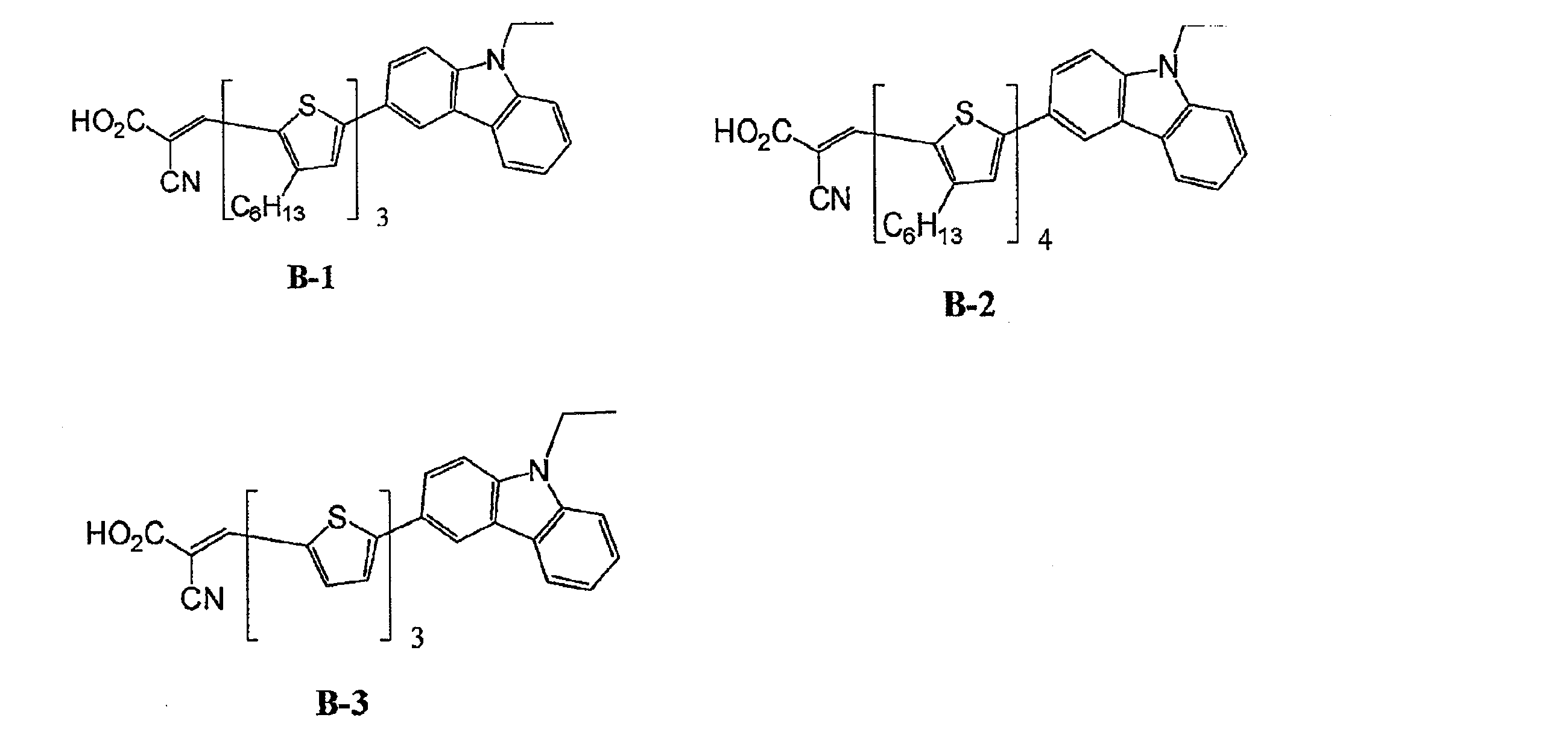
- the comparative dye B-1 was cut at the wavy line portion of each structural formula, and the difference between the energy level of each portion and the HOMO energy levels of the d portion and the a portion was obtained. These values were similarly calculated for B-2 and B-3.
- the dye of the present invention has a high maximum absorption wavelength, and is excellent in the initial value and durability of photoelectric conversion efficiency.
- Tests 201 to 204 and C21 to C24 shown below were performed in the same manner as Tests 101 to 110 except that the dyes in the table were used and the electrolyte was changed from iodine to the one described in the table.
Landscapes
- Chemical & Material Sciences (AREA)
- Organic Chemistry (AREA)
- Engineering & Computer Science (AREA)
- Materials Engineering (AREA)
- Power Engineering (AREA)
- Physics & Mathematics (AREA)
- Spectroscopy & Molecular Physics (AREA)
- Microelectronics & Electronic Packaging (AREA)
- Hybrid Cells (AREA)
- Nitrogen And Oxygen Or Sulfur-Condensed Heterocyclic Ring Systems (AREA)
- Photovoltaic Devices (AREA)
- Nitrogen Condensed Heterocyclic Rings (AREA)
Abstract
Description
本発明の課題は、長波長の光を十分利用できるため初期の光電変換効率が高く、しかも耐久性に優れた光電変換素子及び光電気化学電池、並びにそれに用いられる色素を提供することにある。
<1>下記式(1)又は(2)で表される化合物よりなる色素。


<2>前記色素のd及びaが、Winmostar計算ソフトによる分子軌道計算でLUMOが-3.0~0eV、HOMOが-9.5~-6.0eVである<1>記載の色素。
<3>前記式(1)及び(2)において、前記dとaのうち、Winmostar計算ソフトによる分子軌道計算でHOMOのエネルギー順位の高い基をd、他方をaとし、HOMOのエネルギー順位の差は0.01~1.0eVである<1>又は<2>記載の色素。
<4>前記式(1)又は(2)のRaRbN-Ar-が下記式(7)で表される<1>~<3>のいずれか1項記載の色素。

<5>前記式(1)又は(2)のRaRbN-Ar-が下記式(8)で表される<1>~<4>のいずれか1項記載の色素。

<6>前記式(1)又は(2)のRaRbN-Ar-が下記式(9)で表され、前記d及びaが下記式(10-1)~(10-6)のいずれかで表される<1>~<5>のいずれか1項記載の色素。

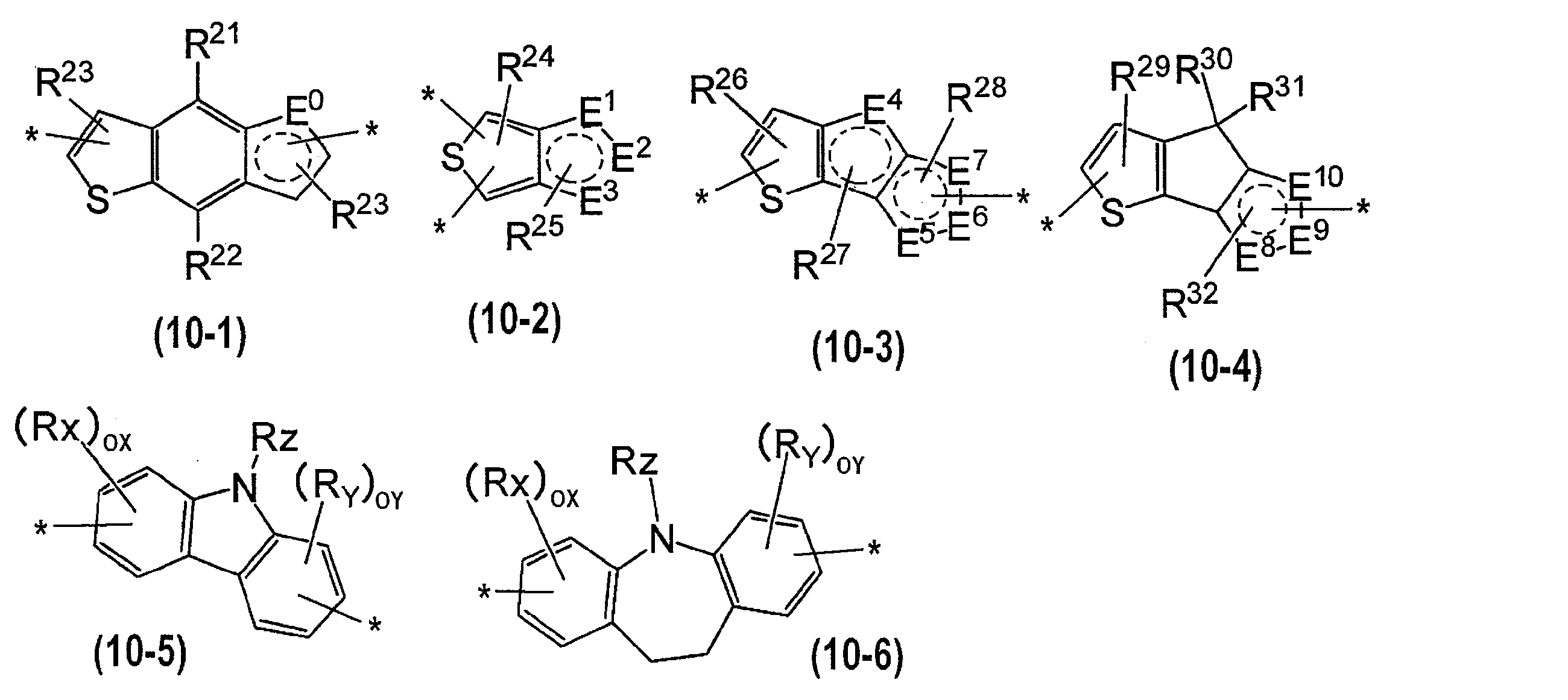
<7>前記Aが下記式(11-1)~(11-5)のいずれかで表される<1>~<6>のいずれか1項記載の色素。
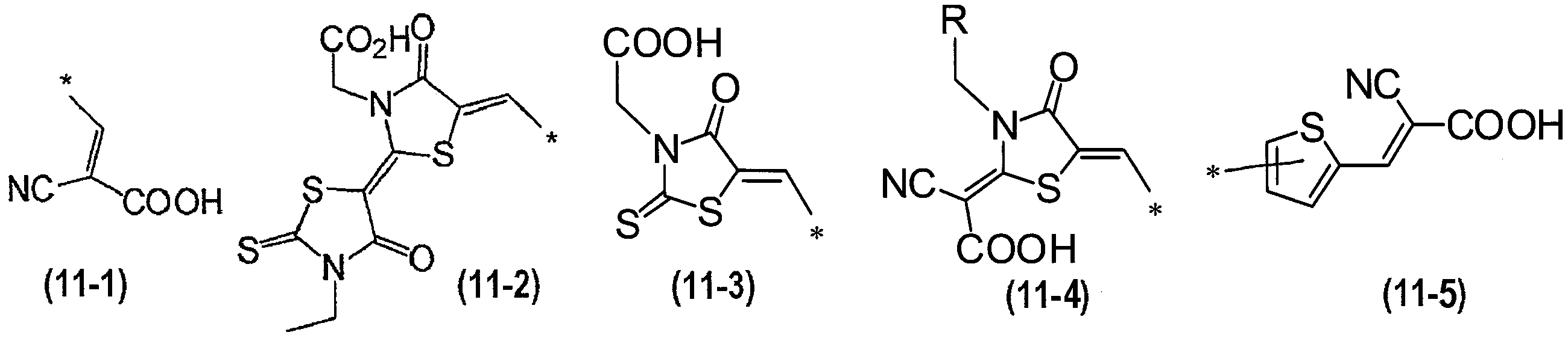
<8>前記式(1)又は、(2)のRaRbN-Ar-が下記式(12-1)~(12-5)のいずれかで表され、前記d及びaが下記式(13-1)~(13-9)のいずれかで表される<1>~<7>のいずれか1項記載の色素。

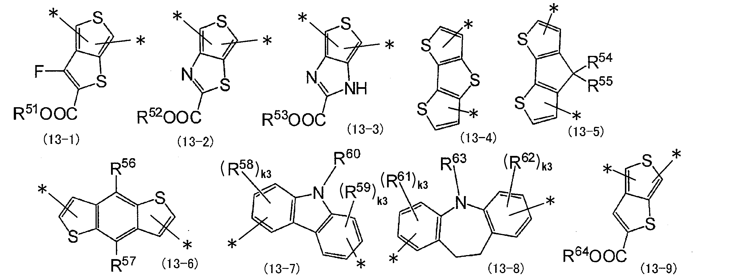
<9>導電性支持体、半導体微粒子と増感色素とを有する感光体層、電解質を有する電荷移動体層、及び対極をその順序で具備する光電変換素子であって、<1>~<8>のいずれか1項記載の色素を前記感光体層中の増感色素として用いる光電変換素子。
<10><9>に記載の光電変換素子を備える光電気化学電池。
<11>前記電荷移動体層中の電解質がコバルト錯体である<9>に記載の光電変換素子。
<12>前記コバルト錯体が式(14)で表される<11>に記載の光電変換素子。
Co(LL2)m2(X)m3・CI : 式(14)
[式(14)において、LL2は下記式LL2で表される2座又は3座の配位子を表す。Xは1座又は2座の配位子を表す。m2は0~3の整数を表す。m3は0~6の整数を表す。CIは電荷を中和させるのに対イオンが必要な場合の対イオンを表す。]

<13>Xがハロゲン原子であることを特徴とした<11>又は<12>記載の光電気変換素子。
<14>式(14)中のLL2が下記式(14-1)~(14-3)で表される<11>~<13>のいずれかに記載の光電変換素子。

なお、光電変換素子の上下は特に定めなくてもよいが、本明細書において、図示したものに基づいて言えば、受光側となる対極4の側を上部(天部)の方向とし、支持体1の側を下部(底部)の方向とする。なお、受光電極5は電荷移動体層3の一部を含むものとして定義してもよい。
本発明の色素は、下記式(1)又は(2)で表される化合物よりなる。

本発明の色素は、式(1)及び(2)において、共役系の広がったドナー部位を導入して、色素の一電子酸化状態を安定化させるために、D部位を有している。D部位は、窒素原子にRa及びRbが結合し、さらにArを介して後述の連結基と結合している。この構造により、共役系が広がることで、電子酸化状態を安定化する効果と、吸収する波長が長波長化する効果を奏することができる。Ra、Rbは、水素原子、脂肪族基、芳香族基又は炭素原子で結合する複素環基である。Ra、Rbの脂肪族基としては、アルキル基、アルケニル基、アルキニル基などを挙げることができる。芳香族基としては、ベンジル基、ナフチル基、アントラセン基などを挙げることができる。複素環基としては、チオフェン基、ピロール基などを挙げることができる。このうち、ベンジル基、チオフェン基などが好ましい。Ra、Rbは互いに連結して環構造を形成していてもよい。また、Ra、Rbの少なくともいずれかがArと結合ないし縮合して環構造を形成していてもよい。
D部位は、芳香環のArを介して後述の連結基と結合している。芳香族環としては、ベンジル基、ナフチル基、アントラセン基などが好ましく、さらに好ましくは、ベンジル基である。複素環としては、チオフェン基、ピロール基などが好ましく、さらに好ましくは、チオフェン基である。D部位が芳香環のArを介して後述の連結基と結合していることにより、後述の連結基の構造とあいまって、共役系が伸びるため長波長の光を吸収し、また、一電子酸化状態を安定化する効果を奏することができる。


[式(8)において、X4は含窒素複素環を形成するのに必要な原子群を表す。*はdとの結合部位を表す。O1及びO2は、独立に0以上の整数を表す。Z11及びZ12は置換基を表す。R1は水素原子、脂肪族基、芳香族基又は炭素で結合する複素環基を表す。]
置換基の数O1及びO2は、独立に0以上の整数を表す。置換基の数は好ましくは0~3、さらに好ましくは0~1である。


*は結合部位を表す。
k1は1~4の整数を表し、k2は1~3の整数を表す。
アクセプター性の部位(A)は、酸性基を少なくとも1つ有する基(酸性核を有する基を含む)である。酸性核(A)としては、T.H.James著「The Theory of the photografic process. forth edition.」Macmillan publishing社,1977年刊の199ページに記載のものが挙げられる。
一般に、電子求引基は分子の特定の位置について電子密度を減弱させる。電子求引性あるいは電子供与性は単に電気陰性度の差だけでは説明できない。すなわち、誘起効果やメソメリー効果などが複合的に作用するので、芳香性や共役系の存在やトポロジー的な位置関係によって現れ方が変わってくる。これらの効果を、パラ及びメタ置換安息香酸の酸解離定数をもとに定量的に評価、予測する経験則としてハメット則が知られている。誘起効果の場合、電子求引性のものを-I効果、電子供与性のものを+I効果と表すが、炭素よりも電気陰性度の高い原子は-I効果を示す。また、アニオンは+I効果を、カチオンは-I効果を示す。メソメリー効果の場合は、電子求引性のものを-M効果、電子供与性のものを+M効果と表す。電子求引基の例を以下に示す。
誘起効果
(-I効果)
・-O+R2 > -N+R3
・-N+R3 > -P+R3 > …
・-O+R2 > -S+R2 > …
・-N+R3 > -NO2 > -SO2R > -SOR
・-SO2R > -SO3R
・-N+R3 > -NR2
・-O+R2 > -OR
・-S+R2 > -SR
・-F > -Cl > -Br > -I
・=O > =NR > =CR2
・=O > -OR
・≡N > ≡CR
・≡N > =NR > -NR2
・-C≡CR > -CR=CR2 > -CR2CR3
メソメリー効果
(-M効果)
・=N+R2 > =NR
・=O > =NR > =CR2
・=S > =O > ≡N
連結基は、ドナー性を有する連結基(d)とアクセプター性を有する連結基(a)との組合せが単数又は複数からなるもの(式(1))でも、ドナー性を有する連結基(d)及び/又はアクセプター性を有する連結基(a)とがそれぞれ独立してなるもの(式(2))でもよい。式(1)及び(2)において、n、L、mは1~5の整数である。

RZとしては、水素原子、脂肪族基又は炭素で結合する複素環基を表す。好ましいRZとしては、前記式(7)におけるR1と同様のものを挙げることができる。

X6は先のX6と同義である。
後述のその他の具体例である、A-2~A-17についても、同様に示すと、以下のとおり、各構造式の波線部分で、左から順に、各部位とドナー性及び/又はアクセプター性の連結基が結合している。
A-1:A,a、d、D
A-2:A、a、d、D
A-3:A、a、d、D
A-4:A、a、d、D
A-5:A、a、d、D
A-6:A、a、d、D
A-7:A、a、d、d、d、D
A-8:A、a、d、d、d、D
A-9:A、a、a、d、d、d、D
A-10:A、a、a、d、D
A-11:A、a、d、a、d、D
A-13:A、a、d、D
A-14:A、a、d、D
A-15:A、a、d、D
A-16:A、a、d、D
A-17:A、a、d、D
(ア)色素のd及びaのLUMOが-3.0~0eVで、かつHOMOが-9.5~-6.0eVである。
色素のエネルギー準位が上記の条件(ア)の範囲内であることにより、従来の色素よりも長波長の光を吸収する効果を奏することができる。また、dおよびaにエネルギー勾配を形成するという点から、以下の条件(イ)を満たすことが好ましい。
(イ)dとaのHOMOのエネルギー順位の差は0.01~1.0eVである。
d及びaのエネルギー準位が、上記の2つの条件(ア)及び(イ)を同時に満たすことにより、色素分子内のdおよびaの箇所に適度なエネルギー勾配を形成することができ、長波長の光を吸収することができる。例えばdとして(10-1)、(10-5)、aとして(10-2)の組み合わせを挙げることができ、好ましくはdとして13-6、13-7、aとして13-1~13-3、13-9の組み合わせが挙げられる。
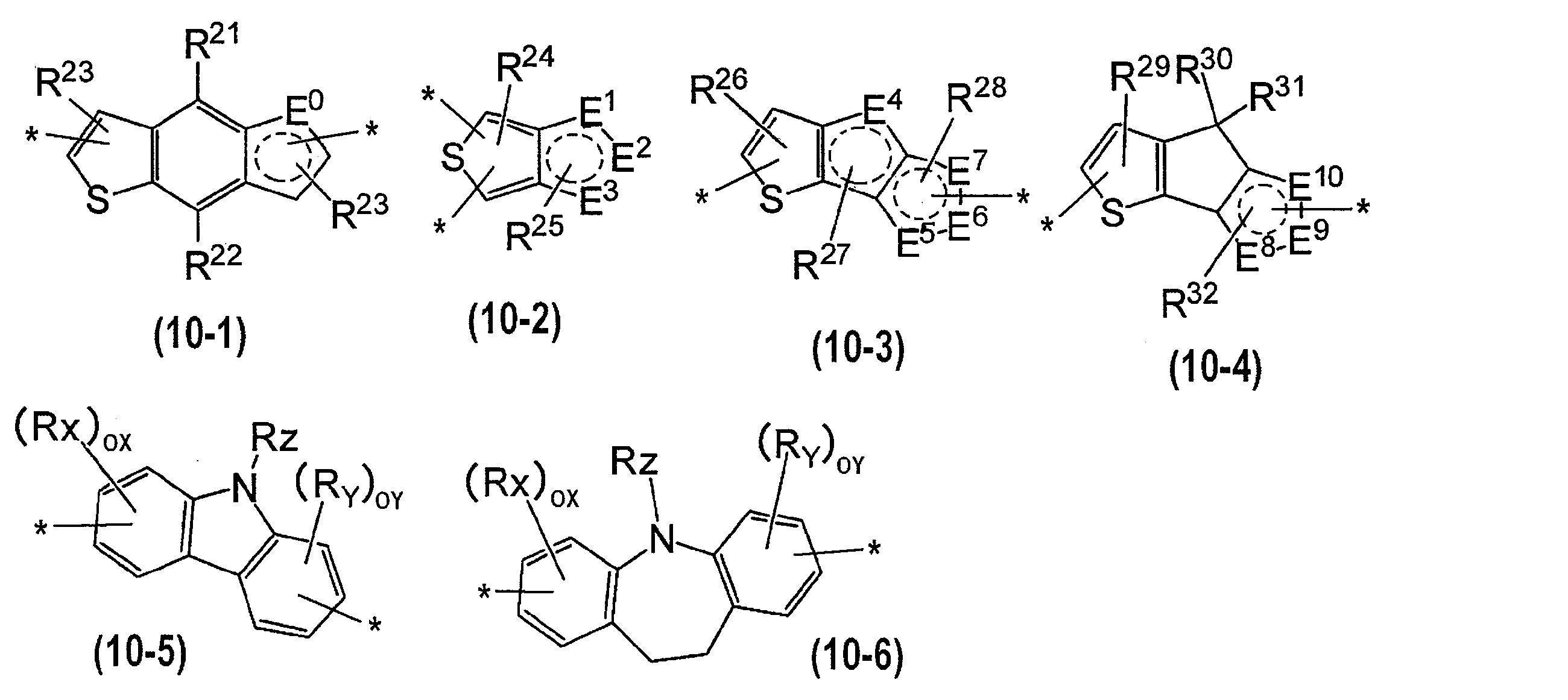
RWの置換基の例としては、置換基Tが挙げられる。


アルキル基(好ましくは炭素原子数1~20のアルキル基、例えばメチル、エチル、イソプロピル、t-ブチル、ペンチル、ヘプチル、1-エチルペンチル、ベンジル、2-エトキシエチル、1-カルボキシメチル等)、アルケニル基(好ましくは炭素原子数2~20のアルケニル基、例えば、ビニル、アリル、オレイル等)、アルキニル基(好ましくは炭素原子数2~20のアルキニル基、例えば、エチニル、ブタジイニル、フェニルエチニル等)、シクロアルキル基(好ましくは炭素原子数3~20のシクロアルキル基、例えば、シクロプロピル、シクロペンチル、シクロヘキシル、4-メチルシクロヘキシル等)、アリール基(好ましくは炭素原子数6~26のアリール基、例えば、フェニル、1-ナフチル、4-メトキシフェニル、2-クロロフェニル、3-メチルフェニル等)、ヘテロ環基(好ましくは炭素原子数2~20のヘテロ環基、例えば、2-ピリジル、4-ピリジル、2-イミダゾリル、2-ベンゾイミダゾリル、2-チアゾリル、2-オキサゾリル等)、アルコキシ基(好ましくは炭素原子数1~20のアルコキシ基、例えば、メトキシ、エトキシ、イソプロピルオキシ、ベンジルオキシ等)、アリールオキシ基(好ましくは炭素原子数6~26のアリールオキシ基、例えば、フェノキシ、1-ナフチルオキシ、3-メチルフェノキシ、4-メトキシフェノキシ等)、アルコキシカルボニル基(好ましくは炭素原子数2~20のアルコキシカルボニル基、例えば、エトキシカルボニル、2-エチルヘキシルオキシカルボニル等)、アミノ基(好ましくは炭素原子数0~20のアミノ基、例えば、アミノ、N,N-ジメチルアミノ、N,N-ジエチルアミノ、N-エチルアミノ、アニリノ等)、スルホンアミド基(好ましくは炭素原子数0~20のスルホンアミド基、例えば、N,N-ジメチルスルホンアミド、N-フェニルスルホンアミド等)、アシルオキシ基(好ましくは炭素原子数1~20のアシルオキシ基、例えば、アセチルオキシ、ベンゾイルオキシ等)、カルバモイル基(好ましくは炭素原子数1~20のカルバモイル基、例えば、N,N-ジメチルカルバモイル、N-フェニルカルバモイル等)、アシルアミノ基(好ましくは炭素原子数1~20のアシルアミノ基、例えば、アセチルアミノ、ベンゾイルアミノ等)、シアノ基、又はハロゲン原子(例えばフッ素原子、塩素原子、臭素原子、ヨウ素原子等)であり、より好ましくはアルキル基、アルケニル基、アリール基、ヘテロ環基、アルコキシ基、アリールオキシ基、アルコキシカルボニル基、アミノ基、アシルアミノ基、シアノ基又はハロゲン原子であり、特に好ましくはアルキル基、アルケニル基、ヘテロ環基、アルコキシ基、アルコキシカルボニル基、アミノ基、アシルアミノ基又はシアノ基が挙げられる。



本発明の光電変換素子10に用いられる電解質組成物には、酸化還元対として、例えばヨウ素とヨウ化物(例えばヨウ化リチウム、ヨウ化テトラブチルアンモニウム、ヨウ化テトラプロピルアンモニウム等)との組み合わせ、アルキルビオローゲン(例えばメチルビオローゲンクロリド、ヘキシルビオローゲンブロミド、ベンジルビオローゲンテトラフルオロボレート)とその還元体との組み合わせ、ポリヒドロキシベンゼン類(例えばハイドロキノン、ナフトハイドロキノン等)とその酸化体との組み合わせ、2価と3価の鉄錯体(例えば赤血塩と黄血塩)2価と3価のコバルト錯体の組み合わせ等が挙げられる。これらのうちヨウ素とヨウ化物との組み合わせ、2価と3価のコバルト錯体の組み合わせが好ましい。
Co(LL2)m2(X)m3・CI : 式(14)
(式(14)において、LL2は下記式LL2で表される2座又は3座の配位子を表す。Xは1座又は2座の配位子を表す。m2は0~3の整数を表す。m3は0~6の整数を表す。CIは電荷を中和させるのに対イオンが必要な場合の対イオンを表す。)


。より好ましくは1.0~50質量%である。ポリマーの架橋反応により電解質組成物をゲル化させる場合は、組成物に架橋可能な反応性基を有するポリマー及び架橋剤を添加するのが好ましい。好ましい反応性基はピリジン環、イミダゾール環、チアゾール環、オキサゾール環、トリアゾール環、モルホリン環、ピペリジン環、ピペラジン環等の含窒素複素環であり、好ましい架橋剤は窒素原子が求核攻撃できる官能基を2つ以上有する化合物(求電子剤)であり、例えば2官能以上のハロゲン化アルキル、ハロゲン化アラルキル、スルホン酸エステル、酸無水物、酸クロライド、イソシアネート等である。
図1に示すように、本発明の光電変換素子には、導電性支持体1上には多孔質の半導体微粒子22に増感色素21が吸着された感光体層2が形成されている。後述する通り、例えば、半導体微粒子の分散液を導電性支持体に塗布・乾燥後、本発明の色素溶液に浸漬することにより、感光体層2を製造することができる。
図1に示すように、本実施形態の光電変換素子10において、導電性支持体1上には多孔質の半導体微粒子22に増感色素21が吸着された感光体層2が形成されている。後述する通り、例えば、半導体微粒子22の分散液を前記導電性支持体1に塗布・乾燥後、上述の色素溶液に浸漬することにより、感光体層2を製造することができる。
本発明においては、半導体微粒子以外の固形分の含量が、半導体微粒子分散液全体の10質量%以下よりなる半導体微粒子分散液を前記導電性支持体1に塗布し、適度に加熱することにより、多孔質半導体微粒子塗布層を得ることができる。
前記色素が塩である場合、前記特定の金属錯体色素の対イオンは特に限定されず、例えばアルカリ金属イオン又は4級アンモニウムイオン等が挙げられる。
[色素の調製]
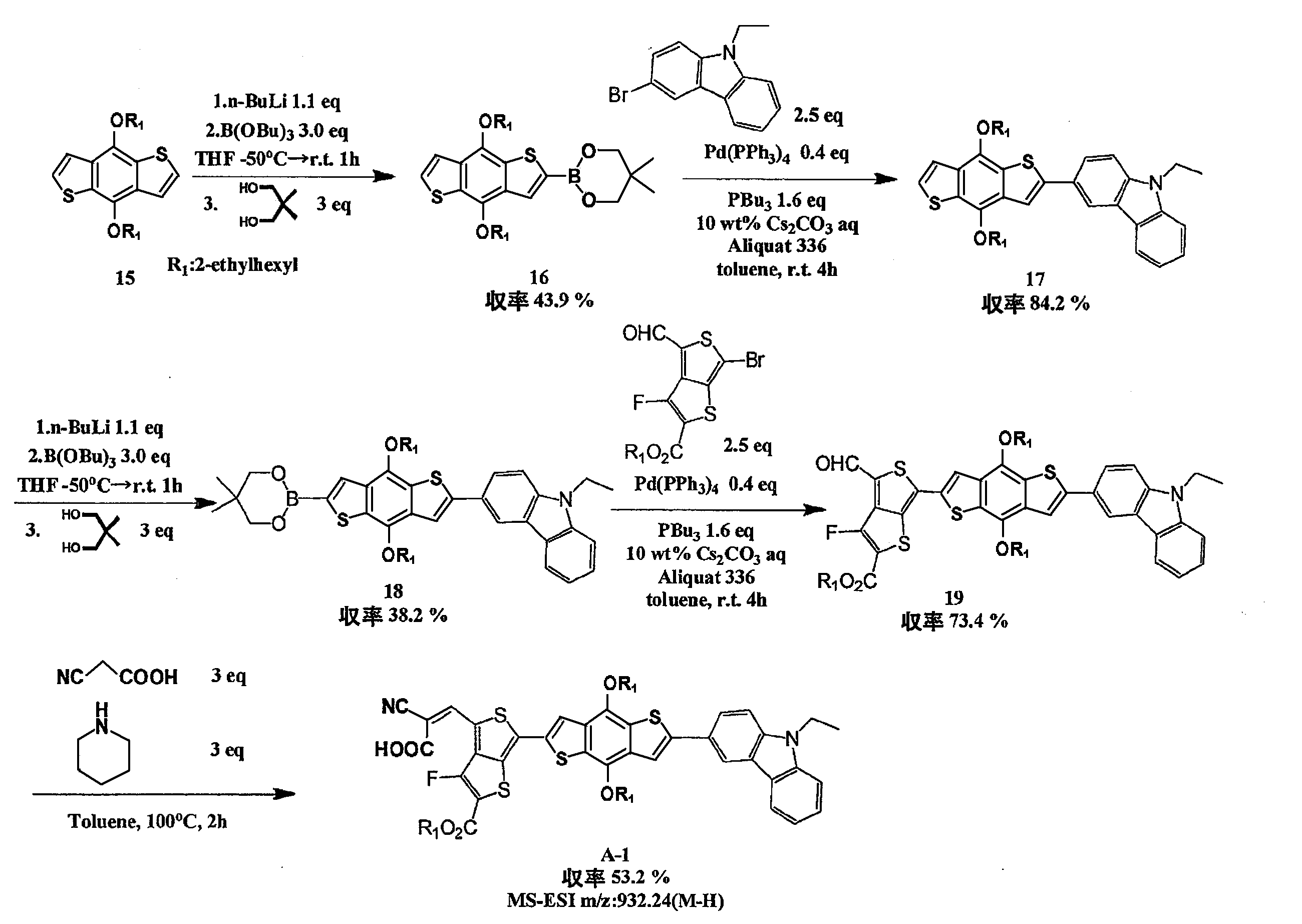
本発明の色素である、A-1を以下に示す方法で調製した。その他の色素も同様の方法で調製した。

色素の極大吸収波長と、長波長端(Abs/Absmax=0.1)を測定した。長波長端とは、溶液吸収スペクトルのλmaxのAbs(Absmax)に対するAbsが10%(Abs/Absmax=0.1)となるときの波長を表す。その結果を表1に示す。測定は、分光光度計(U-4100(商品名)、日立ハイテク社製)によって行い、溶液はTHF:エタノール=1:1を用い、濃度が2μMになるように調整した。
上記の方法で及び同様の方法で調製した表1記載の色素について、d部分とa部分のHOMOとLUMOのエネルギー順位を計算するとともに、d部分とa部分のHOMOのエネルギー順位の差を、Winmostar計算ソフト(Winmostar(商品名)、株式会社テンキューブ研究所製)で計算した。その結果を表1に示す。
ガラス基板上にFTO膜を形成することにより、透明導電膜を作製した。その後透明導電膜上に半導体微粒子層を形成することにより、透明電極板を得た。そしてその透明電極板を使用して光電気化学電池を作製し、変換効率を測定した。その方法は以下の(1)~(3)の通りである。
(1)FTO(フッ素ドープ酸化スズ)膜用原料化合物溶液の調製
塩化スズ(IV)五水和物0.701gをエタノール10mLに溶解し、これにフッ化アンモニウム0.592gの飽和水溶液を加え、この混合物を超音波洗浄機に約20分間かけ、完全に溶解して、FTO膜用原料化合物溶液とした。
(2)FTO透明導電膜の作製
厚さ2mmの耐熱ガラス板の表面を化学洗浄し、乾燥した後、このガラス板を反応器内に置き、ヒータで加熱した。ヒータの加熱温度が450℃になったところで、(1)で得られたFTO膜用原料化合物溶液を、口径0.3mmのノズルから圧力0.06MPaで、ガラス板までの距離を400mmとして、25分間噴霧した。これにより、耐熱ガラス板上に厚さ170nmのFTO膜が形成された透明電極板が得られた。その後、透明電極板を加熱炉にて、450℃で2時間加熱した。
次に、透明電極板を用いて、特許第4260494号公報の図2に示した構造の光電気化学電池を作製した。酸化物半導体多孔質膜の形成は、平均粒径約7nmの酸化チタン微粒子をアセトニトリルに分散してペーストとし、これを透明電極11上にバーコート法により塗布し、乾燥後450℃で1時間焼成して行った。その後、さらに平均粒径約400nmの酸化チタン微粒子のアセトニトリルペースト液を塗布し、これを透明電極11上にバーコート法により塗布し、乾燥後450℃で1時間焼成して行い、厚さ 15 μmの厚さの半導体微粒子層を形成した。
A:500時間光照射後の変換効率が初期値の80%以上のもの
B:80%未満で60%以上のもの
C:60%未満で40%以上のものを
D:40%未満で20%以上のものを
E:20%未満のもの%をEとした。


下記試験201~204、C21~C24は、色素として表中のものを用い、電解質をヨウ素から表中記載のものに変更した以外は試験101~110と同様にして行ったものである。
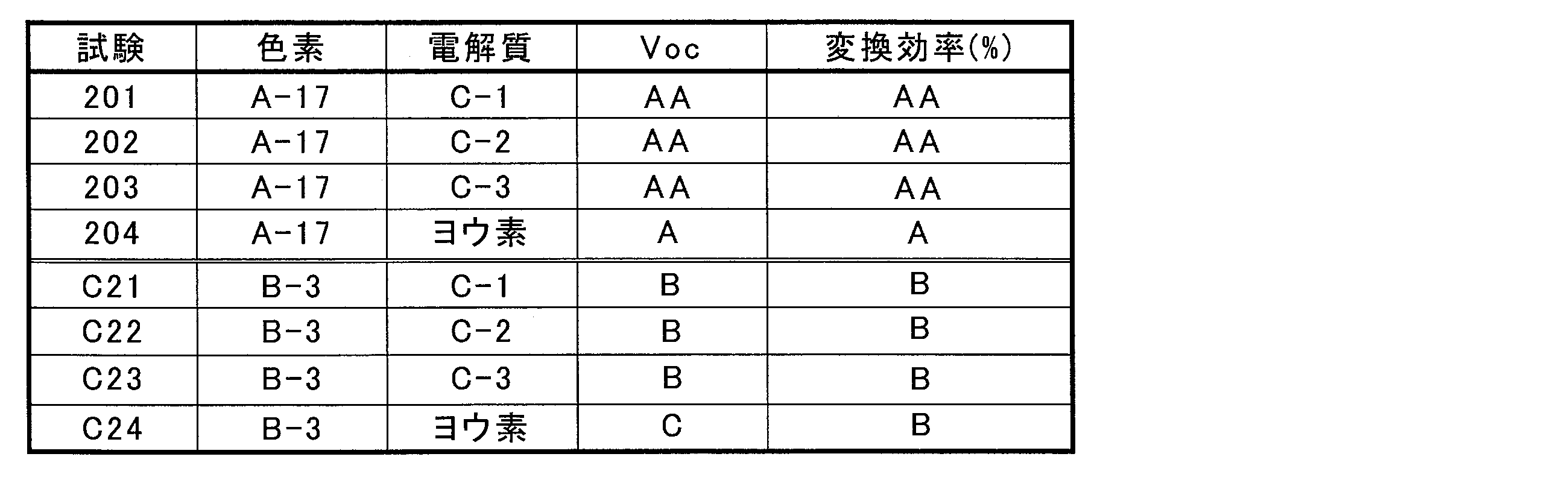
上記の結果は相対評価で示しており、それぞれ以下の意味である。
AA: Very Good
A: Good
B: Normal
C: Inferior to Normal
2 感光体層
21 増感色素
22 半導体微粒子
3 電荷移動体層
4 対極
5 受光電極
6 外部回路
10 光電変換素子
100 光電気化学電池システム
Claims (14)
- 下記式(1)又は(2)で表される化合物よりなる色素。

- 前記色素のd及びaが、Winmostar計算ソフトによる分子軌道計算でLUMOが-3.0~0eV、HOMOが-9.5~-6.0eVである請求項1記載の色素。
- 前記式(1)及び(2)において、前記dとaのうち、Winmostar計算ソフトによる分子軌道計算でHOMOのエネルギー順位の高い基をd、他方をaとし、HOMOのエネルギー順位の差は0.01~1.0eVである請求項1又は2記載の色素。
- 前記式(1)又は(2)のRaRbN-Ar-が下記式(7)で表される請求項1~3のいずれか1項記載の色素。

- 前記式(1)又は(2)のRaRbN-Ar-が下記式(8)で表される請求項1~4のいずれか1項記載の色素。

- 前記式(1)又は(2)のRaRbN-Ar-が下記式(9)で表され、前記d及びaが下記式(10-1)~(10-6)のいずれかで表される請求項1~5のいずれか1項記載の色素。

- 前記Aが下記式(11-1)~(11-5)のいずれかで表される請求項1~6のいずれか1項記載の色素。
- 前記式(1)又は、(2)のRaRbN-Ar-が下記式(12-1)~(12-5)のいずれかで表され、前記d及びaが下記式(13-1)~(13-9)のいずれかで表される請求項1~7のいずれか1項記載の色素。


- 導電性支持体、半導体微粒子と増感色素とを有する感光体層、電解質を有する電荷移動体層、及び対極をその順序で具備する光電変換素子であって、請求項1~8のいずれか1項記載の色素を前記感光体層中の増感色素として用いる光電変換素子。
- 請求項9に記載の光電変換素子を備える光電気化学電池。
- 前記電荷移動体層中の電解質がコバルト錯体である請求項9に記載の光電変換素子。
- 前記コバルト錯体が式(14)で表される請求項11に記載の光電変換素子。
Co(LL2)m2(X)m3・CI : 式(14)
[式(14)において、LL2は下記式LL2で表される2座又は3座の配位子を表す。Xは1座又は2座の配位子を表す。m2は0~3の整数を表す。m3は0~6の整数を表す。CIは電荷を中和させるのに対イオンが必要な場合の対イオンを表す。]

- Xがハロゲン原子であることを特徴とした請求項11又は12記載の光電気変換素子。
- 式(14)中のLL2が下記式(14-1)~(14-3)で表される請求項11~13のいずれかに記載の光電変換素子。
Priority Applications (1)
| Application Number | Priority Date | Filing Date | Title |
|---|---|---|---|
| GB1319073.1A GB2507661A (en) | 2011-03-31 | 2012-02-29 | Pigment, photoelectric converter, and photoelectrochemical cell |
Applications Claiming Priority (4)
| Application Number | Priority Date | Filing Date | Title |
|---|---|---|---|
| JP2011081209 | 2011-03-31 | ||
| JP2011-081209 | 2011-03-31 | ||
| JP2011177756A JP5771092B2 (ja) | 2011-03-31 | 2011-08-15 | 色素、光電変換素子及び光電気化学電池 |
| JP2011-177756 | 2011-08-15 |
Publications (1)
| Publication Number | Publication Date |
|---|---|
| WO2012132735A1 true WO2012132735A1 (ja) | 2012-10-04 |
Family
ID=46930482
Family Applications (1)
| Application Number | Title | Priority Date | Filing Date |
|---|---|---|---|
| PCT/JP2012/055111 Ceased WO2012132735A1 (ja) | 2011-03-31 | 2012-02-29 | 色素、光電変換素子及び光電気化学電池 |
Country Status (3)
| Country | Link |
|---|---|
| JP (1) | JP5771092B2 (ja) |
| GB (1) | GB2507661A (ja) |
| WO (1) | WO2012132735A1 (ja) |
Cited By (2)
| Publication number | Priority date | Publication date | Assignee | Title |
|---|---|---|---|---|
| CN102838881A (zh) * | 2012-10-07 | 2012-12-26 | 复旦大学 | 基于噻唑衍生物的纯有机染料及其制备方法与应用 |
| EP2915831A4 (en) * | 2012-11-01 | 2016-08-17 | Toshiba Kk | POLYMER, ORGANIC THIN-FILM SOLAR CELL WITH IT AND ELECTRONIC DEVICE WITH THIS SOLAR CELL |
Families Citing this family (5)
| Publication number | Priority date | Publication date | Assignee | Title |
|---|---|---|---|---|
| KR101769665B1 (ko) * | 2014-03-27 | 2017-08-21 | 주식회사 엘지화학 | 헤테로환 화합물 및 이를 포함하는 유기 태양 전지 |
| JP6297891B2 (ja) * | 2014-04-01 | 2018-03-20 | 株式会社リコー | 有機材料及び光電変換素子 |
| US10249910B2 (en) | 2014-07-18 | 2019-04-02 | Board Of Trustees Of Michigan State University | Rechargeable lithium-ion cell |
| JP7089295B2 (ja) | 2016-11-22 | 2022-06-22 | ボード オブ トラスティーズ オブ ミシガン ステイト ユニバーシティ | 充電式電気化学セルおよび酸化還元フロー電池 |
| JP6985763B2 (ja) * | 2017-07-20 | 2021-12-22 | ボード オブ トラスティーズ オブ ミシガン ステイト ユニバーシティBoard Of Trustees Of Michigan State University | レドックスフロー電池のための活物質 |
Citations (5)
| Publication number | Priority date | Publication date | Assignee | Title |
|---|---|---|---|---|
| JP2001291534A (ja) * | 2000-01-31 | 2001-10-19 | Fuji Photo Film Co Ltd | 光電変換素子および光電池ならびに金属錯体色素 |
| WO2009098643A2 (en) * | 2008-02-04 | 2009-08-13 | Ecole polytechnique fédérale de Lausanne (EPFL) | Organic sensitizers |
| JP2010235908A (ja) * | 2008-10-29 | 2010-10-21 | Fujifilm Corp | 色素、これを用いた光電変換素子及び光電気化学電池 |
| JP2010265458A (ja) * | 2009-05-15 | 2010-11-25 | Ind Technol Res Inst | 有機色素および光電変換装置 |
| JP2011026376A (ja) * | 2009-07-21 | 2011-02-10 | Fujifilm Corp | 色素、これを用いた光電変換素子及び光電気化学電池 |
Family Cites Families (2)
| Publication number | Priority date | Publication date | Assignee | Title |
|---|---|---|---|---|
| WO2003038508A2 (en) * | 2001-10-30 | 2003-05-08 | Colorado State University Research Foundation | Metal complex-based electron-transfer mediators in dye-sensitized solar cells |
| KR100969675B1 (ko) * | 2007-05-25 | 2010-08-17 | 주식회사 동진쎄미켐 | 신규한 엔-아릴카바졸 잔기-함유 유기염료 및 이의제조방법 |
-
2011
- 2011-08-15 JP JP2011177756A patent/JP5771092B2/ja not_active Expired - Fee Related
-
2012
- 2012-02-29 WO PCT/JP2012/055111 patent/WO2012132735A1/ja not_active Ceased
- 2012-02-29 GB GB1319073.1A patent/GB2507661A/en not_active Withdrawn
Patent Citations (5)
| Publication number | Priority date | Publication date | Assignee | Title |
|---|---|---|---|---|
| JP2001291534A (ja) * | 2000-01-31 | 2001-10-19 | Fuji Photo Film Co Ltd | 光電変換素子および光電池ならびに金属錯体色素 |
| WO2009098643A2 (en) * | 2008-02-04 | 2009-08-13 | Ecole polytechnique fédérale de Lausanne (EPFL) | Organic sensitizers |
| JP2010235908A (ja) * | 2008-10-29 | 2010-10-21 | Fujifilm Corp | 色素、これを用いた光電変換素子及び光電気化学電池 |
| JP2010265458A (ja) * | 2009-05-15 | 2010-11-25 | Ind Technol Res Inst | 有機色素および光電変換装置 |
| JP2011026376A (ja) * | 2009-07-21 | 2011-02-10 | Fujifilm Corp | 色素、これを用いた光電変換素子及び光電気化学電池 |
Non-Patent Citations (1)
| Title |
|---|
| PING SHEN ET AL.: "Efficient triphenylamine- based dyes featuring dual-role carbazole, fluorene and spirobifluorene moieties", ORGANIC ELECTRONICS, vol. 12, January 2011 (2011-01-01), pages 125 - 135, XP027576996 * |
Cited By (4)
| Publication number | Priority date | Publication date | Assignee | Title |
|---|---|---|---|---|
| CN102838881A (zh) * | 2012-10-07 | 2012-12-26 | 复旦大学 | 基于噻唑衍生物的纯有机染料及其制备方法与应用 |
| CN102838881B (zh) * | 2012-10-07 | 2014-12-03 | 复旦大学 | 基于噻唑衍生物的纯有机染料及其制备方法与应用 |
| EP2915831A4 (en) * | 2012-11-01 | 2016-08-17 | Toshiba Kk | POLYMER, ORGANIC THIN-FILM SOLAR CELL WITH IT AND ELECTRONIC DEVICE WITH THIS SOLAR CELL |
| US9865831B2 (en) | 2012-11-01 | 2018-01-09 | Kabushiki Kaisha Toshiba | Polymer, organic thin-film solar cell using the same, and electronic product comprising the cell |
Also Published As
| Publication number | Publication date |
|---|---|
| JP2012214671A (ja) | 2012-11-08 |
| GB2507661A (en) | 2014-05-07 |
| GB201319073D0 (en) | 2013-12-11 |
| GB2507661A8 (en) | 2016-01-20 |
| JP5771092B2 (ja) | 2015-08-26 |
Similar Documents
| Publication | Publication Date | Title |
|---|---|---|
| JP4363553B2 (ja) | 電解質組成物、光電変換素子および光電気化学電池 | |
| JP5771092B2 (ja) | 色素、光電変換素子及び光電気化学電池 | |
| JP5869481B2 (ja) | 金属錯体色素、光電変換素子及び光電気化学電池 | |
| CN103764768B (zh) | 色素与其制造方法、光电转换元件及光电化学电池、以及三联吡啶化合物与其制造方法 | |
| JP5620496B2 (ja) | 金属錯体色素、光電変換素子及び光電気化学電池 | |
| JP5649368B2 (ja) | 光電変換素子及び光電気化学電池 | |
| JP5809870B2 (ja) | 光電変換素子、光電気化学電池、及びそれらに用いられる色素 | |
| JP2011228276A (ja) | 光電変換素子及び光電気化学電池 | |
| JP5816111B2 (ja) | 金属錯体色素組成物、光電変換素子及び光電気化学電池 | |
| JP5756772B2 (ja) | 光電変換素子及び光電気化学電池 | |
| US20130118570A1 (en) | Dye for photoelectric conversion, semiconductor electrode, photoelectric conversion element, solar cell, and novel pyrroline-based compound | |
| WO2012017873A1 (ja) | 金属錯体色素、光電変換素子及び光電気化学電池 | |
| JP5756766B2 (ja) | 光電変換素子、光電気化学電池及び色素 | |
| WO2011108611A1 (ja) | 光電変換素子及び光電気化学電池 | |
| JP5636317B2 (ja) | 金属錯体色素、金属錯体色素組成物、光電変換素子及び光電気化学電池 | |
| WO2015002081A1 (ja) | 光電変換素子、色素増感太陽電池、金属錯体色素、配位子、色素溶液、色素吸着電極および色素増感太陽電池の製造方法 | |
| JP5572027B2 (ja) | 光電変換素子及びこれに用いられる光電変換素子用組成物 | |
| WO2011108613A1 (ja) | 光電変換素子及び光電気化学電池 | |
| WO2016047344A1 (ja) | 光電変換素子、色素増感太陽電池、金属錯体色素および色素溶液 |
Legal Events
| Date | Code | Title | Description |
|---|---|---|---|
| 121 | Ep: the epo has been informed by wipo that ep was designated in this application |
Ref document number: 12763089 Country of ref document: EP Kind code of ref document: A1 |
|
| NENP | Non-entry into the national phase |
Ref country code: DE |
|
| ENP | Entry into the national phase |
Ref document number: 1319073 Country of ref document: GB Kind code of ref document: A Free format text: PCT FILING DATE = 20120229 |
|
| WWE | Wipo information: entry into national phase |
Ref document number: 1319073.1 Country of ref document: GB |
|
| 122 | Ep: pct application non-entry in european phase |
Ref document number: 12763089 Country of ref document: EP Kind code of ref document: A1 |