WO2012132616A1 - Procédé de fabrication d'un élément de conversion photoélectrique - Google Patents
Procédé de fabrication d'un élément de conversion photoélectrique Download PDFInfo
- Publication number
- WO2012132616A1 WO2012132616A1 PCT/JP2012/053851 JP2012053851W WO2012132616A1 WO 2012132616 A1 WO2012132616 A1 WO 2012132616A1 JP 2012053851 W JP2012053851 W JP 2012053851W WO 2012132616 A1 WO2012132616 A1 WO 2012132616A1
- Authority
- WO
- WIPO (PCT)
- Prior art keywords
- layer
- photoelectric conversion
- conversion element
- amorphous silicon
- type amorphous
- Prior art date
Links
- 238000006243 chemical reaction Methods 0.000 title claims abstract description 72
- 238000004519 manufacturing process Methods 0.000 title claims abstract description 59
- 238000000034 method Methods 0.000 claims abstract description 64
- 239000004065 semiconductor Substances 0.000 claims abstract description 44
- 239000000758 substrate Substances 0.000 claims abstract description 44
- 229920002120 photoresistant polymer Polymers 0.000 claims abstract description 34
- 238000005530 etching Methods 0.000 claims description 21
- 229910052581 Si3N4 Inorganic materials 0.000 claims description 3
- VYPSYNLAJGMNEJ-UHFFFAOYSA-N Silicium dioxide Chemical compound O=[Si]=O VYPSYNLAJGMNEJ-UHFFFAOYSA-N 0.000 claims description 3
- PMHQVHHXPFUNSP-UHFFFAOYSA-M copper(1+);methylsulfanylmethane;bromide Chemical compound Br[Cu].CSC PMHQVHHXPFUNSP-UHFFFAOYSA-M 0.000 claims description 3
- HQVNEWCFYHHQES-UHFFFAOYSA-N silicon nitride Chemical compound N12[Si]34N5[Si]62N3[Si]51N64 HQVNEWCFYHHQES-UHFFFAOYSA-N 0.000 claims description 3
- 229910052814 silicon oxide Inorganic materials 0.000 claims description 3
- 229910021421 monocrystalline silicon Inorganic materials 0.000 abstract description 32
- 239000010410 layer Substances 0.000 description 222
- 229910021417 amorphous silicon Inorganic materials 0.000 description 99
- KWYUFKZDYYNOTN-UHFFFAOYSA-M Potassium hydroxide Chemical compound [OH-].[K+] KWYUFKZDYYNOTN-UHFFFAOYSA-M 0.000 description 20
- 239000010408 film Substances 0.000 description 19
- 229910052751 metal Inorganic materials 0.000 description 15
- 239000002184 metal Substances 0.000 description 15
- 239000000243 solution Substances 0.000 description 13
- HEMHJVSKTPXQMS-UHFFFAOYSA-M Sodium hydroxide Chemical compound [OH-].[Na+] HEMHJVSKTPXQMS-UHFFFAOYSA-M 0.000 description 12
- 239000007864 aqueous solution Substances 0.000 description 11
- 239000002019 doping agent Substances 0.000 description 9
- 238000005268 plasma chemical vapour deposition Methods 0.000 description 8
- 238000007747 plating Methods 0.000 description 8
- 238000000059 patterning Methods 0.000 description 6
- 238000004544 sputter deposition Methods 0.000 description 6
- 238000010248 power generation Methods 0.000 description 5
- 239000003513 alkali Substances 0.000 description 4
- 239000010949 copper Substances 0.000 description 4
- 239000010409 thin film Substances 0.000 description 4
- 239000013078 crystal Substances 0.000 description 3
- 238000002161 passivation Methods 0.000 description 3
- 238000007650 screen-printing Methods 0.000 description 3
- JBRZTFJDHDCESZ-UHFFFAOYSA-N AsGa Chemical compound [As]#[Ga] JBRZTFJDHDCESZ-UHFFFAOYSA-N 0.000 description 2
- RYGMFSIKBFXOCR-UHFFFAOYSA-N Copper Chemical compound [Cu] RYGMFSIKBFXOCR-UHFFFAOYSA-N 0.000 description 2
- 229910001218 Gallium arsenide Inorganic materials 0.000 description 2
- 230000002378 acidificating effect Effects 0.000 description 2
- 230000015572 biosynthetic process Effects 0.000 description 2
- 239000000969 carrier Substances 0.000 description 2
- 229910052802 copper Inorganic materials 0.000 description 2
- 239000000428 dust Substances 0.000 description 2
- 230000005611 electricity Effects 0.000 description 2
- AMGQUBHHOARCQH-UHFFFAOYSA-N indium;oxotin Chemical compound [In].[Sn]=O AMGQUBHHOARCQH-UHFFFAOYSA-N 0.000 description 2
- 239000011241 protective layer Substances 0.000 description 2
- GPXJNWSHGFTCBW-UHFFFAOYSA-N Indium phosphide Chemical compound [In]#P GPXJNWSHGFTCBW-UHFFFAOYSA-N 0.000 description 1
- 229910006404 SnO 2 Inorganic materials 0.000 description 1
- ATJFFYVFTNAWJD-UHFFFAOYSA-N Tin Chemical compound [Sn] ATJFFYVFTNAWJD-UHFFFAOYSA-N 0.000 description 1
- GWEVSGVZZGPLCZ-UHFFFAOYSA-N Titan oxide Chemical compound O=[Ti]=O GWEVSGVZZGPLCZ-UHFFFAOYSA-N 0.000 description 1
- XLOMVQKBTHCTTD-UHFFFAOYSA-N Zinc monoxide Chemical compound [Zn]=O XLOMVQKBTHCTTD-UHFFFAOYSA-N 0.000 description 1
- 230000002411 adverse Effects 0.000 description 1
- 229910045601 alloy Inorganic materials 0.000 description 1
- 239000000956 alloy Substances 0.000 description 1
- 238000005229 chemical vapour deposition Methods 0.000 description 1
- 238000010292 electrical insulation Methods 0.000 description 1
- 238000009713 electroplating Methods 0.000 description 1
- 229910003437 indium oxide Inorganic materials 0.000 description 1
- PJXISJQVUVHSOJ-UHFFFAOYSA-N indium(iii) oxide Chemical compound [O-2].[O-2].[O-2].[In+3].[In+3] PJXISJQVUVHSOJ-UHFFFAOYSA-N 0.000 description 1
- 238000001459 lithography Methods 0.000 description 1
- 239000000463 material Substances 0.000 description 1
- 229910044991 metal oxide Inorganic materials 0.000 description 1
- 150000004706 metal oxides Chemical class 0.000 description 1
- 229910021420 polycrystalline silicon Inorganic materials 0.000 description 1
- XOLBLPGZBRYERU-UHFFFAOYSA-N tin dioxide Chemical compound O=[Sn]=O XOLBLPGZBRYERU-UHFFFAOYSA-N 0.000 description 1
- 229910001887 tin oxide Inorganic materials 0.000 description 1
- 239000012780 transparent material Substances 0.000 description 1
Images


Classifications
-
- H—ELECTRICITY
- H01—ELECTRIC ELEMENTS
- H01L—SEMICONDUCTOR DEVICES NOT COVERED BY CLASS H10
- H01L31/00—Semiconductor devices sensitive to infrared radiation, light, electromagnetic radiation of shorter wavelength or corpuscular radiation and specially adapted either for the conversion of the energy of such radiation into electrical energy or for the control of electrical energy by such radiation; Processes or apparatus specially adapted for the manufacture or treatment thereof or of parts thereof; Details thereof
- H01L31/04—Semiconductor devices sensitive to infrared radiation, light, electromagnetic radiation of shorter wavelength or corpuscular radiation and specially adapted either for the conversion of the energy of such radiation into electrical energy or for the control of electrical energy by such radiation; Processes or apparatus specially adapted for the manufacture or treatment thereof or of parts thereof; Details thereof adapted as photovoltaic [PV] conversion devices
- H01L31/06—Semiconductor devices sensitive to infrared radiation, light, electromagnetic radiation of shorter wavelength or corpuscular radiation and specially adapted either for the conversion of the energy of such radiation into electrical energy or for the control of electrical energy by such radiation; Processes or apparatus specially adapted for the manufacture or treatment thereof or of parts thereof; Details thereof adapted as photovoltaic [PV] conversion devices characterised by potential barriers
- H01L31/068—Semiconductor devices sensitive to infrared radiation, light, electromagnetic radiation of shorter wavelength or corpuscular radiation and specially adapted either for the conversion of the energy of such radiation into electrical energy or for the control of electrical energy by such radiation; Processes or apparatus specially adapted for the manufacture or treatment thereof or of parts thereof; Details thereof adapted as photovoltaic [PV] conversion devices characterised by potential barriers the potential barriers being only of the PN homojunction type, e.g. bulk silicon PN homojunction solar cells or thin film polycrystalline silicon PN homojunction solar cells
- H01L31/0682—Semiconductor devices sensitive to infrared radiation, light, electromagnetic radiation of shorter wavelength or corpuscular radiation and specially adapted either for the conversion of the energy of such radiation into electrical energy or for the control of electrical energy by such radiation; Processes or apparatus specially adapted for the manufacture or treatment thereof or of parts thereof; Details thereof adapted as photovoltaic [PV] conversion devices characterised by potential barriers the potential barriers being only of the PN homojunction type, e.g. bulk silicon PN homojunction solar cells or thin film polycrystalline silicon PN homojunction solar cells back-junction, i.e. rearside emitter, solar cells, e.g. interdigitated base-emitter regions back-junction cells
-
- H—ELECTRICITY
- H01—ELECTRIC ELEMENTS
- H01L—SEMICONDUCTOR DEVICES NOT COVERED BY CLASS H10
- H01L31/00—Semiconductor devices sensitive to infrared radiation, light, electromagnetic radiation of shorter wavelength or corpuscular radiation and specially adapted either for the conversion of the energy of such radiation into electrical energy or for the control of electrical energy by such radiation; Processes or apparatus specially adapted for the manufacture or treatment thereof or of parts thereof; Details thereof
- H01L31/02—Details
- H01L31/0224—Electrodes
- H01L31/022408—Electrodes for devices characterised by at least one potential jump barrier or surface barrier
- H01L31/022425—Electrodes for devices characterised by at least one potential jump barrier or surface barrier for solar cells
- H01L31/022441—Electrode arrangements specially adapted for back-contact solar cells
-
- H—ELECTRICITY
- H01—ELECTRIC ELEMENTS
- H01L—SEMICONDUCTOR DEVICES NOT COVERED BY CLASS H10
- H01L31/00—Semiconductor devices sensitive to infrared radiation, light, electromagnetic radiation of shorter wavelength or corpuscular radiation and specially adapted either for the conversion of the energy of such radiation into electrical energy or for the control of electrical energy by such radiation; Processes or apparatus specially adapted for the manufacture or treatment thereof or of parts thereof; Details thereof
- H01L31/0248—Semiconductor devices sensitive to infrared radiation, light, electromagnetic radiation of shorter wavelength or corpuscular radiation and specially adapted either for the conversion of the energy of such radiation into electrical energy or for the control of electrical energy by such radiation; Processes or apparatus specially adapted for the manufacture or treatment thereof or of parts thereof; Details thereof characterised by their semiconductor bodies
- H01L31/0352—Semiconductor devices sensitive to infrared radiation, light, electromagnetic radiation of shorter wavelength or corpuscular radiation and specially adapted either for the conversion of the energy of such radiation into electrical energy or for the control of electrical energy by such radiation; Processes or apparatus specially adapted for the manufacture or treatment thereof or of parts thereof; Details thereof characterised by their semiconductor bodies characterised by their shape or by the shapes, relative sizes or disposition of the semiconductor regions
- H01L31/035272—Semiconductor devices sensitive to infrared radiation, light, electromagnetic radiation of shorter wavelength or corpuscular radiation and specially adapted either for the conversion of the energy of such radiation into electrical energy or for the control of electrical energy by such radiation; Processes or apparatus specially adapted for the manufacture or treatment thereof or of parts thereof; Details thereof characterised by their semiconductor bodies characterised by their shape or by the shapes, relative sizes or disposition of the semiconductor regions characterised by at least one potential jump barrier or surface barrier
- H01L31/03529—Shape of the potential jump barrier or surface barrier
-
- H—ELECTRICITY
- H01—ELECTRIC ELEMENTS
- H01L—SEMICONDUCTOR DEVICES NOT COVERED BY CLASS H10
- H01L31/00—Semiconductor devices sensitive to infrared radiation, light, electromagnetic radiation of shorter wavelength or corpuscular radiation and specially adapted either for the conversion of the energy of such radiation into electrical energy or for the control of electrical energy by such radiation; Processes or apparatus specially adapted for the manufacture or treatment thereof or of parts thereof; Details thereof
- H01L31/04—Semiconductor devices sensitive to infrared radiation, light, electromagnetic radiation of shorter wavelength or corpuscular radiation and specially adapted either for the conversion of the energy of such radiation into electrical energy or for the control of electrical energy by such radiation; Processes or apparatus specially adapted for the manufacture or treatment thereof or of parts thereof; Details thereof adapted as photovoltaic [PV] conversion devices
- H01L31/06—Semiconductor devices sensitive to infrared radiation, light, electromagnetic radiation of shorter wavelength or corpuscular radiation and specially adapted either for the conversion of the energy of such radiation into electrical energy or for the control of electrical energy by such radiation; Processes or apparatus specially adapted for the manufacture or treatment thereof or of parts thereof; Details thereof adapted as photovoltaic [PV] conversion devices characterised by potential barriers
- H01L31/072—Semiconductor devices sensitive to infrared radiation, light, electromagnetic radiation of shorter wavelength or corpuscular radiation and specially adapted either for the conversion of the energy of such radiation into electrical energy or for the control of electrical energy by such radiation; Processes or apparatus specially adapted for the manufacture or treatment thereof or of parts thereof; Details thereof adapted as photovoltaic [PV] conversion devices characterised by potential barriers the potential barriers being only of the PN heterojunction type
- H01L31/0745—Semiconductor devices sensitive to infrared radiation, light, electromagnetic radiation of shorter wavelength or corpuscular radiation and specially adapted either for the conversion of the energy of such radiation into electrical energy or for the control of electrical energy by such radiation; Processes or apparatus specially adapted for the manufacture or treatment thereof or of parts thereof; Details thereof adapted as photovoltaic [PV] conversion devices characterised by potential barriers the potential barriers being only of the PN heterojunction type comprising a AIVBIV heterojunction, e.g. Si/Ge, SiGe/Si or Si/SiC solar cells
- H01L31/0747—Semiconductor devices sensitive to infrared radiation, light, electromagnetic radiation of shorter wavelength or corpuscular radiation and specially adapted either for the conversion of the energy of such radiation into electrical energy or for the control of electrical energy by such radiation; Processes or apparatus specially adapted for the manufacture or treatment thereof or of parts thereof; Details thereof adapted as photovoltaic [PV] conversion devices characterised by potential barriers the potential barriers being only of the PN heterojunction type comprising a AIVBIV heterojunction, e.g. Si/Ge, SiGe/Si or Si/SiC solar cells comprising a heterojunction of crystalline and amorphous materials, e.g. heterojunction with intrinsic thin layer
-
- H—ELECTRICITY
- H01—ELECTRIC ELEMENTS
- H01L—SEMICONDUCTOR DEVICES NOT COVERED BY CLASS H10
- H01L31/00—Semiconductor devices sensitive to infrared radiation, light, electromagnetic radiation of shorter wavelength or corpuscular radiation and specially adapted either for the conversion of the energy of such radiation into electrical energy or for the control of electrical energy by such radiation; Processes or apparatus specially adapted for the manufacture or treatment thereof or of parts thereof; Details thereof
- H01L31/18—Processes or apparatus specially adapted for the manufacture or treatment of these devices or of parts thereof
- H01L31/20—Processes or apparatus specially adapted for the manufacture or treatment of these devices or of parts thereof such devices or parts thereof comprising amorphous semiconductor materials
- H01L31/202—Processes or apparatus specially adapted for the manufacture or treatment of these devices or of parts thereof such devices or parts thereof comprising amorphous semiconductor materials including only elements of Group IV of the Periodic Table
-
- Y—GENERAL TAGGING OF NEW TECHNOLOGICAL DEVELOPMENTS; GENERAL TAGGING OF CROSS-SECTIONAL TECHNOLOGIES SPANNING OVER SEVERAL SECTIONS OF THE IPC; TECHNICAL SUBJECTS COVERED BY FORMER USPC CROSS-REFERENCE ART COLLECTIONS [XRACs] AND DIGESTS
- Y02—TECHNOLOGIES OR APPLICATIONS FOR MITIGATION OR ADAPTATION AGAINST CLIMATE CHANGE
- Y02E—REDUCTION OF GREENHOUSE GAS [GHG] EMISSIONS, RELATED TO ENERGY GENERATION, TRANSMISSION OR DISTRIBUTION
- Y02E10/00—Energy generation through renewable energy sources
- Y02E10/50—Photovoltaic [PV] energy
- Y02E10/547—Monocrystalline silicon PV cells
-
- Y—GENERAL TAGGING OF NEW TECHNOLOGICAL DEVELOPMENTS; GENERAL TAGGING OF CROSS-SECTIONAL TECHNOLOGIES SPANNING OVER SEVERAL SECTIONS OF THE IPC; TECHNICAL SUBJECTS COVERED BY FORMER USPC CROSS-REFERENCE ART COLLECTIONS [XRACs] AND DIGESTS
- Y02—TECHNOLOGIES OR APPLICATIONS FOR MITIGATION OR ADAPTATION AGAINST CLIMATE CHANGE
- Y02P—CLIMATE CHANGE MITIGATION TECHNOLOGIES IN THE PRODUCTION OR PROCESSING OF GOODS
- Y02P70/00—Climate change mitigation technologies in the production process for final industrial or consumer products
- Y02P70/50—Manufacturing or production processes characterised by the final manufactured product
Definitions
- the present invention relates to a method for manufacturing a photoelectric conversion element.
- Patent Document 1 discloses a semiconductor substrate having a light receiving surface and a back surface provided on the opposite side of the light receiving surface, a first semiconductor layer formed along a predetermined direction on the back surface, and a predetermined direction on the back surface. And a pair of second semiconductor layers disposed on both sides of the first semiconductor layer, and formed from one second semiconductor layer to the first semiconductor layer of the pair of second semiconductor layers.
- the photoelectric conversion element provided with the transparent electrode layer which covers and the collection electrode layer formed on a transparent electrode layer is disclosed.
- an insulating layer or the like may be stacked on a semiconductor layer formed on a semiconductor substrate.
- pinholes may be formed in the insulating layer or the like due to dust or the like in the film forming apparatus.
- the film quality may be adversely affected, for example, the semiconductor layer may be etched through the pinhole.
- an amorphous semiconductor layer is formed on the back surface of a semiconductor substrate, an insulating layer is formed on the amorphous semiconductor layer, and a photoresist is formed on the insulating layer. Forming a layer, and etching the light-receiving surface opposite to the back surface of the semiconductor substrate in a state where the photoresist layer is formed on the insulating layer.
- the power generation characteristics of the photoelectric conversion element can be improved.
- it is sectional drawing of a photoelectric conversion element.
- it is a flowchart which shows the procedure of the manufacturing method of a photoelectric conversion element.
- it is sectional drawing for demonstrating the procedure of the manufacturing method of a photoelectric conversion element.
- it is sectional drawing for demonstrating the procedure of the manufacturing method of a photoelectric conversion element.
- it is sectional drawing for demonstrating the procedure of the manufacturing method of a photoelectric conversion element.
- it is sectional drawing for demonstrating the procedure of the manufacturing method of a photoelectric conversion element.
- it is sectional drawing for demonstrating the procedure of the manufacturing method of a photoelectric conversion element.
- it is sectional drawing for demonstrating the procedure of the manufacturing method of a photoelectric conversion element. In embodiment which concerns on this invention, it is sectional drawing for demonstrating the procedure of the manufacturing method of a photoelectric conversion element. In embodiment which concerns on this invention, it is sectional drawing for demonstrating the procedure of the manufacturing method of a photoelectric conversion element. In embodiment which concerns on this invention, it is sectional drawing for demonstrating the procedure of the manufacturing method of a photoelectric conversion element. In embodiment which concerns on this invention, it is sectional drawing for demonstrating the procedure of the manufacturing method of a photoelectric conversion element. In embodiment which concerns on this invention, it is sectional drawing for demonstrating the procedure of the manufacturing method of a photoelectric conversion element. In embodiment which concerns on this invention, it is sectional drawing for demonstrating the procedure of the manufacturing method of a photoelectric conversion element.
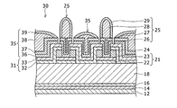
- FIG. 1 is a cross-sectional view of the photoelectric conversion element 10.
- the photoelectric conversion element 10 includes an antireflection layer 12, an n-type amorphous silicon layer 14, an i-type amorphous silicon layer 16, an n-type single crystal silicon substrate 18, an i-n stacked portion 21, and i.
- an arrow A shown in FIG. 1 indicates a direction in which light such as sunlight enters the photoelectric conversion element 10.
- the “light receiving surface” means a surface on which light such as sunlight is mainly incident.
- the “back surface” means a surface opposite to the light receiving surface.
- the n-type single crystal silicon substrate 18 is a power generation layer that receives carriers incident from the light receiving surface and generates carriers.
- the n-type single crystal silicon substrate 18 is used.
- the present invention is not limited to this, and an n-type or p-type conductive crystal semiconductor substrate can be used.
- a polycrystalline silicon substrate, a gallium arsenide substrate (GaAs), an indium phosphorus substrate (InP), or the like can be used.
- the i-type amorphous silicon layer 16 is a passivation layer formed on the light-receiving surface of the n-type single crystal silicon substrate 18.
- the n-type amorphous silicon layer 14 is formed on the i-type amorphous silicon layer 16.
- the i-type amorphous silicon layer 16 and the n-type amorphous silicon layer 14 constitute an amorphous semiconductor layer portion formed on the light receiving surface.
- the i-type amorphous silicon layer 16 is a layer made of an intrinsic amorphous semiconductor film.
- the i-type amorphous silicon layer 16 has a lower dopant concentration in the film than the n-type amorphous silicon layer 14.
- the i-type amorphous silicon layer 16 preferably has an n-type or p-type conductivity of 10 ⁇ 11 s / cm or less.
- the n-type amorphous silicon layer 14 is a layer made of an amorphous semiconductor film containing an n-type conductive dopant.
- the n-type amorphous silicon layer 14 has a higher dopant concentration in the film than the i-type amorphous silicon layer 16.
- the n-type amorphous silicon layer 14 preferably has an n-type conductivity of 10 ⁇ 3 s / cm or more.
- the amorphous silicon layer includes a microcrystalline semiconductor film.
- a microcrystalline semiconductor film is a film in which crystal grains are precipitated in an amorphous semiconductor.
- the average grain size of the crystal grains is not limited to this, but is estimated to be about 1 nm to 80 nm.
- the antireflection layer 12 is formed on the n-type amorphous silicon layer 14 and reduces reflection of light incident from the light receiving surface of the photoelectric conversion element 10.
- the antireflection layer 12 also functions as a protective layer that protects the surface of the n-type amorphous silicon layer 14.
- the antireflection layer 12 is made of a transparent material and has a refractive index that reduces reflection of light incident from the light receiving surface of the photoelectric conversion element 10 in relation to the refractive index of the layer covered by the antireflection layer 12. And a film thickness is preferred.
- the antireflection layer 12 includes, for example, aluminum nitride, silicon nitride, silicon oxide, and the like.
- the i-n laminated portion 21 is formed on the back surface of the n-type single crystal silicon substrate 18. It is preferable that the i-n stacked unit 21 is arranged so that current can be collected evenly from the surface of the photoelectric conversion element 10 in an n-side electrode unit 25 described later.
- the i-n stacked portion 21 preferably has a comb-teeth shape in which a plurality of finger portions extend in parallel.
- the i-n stacked unit 21 includes an i-type amorphous silicon layer 22 and an n-type amorphous silicon layer 23.
- the i-type amorphous silicon layer 22 is a passivation layer formed on the back surface of the n-type single crystal silicon substrate 18.
- the n-type amorphous silicon layer 23 is formed on the i-type amorphous silicon layer 22.
- the i-type amorphous silicon layer 22 and the n-type amorphous silicon layer 23 constitute a first amorphous semiconductor layer portion formed on the back surface.
- the i-type amorphous silicon layer 22 is a layer made of an intrinsic amorphous semiconductor film.
- the i-type amorphous silicon layer 22 has a lower dopant concentration in the film than the n-type amorphous silicon layer 23.
- the i-type amorphous silicon layer 22 preferably has an n-type or p-type conductivity of 10 ⁇ 11 s / cm or less.
- the n-type amorphous silicon layer 23 is a layer made of an amorphous semiconductor film containing an n-type conductive dopant.
- the n-type amorphous silicon layer 23 has a higher dopant concentration in the film than the i-type amorphous silicon layer 22.
- the n-type amorphous silicon layer 23 preferably has an n-type conductivity of 10 ⁇ 3 s / cm or more.
- the insulating layer 24 is formed to electrically insulate the i-n laminated portion 21 and the ip laminated portion 31.
- the insulating layer 24 also functions as a protective layer formed on the n-type amorphous silicon layer 23.
- the insulating layer 24 may be any material having electrical insulation properties, but preferably includes, for example, aluminum nitride, silicon nitride, silicon oxide, and the like.
- the n-side electrode portion 25 is an electrode member provided for collecting and taking out the electricity generated in the photoelectric conversion element 10.
- the n-side electrode unit 25 includes a transparent conductive layer 26, a metal layer 27, a first electrode unit 28, and a second electrode unit 29.
- the transparent conductive layer 26 is formed on the n-type amorphous silicon layer 23.
- the transparent conductive layer 26 is made of a metal oxide such as indium oxide (In 2 O 3 ), zinc oxide (ZnO), tin oxide (SnO 2 ), titanium oxide (TiO 2 ), and indium tin oxide (ITO). It is configured to include at least one.
- the transparent conductive layer 26 is described as being formed using indium tin oxide (ITO).
- the metal layer 27 is formed on the transparent conductive layer 26.
- the metal layer 27 is a seed layer including a metal such as copper (Cu) or an alloy, for example.
- the “seed layer” refers to a layer that is a starting point for plating growth.
- the first electrode portion 28 is an electrode formed on the metal layer 27 by plating growth.
- the 1st electrode part 28 is comprised including copper (Cu), for example.
- the second electrode part 29 is an electrode formed on the first electrode part 28 by plating growth.
- the second electrode unit 29 includes tin (Sn).
- the ip laminated portion 31 is formed on the back surface of the n-type single crystal silicon substrate 18 so as to be inserted into the i-n laminated portion 21.
- the ip laminated portion 31 is preferably arranged so that current can be collected evenly from within the surface of the photoelectric conversion element 10 in the p-side electrode portion 35 described later.
- the ip laminated portion 31 is preferably, for example, in a comb-teeth shape in which a plurality of finger portions extend in parallel.
- the ip laminated portion 31 includes an i-type amorphous silicon layer 32 and a p-type amorphous silicon layer 33.
- the i-type amorphous silicon layer 32 is a passivation layer formed on the back surface of the n-type single crystal silicon substrate 18.
- the p-type amorphous silicon layer 33 is formed on the i-type amorphous silicon layer 32.
- the i-type amorphous silicon layer 32 and the p-type amorphous silicon layer 33 constitute a second amorphous semiconductor layer portion formed on the back surface.
- the i-type amorphous silicon layer 32 is a layer made of an intrinsic amorphous semiconductor film.
- the i-type amorphous silicon layer 32 has a lower dopant concentration in the film than the p-type amorphous silicon layer 33.
- the i-type amorphous silicon layer 32 preferably has an n-type or p-type conductivity of 10 ⁇ 11 s / cm or less.
- the p-type amorphous silicon layer 33 is a layer made of an amorphous semiconductor film containing a p-type conductive dopant.
- the p-type amorphous silicon layer 33 has a higher dopant concentration in the film than the i-type amorphous silicon layer 32.
- the p-type amorphous silicon layer 33 preferably has a p-type conductivity of 10 ⁇ 5 s / cm or more.
- the p-side electrode portion 35 is an electrode member provided for collecting and taking out the electricity generated in the photoelectric conversion element 10.
- the p-side electrode part 35 includes a transparent conductive layer 36, a metal layer 37, a first electrode part 38, and a second electrode part 39.
- the transparent conductive layer 36 is formed on the p-type amorphous silicon layer 33.
- the metal layer 37 is formed on the transparent conductive layer 36.
- the first electrode portion 38 is formed on the metal layer 37 by plating growth.
- the second electrode portion 39 is formed on the first electrode portion 38 by plating growth.
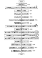
- FIG. 2 is a flowchart showing the procedure of the first embodiment of the method for manufacturing the photoelectric conversion element 10.
- the manufacturing method of the photoelectric conversion element 10 is not limited to the manufacturing method shown in each process. In each step, for example, a sputtering method, a plasma CVD method, a screen printing method, a plating method, or the like can be used as appropriate.
- an n-type single crystal silicon substrate 18 is prepared, and the light-receiving surface and the back surface of the n-type single crystal silicon substrate 18 are cleaned (S1).
- the n-type single crystal silicon substrate 18 can be cleaned using, for example, an HF aqueous solution.
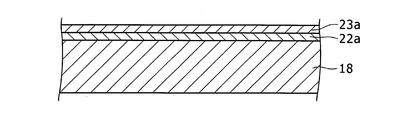
- an i-type amorphous silicon layer 22a and an n-type amorphous silicon layer 23a are formed on the back surface of the n-type single crystal silicon substrate 18 (S2).
- each of the i-type amorphous silicon layer 22a and the n-type amorphous silicon layer 23a can be formed by, for example, a plasma CVD method or the like.
- an insulating layer 24a is formed on the n-type amorphous silicon layer 23a (S3).
- the insulating layer 24a can be formed by, for example, a thin film forming method such as a sputtering method or a plasma CVD method.
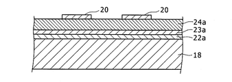
- a photoresist 20a is formed on the insulating layer 24a (S4).
- the photoresist 20a can be formed, for example, by applying a thin film with a spin coater or a slit coater.
- the unexposed photoresist 20a is excellent in alkali resistance.
- a texture structure is formed on the light receiving surface of the n-type single crystal silicon substrate 18 (S5).
- a pyramidal uneven shape is formed on the light-receiving surface of the n-type single crystal silicon substrate 18 by using an alkaline anisotropic etching solution such as a potassium hydroxide aqueous solution (KOH aqueous solution). Can be formed.
- KOH aqueous solution potassium hydroxide aqueous solution
- the photoresist 20a is exposed based on a previously prepared pattern (S6). Thereby, in the photoresist 20a, a portion irradiated with light when exposed is in a state of being dissolved in an alkaline developer.
- an alkaline developer is applied to the photoresist 20a, and the portion irradiated with light is removed from the photoresist 20a as shown in FIG. 6 (S7). Thereby, a photoresist 20 which is a mask for patterning the insulating layer 24 is formed.
- the insulating layer 24a is etched to remove a part of the insulating layer 24a, and then the photoresist 20 is peeled off (S8).
- the insulating layer 24b is formed by removing a portion of the insulating layer 24a located on a region for bonding the ip stacked portion 31 to the n-type single crystal silicon substrate 18 in a later step.
- an acidic etching solution such as an HF aqueous solution is used for the etching of the insulating layer 24a.
- each of the i-type amorphous silicon layer 16 and the n-type amorphous silicon layer 14 can be formed by, for example, a plasma CVD method or the like.
- the antireflection layer 12 is formed on the n-type amorphous silicon layer 14 (S10).
- the antireflection layer 12 can be formed, for example, by a thin film forming method such as a sputtering method or a CVD method.
- the i-type amorphous silicon layer 22a and the n-type amorphous silicon layer 23a are etched using the insulating layer 24b patterned in S8 as a mask (S11). Specifically, portions of the i-type amorphous silicon layer 22a and the n-type amorphous silicon layer 23a other than the portion covered with the insulating layer 24b are removed. Thus, the i-type amorphous silicon layer 22 and the n-type amorphous silicon layer 23 are formed by exposing a portion of the back surface of the n-type single crystal silicon substrate 18 where the insulating layer 24b is not located above. To do.
- an alkaline etching solution such as an aqueous solution containing sodium hydroxide (NaOH) is used.
- the insulating layer 24 b, the i-type amorphous silicon layer 22, the n-type amorphous silicon layer 23 and the exposed back surface of the n-type single crystal silicon substrate 18 are covered with i
- the i-type amorphous silicon layer 32a and the p-type amorphous silicon layer 33a can be formed by, for example, a plasma CVD method or the like.
- a part of the portion located on the insulating layer 24b is etched (S13). .
- the i-type amorphous silicon layer 32 and the p-type amorphous silicon layer 33 are formed.
- an alkaline etching solution such as an aqueous solution containing sodium hydroxide (NaOH) is used.
- the insulating layer 24b is etched to further remove a part of the insulating layer 24b (S14). Specifically, the insulating layer 24 is formed by removing the exposed portion of the insulating layer 24b by etching using the i-type amorphous silicon layer 32 and the p-type amorphous silicon layer 33 as a mask.
- an acidic etching solution such as an HF aqueous solution is used for the etching of the insulating layer 24b.
- a transparent conductive layer 26a and a metal layer 27a are formed (S15). Specifically, it is formed by a thin film forming method such as a plasma CVD method or a sputtering method.
- the transparent conductive layers 26 and 36 and the metal layers 27 and 37 are formed by dividing a portion of the transparent conductive layer 26 a and the metal layer 27 a located on the insulating layer 24. (S16).
- the transparent conductive layer 26a and the metal layer 27a are divided by, for example, a lithography method.
- the first electrode portion 28 and the second electrode portion 29 are sequentially formed on the metal layer 27 by electrolytic plating, and the first electrode portion 38 and the second electrode portion 29 are formed on the metal layer 37.
- Two electrode portions 39 are sequentially formed (S17). Thereby, the n-side electrode part 25 and the p-side electrode part 35 are formed.
- a texture structure is formed on the light receiving surface of the n-type single crystal silicon substrate 18 using an alkaline anisotropic etching solution such as an aqueous potassium hydroxide solution (KOH aqueous solution).
- KOH aqueous solution aqueous potassium hydroxide solution
- the substantially entire surface of the insulating layer 24b is excellent in alkali resistance. Covered with a photoresist 20a. As a result, even if a pinhole exists in the insulating layer 24b, since the pinhole is blocked by the insulating layer 24b, the alkaline anisotropic etching solution passes through the pinhole. Thus, it is possible to prevent adhesion to the i-type amorphous silicon layer 22a and the n-type amorphous silicon layer 23a. Therefore, according to the first embodiment of the method for manufacturing the photoelectric conversion element 10, the power generation characteristics of the photoelectric conversion element 10 can be improved.
- the texture structure is formed only on the light receiving surface of the n-type single crystal silicon substrate 18 and the texture structure is not formed on the back surface, the texture structure is formed only on the light receiving surface by temporarily covering the back surface with a sacrificial layer having excellent alkali resistance. After that, a separate step of peeling the sacrificial layer is required.
- the alkali resistance is excellent, and after the photoresist 20a used for patterning the insulating layer 24a is formed, Since the texture structure is formed on the light receiving surface of the n-type single crystal silicon substrate 18, a separate process such as providing a special sacrificial layer on the back surface side as described above is not necessary.
- the photoresist 20a for patterning the insulating layer 24a also serves as the sacrificial layer, the number of steps for manufacturing the photoelectric conversion element 10 can be reduced.
- FIG. 15 is a flowchart showing the procedure of the second embodiment of the method for manufacturing the photoelectric conversion element 10.
- the manufacturing method of the photoelectric conversion element 10 is not limited to the manufacturing method shown in each process. In each step, for example, a sputtering method, a plasma CVD method, a screen printing method, a plating method, or the like can be used as appropriate.
- steps of the second embodiment of the method for manufacturing the photoelectric conversion element 10 and the first embodiment of the method for manufacturing the photoelectric conversion element 10 are the same in steps S1 to S4 and S8 to S17, and between S4 to S8. Since only the process is different, the difference will be mainly described.
- S1 to S4 are performed as in the first embodiment of the method for manufacturing the photoelectric conversion element 10.
- the photoresist 20a is exposed based on a pattern prepared in advance (S5a).
- a portion irradiated with light when exposed is in a state of being dissolved in an alkaline developer.
- an alkaline developer is applied to the photoresist 20a to remove the portion irradiated with light in the photoresist 20a (S6a). Thereby, a photoresist 20 which is a mask for patterning the insulating layer 24 is formed.
- a texture structure is formed on the light receiving surface of the n-type single crystal silicon substrate 18 (S7a).
- a pyramidal uneven shape is formed on the light-receiving surface of the n-type single crystal silicon substrate 18 by using an alkaline anisotropic etching solution such as a potassium hydroxide aqueous solution (KOH aqueous solution). Can be formed.
- KOH aqueous solution potassium hydroxide aqueous solution
- S8 to S17 are performed as in the first embodiment of the method for manufacturing the photoelectric conversion element 10.
- the second embodiment of the method for manufacturing the photoelectric conversion element 10 a part of the photoresist 20a is removed before the texture structure is formed on the light receiving surface of the n-type single crystal silicon substrate 18. Therefore, it is possible to prevent damage to the i-type amorphous silicon layer 22a and the p-type amorphous silicon layer 23a located below the portion covered with the photoresist 20, but the removed portion The i-type amorphous silicon layer 22a and the p-type amorphous silicon layer 23a located below may be damaged. However, the portion that may be damaged is a region that is etched in the subsequent step S11. That is, since the portion that can be damaged is a portion that is eventually removed, the damage is not a problem. Therefore, also in the second embodiment of the method for manufacturing the photoelectric conversion element 10, the power generation characteristics of the photoelectric conversion element 10 can be improved as in the first embodiment of the method for manufacturing the photoelectric conversion element 10.
- FIG. 16 is a flowchart showing the procedure of the third embodiment of the method for manufacturing the photoelectric conversion element 10.
- the manufacturing method of the photoelectric conversion element 10 is not limited to the manufacturing method shown in each process. In each step, for example, a sputtering method, a plasma CVD method, a screen printing method, a plating method, or the like can be used as appropriate.
- steps of the third embodiment of the method for manufacturing the photoelectric conversion element 10 and the first embodiment of the method for manufacturing the photoelectric conversion element 10 are the same in steps S1 to S4 and S8 to S17, and are between S4 to S8. Since only the process is different, the difference will be mainly described.
- S1 to S4 are performed as in the first embodiment of the method for manufacturing the photoelectric conversion element 10.
- the photoresist 20a is exposed based on a pattern prepared in advance (S5b).
- a portion irradiated with light when exposed is in a state of being dissolved in an alkaline developer.
- a texture structure is formed on the light receiving surface of the n-type single crystal silicon substrate 18 using an alkaline anisotropic etching solution such as an aqueous potassium hydroxide solution (KOH aqueous solution), and the same anisotropic etching solution is used.
- the photoresist 20a is developed (S6b). As a result, a pyramidal concavo-convex shape can be formed on the light receiving surface of the n-type single crystal silicon substrate 18, and a photoresist 20 which is a mask for patterning the insulating layer 24 is formed.
- the power generation characteristics of the photoelectric conversion element 10 can be improved as in the first embodiment of the method for manufacturing the photoelectric conversion element 10.
- a part of the photoresist 20a is removed using the same alkaline anisotropic etching solution, and a texture is formed on the light receiving surface of the n-type single crystal silicon substrate 18. Forming a structure. Therefore, the number of steps of the method for manufacturing the photoelectric conversion element 10 can be reduced.
Landscapes
- Engineering & Computer Science (AREA)
- Computer Hardware Design (AREA)
- Power Engineering (AREA)
- Microelectronics & Electronic Packaging (AREA)
- Physics & Mathematics (AREA)
- Condensed Matter Physics & Semiconductors (AREA)
- Electromagnetism (AREA)
- General Physics & Mathematics (AREA)
- Life Sciences & Earth Sciences (AREA)
- Sustainable Energy (AREA)
- Sustainable Development (AREA)
- Chemical & Material Sciences (AREA)
- Crystallography & Structural Chemistry (AREA)
- Manufacturing & Machinery (AREA)
- Photovoltaic Devices (AREA)
Abstract
La présente invention concerne un procédé de fabrication d'un élément de conversion photoélectrique (10). Selon ce procédé, une partie de couche semi-conductrice amorphe est formée sur la surface arrière d'un substrat de silicium monocristallin de type n (18), une couche isolante (24a) est formée sur la partie de couche semi-conductrice amorphe, une résine photosensible (20a) est déposée sur la couche isolante (24a), et la surface recevant la lumière sur le côté du substrat de silicium monocristallin de type n (18) à l'opposé de la surface arrière est gravée alors que la résine photosensible (20a) recouvre la couche isolante (24a).
Applications Claiming Priority (2)
| Application Number | Priority Date | Filing Date | Title |
|---|---|---|---|
| JP2011-068126 | 2011-03-25 | ||
| JP2011068126 | 2011-03-25 |
Publications (1)
| Publication Number | Publication Date |
|---|---|
| WO2012132616A1 true WO2012132616A1 (fr) | 2012-10-04 |
Family
ID=46930378
Family Applications (1)
| Application Number | Title | Priority Date | Filing Date |
|---|---|---|---|
| PCT/JP2012/053851 WO2012132616A1 (fr) | 2011-03-25 | 2012-02-17 | Procédé de fabrication d'un élément de conversion photoélectrique |
Country Status (1)
| Country | Link |
|---|---|
| WO (1) | WO2012132616A1 (fr) |
Cited By (1)
| Publication number | Priority date | Publication date | Assignee | Title |
|---|---|---|---|---|
| WO2016147565A1 (fr) * | 2015-03-16 | 2016-09-22 | パナソニックIpマネジメント株式会社 | Cellule de batterie solaire |
Citations (2)
| Publication number | Priority date | Publication date | Assignee | Title |
|---|---|---|---|---|
| JP2010504636A (ja) * | 2006-09-26 | 2010-02-12 | コミサリア、ア、レネルジ、アトミク | 背面ヘテロ接合太陽電池製造方法 |
| WO2010113750A1 (fr) * | 2009-03-30 | 2010-10-07 | 三洋電機株式会社 | Pile solaire |
-
2012
- 2012-02-17 WO PCT/JP2012/053851 patent/WO2012132616A1/fr active Application Filing
Patent Citations (2)
| Publication number | Priority date | Publication date | Assignee | Title |
|---|---|---|---|---|
| JP2010504636A (ja) * | 2006-09-26 | 2010-02-12 | コミサリア、ア、レネルジ、アトミク | 背面ヘテロ接合太陽電池製造方法 |
| WO2010113750A1 (fr) * | 2009-03-30 | 2010-10-07 | 三洋電機株式会社 | Pile solaire |
Cited By (2)
| Publication number | Priority date | Publication date | Assignee | Title |
|---|---|---|---|---|
| WO2016147565A1 (fr) * | 2015-03-16 | 2016-09-22 | パナソニックIpマネジメント株式会社 | Cellule de batterie solaire |
| JPWO2016147565A1 (ja) * | 2015-03-16 | 2017-12-07 | パナソニックIpマネジメント株式会社 | 太陽電池セル |
Similar Documents
| Publication | Publication Date | Title |
|---|---|---|
| JP5891382B2 (ja) | 光電変換素子の製造方法 | |
| JP5705968B2 (ja) | 光電変換装置及びその製造方法 | |
| KR101863294B1 (ko) | 태양전지 및 그 제조 방법 | |
| US9006564B2 (en) | Method of manufacturing solar cell and solar cell | |
| JP6817764B2 (ja) | 太陽電池セル、及び太陽電池セルの製造方法 | |
| WO2012132655A1 (fr) | Élément de conversion photoélectrique à jonction arrière et son procédé de fabrication | |
| JP2013219065A (ja) | 太陽電池及び太陽電池の製造方法 | |
| JP6677801B2 (ja) | 結晶シリコン系太陽電池およびその製造方法、ならびに太陽電池モジュール | |
| JP2013120863A (ja) | 太陽電池の製造方法 | |
| JPWO2010064549A1 (ja) | 薄膜光電変換装置の製造方法 | |
| US20140024168A1 (en) | Method for producing photoelectric conversion device | |
| JP2013131586A (ja) | 裏面電極型太陽電池の製造方法 | |
| TWI587540B (zh) | 太陽能電池透明導電膜上實施電鍍製程的方法 | |
| JP5820989B2 (ja) | 光電変換素子の製造方法 | |
| JP2014072209A (ja) | 光電変換素子および光電変換素子の製造方法 | |
| WO2012132616A1 (fr) | Procédé de fabrication d'un élément de conversion photoélectrique | |
| EP3576160A1 (fr) | Cellule solaire et son procédé de préparation | |
| WO2012132613A1 (fr) | Procédé de fabrication d'un élément de conversion photoélectrique | |
| JP2013168605A (ja) | 太陽電池の製造方法 | |
| JP2014183073A (ja) | 光電変換素子および光電変換素子の製造方法 | |
| JP7146786B2 (ja) | 太陽電池の製造方法、太陽電池および太陽電池モジュール | |
| WO2020149128A1 (fr) | Procédé de production de cellules solaires | |
| WO2017203751A1 (fr) | Cellule solaire et son procédé de fabrication, et panneau solaire | |
| WO2012132064A1 (fr) | Élément photovoltaïque | |
| JPWO2015145886A1 (ja) | 電極パターンの形成方法及び太陽電池の製造方法 |
Legal Events
| Date | Code | Title | Description |
|---|---|---|---|
| 121 | Ep: the epo has been informed by wipo that ep was designated in this application |
Ref document number: 12763538 Country of ref document: EP Kind code of ref document: A1 |
|
| NENP | Non-entry into the national phase |
Ref country code: DE |
|
| 122 | Ep: pct application non-entry in european phase |
Ref document number: 12763538 Country of ref document: EP Kind code of ref document: A1 |
|
| NENP | Non-entry into the national phase |
Ref country code: JP |