WO2012132019A1 - 三次元実装半導体装置及びその製造方法 - Google Patents
三次元実装半導体装置及びその製造方法 Download PDFInfo
- Publication number
- WO2012132019A1 WO2012132019A1 PCT/JP2011/058361 JP2011058361W WO2012132019A1 WO 2012132019 A1 WO2012132019 A1 WO 2012132019A1 JP 2011058361 W JP2011058361 W JP 2011058361W WO 2012132019 A1 WO2012132019 A1 WO 2012132019A1
- Authority
- WO
- WIPO (PCT)
- Prior art keywords
- semiconductor device
- substrate
- dimensional mounting
- mounting semiconductor
- silicon
- Prior art date
Links
Images


Classifications
-
- H—ELECTRICITY
- H01—ELECTRIC ELEMENTS
- H01L—SEMICONDUCTOR DEVICES NOT COVERED BY CLASS H10
- H01L23/00—Details of semiconductor or other solid state devices
- H01L23/34—Arrangements for cooling, heating, ventilating or temperature compensation ; Temperature sensing arrangements
- H01L23/46—Arrangements for cooling, heating, ventilating or temperature compensation ; Temperature sensing arrangements involving the transfer of heat by flowing fluids
- H01L23/473—Arrangements for cooling, heating, ventilating or temperature compensation ; Temperature sensing arrangements involving the transfer of heat by flowing fluids by flowing liquids
-
- H—ELECTRICITY
- H01—ELECTRIC ELEMENTS
- H01L—SEMICONDUCTOR DEVICES NOT COVERED BY CLASS H10
- H01L25/00—Assemblies consisting of a plurality of individual semiconductor or other solid state devices ; Multistep manufacturing processes thereof
- H01L25/03—Assemblies consisting of a plurality of individual semiconductor or other solid state devices ; Multistep manufacturing processes thereof all the devices being of a type provided for in the same subgroup of groups H01L27/00 - H01L33/00, or in a single subclass of H10K, H10N, e.g. assemblies of rectifier diodes
- H01L25/04—Assemblies consisting of a plurality of individual semiconductor or other solid state devices ; Multistep manufacturing processes thereof all the devices being of a type provided for in the same subgroup of groups H01L27/00 - H01L33/00, or in a single subclass of H10K, H10N, e.g. assemblies of rectifier diodes the devices not having separate containers
- H01L25/065—Assemblies consisting of a plurality of individual semiconductor or other solid state devices ; Multistep manufacturing processes thereof all the devices being of a type provided for in the same subgroup of groups H01L27/00 - H01L33/00, or in a single subclass of H10K, H10N, e.g. assemblies of rectifier diodes the devices not having separate containers the devices being of a type provided for in group H01L27/00
- H01L25/0652—Assemblies consisting of a plurality of individual semiconductor or other solid state devices ; Multistep manufacturing processes thereof all the devices being of a type provided for in the same subgroup of groups H01L27/00 - H01L33/00, or in a single subclass of H10K, H10N, e.g. assemblies of rectifier diodes the devices not having separate containers the devices being of a type provided for in group H01L27/00 the devices being arranged next and on each other, i.e. mixed assemblies
-
- H—ELECTRICITY
- H01—ELECTRIC ELEMENTS
- H01L—SEMICONDUCTOR DEVICES NOT COVERED BY CLASS H10
- H01L25/00—Assemblies consisting of a plurality of individual semiconductor or other solid state devices ; Multistep manufacturing processes thereof
- H01L25/50—Multistep manufacturing processes of assemblies consisting of devices, each device being of a type provided for in group H01L27/00 or H01L29/00
-
- H—ELECTRICITY
- H01—ELECTRIC ELEMENTS
- H01L—SEMICONDUCTOR DEVICES NOT COVERED BY CLASS H10
- H01L2225/00—Details relating to assemblies covered by the group H01L25/00 but not provided for in its subgroups
- H01L2225/03—All the devices being of a type provided for in the same subgroup of groups H01L27/00 - H01L33/648 and H10K99/00
- H01L2225/04—All the devices being of a type provided for in the same subgroup of groups H01L27/00 - H01L33/648 and H10K99/00 the devices not having separate containers
- H01L2225/065—All the devices being of a type provided for in the same subgroup of groups H01L27/00 - H01L33/648 and H10K99/00 the devices not having separate containers the devices being of a type provided for in group H01L27/00
- H01L2225/06503—Stacked arrangements of devices
- H01L2225/06551—Conductive connections on the side of the device
-
- H—ELECTRICITY
- H01—ELECTRIC ELEMENTS
- H01L—SEMICONDUCTOR DEVICES NOT COVERED BY CLASS H10
- H01L2225/00—Details relating to assemblies covered by the group H01L25/00 but not provided for in its subgroups
- H01L2225/03—All the devices being of a type provided for in the same subgroup of groups H01L27/00 - H01L33/648 and H10K99/00
- H01L2225/04—All the devices being of a type provided for in the same subgroup of groups H01L27/00 - H01L33/648 and H10K99/00 the devices not having separate containers
- H01L2225/065—All the devices being of a type provided for in the same subgroup of groups H01L27/00 - H01L33/648 and H10K99/00 the devices not having separate containers the devices being of a type provided for in group H01L27/00
- H01L2225/06503—Stacked arrangements of devices
- H01L2225/06589—Thermal management, e.g. cooling
-
- H—ELECTRICITY
- H01—ELECTRIC ELEMENTS
- H01L—SEMICONDUCTOR DEVICES NOT COVERED BY CLASS H10
- H01L25/00—Assemblies consisting of a plurality of individual semiconductor or other solid state devices ; Multistep manufacturing processes thereof
- H01L25/03—Assemblies consisting of a plurality of individual semiconductor or other solid state devices ; Multistep manufacturing processes thereof all the devices being of a type provided for in the same subgroup of groups H01L27/00 - H01L33/00, or in a single subclass of H10K, H10N, e.g. assemblies of rectifier diodes
- H01L25/04—Assemblies consisting of a plurality of individual semiconductor or other solid state devices ; Multistep manufacturing processes thereof all the devices being of a type provided for in the same subgroup of groups H01L27/00 - H01L33/00, or in a single subclass of H10K, H10N, e.g. assemblies of rectifier diodes the devices not having separate containers
- H01L25/065—Assemblies consisting of a plurality of individual semiconductor or other solid state devices ; Multistep manufacturing processes thereof all the devices being of a type provided for in the same subgroup of groups H01L27/00 - H01L33/00, or in a single subclass of H10K, H10N, e.g. assemblies of rectifier diodes the devices not having separate containers the devices being of a type provided for in group H01L27/00
- H01L25/0657—Stacked arrangements of devices
-
- H—ELECTRICITY
- H01—ELECTRIC ELEMENTS
- H01L—SEMICONDUCTOR DEVICES NOT COVERED BY CLASS H10
- H01L2924/00—Indexing scheme for arrangements or methods for connecting or disconnecting semiconductor or solid-state bodies as covered by H01L24/00
- H01L2924/0001—Technical content checked by a classifier
- H01L2924/0002—Not covered by any one of groups H01L24/00, H01L24/00 and H01L2224/00
Definitions
- the present invention relates to a three-dimensional mounting semiconductor device in which a plurality of semiconductor chips are stacked and mounted, and a method for manufacturing the same.
- a cooling technique using a microchannel has attracted attention as a candidate technique for efficiently cooling each semiconductor chip of a three-dimensional mounting semiconductor device.
- This technique is a method of cooling each semiconductor chip by providing a plurality of microchannels in a three-dimensional mounting semiconductor device and flowing a cooling liquid through the microchannels.
- a microchannel is a flow path for liquid having a micro-order dimension.
- the microscale flow is a laminar flow and has an effect that the influence of the surface force (fluid viscosity effect) is larger than that of the body force. Therefore, the heat transfer rate can be improved with a small flow rate of fluid. As a result, the heat generated from the heat source can be efficiently transferred and the necessary cooling performance can be obtained. Furthermore, since the width and height of the channel are on the micro order, there is an advantage that the cooling device can be miniaturized. In addition, since the amount of fluid used is small, there is an advantage that the degree of freedom in designing the fluid movement area and storage area is improved.
- An object of the present invention relates to a three-dimensional mounting semiconductor device having a microchannel, and to provide a three-dimensional mounting semiconductor device capable of improving the reliability of a joint portion between semiconductor chips and other members and a method for manufacturing the same. It is in.
- a plurality of first substrates on which groove-shaped recesses are formed and a plurality of second substrates on which semiconductor elements are formed are alternately stacked, and the first substrate Unevenness due to the difference in size between the substrate and the second substrate is formed on the side surface, and a first through hole defined by the inner surface of the groove-shaped recess and the surface of the first substrate is formed.
- a laminated structure and a third substrate bonded to the side surface of the laminated structure, and having a concavo-convex formed on the joint surface with the laminated structure and fitted to the concavo-convex of the side surface of the laminated structure.
- a three-dimensional mounting semiconductor device is provided.
- a plurality of first substrates on which groove-like recesses are formed and a plurality of second substrates on which semiconductor elements are formed are alternately stacked, and the groove-like The first through hole defined by the inner surface of the recess and the surface of the first substrate is formed, and the unevenness due to the difference in size between the first substrate and the second substrate is formed on the side surface.
- a method for manufacturing a three-dimensional mounting semiconductor device comprising: a step of forming a stacked structure, and a step of bonding a third substrate having protrusions and recesses fitted to the protrusions and recesses of the side surfaces to the side surface of the stacked structure.
- the reliability of the joint portion between the semiconductor chips and other members can be improved.
- the reliability and cooling efficiency of the three-dimensional mounting semiconductor device can be improved.
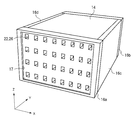
- FIG. 1 is a perspective view showing the structure of the three-dimensional mounting semiconductor device according to the first embodiment.
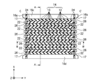
- FIG. 2 is a cross-sectional view (part 1) showing the structure of the three-dimensional mounting semiconductor device according to the first embodiment.
- FIG. 3 is a sectional view (No. 2) showing the structure of the three-dimensional mounting semiconductor device according to the first embodiment.
- FIG. 4 is a cross-sectional view (part 3) illustrating the structure of the three-dimensionally mounted semiconductor device according to the first embodiment.
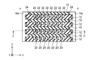
- FIG. 5 is a plan view (part 1) showing the structure of a silicon chip used in the three-dimensionally mounted semiconductor device according to the first embodiment.
- FIG. 6 is a plan view (part 2) illustrating the structure of the silicon chip used in the three-dimensionally mounted semiconductor device according to the first embodiment.
- FIG. 1 is a perspective view showing the structure of the three-dimensional mounting semiconductor device according to the first embodiment.
- FIG. 2 is a cross-sectional view (part 1) showing the structure of the three-dimensional mounting semiconductor device
- FIG. 7 is a cross-sectional view showing a structure in which piping is joined to the three-dimensional mounting semiconductor device according to the first embodiment.
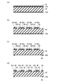
- FIG. 8 is a process cross-sectional view (part 1) illustrating the method for manufacturing the three-dimensionally mounted semiconductor device according to the first embodiment.
- FIG. 9 is a process cross-sectional view (part 2) illustrating the method for manufacturing the three-dimensionally mounted semiconductor device according to the first embodiment.
- FIG. 10 is a process cross-sectional view (part 3) illustrating the method for manufacturing the three-dimensionally mounted semiconductor device according to the first embodiment.
- FIG. 11 is a process cross-sectional view (part 4) illustrating the method for manufacturing the three-dimensionally mounted semiconductor device according to the first embodiment.
- FIG. 12 is a perspective view showing the structure of the three-dimensional mounting semiconductor device according to the second embodiment.
- FIG. 13 is a cross-sectional view showing the structure of the three-dimensional mounting semiconductor device according to the second embodiment.
- FIG. 14 is a plan view showing the structure of a silicon chip used in the three-dimensional mounting semiconductor device according to the second embodiment.
- FIG. 15 is a process cross-sectional view (part 1) illustrating the method for manufacturing the three-dimensionally mounted semiconductor device according to the second embodiment.
- FIG. 16 is a process cross-sectional view (part 2) illustrating the method for manufacturing the three-dimensionally mounted semiconductor device according to the second embodiment.
- FIG. 17 is a cross-sectional view showing the structure of the three-dimensionally mounted semiconductor device according to the third embodiment.
- FIG. 18 is a process cross-sectional view illustrating the method of manufacturing the three-dimensionally mounted semiconductor device according to the third embodiment.
- FIG. 1 is a perspective view showing the structure of the three-dimensional mounting semiconductor device according to the present embodiment.
- 2 to 4 are sectional views showing the structure of the three-dimensional mounting semiconductor device according to the present embodiment.
- 5 and 6 are plan views showing the structure of the silicon chip used in the three-dimensional mounting semiconductor device according to the present embodiment.
- FIG. 7 is a cross-sectional view showing a structure in which piping is joined to the three-dimensional mounting semiconductor device according to the present embodiment.
- 8 to 11 are process cross-sectional views illustrating the method of manufacturing the three-dimensionally mounted semiconductor device according to the present embodiment.
- FIGS. 2 is a cross-sectional view in a direction parallel to the XZ plane of FIG. 1, and corresponds to a cross-sectional view taken along the line AA ′ of FIG. 3 is a cross-sectional view in a direction parallel to the YZ plane of FIG. 1, and corresponds to a cross-sectional view taken along the line BB ′ of FIG. 4 is a cross-sectional view in a direction parallel to the XY plane of FIG. 1, and corresponds to a cross section taken along the line CC ′ of FIG.
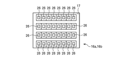
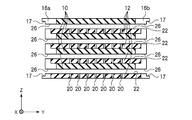
- the three-dimensionally mounted semiconductor device includes a stacked structure 14 and silicon chips 16 a, 16 b, 16 c, and 16 d bonded to the respective side surfaces of the stacked structure 14. .
- a plurality of microchannels 22 and 26 penetrating between the side surface on which the silicon chip 16a is formed and the side surface on which the silicon chip 16b is formed are formed.
- the laminated structure 14 is formed by alternately stacking semiconductor chips 10 and microchannel chips 12.
- semiconductor chips 10 and microchannel chips 12 are alternately stacked.
- the number of semiconductor chips 10 and microchannel chips 12 is limited to these. It is not a thing.
- the semiconductor chip 10 is formed by forming a semiconductor element having a predetermined function on a silicon substrate, and has through wiring (not shown) as necessary.
- the microchannel chip 12 is a plate-like body formed of silicon, and has a through wiring 20 formed so as to penetrate in the Z direction and a groove (microchannel 22) extending in the Y direction.
- the groove formed in the microchannel chip 12 is covered with the semiconductor chip 10.
- a plurality of microchannels 22 penetrating the laminated structure 14 in the Y direction are formed between the semiconductor chip 10 and the microchannel chip 12.
- the microchannel 22 is a channel (groove) for flowing a cooling fluid such as water. By flowing a cooling fluid through the microchannel 22, the semiconductor chip 10 that has generated heat due to the operation can be cooled.
- the microchannel 22 has a size of about 70 ⁇ m in width and about 100 ⁇ m in height, for example.
- connection wiring is formed between the upper and lower semiconductor chips 10 sandwiching the microchannel chip 12 by the through wiring 20 formed in the microchannel chip 12.
- the size of the microchannel chip 12 in the X direction and the Y direction is larger than the size of the semiconductor chip 10 in the X direction and the Y direction.
- the size (thickness) in the Z direction of the semiconductor chip 10 and the size (thickness) in the Z direction of the microchannel chip 12 are not particularly limited.
- the size (thickness) in the Z direction of the semiconductor chip 10 is appropriately selected from about 50 ⁇ m to 1000 ⁇ m depending on, for example, the size of the semiconductor chip 10 in the X and Y directions and the method of forming the semiconductor chip 10.
- the size (thickness) in the Z direction of the microchannel chip 12 is appropriately selected from about 50 ⁇ m to 1000 ⁇ m depending on, for example, the size of the microchannel chip 12 in the X and Y directions and the forming method of the microchannel chip 12. .
- the size of the semiconductor chip 10 is not particularly limited, but the size in the X direction is 10,000 ⁇ m, the size in the Y direction is 10,000 ⁇ m, and the size (thickness) in the Z direction is 500 ⁇ m.
- the size of the microchannel chip 12 is not particularly limited, but the size in the X direction is 10200 ⁇ m, the size in the Y direction is 10200 ⁇ m, and the size (thickness) in the Z direction is 200 ⁇ m.
- the size of the semiconductor chip 10 in the X direction and the Y direction may be different from the size of the microchannel chip 12 in the X direction and the Y direction. You may make it make it smaller than the size of 10 X directions and Y directions.
- the size of the semiconductor chip 10 may be increased in one of the X direction and the Y direction, and the size of the microchannel chip 12 may be increased in the other of the X direction and the Y direction.
- a step corresponding to the size difference between the semiconductor chip 10 and the microchannel chip 12 is formed on each side surface of the stacked structure 14. (See FIGS. 2 and 3).
- the semiconductor chip 10 and the microchannel chip 12 are preferably formed of materials having the same thermal expansion coefficient. If the thermal expansion coefficient of the material forming the semiconductor chip 10 and the thermal expansion coefficient of the material forming the microchannel chip 12 are different, the heat between the semiconductor chip 10 and the microchannel chip 12 is driven by the heat generated when the semiconductor chip 10 is driven. This is because there is a risk of cracking.
- the semiconductor chip 10 and the microchannel chip 12 are formed of silicon of the same material, but the same material is not necessarily used as long as the materials have similar thermal expansion coefficients.
- the silicon chips 16a, 16b, 16c, and 16c are bonded to the four side surfaces of the laminated structure 14, respectively, as shown in FIGS.
- the silicon chip 16a and the silicon chip 16b are respectively formed on two side surfaces of the multilayer structure 14 intersecting with the Y direction, and the silicon chip 16c and the silicon chip 16d are two of the multilayer structure 14 intersecting with the X direction. Each is formed on the side.
- the silicon chip 16a has a structure shown in FIGS. 5 (a) and 5 (b).
- irregularities 25 and through holes 26 are formed on the surface of the silicon chip 16a to be bonded to the laminated structure 14.
- the unevenness 25 has a shape that fits into the step on the side surface of the laminated structure 14.
- the through hole 26 has the same size as the microchannel 22 and is formed so as to coincide with the position of the microchannel 22 exposed on the side surface of the laminated structure 14.
- a recess 17 and a through hole 26 are formed on the surface of the silicon chip 16a opposite to the surface to be bonded to the laminated structure 14.
- the concave portion 17 is provided for convenience when connecting to a pipe (not shown) for introducing a cooling fluid to be passed through the microchannel 22.
- the size of the recess 17 is not particularly limited.
- the size in the Y direction is 500 ⁇ m
- the size in the Z direction is 2800 ⁇ m, for example.
- the other surface of the silicon chip 16a is not particularly limited, but is a flat surface.
- the silicon chip 16b has the same shape as the silicon chip 16a.
- the silicon chip 16 c has an uneven surface 27 having a shape that fits into a step on the side surface of the laminated structure 14 on the surface to be joined to the laminated structure 14.
- the other surface of the silicon chip 16c is not particularly limited, it is a flat surface.
- the silicon chip 16d has the same shape as the silicon chip 16c.
- the silicon chips 16a, 16b, 16c, and 16d are joined to the respective side surfaces of the laminated structure 14 via the silicone rubber layer 24 as shown in FIGS.
- the thickness of the silicone rubber layer 24 is not specifically limited, For example, it is about 10 micrometers.
- the silicon chips 16a, 16b, 16c, and 16d are formed of a material having the same thermal expansion coefficient as that of the material forming the laminated structure 14. If the thermal expansion coefficient of the material forming the silicon chips 16a, 16b, 16c, and 16d is different from the thermal expansion coefficient of the material forming the stacked structure 14, the stacked structure 14 and silicon are heated by the heat generated when the semiconductor chip 10 is driven. This is because cracks may occur between the chips 16a, 16b, 16c, and 16d. In the above example, silicon is formed of the same material as that of the laminated structure 14, but it is not always necessary to use the same material as long as it has a similar thermal expansion coefficient.
- FIG. 7A is a cross-sectional view in a direction parallel to the XY plane
- FIG. 7B is a cross-sectional view in a direction parallel to the YZ plane.
- piping for flowing the cooling fluid is provided on the surface on the silicon chip 16a side and the surface on the silicon chip 16b side of the three-dimensional mounting semiconductor device according to the present embodiment. Connected. That is, the pipe 60a is connected to the surface on the silicon chip 16a side. A pipe 60b is connected to the surface on the silicon chip 16b side.
- the pipes 60 a and 60 b are joined to the concave portion 17 of the silicon chips 16 a and 16 b through the micro O-ring 62.
- the diameters of the pipes 60a and 60b are appropriately selected according to the opening dimensions of the recesses 17 of the silicon chips 16a and 16b.
- the size of the recess 17 of the silicon chips 16a and 16b is desirably selected as appropriate according to the size of the diameter of the pipes 60a and 60b.
- the shape of the recess 17 is not limited to a rectangular shape, and can be appropriately selected according to the shapes of the pipes 60a and 60b.
- the pipe 60a and the pipe 60b are connected by the jig 64, and the three-dimensional mounting semiconductor device is sandwiched between the pipe 60a and the pipe 60b, thereby joining the pipe 60a and the silicon chip 16a and the pipe 60b and the silicon chip 16b.
- the semiconductor chip 10 and the microchannel chip 12 for forming the laminated structure 14 are prepared.
- the sizes of the microchannel chip 12 in the X direction and the Y direction are different from the sizes of the semiconductor chip 10 in the X direction and the Y direction.
- the size of the semiconductor chip 10 in the X direction is 10000 ⁇ m
- the size in the Y direction is 10000 ⁇ m
- the size (thickness) in the Z direction is 500 ⁇ m
- the size of the microchannel chip 12 in the X direction is 10200 ⁇ m
- the size in the Y direction is 10200 ⁇ m
- the size (thickness) in the Z direction is 200 ⁇ m.
- the prepared semiconductor chips 10 and microchannel chips 12 are alternately stacked to form a laminated structure 14.
- the method for forming the laminated structure 14 is not particularly limited, and for example, a surface activated bonding method can be used.
- the surface activated bonding method is a method of performing pressure activation bonding by performing alignment between wirings after irradiating an ion beam to a bonding surface to perform surface activation.
- a silicon oxide or silicon oxide film surface on the bonding surface may be subjected to a hydrophilic treatment, and an oxide film direct bonding method in which bonding is performed with a hydroxyl group may be used.
- a metal bonding method may be used in which a thin film such as a Cu film or an Al film is formed on the bonding surface and bonded using diffusion of metal atoms.
- a resin joining method joined using BCB Benzocyclobutene, benzocyclobutene
- silicon chips 16a, 16b, 16c, and 16d are manufactured separately from the laminated structure 14.
- the silicon chips 16a and 16b are manufactured as follows, for example.
- a silicon substrate 40 is prepared as a substrate for forming the silicon chips 16a and 16b.
- the thickness of the silicon substrate 40 is not particularly limited, but is about 200 ⁇ m to 525 ⁇ m, for example, 500 ⁇ m.
- a pattern such as a photoresist is formed on the front and back surfaces of the substrate and etching is performed, it is desirable to use a silicon substrate 40 in which both surfaces of the substrate are mirror-polished.
- the silicon substrate 40 may be provided with conductivity by doping impurities.
- silicon oxide films 42a and 42b are formed on the front and back surfaces of the silicon substrate 40 by, eg, plasma CVD.
- the film thickness of the silicon oxide films 42a and 42b is, for example, about 1 to 2 ⁇ m.
- a photoresist film 43 is formed on the silicon oxide film 42a by, eg, spin coating.
- the thickness of the photoresist film 43 is about 4 ⁇ m, for example.
- a photoresist (trade name: AZ P4620) manufactured by AZ Electronic Materials is used.
- the photoresist is applied on the silicon oxide film 42a at a rotational speed of 2000 rpm, for example. Thereafter, the photoresist is heat-treated at 120 ° C.
- a photoresist film 43 is formed on the silicon oxide film 42a (FIG. 8A).
- the photoresist film 43 is patterned by a photolithography technique, and an opening 44 is formed in the formation region of the through hole 26 of the photoresist film 43.
- the opening size of the opening 44 is, for example, about 70 ⁇ m ⁇ 100 ⁇ m.
- the silicon oxide film 42a is etched by wet etching using, for example, buffered hydrofluoric acid. As a result, an opening 45 is formed in the through-hole 26 formation region of the silicon oxide film 42a (FIG. 8B).
- the etching time is appropriately adjusted according to the thickness of the silicon oxide film 42a.
- the back surface of the silicon substrate 40 is covered with a protective film such as a photoresist film so that the silicon oxide film 42b on the back surface is not etched when the silicon oxide film 42a is etched.
- the photoresist film 43 is removed by, for example, ashing.
- the silicon oxide film 42b formed on the back surface of the silicon substrate 40 is patterned to form an opening 46 in a region where the recess 17 of the silicon oxide film 42b is to be formed.
- the opening size of the opening 46 is, for example, 10000 ⁇ m ⁇ 2000 ⁇ m (FIG. 8C).
- a photoresist film 48 is formed on the silicon oxide film 42a by, eg, spin coating.
- the film thickness of the photoresist film 48 is, eg, about 4 ⁇ m.
- the photoresist film 48 is patterned by a photolithography technique. Thereby, an opening 50 corresponding to the convex portion of the unevenness 25 is formed in the photoresist film 48 (FIG. 8D).
- the opening size of the opening 50 is, for example, about 10200 ⁇ m ⁇ 200 ⁇ m.
- the silicon substrate 40 is etched by about 300 ⁇ m, for example, by DRIE (DeepRIReactive Ion Etching) method (FIG. 9A).
- DRIE DeepRIReactive Ion Etching
- DRIE is an etching technique that repeats etching and etching sidewall protection.
- etching is performed using SF 6 gas.
- side wall protection step the side wall is protected using, for example, C 4 F 8 gas. It becomes anisotropic etching in which lateral etching is suppressed by the protective film. Thereby, a groove with a high aspect ratio can be formed.
- C 4 F 8 gas is introduced at a flow rate of 130 sccm, for example, under a condition where the coil power is 600 W and the pressure in the process chamber is 14.5 mTorr 6.3 seconds. Can be applied.
- the flow rate of SF 6 gas is 130 sccm under the condition that the coil power is 600 W, the pressure in the process chamber is 14.5 mTorr, the RF power to the substrate is 23 W at 380 kHz. It is possible to apply the process of 7.5 seconds introduced in the above. The first step and the second step are repeated alternately.
- the silicon oxide film 42a is etched by dry etching, for example (FIG. 9B).
- the silicon substrate 40 is etched by, for example, about 100 ⁇ m by, for example, DRIE (FIG. 9C).
- DRIE DRIE
- the same conditions as those described above with reference to FIG. 7B can be applied.
- the photoresist film 48 is removed by, for example, ashing, and the silicon oxide film 42a is removed by, for example, dry etching.
- the support substrate 52 is bonded onto the silicon substrate 40.
- a heat release sheet (trade name: Riva Alpha 3195M) manufactured by Nitto Denko Corporation is used.
- the thickness of the support substrate is, for example, 525 ⁇ m.
- the support substrate 52 is used to prevent damage to the silicon substrate 40 in a process of etching the silicon substrate 40 described later from the back surface.
- the silicon substrate 40 is etched by, for example, 100 ⁇ m from the back side of the silicon substrate 40 by, for example, DRIE. Thereby, the concave portion 17 is formed on the back surface side of the silicon substrate 40. Further, the concave portion 17 formed on the back surface side of the silicon substrate 40 and the opening formed on the front surface side of the silicon substrate 40 are connected to form a through hole 26 (FIG. 9D).
- the etching conditions the same conditions as those described above with reference to FIG. 7B can be applied.
- the support substrate 52 is peeled off.
- the silicon oxide film 42b is removed by, for example, dry etching (FIG. 9E).
- the silicon chip 16a and the silicon chip 16b are manufactured.
- the silicon chips 16c and 16d are manufactured as follows, for example.
- a silicon substrate 54 is prepared as a substrate for forming the silicon chips 16c and 16d.
- the thickness of the silicon substrate 54 is not particularly limited, but is about 200 ⁇ m to 525 ⁇ m, for example, 500 ⁇ m.
- a pattern such as a photoresist is formed on the surface of the substrate and etching is performed, it is desirable to use a silicon substrate 54 whose surface is mirror-polished.
- the silicon substrate 54 may be provided with conductivity by doping impurities.
- a photoresist film 56 is formed on the silicon substrate 54 by, eg, spin coating.
- the thickness of the photoresist film 56 is, for example, about 4 ⁇ m (FIG. 10A).
- the photoresist film 56 is patterned by a photolithography technique, and openings 58 corresponding to the convex portions of the irregularities 27 are formed in the photoresist film 56.
- the opening size of the opening 58 is, for example, about 10200 ⁇ m ⁇ 200 ⁇ m.
- the silicon substrate 56 is etched by, for example, DRIE, for example, by about 100 ⁇ m (FIG. 10C). As a result, the concave portion of the unevenness 27 is formed in the silicon substrate 56.
- the etching conditions the same conditions as those described above with reference to FIG. 7B can be applied.
- the photoresist film 56 is removed by, for example, ashing.
- the silicon chips 16c and 16d are manufactured.
- the laminated structure 14 and the silicon chips 16a, 16b, 16c, and 16d are joined.
- PDMS polydimethylsilioxane
- the silicone rubber layer 24 is formed on the uneven surfaces of the silicon chips 16a and 16b (FIG. 11A).
- the thickness of the silicone rubber layer 24 is, for example, about 10 ⁇ m.
- the side surface of the laminated structure 14 is irradiated with excimer light.
- Excimer light is laser light using a mixed gas such as a rare gas or halogen.
- the surface of the laminated structure 14, that is, the silicon atoms that are the forming materials of the semiconductor chip 10 and the microchannel chip 12 are activated.
- the side surface of the activated laminated structure 14 and the surfaces of the silicon chips 16a and 16b on which the silicone rubber layer 24 is formed are pressure-bonded.
- the silicon chips 16a and 16b and the laminated structure 14 are joined via the silicone rubber layer 24 (FIG. 11B).
- forming the silicone rubber layer 24 on the bonding surface also has an effect of absorbing an impact when the silicon chips 16a, 16b, 16c, and 16d and the laminated structure 14 are bonded.
- the unevenness 25 on the surface of the silicon chips 16a and 16b and the step on the side surface of the laminated structure 14 are fitted, the unevenness 25 and the microchannel 22 are aligned in advance so that the position of the through hole 26 and the position of the microchannel 22 match.
- the alignment of the through hole 26 and the microchannel 22 becomes unnecessary.
- the three-dimensional mounting semiconductor device according to the present embodiment is manufactured.
- the semiconductor chip 10, the microchannel chip 12, and the silicon chips 16a, 16b, 16c, and 16d are made of silicon. Therefore, high reliability with respect to thermal expansion can be ensured.
- a step is provided on the side surface of the multilayer structure 14, and irregularities corresponding to the step on the side surface of the multilayer structure 14 are formed on the silicon chips 16a to 16d. Bonding with the chips 16a to 16d can be easily performed.
- the silicon chips 16a and 16b and the pipes 60a and 60b can be easily joined by the concave portions 17 formed in the silicon chips 16a and 16b.
- the order of the process of mounting the three-dimensional mounting semiconductor device on another substrate can be selected more flexibly. More specifically, after bonding the silicon chips 16a and 16b and the pipes 60a and 60b, the three-dimensional mounting semiconductor device may be mounted on another substrate. Alternatively, the silicon chips 16a and 16b and the pipes 60a and 60b may be joined after the three-dimensional mounting semiconductor device is mounted on another substrate.
- FIGS. 1 to 11 A three-dimensional mounting semiconductor device and a manufacturing method thereof according to the second embodiment will be described with reference to FIGS.
- the same components as those of the three-dimensional mounting semiconductor device according to the first embodiment shown in FIGS. 1 to 11 are denoted by the same reference numerals, and description thereof is omitted or simplified.
- FIG. 12 is a perspective view of the three-dimensional mounting semiconductor device according to the present embodiment.
- FIG. 13 is a cross-sectional view of the three-dimensional mounting semiconductor device according to the present embodiment.
- FIG. 14 is a plan view showing the structure of a silicon chip used in the three-dimensional mounting semiconductor device according to the present embodiment.
- 15 and 16 are process cross-sectional views illustrating the method of manufacturing the three-dimensionally mounted semiconductor device according to the present embodiment.
- FIGS. 13 is a cross-sectional view in a direction parallel to the YZ plane of FIG.
- the three-dimensional mounting semiconductor device according to the present embodiment is the same as the three-dimensional mounting semiconductor device according to the first embodiment shown in FIG. 1 except that the shape of the through hole 26 formed in the silicon chips 16a and 16b is different.
- the width (inner diameter) becomes narrower as the through hole 26 formed in the chips 16 a and 16 b goes to the microchannel 22 side.
- the resistance of the cooling fluid flowing into the microchannel 22 from the pipe 60 a through the through-hole 26 and the pipe from the microchannel 22 through the through-hole 26 are used.
- the resistance of the cooling fluid flowing out to 60b can be reduced. That is, pressure loss due to frictional resistance between the cooling fluid and the through hole 26 can be reduced. Thereby, the cooling efficiency of the semiconductor device can be increased.
- the manufacturing method of the three-dimensional mounting semiconductor device according to the present embodiment is the same as the manufacturing method of the three-dimensional mounting semiconductor device according to the first embodiment, except that the manufacturing method of the silicon chips 16a and 16b is different.
- the silicon chips 16a and 16b of the three-dimensionally mounted semiconductor device according to the present embodiment can be manufactured as follows, for example.
- a silicon substrate 70 is prepared as a substrate for forming the silicon chips 16a and 16b.
- the thickness of the silicon substrate 70 is not particularly limited, but is about 200 ⁇ m to 525 ⁇ m, for example, 500 ⁇ m.
- a pattern such as a photoresist is formed on both surfaces of the substrate and etching is performed, it is desirable to use a silicon substrate 70 in which both surfaces of the substrate are mirror-polished.
- the silicon substrate 70 may be provided with conductivity by doping impurities.
- silicon oxide films 72a and 72b are formed on the front and back surfaces of the silicon substrate 70 by, for example, plasma CVD.
- the film thickness of the silicon oxide films 72a and 72b is, for example, about 1 to 2 ⁇ m.
- the silicon oxide film 72a is patterned by photolithography and dry etching. As a result, an opening 46 is formed in a region where the recess 17 is to be formed in the silicon oxide film 72a.
- the opening size of the opening 46 is, for example, 10000 ⁇ m ⁇ 2000 ⁇ m.
- the silicon oxide film 72b is patterned by photolithography and dry etching. Thereby, the opening 76 corresponding to the convex part of the unevenness 25 is formed in the silicon oxide film 72b.
- the opening dimension of the opening 76 is, for example, 10200 ⁇ m ⁇ 200 ⁇ m (FIG. 15A).
- a photoresist film 78 is formed on the surface of the silicon substrate 70 by, eg, spin coating.
- the film thickness of the photoresist film 78 is about 4 ⁇ m, for example.
- the photoresist film 78 is patterned by a photolithography technique.
- an opening 80 corresponding to the opening surface of the tapered through hole 26 is formed in the photoresist film 78 (FIG. 15B).
- the opening size of the opening 80 is, for example, about 10000 ⁇ m ⁇ 2000 ⁇ m.
- the silicon substrate 70 is etched by, for example, DRIE so that the side wall portion has a tapered shape (FIG. 15C). More specifically, as the first step of the DRIE method, for example, the coil power is 600 W, the pressure in the process chamber is 14.5 mTorr, and C 4 F 8 gas is flowed at a flow rate of, for example, 130 sccm. The introduced 6.3 second process can be applied.
- the flow rate of SF 6 gas is 130 sccm under the condition that the coil power is 600 W, the pressure in the process chamber is 14.5 mTorr, the RF power to the substrate is 23 W at 380 kHz. It is possible to apply the processing of 4.5 seconds introduced in.
- the first step and the second step are repeated alternately. Thereby, the etching in the lateral direction can be controlled. That is, it is possible to perform etching while controlling the side wall shape. Note that anisotropic wet etching may be used for etching the silicon substrate 70.
- the photoresist film 78 is removed by, for example, ashing.
- the silicon substrate 70 is etched by, for example, about 100 ⁇ m by DRIE, for example. Thereby, the recess 17 is formed in the silicon substrate 70 (FIG. 15D).
- the etching conditions the same conditions as those described above with reference to FIG. 7B can be applied.
- the silicon substrate 70 is etched from the back surface of the silicon substrate 70 by, for example, about 100 ⁇ m by, for example, DRIE. Thereby, the unevenness 25 is formed on the back surface side of the silicon substrate 70. Further, the unevenness 25 formed on the back surface side of the silicon substrate 70 and the opening formed on the front surface side of the silicon substrate 70 are connected to form a tapered through hole 26 (FIG. 15E). As the etching conditions, the same conditions as those described above with reference to FIG. 7B can be applied.
- the silicon oxide films 72a and 72b are removed by dry etching, for example (FIG. 15F).
- the silicon chips 16a and 16b of the three-dimensional mounting semiconductor device according to the present embodiment are manufactured.
- the silicon chips 16a and 16b manufactured in this way are joined to the side surface portion of the separately manufactured laminated structure 14 by the same procedure as the manufacturing method of the three-dimensional mounting semiconductor device according to the first embodiment (FIG. 16 ( a) to (c)).
- the silicon chips 16c and 16d are joined to the laminated structure 14 to complete the three-dimensional mounting semiconductor device according to the present embodiment.
- the through holes 26 of the silicon chips 16a and 16b are tapered, pressure loss due to frictional resistance between the cooling fluid and the through holes 26 can be reduced. Thereby, cooling efficiency can be improved.
- FIG. 17 is a cross-sectional view showing the structure of the three-dimensional mounting semiconductor device according to the present embodiment.
- FIG. 18 is a process cross-sectional view illustrating the method of manufacturing the three-dimensional mounting semiconductor device according to the present embodiment.
- FIG. 17 is a cross-sectional view in a direction parallel to the YZ plane of FIG.
- the three-dimensional mounting semiconductor device according to the present embodiment is basically the same as the structure of the three-dimensional mounting semiconductor device according to the first embodiment, as shown in FIG.
- the three-dimensionally mounted semiconductor device according to the present embodiment is different from the three-dimensionally mounted semiconductor device according to the first embodiment in that the silicon chips 16a, 16b, 16c, and 16d are directly on the laminated structure 14 without the silicone rubber layer 24 interposed therebetween. It is the point which is joined (refer FIG. 17).
- the laminated structure 14 and the silicon chips 16a, 16b, 16c, and 16d are prepared by the same procedure as the manufacturing method of the three-dimensional mounting semiconductor device according to the first embodiment.
- the silicon chips 16 a, 16 b, 16 c and 16 d are joined to the side surface of the laminated structure 14.
- the side surface of the laminated structure 14 and the surface having the irregularities 25 of the silicon chips 16a and 16b are irradiated with an ion beam using, for example, argon gas as a source gas.
- an ion beam By irradiating the ion beam, the side surface of the laminated structure 14 and the surfaces of the silicon chips 16a and 16b are activated.
- nitrogen radical treatment may be used after irradiating with plasma using oxygen.
- the side surface of the activated laminated structure 14 and the surfaces of the activated silicon chips 16a and 16b are pressure bonded.
- the activated silicon atoms on the surface of the laminated structure 14 and the activated silicon atoms on the surfaces of the silicon chips 16a and 16b are bonded. That is, the silicon chips 16a and 16b and the laminated structure 14 are joined (FIG. 14B).
- the laminated structure 14 and the silicon chips 16a and 16b are directly joined by activating the surface of the laminated structure 14 and the surfaces of the silicon chips 16a and 16b.
- the joining method is particularly limited. It is not something.
- the laminated structure 14 and the silicon chips 16a and 16b may be bonded by a metal bonding method.
- a metal thin film having a thickness of, for example, about 10 nm to 100 nm is formed on the surface of the silicon chips 16a and 16b having the irregularities 25.
- copper or aluminum is used as a material for forming the metal thin film.
- the laminated structure 14 and the silicon chips 16a and 16b are brought into contact with each other, and heat treatment is performed at 400 ° C., for example, for 1 hour, for example. Thereby, the laminated structure 14 and the silicon chips 16a and 16b are joined.
- the three-dimensional mounting semiconductor device according to the present embodiment is manufactured.
- the surface of the laminated structure 14 and the surface having the irregularities 25 of the silicon chips 16a and 16b can be activated to be bonded at room temperature.
- the laminated structure 14 and the silicon chips 16a and 16b are bonded via the silicone rubber layer 24, but the bonding method is not particularly limited.
- a silicone adhesive or a polyimide layer may be used instead of the silicone rubber layer 24, a silicone adhesive or a polyimide layer.
- the silicone adhesive include silicone resin (trade name: SYLGARD (trademark registration) series) manufactured by Toray Dow Corning Co., Ltd.
- the material for forming the polyimide layer include a polyimide resin (trade name: HD3000 series) manufactured by Hitachi Chemical DuPont Microsystems.
- the size in the X direction and the Y direction of the semiconductor chip 10 is different from the size in the X direction and the Y direction of the microchannel chip 12, but the present invention is not limited to this. is not.
- the size in the X direction and the Y direction of the semiconductor chip 10 and the size in the X direction and the Y direction of the microchannel chip 12 may be the same.
- the semiconductor chip 10 and the microchannel chip 12 may be stacked so that a step is formed on each side surface.
- the DRIE method is used as an etching method for the silicon chips 16a to 16d, but the present invention is not limited to this.
- wet etching may be used.
- the laminated structure 14 and the silicon chips 16a, 16b, 16c, and 16d are bonded via the silicone rubber layer 24.
- the present invention is not limited to this.
- the laminated structure 14 and the silicon chips 16a, 16b, 16c, and 16d may be directly joined. Or you may join by other methods, such as a metal joining method.
Landscapes
- Engineering & Computer Science (AREA)
- Microelectronics & Electronic Packaging (AREA)
- Power Engineering (AREA)
- Physics & Mathematics (AREA)
- Condensed Matter Physics & Semiconductors (AREA)
- General Physics & Mathematics (AREA)
- Computer Hardware Design (AREA)
- Manufacturing & Machinery (AREA)
- Micromachines (AREA)
- Wire Bonding (AREA)
- Cooling Or The Like Of Semiconductors Or Solid State Devices (AREA)
Abstract
溝状の凹部が形成された複数の第1の基板と、半導体素子が形成された複数の第2の基板とが交互に積層されてなり、第1の基板と第2の基板との大きさの違いによる凹凸が側面に形成され、溝状の凹部の内面と第1の基板の面とにより規定される第1の貫通孔が形成された積層構造体と、積層構造体の側面に接合され、積層構造体との接合面に、積層構造体の側面の凹凸に嵌合する凹凸が形成された第3の基板とを有している。
Description
本発明は、複数の半導体チップを積み重ねて実装した三次元実装半導体装置及びその製造方法に関する。
半導体ICチップやパッケージ、車載用パワー半導体等の電子部品や電子機器等では、動作時に発生する熱を効率的に取り除き、高い信頼性のもとに継続的に動作する機能を搭載することが求められている。例えば、サーバやPCには非常に多くの熱を発生するCPU(Central Processing Unit)が使用されているため、そこから発生する熱を効率よく取り除くとともに、筐体内部や設置場所の温度環境を適正に維持することが求められている。また、装置の小型化・高速化の進展に伴い、電流密度が増加しひいては発熱量も多くなっており、熱を効率的に取り除くことがますます求められている。
特に、複数の半導体チップを積み重ねて実装した三次元実装半導体装置では、チップ表面に設けたヒートシンク等の放熱装置によって積層内の総ての半導体チップを冷却することは困難であり、如何にして内部の半導体チップから効率的に熱を取り除くかが重要である。
このような背景から、三次元実装半導体装置の各半導体チップを効率よく冷却するための候補技術として、マイクロチャネルを用いた冷却技術が注目されている。この技術は、三次元実装半導体装置に複数のマイクロチャネルを設け、このマイクロチャネルに冷却用の液体を流すことにより、各半導体チップを冷却する方法である。
マイクロチャネルとは、マイクロオーダのディメンジョンをもつ液体用の流路である。マイクロスケールの流れは層流であるとともに体積力よりも表面力(流体の粘性効果)の影響が大きくなる効果が現れるため、少ない流量の流体によって熱伝達率を向上することができる。これにより、熱源から発生した熱を効率よく移動させるとともに、必要な冷却性能を得ることができる。さらに、チャネルの幅及び高さはマイクロオーダであるため、冷却装置を小型化できるメリットもある。また、流体の使用量が少ないため、流体の移動エリアや保管エリアに対する設計の自由度が向上するメリットもある。
三次元実装半導体装置に設けたマイクロチャネルに冷却用の流体を流すためには、複数の半導体チップ間や他の部材との接合を確実にし、流体の圧力に耐えられるようにすることが重要である。特に、半導体素子の動作時には発熱によって熱膨張が生じることもあり、接合部分の信頼性を高めることが求められる。
本発明の目的は、マイクロチャネルを有する三次元実装半導体装置に関し、半導体チップ間や他の部材との間の接合部分の信頼性を向上しうる三次元実装半導体装置及びその製造方法を提供することにある。
実施形態の一観点によれば、溝状の凹部が形成された複数の第1の基板と、半導体素子が形成された複数の第2の基板とが交互に積層されてなり、前記第1の基板と前記第2の基板との大きさの違いによる凹凸が側面に形成され、前記溝状の凹部の内面と前記第1の基板の面とにより規定される第1の貫通孔が形成された積層構造体と、前記積層構造体の前記側面に接合され、前記積層構造体との接合面に、前記積層構造体の前記側面の凹凸に嵌合する凹凸が形成された第3の基板とを有する三次元実装半導体装置が提供される。
また、実施形態の他の観点によれば、溝状の凹部が形成された複数の第1の基板と、半導体素子が形成された複数の第2の基板とを交互に積層し、前記溝状の凹部の内面と前記第1の基板の面とにより規定される第1の貫通孔が形成され、側面に前記第1の基板と前記第2の基板との大きさの違いによる凹凸が形成された積層構造体を形成する工程と、前記積層構造体の前記側面に、前記側面の凹凸に嵌合する凹凸を有する第3の基板を接合する工程とを有する三次元実装半導体装置の製造方法が提供される。
開示の三次元実装半導体装置及びその製造方法によれば、半導体チップ間や他の部材との間の接合部分の信頼性を向上することができる。これにより、三次元実装半導体装置の信頼性及び冷却効率を高めることができる。
[第1実施形態]
第1実施形態による三次元実装半導体装置について図1乃至図11を用いて説明する。
第1実施形態による三次元実装半導体装置について図1乃至図11を用いて説明する。
図1は、本実施形態による三次元実装半導体装置の構造を示す斜視図である。図2乃至図4は、本実施形態による三次元実装半導体装置の構造を示す断面図である。図5及び図6は、本実施形態による三次元実装半導体装置に用いるシリコンチップの構造を示す平面である。図7は、本実施形態による三次元実装半導体装置に配管を接合した構造を示す断面図である。図8乃至図11は、本実施形態による三次元実装半導体装置の製造方法を示す工程断面図である。
はじめに、本実施形態による三次元実装半導体装置の構造について図1乃至5を用いて説明する。なお、図2は、図1のX-Z面に平行な方向の断面図であり、図4のA-A′線断面図に相当する。図3は、図1のY-Z面に平行な方向の断面図であり、図4のB-B′線断面図に相当する。図4は、図1のX-Y面に平行な方向の断面図であり、図2のC-C′線断面に相当する。
本実施形態による三次元実装半導体装置は、図1に示すように、積層構造体14と、積層構造体14の各側面に接合されたシリコンチップ16a,16b,16c,16dとを有している。また、本実施形態による三次元実装半導体装置には、シリコンチップ16aが形成された側面とシリコンチップ16bが形成された側面との間を貫通する複数のマイクロチャネル22,26が形成されている。
積層構造体14は、図2及び図3に示すように、半導体チップ10とマイクロチャネルチップ12とが交互に積層されたものである。図2及び図3の例では、4枚の半導体チップ10と4枚のマイクロチャネルチップ12とを交互に積層しているが、半導体チップ10及びマイクロチャネルチップ12の枚数は、これらに限定されるものではない。
半導体チップ10は、シリコン基板上に所定の機能を有する半導体素子が形成されたものであり、必要に応じて図示しない貫通配線を有している。
マイクロチャネルチップ12は、シリコンにより形成された板状体であり、Z方向に貫くように形成された貫通配線20と、Y方向に延在する溝(マイクロチャネル22)とを有している。
半導体チップ10とマイクロチャネルチップ12とを積層することにより、マイクロチャネルチップ12に形成された溝が半導体チップ10によって覆われる。これにより、半導体チップ10とマイクロチャネルチップ12と間に、積層構造体14をY方向に貫通する複数のマイクロチャネル22が形成される。
マイクロチャネル22は、水等の冷却用流体を流すためのチャネル(溝)である。マイクロチャネル22に冷却用流体を流すことにより、動作により発熱した半導体チップ10を冷却することができる。マイクロチャネル22は、例えば、幅70μm、高さ100μm程度の大きさを有している。
また、マイクロチャネルチップ12を挟む上下の半導体チップ10間には、マイクロチャネルチップ12に形成された貫通配線20によって所望の接続配線が形成される。
マイクロチャネルチップ12のX方向及びY方向のサイズは、半導体チップ10のX方向及びY方向のサイズよりも大きくなっている。半導体チップ10のZ方向のサイズ(厚さ)及びマイクロチャネルチップ12のZ方向のサイズ(厚さ)は、特に限定されるものではない。半導体チップ10のZ方向のサイズ(厚さ)は、例えば半導体チップ10のX方向及びY方向のサイズや半導体チップ10の形成方法に応じて50μm~1000μm程度の間から適宜選択される。マイクロチャネルチップ12のZ方向のサイズ(厚さ)は、例えばマイクロチャネルチップ12のX方向及びY方向のサイズやマイクロチャネルチップ12の形成方法に応じて50μm~1000μm程度の間から適宜選択される。
例えば、半導体チップ10のサイズは、特に限定されるものではないが、X方向のサイズが10000μmであり、Y方向のサイズが10000μmであり、Z方向のサイズ(厚さ)が500μmである。また、マイクロチャネルチップ12のサイズは、特に限定されるものではないが、X方向のサイズが10200μmであり、Y方向のサイズが10200μmであり、Z方向のサイズ(厚さ)が200μmである。
なお、半導体チップ10のX方向及びY方向のサイズとマイクロチャネルチップ12のX方向及びY方向のサイズとは異なっていればよく、マイクロチャネルチップ12のX方向及びY方向のサイズを、半導体チップ10のX方向及びY方向のサイズよりも小さくするようにしてもよい。X方向及びY方向の一方で半導体チップ10のサイズを大きくし、X方向及びY方向の他方でマイクロチャネルチップ12のサイズを大きくするようにしてもよい。
大きさの異なる半導体チップ10とマイクロチャネルチップ12とを交互に積層すると、積層構造体14の各側面には、半導体チップ10とマイクロチャネルチップ12とのサイズの差に応じた段差が形成される(図2及び図3を参照)。
半導体チップ10とマイクロチャネルチップ12とは、熱膨張係数が同じ材料により形成されていることが望ましい。半導体チップ10を形成する材料の熱膨張係数とマイクロチャネルチップ12を形成する材料の熱膨張係数とが異なると、半導体チップ10を駆動した際の熱によって半導体チップ10とマイクロチャネルチップ12との間に亀裂が生じる虞があるからである。上記の例では半導体チップ10及びマイクロチャネルチップ12を同じ材料のシリコンにより形成しているが、熱膨張係数が近い材料であれば、必ずしも同じ材料を用いる必要はない。
シリコンチップ16a,16b,16c,16cは、図1乃至図4に示すように、積層構造体14の4つの側面にそれぞれ接合されている。シリコンチップ16a及びシリコンチップ16bは、Y方向と交差する積層構造体14の2つの側面にそれぞれ形成されており、シリコンチップ16c及びシリコンチップ16dは、X方向と交差する積層構造体14の2つの側面にそれぞれ形成されている。
シリコンチップ16aは、図5(a)及び図5(b)に示す構造を有している。
シリコンチップ16aの、積層構造体14と接合される面には、図5(a)に示すように、凹凸25と貫通孔26とが形成されている。凹凸25は、積層構造体14の側面の段差に嵌合する形状となっている。貫通孔26は、マイクロチャネル22と同じ大きさを有しており、積層構造体14の側面に露出しているマイクロチャネル22の位置と合致するように形成されている。
シリコンチップ16aの、積層構造体14と接合される面とは反対側の面には、図5(b)に示すように、凹部17と、貫通孔26とが形成されている。凹部17は、マイクロチャネル22に流す冷却用流体を導入するための配管(図示せず)と接続する際の便宜のために設けられたものである。凹部17の大きさは、特に限定されるものではないが、例えば、Y方向のサイズが500μmであり、Z方向のサイズが例えば2800μmである。
シリコンチップ16aのその他の面は、特に限定されるものではないが、平面である。
シリコンチップ16bは、シリコンチップ16aと同様の形状を有している。
シリコンチップ16cは、積層構造体14と接合される面には、図6に示すように、積層構造体14の側面の段差に嵌合する形状の凹凸27が形成されている。シリコンチップ16cのその他の面は、特に限定されるものではないが、平面である。
シリコンチップ16dは、シリコンチップ16cと同様の形状を有している。
シリコンチップ16a,16b,16c,16dは、図2乃至図4に示すように、積層構造体14の各側面にシリコーンゴム層24を介して接合されている。シリコーンゴム層24の厚さは、特に限定されるものではないが、例えば10μm程度である。
シリコンチップ16a,16b,16c,16dは、積層構造体14を形成する材料と熱膨張係数数が同じ材料により形成されていることが望ましい。シリコンチップ16a,16b,16c,16dを形成する材料の熱膨張係数と積層構造体14を形成する材料の熱膨張係数が異なると、半導体チップ10を駆動した際の熱によって積層構造体14とシリコンチップ16a,16b,16c,16dとの間に亀裂が生じる虞があるからである。上記の例では積層構造体14と同じ材料のシリコンにより形成しているが、熱膨張係数が近い材料であれば、必ずしも同じ材料を用いる必要はない。
次に、本実施形態による三次元実装半導体装置に冷却用流体を流すための配管を接続する方法の一例について図7を用いて説明する。なお、図7(a)は、X-Y面に平行な方向の断面図であり、図7(b)は、Y-Z面に平行な方向の断面図である。
冷却用流体を流すための配管は、図7(a)及び図7(b)に示すように、本実施形態による三次元実装半導体装置のシリコンチップ16a側の面及びシリコンチップ16b側の面に接続される。即ち、シリコンチップ16a側の面に、配管60aが接続される。また、シリコンチップ16b側の面に、配管60bが接続される。
配管60a,60bは、マイクロOリング62を介してシリコチップ16a,16bの凹部17の部分に接合される。シリコンチップ16a,16bに凹部17を設けておくことにより、三次元実装半導体装置と配管60a,60bとの位置合わせが容易になるとともに、配管60a,60bを容易に固定することができる。配管60a、60bの径の大きさは、シリコンチップ16a,16bの凹部17の開口寸法に応じて、適宜選択することが望ましい。または、シリコンチップ16a,16bの凹部17のサイズは、配管60a、60bの径の大きさに応じて、適宜選択することが望ましい。凹部17の形状は、矩形形状に限定されるものではなく、配管60a,60bの形状に応じて適宜選択することができる。
配管60aと配管60bとは、例えばバネ機能を有する治具64により接続することが望ましい。配管60aと配管60bとを治具64により接続し、配管60aと配管60bとの間に三次元実装半導体装置を挟持することにより、配管60aとシリコンチップ16aとの接合及び配管60bとシリコンチップ16bとの接合を確実にすることができる。これにより、配管60a,60bの位置ずれや冷却用流体の漏れ等を防止することができる。
次に、本実施形態による三次元実装半導体装置の製造方法について図8乃至図11を用いて説明する。
まず、積層構造体14を形成するための半導体チップ10及びマイクロチャネルチップ12を用意する。
マイクロチャネルチップ12のX方向及びY方向のサイズは、半導体チップ10のX方向及びY方向のサイズと異なる大きさとする。例えば、半導体チップ10のX方向のサイズを10000μm、Y方向のサイズを10000μm、Z方向のサイズ(厚さ)を500μmとする。また、マイクロチャネルチップ12のX方向のサイズを10200μm、Y方向のサイズを10200μm、Z方向のサイズ(厚さ)を200μmとする。
次いで、用意した半導体チップ10及びマイクロチャネルチップ12を交互に積み重ね、積層構造体14を形成する。
積層構造体14を形成する方法は、特に限定されるものではないが、例えば表面活性化接合法を用いることができる。表面活性化接合法とは、接合面にイオンビームを照射して表面活性化を行った後、配線間のアライメントを行い、加圧接合する方法である。
表面活性化接合法のほか、接合面のシリコン或いはシリコン酸化膜の表面を親水化処理し、水酸基によって接合する酸化膜直接接合法を用いてもよい。或いは、接合面にCu膜、Al膜等の薄膜を形成し、金属原子の拡散を用いて接合する金属接合法を用いてもよい。或いは、BCB(Benzocyclobutene、ベンゾシクロブテン)樹脂等を用いて接合する樹脂接合法等の他の接合方法を用いてもよい。なお、金属接合法を用いる場合には、金属薄膜が貫通配線間の電気的導通に影響しないように、金属薄膜を予めパターニングしておく。
また、積層構造体14とは別に、シリコンチップ16a,16b,16c,16dを製造する。
シリコンチップ16a,16bは、例えば以下のようにして製造される。
まず、シリコンチップ16a,16bを形成するための基板として、例えばシリコン基板40を用意する。シリコン基板40の厚さは、特に限定されるものではないが、200μm~525μm程度、例えば500μmとする。なお、本実施形態では、基板の表面及び裏面にフォトレジスト等のパターンを形成しエッチング処理を施すので、基板としては、基板の両面が鏡面研磨されたシリコン基板40を用いることが望ましい。シリコン基板40は、不純物をドープすることにより導電性を付与されたものでもよい。
次いで、シリコン基板40の表面及び裏面に、例えばプラズマCVD法により、シリコン酸化膜42a,42bを形成する。シリコン酸化膜42a,42bの膜厚は、例えば1~2μm程度とする。
次いで、シリコン酸化膜42a上に、例えばスピンコート法により、フォトレジスト膜43を形成する。フォトレジスト膜43の厚さは、例えば4μm程度とする。フォトレジスト膜43の材料としては、例えばAZエレクトロニックマテリアルズ社製のフォトレジスト(商品名:AZ P4620)を用いる。フォトレジストは、例えば回転数2000rpmでシリコン酸化膜42a上に塗布される。その後、フォトレジストは、120℃で加熱処理される。こうして、シリコン酸化膜42a上にフォトレジスト膜43が形成される(図8(a))。
次いで、フォトリソグラフィ技術によりフォトレジスト膜43をパターニングし、フォトレジスト膜43の貫通孔26の形成領域に、開口部44を形成する。開口部44の開口寸法は、例えば70μm×100μm程度とする。
次いで、フォトレジスト膜43をマスクとして、例えばバッファードフッ酸を用いたウェットエッチングにより、シリコン酸化膜42aをエッチングする。これにより、シリコン酸化膜42aの貫通孔26形成領域に、開口部45が形成される(図8(b))。
なお、エッチングを行う時間は、シリコン酸化膜42aの膜厚に応じて適宜調整する。また、シリコン酸化膜42aのエッチングの際に裏面のシリコン酸化膜42bがエッチングされないように、シリコン基板40の裏面をフォトレジスト膜等の保護膜で覆っておく。
次いで、例えばアッシング等により、フォトレジスト膜43を除去する。
次いで、同様の手順により、シリコン基板40の裏面に形成されたシリコン酸化膜42bをパターニングし、シリコン酸化膜42bの凹部17の形成予定領域に開口部46を形成する。開口部46の開口寸法は、例えば10000μm×2000μmとする(図8(c))。
次いで、シリコン酸化膜42a上に、例えばスピンコート法により、フォトレジスト膜48を形成する。フォトレジスト膜48の膜厚は、例えば4μm程度とする。
次に、フォトリソグラフィ技術により、フォトレジスト膜48をパターニングする。これにより、フォトレジスト膜48に、凹凸25の凸部に対応する開口部50を形成する(図8(d)。開口部50の開口寸法は、例えば10200μm×200μm程度とする。
次いで、シリコン酸化膜42a及びフォトレジスト膜48をマスクとして、例えばDRIE(Deep Reactive Ion Etching、深堀りRIE)法により、シリコン基板40を、例えば300μm程度エッチングする(図9(a))。
DRIEとは、エッチングとエッチング側壁保護とを繰り返しながら行うエッチング技術である。エッチングのステップにおいては、例えばSF6ガスを用いてエッチングを行う。側壁保護のステップにおいては、例えばC4F8ガスを用いて側壁を保護する。保護膜により横方向のエッチングが抑制される異方性エッチングとなる。これにより、アスペクト比の高い溝を形成することができる。
DRIE法の第1のステップとしては、例えば、コイルパワーを600W、プロセスチャンバ内の圧力を14.5mTorrとした状態下にて、C4F8ガスを例えば130sccmの流量で導入する6.3秒の処理を適用することができる。DRIE法の第2のステップとしては、例えば、コイルパワーを600W、プロセスチャンバ内の圧力を14.5mTorr、基板へのRFパワーを380kHzで23Wとした状態下にて、SF6ガスを130sccmの流量で導入する7.5秒の処理を適用することができる。第1のステップ及び第2のステップは、交互に繰り返される。
次いで、フォトレジスト膜48をマスクとして、例えばドライエッチングにより、シリコン酸化膜42aをエッチングする(図9(b))。
次いで、フォトレジスト膜48をマスクとして、例えばDRIE法により、シリコン基板40を、例えば100μm程度エッチングする(図9(c))。エッチング条件としては、図7(b)を用いて上述したエッチング条件と同様の条件を適用することができる。
次に、例えばアッシングによりフォトレジスト膜48を、例えばドライエッチングによりシリコン酸化膜42aを、除去する。
次いで、シリコン基板40上にサポート基板52を貼り合わせる。サポート基板52としては、例えば日東電工株式会社製の熱剥離シート(商品名:リバアルファ 3195M)を用いる。サポート基板の厚さは、例えば525μmとする。サポート基板52は、後述するシリコン基板40を裏面からのエッチングを行うプロセスにおいて、シリコン基板40の破損を防止するために用いられる。
次いで、シリコン酸化膜42bをマスクとして、例えばDRIE法により、シリコン基板40を、シリコン基板40の裏面側から例えば100μmエッチングする。これにより、シリコン基板40の裏面側に凹部17が形成される。また、シリコン基板40の裏面側に形成した凹部17とシリコン基板40の表面側に形成した開口部とが接続され、貫通孔26が形成される(図9(d))。エッチング条件としては、図7(b)を用いて上述したエッチング条件と同様の条件を適用することができる。
次いで、シリコン基板40に貫通孔26が形成されたことを確認した後に、サポート基板52を剥離する。
次いで、例えばドライエッチングにより、シリコン酸化膜42bを除去する(図9(e))。
こうして、シリコンチップ16a、シリコンチップ16bが製造される。
シリコンチップ16c,16dは、例えば以下にようにして製造される。
まず、シリコンチップ16c,16dを形成するための基板として、例えばシリコン基板54を用意する。シリコン基板54の厚さは、特に限定されるものではないが、200μm~525μm程度、例えば500μmとする。なお、本実施形態では、基板の表面にフォトレジスト等のパターンを形成しエッチング処理を施すので、基板としては、基板の表面が鏡面研磨されたシリコン基板54を用いることが望ましい。シリコン基板54は、不純物をドープすることにより導電性を付与されたものでもよい。
次いで、シリコン基板54上に、例えばスピンコート法により、フォトレジスト膜56を形成する。フォトレジスト膜56の厚さは、例えば4μm程度とする(図10(a))。
次いで、フォトリソグラフィ技術によりフォトレジスト膜56をパターニングし、フォトレジスト膜56に、凹凸27の凸部に対応する開口部58を形成する。開口部58の開口寸法は、例えば10200μm×200μm程度とする
次いで、フォトレジスト膜56をマスクとして、例えばDRIE法により、シリコン基板56を、例えば100μm程度エッチングする(図10(c))。これにより、シリコン基板56に凹凸27の凹部が形成される。エッチング条件としては、図7(b)を用いて上述したエッチング条件と同様の条件を適用することができる。
次いで、フォトレジスト膜56をマスクとして、例えばDRIE法により、シリコン基板56を、例えば100μm程度エッチングする(図10(c))。これにより、シリコン基板56に凹凸27の凹部が形成される。エッチング条件としては、図7(b)を用いて上述したエッチング条件と同様の条件を適用することができる。
次いで、例えばアッシング等により、フォトレジスト膜56を除去する。
こうして、シリコンチップ16c,16dが製造される。
次に、積層構造体14と、シリコンチップ16a,16b,16c,16dとを接合する。
まず、シリコンチップ16a,16bの積層構造体14と接合される表面上に、例えばスピンコート法又はスプレーコート法により、PDMS(polydimethylsilioxane)を塗布し、乾燥させる。こうして、シリコンチップ16a,16bの凹凸を有する表面上に、シリコーンゴム層24を形成する(図11(a))。シリコーンゴム層24の厚さは、例えば10μm程度とする。
次いで、マイクロチャネル22が露出している積層構造体14の側面の段差とシリコンチップ16a,16bの表面の凹凸25とが合致するように、位置合わせをする。
次いで、例えば、積層構造体14の側面にエキシマ光を照射する。エキシマ光とは、希ガスやハロゲン等の混合ガスを用いたレーザー光である。エキシマ光を照射することにより、積層構造体14の表面、即ち、半導体チップ10及びマイクロチャネルチップ12の形成材料であるシリコン原子が活性化する。
次いで、活性化した積層構造体14の側面と、シリコーンゴム層24が形成されたシリコンチップ16a,16bの表面とを加圧接合する。これにより、シリコンチップ16a,16bと積層構造体14とがシリコーンゴム層24を介して接合される(図11(b))。なお、接合面にシリコーンゴム層24を形成しておくことには、シリコンチップ16a,16b,16c,16dと積層構造体14とを接合する際の衝撃を吸収する効果もある。
この際、シリコンチップ16a,16bの表面の凹凸25と積層構造体14の側面の段差とが嵌合したときに貫通孔26の位置とマイクロチャネル22との位置が合致するように予め凹凸25及び貫通孔26を形成しておくことにより、貫通孔26とマイクロチャネル22との位置合わせは不要となる。
次いで、図11を用いて上述した接合方法と同様の方法により、積層構造体14の他の側面とシリコンチップ16c,16dとを接合する(図示せず)。
こうして、本実施形態による三次元実装半導体装置が製造される。
このように、本実施形態によれば、半導体チップ10,マイクロチャネルチップ12及びシリコンチップ16a,16b,16c,16dはシリコンを材料としている。これにより、熱膨張に対する高い信頼性を確保することができる。
また、本実施形態によれば、積層構造体14の側面に段差を設け、シリコンチップ16a~16dに積層構造体14の側面の段差に対応する凹凸を形成することにより、積層構造体14とシリコンチップ16a~16dとの接合を容易に行うことができる。
また、本実施形態によれば、シリコンチップ16a,16bに形成された凹部17により、シリコンチップ16a,16bと配管60a、60bとを容易に接合することができる。これにより、三次元実装半導体装置を他の基板へ実装するプロセスの順序をより柔軟に選択することができる。より具体的には、シリコンチップ16a、16bと配管60a,60bとを接合した後に、三次元実装半導体装置を他の基板へ実装してもよい。或いは、三次元実装半導体装置を他の基板へ実装した後に、シリコンチップ16a,16bと配管60a、60bとを接合してもよい。
[第2実施形態]
第2実施形態による三次元実装半導体装置及びその製造方法について図12乃至16を用いて説明する。図1乃至図11に示す第1実施形態による三次元実装半導体装置と同一の構成要素には同一の符号を付し説明を省略し又は簡潔にする。
第2実施形態による三次元実装半導体装置及びその製造方法について図12乃至16を用いて説明する。図1乃至図11に示す第1実施形態による三次元実装半導体装置と同一の構成要素には同一の符号を付し説明を省略し又は簡潔にする。
図12は、本実施形態による三次元実装半導体装置の斜視図である。図13は、本実施形態による三次元実装半導体装置の断面図である。図14は、本実施形態による三次元実装半導体装置に用いるシリコンチップの構造を示す平面図である。図15及び図16は、本実施形態による三次元実装半導体装置の製造方法を示す工程断面図である。
はじめに、本実施形態による三次元実装半導体装置の製造について図12乃至図14を用いて説明する。なお、図13は、図12のY-Z面に平行な方向の断面図である。
本実施形態による三次元実装半導体装置は、シリコンチップ16a,16bに形成された貫通孔26の形状が異なるほかは、図1に示す第1実施形態による三次元実装半導体装置と同様である。
即ち、本実施形態による三次元実装半導体装置は、図12乃至図14に示すように、チップ16a,16bに形成された貫通孔26が、マイクロチャネル22側に向かうほどに幅(内径)が狭くなるテーパ形状を有している。
貫通孔26の形状をこのようなテーパ形状とすることにより、配管60aから貫通孔26を介してマイクロチャネル22に流入する冷却用流体の抵抗、並びに、マイクロチャネル22から貫通孔26を介して配管60bに流出する冷却用流体の抵抗を低減することができる。即ち、冷却用流体と貫通穴26との間の摩擦抵抗による圧力損失を低減することができる。これにより、半導体装置の冷却効率を高めることができる。
次に、本実施形態による三次元実装半導体装置の製造方法について、図15及び図16を用いて説明する。
本実施形態による三次元実装半導体装置の製造方法は、シリコンチップ16a,16bの製造方法が異なるほかは、第1実施形態による三次元実装半導体装置の製造方法と同じである。
本実施形態による三次元実装半導体装置のシリコンチップ16a,16bは、例えば以下のように製造することができる。
まず、シリコンチップ16a,16bを形成するための基板として、例えばシリコン基板70を用意する。シリコン基板70の厚さは、特に限定されるものではないが、200μm~525μm程度、例えば500μmとする。なお、本実施形態では、基板の両面にフォトレジスト等のパターンを形成しエッチング処理を施すので、基板としては、基板の両面が鏡面研磨されたシリコン基板70を用いることが望ましい。シリコン基板70は、不純物をドープすることにより導電性を付与されたものでもよい。
次いで、シリコン基板70の表面及び裏面に、例えばプラズマCVD法により、シリコン酸化膜72a,72bを形成する。シリコン酸化膜72a,72bの膜厚は、例えば1~2μm程度とする
次いで、フォトリソグラフィ及びドライエッチングにより、シリコン酸化膜72aをパターニングする。これにより、シリコン酸化膜72aの凹部17の形成予定領域に開口部46を形成する。開口部46の開口寸法は、例えば10000μm×2000μmとする。
次いで、フォトリソグラフィ及びドライエッチングにより、シリコン酸化膜72aをパターニングする。これにより、シリコン酸化膜72aの凹部17の形成予定領域に開口部46を形成する。開口部46の開口寸法は、例えば10000μm×2000μmとする。
次いで、フォトリソグラフィ及びドライエッチングにより、シリコン酸化膜72bをパターニングする。これにより、シリコン酸化膜72bに、凹凸25の凸部に対応する開口部76を形成する。開口部76の開口寸法は、例えば10200μm×200μmとする(図15(a))。
次いで、シリコン基板70の表面に、例えばスピンコート法により、フォトレジスト膜78を形成する。フォトレジスト膜78の膜厚は、例えば4μm程度とする。
次いで、フォトリソグラフィ技術により、フォトレジスト膜78をパターニングする。これにより、フォトレジスト膜78に、テーパ状の貫通孔26の開口面に対応する開口部80を形成する(図15(b))。開口部80の開口寸法は、例えば10000μm×2000μm程度とする。
次いで、シリコン酸化膜72a及びフォトレジスト膜78をマスクとして、例えばDRIE法により、シリコン基板70を、側壁部分がテーパ形状になるようにエッチングする(図15(c))。より具体的には、DRIE法の第1のステップとしては、例えば、コイルパワーを600W、プロセスチャンバ内の圧力を14.5mTorrとした状態下にて、C4F8ガスを例えば130sccmの流量で導入する6.3秒の処理を適用することができる。DRIE法の第2のステップとしては、例えば、コイルパワーを600W、プロセスチャンバ内の圧力を14.5mTorr、基板へのRFパワーを380kHzで23Wとした状態下にて、SF6ガスを130sccmの流量で導入する4.5秒の処理を適用することができる。第1のステップ及び第2のステップは、交互に繰り返される。これにより、横方向へのエッチングを制御することができる。即ち、側壁形状を制御しながらエッチングを行うことが可能となる。なお、シリコン基板70のエッチングには、異方性ウェットエッチングを用いてもよい。
次いで、例えばアッシング等により、フォトレジスト膜78を除去する。
次いで、シリコン酸化膜72aをマスクとして、例えばDRIE法により、シリコン基板70を、例えば100μm程度エッチングする。これにより、シリコン基板70に凹部17を形成する(図15(d))。エッチング条件としては、図7(b)を用いて上述したエッチング条件と同様の条件を適用することができる。
次いで、シリコン酸化膜72bをマスクとして、例えばDRIE法により、シリコン基板70を、シリコン基板70の裏面から例えば100μm程度エッチングする。これにより、シリコン基板70の裏面側に凹凸25が形成される。また、シリコン基板70の裏面側に形成した凹凸25とシリコン基板70の表面側に形成した開口部が接続され、テーパ状の貫通孔26が形成される(図15(e))。エッチング条件としては、図7(b)を用いて上述したエッチング条件と同様の条件を適用することができる。
次いで、例えばドライエッチングにより、シリコン酸化膜72a,72bを除去する(図15(f))。
こうして、本実施形態による三次元実装半導体装置のシリコンチップ16a,16bが製造される。
このように製造されたシリコンチップ16a,16bは、別途製造した積層構造体14の側面部分に、第1実施形態による三次元実装半導体装置の製造方法と同様の手順により接合される(図16(a)~(c))。
この後、シリコンチップ16c、16dを積層構造体14に接合し、本実施形態による三次元実装半導体装置を完成する。
このように、本実施形態によれば、シリコンチップ16a、16bの貫通孔26をテーパ形状とするので、冷却用流体と貫通孔26との間の摩擦抵抗による圧力損失を低減することができる。これにより、冷却効率を高めることができる。
[第3実施形態]
第3実施形態による三次元実装半導体装置及びその製造方法について図17及び図18を用いて説明する。図1乃至図16に示す第1及び第2実施形態による三次元実装半導体装置と同一の構成要素には同一の符号を付し説明を省略し又は簡潔にする。
第3実施形態による三次元実装半導体装置及びその製造方法について図17及び図18を用いて説明する。図1乃至図16に示す第1及び第2実施形態による三次元実装半導体装置と同一の構成要素には同一の符号を付し説明を省略し又は簡潔にする。
図17は、本実施形態による三次元実装半導体装置の構造を示す断面図である。図18は、本実施形態による三次元実装半導体装置の製造方法を示す工程断面図である。
はじめに、本実施形態による三次元実装半導体装置の構造について図17を用いて説明する。なお、図17は、図1のY-Z面に平行な方向の断面図である。
本実施形態による三次元実装半導体装置は、図12に示すように、第1実施形態による三次元実装半導体装置の構造と基本的に同じである。本実施形態による三次元実装半導体装置が第1実施形態による三次元実装半導体装置と異なる点は、シリコンチップ16a,16b,16c,16dとがシリコーンゴム層24を介さずに積層構造体14に直接接合されている点である(図17参照)。
次に、本実施形態による三次元実装半導体装置の製造方法について図18を用いて説明する。
まず、第1実施形態による三次元実装半導体装置の製造方法と同様の手順により、積層構造体14及びシリコンチップ16a,16b,16c,16dを用意する。
次いで、シリコンチップ16a,16b,16c,16dを、積層構造体14の側面に接合する。
まず、マイクロチャネル22が露出している積層構造体14の側面の段差とシリコンチップ16a,16bの表面の凹凸25とが合致するように、位置合わせをする(図18(a))。
次いで、例えば、積層構造体14の側面及びシリコンチップ16a,16bの凹凸25を有する表面に、例えばアルゴンガスを原料ガスとするイオンビームを照射する。イオンビームを照射することにより、積層構造体14の側面及びシリコンチップ16a,16bの表面が活性化する。
なお、アルゴンイオンを照射する代わりに、例えば酸素を用いたプラズマを照射した後に窒素ラジカル処理を用いてもよい。
次いで、活性化した積層構造体14の側面と、活性化したシリコンチップ16a,16bの表面とを加圧接合する。これにより、積層構造体14の表面の活性化したシリコン原子と、シリコンチップ16a,16bの表面の活性化したシリコン原子とが結合する。即ち、シリコンチップ16a,16bと積層構造体14とが接合される(図14(b))。
なお、本実施形態では、積層構造体14の表面及びシリコンチップ16a,16bの表面を活性化することにより積層構造体14とシリコンチップ16a,16bとを直接接合したが、接合方法は特に限定されるものではない。
例えば、金属接合法により、積層構造体14とシリコンチップ16a,16bとを接合してもよい。金属接合法を用いる場合においては、シリコンチップ16a,16bの凹凸25を有する表面上に、例えば10nm~100nm程度の金属薄膜を形成する。金属薄膜の形成材料としては、例えば銅或いはアルミニウムを用いる。その後、積層構造体14とシリコンチップ16a,16bとを接触させ、例えば400℃で、例えば1時間加熱処理する。これにより、積層構造体14とシリコンチップ16a,16bとが接合される。
次いで、図14を用いて上述した接合方法と同様の方法により、積層構造体14の他の側面とシリコンチップ16c,16dとを接合する(図示せず)。
こうして、本実施形態による三次元実装半導体装置が製造される。
このように、本実施形態によれば、積層構造体14の表面及びシリコンチップ16a,16bの凹凸25を有する表面を活性化させることにより、常温で接合することができる。
[変形実施形態]
上記実施形態に限らず種々の変形が可能である。
上記実施形態に限らず種々の変形が可能である。
例えば、第1実施形態及び第2実施形態では、シリコーンゴム層24を介して、積層構造体14とシリコンチップ16a,16bとを接合したが、接合方法は、特に限定されるものではない。例えば、シリコーンゴム層24の代わりに、シリコーン系接着剤やポリイミド層を用いてもよい。シリコーン系接着剤としては、例えば東レ・ダウコーニング株式会社製シリコン樹脂(商品名:SYLGARD(商標登録)シリーズ)を挙げることができる。ポリイミド層の形成材料としては、例えば日立化成デュポンマイクロシステムズ株式会社製ポリイミド樹脂(商品名:HD3000シリーズ)を挙げることができる。
また、上記実施形態では、半導体チップ10のX方向のサイズ及びY方向のサイズと、マイクロチャネルチップ12のX方向のサイズ及びY方向のサイズとが異なるようにしたが、これに限定されるものではない。例えば、半導体チップ10のX方向のサイズ及びY方向のサイズと、マイクロチャネルチップ12のX方向のサイズ及びY方向のサイズとが同じであってもよい。その際には、半導体チップ10とマイクロチャネルチップ12とを、各側面に段差が形成されるように積層すればよい。
また、上記実施形態では、シリコンチップ16a~16dのエッチング方法として、DRIE法を用いたが、これに限定されるものではない。例えば、ウェットエッチングを用いてもよい。
また、第2実施形態では、シリコーンゴム層24を介して積層構造体14とシリコンチップ16a,16b,16c、16dとを接合したが、これに限定されるものではない。例えば、第3実施形態と同様に、積層構造体14とシリコンチップ16a,16b,16c、16dとを直接接合してもよい。或いは、金属接合法等の他の方法により接合してもよい。
10…半導体チップ
12…マイクロチャネルチップ
14…積層構造体
16a~16d…シリコンチップ
17…凹部
20…貫通配線
22…マイクロチャネル
24…シリコーンゴム層
25…凹凸
26…貫通孔
27…凹凸
40…シリコン基板
42a,42b…シリコン酸化膜
43…フォトレジスト膜
44,45,46…開口部
48…フォトレジスト膜
50…開口部
52…サポート基板
54…シリコン基板
56…フォトレジスト膜
58…開口部
60a,60b…配管
62…マイクロOリング
64…治具
70…シリコン基板
72a,72b…シリコン酸化膜
76…開口部
78…フォトレジスト膜
80…開口部
12…マイクロチャネルチップ
14…積層構造体
16a~16d…シリコンチップ
17…凹部
20…貫通配線
22…マイクロチャネル
24…シリコーンゴム層
25…凹凸
26…貫通孔
27…凹凸
40…シリコン基板
42a,42b…シリコン酸化膜
43…フォトレジスト膜
44,45,46…開口部
48…フォトレジスト膜
50…開口部
52…サポート基板
54…シリコン基板
56…フォトレジスト膜
58…開口部
60a,60b…配管
62…マイクロOリング
64…治具
70…シリコン基板
72a,72b…シリコン酸化膜
76…開口部
78…フォトレジスト膜
80…開口部
Claims (13)
- 溝状の凹部が形成された複数の第1の基板と、半導体素子が形成された複数の第2の基板とが交互に積層されてなり、前記第1の基板と前記第2の基板との大きさの違いによる凹凸が側面に形成され、前記溝状の凹部の内面と前記第1の基板の面とにより規定される第1の貫通孔が形成された積層構造体と、
前記積層構造体の前記側面に接合され、前記積層構造体との接合面に、前記積層構造体の前記側面の凹凸に嵌合する凹凸が形成された第3の基板と
を有することを特徴とする三次元実装半導体装置。 - 請求項1記載の三次元実装半導体装置において、
前記第1の基板、前記第2の基板、及び前記第3の基板は、熱膨張係数が同じ材料により形成されている
ことを特徴とする三次元実装半導体装置。 - 請求項2記載の三次元実装半導体装置において、
前記第1の基板、前記第2の基板、及び前記第3の基板を形成する前記材料は、シリコンである
ことを特徴とする三次元実装半導体装置。 - 請求項1乃至3のいずれか1項に記載の三次元実装半導体装置において、
前記積層構造体の各側面に、前記第3の基板が接合されている
ことを特徴とする三次元実装半導体装置。 - 請求項1乃至4のいずれか1項に記載の三次元実装半導体装置において、
前記第3の基板は、前記第1の貫通孔に対向する第2の貫通孔を有する
ことを特徴とする三次元実装半導体装置。 - 請求項5記載の三次元実装半導体装置において、
前記第2の貫通孔は、前記第1の貫通孔に向かって幅の狭くなるテーパ形状を有する
ことを特徴とする三次元実装半導体装置。 - 請求項5又は6記載の三次元実装半導体装置において、
前記積層構造体側の前記第2の貫通孔の大きさと前記第1の貫通孔の大きさとが略等しい
ことを特徴とする三次元実装半導体装置。 - 請求項5乃至7のいずれか1項に記載の三次元実装半導体装置において、
前記第3の基板は、前記積層構造体への接合面とは反対側の面に、前記第1の貫通孔に流体を導入出する導管を接続するための凹部が形成されている
ことを特徴とする三次元実装半導体装置。 - 請求項1乃至8のいずれか1項に記載の三次元実装半導体装置において、
前記第1の貫通孔は、マイクロチャネルである
ことを特徴とする三次元実装半導体装置。 - 溝状の凹部が形成された複数の第1の基板と、半導体素子が形成された複数の第2の基板とを交互に積層し、前記溝状の凹部の内面と前記第1の基板の面とにより規定される第1の貫通孔が形成され、側面に前記第1の基板と前記第2の基板との大きさの違いによる凹凸が形成された積層構造体を形成する工程と、
前記積層構造体の前記側面に、前記側面の凹凸に嵌合する凹凸を有する第3の基板を接合する工程と
を有することを特徴とする三次元実装半導体装置の製造方法。 - 請求項10記載の三次元実装半導体装置の製造方法において、
前記積層構造体の各側面に、前記第3の基板を接合する
ことを特徴とする三次元実装半導体装置の製造方法。 - 請求項10又は11記載の三次元実装半導体装置の製造方法において、
前記第3の基板は、シリコーンゴム層を介して前記積層構造体に接合する
ことを特徴とする三次元実装半導体装置の製造方法。 - 請求項10又11記載の三次元実装半導体装置の製造方法において、
前記第3の基板は、前記積層構造体に直接接合する
ことを特徴とする三次元実装半導体装置の製造方法。
Priority Applications (4)
| Application Number | Priority Date | Filing Date | Title |
|---|---|---|---|
| JP2013507021A JP5725163B2 (ja) | 2011-03-31 | 2011-03-31 | 三次元実装半導体装置及びその製造方法 |
| EP11862688.6A EP2693475A4 (en) | 2011-03-31 | 2011-03-31 | SEMICONDUCTOR DEVICE MOUNTED IN THREE DIMENSIONS AND METHOD FOR MANUFACTURING THE SAME |
| PCT/JP2011/058361 WO2012132019A1 (ja) | 2011-03-31 | 2011-03-31 | 三次元実装半導体装置及びその製造方法 |
| US14/041,073 US9252070B2 (en) | 2011-03-31 | 2013-09-30 | Three-dimensional mounting semiconductor device and method of manufacturing three-dimensional mounting semiconductor device |
Applications Claiming Priority (1)
| Application Number | Priority Date | Filing Date | Title |
|---|---|---|---|
| PCT/JP2011/058361 WO2012132019A1 (ja) | 2011-03-31 | 2011-03-31 | 三次元実装半導体装置及びその製造方法 |
Related Child Applications (1)
| Application Number | Title | Priority Date | Filing Date |
|---|---|---|---|
| US14/041,073 Continuation US9252070B2 (en) | 2011-03-31 | 2013-09-30 | Three-dimensional mounting semiconductor device and method of manufacturing three-dimensional mounting semiconductor device |
Publications (1)
| Publication Number | Publication Date |
|---|---|
| WO2012132019A1 true WO2012132019A1 (ja) | 2012-10-04 |
Family
ID=46929837
Family Applications (1)
| Application Number | Title | Priority Date | Filing Date |
|---|---|---|---|
| PCT/JP2011/058361 WO2012132019A1 (ja) | 2011-03-31 | 2011-03-31 | 三次元実装半導体装置及びその製造方法 |
Country Status (4)
| Country | Link |
|---|---|
| US (1) | US9252070B2 (ja) |
| EP (1) | EP2693475A4 (ja) |
| JP (1) | JP5725163B2 (ja) |
| WO (1) | WO2012132019A1 (ja) |
Cited By (5)
| Publication number | Priority date | Publication date | Assignee | Title |
|---|---|---|---|---|
| JP2014216589A (ja) * | 2013-04-30 | 2014-11-17 | 富士通株式会社 | 冷却モジュール、積層半導体集積回路装置及び冷却モジュールの製造方法 |
| JP2015002291A (ja) * | 2013-06-17 | 2015-01-05 | 富士通株式会社 | 半導体装置及びその冷却方法 |
| JP2015233099A (ja) * | 2014-06-10 | 2015-12-24 | 国立研究開発法人産業技術総合研究所 | 半導体装置、インターポーザ及びその製造方法 |
| WO2019146724A1 (ja) * | 2018-01-25 | 2019-08-01 | ソフトバンク株式会社 | 中央演算装置、gpgpu、メモリーを含む三次元積層集積回路の冷媒による冷却方式と、それを用いた三次元積層集積回路と、給電方式 |
| CN111630660B (zh) * | 2018-01-25 | 2024-06-07 | 软银股份有限公司 | 三维层叠集成电路 |
Families Citing this family (5)
| Publication number | Priority date | Publication date | Assignee | Title |
|---|---|---|---|---|
| US9245836B2 (en) | 2012-06-28 | 2016-01-26 | Soitec | Interposers including fluidic microchannels and related structures and methods |
| US20200148137A1 (en) * | 2018-11-09 | 2020-05-14 | Magna Electronics Inc. | Thermal management system |
| KR102423373B1 (ko) * | 2019-08-28 | 2022-07-22 | 타이완 세미콘덕터 매뉴팩쳐링 컴퍼니 리미티드 | 반도체 디바이스 및 그 제조 방법 |
| US11387164B2 (en) | 2019-08-28 | 2022-07-12 | Taiwan Semiconductor Manufacturing Company, Ltd. | Semiconductor device and manufacturing method thereof |
| CN117219518B (zh) * | 2023-11-07 | 2024-04-23 | 之江实验室 | 微流道基板及其制造方法、晶上封装结构及其制造方法 |
Citations (6)
| Publication number | Priority date | Publication date | Assignee | Title |
|---|---|---|---|---|
| JPS63187697A (ja) * | 1987-01-15 | 1988-08-03 | イーティーエー システムズ,インコーポレーテッド | 集積回路装置 |
| JPH04176151A (ja) * | 1990-11-08 | 1992-06-23 | Toshiba Corp | 半導体装置およびその冷却装置 |
| JPH05251601A (ja) | 1992-03-05 | 1993-09-28 | Toshiba Corp | 半導体基板の製造方法 |
| JPH0621291A (ja) | 1992-04-21 | 1994-01-28 | Internatl Business Mach Corp <Ibm> | 耐熱性半導体チップ・パッケージ |
| JPH08111502A (ja) * | 1994-09-26 | 1996-04-30 | Internatl Business Mach Corp <Ibm> | 電子モジュール |
| JP2002081874A (ja) * | 2000-09-11 | 2002-03-22 | Canon Inc | プレート型ヒートパイプ及びその製造方法 |
Family Cites Families (5)
| Publication number | Priority date | Publication date | Assignee | Title |
|---|---|---|---|---|
| US5016138A (en) * | 1987-10-27 | 1991-05-14 | Woodman John K | Three dimensional integrated circuit package |
| US5067233A (en) * | 1989-07-24 | 1991-11-26 | Grumman Aerospace Corporation | Method of forming an integrated circuit module |
| US5313096A (en) * | 1992-03-16 | 1994-05-17 | Dense-Pac Microsystems, Inc. | IC chip package having chip attached to and wire bonded within an overlying substrate |
| JPH07218174A (ja) * | 1994-02-04 | 1995-08-18 | Mitsubishi Alum Co Ltd | 放熱フィン |
| JP4075815B2 (ja) * | 2004-02-13 | 2008-04-16 | トヨタ自動車株式会社 | 積層パワーモジュールおよびその位置決め方法 |
-
2011
- 2011-03-31 EP EP11862688.6A patent/EP2693475A4/en not_active Withdrawn
- 2011-03-31 JP JP2013507021A patent/JP5725163B2/ja not_active Expired - Fee Related
- 2011-03-31 WO PCT/JP2011/058361 patent/WO2012132019A1/ja unknown
-
2013
- 2013-09-30 US US14/041,073 patent/US9252070B2/en not_active Expired - Fee Related
Patent Citations (6)
| Publication number | Priority date | Publication date | Assignee | Title |
|---|---|---|---|---|
| JPS63187697A (ja) * | 1987-01-15 | 1988-08-03 | イーティーエー システムズ,インコーポレーテッド | 集積回路装置 |
| JPH04176151A (ja) * | 1990-11-08 | 1992-06-23 | Toshiba Corp | 半導体装置およびその冷却装置 |
| JPH05251601A (ja) | 1992-03-05 | 1993-09-28 | Toshiba Corp | 半導体基板の製造方法 |
| JPH0621291A (ja) | 1992-04-21 | 1994-01-28 | Internatl Business Mach Corp <Ibm> | 耐熱性半導体チップ・パッケージ |
| JPH08111502A (ja) * | 1994-09-26 | 1996-04-30 | Internatl Business Mach Corp <Ibm> | 電子モジュール |
| JP2002081874A (ja) * | 2000-09-11 | 2002-03-22 | Canon Inc | プレート型ヒートパイプ及びその製造方法 |
Non-Patent Citations (1)
| Title |
|---|
| See also references of EP2693475A4 |
Cited By (10)
| Publication number | Priority date | Publication date | Assignee | Title |
|---|---|---|---|---|
| JP2014216589A (ja) * | 2013-04-30 | 2014-11-17 | 富士通株式会社 | 冷却モジュール、積層半導体集積回路装置及び冷却モジュールの製造方法 |
| JP2015002291A (ja) * | 2013-06-17 | 2015-01-05 | 富士通株式会社 | 半導体装置及びその冷却方法 |
| JP2015233099A (ja) * | 2014-06-10 | 2015-12-24 | 国立研究開発法人産業技術総合研究所 | 半導体装置、インターポーザ及びその製造方法 |
| WO2019146724A1 (ja) * | 2018-01-25 | 2019-08-01 | ソフトバンク株式会社 | 中央演算装置、gpgpu、メモリーを含む三次元積層集積回路の冷媒による冷却方式と、それを用いた三次元積層集積回路と、給電方式 |
| WO2019146212A1 (ja) * | 2018-01-25 | 2019-08-01 | ソフトバンク株式会社 | 三次元積層集積回路の冷媒による冷却方式と、それを用いた三次元積層集積回路 |
| WO2019146180A1 (ja) * | 2018-01-25 | 2019-08-01 | ソフトバンク株式会社 | 三次元積層集積回路の冷媒による冷却方式と、それを用いた三次元積層集積回路 |
| JPWO2019146724A1 (ja) * | 2018-01-25 | 2020-02-06 | ソフトバンク株式会社 | 三次元積層集積回路 |
| CN111630660A (zh) * | 2018-01-25 | 2020-09-04 | 软银股份有限公司 | 中央运算装置、gpgpu、包含存储器的三维层叠集成电路的利用制冷剂的冷却方式、使用该冷却方式的三维层叠集成电路、以及供电方式 |
| US11244887B2 (en) | 2018-01-25 | 2022-02-08 | Softbank Corp. | Three-dimensional laminated integrated circuit |
| CN111630660B (zh) * | 2018-01-25 | 2024-06-07 | 软银股份有限公司 | 三维层叠集成电路 |
Also Published As
| Publication number | Publication date |
|---|---|
| US20140027895A1 (en) | 2014-01-30 |
| JP5725163B2 (ja) | 2015-05-27 |
| US9252070B2 (en) | 2016-02-02 |
| JPWO2012132019A1 (ja) | 2014-07-24 |
| EP2693475A1 (en) | 2014-02-05 |
| EP2693475A4 (en) | 2014-10-01 |
Similar Documents
| Publication | Publication Date | Title |
|---|---|---|
| JP5725163B2 (ja) | 三次元実装半導体装置及びその製造方法 | |
| EP2973697B1 (en) | Method of creating a coolant channel in a semiconductor wafer assembly | |
| US10527358B2 (en) | Thermal ground plane | |
| JP5114414B2 (ja) | 3d貫通シリコンアーキテクチャのための集積マイクロチャネル | |
| US7271034B2 (en) | Semiconductor device with a high thermal dissipation efficiency | |
| TW202002111A (zh) | 用作襯墊的直通矽穿孔 | |
| CN112020763A (zh) | 用于简化的手柄晶片的dbi到si的键合 | |
| US10724804B2 (en) | Method and device for spreading high heat fluxes in thermal ground planes | |
| JP2006049927A (ja) | ウェファ基板のキャビティを含む構造とその製造方法 | |
| JP2005294844A (ja) | 高密度ナノ構造化相互接続 | |
| JP2007273943A (ja) | 高度ヒートシンク及び熱スプレッダ | |
| JP6119352B2 (ja) | 半導体装置及びその製造方法 | |
| TW201241969A (en) | Method for fabricating heat dissipation substrate | |
| US20190333773A1 (en) | Method of etching microelectronic mechanical system features in a silicon wafer | |
| JP5874481B2 (ja) | 貫通電極の形成方法 | |
| JP5187705B2 (ja) | 異方性エッチング方法、三次元構造体、及び、デバイス | |
| JP6298720B2 (ja) | 積層デバイスの製造方法 | |
| JP5943369B2 (ja) | 熱伝導積層膜部材及びその製造方法、これを用いた放熱部品及び放熱デバイス | |
| CN113023663A (zh) | 一种全硅结构mems微流道散热器及其加工方法 | |
| US20130270690A1 (en) | Methods for Forming Silicon-Based Hermetic Thermal Solutions | |
| JP5577897B2 (ja) | 電子デバイスとその製造方法 | |
| Lau et al. | Development of package level hybrid silicon heat sink for hotspots cooling | |
| JP6019639B2 (ja) | 半導体装置、半導体装置の製造方法及び電子装置 | |
| JP5434682B2 (ja) | 冷却装置の製造方法 | |
| JP2014216589A (ja) | 冷却モジュール、積層半導体集積回路装置及び冷却モジュールの製造方法 |
Legal Events
| Date | Code | Title | Description |
|---|---|---|---|
| 121 | Ep: the epo has been informed by wipo that ep was designated in this application |
Ref document number: 11862688 Country of ref document: EP Kind code of ref document: A1 |
|
| ENP | Entry into the national phase |
Ref document number: 2013507021 Country of ref document: JP Kind code of ref document: A |
|
| NENP | Non-entry into the national phase |
Ref country code: DE |