WO2012127910A1 - 分散型電源システム - Google Patents
分散型電源システム Download PDFInfo
- Publication number
- WO2012127910A1 WO2012127910A1 PCT/JP2012/052513 JP2012052513W WO2012127910A1 WO 2012127910 A1 WO2012127910 A1 WO 2012127910A1 JP 2012052513 W JP2012052513 W JP 2012052513W WO 2012127910 A1 WO2012127910 A1 WO 2012127910A1
- Authority
- WO
- WIPO (PCT)
- Prior art keywords
- signal
- phase
- fundamental wave
- voltage
- power supply
- Prior art date
- Legal status (The legal status is an assumption and is not a legal conclusion. Google has not performed a legal analysis and makes no representation as to the accuracy of the status listed.)
- Ceased
Links
Images


Classifications
-
- H—ELECTRICITY
- H02—GENERATION; CONVERSION OR DISTRIBUTION OF ELECTRIC POWER
- H02J—ELECTRIC POWER NETWORKS; CIRCUIT ARRANGEMENTS OR SYSTEMS FOR SUPPLYING OR DISTRIBUTING ELECTRIC POWER; SYSTEMS FOR STORING ELECTRIC ENERGY
- H02J4/00—Circuit arrangements for mains or distribution networks not specified as AC or DC; Circuit arrangements for mains or distribution networks combining AC and DC sections or sub-networks
-
- H—ELECTRICITY
- H02—GENERATION; CONVERSION OR DISTRIBUTION OF ELECTRIC POWER
- H02J—ELECTRIC POWER NETWORKS; CIRCUIT ARRANGEMENTS OR SYSTEMS FOR SUPPLYING OR DISTRIBUTING ELECTRIC POWER; SYSTEMS FOR STORING ELECTRIC ENERGY
- H02J3/00—Circuit arrangements for AC mains or AC distribution networks
- H02J3/18—Arrangements for adjusting, eliminating or compensating reactive power in networks
- H02J3/1807—Arrangements for adjusting, eliminating or compensating reactive power in networks using series compensators, e.g. thyristor-controlled series capacitors [TCSC]
- H02J3/1814—Arrangements for adjusting, eliminating or compensating reactive power in networks using series compensators, e.g. thyristor-controlled series capacitors [TCSC] having reactive elements actively controlled by bridge converters, e.g. unified power flow controllers [UPFC] or controlled series voltage compensators
-
- H—ELECTRICITY
- H02—GENERATION; CONVERSION OR DISTRIBUTION OF ELECTRIC POWER
- H02M—APPARATUS FOR CONVERSION BETWEEN AC AND AC, BETWEEN AC AND DC, OR BETWEEN DC AND DC, AND FOR USE WITH MAINS OR SIMILAR POWER SUPPLY SYSTEMS; CONVERSION OF DC OR AC INPUT POWER INTO SURGE OUTPUT POWER; CONTROL OR REGULATION THEREOF
- H02M7/00—Conversion of AC power input into DC power output; Conversion of DC power input into AC power output
- H02M7/42—Conversion of DC power input into AC power output without possibility of reversal
- H02M7/44—Conversion of DC power input into AC power output without possibility of reversal by static converters
- H02M7/48—Conversion of DC power input into AC power output without possibility of reversal by static converters using discharge tubes with control electrode or semiconductor devices with control electrode
- H02M7/53—Conversion of DC power input into AC power output without possibility of reversal by static converters using discharge tubes with control electrode or semiconductor devices with control electrode using devices of a triode or transistor type requiring continuous application of a control signal
- H02M7/537—Conversion of DC power input into AC power output without possibility of reversal by static converters using discharge tubes with control electrode or semiconductor devices with control electrode using devices of a triode or transistor type requiring continuous application of a control signal using semiconductor devices only, e.g. single switched pulse inverters
- H02M7/5387—Conversion of DC power input into AC power output without possibility of reversal by static converters using discharge tubes with control electrode or semiconductor devices with control electrode using devices of a triode or transistor type requiring continuous application of a control signal using semiconductor devices only, e.g. single switched pulse inverters in a bridge configuration
- H02M7/53871—Conversion of DC power input into AC power output without possibility of reversal by static converters using discharge tubes with control electrode or semiconductor devices with control electrode using devices of a triode or transistor type requiring continuous application of a control signal using semiconductor devices only, e.g. single switched pulse inverters in a bridge configuration with automatic control of output voltage or current
- H02M7/53875—Conversion of DC power input into AC power output without possibility of reversal by static converters using discharge tubes with control electrode or semiconductor devices with control electrode using devices of a triode or transistor type requiring continuous application of a control signal using semiconductor devices only, e.g. single switched pulse inverters in a bridge configuration with automatic control of output voltage or current with analogue control of three-phase output
-
- Y—GENERAL TAGGING OF NEW TECHNOLOGICAL DEVELOPMENTS; GENERAL TAGGING OF CROSS-SECTIONAL TECHNOLOGIES SPANNING OVER SEVERAL SECTIONS OF THE IPC; TECHNICAL SUBJECTS COVERED BY FORMER USPC CROSS-REFERENCE ART COLLECTIONS [XRACs] AND DIGESTS
- Y02—TECHNOLOGIES OR APPLICATIONS FOR MITIGATION OR ADAPTATION AGAINST CLIMATE CHANGE
- Y02E—REDUCTION OF GREENHOUSE GAS [GHG] EMISSIONS, RELATED TO ENERGY GENERATION, TRANSMISSION OR DISTRIBUTION
- Y02E40/00—Technologies for an efficient electrical power generation, transmission or distribution
- Y02E40/10—Flexible AC transmission systems [FACTS]
Definitions
- the present invention relates to a distributed power supply system such as a solar power generation system or a wind power generation system that feeds power connected to an electric power system.
- FIG. 6 is a block diagram for explaining such a distributed power supply system.
- Each system bus and signal line are usually represented by two to three (or four) lines to represent a two-phase or three-phase circuit, but here, for the sake of simplicity, they are represented by a single line.
- 1 is a three-phase AC power supply for supplying power to the power system
- 2 to 4 are switches
- 10 is an inverter circuit for grid connection
- 11 is a DC power supply such as a solar cell
- 100 is a control for controlling the inverter circuit 10.
- Circuit 5 is a load fed from the power system of the three-phase AC power source 1
- 6 is a voltage detector for detecting the system voltage of the three-phase AC power source 1
- 7 is a current detector for detecting the output current of the inverter circuit 10.
- 8 is a capacitor and 9 is a reactor.
- the inverter circuit 10 is a circuit in which semiconductor switching elements are configured in a three-phase bridge.
- the on / off state of the semiconductor switching element configured as a bridge is controlled based on a control signal, which is output from the control circuit 100 and subjected to pulse width modulation (PWM: Pulse Width Modulation).
- PWM Pulse Width Modulation
- a three-phase AC voltage is generated at the output terminal of the inverter circuit 10.
- the three-phase AC voltage is a voltage composed of a pulse train obtained by pulse width modulation of the DC voltage output from the DC power supply 11.
- the LC filter composed of the reactor 9 and the capacitor 8 converts the three-phase AC voltage composed of a pulse train into a sinusoidal voltage by removing harmonic components.
- a sinusoidal three-phase AC voltage from which harmonic components have been removed is output to the power system of the three-phase AC power source 1.
- the control circuit 100 includes a PLL (Phase-Locked Loop) calculation means 12, a three-phase voltage command signal generation means 13, a coordinate conversion means 14, an output current control means 15, and a gate signal generation circuit 16.
- PLL Phase-Locked Loop
- the PLL calculation means 12 has a function of generating an angular frequency ⁇ o that matches the phase of the system voltage detected by the voltage detector 6. The specific operation of the PLL calculation means 12 will be described later.
- the three-phase voltage command signal generation means 13 generates three-phase voltage command signals Vuref, Vvref, Vwref having a predetermined amplitude based on the angular frequency ⁇ o generated by the PLL calculation means 12.
- the coordinate conversion unit 14 performs coordinate conversion of the active current command Idref and the reactive current command Iqref using the angular frequency ⁇ o generated by the PLL calculation unit 12, and outputs a U-phase output current command Iuref and a W-phase output current command Iwref. Is generated.
- the output current control means 15 makes the U-phase and W-phase output current commands Iuref and Iwref generated by the coordinate conversion means 14 coincide with the output currents Iu and Iw of the inverter circuit 10 detected by the current detector 7.
- AC current adjustment (ACR) control is performed.
- the output current control means 15 generates correction signals ⁇ Vuref, ⁇ Vvref, ⁇ Vwref for correcting the voltage command signals Vuref, Vvref, Vwref of each phase as a result of the AC ACR control.
- the gate signal generation circuit 16 adds the voltage command signals Vuref, Vvref, Vwref of each phase and the correction signals ⁇ Vuref, ⁇ Vvref, ⁇ Vwref corresponding to the voltage commands of each phase for each phase to generate a modulation signal for each phase. To do. Next, the gate signal generation circuit 16 compares the modulation signal of each phase with a predetermined carrier signal to generate control signals G1 to G6 that are pulse width modulated. The control signals G1 to G6 are output to the inverter circuit 10.
- the on / off state of the semiconductor switching element of the inverter circuit 10 is controlled based on the control signals G1 to G6 generated by the gate signal generation circuit 16. As a result, a three-phase AC voltage is generated at the output terminal of the inverter circuit 10.
- Non-Patent Document 1 The output voltage control method of the inverter circuit linked to the power system is disclosed in Non-Patent Document 1, for example.
- control circuit 100 controls the frequency and phase of the voltage output from the inverter circuit 10 based on the phase and frequency of the system voltage. In order to realize such control, the control circuit 100 of the distributed power supply system shown in FIG.
- FIG. 6 a block diagram of the PLL calculation means disclosed in Patent Document 1 is shown in FIG.
- the PLL calculation means 12 includes an ⁇ conversion means 121, a dq conversion means 122, a proportional integration adjustment means 123, and a VCO (Voltage Controlled Oscillator) means 124.
- the proportional-plus-integral adjusting unit 123 is also referred to as a PI adjusting unit 123.
- the ⁇ conversion means 121 converts the three-phase voltage signals Vu, Vv, Vw detected by the voltage detector 6 into two-phase voltage signals V ⁇ , V ⁇ .
- the dq conversion unit 122 receives the voltage signals V ⁇ and V ⁇ from the ⁇ conversion unit 121 and the phase signal ⁇ from the VCO unit 124.
- the dq conversion means 122 calculates the phase difference component Vd and the in-phase component Vq from the phase signal ⁇ and the voltage signals V ⁇ and V ⁇ .
- the PI adjusting unit 123 performs arithmetic control by a proportional-plus-integral controller (PI controller) so that the phase difference component Vd becomes zero, and outputs a correction value.
- PI controller proportional-plus-integral controller
- a correction angular frequency ⁇ o obtained by adding this correction value to the target angular frequency ⁇ s * of the system voltage signal by the adder 126 is output to the VCO unit 124.
- the VCO unit 124 outputs a phase signal ⁇ corresponding to the input correction angular frequency ⁇ o to the dq conversion unit 122.
- the phase difference component Vd is locked when it becomes zero.
- the phase signal ⁇ matches the phase of the system voltage. Therefore, the correction angular frequency ⁇ o output from the PLL calculation means 12 matches the angular frequency of the system voltage.
- the distributed power supply system can be stopped once and then restarted (JEAC 9701-). 2006). For this reason, the distributed power supply system has a protection function for detecting an abnormality in the power system. Therefore, when an abnormality such as an instantaneous voltage drop occurs in the power system, a large number of distributed power systems connected to the same power system may be disconnected from the power system all at once. In this case, there is a concern that the system frequency may decrease or the system voltage may change. For this reason, it is desirable that the distributed power supply system continue to operate stably even if an instantaneous voltage drop occurs in a shorter time than an abnormality in the power system defined by the grid interconnection regulations.
- the PLL calculation means 12 provided in the distributed power supply system shown in FIG.
- the PI adjustment means 123 since the PI adjustment means 123 has an integration function, it cannot instantaneously follow the output signal against a sudden change in the input voltage signal. Therefore, it is known that when the system voltage instantaneously fluctuates due to a short circuit between the phases of the power system, a large phase difference is generated between the system voltage and the voltage output from the inverter circuit 10 for a short time. . As a result, an overcurrent caused by this phase difference occurs between the power system and the inverter circuit 10. Since the distributed power supply system in which the overcurrent has occurred stops operating, there is a problem that it is impossible to supply power by disconnecting from the power system.
- the present invention has been made to solve the above-described problems, and provides a distributed power supply system that can stably supply power to a power system even if instantaneous voltage fluctuations occur in the power system. It is intended to provide.
- a distributed power supply system compares an inverter circuit formed by connecting a semiconductor switching element with a three-phase bridge, a predetermined carrier signal, and a three-phase voltage command signal. And a control circuit that generates a control signal for controlling the semiconductor switching element, and the power conversion system includes a voltage detector that detects a system voltage of the three-phase AC power supply, and converts DC power.
- the control circuit uses the first fundamental wave signal and the second fundamental wave from the system voltage detected by the voltage detector.
- a three-phase fundamental signal generating means for generating a signal and a third fundamental signal, and a first phase signal in phase with the first fundamental signal based on the first to third fundamental signals.
- a reference signal generating means for generating a second reference signal having a phase difference of 90 degrees with respect to the first reference signal, and a triple generated based on the first reference signal
- Third harmonic signal generating means for generating a third harmonic signal using a harmonic signal and first to third fundamental wave signals output from the three-phase fundamental wave signal generating means;
- Three-phase voltage command signal generation means for generating a three-phase voltage command signal by adding each of the third fundamental wave signals and the third harmonic signal.
- the three-phase voltage command signal is a trapezoidal wave signal obtained by adding the common third harmonic signal to the first to third fundamental wave signals.
- the utilization factor of the voltage output from the DC power supply can be improved.
- the distributed power supply system can control the output voltage following the system voltage. Therefore, it is possible to prevent overcurrent caused by a phase difference between the system voltage and the output voltage of the inverter circuit.
- the distributed power system includes the three-phase fundamental signal generation in the above-described distributed power system including a filter circuit between the three-phase AC power source and the inverter circuit.
- the phase value added to the extracted fundamental wave component signal is a phase difference amount generated between input and output voltages of the filter circuit.
- the voltage output from the distributed power supply system is the three-phase AC at the output point of the filter circuit. It is controlled to the same phase as the voltage phase of the power supply. Therefore, even if instantaneous voltage fluctuation occurs in the power system, the distributed power supply system can control the output voltage following the system voltage. As a result, the occurrence of overcurrent can be prevented.
- the reference signal generation means adjusts the phase of the second fundamental wave signal to generate a fourth fundamental wave signal, and the third phase adjustment means.
- Second phase adjusting means for adjusting the phase of the fundamental wave signal to generate a fifth fundamental wave signal, the first fundamental wave signal, the fourth fundamental wave signal, and the fifth fundamental wave signal.
- a reference voltage signal generating means for generating a reference voltage signal
- a first reference signal generating means for generating a first reference signal having the same phase as that of the reference voltage signal and an amplitude standardized to a predetermined value.
- second reference signal generation means for generating a second reference signal having a phase difference of 90 degrees with respect to the first reference signal.
- the control circuit since the first reference signal is generated based on all of the first to third fundamental wave signals, the control circuit causes a short circuit between any two phases of the power system. Also, a signal for controlling the inverter circuit can be generated. Therefore, the distributed power supply system can continue operation.
- FIGS. 1 to 5 the same reference numerals are given to the same components as those of the conventional distributed power supply system shown in FIG. 6, and the description thereof is omitted.
- FIG. 1 is a block diagram for explaining an embodiment of a distributed power supply system according to the present invention.
- the components denoted by reference numerals 1 to 11 are the same as those of the distributed power supply system of FIG.
- the distributed power supply system of FIG. 1 is different in that the control circuit 101 controls the inverter circuit 10.
- the control circuit 101 includes coordinate conversion means 14, output current control means 15, gate signal generation circuit 16, three-phase fundamental wave signal generation means 20, reference signal generation means 30, third harmonic signal generation means 40, and three-phase voltage command signal.
- a generation means 50 is provided.
- the components denoted by reference numerals 14 to 16 are the same as the components of the control circuit 100.
- the three-phase fundamental wave signal generation means 20 receives the system voltage of the three-phase AC power supply 1 detected by the voltage detector 6 and generates phase-adjusted three-phase fundamental wave signals Vrefbase, Vvrefbase, Vwrefbase.
- the fundamental wave signal Vurefbase will be described as a first fundamental wave signal
- the fundamental wave signal Vurefbase will be described as a second fundamental wave signal
- the fundamental wave signal Vurefbase will be described as a third fundamental wave signal.
- the first to third fundamental wave signals are any of fundamental wave signals Vurefbase, Vvrefbase, and Vwrefbase, the operation and effect of the control circuit 101 are the same.
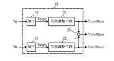
- FIG. 2 is a block diagram showing an example of the three-phase fundamental wave signal generation means 20.
- the three-phase fundamental wave signal generation unit 20 includes a band pass filter 21, a phase adjustment unit 22, and an adder 23.
- the band pass filter 21 is also referred to as a BPF 21.
- the BPF 21 is a filter (fundamental wave component extracting means) that allows only frequency components in a predetermined frequency band to pass among frequency components included in the input signal.
- the frequency band that passes through the BPF 21 is set to the frequency of the system voltage. Accordingly, the BPF 21 receives the U-phase and W-phase voltage signals Vu and Vw of the power system detected by the voltage detector 6 and extracts and outputs the fundamental wave component signals Vubpf and Vvbpf.
- the phase adjusting means 22 receives the signals Vubpf and Vwbpf from the BPF 21, and outputs signals VurefBase and VwrefBase having the same amplitude value as those signals and adjusting a predetermined amount of phase with respect to these signals.
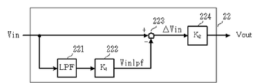
- FIG. 3 is a block diagram showing an example of the phase adjusting means 22.
- the phase adjustment unit 22 includes a low-pass filter 221, multipliers 222 and 224, and an adder 223.
- the low-pass filter 221 is a filter that allows a frequency component in a frequency band lower than the cutoff frequency fc to pass among frequency components included in the input signal.
- the low-pass filter 221 is also referred to as an LPF 221.
- the input signal of the phase adjusting means 22 is Vin
- the output signal is Vout.
- the phase adjusting unit 22 multiplies the signal obtained by inputting the input signal Vin into the LPF 221 by a predetermined coefficient K 1 using the multiplier 222 to generate the signal Vinlpf.
- of the output signal Vout with respect to the input signal Vin of the phase adjusting unit 22 are expressed by the following equations (1) and (2).
- the phase ⁇ of the output signal Vout with respect to the input signal Vin can be adjusted by the coefficient K 1 .
- the phase amount adjusted by the phase adjusting means 22 is the phase generated between the phase of the voltage output from the inverter circuit 10 and the voltage output by the voltage passing through the LC filter composed of the capacitor 8 and the reactor 9. It is a difference.
- may be adjusted by a factor K 2.
- is adjusted so that the ratio of the input signal Vin to the output signal Vout is 1: 1 (gain
- 1).
- the three-phase fundamental wave signal is calculated from the U-phase and W-phase system voltages.
- a wave signal may be calculated.
- each fundamental wave signal may be calculated from the three-phase system voltage.
- the reference signal generator 30 receives the fundamental wave signals Vurefbase, Vvrefbase, and Vwrefbase from the three-phase fundamental wave signal generator 20, and receives a reference cosine wave signal cos ⁇ t (first reference signal) and a reference sine wave signal sin ⁇ t (second second signal). Reference signal).
- FIG. 4 is a block diagram showing an example of the reference signal generating means 30. As shown in FIG.
- the reference signal generation means 30 includes a 120 degree advance signal calculation means 31, a 120 degree delay signal calculation means 32, a reference voltage signal calculation means 33, a reference cosine wave signal calculation means 34, and a reference sine wave signal calculation means 35.
- the 120-degree advance signal calculation means 31 generates a signal whose phase is advanced 120 degrees with respect to the V-phase fundamental wave signal Vvrefbase, that is, a signal in phase with the U-phase fundamental wave signal Vurefbase.
- a signal whose phase is advanced by 120 degrees with respect to the V-phase fundamental wave signal Vvrefbase is, for example, a signal whose phase is advanced by 90 degrees with respect to the fundamental wave signal Vvrefbase from a signal obtained by multiplying the fundamental wave signal Vvrefbase by a coefficient -1/2. It can be calculated by subtracting the signal obtained by multiplying the coefficient ⁇ 3 / 2.
- a signal whose phase is advanced by 90 degrees with respect to the fundamental wave signal Vvrefbase can be obtained, for example, by multiplying a signal obtained by calculating a moving average of the fundamental wave signal Vvrefbase by a coefficient ⁇ / 2.
- the 120-degree delayed signal calculation means 32 generates a signal whose phase is delayed by 120 degrees with respect to the W-phase fundamental wave signal Vwrefbase, that is, a signal in phase with the U-phase fundamental wave signal Vurefbase.
- a signal that is 120 degrees out of phase with respect to the W-phase fundamental wave signal Vwrefbase is, for example, a signal obtained by multiplying the fundamental wave signal Vwrefbase by a coefficient ⁇ 1/2 and a phase that is 90 degrees ahead of the fundamental wave signal Vwrefbase.
- a signal whose phase is advanced by 90 degrees with respect to the fundamental wave signal Vwrefbase can be obtained, for example, by multiplying a signal obtained by calculating a moving average of the fundamental wave signal Vwrefbase by a coefficient ⁇ / 2.
- the reference voltage signal calculation means 33 adds the U-phase fundamental wave signal Vurefbase and the respective signals generated by the 120-degree advance signal calculation means 31 and the 120-degree delay signal calculation means 32, and further adds 1 / 3 is multiplied to generate a reference voltage signal Vref.
- the reference voltage signal Vref generated by the reference voltage signal calculation means 33 is the same in phase as the U-phase fundamental wave signal Vurefbase and the same amplitude value. Become.
- the reference voltage signal Vref generated by the reference voltage signal calculation unit 33 has the same phase as the fundamental wave signal of the phase where the short circuit has not occurred, and the amplitude value is The signal becomes 1/2.
- the reference cosine wave signal calculation means 34 receives the reference voltage signal Vref from the reference voltage signal calculation means 33 and generates a reference cosine wave signal cos ⁇ t.
- the reference cosine wave signal cos ⁇ t is a signal having the same phase as the reference voltage signal Vref and having an amplitude value normalized to 1.
- the reference cosine wave signal cos ⁇ t can be obtained, for example, by dividing the reference voltage signal Vref by its amplitude value.
- the amplitude value of the reference voltage signal Vref can be obtained, for example, by removing the double frequency component of the reference voltage signal Vref from the absolute value signal of the reference voltage signal Vref.
- the double frequency component of the reference voltage signal Vref can be removed by using a moving average calculation, a band elimination filter, a low pass filter, or the like.
- the reference sine wave signal calculation means 35 receives the reference cosine wave signal cos ⁇ t from the reference cosine wave signal calculation means 34 and generates a reference sine wave signal sin ⁇ t whose phase is advanced by 90 degrees from the reference cosine wave signal cos ⁇ t.
- the reference sine wave signal sin ⁇ t can be obtained, for example, by multiplying the moving average value of the reference cosine wave signal cos ⁇ t by a coefficient ⁇ / 2.
- the reference voltage signal calculating means 33 of the reference signal generating means 30 is based on the U-phase fundamental signal Vurefbase, but is based on the V-phase fundamental signal Vvrefbase or the W-phase fundamental signal Vwrefbase. Thus, the reference voltage signal Vref may be calculated.
- the reference signal generation means 30 outputs the calculated reference cosine wave signal cos ⁇ t and reference sine wave signal sin ⁇ t to the coordinate conversion means 14.
- the coordinate conversion means 14 performs coordinate conversion of the active current command Idref and the reactive current command Iqref using the reference cosine wave signal cos ⁇ t and the reference sine wave signal sin ⁇ t, and outputs the U-phase output current command Iuref and the W-phase output current command. Iwref is generated.
- the operation of the output current control means 15 that receives the output current command Iuref and the W-phase output current command Iwref is the same as that of the conventional distributed power supply system described with reference to FIG.
- the reference signal generation means 30 outputs the calculated reference cosine wave signal cos ⁇ t to the third harmonic signal generation means 40.
- the third harmonic signal generation means 40 receives the fundamental wave signals Vurefbase, Vvrefbase, Vwrefbase and the reference cosine wave signal cos ⁇ t as input, and generates a third harmonic signal V3ref.
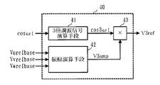
- FIG. 5 is a block diagram showing an example of the third harmonic signal generation means 40.
- the third harmonic signal generation unit 40 includes a third harmonic signal calculation unit 41, an amplitude calculation unit 42, and a multiplier 43.
- the third harmonic signal calculation means 41 calculates a third harmonic signal cos3 ⁇ t with respect to the reference cosine wave signal cos ⁇ t.
- the third harmonic signal cos3 ⁇ t can be calculated with respect to the reference cosine wave signal cos ⁇ t according to the following equation (3).
- the data obtained by multiplying the phase data of the reference cosine wave signal cos ⁇ t by 3 is calculated, and based on this phase data, the value of the cosine wave signal corresponding to the phase data is read out from a pre-stored table to obtain the third harmonic.
- the signal cos3 ⁇ t may be generated.
- the amplitude calculation means 42 calculates the amplitude value V3amp of the third harmonic signal using the fundamental wave signals Vurefbase, Vvrefbase, Vwrefbase. For example, it can be obtained by removing the 6-fold frequency component from the signal obtained by adding the absolute value signals of the fundamental wave signals Vurefbase, Vvrefbase, and Vwrefbase, and further multiplying by a predetermined coefficient.
- the 6-fold frequency component can be removed by using a moving average calculation, a band elimination filter, a low-pass filter, or the like.
- the multiplier 43 multiplies the third harmonic signal cos3 ⁇ t by the amplitude value V3amp of the third harmonic signal to generate a third harmonic signal V3ref.
- the third harmonic signal V3ref is output from the third harmonic signal generator 40 to the three-phase voltage command signal generator 50.
- the three-phase voltage command signal generation means 50 adds the third harmonic signal V3ref to each of the three-phase fundamental wave signals Vurefbase, Vvrefbase, Vwrefbase, and generates voltage command signals Vuref, Vvref, Vwref for each phase.
- the voltage command signals Vuref, Vvref, Vwref of each phase are trapezoidal.
- the voltage command signals Vuref, Vvref, Vwref for each phase are output from the three-phase voltage command signal generation means 50 to the gate signal generation circuit 16.
- the gate signal generation circuit 16 adds the voltage command signals Vuref, Vvref, Vwref of each phase and the correction signals ⁇ Vuref, ⁇ Vvref, ⁇ Vwref corresponding to the voltage commands of each phase for each phase to generate a modulation signal for each phase. To do. Next, the gate signal generation circuit 16 compares the modulation signal of each phase with a predetermined carrier signal, and generates the PWM-modulated control signals G1 to G6. The control signals G1 to G6 are output to the inverter circuit 10.
- the on / off state of the semiconductor switching element of the inverter circuit 10 is controlled based on the control signals G1 to G6 generated by the gate signal generation circuit 16. As a result, a three-phase AC voltage is generated at the output terminal of the inverter circuit 10.
- the three-phase AC voltage output from the inverter circuit 10 can quickly follow the fluctuation of each phase voltage of the power system by the function of the control circuit 101. As a result, even if an instantaneous voltage drop occurs in the power system, the occurrence of overcurrent is prevented.
- the on / off states of the semiconductor switching elements Q1 to Q6 of the inverter circuit 10 are controlled based on the trapezoidally modulated control signals G1 to G6.
- the inverter circuit 10 can effectively use the output voltage of the DC power supply 11. That is, the inverter circuit 10 can output a desired AC voltage even in a region where the generated voltage is lower, such as a solar cell, as compared with the case of performing sine wave modulation.
- the voltage command signals Vuref, Vvref, and Vwref for each phase include a common third harmonic signal V3ref. Therefore, the voltage component caused by the third harmonic signal V3ref is not included in the voltage generated between the AC output terminals of the inverter circuit 10. Therefore, the capacitor 8 and the reactor 9 for removing harmonic components from the output voltage of the inverter circuit 10 do not need to be increased in size.
- the inverter circuit 10 can make the output voltage of the phase not related to the short circuit a trapezoidally modulated voltage. In this case, the inverter circuit 10 does not generate a zero-phase voltage.
- SYMBOLS 1 Three-phase alternating current power supply, 2, 3, 4 ... Switch, 5 ... Load, 6 ... Voltage detector, 7 ... Current detector, 8 ... Capacitor, 9 ... Reactor, 10 ... Inverter circuit, 11 ... DC power supply, 12 ... PLL calculation means, 13, 50 ... Three-phase voltage command signal generation means, 14 ... Coordinate conversion means, 15 ... -Output current control means, 16 ... gate signal generation circuit, 20 ... three-phase fundamental wave signal generation means, 21 ... band pass filter, 22 ... phase adjustment means, 23 ... adder, 30 ... reference signal generation means, 31 ... 120 degree advance signal calculation means, 32 ... 120 degree delay signal calculation means, 33 ...
- reference voltage signal calculation means 34 ... reference cosine wave signal calculation Means 35... Reference sine wave signal calculation means 40... Third harmonic signal Generating means, 41... Triple harmonic signal calculating means, 42... Third harmonic amplitude calculating means, 43... Multiplier, 100, 101. 122 ... dq conversion means, 123 ... proportional integral calculation means, 124 ... VCO means, 125,126 ... adder, 221 ... low-pass filter, 222,224 ... multiplication 223 ... adder.
Landscapes
- Engineering & Computer Science (AREA)
- Power Engineering (AREA)
- Inverter Devices (AREA)
- Supply And Distribution Of Alternating Current (AREA)
Priority Applications (2)
| Application Number | Priority Date | Filing Date | Title |
|---|---|---|---|
| US14/000,720 US9509145B2 (en) | 2011-03-23 | 2012-02-03 | Distributed power supply system |
| CN201280011381.2A CN103430441B (zh) | 2011-03-23 | 2012-02-03 | 分散型电源系统 |
Applications Claiming Priority (2)
| Application Number | Priority Date | Filing Date | Title |
|---|---|---|---|
| JP2011-065002 | 2011-03-23 | ||
| JP2011065002A JP5877648B2 (ja) | 2011-03-23 | 2011-03-23 | 分散型電源システム |
Publications (1)
| Publication Number | Publication Date |
|---|---|
| WO2012127910A1 true WO2012127910A1 (ja) | 2012-09-27 |
Family
ID=46879078
Family Applications (1)
| Application Number | Title | Priority Date | Filing Date |
|---|---|---|---|
| PCT/JP2012/052513 Ceased WO2012127910A1 (ja) | 2011-03-23 | 2012-02-03 | 分散型電源システム |
Country Status (4)
| Country | Link |
|---|---|
| US (1) | US9509145B2 (https=) |
| JP (1) | JP5877648B2 (https=) |
| CN (1) | CN103430441B (https=) |
| WO (1) | WO2012127910A1 (https=) |
Cited By (6)
| Publication number | Priority date | Publication date | Assignee | Title |
|---|---|---|---|---|
| JP2013078180A (ja) * | 2011-09-29 | 2013-04-25 | Daihen Corp | 信号処理装置および信号処理方法 |
| US10110111B2 (en) | 2011-09-29 | 2018-10-23 | Daihen Corporation | Signal processor, filter, control circuit for power converter circuit, interconnection inverter system and PWM converter system |
| CN108964062A (zh) * | 2018-08-17 | 2018-12-07 | 武汉理工大学 | 一种确定分布式潮流控制器3次谐波电流取值范围的方法 |
| US11527948B2 (en) | 2011-09-29 | 2022-12-13 | Daihen Corporation | Signal processor, filter, control circuit for power converter circuit, interconnection inverter system and PWM converter system |
| JP7495654B1 (ja) | 2024-01-26 | 2024-06-05 | 日新電機株式会社 | 電力変換器制御装置、電力変換器の制御方法及び電力変換器の制御プログラム |
| JP7758131B1 (ja) * | 2024-10-24 | 2025-10-22 | 富士電機株式会社 | 電力変換装置および電力変換装置の制御方法 |
Families Citing this family (13)
| Publication number | Priority date | Publication date | Assignee | Title |
|---|---|---|---|---|
| WO2014174667A1 (ja) | 2013-04-26 | 2014-10-30 | 富士電機株式会社 | 共振抑制装置 |
| JP6182032B2 (ja) * | 2013-09-19 | 2017-08-16 | 積水化学工業株式会社 | エネルギマネジメントシステム |
| JP6419977B2 (ja) * | 2015-09-03 | 2018-11-14 | 株式会社東芝 | 電圧変動抑制装置及び方法 |
| KR101755299B1 (ko) | 2015-09-24 | 2017-07-11 | 한국철도기술연구원 | 단상 공진형 무선 전력 전송 시스템의 동기 좌표계 dq 모델링을 이용한 전류 제어 방법 및 이를 이용한 전류 제어 장치 |
| CN105703397B (zh) * | 2016-04-07 | 2018-03-02 | 沈阳农业大学 | 一种考虑农村低压配电网低电压治理的分布式电源优化配置方法 |
| JP7065850B2 (ja) * | 2016-11-30 | 2022-05-12 | コメット アーゲー | 可変電圧発生器回路、システム、及び方法 |
| KR101904101B1 (ko) * | 2016-12-26 | 2018-10-05 | 효성중공업 주식회사 | Mmc 컨버터 출력단 직류성분 제거방법 |
| WO2018211671A1 (ja) * | 2017-05-18 | 2018-11-22 | 東芝三菱電機産業システム株式会社 | 電力変換装置 |
| US10491146B2 (en) * | 2018-03-30 | 2019-11-26 | General Electric Company | System and method for compensating for generator-induced flicker in a wind turbine |
| US11251602B2 (en) * | 2018-07-09 | 2022-02-15 | Schneider Electric Industries Sas | Method for locating an electrical arc fault and electrical installation protection device implementing such a method |
| KR102409013B1 (ko) * | 2018-10-30 | 2022-06-14 | 도시바 미쓰비시덴키 산교시스템 가부시키가이샤 | 전력 변환 장치 |
| CN113196643B (zh) * | 2019-11-26 | 2024-05-10 | 日本精工株式会社 | 马达控制装置、电动致动器产品以及电动助力转向装置 |
| CN119013884A (zh) * | 2022-03-03 | 2024-11-22 | 三菱电机株式会社 | 换流器的控制装置 |
Citations (3)
| Publication number | Priority date | Publication date | Assignee | Title |
|---|---|---|---|---|
| JPH07213069A (ja) * | 1994-01-17 | 1995-08-11 | Fuji Electric Co Ltd | 系統連係インバータの電圧検出回路 |
| JP2003134843A (ja) * | 2001-10-26 | 2003-05-09 | Fuji Electric Co Ltd | Pwm電力変換装置の制御方法 |
| JP2004153957A (ja) * | 2002-10-31 | 2004-05-27 | Hitachi Ltd | 電力変換装置 |
Family Cites Families (7)
| Publication number | Priority date | Publication date | Assignee | Title |
|---|---|---|---|---|
| JP3547355B2 (ja) * | 1999-12-28 | 2004-07-28 | 株式会社日立製作所 | 電力変換システム |
| TWI312218B (en) * | 2005-11-10 | 2009-07-11 | Ablerex Electronics Co Ltd | Islanding detection method for a distributed generation power system |
| JP5364303B2 (ja) * | 2008-06-17 | 2013-12-11 | 山洋電気株式会社 | 電流制御型電力変換器及び電流制御型電力変換器の出力電流波形改善方法 |
| WO2010029808A1 (ja) * | 2008-09-11 | 2010-03-18 | 株式会社ダイヘン | インバータ制御回路、このインバータ制御回路を備えた系統連系インバータシステム |
| JP5226540B2 (ja) * | 2009-01-09 | 2013-07-03 | 株式会社ダイヘン | インバータ制御回路、このインバータ制御回路を備えた系統連系インバータシステム |
| JP5223711B2 (ja) * | 2009-02-10 | 2013-06-26 | 富士電機株式会社 | 無停電電源装置 |
| JP5585371B2 (ja) * | 2010-10-14 | 2014-09-10 | 富士電機株式会社 | 分散型電源システム |
-
2011
- 2011-03-23 JP JP2011065002A patent/JP5877648B2/ja active Active
-
2012
- 2012-02-03 CN CN201280011381.2A patent/CN103430441B/zh not_active Expired - Fee Related
- 2012-02-03 WO PCT/JP2012/052513 patent/WO2012127910A1/ja not_active Ceased
- 2012-02-03 US US14/000,720 patent/US9509145B2/en not_active Expired - Fee Related
Patent Citations (3)
| Publication number | Priority date | Publication date | Assignee | Title |
|---|---|---|---|---|
| JPH07213069A (ja) * | 1994-01-17 | 1995-08-11 | Fuji Electric Co Ltd | 系統連係インバータの電圧検出回路 |
| JP2003134843A (ja) * | 2001-10-26 | 2003-05-09 | Fuji Electric Co Ltd | Pwm電力変換装置の制御方法 |
| JP2004153957A (ja) * | 2002-10-31 | 2004-05-27 | Hitachi Ltd | 電力変換装置 |
Cited By (11)
| Publication number | Priority date | Publication date | Assignee | Title |
|---|---|---|---|---|
| JP2013078180A (ja) * | 2011-09-29 | 2013-04-25 | Daihen Corp | 信号処理装置および信号処理方法 |
| US10110111B2 (en) | 2011-09-29 | 2018-10-23 | Daihen Corporation | Signal processor, filter, control circuit for power converter circuit, interconnection inverter system and PWM converter system |
| US10491101B2 (en) | 2011-09-29 | 2019-11-26 | Daihen Corporation | Signal processor, filter, control circuit for power converter circuit, interconnection inverter system and PWM converter system |
| US10833576B2 (en) | 2011-09-29 | 2020-11-10 | Daihen Corporation | Signal processor, filter, control circuit for power converter circuit, interconnection inverter system and PWM converter system |
| US11381152B2 (en) | 2011-09-29 | 2022-07-05 | Daihen Corporation | Signal processor, filter, control circuit for power converter circuit, interconnection inverter system and PWM converter system |
| US11527948B2 (en) | 2011-09-29 | 2022-12-13 | Daihen Corporation | Signal processor, filter, control circuit for power converter circuit, interconnection inverter system and PWM converter system |
| CN108964062A (zh) * | 2018-08-17 | 2018-12-07 | 武汉理工大学 | 一种确定分布式潮流控制器3次谐波电流取值范围的方法 |
| JP7495654B1 (ja) | 2024-01-26 | 2024-06-05 | 日新電機株式会社 | 電力変換器制御装置、電力変換器の制御方法及び電力変換器の制御プログラム |
| WO2025158685A1 (ja) * | 2024-01-26 | 2025-07-31 | 日新電機株式会社 | 電力変換器制御装置、電力変換器の制御方法及び電力変換器の制御プログラム |
| JP2025115488A (ja) * | 2024-01-26 | 2025-08-07 | 日新電機株式会社 | 電力変換器制御装置、電力変換器の制御方法及び電力変換器の制御プログラム |
| JP7758131B1 (ja) * | 2024-10-24 | 2025-10-22 | 富士電機株式会社 | 電力変換装置および電力変換装置の制御方法 |
Also Published As
| Publication number | Publication date |
|---|---|
| CN103430441B (zh) | 2015-12-23 |
| JP5877648B2 (ja) | 2016-03-08 |
| US9509145B2 (en) | 2016-11-29 |
| CN103430441A (zh) | 2013-12-04 |
| JP2012205325A (ja) | 2012-10-22 |
| US20130328398A1 (en) | 2013-12-12 |
Similar Documents
| Publication | Publication Date | Title |
|---|---|---|
| JP5877648B2 (ja) | 分散型電源システム | |
| JP5585371B2 (ja) | 分散型電源システム | |
| JP2012205325A5 (https=) | ||
| JP5644396B2 (ja) | 電力変換装置の高調波電流抑制装置および高調波電流抑制方法 | |
| JP5542609B2 (ja) | 無効電力補償装置 | |
| EP2621046B1 (en) | System and method for reactive power regulation | |
| JP6159271B2 (ja) | 電力変換装置および電力変換装置の制御方法 | |
| JP5776308B2 (ja) | 系統連系電力変換装置 | |
| JP5580095B2 (ja) | 系統連系インバータ装置 | |
| TWI604697B (zh) | Phase-locked loop method for a utility parallel system | |
| WO2023233454A1 (ja) | 電力変換装置、および制御装置 | |
| JP6583922B2 (ja) | 電力変換装置 | |
| JP6021147B2 (ja) | 風力発電装置 | |
| JP5055184B2 (ja) | 電力変換装置およびその高調波電流抑制方法 | |
| JP2008312372A (ja) | 電力変換装置 | |
| JP6041250B2 (ja) | 系統連系装置 | |
| KR101361574B1 (ko) | 계통연계 전력 공급시스템 및 그 운전 제어방법 | |
| JP6392708B2 (ja) | 自励式電力変換装置 | |
| JP7633865B2 (ja) | インバータの連系方法 | |
| JP2009050091A (ja) | 位相検出装置 | |
| US20140239716A1 (en) | Ac power supply apparatus | |
| JP7322567B2 (ja) | モジュラー・マルチレベル・カスケード変換器 | |
| WO2012176826A1 (ja) | インバータ装置 | |
| JP6327033B2 (ja) | 電力変換装置 | |
| JP2026014458A (ja) | 電力変換装置 |
Legal Events
| Date | Code | Title | Description |
|---|---|---|---|
| 121 | Ep: the epo has been informed by wipo that ep was designated in this application |
Ref document number: 12760041 Country of ref document: EP Kind code of ref document: A1 |
|
| WWE | Wipo information: entry into national phase |
Ref document number: 14000720 Country of ref document: US |
|
| NENP | Non-entry into the national phase |
Ref country code: DE |
|
| 122 | Ep: pct application non-entry in european phase |
Ref document number: 12760041 Country of ref document: EP Kind code of ref document: A1 |