WO2012124106A1 - 差動電流源および差動カレントミラー回路 - Google Patents
差動電流源および差動カレントミラー回路 Download PDFInfo
- Publication number
- WO2012124106A1 WO2012124106A1 PCT/JP2011/056420 JP2011056420W WO2012124106A1 WO 2012124106 A1 WO2012124106 A1 WO 2012124106A1 JP 2011056420 W JP2011056420 W JP 2011056420W WO 2012124106 A1 WO2012124106 A1 WO 2012124106A1
- Authority
- WO
- WIPO (PCT)
- Prior art keywords
- terminal
- transistors
- current source
- differential current
- source
- Prior art date
- Legal status (The legal status is an assumption and is not a legal conclusion. Google has not performed a legal analysis and makes no representation as to the accuracy of the status listed.)
- Ceased
Links
Images






Classifications
-
- G—PHYSICS
- G05—CONTROLLING; REGULATING
- G05F—SYSTEMS FOR REGULATING ELECTRIC OR MAGNETIC VARIABLES
- G05F3/00—Non-retroactive systems for regulating electric variables by using an uncontrolled element, or an uncontrolled combination of elements, such element or such combination having self-regulating properties
- G05F3/02—Regulating voltage or current
-
- H—ELECTRICITY
- H03—ELECTRONIC CIRCUITRY
- H03F—AMPLIFIERS
- H03F1/00—Details of amplifiers with only discharge tubes, only semiconductor devices or only unspecified devices as amplifying elements
- H03F1/26—Modifications of amplifiers to reduce influence of noise generated by amplifying elements
-
- G—PHYSICS
- G05—CONTROLLING; REGULATING
- G05F—SYSTEMS FOR REGULATING ELECTRIC OR MAGNETIC VARIABLES
- G05F3/00—Non-retroactive systems for regulating electric variables by using an uncontrolled element, or an uncontrolled combination of elements, such element or such combination having self-regulating properties
- G05F3/02—Regulating voltage or current
- G05F3/08—Regulating voltage or current wherein the variable is DC
- G05F3/10—Regulating voltage or current wherein the variable is DC using uncontrolled devices with non-linear characteristics
- G05F3/16—Regulating voltage or current wherein the variable is DC using uncontrolled devices with non-linear characteristics being semiconductor devices
- G05F3/20—Regulating voltage or current wherein the variable is DC using uncontrolled devices with non-linear characteristics being semiconductor devices using diode- transistor combinations
- G05F3/26—Current mirrors
- G05F3/262—Current mirrors using field-effect transistors only
-
- H—ELECTRICITY
- H03—ELECTRONIC CIRCUITRY
- H03F—AMPLIFIERS
- H03F3/00—Amplifiers with only discharge tubes or only semiconductor devices as amplifying elements
- H03F3/45—Differential amplifiers
- H03F3/45071—Differential amplifiers with semiconductor devices only
- H03F3/45076—Differential amplifiers with semiconductor devices only characterised by the way of implementation of the active amplifying circuit in the differential amplifier
- H03F3/45179—Differential amplifiers with semiconductor devices only characterised by the way of implementation of the active amplifying circuit in the differential amplifier using MOSFET transistors as the active amplifying circuit
- H03F3/45197—Pl types
-
- H—ELECTRICITY
- H03—ELECTRONIC CIRCUITRY
- H03F—AMPLIFIERS
- H03F2203/00—Indexing scheme relating to amplifiers with only discharge tubes or only semiconductor devices as amplifying elements covered by H03F3/00
- H03F2203/45—Indexing scheme relating to differential amplifiers
- H03F2203/45648—Indexing scheme relating to differential amplifiers the LC comprising two current sources, which are not cascode current sources
Definitions
- the present invention relates to a differential current source and a differential current mirror circuit.
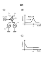
- FIG. 1 is a diagram showing a circuit diagram and noise characteristics of a general current source using an N-channel MOS (Nch) transistor, where (A) shows a circuit diagram and (B) shows noise characteristics.
- Nch N-channel MOS
- the current source includes a transistor Trs and a transistor Trc connected in cascade (series). Trs and Trc are Nch transistors.
- the source of Trs is connected to the power supply (here, ground), and the source of Trc is connected to the drain of Trs.
- a predetermined voltage V1 is applied to the gate of Trs, and a predetermined voltage V2 is applied to the gate of Trc.
- the drain of Trc is the output terminal of the current source.
- Such a current source is widely used as a current source of an analog circuit.
- Nch N channel MOS
- FIG. 1B it is known that 1 / f noise occurs in the output of a current source formed of a MOS transistor.
- the broken line indicates 1 / f noise when the size of the MOS transistor is relatively large, and the solid line indicates 1 / f noise when the size of the MOS transistor is relatively small.
- the 1 / f noise becomes large at a low frequency, so that the SN ratio is deteriorated. Since the 1 / f noise is generally inversely proportional to the 1/2 power of the gate area of the transistor, it is necessary to increase the size of the MOS transistor in order to reduce the 1 / f noise. This increases the chip area and leads to an increase in cost. Therefore, there has been a demand for a current source that reduces 1 / f noise without increasing the size of the MOS transistor.
- differential circuits are mainly used in recent analog circuits.
- a differential OTA Orthogonal Transconductance Amplifier
- a differential current source is used.
- FIG. 2 is a circuit diagram of a general differential current source.
- the differential current source has a first path that outputs a current Ip and a second path that outputs a current Im.
- the first path includes two Nch transistors Tr1 and Tr1c connected in cascade, the source of Tr1 is connected to a power supply (here, ground), and the drain of Tr1c is one output terminal of the differential current source.
- the second path includes two Nch transistors Tr2 and Tr2c connected in cascade, the source of Tr2 is connected to a power supply (here, ground), and the drain of Tr2c is the other output terminal of the differential current source .
- the bias circuit 10 generates a first bias voltage to be applied to the gates of Tr1 and Tr2, and a second bias voltage to be applied to the gates of Tr1c and Tr2c.
- the differential current source of FIG. 2 has a configuration in which two single-phase current sources of FIG. 1 are provided in parallel.
- FIG. 3 is a diagram illustrating an example of use of a differential current source, where (A) is a circuit diagram when in use, (B) is a voltage of input signals Inp and Inm, (C) is an output signal Op and Om current is shown.
- the low-potential side differential current source 100 includes current sources 101 and 102 provided in parallel, and the high-potential side differential current source 200 is provided in parallel.
- Current sources 201 and 202 are included.
- a signal input transistor is connected between the current source 101 and the current source 201, a positive voltage signal Inp of the differential input signal is applied to the gate of the signal input transistor, and a differential is applied from a connection node between the signal input transistor and the current source 201.
- the negative current signal Om of the output signal is obtained.
- a signal input transistor is connected between the current source 102 and the current source 202, the negative voltage signal Inm of the differential input signal is applied to the gate of the signal input transistor, and a differential is applied from the connection node between the signal input transistor and the current source 202.
- a positive current signal Op of the output signal is obtained.
- the differential input signals Inp and Inm are differential voltage signals as shown in FIG.
- the differential output signals Op and Om are differential current signals as shown in FIG.
- the differential current source has the same configuration as the single-phase current source, and 1 / f noise caused by the MOS transistor is generated. Therefore, there has been a demand for a differential current source in which 1 / f noise is reduced without increasing the size of the MOS transistor.
- a differential current source with reduced 1 / f noise is realized by the circuit configuration.
- two source transistors each having a source connected to a power source, a first terminal and a second terminal respectively connected to the drains of the two source transistors, and each being an output terminal
- a mixer circuit having a third terminal and a fourth terminal, wherein the mixer circuit connects the first terminal and the third terminal and connects the second terminal and the fourth terminal in accordance with a local signal.
- a differential current source is provided that changes a connection state between a first connection state and a second connection state in which the first terminal and the fourth terminal are connected and the second terminal and the third terminal are connected.
- two source transistors each having a source connected to a power source, a first terminal and a second terminal respectively connected to the drains of the two source transistors, each being an output terminal
- a mixer circuit having a third terminal and a fourth terminal, wherein the mixer circuit connects the first terminal and the third terminal and connects the second terminal and the fourth terminal according to a local signal.
- a differential current source for changing the connection state between the first connection state and the second connection state in which the first terminal and the fourth terminal are connected and the second terminal and the third terminal are connected, The two terminals are connected to the third terminal and the fourth terminal, respectively, and the other terminal operates as an output terminal of the differential current source, and the gate is shared with the gates of the two cascade transistors.
- two reference transistors one of the two reference transistors is connected between the reference current source and the third terminal, and the other of the two reference transistors is a reference current source.
- a differential current mirror circuit connected between the fourth terminals is provided.
- a differential current source in which 1 / f noise is reduced by a circuit configuration without increasing the size of a MOS transistor is realized.
- FIG. 1A and 1B are a circuit diagram and a noise characteristic of a general current source using an N channel MOS (Nch) transistor.
- FIG. 1A is a circuit diagram and FIG. 1B is a noise characteristic.
- FIG. 2 is a circuit diagram of a general differential current source.
- FIG. 3 is a diagram illustrating an example of use of a differential current source, where (A) is a circuit diagram when in use, (B) is a voltage of a differential input signal, and (C) is a differential output signal. Current is shown.
- FIG. 4 is a circuit diagram of the differential current source according to the first embodiment.
- FIG. 5 is a diagram for explaining the operation of the differential current source according to the first embodiment.
- FIG. 6A and 6B are diagrams for explaining the operating principle of the differential current source according to the first embodiment.
- FIG. 6A is an equivalent circuit
- FIG. 6B is a frequency characteristic after frequency conversion
- FIG. The frequency characteristics of are shown respectively.
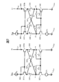
- FIG. 7 is a circuit diagram of a differential current source of a comparative example.
- FIG. 8 is a diagram showing noise simulation results of both circuits when the differential current source of the first embodiment and the circuit of FIG. 7 are configured in the same size.
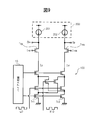
- FIG. 9 is a diagram illustrating a usage example of the differential current source according to the first embodiment.
- FIG. 10 is a circuit diagram of a differential current source according to the second embodiment.
- FIG. 11 is a circuit diagram of a differential current source according to the third embodiment.
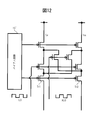
- FIG. 12 is a circuit diagram of the differential current source of the fourth embodiment.
- FIG. 13A is a circuit diagram of a current source for a differential current mirror circuit according to a fifth embodiment
- FIG. 13A is a circuit diagram
- FIG. 13B is a configuration of a general current mirror circuit current source. Indicates.
- FIG. 4 is a circuit diagram of the differential current source according to the first embodiment.
- the differential current source of the first embodiment is a low-potential-side differential current source.
- the differential current source according to the first embodiment includes a first source transistor Tr1, a second source transistor Tr2, a mixer circuit 20, a source that is a mixer (MIXER) circuit 20, a first cascade transistor Tr1c, and a second cascade.
- the transistor Tr2c and the bias circuit 10 are included.
- An example of the bias circuit 10 has the same configuration as the bias circuit shown in FIG.
- the first and second source transistors Tr1 and Tr2 are Nch transistors, and their sources are connected to a low potential power source (ground).
- the mixer circuit 20 includes a first terminal connected to the drain of Tr1, a second terminal connected to the drain of Tr2, a third terminal connected to the source of Tr1c, and a fourth terminal connected to the source of Tr2c. And a terminal.
- the mixer circuit 20 includes a first transistor Tr11 connected between the first terminal and the third terminal, a second transistor Tr12 connected between the second terminal and the fourth terminal, and a first terminal and a fourth terminal. And a fourth transistor Tr14 connected between the second terminal and the third terminal. Tr11 to Tr14 are Nch transistors.
- Tr11 and Tr12 operate in the opposite phase to Tr13 and Tr14. In other words, when Tr11 and Tr12 are in the on (conducting) state, Tr13 and Tr14 are in the off (shut-off) state, and when Tr11 and Tr12 are in the off state, Tr13 and Tr14 are in the on state.
- the differential local signal has a higher frequency than the frequency range targeted by the circuit using the differential current source of the first embodiment.
- the first cascade transistor Tr1c is an Nch transistor, the source is connected to the third terminal of the mixer circuit 20, and the drain operates as the output terminal of the differential current source.
- the second cascade transistor Tr2c is an Nch transistor, the source is connected to the fourth terminal of the mixer circuit 20, and the drain operates as the output terminal of the differential current source.
- the differential current source according to the first embodiment has a configuration in which a normal cascade-connected current source is provided in parallel and the mixer circuit 20 is inserted between two source transistors and two cascade transistors.
- Have The mixer circuit 20 is driven with a local signal LO / XLO that is higher than the required signal band.
- FIG. 5 is a diagram for explaining the operation of the differential current source according to the first embodiment.
- Tr11 and Tr12 are turned on, and Tr13 and Tr14 are turned off. Become. Thereby, a path passing through Tr1, Tr11, and Tr1c is formed, and the current of Tr1 is output as the output current Ip. At the same time, a path passing through Tr2, Tr12, and Tr2c is formed, and the current of Tr2 is output as the output current Im.
- Tr11 and Tr12 are turned off and Tr13 and Tr14 are turned on. Thereby, a path passing through Tr1, Tr13, and Tr2c is formed, and the current of Tr1 is output as the output current Im. At the same time, a path passing through Tr2, Tr14 and Tr1c is formed, and the current of Tr2 is output as the output current Ip.
- Tr1 and Tr2 are switched and output according to the polarity of the local signal.
- This can be represented by an equivalent circuit as shown in FIG.
- Noise generated from Tr1 and Tr2 is output as Ip and Im through the mixer circuit 20. Therefore, the 1 / f noise in the low frequency region shown in FIG. 6C generated from Tr1 and Tr2 is converted into the frequency of the local signal LO / XLO as shown in FIG. Shifted to the side.
- the 1 / f noise is reduced in the low frequency region, the SN ratio of the low frequency signal is improved. Since noise is converted into a high frequency outside the signal band, the SN ratio does not deteriorate.
- Patent Document 1 describes a current mirror circuit in which the influence of a difference in threshold voltage of transistors is reduced by switching the path connection at a predetermined frequency in the reference path and the operation path of the current mirror circuit. Yes.
- FIG. 7 is a diagram showing a circuit configuration conceivable when the configuration described in Patent Document 1 is applied to a differential current source. Since the two paths of the differential current source are operation paths, it is conceivable to switch the connection using the two paths as double paths. For this reason, the number of elements increases.
- the differential current source according to the first embodiment focuses on the fact that the two paths are operation paths, but the connection between them can be switched. Switching is realized with a small number of elements.
- the switch of the mixer circuit -Six transistors are required. That is, six transistors are required for one of the differential current sources.
- the mixer circuit of the differential current source is composed of four transistors, and one of the differential current sources can be composed of two transistors.
- the circuit shown in FIG. 7 has a problem that noise generated from the cascade transistor 330 is added to the output current and noise is increased. This is for the following operation.
- a potential difference related to noise generated in the Tr 330b also occurs between b and d.
- I_noise_a and I_noise_b are current values of different current paths, differential noise currents resulting from Tr 330a and Tr 330b are output to Ip and Im. In other words, when the two paths of the differential current source are respectively double paths, the noise frequency conversion by switching the connection is performed by the independent double paths.
- Tr2c a potential due to the noise of Tr2c is generated at the connection node between Tr1, Tr11, and Tr13, and the connection between Tr2, Tr12, and Tr14 is generated.
- a potential due to the noise of Tr1c is generated at the node.
- the same amount of noise current caused by the potential difference between the two nodes is output to both Ip and Im, a low-frequency differential current caused by the noise of Tr1c and Tr2c is not generated.
- FIG. 8 is a diagram showing noise simulation results of both circuits when the differential current source of the first embodiment and the circuit of FIG. 7 are configured in the same size, and P is the differential current of the first embodiment.
- the source case is shown when Q is the circuit of FIG.
- R indicates the noise subjected to frequency conversion that appears in the switching frequency in the differential current source according to the first embodiment.
- FIG. 8 shows that 1 / f noise is reduced in the low frequency region.
- FIG. 9 is a diagram illustrating a usage example of the differential current source according to the first embodiment.
- the portion denoted by reference numeral 100 is the differential current source of the first embodiment that functions as a low-potential side differential current source, and 200 is the high-potential side differential current source.
- the signal input transistors Trip and Trim Is connected.
- One Inp of the differential input signal is applied to the gate of Trip, and the other Inm of the differential input signal is applied to the gate of Trim.
- the output Om is output from a connection node between one current source 201 of the high potential side differential current source and Trip, and the output Op is output from a connection node between the other current source 202 of the high potential side differential current source and Trim. Is done.
- FIG. 10 is a circuit diagram of the differential current source of the second embodiment.
- the transistors of the mixer circuit 20 of the first embodiment are Pch transistors Tr21-Tr24, and the differential local signals LO and XLO are applied to the Tr21-Tr24 via the high-pass filter 30.
- the high-pass filter 30 is connected to two resistors connected between the gates of Tr21 and Tr22 and the ground and between the gates of Tr23 and Tr24 and the ground, and to a connection node between the gate and the resistor of Tr21-Tr24, respectively. Two capacities.
- the differential local signals LO and XLO are supplied through two capacitors, respectively.
- 1 / f noise is mainly generated in Tr1 and Tr2, but is also generated to some extent in the four Nch transistors Tr11-Tr14 of the mixer circuit 20 and increases noise.
- 1 / f noise generated in an Nch transistor is larger than 1 / f noise generated in a Pch transistor. Therefore, in the second embodiment, the generation of noise is suppressed by using the transistors of the mixer circuit 20 as Pch transistors Tr21 to Tr24.
- the noise of the differential current source of the second embodiment is further reduced compared to the differential current source of the first embodiment.
- FIG. 11 is a circuit diagram of the differential current source of the third embodiment.
- the configuration in which the capacitor C of the third embodiment is provided is also effective in the first embodiment.
- differential current source of the first to third embodiments is a low-potential side differential current source
- the configuration can be similarly applied to a high-potential side differential current source.
- FIG. 12 is a circuit diagram of the differential current source of the fourth embodiment.
- the differential current source of the fourth embodiment is a high potential side differential current source.
- the differential current source of the fourth embodiment is different from the differential current source of the first embodiment of FIG. 4 in that the transistors Tr1, Tr2, Tr11-Tr14, Tr1c, and Tr2c are changed from Nch transistors to Pch transistors. .
- the bias circuit 10 'generates a voltage suitable for the Pch transistor.
- FIG. 13A is a circuit diagram of the differential current mirror circuit of the fifth embodiment
- FIG. 13B is a diagram showing a configuration of a general folded cascade type current mirror circuit.
- the current mirror circuit on the low potential side includes a common transistor Trx, a reference pass transistor Trr, and an operation pass transistor Trc.
- the common transistor Trx is an Nch transistor, and its source is connected to the ground.
- the reference pass transistor Trr is an Nch transistor, the source is connected to the drain of the Trx, and the drain is connected to the reference current path.
- the reference current path is connected to a reference current source.
- the operation pass transistor Trc is an Nch transistor, the source is connected to the drain of the Trx, the drain is connected to the operation path, and a current is output.
- the differential current mirror circuit of the fifth embodiment is different from the second embodiment in that reference pass transistors Tr1r and Tr2r are provided in parallel with the cathode transistors Tr1c and Tr2c in the differential current source of the second embodiment.
- a voltage applied to the gates of the cathode transistors Tr1c and Tr2c generated in the bias circuit 10 is commonly applied to the gates of the reference pass transistors Tr1r and Tr2r.
- the reference pass transistor Tr1r is connected between the first reference path and a connection node between Tr1c and the third terminals (Tr21 and Tr24).
- the reference path transistor Tr2r is connected between the second reference path and a connection node between Tr2c and the fourth terminal (Tr22 and Tr23).
- the first reference current Iref_p flows through the first reference path
- the second reference current Iref_m flows through the second reference path.
- the first reference path to which Tr1r is connected and the path to which the drain of Tr1c is connected form a current mirror circuit
- Iref_p and Ip have a relationship of current mirror signals.
- the second reference path to which Tr2r is connected and the path to which the drain of Tr2c is connected form a current mirror circuit
- Iref_m and Im have a relationship between current mirror signals.
- a current mirror circuit with low 1 / f noise can be configured.
Landscapes
- Engineering & Computer Science (AREA)
- Physics & Mathematics (AREA)
- Power Engineering (AREA)
- Microelectronics & Electronic Packaging (AREA)
- Electromagnetism (AREA)
- General Physics & Mathematics (AREA)
- Radar, Positioning & Navigation (AREA)
- Automation & Control Theory (AREA)
- Nonlinear Science (AREA)
- Amplifiers (AREA)
- Control Of Electrical Variables (AREA)
Abstract
差動電流源は、ソースがそれぞれ電源に接続された2個のソーストランジスタと、2個のソーストランジスタのドレインにそれぞれ接続された第1端子および第2端子と、それぞれが出力端子である第3端子および第4端子と、を有するミキサ回路と、を備え、ミキサ回路は、ローカル信号に応じて、第1端子と第3端子を接続すると共に第2端子と第4端子を接続した第1接続状態と、第1端子と第4端子を接続すると共に第2端子と第3端子を接続した第2接続状態と、の間で接続状態を変化させ、1/fノイズを低減する。
Description
本発明は、差動電流源および差動カレントミラー回路に関する。
アナログ回路では、電流源が広く使用される。
図1は、NチャネルMOS(Nch)トランジスタを使用した一般的な電流源の回路図およびノイズ特性を示す図であり、(A)が回路図を、(B)がノイズ特性を示す。
図1の(A)に電流源の一例を示す。電流源は、カスケード(直列)接続されたトランジスタTrsおよびトランジスタTrcを有する。TrsおよびTrcは、Nchトランジスタである。Trsは、ソースが電源(ここではグランド)に接続され、Trcは、ソースがTrsのドレインに接続される。Trsのゲートには所定の電圧V1が印加され、Trcのゲートには所定の電圧V2が印加される。Trcのドレインが電流源の出力端子である。このような電流源は、アナログ回路の電流源として広く使用されている。
なお、Nchトランジスタの代わりに、Pchトランジスタが使用された電流源もある。以下、NチャネルMOS(Nch)を使用した電流源を例として説明を行う。
図1の(B)に示すように、MOSトランジスタで形成される電流源は、出力に1/fノイズが発生することが知られている。図1の(B)において、破線はMOSトランジスタのサイズが相対的に大きな場合の1/fノイズを、実線はMOSトランジスタのサイズが相対的に小さな場合の1/fノイズを、それぞれ示す。
このような電流源を使用する回路で必要な信号が低周波成分の場合、この1/fノイズは低周波で大きくなるため、SN比を劣化させる。1/fノイズは、一般的にトランジスタのゲート面積の1/2乗に反比例するため、1/fノイズを小さくするためには、MOSトランジスタのサイズを大きくする必要があった。これは、チップ面積を増大させ、コストアップにつながる。そのため、MOSトランジスタのサイズを大きくせずに1/fノイズを低減した電流源が要望されていた。
一方、近年のアナログ回路では差動回路が主流であり、例えば差動型のOTA(Operational Transconductance Amplifier)を使用した回路では、差動電流源が使用される。
図2は、一般的な差動電流源の回路図である。この差動電流源は、図2に示すように、電流Ipを出力する第1のパスと、電流Imを出力する第2のパスと、を有する。第1のパスは、カスケード接続した2個のNchトランジスタTr1およびTr1cを有し、Tr1のソースが電源(ここではグランド)に接続され、Tr1cのドレインが差動電流源の一方の出力端子である。第2のパスは、カスケード接続した2個のNchトランジスタTr2およびTr2cを有し、Tr2のソースが電源(ここではグランド)に接続され、Tr2cのドレインが差動電流源の他方の出力端子である。バイアス回路10は、Tr1およびTr2のゲートに印加する第1バイアス電圧と、Tr1cおよびTr2cのゲートに印加する第2バイアス電圧と、を発生する。言い換えれば、図2の差動電流源は、図1の単相の電流源を2つ並列に設けた構成を有する。
図3は、差動電流源の使用例を示す図であり、(A)が使用時の回路図であり、(B)が入力信号InpおよびInmの電圧を、(C)が出力信号OpおよびOmの電流を、示す。図3の(A)に示すように、低電位側差動電流源100は、並列に設けられた電流源101および102を有し、高電位側差動電流源200は、並列に設けられた電流源201および202を有する。電流源101と電流源201の間に信号入力トランジスタが接続され、信号入力トランジスタのゲートに差動入力信号の正側電圧信号Inpが印加され、信号入力トランジスタと電流源201の接続ノードから差動出力信号の負側電流信号Omが得られる。電流源102と電流源202の間に信号入力トランジスタが接続され、信号入力トランジスタのゲートに差動入力信号の負側電圧信号Inmが印加され、信号入力トランジスタと電流源202の接続ノードから差動出力信号の正側電流信号Opが得られる。
差動入力信号InpおよびInmは、図3の(B)に示すように、差動電圧信号である。差動出力信号OpおよびOmは、図3の(C)に示すように、差動電流信号である。
図2に示すように、差動電流源は、単相電流源と同様の構成を有しており、MOSトランジスタに起因する1/fノイズが発生する。そのため、MOSトランジスタのサイズを大きくせずに1/fノイズを低減した差動電流源が要望されていた。
実施形態によれば、回路構成により1/fノイズを低減した差動電流源が実現される。
発明の一観点によれば、ソースがそれぞれ電源に接続された2個のソーストランジスタと、2個のソーストランジスタのドレインにそれぞれ接続された第1端子および第2端子と、それぞれが出力端子である第3端子および第4端子と、を有するミキサ回路と、を有し、ミキサ回路は、ローカル信号に応じて、第1端子と第3端子を接続すると共に第2端子と第4端子を接続した第1接続状態と、第1端子と第4端子を接続すると共に第2端子と第3端子を接続した第2接続状態と、の間で接続状態を変化させる差動電流源が提供される。
発明の別の観点によれば、ソースがそれぞれ電源に接続された2個のソーストランジスタと、2個のソーストランジスタのドレインにそれぞれ接続された第1端子および第2端子と、それぞれが出力端子である第3端子および第4端子と、を有するミキサ回路と、を有し、ミキサ回路は、ローカル信号に応じて、第1端子と第3端子を接続すると共に第2端子と第4端子を接続した第1接続状態と、第1端子と第4端子を接続すると共に第2端子と第3端子を接続した第2接続状態と、の間で接続状態を変化させる差動電流源と、一方の端子が第3端子および第4端子にそれぞれ接続され、他方の端子がそれぞれ差動電流源の出力端子として動作する2個のカスケードトランジスタと、ゲートが2個のカスケードトランジスタのゲートと共通に接続された2個の参照トランジスタと、を有し、2個の参照トランジスタの一方は、参照電流源と第3端子の間に接続され、2個の参照トランジスタの他方は、参照電流源と第4端子の間に接続された差動カレントミラー回路が提供される。
発明の観点によれば、MOSトランジスタのサイズを大きくせずに、回路構成により1/fノイズを低減した差動電流源が実現される。
図4は、第1実施形態の差動電流源の回路図である。第1実施形態の差動電流源は、低電位側の差動電流源である。
第1実施形態の差動電流源は、第1ソーストランジスタTr1と、第2ソーストランジスタTr2と、ミキサ回路20と、ソースがミキサ(MIXER)回路20と、第1カスケードトランジスタTr1cと、第2カスケードトランジスタTr2cと、バイアス回路10と、を有する。バイアス回路10の一例は、図2に示したバイアス回路と同じ構成を有する。
第1および第2ソーストランジスタTr1、Tr2は、Nchトランジスタで、ソースが低電位側電源(グランド)に接続されている。
ミキサ回路20は、Tr1のドレインに接続される第1端子と、Tr2のドレインに接続される第2端子と、Tr1cのソースに接続される第3端子と、Tr2cのソースに接続される第4端子と、を有する。ミキサ回路20は、第1端子と第3端子の間に接続された第1トランジスタTr11と、第2端子と第4端子の間に接続された第2トランジスタTr12と、第1端子と第4端子の間に接続された第3トランジスタTr13と、第2端子と第3端子の間に接続された第4トランジスタTr14と、を有する。Tr11からTr14は、Nchトランジスタである。
第1トランジスタTr11および第2トランジスタTr12のゲートには、差動ローカル信号の一方の信号LOが印加される。第3トランジスタTr13および第4トランジスタTr14のゲートには、差動ローカル信号の他方の信号XLOが印加される。これにより、Tr11およびTr12は、Tr13およびTr14と逆相で動作する。言い換えれば、Tr11およびTr12がオン(導通)状態の時には、Tr13およびTr14はオフ(遮断)状態であり、Tr11およびTr12がオフ状態の時には、Tr13およびTr14はオン状態である。
差動ローカル信号は、第1実施形態の差動電流源を使用する回路が対象とする周波数範囲より、高い周波数であることが望ましい。
第1カスケードトランジスタTr1cは、Nchトランジスタであり、ソースがミキサ回路20の第3端子に接続され、ドレインが差動電流源の出力端子として動作する。第2カスケードトランジスタTr2cは、Nchトランジスタであり、ソースがミキサ回路20の第4端子に接続され、ドレインが差動電流源の出力端子として動作する。
このように、第1実施形態の差動電流源は、通常のカスケード接続された電流源を並列に設け、2個のソーストランジスタと2個のカスケードトランジスタの間に、ミキサ回路20を挿入した構成を有する。ミキサ回路20は、必要な信号帯域より高いローカル信号LO/XLOで駆動される。
図5は、第1実施形態の差動電流源の動作を説明する図である。
ローカル信号の一方の信号LOが“H”で、他方の信号XLOが“L”の場合、図5の(A)に示すように、Tr11およびTr12がオン状態に、Tr13およびTr14がオフ状態になる。これにより、Tr1、Tr11およびTr1cを通るパスが形成され、Tr1の電流は出力電流Ipとして出力される。同時に、Tr2、Tr12およびTr2cを通るパスが形成され、Tr2の電流は出力電流Imとして出力される。
次に、LOが“L”で、他方の信号XLOが“H”の場合、図5の(B)に示すように、Tr11およびTr12がオフ状態に、Tr13およびTr14がオン状態になる。これにより、Tr1、Tr13およびTr2cを通るパスが形成され、Tr1の電流は出力電流Imとして出力される。同時に、Tr2、Tr14およびTr1cを通るパスが形成され、Tr2の電流は出力電流Ipとして出力される。
このように、ローカル信号の極性によって、Tr1とTr2の電流が入れ替わって出力される。これを等価回路で表わすと図6の(A)に示すようになる。Tr1およびTr2から発生するノイズは、ミキサ回路20を通してIp、Imとして出力されることになる。したがって、Tr1およびTr2から発生した図6の(C)に示した低周波領域の1/fノイズは、図6の(B)に示すように、ローカル信号LO/XLOの周波数に変換され、高周波側にシフトされる。これにより、低周波領域では1/fノイズが削減されるため低周波信号のSN比が向上する。ノイズは信号帯域外の高周波に変換されるためSN比の劣化を引き起こさない。
特許文献1は、カレントミラー回路の参照パスと動作パスの2つのパスにおいて、パスの接続を所定の周波数で切り換えることにより、トランジスタの閾値電圧の差による影響を低減したカレントミラー回路を記載している。
図7は、特許文献1に記載された構成を差動電流源に適用した場合に考えられる回路構成を示す図である。差動電流源の2つのパスは動作パスであるため、2つのパスをそれぞれ2重パスとして、接続を切り換えることが考えられる。そのため、素子数の増加を招くことになる。
これに対して、第1実施形態の差動電流源は、2つのパスは動作パスであるが、その接続を切り換えることが可能であることに着目したものであり、差動電流源における接続の切り換えを、少ない素子数で実現するものである。
例えば、図7に示すように、特許文献1に記載された構成を適用して、差動電流源の2つのパスをそれぞれ2重パスとして、接続を切り換えるミキサ回路を設ける場合、ミキサ回路のスイッチ・トランジスタは6個必要である。すなわち、差動電流源の一方について6個のトランジスタが必要になる。これに対して、第1実施形態では、差動電流源のミキサ回路は4個のトランジスタで構成され、差動電流源の一方については2個のトランジスタで構成できる。
また、図7に示す回路では、カスケードトランジスタ330から発生するノイズが出力電流に加算されてノイズが増加するという問題がある。これは、次のような動作のためである。
・Tr330aに発生するノイズにより、aとcの電位がずれる。
・この電位差に起因する電流I_noise_aが、スイッチング周期ごとに発生する。
・bとdの間にも、Tr330bに発生するノイズに関係した電位差が発生する。
・この電位差に起因する電流I_noise_bが、スイッチング周期ごとに発生する。
・I_noise_aとI_noise_bは、異なった電流パスの電流値であるため、IpとImにはTr330aおよびTr330bに起因した差動ノイズ電流が出力される。言い換えれば、差動電流源の2つのパスをそれぞれ2重パスとした場合、接続の切り換えによるノイズの周波数変換は、それぞれの独立した2重パスで行うためである。
これに対して、第1実施形態の差動電流源では、Tr1と、Tr11およびTr13と、の接続ノードにはTr2cのノイズに起因する電位が発生し、Tr2と、Tr12およびTr14と、の接続ノードにはTr1cのノイズに起因する電位が発生する。しかし、IpおよびImには両方とも、上記の2つのノードの電位差に起因する同量のノイズ電流が出力されるため、Tr1cおよびTr2cのノイズに起因した低周波の差動電流は発生しない。
図8は、第1実施形態の差動電流源と図7の回路を同サイズで構成した場合の、両回路のノイズ・シミュレーション結果を示す図であり、Pが第1実施形態の差動電流源の場合を、Qが図7の回路の場合を示す。図8で、Rは、第1実施形態の差動電流源でスイッチング周波数に現れる周波数変換されたノイズを示す。図8から、低周波数領域において、1/fノイズが低減されることが分かる。
図9は、第1実施形態の差動電流源の使用例を示す図である。参照番号100で示す部分が、低電位側差動電流源として働く第1実施形態の差動電流源であり、200が高電位側差動電流源であり、その間に、信号入力トランジスタTripおよびTrimが接続される。Tripのゲートには差動入力信号の一方Inpが印加され、Trimのゲートには差動入力信号の他方Inmが印加される。出力Omは、高電位側差動電流源の一方の電流源201とTripの接続ノードから出力され、出力Opは、高電位側差動電流源の他方の電流源202とTrimの接続ノードから出力される。
図10は、第2実施形態の差動電流源の回路図である。
第2実施形態の差動電流源では、第1実施形態のミキサ回路20のトランジスタを、PchトランジスタTr21-Tr24とし、差動ローカル信号LOおよびXLOを、ハイパスフィルタ30を介してTr21-Tr24に印加することが、第1実施形態と異なる。ハイパスフィルタ30は、Tr21およびTr22のゲートとグランドの間およびTr23およびTr24のゲートとグランドの間にそれぞれ接続された2個の抵抗と、Tr21-Tr24のゲートと抵抗の接続ノードにそれぞれ接続された2個の容量と、を有する。差動ローカル信号LOおよびXLOは、2個の容量の容量を介してそれぞれ供給される。
第1実施形態の差動電流源において、1/fノイズは、Tr1およびTr2で主として発生するが、ミキサ回路20の4個のNchトランジスタTr11-Tr14でもある程度発生し、ノイズを増加させる。一般に、Nchトランジスタで発生する1/fノイズの方が、Pchトランジスタで発生する1/fノイズより大きいことが知られている。そこで、第2実施形態では、ミキサ回路20のトランジスタを、PchトランジスタTr21-Tr24として、ノイズの発生を抑制している。
そのため、第2実施形態の差動電流源は、第1実施形態の差動電流源に比べて、ノイズが一層低減される。
図11は、第3実施形態の差動電流源の回路図である。
第3実施形態の差動電流源では、第2実施形態において、ミキサ回路20の第3端子と第4端子間、すなわち、Tr21およびTr24とTr1cの接続ノードと、Tr22およびTr23とTr2cの接続ノードと、の間に、容量Cを接続することが異なる。容量Cを設けることにより、ミキサ回路からのスイッチングノイズ(ローカルリーク)を削減することができる。
なお、第3実施形態の容量Cを設ける構成は、第1実施形態でも同様に有効である。
第1から第3実施形態の差動電流源は、低電位側差動電流源であったが、その構成は、高電位側差動電流源にも同様に適用可能である。
図12は、第4実施形態の差動電流源の回路図である。第4実施形態の差動電流源は、高電位側差動電流源である。第4実施形態の差動電流源は、図4の第1実施形態の差動電流源において、トランジスタTr1、Tr2、Tr11-Tr14、Tr1cおよびTr2cを、NchトランジスタからPchトランジスタに変更したことが異なる。バイアス回路10’は、Pchトランジスタに適合した電圧を発生する。
図13の(A)は、第5実施形態の差動カレントミラー回路の回路図であり、図13の(B)は、一般的な折り返しカスケード型カレントミラー回路の構成を示す図である。
図13の(B)に示すように、低電位側のカレントミラー回路は、共通トランジスタTrxと、参照パストランジスタTrrと、動作パストランジスタTrcと、を有する。共通トランジスタTrxは、Nchトランジスタで、ソースがグランドに接続される。参照パストランジスタTrrは、Nchトランジスタで、ソースがTrxのドレインに接続され、ドレインが参照電流パスに接続される。参照電流パスは、参照電流源に接続される。動作パストランジスタTrcは、Nchトランジスタで、ソースがTrxのドレインに接続され、ドレインが動作パスに接続され、電流が出力される。
第5実施形態の差動カレントミラー回路は、第2実施形態の差動電流源において、カソードトランジスタTr1cおよびTr2cと並列に参照パストランジスタTr1rおよびTr2rを設けたことが第2実施形態と異なる。参照パストランジスタTr1rおよびTr2rのゲートには、バイアス回路10で発生されたカソードトランジスタTr1cおよびTr2cのゲートに印加される電圧が共通に印加される。参照パストランジスタTr1rは、第1の参照パスと、Tr1cと第3端子(Tr21およびTr24)の接続ノードと、の間に接続される。参照パストランジスタTr2rは、第2の参照パスと、Tr2cと第4端子(Tr22およびTr23)の接続ノードと、の間に接続される。第1の参照パスには、第1の参照電流Iref_pが流れ、第2の参照パスには、第2の参照電流Iref_mが流れる。Tr1rが接続される第1の参照パスとTr1cのドレインが接続されるパスがカレントミラー回路を形成し、Iref_pとIpがカレントミラー信号の関係になる。Tr2rが接続される第2の参照パスとTr2cのドレインが接続されるパスがカレントミラー回路を形成し、Iref_mとImがカレントミラー信号の関係になる。
図13の(A)の第5実施形態の差動カレントミラー回路を使用することにより、1/fノイズが小さいカレントミラー回路を構成できる。
以上、実施形態を説明したが、ここに記載したすべての例や条件は、発明および技術に適用する発明の概念の理解を助ける目的で記載されたものであり、特に記載された例や条件は発明の範囲を制限することを意図するものではなく、明細書のそのような例の構成は発明の利点および欠点を示すものではない。発明の実施形態を詳細に記載したが、各種の変更、置き換え、変形が発明の精神および範囲を逸脱することなく行えることが理解されるべきである。
10 バイアス回路
20 ミキサ回路
Tr1,Tr2 ソーストランジスタ
Tr1c,Tr2c カソードトランジスタ
Tr11-Tr14 ミキサ回路トランジスタ
20 ミキサ回路
Tr1,Tr2 ソーストランジスタ
Tr1c,Tr2c カソードトランジスタ
Tr11-Tr14 ミキサ回路トランジスタ
Claims (10)
- ソースがそれぞれ電源に接続された2個のソーストランジスタと、
前記2個のソーストランジスタのドレインにそれぞれ接続された第1端子および第2端子と、それぞれが出力端子である第3端子および第4端子と、を有するミキサ回路と、を備え、
前記ミキサ回路は、ローカル信号に応じて、前記第1端子と前記第3端子を接続すると共に前記第2端子と前記第4端子を接続した第1接続状態と、前記第1端子と前記第4端子を接続すると共に前記第2端子と前記第3端子を接続した第2接続状態と、の間で接続状態を変化させることを特徴とする差動電流源。 - 一方の端子が前記第3端子および前記第4端子にそれぞれ接続され、他方の端子がそれぞれ当該差動電流源の出力端子として動作する2個のカスケードトランジスタを備える請求項1記載の差動電流源。
- 前記ミキサ回路は、
前記第1端子と前記第3端子の間に接続された第1トランジスタと、
前記第2端子と前記第4端子の間に接続された第2トランジスタと、
前記第1端子と前記第4端子の間に接続された第3トランジスタと、
前記第2端子と前記第3端子の間に接続された第4トランジスタと、を備え、
前記ローカル信号は、差動ローカル信号であり、
前記差動ローカル信号の一方が、前記第1トランジスタおよび前記第2トランジスタのゲートに印加され、
前記差動ローカル信号の他方が、前記第3トランジスタおよび前記第4トランジスタのゲートに印加される請求項1または2記載の差動電流源。 - 前記差動ローカル信号は、抵抗と容量を含むハイパスフィルタを介して、前記第1から第4トランジスタのゲートに印加される請求項3記載の差動電流源。
- 前記ミキサ回路の前記第1から第4トランジスタは、前記2個のソーストランジスタと同じ極性のトランジスタである請求項1から4のいずれか1項記載の差動電流源。
- 前記ミキサ回路の前記第1から第4トランジスタは、前記2個のソーストランジスタと異なる極性のトランジスタである請求項1から4のいずれか1項記載の差動電流源。
- 前記第3端子と前記第4端子の間に接続された容量を備える請求項1から6のいずれか1項記載の差動電流源。
- 前記2個のソーストランジスタおよび前記ミキサ回路の前記第1から第4トランジスタは、Nチャネルトランジスタである請求項5記載の差動電流源。
- 前記2個のソーストランジスタは、Nチャネルトランジスタであり、前記ミキサ回路の前記第1から第4トランジスタはPチャネルトランジスタである請求項6記載の差動電流源。
- ソースがそれぞれ電源に接続された2個のソーストランジスタと、前記2個のソーストランジスタのドレインにそれぞれ接続された第1端子および第2端子と、それぞれが出力端子である第3端子および第4端子と、を有するミキサ回路と、を備え、前記ミキサ回路は、ローカル信号に応じて、前記第1端子と前記第3端子を接続すると共に前記第2端子と前記第4端子を接続した第1接続状態と、前記第1端子と前記第4端子を接続すると共に前記第2端子と前記第3端子を接続した第2接続状態と、の間で接続状態を変化させる差動電流源と、
一方の端子が前記第3端子および前記第4端子にそれぞれ接続され、他方の端子がそれぞれ前記差動電流源の出力端子として動作する2個のカスケードトランジスタと、
ゲートが前記2個のカスケードトランジスタのゲートと共通に接続された2個の参照トランジスタと、を備え、
前記2個の参照トランジスタの一方は、参照電源と前記第3端子の間に接続され、
前記2個の参照トランジスタの他方は、前記参照電源と前記第4端子の間に接続された差動カレントミラー回路。
Priority Applications (3)
| Application Number | Priority Date | Filing Date | Title |
|---|---|---|---|
| PCT/JP2011/056420 WO2012124106A1 (ja) | 2011-03-17 | 2011-03-17 | 差動電流源および差動カレントミラー回路 |
| JP2013504483A JPWO2012124106A1 (ja) | 2011-03-17 | 2011-03-17 | 差動電流源および差動カレントミラー回路 |
| US14/026,938 US20140009139A1 (en) | 2011-03-17 | 2013-09-13 | Differential current source and differential current mirror circuit |
Applications Claiming Priority (1)
| Application Number | Priority Date | Filing Date | Title |
|---|---|---|---|
| PCT/JP2011/056420 WO2012124106A1 (ja) | 2011-03-17 | 2011-03-17 | 差動電流源および差動カレントミラー回路 |
Related Child Applications (1)
| Application Number | Title | Priority Date | Filing Date |
|---|---|---|---|
| US14/026,938 Continuation US20140009139A1 (en) | 2011-03-17 | 2013-09-13 | Differential current source and differential current mirror circuit |
Publications (1)
| Publication Number | Publication Date |
|---|---|
| WO2012124106A1 true WO2012124106A1 (ja) | 2012-09-20 |
Family
ID=46830234
Family Applications (1)
| Application Number | Title | Priority Date | Filing Date |
|---|---|---|---|
| PCT/JP2011/056420 Ceased WO2012124106A1 (ja) | 2011-03-17 | 2011-03-17 | 差動電流源および差動カレントミラー回路 |
Country Status (3)
| Country | Link |
|---|---|
| US (1) | US20140009139A1 (ja) |
| JP (1) | JPWO2012124106A1 (ja) |
| WO (1) | WO2012124106A1 (ja) |
Families Citing this family (2)
| Publication number | Priority date | Publication date | Assignee | Title |
|---|---|---|---|---|
| DE102018204782A1 (de) * | 2018-03-28 | 2019-10-02 | Robert Bosch Gmbh | Detektorschaltung und System zur galvanisch-getrennten Übertragung digitaler Signale |
| US10636709B2 (en) * | 2018-04-10 | 2020-04-28 | International Business Machines Corporation | Semiconductor fins with dielectric isolation at fin bottom |
Citations (2)
| Publication number | Priority date | Publication date | Assignee | Title |
|---|---|---|---|---|
| JP2006129416A (ja) * | 2004-09-28 | 2006-05-18 | Sharp Corp | 電圧−電流変換回路、それを用いた増幅器、ミキサ回路および携帯機器 |
| US20070013438A1 (en) * | 2005-07-13 | 2007-01-18 | Texas Instruments Incorporated | Chopper-stabilized operational amplifier and method |
Family Cites Families (3)
| Publication number | Priority date | Publication date | Assignee | Title |
|---|---|---|---|---|
| US7000A (en) * | 1850-01-08 | Smut-machine | ||
| US5444363A (en) * | 1993-12-16 | 1995-08-22 | Advanced Micro Devices Inc. | Low noise apparatus for receiving an input current and producing an output current which mirrors the input current |
| JP5088235B2 (ja) * | 2008-05-26 | 2012-12-05 | 富士通株式会社 | ノイズキャンセル回路及びノイズキャンセル回路付き増幅器 |
-
2011
- 2011-03-17 JP JP2013504483A patent/JPWO2012124106A1/ja active Pending
- 2011-03-17 WO PCT/JP2011/056420 patent/WO2012124106A1/ja not_active Ceased
-
2013
- 2013-09-13 US US14/026,938 patent/US20140009139A1/en not_active Abandoned
Patent Citations (2)
| Publication number | Priority date | Publication date | Assignee | Title |
|---|---|---|---|---|
| JP2006129416A (ja) * | 2004-09-28 | 2006-05-18 | Sharp Corp | 電圧−電流変換回路、それを用いた増幅器、ミキサ回路および携帯機器 |
| US20070013438A1 (en) * | 2005-07-13 | 2007-01-18 | Texas Instruments Incorporated | Chopper-stabilized operational amplifier and method |
Also Published As
| Publication number | Publication date |
|---|---|
| US20140009139A1 (en) | 2014-01-09 |
| JPWO2012124106A1 (ja) | 2014-07-17 |
Similar Documents
| Publication | Publication Date | Title |
|---|---|---|
| JP5431992B2 (ja) | トランスミッションゲート及び半導体装置 | |
| CN115225067B (zh) | 基于运放的迟滞比较器和芯片 | |
| WO2016051473A1 (ja) | 演算増幅回路 | |
| KR20120095246A (ko) | 레벨 쉬프터 | |
| US7795975B2 (en) | Class AB amplifier | |
| US8217721B1 (en) | Slew rate enhancing circuit | |
| JP4928290B2 (ja) | 差動信号比較器 | |
| JP5566211B2 (ja) | スイッチドキャパシタ型d/aコンバータ | |
| TWI504139B (zh) | 運算放大器電路 | |
| TW201838327A (zh) | 跨導放大器 | |
| WO2012124106A1 (ja) | 差動電流源および差動カレントミラー回路 | |
| JP2015141462A (ja) | 基準電圧回路 | |
| US7538585B2 (en) | Transconductor | |
| US8604878B2 (en) | Folded cascode amplifier with an enhanced slew rate | |
| Baxevanakis et al. | Rail-to-rail operational amplifier with stabilized frequency response and constant-gm input stage | |
| JP2014007471A (ja) | ヒステリシスコンパレータ回路及びヒステリシスコンパレータ回路の制御方法 | |
| US9191006B1 (en) | Current-limited level shift circuit | |
| JP7479753B2 (ja) | 差動増幅器 | |
| US7157946B2 (en) | Chopper comparator circuit | |
| JP2012156826A (ja) | コンパレータ | |
| CN103825567A (zh) | 运算放大器电路 | |
| JP2012114610A (ja) | 電子回路 | |
| JP5203809B2 (ja) | 電流ミラー回路 | |
| JP6845680B2 (ja) | アナログスイッチ回路 | |
| TWI835651B (zh) | 放大器電路 |
Legal Events
| Date | Code | Title | Description |
|---|---|---|---|
| 121 | Ep: the epo has been informed by wipo that ep was designated in this application |
Ref document number: 11860839 Country of ref document: EP Kind code of ref document: A1 |
|
| ENP | Entry into the national phase |
Ref document number: 2013504483 Country of ref document: JP Kind code of ref document: A |
|
| NENP | Non-entry into the national phase |
Ref country code: DE |
|
| 122 | Ep: pct application non-entry in european phase |
Ref document number: 11860839 Country of ref document: EP Kind code of ref document: A1 |