WO2012121255A1 - 半導体装置 - Google Patents
半導体装置 Download PDFInfo
- Publication number
- WO2012121255A1 WO2012121255A1 PCT/JP2012/055707 JP2012055707W WO2012121255A1 WO 2012121255 A1 WO2012121255 A1 WO 2012121255A1 JP 2012055707 W JP2012055707 W JP 2012055707W WO 2012121255 A1 WO2012121255 A1 WO 2012121255A1
- Authority
- WO
- WIPO (PCT)
- Prior art keywords
- semiconductor
- esd protection
- protection element
- semiconductor device
- insulating film
- Prior art date
- Legal status (The legal status is an assumption and is not a legal conclusion. Google has not performed a legal analysis and makes no representation as to the accuracy of the status listed.)
- Ceased
Links
Images








Classifications
-
- H—ELECTRICITY
- H10—SEMICONDUCTOR DEVICES; ELECTRIC SOLID-STATE DEVICES NOT OTHERWISE PROVIDED FOR
- H10D—INORGANIC ELECTRIC SEMICONDUCTOR DEVICES
- H10D89/00—Aspects of integrated devices not covered by groups H10D84/00 - H10D88/00
- H10D89/60—Integrated devices comprising arrangements for electrical or thermal protection, e.g. protection circuits against electrostatic discharge [ESD]
- H10D89/601—Integrated devices comprising arrangements for electrical or thermal protection, e.g. protection circuits against electrostatic discharge [ESD] for devices having insulated gate electrodes, e.g. for IGFETs or IGBTs
- H10D89/811—Integrated devices comprising arrangements for electrical or thermal protection, e.g. protection circuits against electrostatic discharge [ESD] for devices having insulated gate electrodes, e.g. for IGFETs or IGBTs using FETs as protective elements
- H10D89/819—Bias arrangements for gate electrodes of FETs, e.g. RC networks or voltage partitioning circuits
-
- H—ELECTRICITY
- H10—SEMICONDUCTOR DEVICES; ELECTRIC SOLID-STATE DEVICES NOT OTHERWISE PROVIDED FOR
- H10D—INORGANIC ELECTRIC SEMICONDUCTOR DEVICES
- H10D84/00—Integrated devices formed in or on semiconductor substrates that comprise only semiconducting layers, e.g. on Si wafers or on GaAs-on-Si wafers
- H10D84/01—Manufacture or treatment
- H10D84/02—Manufacture or treatment characterised by using material-based technologies
- H10D84/03—Manufacture or treatment characterised by using material-based technologies using Group IV technology, e.g. silicon technology or silicon-carbide [SiC] technology
- H10D84/038—Manufacture or treatment characterised by using material-based technologies using Group IV technology, e.g. silicon technology or silicon-carbide [SiC] technology using silicon technology, e.g. SiGe
-
- H—ELECTRICITY
- H10—SEMICONDUCTOR DEVICES; ELECTRIC SOLID-STATE DEVICES NOT OTHERWISE PROVIDED FOR
- H10D—INORGANIC ELECTRIC SEMICONDUCTOR DEVICES
- H10D30/00—Field-effect transistors [FET]
- H10D30/60—Insulated-gate field-effect transistors [IGFET]
- H10D30/67—Thin-film transistors [TFT]
- H10D30/674—Thin-film transistors [TFT] characterised by the active materials
- H10D30/6755—Oxide semiconductors, e.g. zinc oxide, copper aluminium oxide or cadmium stannate
-
- H—ELECTRICITY
- H10—SEMICONDUCTOR DEVICES; ELECTRIC SOLID-STATE DEVICES NOT OTHERWISE PROVIDED FOR
- H10D—INORGANIC ELECTRIC SEMICONDUCTOR DEVICES
- H10D62/00—Semiconductor bodies, or regions thereof, of devices having potential barriers
- H10D62/80—Semiconductor bodies, or regions thereof, of devices having potential barriers characterised by the materials
-
- H—ELECTRICITY
- H10—SEMICONDUCTOR DEVICES; ELECTRIC SOLID-STATE DEVICES NOT OTHERWISE PROVIDED FOR
- H10D—INORGANIC ELECTRIC SEMICONDUCTOR DEVICES
- H10D62/00—Semiconductor bodies, or regions thereof, of devices having potential barriers
- H10D62/80—Semiconductor bodies, or regions thereof, of devices having potential barriers characterised by the materials
- H10D62/875—Semiconductor bodies, or regions thereof, of devices having potential barriers characterised by the materials being semiconductor metal oxide, e.g. InGaZnO
-
- H—ELECTRICITY
- H10—SEMICONDUCTOR DEVICES; ELECTRIC SOLID-STATE DEVICES NOT OTHERWISE PROVIDED FOR
- H10D—INORGANIC ELECTRIC SEMICONDUCTOR DEVICES
- H10D84/00—Integrated devices formed in or on semiconductor substrates that comprise only semiconducting layers, e.g. on Si wafers or on GaAs-on-Si wafers
-
- H—ELECTRICITY
- H10—SEMICONDUCTOR DEVICES; ELECTRIC SOLID-STATE DEVICES NOT OTHERWISE PROVIDED FOR
- H10D—INORGANIC ELECTRIC SEMICONDUCTOR DEVICES
- H10D86/00—Integrated devices formed in or on insulating or conducting substrates, e.g. formed in silicon-on-insulator [SOI] substrates or on stainless steel or glass substrates
- H10D86/40—Integrated devices formed in or on insulating or conducting substrates, e.g. formed in silicon-on-insulator [SOI] substrates or on stainless steel or glass substrates characterised by multiple TFTs
- H10D86/411—Integrated devices formed in or on insulating or conducting substrates, e.g. formed in silicon-on-insulator [SOI] substrates or on stainless steel or glass substrates characterised by multiple TFTs characterised by materials, geometry or structure of the substrates
-
- H—ELECTRICITY
- H10—SEMICONDUCTOR DEVICES; ELECTRIC SOLID-STATE DEVICES NOT OTHERWISE PROVIDED FOR
- H10D—INORGANIC ELECTRIC SEMICONDUCTOR DEVICES
- H10D86/00—Integrated devices formed in or on insulating or conducting substrates, e.g. formed in silicon-on-insulator [SOI] substrates or on stainless steel or glass substrates
- H10D86/40—Integrated devices formed in or on insulating or conducting substrates, e.g. formed in silicon-on-insulator [SOI] substrates or on stainless steel or glass substrates characterised by multiple TFTs
- H10D86/421—Integrated devices formed in or on insulating or conducting substrates, e.g. formed in silicon-on-insulator [SOI] substrates or on stainless steel or glass substrates characterised by multiple TFTs having a particular composition, shape or crystalline structure of the active layer
- H10D86/423—Integrated devices formed in or on insulating or conducting substrates, e.g. formed in silicon-on-insulator [SOI] substrates or on stainless steel or glass substrates characterised by multiple TFTs having a particular composition, shape or crystalline structure of the active layer comprising semiconductor materials not belonging to the Group IV, e.g. InGaZnO
-
- H—ELECTRICITY
- H10—SEMICONDUCTOR DEVICES; ELECTRIC SOLID-STATE DEVICES NOT OTHERWISE PROVIDED FOR
- H10D—INORGANIC ELECTRIC SEMICONDUCTOR DEVICES
- H10D86/00—Integrated devices formed in or on insulating or conducting substrates, e.g. formed in silicon-on-insulator [SOI] substrates or on stainless steel or glass substrates
- H10D86/40—Integrated devices formed in or on insulating or conducting substrates, e.g. formed in silicon-on-insulator [SOI] substrates or on stainless steel or glass substrates characterised by multiple TFTs
- H10D86/441—Interconnections, e.g. scanning lines
-
- H—ELECTRICITY
- H10—SEMICONDUCTOR DEVICES; ELECTRIC SOLID-STATE DEVICES NOT OTHERWISE PROVIDED FOR
- H10D—INORGANIC ELECTRIC SEMICONDUCTOR DEVICES
- H10D86/00—Integrated devices formed in or on insulating or conducting substrates, e.g. formed in silicon-on-insulator [SOI] substrates or on stainless steel or glass substrates
- H10D86/40—Integrated devices formed in or on insulating or conducting substrates, e.g. formed in silicon-on-insulator [SOI] substrates or on stainless steel or glass substrates characterised by multiple TFTs
- H10D86/60—Integrated devices formed in or on insulating or conducting substrates, e.g. formed in silicon-on-insulator [SOI] substrates or on stainless steel or glass substrates characterised by multiple TFTs wherein the TFTs are in active matrices
-
- H—ELECTRICITY
- H10—SEMICONDUCTOR DEVICES; ELECTRIC SOLID-STATE DEVICES NOT OTHERWISE PROVIDED FOR
- H10D—INORGANIC ELECTRIC SEMICONDUCTOR DEVICES
- H10D88/00—Three-dimensional [3D] integrated devices
-
- H—ELECTRICITY
- H10—SEMICONDUCTOR DEVICES; ELECTRIC SOLID-STATE DEVICES NOT OTHERWISE PROVIDED FOR
- H10D—INORGANIC ELECTRIC SEMICONDUCTOR DEVICES
- H10D89/00—Aspects of integrated devices not covered by groups H10D84/00 - H10D88/00
- H10D89/60—Integrated devices comprising arrangements for electrical or thermal protection, e.g. protection circuits against electrostatic discharge [ESD]
- H10D89/601—Integrated devices comprising arrangements for electrical or thermal protection, e.g. protection circuits against electrostatic discharge [ESD] for devices having insulated gate electrodes, e.g. for IGFETs or IGBTs
- H10D89/611—Integrated devices comprising arrangements for electrical or thermal protection, e.g. protection circuits against electrostatic discharge [ESD] for devices having insulated gate electrodes, e.g. for IGFETs or IGBTs using diodes as protective elements
-
- H—ELECTRICITY
- H10—SEMICONDUCTOR DEVICES; ELECTRIC SOLID-STATE DEVICES NOT OTHERWISE PROVIDED FOR
- H10D—INORGANIC ELECTRIC SEMICONDUCTOR DEVICES
- H10D89/00—Aspects of integrated devices not covered by groups H10D84/00 - H10D88/00
- H10D89/60—Integrated devices comprising arrangements for electrical or thermal protection, e.g. protection circuits against electrostatic discharge [ESD]
- H10D89/601—Integrated devices comprising arrangements for electrical or thermal protection, e.g. protection circuits against electrostatic discharge [ESD] for devices having insulated gate electrodes, e.g. for IGFETs or IGBTs
- H10D89/931—Integrated devices comprising arrangements for electrical or thermal protection, e.g. protection circuits against electrostatic discharge [ESD] for devices having insulated gate electrodes, e.g. for IGFETs or IGBTs characterised by the dispositions of the protective arrangements
-
- H—ELECTRICITY
- H10—SEMICONDUCTOR DEVICES; ELECTRIC SOLID-STATE DEVICES NOT OTHERWISE PROVIDED FOR
- H10P—GENERIC PROCESSES OR APPARATUS FOR THE MANUFACTURE OR TREATMENT OF DEVICES COVERED BY CLASS H10
- H10P14/00—Formation of materials, e.g. in the shape of layers or pillars
- H10P14/40—Formation of materials, e.g. in the shape of layers or pillars of conductive or resistive materials
-
- H—ELECTRICITY
- H10—SEMICONDUCTOR DEVICES; ELECTRIC SOLID-STATE DEVICES NOT OTHERWISE PROVIDED FOR
- H10W—GENERIC PACKAGES, INTERCONNECTIONS, CONNECTORS OR OTHER CONSTRUCTIONAL DETAILS OF DEVICES COVERED BY CLASS H10
- H10W42/00—Arrangements for protection of devices
- H10W42/20—Arrangements for protection of devices protecting against electromagnetic or particle radiation, e.g. light, X-rays, gamma-rays or electrons
-
- H—ELECTRICITY
- H10—SEMICONDUCTOR DEVICES; ELECTRIC SOLID-STATE DEVICES NOT OTHERWISE PROVIDED FOR
- H10W—GENERIC PACKAGES, INTERCONNECTIONS, CONNECTORS OR OTHER CONSTRUCTIONAL DETAILS OF DEVICES COVERED BY CLASS H10
- H10W42/00—Arrangements for protection of devices
- H10W42/60—Arrangements for protection of devices protecting against electrostatic charges or discharges, e.g. Faraday shields
-
- H—ELECTRICITY
- H10—SEMICONDUCTOR DEVICES; ELECTRIC SOLID-STATE DEVICES NOT OTHERWISE PROVIDED FOR
- H10W—GENERIC PACKAGES, INTERCONNECTIONS, CONNECTORS OR OTHER CONSTRUCTIONAL DETAILS OF DEVICES COVERED BY CLASS H10
- H10W20/00—Interconnections in chips, wafers or substrates
- H10W20/40—Interconnections external to wafers or substrates, e.g. back-end-of-line [BEOL] metallisations or vias connecting to gate electrodes
-
- H—ELECTRICITY
- H10—SEMICONDUCTOR DEVICES; ELECTRIC SOLID-STATE DEVICES NOT OTHERWISE PROVIDED FOR
- H10W—GENERIC PACKAGES, INTERCONNECTIONS, CONNECTORS OR OTHER CONSTRUCTIONAL DETAILS OF DEVICES COVERED BY CLASS H10
- H10W20/00—Interconnections in chips, wafers or substrates
- H10W20/40—Interconnections external to wafers or substrates, e.g. back-end-of-line [BEOL] metallisations or vias connecting to gate electrodes
- H10W20/41—Interconnections external to wafers or substrates, e.g. back-end-of-line [BEOL] metallisations or vias connecting to gate electrodes characterised by their conductive parts
- H10W20/435—Cross-sectional shapes or dispositions of interconnections
-
- H—ELECTRICITY
- H10—SEMICONDUCTOR DEVICES; ELECTRIC SOLID-STATE DEVICES NOT OTHERWISE PROVIDED FOR
- H10W—GENERIC PACKAGES, INTERCONNECTIONS, CONNECTORS OR OTHER CONSTRUCTIONAL DETAILS OF DEVICES COVERED BY CLASS H10
- H10W20/00—Interconnections in chips, wafers or substrates
- H10W20/40—Interconnections external to wafers or substrates, e.g. back-end-of-line [BEOL] metallisations or vias connecting to gate electrodes
- H10W20/45—Interconnections external to wafers or substrates, e.g. back-end-of-line [BEOL] metallisations or vias connecting to gate electrodes characterised by their insulating parts
- H10W20/47—Interconnections external to wafers or substrates, e.g. back-end-of-line [BEOL] metallisations or vias connecting to gate electrodes characterised by their insulating parts comprising two or more dielectric layers having different properties, e.g. different dielectric constants
Definitions
- the present invention relates to a semiconductor device, and in particular, ESD (electro-static).
- ESD electro-static
- the present invention relates to a semiconductor device including a discharge protection element.
- an ESD protection element is integrated in a semiconductor device including an integrated circuit in order to protect the integrated circuit from ESD.
- an active element such as a transistor or a diode in order to obtain an active action such as a variable resistor.
- FIG. 1 is a cross-sectional view showing an example of the configuration of such a semiconductor device.
- the semiconductor device 100 in FIG. 1 includes a logic region 100A and an ESD protection element region 100B.
- the logic area 100A is an area where a logic circuit and other integrated circuits are formed.
- a semiconductor element 102 such as a MOS transistor is formed in the logic region 100A of the semiconductor substrate 101, and a plurality of (six layers in FIG. 1) wiring layers 103 are provided above the semiconductor element 102.
- Each wiring layer 103 is formed with a wiring 104 and an interlayer insulating film 105 that electrically isolates the wiring 104 of the adjacent wiring layer 103.
- the wiring 104 of the wiring layer 103 located on the lowermost side with the semiconductor element 102 and the wirings 104 of the two adjacent wiring layers 103 are electrically connected by a via 106 provided through the interlayer insulating film 105.
- An integrated circuit is formed by the semiconductor element 102, the wiring 104 and the via 106.
- the ESD protection element region 100B is a region where the ESD protection element 107 is formed.
- An ESD protection element 107 is formed in the ESD protection element region 100B of the semiconductor substrate 101.
- An active element is used as the ESD protection element 107.
- a thyristor having a PNPN structure is formed as the ESD protection element 107.
- the ESD protection element 107 is connected to an I / O pad and a ground pad provided in the uppermost wiring layer 103 via a wiring 104 and a via 106 provided in each wiring layer 103.
- the wiring connected to the I / O pad is denoted by reference numeral 108
- the wiring connected to the ground pad is denoted by reference numeral 109.
- One problem of a semiconductor device using a transistor or a diode formed on a semiconductor substrate as an ESD protection element as shown in FIG. 1 is that the chip area is increased due to the formation of the ESD protection element. Since the ESD protection element is formed on the semiconductor substrate, it is necessary to provide a region for forming the ESD protection element separately from a region for forming the integrated circuit. This leads to an increase in chip area. Moreover, since a large current can flow through the ESD protection element when an ESD surge is applied, it is necessary to form a transistor or a diode having a large area as the ESD protection element. This makes the problem of increasing chip area increasingly serious.
- Japanese Patent Application Laid-Open No. 2010-141230 discloses a technique in which a semiconductor layer is provided in a wiring layer and a semiconductor element is formed using the semiconductor layer.
- the material of the semiconductor layer include oxide semiconductors such as InGaZnO (IGZO) and ZnO, polysilicon, and amorphous silicon.
- IGZO InGaZnO
- ZnO zinc-oxide
- polysilicon silicon
- amorphous silicon silicon
- a transistor which is a switching element is cited.
- a technique in which a trap film and a back gate electrode are provided on the semiconductor element, and the semiconductor element is used as a memory element.
- Japanese Unexamined Patent Application Publication No. 2010-141230 does not mention any ESD protection.
- Japanese Patent Application Laid-Open Nos. 2010-41058, 2010-98280, and 2010-135762 disclose thin film transistors including an oxide semiconductor film.
- a thin film transistor including an oxide semiconductor film is used in a liquid crystal display device or other active matrix display devices.
- an object of the present invention is to reduce the chip size of a semiconductor device provided with an ESD protection element.
- a semiconductor device is provided on a semiconductor substrate on which a semiconductor element is formed, first and second pads, a first insulating film formed above the semiconductor substrate, and a first insulating film.
- a plurality of wirings embedded in the trench, a second insulating film provided so as to cover the first insulating film and the plurality of wirings, a semiconductor layer formed on the second insulating film, and a semiconductor A source electrode connected to the layer; and a drain electrode connected to the semiconductor layer.
- the plurality of wirings include a gate electrode provided at a position facing the semiconductor layer.
- the semiconductor layer, the source electrode, the drain electrode, and the gate electrode constitute an ESD protection element that discharges current due to an ESD surge from the first pad to the second pad.
- the chip size of a semiconductor device provided with an ESD protection element can be reduced.
- FIG. 3 is a cross-sectional view showing a structure in the vicinity of an ESD protection element of the semiconductor device of FIG. 2.
- FIG. 3 is a layout diagram illustrating a planar layout of an ESD protection element in the semiconductor device of FIG. 2.
- FIG. 4B is a layout diagram illustrating a planar layout of an ESD protection element in the semiconductor device of FIG. 4B.
- FIG. 5 is a graph showing the relationship between the thickness of a SiN film used as a gate insulating film and the gate-drain breakdown voltage. It is sectional drawing which shows the structure of the ESD protection element in which the drain electrode overlaps with the gate electrode among the measured ESD protection elements. It is sectional drawing which shows the structure of the ESD protection element from which the position of the edge of a drain electrode corresponds with the position of the edge of a gate electrode in planar structure among the measured ESD protection elements. It is sectional drawing which shows the structure of the ESD protection element from which the drain electrode does not overlap with the gate electrode among the measured ESD protection elements.
- FIG. 6 is a graph showing drain current characteristics of an ESD protection element including a 20 nm SiN film as a gate insulating film and having overlap lengths of 0.16 ⁇ m, 0.0 ⁇ m, and ⁇ 0.16 ⁇ m.
- 4 is a graph showing drain current characteristics of an ESD protection element including a 30 nm SiN film as a gate insulating film and having an overlap length of 0.16 ⁇ m, 0.0 ⁇ m, and ⁇ 0.16 ⁇ m.
- 5 is a graph showing drain current characteristics of an ESD protection element including a 50 nm SiN film as a gate insulating film and having overlap lengths of 0.16 ⁇ m, 0.0 ⁇ m, and ⁇ 0.16 ⁇ m.
- FIG. 10 is a graph showing the relationship between the overlap length of the ESD protection element of FIGS. 9A to 9C and the gate-drain breakdown voltage. It is a circuit diagram which shows an example of the circuit structure which uses an ESD protection element for protection of an internal circuit. It is sectional drawing which shows the example of the structure of the semiconductor device of the circuit structure of FIG. It is a circuit diagram which shows the other example of the circuit structure which uses an ESD protection element for protection of an internal circuit. It is sectional drawing which shows the example of the structure of the semiconductor device of the circuit structure of FIG.
- FIG. 2 is a cross-sectional view showing the configuration of the semiconductor device 10 according to an embodiment of the present invention.
- a semiconductor element 2 such as a MOS transistor is formed on the surface portion of the semiconductor substrate 1, and a plurality of wiring layers 3 are formed thereabove.
- a silicon substrate is used as the semiconductor substrate 1.
- Each wiring layer 3 includes an interlayer insulating film 4 and wiring 5 embedded in a wiring groove provided on the surface thereof.
- the wiring 5 in the uppermost wiring layer 3 is an aluminum wiring, and the wirings 5 in other wiring layers 3 are copper wirings.
- the number of wiring layers 3 is eight.
- a low dielectric constant insulating layer having a dielectric constant lower than that of silicon oxide is used as the interlayer insulating film 4.
- Examples of the low dielectric constant insulating layer include an SiOC film, an SiLK film (SiLK is a registered trademark), an HSQ (hydrogensilsesquioxane) film, an MHSQ (methylated hydrogensilsesquioxane) film, and an MSQ (methyl).
- SiLK SiLK is a registered trademark
- HSQ hydrogensilsesquioxane
- MHSQ methylated hydrogensilsesquioxane
- MSQ methyl
- the uppermost wiring layer 3 may be referred to as a wiring layer 3-1
- the second wiring layer 3 from the top may be referred to as a wiring layer 3-3
- the uppermost interlayer insulating film 4 may be referred to as an interlayer insulating film 4-1
- the second interlayer insulating film 4 from the top may be referred to as an interlayer insulating film 4-2.
- the diffusion prevention layer 7 is an insulating film for preventing diffusion of the material of the wiring 5 (particularly, copper constituting the copper wiring).
- the diffusion preventing layer 7 for example, a SiN film, a SiO 2 film, and a SiCN film can be used.
- the thickness of the diffusion preventing layer 7 is, for example, 10 to 50 nm.
- the uppermost diffusion prevention layer 7 may be referred to as a diffusion prevention layer 7-1.
- FIG. 3 is a cross-sectional view showing the structure of the semiconductor device 10 around the ESD protection element 11 and its periphery.
- the wirings 5-1 and 5-2 are both copper wirings, and are formed using the damascene method in the same wiring forming process.
- the wiring 5-2 is used as a gate electrode of a thin film transistor used as the ESD protection element 11. Therefore, hereinafter, the wiring 5-2 may be referred to as the gate electrode 13.
- the semiconductor layer 12 is formed on the upper surface of the diffusion preventing layer 7-1 so as to face the gate electrode 13.
- the semiconductor layer 12 is formed of an oxide semiconductor such as InGaZnO (IGZO), InZnO (IZO), ZnO, ZnAlO, or ZnCuO.
- IGZO InGaZnO
- IZO InZnO
- ZnO ZnAlO
- ZnCuO ZnCuO.
- These oxide semiconductors can be formed at a relatively low temperature (for example, at a temperature of 400 ° C. or lower).
- a wiring located below the semiconductor layer 12 is used.
- the semiconductor layer 12 can be formed at a temperature suitable for a wiring process generally used for forming the layer 3.
- a hard mask layer 14 is formed on the semiconductor layer 12.
- the hard mask layer 14 is an insulating film used as a mask in the process of patterning the semiconductor layer 12.
- a SiO 2 film or a SiN film is used as the hard mask layer 14.
- the hard mask layer 14 also serves to suppress the reduction of the semiconductor layer 12 in the manufacturing process of the semiconductor device 10.
- the uppermost interlayer insulating film 4-1 is formed so as to cover the semiconductor layer 12 and the hard mask layer 14.
- barrier metal layers 8-3 to 8-5 are formed in contact with the wiring 5-1 belonging to the wiring layer 3-2, and the barrier metal layers 8-4 and 8-5 are in contact with the semiconductor layer 12. Formed.
- the material of the barrier metal layers 8-3 to 8-5 include Ti, Ta, Ru, W, nitrides or oxides thereof.
- the barrier metal layers 8-3 to 8-5 may be a single-layer film made of these materials, or may be a laminate of two or more layers.
- Examples of the laminated barrier metal layers 8-3 to 8-5 include, for example, a laminate of TiN (upper layer) / Ti (lower layer) or TaN (upper layer) / Ta (lower layer).
- the barrier metal layers 8-3 to 8-5 are collectively formed in the same formation process.
- the barrier metal layers 8-4 to 8-5 are formed so that an ohmic contact is formed at a contact portion with the semiconductor layer 12.
- Wirings 5-3 to 5-5 and vias 6-3 to 6-5 are formed in the wiring grooves and via holes covered with the barrier metal layers 8-3 to 8-5, respectively.
- the wirings 5-3 to 5-5 are all wirings belonging to the wiring layer 3-1.
- the wirings 5-3 to 5-5 and the vias 6-3 to 6-5 are collectively formed in the same formation process.
- the wiring 5-3 is connected to the wiring 5-1 of the wiring layer 3-2 through the via 6-3.
- the wirings 5-4 and 5-5 are connected to the semiconductor layer 12 through vias 6-4 and 6-5, respectively.
- the wiring 5-4, the via 6-4, and the barrier metal layer 8-4 are used as a source electrode of a thin film transistor used as the ESD protection element 11.
- these may be collectively referred to as the source electrode 15.
- the wiring 5-5, the via 6-5, and the barrier metal layer 8-5 are used as the drain electrode of the thin film transistor.
- these may be collectively referred to as the drain electrode 16.
- the wiring 5-1, 5-3 and the via 6-3 are components of an integrated circuit integrated in the semiconductor device 10.
- the semiconductor layer 12, the gate electrode 13, the source electrode 15, the drain electrode 16, and the diffusion prevention layer 7-1 constitute a thin film transistor.
- a portion of the diffusion prevention layer 7-1 located between the semiconductor layer 12 and the gate electrode 13 functions as a gate insulating film.
- the thin film transistor having such a configuration is used as the ESD protection element 11.
- the semiconductor layer 12 is formed of an oxide semiconductor such as InGaZnO (IGZO), InZnO (IZO), ZnO, ZnAlO, or ZnCuO
- the semiconductor layer 12 is an n-type semiconductor
- the ESD protection element 11 has electrons as carriers. Operates as a thin film transistor.
- FIG. 4A is a plan view showing an example of a planar layout of the semiconductor layer 12, the gate electrode 13, the source electrode 15, and the drain electrode 16.
- the x-axis is defined in the direction from the source electrode 15 to the drain electrode 16, and the y-axis is defined perpendicular to the x-axis.
- a portion of the semiconductor layer 12 between the source electrode 15 and the drain electrode 16 faces the gate electrode 13, and this portion is used as a channel region.
- the contact surfaces of the source electrode 15, the drain electrode 16, and the semiconductor layer 12 have the same rectangular shape, and the distance between the source electrode 15 and the drain electrode 16 along the semiconductor layer 12 is the same as that of the thin film transistor.
- the gate width W is the gate length L, and the width in the y-axis direction of the contact surface of the source electrode 15, the drain electrode 16, and the semiconductor layer 12.
- FIG. 4A shows a planar layout in which a part of the source electrode 15 and the drain electrode 16 overlaps the gate electrode 13.
- the overlap length of the source electrode 15 with respect to the gate electrode 13 is indicated by a symbol d OL1
- the overlap length of the drain electrode 16 with respect to the gate electrode 13 is indicated by a symbol d OL2 .
- the overlap length is a distance in the in-plane direction from the end of the source electrode 15 or the drain electrode 16 to the end of the gate electrode 13.
- a planar layout in which the source electrode 15 and the drain electrode 16 do not overlap with the gate electrode 13 may be used.
- the drain electrode 16 does not overlap the gate electrode 13 (that is, the contact surface between the drain electrode 16 and the semiconductor layer 12 is the gate electrode in the vertical direction of the semiconductor substrate 1).
- Adopting a structure that does not overlap 13) is effective for increasing the breakdown voltage between the drain electrode 16 and the gate electrode 13.
- the distance d eff between the drain electrode 16 and the gate electrode 13 becomes large. By separating the distance, the effective electric field strength applied to the gate edge by the drain voltage is reduced as compared with the overlapping structure. Therefore, the breakdown voltage between the drain electrode 16 and the gate electrode 13 can be effectively increased.
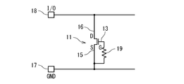
- FIGS. 5A and 5B are circuit diagrams illustrating examples of usage modes of the ESD protection element 11 in the semiconductor device 10.
- the gate electrode 13 of the ESD protection element 11 is commonly connected to the source electrode 15, and the commonly connected gate electrode 13 and the source electrode 15 are connected to the ground pad 17.
- the drain electrode 16 of the ESD protection element 11 is connected to an I / O pad 18 for inputting and outputting signals.
- the ESD protection element 11 functions as a gate-grounded N-channel transistor.
- a resistance element 19 may be connected to the gate electrode 13 as shown in FIG. 5B.
- the resistance element 19 may be realized by a wiring resistance.
- the configuration of the semiconductor device 10 according to the present embodiment described above has various advantages.
- the chip area can be reduced.
- the ESD protection element 11 can be provided above the region where the semiconductor element 2 of the semiconductor substrate 1 is provided, so a dedicated area for providing the ESD protection element 11 is prepared. There is no need. This is effective in reducing the chip area.
- the ESD protection element 11 having the configuration of this embodiment has an advantage that the breakdown voltage can be adjusted in a wide range.
- the breakdown voltage between the gate electrode 13 and the drain electrode 16 can be adjusted over a wide range by appropriately selecting the material and film thickness of the diffusion prevention layer 7-1. Further, as shown in FIGS. 4B and 4C, when the drain electrode 16 does not overlap the gate electrode 13, the breakdown voltage between the gate electrode 13 and the drain electrode 16 is reduced. Can be adjusted by distance.
- the ESD protection element 11 of the present embodiment can be designed as a high breakdown voltage element by adjusting the breakdown voltage.
- the breakdown voltage between the drain electrode 16 and the gate electrode 13 can be increased. 4B, when the drain electrode 16 does not overlap the gate electrode 13, the distance between the drain electrode 16 and the gate electrode 13 is increased to increase the distance between the gate electrode 13 and the drain electrode 16.
- the withstand voltage can be increased.
- the breakdown voltage between the source electrode 15 and the drain electrode 16 can be increased.
- an oxide semiconductor generally has a band gap higher than the band gap of silicon (about 1.2 eV), so that the breakdown voltage between the source electrode 15 and the drain electrode 16 can be obtained by using an oxide semiconductor as the semiconductor layer 12.
- the band gap of InGaZnO (IGZO) is 3.3 to 3.4 eV
- other oxide semiconductors InZnO (IZO), ZnO, ZnAlO, ZnCuO, etc.
- the ESD protection element 11 of the present embodiment having a withstand voltage of 20 to 100 V, which is difficult to realize with a CMOS integrated circuit using a general silicon semiconductor substrate due to its design. Can be realized.
- the semiconductor device 10 of this embodiment has an advantage that the ESD surge does not reach the semiconductor substrate 1.
- the ESD protection element 107 is provided on the semiconductor substrate 101
- a large current is generated.
- the semiconductor substrate 101 There is a possibility of flowing through the semiconductor substrate 101.
- the ESD surge can be released to the ground pad 17 without flowing the current due to the ESD surge to the semiconductor substrate 1, and the semiconductor substrate 1 can be prevented from being thermally destroyed.
- the conventional ESD protection element as shown in FIG. 1 and the ESD protection element 11 of the present embodiment in combination, it is possible to reduce the ESD surge transmitted to the semiconductor substrate. According to such a configuration, the characteristics of the ESD protection element can be improved without increasing the chip area.
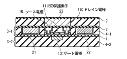
- FIG. 6 is a cross-sectional view showing an example of a configuration in which metal wiring having high thermal conductivity is provided in the vicinity of the ESD protection element 11.
- heat radiation wires 21 and 22 are formed in the same wiring layer 3-1 as the source electrode 15 and the drain electrode 16.
- a heat dissipation wiring 23 is formed in the wiring layer 3 located above the wiring layer 3-1 on which the source electrode 15 and the drain electrode 16 are formed.
- the wirings 21 to 23 may be used also as power supply lines, ground lines, or signal transmission lines, or may be used exclusively for heat dissipation. When the wirings 21 to 23 are used exclusively for heat dissipation, they need not be connected to the other wirings 5 and elements.
- the ESD protection element 11 may be used for protection from an ESD surge in the internal circuit.
- the internal circuit is a circuit using an active element (mainly a MOS transistor) formed on the semiconductor substrate 1 and a circuit using an active element formed in the wiring layer 3 above the semiconductor substrate 1. (Active element using a semiconductor layer formed in the wiring layer 3) or a circuit including both an active element formed in the semiconductor substrate 1 and an active element formed in the wiring layer 3.
- FIG. 12 shows an example of a circuit configuration using the ESD protection element 11 for protecting the internal circuit 203 from an ESD surge.
- the grounding of the ESD protection element 11 and the ground of the internal circuit 203 are separated, the ground pad 201 is connected to the ESD protection element 11, and the ground pad 202 is connected to the internal circuit 203. Yes.
- the grounding of the ESD protection element 11 and the grounding of the internal circuit 203 it is possible to reliably release a large current to the grounding pad 201 connected to the ESD protection element 11.
- FIG. 13 is a cross-sectional view showing an example of the structure of the semiconductor device having the circuit configuration of FIG.
- the I / O pad 18 is connected to both the internal circuit 203 and the ESD protection element 11, but the present invention is not limited to such a configuration.
- an ESD surge 204 enters from the I / O pad 18, a current flows through the ESD protection element 11 formed in the wiring layer 3. That is, the ESD surge 204 can be released to the ground pad 201 connected to the ESD protection element 11 without causing the ESD surge 204 to enter the internal circuit 203 including the semiconductor element 2 formed on the semiconductor substrate 1. Thereby, destruction of the internal circuit 203 can be prevented.
- FIG. 14 shows an example of a circuit configuration of a semiconductor device including both an internal circuit 206 using an active element formed on the semiconductor substrate 1 and an internal circuit 207 using an active element formed on the wiring layer 3.
- the active element formed in the wiring layer 3 refers to an active element formed using a semiconductor layer formed in the wiring layer 3, similarly to the ESD protection element 11.
- the internal circuits 206 and 207 are electrically connected, and an output signal from the active element formed on the semiconductor substrate 1 is input to the active element formed on the wiring layer 3.
- the active elements formed on the semiconductor substrate 1 and the active elements formed on the wiring layer 3 may function separately without being electrically connected.
- I / O pads are prepared for each. May be.
- the I / O pad 18 connected to the internal circuit 206 and the I / O pad 18A connected to the internal circuit 207 are provided separately. It is preferable to connect an ESD protection element to each of the I / O pads 18 and 18A.
- ESD protection elements 11 and 11A are connected to I / O pads 18 and 18A connected to internal circuits 206 and 207, respectively.
- FIG. 15 is a cross-sectional view showing an example of the structure of the semiconductor device having the circuit configuration of FIG.
- an internal circuit 206 using active elements formed on the semiconductor substrate 1 and an internal circuit 207 using active elements formed on the wiring layer 3 are electrically connected.
- ESD protection elements 11 and 11A are provided for protecting the internal circuits 206 and 207, respectively.
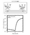
- FIG. 7A is a graph showing an example of characteristics when the ESD protection element 11 performs a transistor operation
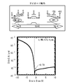
- FIG. 7B is a graph showing an example of characteristics when a diode operation is performed.
- the semiconductor layer 12 is formed of IGZO, and 20 nm of SiN is used as the gate insulating film (diffusion prevention layer 7-1).
- the source potential (the potential of the source electrode 15) is fixed at 0V
- the positive potential bias is applied to the gate electrode 13 while the drain potential Vd (the potential of the drain electrode 16) is fixed at 1V.
- drain current flows while applying a negative voltage bias blocks the drain current. This result means that the ESD protection element 11 actually performs the transistor operation.
- the gate electrode 13 and the source electrode 15 are fixed at 0 V (this means that the ESD protection element 11 is diode-connected), and the drain electrode 16
- the on-voltage is ⁇ 0.7V.
- the ESD protection element 11 actually performs a diode operation (rectification operation).
- the inventor has confirmed through experiments that the ESD protection element 11 provided in the wiring layer 3 actually operates as an active element (transistor or diode).
- the advantage of the ESD protection element 11 of the present embodiment is that a high breakdown voltage characteristic can be realized and the degree of freedom in adjusting the breakdown voltage is great.
- the inventors have actually produced an ESD protection element. 11 has been measured to demonstrate this advantage.
- the configuration of the ESD protection element 11 for which the breakdown voltage was measured is as follows.
- the semiconductor layer 12 is a 10 nm IGZO film, and a 20 to 50 nm SiN film is used as the gate insulating film (diffusion prevention layer 7-1).
- the gate length L and the gate width W are both 0.6 ⁇ m.
- the source electrode 15 and the drain electrode 16 overlap the gate electrode 13, and the overlap lengths d OL1 and d OL2 are 0.16 ⁇ m. As shown in FIG.
- a voltage bias is applied to the drain electrode 16 with the gate electrode 13 and the source electrode 15 connected in common and fixed at 0V.
- the ESD protection element 11 is used as a grounded gate N-channel transistor, the gate electrode 13 and the source electrode 15 are connected in common, so it is technically appropriate to measure the breakdown voltage with such connection.
- FIG. 8B shows a voltage bias (drain potential Vd) applied to the drain electrode 16 when the semiconductor layer 12 is a 10 nm IGZO film and the gate insulating film (diffusion prevention layer 7-1) is a 20 nm SiN film.
- Vd drain potential
- FIG. 8B shows a voltage bias (drain potential Vd) applied to the drain electrode 16 when the semiconductor layer 12 is a 10 nm IGZO film and the gate insulating film (diffusion prevention layer 7-1) is a 20 nm SiN film.
- Vd voltage bias
- FIG. 8C is a graph showing the relationship between the measured breakdown voltage of the ESD protection element 11 and the thickness of the SiN film used as the gate insulating film.
- a gate-drain breakdown voltage of 20 V or more can be realized.
- the gate-drain breakdown voltage can be increased to about 50V.
- the ESD protection element 11 of the present embodiment can realize a high breakdown voltage characteristic and further has a high degree of freedom in adjusting the breakdown voltage.
- the breakdown voltage of the ESD protection element 11 can be increased by further increasing the thickness of the SiN film. However, if the thickness of the SiN film is excessively increased, the current flowing through the ESD protection element 11 is reduced.
- the film thickness is preferably 100 nm or less.
- the breakdown voltage between the gate and the drain can also be increased by separating the gate electrode 13 and the drain electrode 16 in the in-plane direction of the semiconductor layer 12 (that is, the drain electrode 16 is not overlapped with the gate electrode 13).
- the inventor has demonstrated this by measuring the characteristics of the actually produced ESD protection element 11.
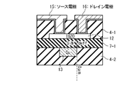
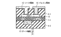
- 9A to 9C are cross-sectional views showing the structure of the fabricated ESD protection element 11. As shown in FIG. In the structure of FIG. 9A, the drain electrode 16 overlaps the gate electrode 13, and in the structure of FIG. 9B, the end of the drain electrode 16 and the end of the gate electrode 13 coincide with each other in the in-plane direction. In the structure of FIG. 9C, the drain electrode 16 does not overlap with the gate electrode 13.
- the distance from the drain electrode 16 to the gate electrode 13 in the in-plane direction is defined as a negative overlap length.
- the semiconductor layer 12 is a 10 nm IGZO film, and a 20 to 50 nm SiN film is used as the gate insulating film (diffusion prevention layer 7-1).
- the gate length L and the gate width W are both 0.6 ⁇ m.
- 10A, 10B, and 10C are graphs of drain current characteristics when the thickness of the SiN film is 20 nm, 30 nm, and 50 nm, respectively.
- the dashed line is when the overlap length is 0.16 ⁇ m
- the broken line is when the overlap length is 0.0 ⁇ m
- the solid line is when the overlap length is ⁇ 0.16 ⁇ m (ie, when there is no overlap) ) Shows the drain current.
- the gate-drain voltage V GD in which the drain current changes suddenly indicates the gate-drain breakdown voltage.
- FIG. 11 is a graph showing the relationship between the overlap length of the drain electrode 16 with respect to the gate electrode 13 and the gate-drain breakdown voltage.
- the structure in which the drain electrode 16 overlaps the gate electrode 13 and the structure in which the end of the drain electrode 16 and the end of the gate electrode 13 coincide in the in-plane direction are The breakdown voltage between the drains does not depend on the overlap length. This is presumably because the distance def (when defined at the shortest position) between the drain electrode 16 and the gate electrode 13 is the same in the film thickness of the diffusion prevention layer 7-1.
- the distance diff between the drain electrode 16 and the gate electrode 13 increases. The increase in the breakdown voltage between the gate and the drain is considered to be caused by the increase in the distance diff.
- FIG. 2 discloses a configuration in which the semiconductor layer 12 is provided on the uppermost wiring layer 3-1, but the semiconductor layer 12 can be provided at an appropriate position as long as it is away from the semiconductor substrate 1. Please note that.
Landscapes
- Semiconductor Integrated Circuits (AREA)
- Metal-Oxide And Bipolar Metal-Oxide Semiconductor Integrated Circuits (AREA)
- Physics & Mathematics (AREA)
- Health & Medical Sciences (AREA)
- Electromagnetism (AREA)
- Toxicology (AREA)
- Internal Circuitry In Semiconductor Integrated Circuit Devices (AREA)
- Thin Film Transistor (AREA)
Abstract
Description
discharge)保護素子を備える半導体装置に関する。
1:半導体基板
2:半導体素子
3:配線層
4:層間絶縁膜
5:配線
6:ビア
7:拡散防止層
8:バリアメタル層
11:ESD保護素子
12:半導体層
13:ゲート電極
14:ハードマスク層
15:ソース電極
16:ドレイン電極
17:接地パッド
18:I/Oパッド
19:抵抗素子
21、22、23:配線
100:半導体装置
101:半導体基板
102:半導体素子
103:配線層
104:配線
105:層間絶縁膜
106:ビア
107:ESD保護素子
108、109:配線
201、202:接地パッド
203:内部回路
204:ESDサージ
206、207:内部回路
Claims (7)
- 半導体素子が形成された半導体基板と、
第1及び第2パッドと、
前記半導体基板の上方に形成された第1絶縁膜と、
前記第1絶縁膜に設けられた溝に埋め込まれた複数の配線と、
前記第1絶縁膜と前記複数の配線とを被覆するように設けられた第2絶縁膜と、
前記第2絶縁膜の上に形成された半導体層と、
前記半導体層に接続されたソース電極と、
前記半導体層に接続されたドレイン電極
とを具備し、
前記複数の配線は、前記半導体層に対向する位置に設けられたゲート電極を含み、
前記半導体層と前記ソース電極と前記ドレイン電極と前記ゲート電極とが、前記第1パッドから前記第2パッドにESDサージによる電流を放電するESD保護素子を構成している
半導体装置。 - 請求項1に記載の半導体装置であって、
前記半導体層は、InGaZnO、InZnO、ZnO、ZnAlO又はZnCuOのいずれかで形成されている
半導体装置。 - 請求項1又は2に記載の半導体装置であって、
前記ドレイン電極が前記半導体層と接触する接触面が前記半導体基板に垂直な方向において前記ゲート電極に重ならない
半導体装置。 - 請求項1乃至3のいずれかに記載の半導体装置であって、
前記ゲート電極と前記ドレイン電極との間の耐圧が20V以上である
半導体装置。 - 請求項4に記載の半導体装置であって、
前記第2絶縁膜がSiN膜である
半導体装置。 - 請求項5に記載の半導体装置であって、
前記第2絶縁膜の膜厚が20nm以上100nm以下である
半導体装置。 - 請求項1乃至6のいずれかに記載の半導体装置であって、
更に、前記ESD保護素子の近傍に設けられた放熱用の配線を備える
半導体装置。
Priority Applications (7)
| Application Number | Priority Date | Filing Date | Title |
|---|---|---|---|
| US14/002,548 US9263399B2 (en) | 2011-03-09 | 2012-03-06 | Semiconductor device with electro-static discharge protection device above semiconductor device area |
| JP2013503558A JP5583266B2 (ja) | 2011-03-09 | 2012-03-06 | 半導体装置 |
| CN201280012204.6A CN103415920B (zh) | 2011-03-09 | 2012-03-06 | 半导体器件 |
| KR1020137023397A KR101862900B1 (ko) | 2011-03-09 | 2012-03-06 | 반도체 장치 |
| TW105116181A TW201631732A (zh) | 2011-03-09 | 2012-03-08 | 半導體裝置 |
| TW101107963A TWI552301B (zh) | 2011-03-09 | 2012-03-08 | 半導體裝置 |
| US14/995,706 US9530769B2 (en) | 2011-03-09 | 2016-01-14 | Semiconductor device with electro-static discharge protection device above semiconductor device area |
Applications Claiming Priority (2)
| Application Number | Priority Date | Filing Date | Title |
|---|---|---|---|
| JP2011-052209 | 2011-03-09 | ||
| JP2011052209 | 2011-03-09 |
Related Child Applications (2)
| Application Number | Title | Priority Date | Filing Date |
|---|---|---|---|
| US14/002,548 A-371-Of-International US9263399B2 (en) | 2011-03-09 | 2012-03-06 | Semiconductor device with electro-static discharge protection device above semiconductor device area |
| US14/995,706 Continuation US9530769B2 (en) | 2011-03-09 | 2016-01-14 | Semiconductor device with electro-static discharge protection device above semiconductor device area |
Publications (1)
| Publication Number | Publication Date |
|---|---|
| WO2012121255A1 true WO2012121255A1 (ja) | 2012-09-13 |
Family
ID=46798212
Family Applications (1)
| Application Number | Title | Priority Date | Filing Date |
|---|---|---|---|
| PCT/JP2012/055707 Ceased WO2012121255A1 (ja) | 2011-03-09 | 2012-03-06 | 半導体装置 |
Country Status (6)
| Country | Link |
|---|---|
| US (2) | US9263399B2 (ja) |
| JP (1) | JP5583266B2 (ja) |
| KR (1) | KR101862900B1 (ja) |
| CN (1) | CN103415920B (ja) |
| TW (2) | TW201631732A (ja) |
| WO (1) | WO2012121255A1 (ja) |
Cited By (7)
| Publication number | Priority date | Publication date | Assignee | Title |
|---|---|---|---|---|
| JP2014075570A (ja) * | 2012-09-14 | 2014-04-24 | Renesas Electronics Corp | 半導体装置、及び半導体装置の製造方法 |
| JP2014187181A (ja) * | 2013-03-22 | 2014-10-02 | Toshiba Corp | 半導体装置及びその製造方法 |
| JP2015046561A (ja) * | 2012-11-28 | 2015-03-12 | 株式会社半導体エネルギー研究所 | 表示装置 |
| JP2017147385A (ja) * | 2016-02-19 | 2017-08-24 | 三菱電機株式会社 | 非線形素子、アレイ基板、およびアレイ基板の製造方法 |
| US10056405B2 (en) | 2015-10-02 | 2018-08-21 | Renesas Electronics Corporation | Semiconductor device and manufacturing method thereof |
| JP7665255B1 (ja) * | 2024-12-27 | 2025-04-21 | Nc技研株式会社 | 半導体装置および電子機器 |
| WO2026074865A1 (ja) * | 2024-10-04 | 2026-04-09 | 株式会社ソシオネクスト | 半導体集積回路装置 |
Families Citing this family (6)
| Publication number | Priority date | Publication date | Assignee | Title |
|---|---|---|---|---|
| KR102078340B1 (ko) * | 2013-07-17 | 2020-02-18 | 삼성디스플레이 주식회사 | 정전기 보호 회로 및 이를 구비한 전자 장치 |
| US10658318B2 (en) | 2016-11-29 | 2020-05-19 | Taiwan Semiconductor Manufacturing Co., Ltd. | Film scheme for bumping |
| CN106783842B (zh) | 2017-01-04 | 2019-05-17 | 京东方科技集团股份有限公司 | 一种静电保护电路、阵列基板、显示面板及显示装置 |
| JP6877261B2 (ja) * | 2017-06-23 | 2021-05-26 | ルネサスエレクトロニクス株式会社 | 半導体装置およびその製造方法 |
| CN114451074B (zh) * | 2019-09-27 | 2023-07-21 | 庆鼎精密电子(淮安)有限公司 | 中介板、中介板的制作方法及电路板组件 |
| JP2024000771A (ja) * | 2022-06-21 | 2024-01-09 | キヤノン株式会社 | 半導体装置、半導体装置の製造方法、機器、基板、基板の製造方法 |
Citations (8)
| Publication number | Priority date | Publication date | Assignee | Title |
|---|---|---|---|---|
| JPS60148161A (ja) * | 1984-01-13 | 1985-08-05 | Hitachi Ltd | 半導体集積回路装置 |
| JPH01295455A (ja) * | 1988-05-24 | 1989-11-29 | Matsushita Electric Ind Co Ltd | 半導体積層集積回路素子 |
| JP2005019452A (ja) * | 2003-06-23 | 2005-01-20 | Toshiba Corp | 半導体装置 |
| JP2008218818A (ja) * | 2007-03-06 | 2008-09-18 | Toshiba Corp | 半導体装置 |
| WO2010030532A1 (en) * | 2008-09-09 | 2010-03-18 | Qualcomm Incorporated | Systems and methods for enabling esd protection on 3-d stacked devices |
| JP2010129958A (ja) * | 2008-12-01 | 2010-06-10 | Seiko Epson Corp | 半導体装置及び半導体装置の製造方法 |
| JP2010141174A (ja) * | 2008-12-12 | 2010-06-24 | Seiko Epson Corp | 半導体装置及び半導体装置の製造方法 |
| JP2010206186A (ja) * | 2009-02-09 | 2010-09-16 | Semiconductor Energy Lab Co Ltd | 保護回路、半導体装置、光電変換装置および電子機器 |
Family Cites Families (9)
| Publication number | Priority date | Publication date | Assignee | Title |
|---|---|---|---|---|
| JP2003133433A (ja) * | 2001-10-25 | 2003-05-09 | Toshiba Corp | 半導体装置およびその製造方法 |
| JP3858883B2 (ja) * | 2003-10-28 | 2006-12-20 | ソニー株式会社 | 記録装置及びその制御方法 |
| EP1624333B1 (en) * | 2004-08-03 | 2017-05-03 | Semiconductor Energy Laboratory Co., Ltd. | Display device, manufacturing method thereof, and television set |
| JP5116277B2 (ja) * | 2006-09-29 | 2013-01-09 | 株式会社半導体エネルギー研究所 | 半導体装置、表示装置、液晶表示装置、表示モジュール及び電子機器 |
| KR100788589B1 (ko) * | 2007-01-19 | 2007-12-26 | 삼성에스디아이 주식회사 | 유기 전계 발광 표시 장치 |
| JP5540517B2 (ja) | 2008-02-22 | 2014-07-02 | 凸版印刷株式会社 | 画像表示装置 |
| KR101533391B1 (ko) | 2008-08-06 | 2015-07-02 | 삼성디스플레이 주식회사 | 박막 트랜지스터 기판과 그 제조 방법 |
| KR101634411B1 (ko) | 2008-10-31 | 2016-06-28 | 가부시키가이샤 한도오따이 에네루기 켄큐쇼 | 구동 회로, 표시 장치 및 전자 장치 |
| JP5781720B2 (ja) | 2008-12-15 | 2015-09-24 | ルネサスエレクトロニクス株式会社 | 半導体装置及び半導体装置の製造方法 |
-
2012
- 2012-03-06 WO PCT/JP2012/055707 patent/WO2012121255A1/ja not_active Ceased
- 2012-03-06 JP JP2013503558A patent/JP5583266B2/ja not_active Expired - Fee Related
- 2012-03-06 CN CN201280012204.6A patent/CN103415920B/zh not_active Expired - Fee Related
- 2012-03-06 KR KR1020137023397A patent/KR101862900B1/ko not_active Expired - Fee Related
- 2012-03-06 US US14/002,548 patent/US9263399B2/en active Active
- 2012-03-08 TW TW105116181A patent/TW201631732A/zh unknown
- 2012-03-08 TW TW101107963A patent/TWI552301B/zh not_active IP Right Cessation
-
2016
- 2016-01-14 US US14/995,706 patent/US9530769B2/en not_active Expired - Fee Related
Patent Citations (8)
| Publication number | Priority date | Publication date | Assignee | Title |
|---|---|---|---|---|
| JPS60148161A (ja) * | 1984-01-13 | 1985-08-05 | Hitachi Ltd | 半導体集積回路装置 |
| JPH01295455A (ja) * | 1988-05-24 | 1989-11-29 | Matsushita Electric Ind Co Ltd | 半導体積層集積回路素子 |
| JP2005019452A (ja) * | 2003-06-23 | 2005-01-20 | Toshiba Corp | 半導体装置 |
| JP2008218818A (ja) * | 2007-03-06 | 2008-09-18 | Toshiba Corp | 半導体装置 |
| WO2010030532A1 (en) * | 2008-09-09 | 2010-03-18 | Qualcomm Incorporated | Systems and methods for enabling esd protection on 3-d stacked devices |
| JP2010129958A (ja) * | 2008-12-01 | 2010-06-10 | Seiko Epson Corp | 半導体装置及び半導体装置の製造方法 |
| JP2010141174A (ja) * | 2008-12-12 | 2010-06-24 | Seiko Epson Corp | 半導体装置及び半導体装置の製造方法 |
| JP2010206186A (ja) * | 2009-02-09 | 2010-09-16 | Semiconductor Energy Lab Co Ltd | 保護回路、半導体装置、光電変換装置および電子機器 |
Cited By (15)
| Publication number | Priority date | Publication date | Assignee | Title |
|---|---|---|---|---|
| JP2014075570A (ja) * | 2012-09-14 | 2014-04-24 | Renesas Electronics Corp | 半導体装置、及び半導体装置の製造方法 |
| JP2025061127A (ja) * | 2012-11-28 | 2025-04-10 | 株式会社半導体エネルギー研究所 | 表示装置 |
| JP7375142B2 (ja) | 2012-11-28 | 2023-11-07 | 株式会社半導体エネルギー研究所 | 半導体装置 |
| JP2025134989A (ja) * | 2012-11-28 | 2025-09-17 | 株式会社半導体エネルギー研究所 | 表示装置 |
| JP7735609B1 (ja) | 2012-11-28 | 2025-09-08 | 株式会社半導体エネルギー研究所 | 表示装置 |
| JP2019185054A (ja) * | 2012-11-28 | 2019-10-24 | 株式会社半導体エネルギー研究所 | 表示装置 |
| JP2021076860A (ja) * | 2012-11-28 | 2021-05-20 | 株式会社半導体エネルギー研究所 | 半導体装置 |
| JP2022183150A (ja) * | 2012-11-28 | 2022-12-08 | 株式会社半導体エネルギー研究所 | 半導体装置 |
| JP2015046561A (ja) * | 2012-11-28 | 2015-03-12 | 株式会社半導体エネルギー研究所 | 表示装置 |
| JP7707460B2 (ja) | 2012-11-28 | 2025-07-14 | 株式会社半導体エネルギー研究所 | 表示装置 |
| JP2014187181A (ja) * | 2013-03-22 | 2014-10-02 | Toshiba Corp | 半導体装置及びその製造方法 |
| US10056405B2 (en) | 2015-10-02 | 2018-08-21 | Renesas Electronics Corporation | Semiconductor device and manufacturing method thereof |
| JP2017147385A (ja) * | 2016-02-19 | 2017-08-24 | 三菱電機株式会社 | 非線形素子、アレイ基板、およびアレイ基板の製造方法 |
| WO2026074865A1 (ja) * | 2024-10-04 | 2026-04-09 | 株式会社ソシオネクスト | 半導体集積回路装置 |
| JP7665255B1 (ja) * | 2024-12-27 | 2025-04-21 | Nc技研株式会社 | 半導体装置および電子機器 |
Also Published As
| Publication number | Publication date |
|---|---|
| TW201301475A (zh) | 2013-01-01 |
| JP5583266B2 (ja) | 2014-09-03 |
| CN103415920A (zh) | 2013-11-27 |
| KR20140047587A (ko) | 2014-04-22 |
| TWI552301B (zh) | 2016-10-01 |
| US20130334529A1 (en) | 2013-12-19 |
| CN103415920B (zh) | 2016-11-09 |
| TW201631732A (zh) | 2016-09-01 |
| US9530769B2 (en) | 2016-12-27 |
| US20160172354A1 (en) | 2016-06-16 |
| US9263399B2 (en) | 2016-02-16 |
| KR101862900B1 (ko) | 2018-05-30 |
| JPWO2012121255A1 (ja) | 2014-07-17 |
Similar Documents
| Publication | Publication Date | Title |
|---|---|---|
| JP5583266B2 (ja) | 半導体装置 | |
| CN101047177B (zh) | 半导体装置 | |
| JP5731904B2 (ja) | 半導体装置及び半導体装置の製造方法 | |
| CN104979342B (zh) | 具有静电放电保护结构的半导体器件 | |
| KR20090020528A (ko) | 반도체 디바이스 | |
| JP2005019452A (ja) | 半導体装置 | |
| JP6841161B2 (ja) | 半導体装置 | |
| US20080135940A1 (en) | Semiconductor Device | |
| JP3729082B2 (ja) | 半導体保護回路 | |
| TWI697092B (zh) | 半導體靜電放電保護電路、半導體靜電放電保護元件及其佈局結構 | |
| US9472544B2 (en) | Semiconductor device comprising electrostatic discharge protection structure | |
| JP4995364B2 (ja) | 半導体集積回路装置 | |
| US8710589B2 (en) | Semiconductor device | |
| JP6100026B2 (ja) | 半導体装置 | |
| JP7052972B2 (ja) | 半導体集積回路 | |
| TWI575698B (zh) | 半導體裝置 | |
| JP2006261154A (ja) | 半導体装置およびその設計方法 | |
| WO2021205879A1 (ja) | 半導体装置 | |
| JP2009141258A (ja) | 半導体装置 | |
| JP2013149671A (ja) | 半導体装置 | |
| JPH0777235B2 (ja) | 半導体入力保護装置 |
Legal Events
| Date | Code | Title | Description |
|---|---|---|---|
| 121 | Ep: the epo has been informed by wipo that ep was designated in this application |
Ref document number: 12755680 Country of ref document: EP Kind code of ref document: A1 |
|
| ENP | Entry into the national phase |
Ref document number: 2013503558 Country of ref document: JP Kind code of ref document: A |
|
| WWE | Wipo information: entry into national phase |
Ref document number: 14002548 Country of ref document: US |
|
| ENP | Entry into the national phase |
Ref document number: 20137023397 Country of ref document: KR Kind code of ref document: A |
|
| NENP | Non-entry into the national phase |
Ref country code: DE |
|
| 122 | Ep: pct application non-entry in european phase |
Ref document number: 12755680 Country of ref document: EP Kind code of ref document: A1 |