WO2012120919A1 - プラズマ分光分析装置 - Google Patents
プラズマ分光分析装置 Download PDFInfo
- Publication number
- WO2012120919A1 WO2012120919A1 PCT/JP2012/050552 JP2012050552W WO2012120919A1 WO 2012120919 A1 WO2012120919 A1 WO 2012120919A1 JP 2012050552 W JP2012050552 W JP 2012050552W WO 2012120919 A1 WO2012120919 A1 WO 2012120919A1
- Authority
- WO
- WIPO (PCT)
- Prior art keywords
- plasma
- measurement
- light emission
- emission
- narrow portion
- Prior art date
- Legal status (The legal status is an assumption and is not a legal conclusion. Google has not performed a legal analysis and makes no representation as to the accuracy of the status listed.)
- Ceased
Links
Images


Classifications
-
- G—PHYSICS
- G01—MEASURING; TESTING
- G01N—INVESTIGATING OR ANALYSING MATERIALS BY DETERMINING THEIR CHEMICAL OR PHYSICAL PROPERTIES
- G01N21/00—Investigating or analysing materials by the use of optical means, i.e. using sub-millimetre waves, infrared, visible or ultraviolet light
- G01N21/62—Systems in which the material investigated is excited whereby it emits light or causes a change in wavelength of the incident light
- G01N21/66—Systems in which the material investigated is excited whereby it emits light or causes a change in wavelength of the incident light electrically excited, e.g. electroluminescence
- G01N21/67—Systems in which the material investigated is excited whereby it emits light or causes a change in wavelength of the incident light electrically excited, e.g. electroluminescence using electric arcs or discharges
-
- G—PHYSICS
- G01—MEASURING; TESTING
- G01N—INVESTIGATING OR ANALYSING MATERIALS BY DETERMINING THEIR CHEMICAL OR PHYSICAL PROPERTIES
- G01N21/00—Investigating or analysing materials by the use of optical means, i.e. using sub-millimetre waves, infrared, visible or ultraviolet light
- G01N21/62—Systems in which the material investigated is excited whereby it emits light or causes a change in wavelength of the incident light
- G01N21/66—Systems in which the material investigated is excited whereby it emits light or causes a change in wavelength of the incident light electrically excited, e.g. electroluminescence
- G01N21/69—Systems in which the material investigated is excited whereby it emits light or causes a change in wavelength of the incident light electrically excited, e.g. electroluminescence specially adapted for fluids, e.g. molten metal
-
- G—PHYSICS
- G01—MEASURING; TESTING
- G01J—MEASUREMENT OF INTENSITY, VELOCITY, SPECTRAL CONTENT, POLARISATION, PHASE OR PULSE CHARACTERISTICS OF INFRARED, VISIBLE OR ULTRAVIOLET LIGHT; COLORIMETRY; RADIATION PYROMETRY
- G01J3/00—Spectrometry; Spectrophotometry; Monochromators; Measuring colours
- G01J3/02—Details
-
- G—PHYSICS
- G01—MEASURING; TESTING
- G01N—INVESTIGATING OR ANALYSING MATERIALS BY DETERMINING THEIR CHEMICAL OR PHYSICAL PROPERTIES
- G01N2201/00—Features of devices classified in G01N21/00
- G01N2201/08—Optical fibres; light guides
Definitions
- the present invention relates to a plasma spectroscopic analyzer for analyzing a liquid sample using plasma emission.
- Patent Document 1 There is Japanese Patent No. 3932368 (Patent Document 1) as background art of the present invention.
- Patent Document 1 a narrow portion having a cross-sectional area that is significantly smaller than the cross-sectional area of the flow channel is provided in the flow channel formed of an insulating material, and after the conductive liquid is filled in the flow channel and the narrow portion, the narrow portion is Describes a plasma generation method and an elemental analysis method in which an electric field is applied to a narrow portion so that an electric field passes through and a plasma is generated in the narrow portion.
- a narrow portion having a cross-sectional area that is significantly smaller than the cross-sectional area of the flow channel is disposed in the flow channel formed of an insulating material, and an electric field is applied to the narrow portion so that the electric field passes through the narrow portion.
- Patent Document 1 describes that bubbles are generated in a narrow portion and plasma is generated in the generated bubbles. Further, there is a description that when the generated plasma develops larger than the volume in the narrowed portion of the flow path, the shape and brightness of the plasma changes drastically, and thus the emission intensity varies greatly. However, by developing bubbles much larger than the size of the narrow part and developing plasma much larger, it is possible to generate phenomena that have not been known so far, and to improve detection sensitivity, detection accuracy, and reproducibility. Not listed.
- Patent Document 1 describes that an accurate measurement can be performed by adjusting the electrical conductivity of a specimen to an electrical conductivity convenient for plasma generation and measurement. However, there is no description about measuring the time change of the current at the time of voltage application or improving the detection sensitivity, detection accuracy, and reproducibility using the information of the time change of the current.
- the present invention improves detection sensitivity, detection accuracy, and reproducibility in a method in which discharge is generated in a sample solution and analysis is performed using light emission in the plasma.
- the present invention includes a plurality of means for solving the above problems.
- the channel having the narrow portion is filled with a conductive liquid, and an electric field is applied to the channel to generate bubbles.
- a spectroscopic analysis device that generates plasma in bubbles, and a region other than a narrow portion in a flow path is set as a measurement target region.
- Another example is a spectroscopic analyzer that fills a flow path with a conductive liquid, applies an electric field to the flow path to generate bubbles, and generates plasma in the bubbles.
- a specific one-time light emission after the second time or a specific multiple-time light emission is measured.
- Another example is a spectroscopic analyzer that fills a flow path with a conductive liquid, applies an electric field to the flow path to generate bubbles, and generates plasma in the bubbles.
- the timing of the measurement of light emission is controlled using the time change.
- the present invention it is possible to improve detection sensitivity, detection accuracy, and reproducibility in a method in which discharge is generated in a sample solution and analysis is performed using light emission in the plasma.
- bubbles are developed much larger than the size of the narrow portion, and plasma is developed much larger than the narrow portion.
- detection sensitivity can be improved by setting a region other than the narrow portion of the flow channel as a measurement target.
- by developing bubbles much larger than the size of the narrow portion and developing the plasma much larger than the narrow portion measurement can be performed while avoiding the narrow portion.
- the size of the bubble and plasma varies depending on the shape of the flow path, the arrangement of the electrodes, the composition of the sample solution, etc. in addition to the magnitude of the applied voltage and the voltage application time, so it is difficult to specify the generation conditions in general.
- the applied voltage is preferably 500 V or higher, more preferably 1 kV or higher, more preferably about 1.5 kV or higher, and still more preferably 2.5 kV or higher.
- the voltage application time is desirably 0.1 milliseconds or more, more desirably 0.2 milliseconds or more, more desirably 0.5 milliseconds or more, and further desirably 0.8 milliseconds or more.
- the sample solution needs to be electrically conductive, and an acid generally used in elemental analysis, such as nitric acid, is suitable.
- an acid generally used in elemental analysis such as nitric acid
- various acids such as hydrochloric acid and sulfuric acid can be used, and a solution containing salts having electrical conductivity can also be used.
- the appropriate region to be measured is within the range where bubbles and plasma exist, and since it depends on the size of the bubbles and plasma, it is difficult to specify in general, but the length b in the voltage application direction of the narrow portion is set. Taking the standard, it is considered as follows.
- the distance between the center of the narrow part and the center of the region to be measured is preferably about 5 times or more, more preferably about 3 times or more, more preferably about 2 times or more, more preferably about 1 time compared to b. That's it. Since light emission occurs in the range where bubbles and plasma exist, the range of the channel farthest from the center of the narrow portion is appropriate as the measurement target region.
- the conditions for generating light emission multiple times for a single voltage application vary depending on the shape of the flow path, electrode arrangement, and sample solution composition, as well as the applied voltage and voltage application time. Is difficult to specify, but is almost equivalent to the condition that bubbles and plasma are sufficiently larger than the size of the narrow portion.
- the voltage applied to the flow path across the narrow portion is preferably 500 V or higher, more preferably 1 kV or higher, more preferably about 1.5 kV or higher, more preferably 2.5 kV or higher.
- the voltage application time is desirably 0.5 milliseconds or more, and more desirably 0.8 milliseconds or more.
- One method is a method in which the timing of exposure is controlled to measure all light emissions in an appropriate time interval.
- the present invention can be applied to the case where light emission is detected using a CCD camera as a detection element.
- the time change of current is measured at the same time, and when the current value satisfies a preset condition, an exposure signal is transmitted to the detector to measure light emission.
- the time change of the current is measured in advance under the same conditions, the exposure timing is determined in advance from the recorded time change of the current, and this exposure timing is used. It is also possible to measure luminescence.
- Another method is to record all the time variation of light emission in a storage device such as a memory and read the light emission amount in an appropriate time interval from the recorded time variation of light emission after voltage application is completed, or
- the present invention can be applied to the case where light emission is detected using a photomultiplier tube as a detection element.
- the time change of the current is recorded in a storage device such as a memory at the same time, and after the voltage application is finished, the light emission data is processed using the time change of the recorded current.
- the time change of the current is measured in advance under the same conditions, and the time division for reading or integrating the light emission data can be determined from the recorded time change of the current.
- the time change of the current when the electric field is applied to the sample solution containing the analyte is measured, and then the time change of the current when the electric field of the reference solution is applied matches the time change of the current of the sample solution. It is also possible to estimate the amount of the substance to be analyzed in the sample solution with reference to the measured reference light intensity by applying a voltage to the adjusted reference solution and measuring the luminescence.
- the main composition of the sample solution When the main composition of the sample solution is known, it is desirable to use a seed solution that constitutes the main composition as the reference solution.
- the type of acid when the type of acid is known, it is desirable to use the same type of acid.
- Nitric acid is often used for elemental analysis, so it is often appropriate to use nitric acid. It is also appropriate to use other acids such as hydrochloric acid and sulfuric acid.
- the electrical conductivity of the sample solution is derived from a salt that is mainly dissolved, it is appropriate to use a solution containing the same type of salt, and examples include sodium chloride and potassium chloride.
- the sample solution contains an organic solvent, it is also appropriate to use a preparation solution containing the organic solvent. Examples include ethanol and acetone.
- the above adjustment means for example, when nitric acid is used, by measuring the time change of the current when applying a voltage to a solution in which the mixing ratio of concentrated nitric acid and water is changed little by little, and applying the voltage to the sample solution Select the solution that is closest to the time change of the current over time, or create a solution with a different mixing ratio in order to make the current time changes closer to each other.
- this kind of concentrated solution is adjusted by changing the mixing ratio of water so that the time change of the solution current is close to the time change of the sample solution.
- it is easy to use water in the combination of what to mix it is not limited to it, You may combine 3 or more types of solutions.
- an element to be analyzed is contained in a sample solution at a low concentration that cannot be analyzed conventionally, it can be detected and accurately quantified.
- a sample solution in which the concentration of an element to be analyzed cannot be detected because the concentration of an element to be analyzed is too low unless the concentration step is performed before the analysis is conventionally performed without the concentration step.
- analysis can be performed on an analysis target for which it is not appropriate to perform the concentration step.
- the concentration of the element to be analyzed becomes thin and cannot be detected. Therefore, even after diluting the sample solution, analysis is performed after dilution. Can do.
- since the reproducibility of detection is poor in the past, even a sample solution that had to be analyzed a plurality of times is more reliable with a smaller number of analyzes including one time. The result can be obtained.
- Example 1 In this embodiment, a configuration example of a plasma emission analyzer is described, and a light emission phenomenon caused by discharge of a sample solution is described, and new knowledge that has led to the present invention is described.
- FIG. 1 is a schematic diagram showing a configuration example of the plasma emission spectroscopic apparatus of the present embodiment.
- the flow channel 101 is formed in the quartz glass 102, and the solution can flow through the flow channel 101 through the through holes 103 located upstream and downstream.
- the connectors 105 and 110 press the O-ring 104 against the quartz glass 102 to prevent liquid leakage when the solution flows from the outside to the channel 101.
- Electrodes 107 and 112 are attached to the connectors 105 and 110, respectively, and a voltage can be applied to the solution in the channel 101.
- platinum wires having a diameter of 0.5 mm were used as the electrodes 107 and 112.
- the connectors 105 and 110 are provided with pipe connection ports 106 and 111.
- a pipe 108 is connected to the pipe connection port 106 of the connector 105, and a syringe pump 109 is connected to the pipe 108.
- the syringe pump 109 is connected to the computer 122 via the signal line 119, and the operation is controlled by the computer 122.
- a pipe 113 is connected to the pipe connection port 111 of the other connector 110, and a waste liquid container 114 is installed at the end of the pipe 113.
- the electrodes 107 and 112 are connected to a power source 116 via high-voltage wires 113 and 114, respectively.
- a DC pulse power source is used as the power source 116.
- An ammeter 115 for measuring current is connected in series in the middle of the high-voltage wire 113.
- the computer 122 is connected to the power supply 116 via the signal line 117. Based on the input information, the computer 122 can set the output voltage of the power supply 116 and perform on / off timing control using a trigger.
- the computer 122 is connected to the ammeter 115 via the signal line 118, and can capture measurement data of the ammeter 115, process the measurement data, and use it for controlling the power source 116.
- the camera 121 is connected to the computer 122 via the signal line 120.
- the computer 122 reflects the input camera setting information in the setting of the camera 121, and an image captured by the camera 121 is recorded in the computer 122 and processed. Further, the computer 122 outputs an exposure control signal for the camera 121, and the camera 121 operates by receiving the exposure control signal.
- Light emitted in the channel 101 is captured by the camera 121 through the lenses 123 and 124.
- an image corresponding to the transmission characteristics of the optical filter 125 can be acquired by installing the optical filter 125. It is important to install the lens 123 on the opposite side of the connectors 105 and 110 with respect to the channel 101 so that the entire channel can be photographed without being shaded by the connectors 105 and 110. Since the size of the bubble and plasma related to light emission is large, if the image is taken from the side of the connector, the periphery of the connector is behind the connector and cannot be imaged.
- the data related to light emission which is captured by the camera 121 and recorded in the memory of the computer 122, is combined with the data related to the temporal change of the current measured by the ammeter 115 and recorded in the memory of the computer 122.
- Information processing can also be performed.
- the computer 122 performs the function as the control unit and the function as the calculation unit simultaneously.
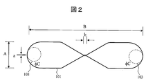
- FIG. 2 is a diagram for explaining an example of the flow path 101 used in the present embodiment.
- the channel 101 is a channel having a uniform depth, having a width A and a total length B, a narrow portion having a width a and a length b at the center.
- the width a of the narrow portion is narrower than the width A of the flow path, preferably 1/3 or less of the width A of the flow path, more preferably 1/10 or less.
- the length b of the narrow portion is shorter than the full length B, preferably 1/5 or less of the full length B, more preferably 1/10 or less.
- the total length B of the flow path is preferably 1 mm or more and 30 cm or less.
- the depth of the flow path is approximately the same as the width of the narrow portion or less than or equal to the length of the narrow portion.
- the channel width A is 3 mm
- the channel total length B is 13 mm
- the narrow portion width a is 0.10 mm
- the narrow portion length b is 0.40 mm
- the channel depth is It was set to 0.08 mm.
- the positions of the through holes 103 on the left and right of the channel 101 are indicated by broken lines.
- the diameter of the through hole 103 is approximately the same as the diameter of the hole inside the connector.
- Water was first flowed into the empty flow path 101, and then 0.1 N nitric acid was flowed and washed.
- water is poured into the syringe of the syringe pump 109, and the syringe pump 109 is moved according to an instruction from the computer 122, so that the flow path 101 passes through the pipe 108, the pipe connection port 106, the inside of the connector 105, and the through hole 103.
- Water was poured and washed, and the washed water was collected in the waste liquid container 114 through the downstream through hole 103, the inside of the connector 110, the pipe connection port 111, and the pipe 113.
- 0.1 N nitric acid was flowed in the same procedure, and the flow path 101 was washed.
- An appropriate applied voltage is preferably 500 V or more, more preferably 1 kV or more, further preferably about 1.5 kV or more, and further preferably 2.5 kV or more.
- the applied voltage was 2.5 kV
- the voltage applied pulse width was 0.8 milliseconds or 1.8 milliseconds.
- the polarity of the power source 116 was set so that a positive high voltage was applied to the high voltage electric wire 114 side and the high voltage electric wire 113 side was grounded.
- the polarities of the electrodes were set so that the electrode 107 on the upstream side of the sample solution was a negative electrode and the electrode 112 on the downstream side of the sample solution was a positive electrode.
- the relationship between the polarity of the electrode and the flow direction of the sample solution is not limited to this combination, and may be a reverse combination.
- the computer 122 generates a voltage application start signal.
- the power supply 116 receives a signal from the computer 122 and applies a voltage to the channel 101 in accordance with the signal.
- the exposure control of the camera 121 was performed by inputting a signal similar to the voltage application signal from the computer 122 to the camera 121.
- the current measurement by the ammeter 115 was performed by outputting a signal synchronized with the voltage application start signal to the power supply 116 from the computer 122 and inputting it as a signal to the ammeter 115.
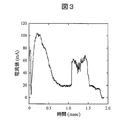
- FIG. 3 is a diagram showing the time change of the current measured by the ammeter 115 in the present embodiment.
- the vertical axis represents current
- the horizontal axis represents time
- the voltage application start time was set to time zero.
- the voltage application pulse width is 1.8 milliseconds.
- a current peak with a maximum value of about 80 milliamperes a current peak in the vicinity of 0.05 milliseconds, and a gentle peak up to 0.8 milliseconds after voltage application, and a voltage peak of 0.
- Three peaks were observed, current peaks with sharp rises after 8 milliseconds.
- the peak of the current immediately after voltage application increases the electric resistance due to the generation of bubbles due to Joule heat from the increase in current due to voltage application, and the current value increases. It corresponds until it decreases, and at this time, light emission is hardly observed. Therefore, except for the peak of the current value immediately after the voltage application, the peak of the current is counted in order, and the number of times of light emission is counted in that order.
- the light emission corresponding to the peak up to 0.8 milliseconds after the voltage application is performed for the first time, and after the voltage application, 0.8 milliseconds and after. Light emission corresponding to the peak up to milliseconds is referred to as second light emission.
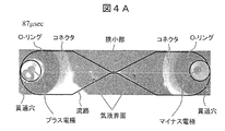
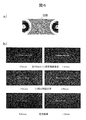
- FIG. 4A to FIG. 4J are examples of images taken with a high-speed camera in the present embodiment and showing the state of bubbles and light emission generated when a voltage is applied.
- the captured images are shown in order of time from the start of voltage application.
- the time described in the upper left of each figure shows the elapsed time from the start of voltage application.
- a high-speed camera is used as the camera 121 shown in FIG. 1 and is taken simultaneously with the measurement of the time change of the current shown in FIG. At the time of photographing, illumination was performed to make the flow path easier to see, and the optical filter 125 was not used.
- FIG. 4A is a photographed image 87 microseconds after voltage application with a description added.
- In the through hole there is a platinum wire having a diameter of 0.5 mm which is an electrode.
- the right electrode is a minus electrode and the left electrode is a plus electrode.
- the sample solution flows from the right to the left in the figure. Since the image is taken from the opposite side of the connector with respect to the flow channel, the inside of the flow channel can be observed without being obstructed by the O-ring and the connector in the figure.
- the channel before the voltage application is filled with the sample solution and, of course, there is no gas-liquid interface.
- the gas channel is almost symmetrically positioned from the narrow part of the channel.
- the liquid interface can be observed. This indicates that the bubbles generated in the narrow portion are spread almost evenly on the left and right, and the narrow portion side of the gas-liquid interface is the bubble, and both electrode sides of the gas-liquid interface are the sample solution.
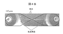
- FIG. 4B is an image added with an explanation after 187 microseconds after voltage application. Bubbles are much larger than the narrow part of the flow path, and the gas-liquid interface can be observed far away from the narrow part and in the vicinity of the connector. Moreover, the linear light emission which spreads right and left through the narrow part can be seen. In this figure, the light emission appears to be linear from the narrow part to the right, almost horizontally, and slightly to the left toward the left. The position of light emission that looks linear is slightly different for each voltage application pulse, but is almost in the vicinity of the line connecting the narrow portion and both electrodes. This light emission is caused by plasma. From this figure, it can be seen that under these conditions, bubbles, light emission, and plasma are present in a much larger region than the narrow portion.
- FIG. 4C shows an image added 337 microseconds after voltage application.
- the bubble is the largest at this timing, and the white line in the figure showing light emission is photographed most intensely.
- the gas-liquid interface is at a position of about 4 mm as measured from the center of the narrow portion, and is about 10 times the distance of the narrow portion having a length of 0.4 mm. It is around this timing that the first light emission has the highest light emission intensity, and the light emission is clearly not limited to the narrow portion, but has a size that protrudes greatly from the narrow portion.
- the light emission can be observed up to about 3 mm away from the center of the narrow portion, and the light emission can be observed up to about 8 times the distance of the narrow portion length of 0.4 mm.
- the bubbles grow large in a symmetrical manner over time, and have a size that protrudes far from the narrow portion. From the fact that the bubbles expand, it can be seen that the pressure inside the bubbles is higher than 1 atm.
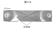
- FIG. 4D is an image after 612 microseconds after voltage application
- FIG. 4E is an image after 837 microseconds after voltage application, with a description added to each. From FIG. 4D to FIG. 4E, it can be seen that the bubbles are shrunk and the emission intensity is reduced. In particular, at the timing of FIG. 4E, a clear light emission line cannot be confirmed. The light that appears strong in the narrow portion is due to the light scattered by the glass in the narrow portion, and is not mainly caused by light emission. As shown in FIG. 3, this timing corresponds to a region where the current value corresponding to the first light emission has substantially decreased.
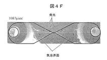
- FIG. 4F shows an image added 1087 microseconds after voltage application.
- FIG. 4F captures the timing at which the second light emission starts.
- the gas-liquid interface on the positive pole side on the left when viewed from the narrow part has a convex shape facing the right, and the tip of the convex part and the gas-liquid interface on the negative pole side on the right when viewed from the narrow part Discharge occurs between them, and light is emitted.
- the position of the gas-liquid interface is about 2 mm from the center of the narrow portion, and is about five times as long as the length of the narrow portion is 0.4 mm.
- the current increases rapidly at the start of the second light emission.
- the distance between the left and right gas-liquid interfaces at the timing when the second light emission started was an average of 4.5 mm.
- Paschen's law holds between the product of the discharge start voltage V, the material pressure p, and the discharge distance d, and has a Paschen curve specific to the material.
- the internal pressure of the bubbles is about 0.1 atm and the pressure is reduced.
- FIG. 4G is an image after 1237 microseconds after voltage application
- FIG. 4H is an image after 1387 microseconds after voltage application, with a description added to each.
- 4G and 4H are images during the second light emission, and change to a shape in which the tip of the convex portion of the gas-liquid interface on the positive pole side, which is on the left when viewed from the narrow portion, is pushed little by little. And that the position does not move too much.
- the gas-liquid interface on the negative pole side on the right when viewed from the narrow part changes greatly during the second light emission, and it can be seen that it is blown away.
- the gas-liquid interface on either side is away from the narrow portion and moves in the direction in which the bubbles increase.
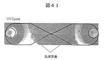
- FIG. 4I is an image added with a description after 1512 microseconds after voltage application.
- FIG. 4I captures the timing at which the second light emission is stopped. As can be seen from FIG. 3, the current rapidly decreases at the timing of the second light emission stop. It is considered that the distance between the gas-liquid interface is increased by the discharge, and the voltage necessary for the discharge is not sufficient for the distance, the discharge is stopped, and the light emission is stopped.
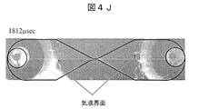
- FIG. 4J is an image added with an explanation after 1812 microseconds after voltage application.
- FIG. 4J is an image immediately after the voltage application is stopped. Following FIG. 4I, no luminescence is observed.
- FIG. 5 is a diagram for explaining the change over time of the position of the gas-liquid interface and the distance between the gas-liquid interface. It was created using the same imaging data as in FIGS. 4A to 4J.
- the position of the gas-liquid interface is the absolute value measured with the center of the narrow part as the origin for both the left (plus pole side) and right (minus pole side) gas-liquid interface, and the distance between the gas-liquid interface Corresponds to the sum of the positions of the left and right gas-liquid interfaces.
- the position of the gas-liquid interface is about 4 mm or more from the center of the narrow part. Moreover, it turns out that the distance between gas-liquid interfaces spreads to about 8 mm. Both are much larger areas than the size of the narrow part. If the length of the narrow portion is taken to be the representative size of the narrow portion, the distance increases from the center of the local minimum portion to about 10 times the distance of the narrow portion, and the size of the bubble is about 20 times larger. I understand that.
- the speed at which the bubbles spread is as high as about 100 km / h when calculated from the relationship between the position of the gas-liquid interface and time.
- the gas-liquid interface position on the positive electrode side is about 2 mm, and then the bubbles become larger. Even at this point, the bubbles are spread over a much larger area than the narrow portion. Assuming that the narrow portion length of 0.4 mm is the representative size of the narrow portion, it can be seen that the narrow portion extends from the center of the narrow portion to about five times the narrow portion.
- FIG. 6 is a diagram for explaining an example of the light emission distribution observed in this example. Images were taken using a cooled CCD camera as the camera 121 shown in FIG. As the optical filter 125, a band pass filter having a center wavelength of 405 nm and a half width of 10 nm was used. Since the neutral atom (PbI) of lead has an emission line at a wavelength of 405.78 nm, the atomic emission of lead can be observed through this optical filter.
- PbI neutral atom
- FIG. 6A is an explanatory diagram showing the position of the flow path in the figure, and the image is obtained by removing the optical filter 125 from the configuration shown in FIG. 1 and illuminating the entire flow path with illumination. The outer edge of is written.
- FIG. 6B shows a light emission distribution. Each image in FIGS. 6A and 6B is displayed at the same scale, and the position in the figure is common to each image. Two samples, a 0.1 N nitric acid solution containing 100 ppm lead and a 0.1 N nitric acid solution, were used as sample solutions, and light emission images were obtained under the conditions of a voltage application pulse width of 0.8 milliseconds and 1.8 milliseconds. Was taken.
- FIG. 1 An image obtained by averaging the luminescence images for 96 pulses is shown in FIG. The following analysis was performed using this image. Moreover, it corresponds to a 0.1 N nitric acid solution from an image corresponding to a 0.1 N nitric acid solution containing 100 ppm of lead under each condition of a voltage application pulse width of 0.8 msec and 1.8 msec. A difference image was created by subtracting the images and displayed together.
- luminescence is observed in the region where the narrow portion of the flow path shown in FIG. 6A is greatly protruded from all the images showing the light emission distribution shown in FIG.
- light emission can be observed up to about 3 mm away from the center of the narrow portion, and it can be seen that light is emitted in a much larger region than the narrow portion.
- the length of the narrow portion is 0.4 mm and the typical size of the narrow portion is taken, it can be seen that light emission can be observed from the center of the narrow portion to a distance of about 8 times the size of the narrow portion. Since this light emission is caused by plasma, the magnitude of the plasma may be considered the same.
- a light emission distribution centered on the narrow part of the flow path can be seen for any solution.
- the 0.1N nitric acid solution does not contain lead, and no emission line having a wavelength that passes through this optical filter is emitted from a separately acquired spectrum.
- the emitted light is considered to be other background light, not atomic emission.
- the emission intensity from a 0.1 N nitric acid solution containing 100 ppm lead is greater than the emission intensity from a 0.1 N nitric acid solution because the amount of atomic emission from lead is added to the background light intensity. Because.
- the local light-emitting region existing on the positive electrode side can be well confirmed by a differential image corresponding to a voltage application pulse width of 1.8 milliseconds.
- This difference image may be considered as an image that substantially shows only the net emission of lead excluding background light under the condition of a voltage application pulse width of 1.8 milliseconds.
- the maximum point of light emission of lead is about 2 mm on the positive pole side. It can be said that.
- this local maximum point is on the positive pole side, and that it is not essential that it is on the downstream side of the sample feeding liquid is observed on the positive pole side even when the liquid feeding direction of the sample is reversed. I understand. Under the conditions of the present embodiment, this local maximum point exists at about five times the length of the narrow portion from the center of the narrow portion.
- the maximum point of light emission of lead corresponds to the position of the gas-liquid interface on the positive electrode side during the second light emission.
- measurement with high detection sensitivity is possible by performing measurement in a region other than the narrow portion.
- the present inventors have found that measurement with high detection sensitivity is possible by performing measurement near the gas-liquid interface on the positive electrode side.
- by causing light emission a plurality of times by applying a single voltage it is possible to change the light emission characteristics and to enable highly sensitive measurement.
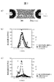
- FIG. 7 is a diagram for explaining the contents analyzed for the emission distribution observed in this example.
- FIG. 7A is a diagram for explaining an analysis target region with respect to an image showing a light emission distribution photographed in the manner of FIG.
- the background light intensity in the figure is 2 with respect to a 0.1 N nitric acid solution containing 100 ppm of lead by using two types of bandpass filters with a center wavelength of 420 nm and a center wavelength of 450 nm as the optical filter 125 of FIG.
- a bandpass filter having a center wavelength of 405 nm and a half-value width of 10 nm is used as the optical filter 125 shown in FIG. 1 by taking two emission images and extrapolating in the wavelength direction in consideration of the wavelength dependence of the transmittance of each bandpass filter. It was obtained from an estimated image of background light.
- the net emission intensity of lead in the figure is based on an image taken using a bandpass filter having a center wavelength of 405 nm and a half-value width of 10 nm as the optical filter 125 of FIG. 1 with respect to a 0.1 N nitric acid solution containing 100 ppm lead. Obtained from an image obtained by subtracting the estimated background light image.
- FIG. 7B is an example of an analysis result for the light emission distribution of the first light emission, that is, the voltage application pulse width of 0.8 milliseconds.
- FIG. 7 (c) subtracts an analysis image of 0.8 milliseconds from an analysis image of a voltage application pulse width of 1.8 milliseconds, which is substantially between 0.8 milliseconds and 1.8 milliseconds, that is, 2 It is an example of the result of having created and analyzed the analysis image with respect to the light emission distribution of the 2nd light emission. It can be seen that the net light emission of lead takes a maximum value near the narrow portion, but the distribution is biased toward the minus side of the x-axis, that is, the plus pole side, and there is a maximum point around minus 2 mm. In addition, the background light tends to be high near the narrow portion and low on the left and right sides, although there is some fluctuation.
- the second light emission shown in FIG. 7C Compared with the first light emission shown in FIG. 7B, the second light emission shown in FIG. 7C has a high light emission intensity as a whole, a low background light intensity, and an S / B of about 10 times larger. Therefore, detection sensitivity and detection accuracy can be significantly increased by performing measurement only for the second light emission.
- the increase in emission intensity is thought to be due to the use of severe experimental conditions in which bubbles and plasma are larger than the narrow part.
- the second light emission is larger than the first light emission under the condition that the bubble is sufficiently large, the element to be analyzed is scattered in the light emission region, and the bubble is sufficiently large. After the current exceeds the peak, the generation amount of Joule heat decreases, the temperature decreases, and the pressure of the gas-liquid interface where the bubbles contract is slow even though the internal pressure of the bubbles decreases, so the pressure is reduced. This is probably because of this.
- the background light is smaller in the second light emission than in the first light emission because of the reduced pressure condition as described above, and one of the reasons is that the frequency of recombination of electrons decreases. it is conceivable that.
- the emission intensity of the net light emission of lead is about 1/3 compared to the maximum value in the narrow portion, but it is a maximum.
- the background light intensity becomes very low, and as a result, the S / B becomes very large.
- the S / B is about 10 times larger when compared with the vicinity of the narrow portion at the time of the second light emission, and S / B is about 200 times larger when compared with the time of the first light emission.
- the vicinity of minus 2 mm corresponds to the vicinity of the gas-liquid interface on the plus pole side, but the detection sensitivity and the detection accuracy can be greatly increased by measuring in this region.
- the net emission of lead is unevenly distributed on the plus pole side as viewed from the narrow portion, and if the area on the plus pole side is the center of the measurement object, the net emission intensity is It can be seen that measurement with a high S / B is possible and detection sensitivity and detection accuracy are greatly increased.
- the height at the narrow portion is high. It can be seen that the background light intensity is avoided and the net emission is sufficiently high, resulting in a high S / B. If the length of the narrow portion is representatively 0.4 mm as the size of the narrow portion, the distance from the center of the narrow portion to the center of the measurement target area is about twice or about three times the size of the narrow portion, Alternatively, the detection sensitivity and detection accuracy can be greatly increased by setting the position to about 5 times.
- the term “much larger” means about 5 times, or about 10 times, or about 20 times, but is not limited thereto.
- the size can be about 2 times to about 100 times or more, which is effective.
- the detection sensitivity and the detection accuracy are greatly increased by setting the region other than the narrow portion in the flow channel as the measurement target region. be able to. Since light emission is caused by plasma generated in the bubble, in order to measure the region other than the narrow portion, it is essential that the bubble and the plasma spread to the region other than the narrow portion. What is possible is as illustrated and described in the present embodiment. In addition, since bubbles and plasma are generated in the flow channel, the measurement target region is limited to the flow channel.
- the center of the measurement target region is narrow.
- the detection sensitivity and the detection accuracy can be greatly increased by being separated from the center of the part by, for example, 0.6 mm, 0.8 mm, 1 mm, or 2 mm.
- the center of the measurement target area is about twice, about three times, or about five times the size of the narrow part from the center of the narrow part.
- the detection sensitivity and the detection accuracy can be greatly increased by setting the region on the positive electrode side as the measurement target region. In this case, it is effective if it is on the positive pole side from the center of the narrow portion of the flow path. In particular, the detection sensitivity and the detection accuracy can be greatly increased by including the region near the gas-liquid interface on the positive electrode side in the measurement target region.
- the detection sensitivity and the detection accuracy are obtained by emitting light a plurality of times by applying a single voltage and measuring only the specific light emission. Measurement with high reproducibility can be realized.
- the light emission intensity is increased, and in particular, it is possible to measure the light emission intensity at the second light emission.
- the ratio between the net light intensity and the background light intensity is high, and measurement with high detection sensitivity is possible.
- the term “multiple times” means at least twice, but the present invention is not limited to this. It is possible to perform from 2 times to 10 times or 100 times, which is effective.
- Example 2 In this embodiment, an example of a plasma emission analyzer that controls the measurement position and the measurement timing will be described.
- FIG. 8 is a diagram showing a configuration example of the plasma emission spectroscopic apparatus of the present embodiment.
- the peripheral portion of the channel 101 is the same as that in FIG.
- the optical fiber end 201 is directed to the flow path 101 and installed on the opposite side of the connectors 105 and 110.
- the optical fiber end 201 is fixed to the stage 202 and can be moved by moving the stage 202.
- the relative position with respect to the flow path 101 can be arbitrarily changed, and light emission from an arbitrary position of the flow path 101 can be changed to the other. The light can be received separately from the light emission from the position.
- the optical fiber end 201 is located closer to the positive pole side than the narrow portion of the flow path, and the positive pole side in the flow path is the measurement target.
- the optical fiber end 201 is an end of the optical fiber 203, and the other end of the optical fiber 203 is connected to the spectrometer 204.
- the light received by the optical fiber end 201 is input to the spectroscope 204 via the optical fiber 203 and dispersed.
- the spectroscope 204 is connected to the computer 122 via the signal line 206, and the spectroscope 204 can be controlled from the computer 122.
- a spectroscope 204 is connected with a CCD camera 205 with an image intensifier (hereinafter referred to as II) as a detector, and receives light dispersed by the spectroscope 204.
- the CCD camera with II 205 is connected to the computer 122 via the signal line 207, and the CCD camera 205 with II can be controlled from the computer 122.
- Information on the spectral spectrum measured by the CCD camera 205 with II is recorded in the storage device of the computer 122 and can be processed.
- the pulse generator 208 is connected to the computer 122 via the signal line 209.
- the power control signal output from the computer 122 to the power supply 116 is also input to the pulse generator 208 in the same manner.
- the pulse generator 208 is connected to the CCD camera 205 with II via a signal line 211.
- the pulse generator 208 receives a power supply control signal, does not process the signal at all, or processes the signal and outputs it as an exposure control signal for the CCD camera 205 with II.
- the II-attached CCD camera 205 operates by receiving an exposure control signal, and can receive the light separated by the spectroscope 204 to obtain a spectral spectrum.
- the pulse generator 208 is connected to the ammeter 115 via the signal line 210.
- the pulse generator 208 receives information on the current measured by the ammeter 115, processes and outputs an exposure control signal for the CCD camera 205 with II under preset conditions, and a CCD camera with II. 205 exposure control can be performed.
- a 0.1 N nitric acid solution containing 100 ppm of lead was supplied as a sample solution to the flow path 101, and voltage was applied to measure light emission.
- the procedure is the same as in the first embodiment, and detailed description thereof is omitted.
- the conditions were a voltage of 2.5 kV, a voltage application pulse width of 1.8 milliseconds, and the number of pulses of 60 times.
- the pulse generator 208 of FIG. 8 inputs a signal for performing exposure for 0.8 milliseconds immediately after voltage application to the CCD camera 205 with II. Also, for the latter second light emission, the pulse generator 208 generates a signal for performing exposure for 1.0 millisecond from 0.8 millisecond after voltage application to 1.8 millisecond. Input to the camera 205.
- FIG. 9 is a diagram for explaining an example of a spectral spectrum of light emission measured in this example.
- An emission line derived from lead (405.78 nm) can be confirmed.
- the net light emission intensity of lead is indicated as S and the background light intensity is indicated as B.
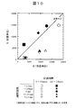
- FIG. 10 is a diagram for explaining the analysis result of the light emission measured in this example.
- spectral spectra for 60 pulses were obtained, the set of S and B exemplified in FIG. 9 was calculated, and the average value was displayed.
- the optical fiber end 201 is moved, and light emission from various positions in the flow channel 101 is examined.
- the distance from the center of the narrow portion to the measurement target region is about three times and about six times when the narrow portion has a length of 0.4 mm as the size of the narrow portion.
- the measurement is performed according to a predetermined measurement timing.
- the apparatus configuration shown in FIG. It is possible to start the measurement and end the measurement when another condition is satisfied, or perform the measurement only when the current value satisfies a certain condition. For example, it is possible to perform control so that measurement starts when the current value exceeds a set threshold value, and then stops measurement when the current value falls below another set threshold value. It is also possible to perform measurement only in a time segment where the current value is equal to or greater than a set threshold value. For example, in the case of FIG. 13 described later, it is effective to perform the above measurement using, for example, 30 milliamperes as a threshold value.
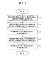
- the measurement procedure for the first example is as shown in the flowchart of FIG. That is, the sample solution is sent to the flow path, a voltage is applied to measure the time change of the current (S11), and a trigger signal for starting measurement is issued when the current value satisfies the preset discrimination condition (S12).
- the measurement is started based on the trigger signal for starting the measurement (S13), and when the current value satisfies the discrimination condition set in advance, the trigger signal for stopping the measurement is issued (S14), and the measurement is stopped based on the trigger signal for stopping the measurement. (S15).
- the measurement procedure can be similarly shown for other cases.
- the exposure time is set by the time of the first light emission and the second light emission, but it is also possible to set a more limited exposure time and set better measurement conditions.
- the measurement timing is controlled by using the information of the time change of the current when the voltage is applied, so that the detection sensitivity and the detection accuracy are high and reproducibility. High measurement can be realized.
- Using the information on the time change of the current at the time of applying the voltage means using the information on the time change of the current value acquired in advance to control to perform measurement in a predetermined time interval.
- While applying voltage to the sample solution monitor the current value at the same time, and use the criteria based on the current value to control the measurement within the same voltage application pulse time. Cases are also included.
- One of the effects peculiar to the present embodiment when compared with the first embodiment is that the measurement start time and the measurement end time can be freely set, and a step of performing a difference in two time intervals is not required. That is. Another unique effect is that measurement control of light emission can be performed directly using the measured current value. Another specific effect is that it is possible to select a specific position in the flow path and perform measurement at a specific time.
- the measurement position can be moved, but a device configuration fixed at a preset position is also possible.
- the measurement position is determined on the measurement device side, not on the flow path, and the measurement position is determined by providing a window at a specific position on the flow path using a material that does not transmit light. It is also possible to determine and measure.
- the measurement timing control is realized by using a CCD camera with II, but an apparatus configuration that controls the measurement timing using a shutter instead is also possible. In that case, an apparatus configuration that sends a control signal to the shutter may be used.
- Example 3 In this embodiment, an example of a plasma emission analyzer that controls the time domain for measurement and analysis using information on the measured current value will be described.
- FIG. 12 is a diagram showing a configuration example of the plasma emission spectroscopic apparatus of the present embodiment.
- the peripheral portion of the channel 101 is the same as that in FIG.
- the optical filter 301 is installed in the vicinity of the flow path 101 and is installed on the opposite side of the connectors 105 and 110.
- An optical slit 302 was installed behind the optical filter 301, and a photomultiplier tube 303 was installed immediately thereafter.
- a high-voltage power supply 304 for the photomultiplier tube is connected to the photomultiplier tube 303 via the electric wire 305 and supplies power to the photomultiplier tube 303.
- the output from the photomultiplier tube 303 is recorded in the memory of the computer 122 via the signal line 306 and analyzed.
- a 0.1 N nitric acid solution containing 100 ppm of lead was supplied as a sample solution to the channel 101, and voltage was applied to measure light emission.
- the procedure is the same as in the first embodiment, and detailed description thereof is omitted.
- the conditions were a voltage of 2.5 kV, a voltage application pulse width of 1.8 milliseconds, and a pulse count of 100 times.
- FIG. 13 is a diagram for explaining an example of the analysis result of the light emission measured in this example.
- FIG. 13A is a graph in which the time change of light emission and the time change of current are recorded simultaneously using a bandpass filter having a center wavelength of 405 nm and a half-value width of 10 nm as the optical filter 301.
- the broken line is the current waveform measured by the ammeter 115
- the solid line is the emission intensity measured by the photomultiplier tube 303.
- the first light emission it can be seen that the light emission peak is slightly delayed in time compared to the current peak.
- the second light emission the light emission intensity suddenly rises as the current suddenly increases, and the current decreases. It can be seen that the emission intensity decreases rapidly.
- FIG. 13 (b) is a graph showing the change over time in the net emission of lead (S) and the background light (B).
- the solid line represents the net light emission (S) of lead, and the broken line represents the background light (B).
- the data for 100 pulses are averaged and normalized by their maximum values. From this result, it can be seen that the behavior of S and B over time is not the same. For example, in the first light emission, S emits light later than B, whereas in the second light emission, S rises earlier than B.
- FIG. 13 (c) is a graph showing the change over time of the ratio (S / B) between the net emission of lead (S) and the background light (B).
- the time change of S / B is calculated based on the time change of S and B calculated by averaging the data for 100 pulses, and normalized by the maximum value.
- the S / B is higher in the second light emission than in the first light emission. That is, if the second light emission is measured, the S / B is high, and as a result, measurement with high detection sensitivity can be realized.
- the S / B is high in the second half. This is because S rises later than B.
- the above measurement can be set to measure from the measurement start time set in advance to the measurement end time after voltage application, or it can be measured over the entire voltage application pulse width, Data can be recorded in a storage device such as a memory of a computer, and a measurement result in a predetermined time interval can be selected and used for analysis.
- the method described here can also be executed by performing a pre-scan.
- the time change of plasma emission is measured as a pre-scan, and the result of the pre-scan is calculated to estimate a time zone in which the emission intensity from the measurement target substance is high.
- the result of the pre-scan is calculated to estimate a time zone in which the emission intensity from the measurement target substance is high.
- it is sufficiently effective to select a region where the ratio of the emission intensity from the measurement target substance to the maximum value is 0.3 or more. After that, if measurement is performed for this time zone, highly sensitive measurement is possible.
- the time change of the plasma emission is measured as a pre-scan
- the calculation is performed on the result of the pre-scan, the net emission intensity from the measurement target substance and the others Estimate the time zone in which the ratio of the background light intensity from the above substances is high.
- the time change of the plasma emission is measured as a pre-scan
- the calculation is performed on the result of the pre-scan, and the variation in the emission intensity from the measurement target substance is small.
- Estimate the band For example, if a region having a variation coefficient of 10% or less is selected, it is sufficiently effective. For example, when the number of voltage applications is set to 100 and the measurement results are integrated, the coefficient of variation is proportional to 1 / 0.5th of the number of integrations. Can be implemented.
- Embodiment 2 One of the unique effects of this embodiment when compared with Embodiment 2 is that it is not always necessary to set the measurement time in advance. It is possible to record the light emission and current time change data for all the time within the voltage application time in the storage device, perform information processing after data acquisition, set the appropriate measurement time division and analyze it is there. Accordingly, a measurement result with high S / B and high detection sensitivity can be obtained with certainty.
- Example 4 when measuring the luminescence by applying an electric field to the sample solution, the time change of the current is measured at the same time, the composition of the reference solution is adjusted so as to match this time change, and the adjusted reference solution
- a plasma emission analyzer that measures luminescence and estimates the amount of a substance to be analyzed in a sample solution using the measured luminescence intensity will be described.
- a 0.1 N nitric acid solution containing 100 ppm of lead was supplied as a sample solution to the channel 101, and voltage was applied to measure luminescence.
- the procedure is the same as in the first embodiment, and detailed description thereof is omitted.
- the conditions were a voltage of 2.5 kV, a voltage application pulse width of 0.8 milliseconds, and the number of pulses of 100 times.
- FIG. 14 is a diagram showing an example of analysis used for adjusting the reference solution, measuring its luminescence, and estimating the net luminescence intensity from the substance to be analyzed in the sample solution.
- FIG. 14A shows the time change of light emission (indicated by T in the figure) measured using a bandpass filter having a center wavelength of 405 nm and a half width of 10 nm as the optical filter 301, and the net emission of lead (S). It is a graph which shows the time change of background light (B). Similar to the method described in the first embodiment, the background light (B) is estimated by extrapolating from a measurement result using a bandpass filter having center wavelengths of 420 nm and 450 nm and a half width of 10 nm. In other words, the background intensity was estimated using information on measurement results at other wavelengths.
- the net emission intensity (S) of lead was estimated from the emission intensity (T) measured with a bandpass filter having a center wavelength of 405 nm and a half-value width of 10 nm, using information on measurement results at other wavelengths (B) Was subtracted.
- FIG. 14B was measured using a reference solution adjusted by changing the ratio of concentrated nitric acid and water so as to match the time change of the current acquired during the measurement of FIG. 14A and this time change.
- the time change of the current is shown.
- the solid line represents the time change of the current with respect to the sample solution, and the broken line represents the time change of the current with respect to the adjusted reference solution.
- Each is an average of 100 pulses. It can be seen that by adjusting the mixing ratio of concentrated nitric acid and water, it is possible to make the time change of the current of the reference solution substantially coincide with the time change of the current for the sample solution.
- FIG. 14C shows the time change (T) of light emission measured using a bandpass filter having a center wavelength of 405 nm and a half-value width of 10 nm as the optical filter 301, as shown in FIG. 14 (b) luminescence time change (R) measured using the same filter and lead luminescence calculated by subtracting the light emission of the aforementioned reference solution from the background light It is a time change (TR) of intensity. That is, the emission intensity of the reference solution is estimated to be equivalent to the background light intensity.
- the emission intensity of the reference solution prepared by the method of FIG. 14B is estimated from the background light. It can be used as. That is, by using the luminescence intensity of the prepared reference solution, it is possible to estimate the net luminescence intensity from the substance to be analyzed in the sample solution. By accurately knowing the net emission intensity, the amount of the substance to be analyzed in the sample solution can be accurately estimated.
- the composition of the sample solution is not known, so in order to match the time change of the current, record the time change of the current for the solution with the mixing ratio changed little by little and refer to the time changes of the current to match each other. It is necessary to determine the composition of the solution. Even if the main solution composition is known, the temporal change in current when a voltage is applied to a solution actually prepared separately to emit light is different from that of the sample solution. Even when the electrical conductivity of the sample solution is measured and the reference solution is adjusted to match the value of the electrical conductivity, a difference appears in the temporal change in current due to subtle mismatch.
- Factors that determine the temporal change in current depend not only on the electrical conductivity of the solution, but also on the state of generation of bubbles and plasma, impurities in the flow path, the state of attached bubbles, and the like. For this reason, it is not possible to make the time changes of the currents coincide with each other only by matching the electric conductivities, and the light emission intensity cannot be considered equivalent to the background light. On the other hand, if a reference solution in which the time change of current during voltage application is adjusted with the sample solution is used, the emission intensity may be considered to be equivalent to the background light of the sample solution as in the above example.
- the reference solution can usually be prepared with a combination of acids, such as nitric acid and water, which are expected to constitute the main part of the sample solution. It is also appropriate to combine other acids, hydrochloric acid, sulfuric acid, etc. that are often used in elemental analysis. Since it is important that there is electrical conduction, it is possible to combine solutions containing salts such as sodium chloride. In addition, when the sample solution contains an organic solvent, it is also appropriate to combine the organic solvents.
- FIG. 15 is a diagram showing a configuration example of another plasma emission analyzer of the present embodiment.
- the parts related to measurement such as the peripheral part of the flow channel 101 and the peripheral part of the electron multiplier 303, are the same as those in FIG.
- description related to the syringe pump 109 is omitted, an equivalent liquid feeding device is provided.
- the sample solution container 401 for setting the sample solution is connected to the pipe 108 via the switching valve 404.
- a container 402 and a container 403 containing a solution for adjusting a reference solution are connected to the pipe 108 via a mixer 405.
- the switching valve 404 and the mixer 405 are connected to the computer 122 via signal lines 406 and 407, respectively.
- the switching valve 404 is switched by a signal from the computer 122, so that a sample solution or a reference solution including a preparation process can be sent to the channel 101.
- the mixer 405 can be operated by a signal from the computer 122 to mix the solutions in the container 402 and the container 403 at an arbitrary ratio and send them.
- the combination of solutions for adjusting the reference solution is the same as that already described.
- FIG. 16 is a flowchart showing the measurement procedure in this example.
- a sample solution is sent to a flow path, a voltage is applied, light emission is measured, and simultaneously a time change of current is measured (S21).
- the time change of the current is measured by changing the mixing ratio of the acid and water, and the reference solution is prepared by mixing the acid and water at a mixing ratio where the time change of the current is the same as that of the sample solution (S22).
- the reference solution adjusted as described above is sent to the channel, voltage is applied, light emission is measured, and this light emission is estimated as background light (S23).
- the estimated background light is subtracted from the luminescence of the sample solution to estimate the net luminescence intensity, and the amount of the analyte in the sample solution is estimated using the estimated net luminescence intensity (S24).
- the reference solution it is desirable to use the same type of acid when the type of acid in the sample solution is known.
- Nitric acid is often used for elemental analysis, so it is often appropriate to use nitric acid. Since acid is often used for elemental analysis, it is assumed that a reference solution is prepared by mixing acid and water. However, when the electrical conductivity of the sample solution is mainly derived from a dissolved salt It is also appropriate to prepare a reference solution by mixing a solution of the corresponding salt with a high concentration and water.
- a solution containing no analysis target substance and a solution containing the analysis target substance together as a reference solution.
- To estimate the amount of analyte in the sample solution usually prepare and measure several solutions containing the analyte of known concentration, and create and use a calibration curve that uses this luminescence.
- a reference solution a solution containing a substance to be analyzed whose current changes with time are matched, and a calibration curve indicating a net light emission amount with respect to the concentration is prepared and used.
- the time change of the current is measured at the same time, the composition of the reference solution is adjusted to match this time change, and the adjusted reference is made.
- light emission is measured with a photomultiplier tube through an optical filter, and the time change of light emission is also measured, but the measurement of light emission is not limited to this means, and the time change of light emission is also measured. It is not always necessary.
- a spectroscope may be used, and it is also appropriate to use photodetectors such as CCD cameras, photodiodes and photodiode arrays.
- the current measurement it is important to measure the time change, compare the time changes of the currents, and match the time changes of the currents by adjusting the solution.
- the net emission intensity can be accurately estimated, so that the detection sensitivity and detection accuracy can be improved.
- the structure may be sufficient, and the apparatus can be miniaturized. As a result, an inexpensive analyzer can be realized.
- FIG. 17 is a diagram for explaining an example of the flow path used in the present embodiment.
- the channel has a narrow portion with a length of 400 ⁇ m and a depth of 33 ⁇ m.
- the electrodes were installed at the left and right ends of the flow path, and the left side of the figure was the negative pole and the right side of the figure was the positive pole.
- the channel shown in FIG. 17 was filled with 0.1 ppm nitric acid solution of 50 ppm potassium as a sample solution, and a voltage of 1260 V was applied for 30 milliseconds.
- voltage was applied without performing liquid feeding. Observation was performed using a high-speed camera.
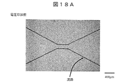
- FIG. 18A is an example of an image obtained by photographing the state of the flow path before voltage application.
- the region surrounded by the flow path wall indicated by the arrow in the figure is filled with the sample solution, and at this time, there is no gas-liquid interface and no light emission.
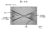
- FIG. 18B is an example of an image obtained by photographing the flow path after 100 microseconds after voltage application.
- gas-liquid interfaces can be seen on both the left and right sides as seen from the center of the narrow portion.
- the left side is the gas-liquid interface on the negative pole side
- the right side is the gas-liquid interface on the positive pole side.
- the portion sandwiched at the gas-liquid interface of the channel including the narrow portion is a bubble, and the portion outside the gas-liquid interface as viewed from the narrow portion is the sample solution.
- Light emission extending linearly in the left-right direction can be observed at the center of the image in FIG. 18B. This is light emission from the potassium solution. It can be seen that this light emission is strong on the negative pole side on the left side from the center of the narrow portion and reaches the gas-liquid interface on the negative pole side.
- FIG. 19 shows the distribution of the emission intensity from the potassium solution with respect to the x-axis, which is the horizontal direction in FIG.
- the region x corresponding to the narrow portion is clearly shown.
- the emission intensity from the potassium solution is higher on the minus pole side than the narrow portion.
- the light emission intensity is highest at a position of about 400 ⁇ m as measured from the center of the narrow portion, and is about 1 times as long as the length of the narrow portion is 400 ⁇ m.
- this invention is not limited to the above-mentioned Example, Various modifications are included.
- the above-described embodiments have been described in detail for easy understanding of the present invention, and are not necessarily limited to those having all the configurations described.
- a part of the configuration of one embodiment can be replaced with the configuration of another embodiment, and the configuration of another embodiment can be added to the configuration of one embodiment.
- the functions, processing units, processing means, and the like of the above configuration may be realized by hardware by designing a part or all of them with, for example, an integrated circuit.
- Each of the above-described configurations, functions, and the like may be realized by software by interpreting and executing a program that realizes each function by the processor.
- Information such as programs, tables, and files for realizing each function can be stored in a recording device such as a memory, a hard disk, or SSD (Solid State Drive), or a recording medium such as an IC card, SD card, or DVD.
- signal lines and electric wires are those that are considered necessary for explanation, and not all control lines and information lines on the product are necessarily shown. Actually, it may be considered that almost all the components are connected to each other.
- this invention is the element, solution composition, flow path shape, and measurement as described in the Example. It is not limited to the conditions.
Landscapes
- Health & Medical Sciences (AREA)
- Nuclear Medicine, Radiotherapy & Molecular Imaging (AREA)
- Physics & Mathematics (AREA)
- Life Sciences & Earth Sciences (AREA)
- Chemical & Material Sciences (AREA)
- Analytical Chemistry (AREA)
- Biochemistry (AREA)
- General Health & Medical Sciences (AREA)
- General Physics & Mathematics (AREA)
- Immunology (AREA)
- Pathology (AREA)
- Investigating, Analyzing Materials By Fluorescence Or Luminescence (AREA)
- Optical Measuring Cells (AREA)
Priority Applications (1)
| Application Number | Priority Date | Filing Date | Title |
|---|---|---|---|
| US14/000,610 US9222890B2 (en) | 2011-03-07 | 2012-01-13 | Plasma spectrometer |
Applications Claiming Priority (2)
| Application Number | Priority Date | Filing Date | Title |
|---|---|---|---|
| JP2011049041A JP5705591B2 (ja) | 2011-03-07 | 2011-03-07 | プラズマ分光分析装置 |
| JP2011-049041 | 2011-03-07 |
Publications (1)
| Publication Number | Publication Date |
|---|---|
| WO2012120919A1 true WO2012120919A1 (ja) | 2012-09-13 |
Family
ID=46797890
Family Applications (1)
| Application Number | Title | Priority Date | Filing Date |
|---|---|---|---|
| PCT/JP2012/050552 Ceased WO2012120919A1 (ja) | 2011-03-07 | 2012-01-13 | プラズマ分光分析装置 |
Country Status (3)
| Country | Link |
|---|---|
| US (1) | US9222890B2 (enExample) |
| JP (1) | JP5705591B2 (enExample) |
| WO (1) | WO2012120919A1 (enExample) |
Cited By (2)
| Publication number | Priority date | Publication date | Assignee | Title |
|---|---|---|---|---|
| EP3306314A1 (en) | 2016-10-07 | 2018-04-11 | ARKRAY, Inc. | Plasma spectroscopic analysis method and inhibitor of plasma emission derived from non-target |
| CN107917906A (zh) * | 2016-10-07 | 2018-04-17 | 爱科来株式会社 | 等离子体分光分析方法和来自非靶材的等离子体发光的抑制剂 |
Families Citing this family (16)
| Publication number | Priority date | Publication date | Assignee | Title |
|---|---|---|---|---|
| CN104865239B (zh) | 2014-02-21 | 2019-03-22 | 爱科来株式会社 | 等离子光谱分析方法 |
| JP6498959B2 (ja) | 2014-02-21 | 2019-04-10 | アークレイ株式会社 | プラズマ分光分析方法 |
| JP6480210B2 (ja) | 2014-02-28 | 2019-03-06 | アークレイ株式会社 | プラズマ発生用チップ、プラズマ発生装置およびプラズマ分光分析方法 |
| JP6480211B2 (ja) | 2014-02-28 | 2019-03-06 | アークレイ株式会社 | プラズマ発生用チップ、プラズマ発生装置およびプラズマ分光分析方法 |
| US9733158B1 (en) * | 2014-08-19 | 2017-08-15 | Elemental Scientific, Inc. | Dilution into a transfer line between valves for mass spectrometry |
| JP6656931B2 (ja) | 2015-01-13 | 2020-03-04 | アークレイ株式会社 | プラズマ分光分析方法およびプラズマ分光分析装置 |
| CN105784675B (zh) * | 2015-01-13 | 2020-01-07 | 爱科来株式会社 | 等离子体分光分析方法和等离子体分光分析装置 |
| CN105004709B (zh) * | 2015-04-13 | 2018-06-15 | 中国地质大学(武汉) | 一种液体放电微等离子体激发源装置及等离子体激发方法 |
| JP2017130334A (ja) * | 2016-01-20 | 2017-07-27 | 株式会社日立ハイテクノロジーズ | 荷電粒子ビーム装置及び荷電粒子ビーム装置の画像形成方法 |
| EP3273228A1 (en) | 2016-07-22 | 2018-01-24 | ARKRAY, Inc. | Plasma spectroscopic analysis method and plasma spectroscopic analyzer |
| JP7009735B2 (ja) * | 2016-09-08 | 2022-01-26 | 株式会社リコー | 画像表示装置及び物体装置 |
| JP6871088B2 (ja) * | 2017-07-05 | 2021-05-12 | アークレイ株式会社 | 炭素電極の洗浄方法 |
| JP7295525B2 (ja) * | 2019-04-24 | 2023-06-21 | 国立大学法人東北大学 | 気泡内圧力測定装置、気泡内圧力測定方法、及び、プログラム、並びに、気泡内圧力評価装置、及び、気泡内圧力評価方法 |
| JP7496767B2 (ja) | 2020-12-15 | 2024-06-07 | 株式会社日立ハイテク | 荷電粒子線装置 |
| US11598727B1 (en) * | 2021-08-19 | 2023-03-07 | 2S Water Incorporated | Solution glow discharge plasma chamber with lens |
| US20240295475A9 (en) * | 2022-08-02 | 2024-09-05 | Aditi Bhaskar | Portable compound trace detection device |
Citations (4)
| Publication number | Priority date | Publication date | Assignee | Title |
|---|---|---|---|---|
| JPH0452551A (ja) * | 1990-06-20 | 1992-02-20 | Hitachi Ltd | 成分分析方法及び装置 |
| JP3932368B2 (ja) * | 2004-03-25 | 2007-06-20 | 国立大学法人北陸先端科学技術大学院大学 | プラズマ発生装置 |
| JP2010197358A (ja) * | 2009-02-27 | 2010-09-09 | Tokai Kogaku Kk | 分光分析装置及び元素分析装置 |
| JP2011180045A (ja) * | 2010-03-02 | 2011-09-15 | Japan Advanced Institute Of Science & Technology Hokuriku | プラズマ発生手段、プラズマ発生装置及び元素分析方法 |
Family Cites Families (1)
| Publication number | Priority date | Publication date | Assignee | Title |
|---|---|---|---|---|
| GB9825722D0 (en) * | 1998-11-24 | 1999-01-20 | Imperial College | Plasma chip |
-
2011
- 2011-03-07 JP JP2011049041A patent/JP5705591B2/ja not_active Expired - Fee Related
-
2012
- 2012-01-13 US US14/000,610 patent/US9222890B2/en not_active Expired - Fee Related
- 2012-01-13 WO PCT/JP2012/050552 patent/WO2012120919A1/ja not_active Ceased
Patent Citations (4)
| Publication number | Priority date | Publication date | Assignee | Title |
|---|---|---|---|---|
| JPH0452551A (ja) * | 1990-06-20 | 1992-02-20 | Hitachi Ltd | 成分分析方法及び装置 |
| JP3932368B2 (ja) * | 2004-03-25 | 2007-06-20 | 国立大学法人北陸先端科学技術大学院大学 | プラズマ発生装置 |
| JP2010197358A (ja) * | 2009-02-27 | 2010-09-09 | Tokai Kogaku Kk | 分光分析装置及び元素分析装置 |
| JP2011180045A (ja) * | 2010-03-02 | 2011-09-15 | Japan Advanced Institute Of Science & Technology Hokuriku | プラズマ発生手段、プラズマ発生装置及び元素分析方法 |
Non-Patent Citations (1)
| Title |
|---|
| ISAO KUMAGAYA ET AL.: "Micro Ryutaichu no Plasma o Mochiita Genso Bunseki no Anteika", CHEMICAL SENSORS, vol. 23, no. A, 29 March 2007 (2007-03-29), pages 13 - 15 * |
Cited By (4)
| Publication number | Priority date | Publication date | Assignee | Title |
|---|---|---|---|---|
| EP3306314A1 (en) | 2016-10-07 | 2018-04-11 | ARKRAY, Inc. | Plasma spectroscopic analysis method and inhibitor of plasma emission derived from non-target |
| CN107917906A (zh) * | 2016-10-07 | 2018-04-17 | 爱科来株式会社 | 等离子体分光分析方法和来自非靶材的等离子体发光的抑制剂 |
| US10295471B2 (en) | 2016-10-07 | 2019-05-21 | Arkray, Inc. | Plasma spectroscopic analysis method and inhibitor of plasma emission derived from non-target |
| CN107917906B (zh) * | 2016-10-07 | 2022-05-10 | 爱科来株式会社 | 等离子体分光分析方法和来自非靶材的等离子体发光的抑制剂 |
Also Published As
| Publication number | Publication date |
|---|---|
| US20130321803A1 (en) | 2013-12-05 |
| JP5705591B2 (ja) | 2015-04-22 |
| JP2012185064A (ja) | 2012-09-27 |
| US9222890B2 (en) | 2015-12-29 |
Similar Documents
| Publication | Publication Date | Title |
|---|---|---|
| JP5705591B2 (ja) | プラズマ分光分析装置 | |
| CN102985807B (zh) | 流式粒子分析装置以及流式粒子分析方法 | |
| CN102998240B (zh) | 微粒测量装置 | |
| CN110121643A (zh) | 用于流式细胞仪的光学检测系统、流式细胞仪系统及其使用方法 | |
| CN104949964B (zh) | Icp发光分光分析装置 | |
| JP3260469B2 (ja) | 粒子分析装置 | |
| JP6656210B2 (ja) | 分光蛍光光度計 | |
| WO2015023545A1 (en) | Systems and methods for monitoring phenanthrene equivalent concentration | |
| CN107064111B (zh) | 高重频激光剥离-火花诱导击穿光谱元素分析系统及方法 | |
| JP6413759B2 (ja) | 光学分析装置 | |
| EP2362207A1 (de) | Messsystem und Messverfahren insbesondere zur Blutzuckerbestimmung | |
| CN113133172B (zh) | 一种先导放电起始阶段通道气体瞬态温度测量系统和方法 | |
| JP5798953B2 (ja) | プラズマ分光分析装置 | |
| EP1929280B1 (de) | Laborvorrichtung zur gleichzeitigen durchführung von reaktionen in einer mehrzahl von proben | |
| KR101727009B1 (ko) | 흡광신호 및 형광신호를 이용한 미세입자 측정장치 및 데이터 보정방법 | |
| CN116380888A (zh) | 浊度计以及浊度测量方法 | |
| CN102889928A (zh) | 百兆级带宽光电探测仪器标定方法 | |
| JP2023138053A (ja) | 濃度測定装置 | |
| CN103235186A (zh) | 利用光谱测量电弧阻抗的方法和系统 | |
| AT502194A4 (de) | Verfahren und vorrichtung zur bestimmung der fluoreszenz einer probe sowie verwendung derselben | |
| RU2319937C2 (ru) | СПОСОБ И УСТРОЙСТВО ДЛЯ ОБНАРУЖЕНИЯ СПЕКТРАЛЬНОЙ ЛИНИИ УГЛЕРОДА У 193 нм МЕТОДОМ ОПТИЧЕСКОЙ ЭМИССИОННОЙ СПЕКТРОСКОПИИ | |
| CN114527112B (zh) | 用于光谱仪的诊断测试方法 | |
| KR20050001053A (ko) | 발광소자의 발광 특성 검사 장치 | |
| DE102018220154A1 (de) | Verfahren zum Betreiben eines Partikelsensors | |
| CN121164242A (en) | Transformer oil monitoring device and method without degassing |
Legal Events
| Date | Code | Title | Description |
|---|---|---|---|
| 121 | Ep: the epo has been informed by wipo that ep was designated in this application |
Ref document number: 12755429 Country of ref document: EP Kind code of ref document: A1 |
|
| WWE | Wipo information: entry into national phase |
Ref document number: 14000610 Country of ref document: US |
|
| NENP | Non-entry into the national phase |
Ref country code: DE |
|
| 122 | Ep: pct application non-entry in european phase |
Ref document number: 12755429 Country of ref document: EP Kind code of ref document: A1 |