WO2012120871A1 - 半導体基板、半導体装置および半導体基板の製造方法 - Google Patents
半導体基板、半導体装置および半導体基板の製造方法 Download PDFInfo
- Publication number
- WO2012120871A1 WO2012120871A1 PCT/JP2012/001506 JP2012001506W WO2012120871A1 WO 2012120871 A1 WO2012120871 A1 WO 2012120871A1 JP 2012001506 W JP2012001506 W JP 2012001506W WO 2012120871 A1 WO2012120871 A1 WO 2012120871A1
- Authority
- WO
- WIPO (PCT)
- Prior art keywords
- crystal layer
- pair
- layer
- opening
- crystal
- Prior art date
- Legal status (The legal status is an assumption and is not a legal conclusion. Google has not performed a legal analysis and makes no representation as to the accuracy of the status listed.)
- Ceased
Links
Images


Classifications
-
- G—PHYSICS
- G01—MEASURING; TESTING
- G01R—MEASURING ELECTRIC VARIABLES; MEASURING MAGNETIC VARIABLES
- G01R33/00—Arrangements or instruments for measuring magnetic variables
- G01R33/02—Measuring direction or magnitude of magnetic fields or magnetic flux
- G01R33/06—Measuring direction or magnitude of magnetic fields or magnetic flux using galvano-magnetic devices
- G01R33/07—Hall effect devices
- G01R33/072—Constructional adaptation of the sensor to specific applications
-
- H—ELECTRICITY
- H10—SEMICONDUCTOR DEVICES; ELECTRIC SOLID-STATE DEVICES NOT OTHERWISE PROVIDED FOR
- H10N—ELECTRIC SOLID-STATE DEVICES NOT OTHERWISE PROVIDED FOR
- H10N52/00—Hall-effect devices
- H10N52/101—Semiconductor Hall-effect devices
-
- H—ELECTRICITY
- H10—SEMICONDUCTOR DEVICES; ELECTRIC SOLID-STATE DEVICES NOT OTHERWISE PROVIDED FOR
- H10P—GENERIC PROCESSES OR APPARATUS FOR THE MANUFACTURE OR TREATMENT OF DEVICES COVERED BY CLASS H10
- H10P14/00—Formation of materials, e.g. in the shape of layers or pillars
- H10P14/20—Formation of materials, e.g. in the shape of layers or pillars of semiconductor materials
- H10P14/27—Formation of materials, e.g. in the shape of layers or pillars of semiconductor materials using selective deposition, e.g. simultaneous growth of monocrystalline and non-monocrystalline semiconductor materials
Definitions
- the present invention relates to a semiconductor substrate, a semiconductor device, and a method for manufacturing a semiconductor substrate.
- Patent Document 1 describes a hybrid magnetic sensor in one package. InSb, InAs, GaSb, GaAs, GaAsSb, InAsSb, InGaAs, InGaSb, InGaAsSb, InP, InGaP, InAsP, InGaAsP, InN, GaN, and InGaN are described as materials constituting the sensor portion of the magnetic sensor. Patent Document 1 Japanese Patent Application Laid-Open No. 2004-158668
- An object of the present invention is to provide a semiconductor substrate suitable for manufacturing a p-type carrier Hall element having sufficient sensitivity.
- a base substrate in which all or part of the surface is a silicon crystal surface, and an opening that is located on the base substrate and reaches the silicon crystal surface. And an inhibitor that inhibits crystal growth, a first crystal layer located on the silicon crystal surface exposed by the opening, and a pair of first metals located on the first crystal layer and disposed apart from each other And a pair of second metal layers positioned on the first crystal layer and spaced apart from each other, a first shortest line connecting each of the pair of first metal layers, and a pair of second metal layers Provided is a semiconductor substrate in which the second shortest line connecting each of the metal layers intersects or twists.
- the shape of the first crystal layer viewed from the upper surface side may be a quadrilateral.
- the direction of the first shortest line is equal to the direction of the first diagonal line of the first crystal layer viewed from the upper surface side.
- the direction of the two shortest lines is preferably equal to the direction of the second diagonal line different from the first diagonal line in the first crystal layer as viewed from the upper surface side.
- the first crystal layer is a p-type semiconductor.
- the first crystal layer is preferably Si x Ge 1-x (0 ⁇ x ⁇ 1).
- a second crystal layer made of a III-V compound semiconductor may be further provided between the first crystal layer and the first metal layer or the second metal layer.
- the silicon crystal plane at the bottom of the opening means the silicon crystal plane exposed by the opening.
- the semiconductor substrate includes the first crystal layer as a carrier transport layer, the pair of first metal layers as a pair of main current electrodes, and the pair of second metal layers as a pair.
- a semiconductor device having a Hall element as a pair of detection electrodes is provided.
- the inhibitor may have another opening at a position different from the opening where the Hall element is located.
- the semiconductor device is located at the first crystal layer located at the other opening and the other opening.
- An active element having the first crystal layer as an active layer may be further included, and the Hall element and the active element may be connected to each other by wiring located on the inhibitor.
- the inhibitor may have another opening at a position different from the opening where the Hall element is located.
- the semiconductor device includes the first crystal layer located in the other opening and the other opening. There may be further provided another crystal layer formed on the first crystal layer positioned, and an active element having the other crystal layer as an active layer, and the Hall element and the active element are provided on the inhibitor. They may be connected to each other by wiring located at the positions.
- a step of forming an inhibitor on a base substrate whose whole or part of the surface is a silicon crystal plane a step of forming an opening reaching the silicon crystal plane in the inhibitor, A step of forming a first crystal layer on the silicon crystal surface exposed by the opening by an epitaxial growth method, a step of forming a metal layer on the upper surface of the inhibitor and the first crystal layer, and patterning the metal layer, Forming a main current electrode and a pair of detection electrodes.
- a pair of main current electrodes and a pair of detection electrodes may be formed in an intersecting relationship or a twisted positional relationship.
- the plane of the semiconductor substrate 100 is shown.
- a cross section of a semiconductor substrate 100 is shown.
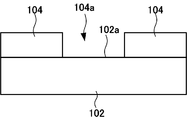
- a cross section in the manufacturing process of the semiconductor substrate 100 is shown.
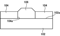
- a cross section in the manufacturing process of the semiconductor substrate 100 is shown.
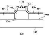
- the cross section of the semiconductor substrate 200 is shown.
- a cross section of a semiconductor substrate 300 is shown.
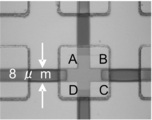
- the microscope picture of the semiconductor substrate of an Example is shown.
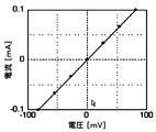
- the current-voltage characteristic of the Hall element of an Example is shown.
- FIG. 1A shows a plane of the semiconductor substrate 100.
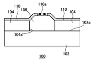
- FIG. 1B shows a cross section of the semiconductor substrate 100. The cross section shown in FIG. 1B is a cross section taken along the line AA in the plane shown in FIG. 1A.
- the semiconductor substrate 100 includes a base substrate 102, an inhibitor 104, a first crystal layer 106, a pair of first metal layers 110, and a second metal layer 112.
- the base substrate 102 has a silicon crystal surface 102a entirely or partially.
- the substrate whose surface is entirely or partially made of silicon crystal include a silicon substrate and an SOI (Silicon-on-Insulator) substrate.
- a silicon substrate is preferable as the base substrate 102.
- a substrate whose surface is entirely or partially silicon crystal it is not necessary to use an expensive compound semiconductor crystal substrate.
- an existing manufacturing apparatus and an existing manufacturing process used in a silicon wafer process can be used, and a substrate having a larger diameter than that of a compound semiconductor substrate can be used. Therefore, the manufacturing cost of the semiconductor substrate 100 can be reduced.
- the inhibitor 104 is located on the base substrate 102 and has an opening 104a that reaches the silicon crystal surface 102a. Inhibitor 104 inhibits crystal growth. Examples of the inhibitor 104 include silicon oxide, silicon nitride, silicon oxynitride, and aluminum oxide.
- the size of the opening 104a is desirably 1 ⁇ m to 100 ⁇ m, more desirably 5 to 50 ⁇ m, and particularly preferably 30 ⁇ m.
- the “size of the opening 104a” is the length of one side when the region of the base substrate 102 exposed by the opening 104a is a square, and the length of the short side when the region is a rectangle. In the case of a shape, it is the length of the minor axis, and in the case of a circle, it is the diameter.
- the first crystal layer 106 is located on the silicon crystal surface 102a exposed through the opening 104a.
- the first crystal layer 106 is preferably made of SiGeCSn, and is preferably made of Si x Ge 1-x (0 ⁇ x ⁇ 1). Examples of the first crystal layer 106 include SiGe, SiC, SiCGe, and the like.
- the first crystal layer 106 is more preferably made of Ge. Since the first crystal layer 106 is formed inside the small opening 104a of 30 ⁇ m or less, the first crystal layer 106 has few crystal defects and is often formed without defects. As a result, the quality of the first crystal layer 106 is improved, and when the second crystal layer is formed on the first crystal layer 106, defects in the second crystal layer are reduced or eliminated, Quality can be improved.
- the first crystal layer 106 may be grown directly on the silicon crystal surface 102a, or may be grown via a Si buffer layer or a SiGe buffer layer.
- the first crystal layer 106 protrudes from the surface of the inhibitor 104 opposite to the surface in contact with the base substrate 102. That is, the thickness of the first crystal layer 106 is larger than the thickness of the inhibitor 104.
- the first crystal layer 106 has a metal contact surface in contact with the pair of first metal layers 110 or the pair of second metal layers 112 between a surface in contact with the inhibitor 104 and a surface opposite to the surface in contact with the base substrate 102.
- the metal contact surface may have an inclination with respect to the stacking direction of the first crystal layer 106.
- the metal contact surface may have a surface parallel to a surface where the first crystal layer 106 is in contact with the inhibitor 104 and a surface parallel to a surface where the first crystal layer 106 is in contact with the base substrate 102.
- the first crystal layer 106 may be recessed with respect to the surface of the inhibitor 104 opposite to the surface in contact with the base substrate 102. That is, the thickness of the first crystal layer 106 may be smaller than the thickness of the inhibitor 104. Also in this case, the first crystal layer 106 includes the pair of first metal layers 110 or the pair of second metal layers 112 between the surface in contact with the inhibitor 104 and the surface opposite to the surface in contact with the base substrate 102. It has a metal contact surface in contact.
- the first crystal layer 106 can be a p-type semiconductor. By using a p-type semiconductor, a p-type carrier Hall element can be formed.
- the pair of first metal layers 110 are positioned on the first crystal layer 106, and the first metal layers 110 are arranged apart from each other.
- the pair of second metal layers 112 are located on the first crystal layer 106, and the respective second metal layers 112 are disposed apart from each other.
- the first shortest line 110a that connects each of the pair of first metal layers 110 and the second shortest line 112a that connects each of the pair of second metal layers 112 are in an intersecting relationship or a twisted positional relationship.
- the first shortest line 110a and the second shortest line 112a may be in the same plane, and the first shortest line 110a and the second shortest line 112a are in different planes and are not parallel to each other. , May be in a twisted relationship.
- the semiconductor substrate 100 can be It functions as a Hall element of the mold.
- the metal layer is, for example, a single layer of Au, AuGe, or Ni or a laminate of two or more thereof.
- the first shortest line 110a and the second shortest line 112a preferably intersect at an angle of approximately 90 ° when viewed from above the plane on which the first metal layer 110 or the second metal layer 112 is formed.
- the shape of the first crystal layer 106 viewed from the upper surface side is, for example, a quadrilateral.
- the shape of the first crystal layer 106 viewed from the upper surface side may be a square.
- the direction of the first shortest line 110a that connects each of the pair of first metal layers 110 is, for example, the same as the direction of the first diagonal line that is one of the two diagonal lines of the first crystal layer 106 viewed from the upper surface side.
- the direction of the second shortest line 112a connecting each of the pair of second metal layers 112 is equal to the direction of the second diagonal line different from the first diagonal line among the two diagonal lines of the first crystal layer 106 viewed from the upper surface side.
- the shape of the first metal layer 110 and the second metal layer 112 viewed from the upper surface side is a quadrilateral.
- the shapes of the first metal layer 110 and the second metal layer 112 viewed from the upper surface side may be square.
- a region where each of the first metal layer 110 and the second metal layer 112 overlaps the first crystal layer 106 is a quadrilateral when viewed from the upper surface side.
- the first crystal layer 106, the first metal layer 110, and the second metal layer 112 have a square shape when viewed from the upper surface side, and when viewed from the upper surface side, the first metal layer 110 and the second metal layer 112 each have the first shape.
- a region overlapping with one crystal layer 106 may be a square.
- the region where each of the first metal layer 110 and the second metal layer 112 overlaps the first crystal layer 106 is formed in a quadrilateral region at the four corners of the first crystal layer 106.
- the pair of first metal layers 110 and the pair of second metal layers 112 are formed in the quadrangular regions at the four corners of the first crystal layer 106 and the inhibitor 104, so that the first crystal layer 106 is minute. Even in this case, the first metal layer 110 and the second metal layer 112 can be easily formed.
- the first crystal layer 106 is a carrier transport layer
- the pair of first metal layers 110 is a pair of main current electrodes
- the pair of second metal layers 112 is a pair of detection electrodes.
- other semiconductor substrates described below can also function as Hall elements.
- the pair of first metal layers 110 and the pair of second metal layers 112 include the first shortest line 110 a that connects the pair of first metal layers 110 and the pair of second metal layers 112. Since the second shortest line 112a that connects the two intersects each other or has a twisted positional relationship, a Hall element in the semiconductor device can be configured. And since the said Hall element has a p-type carrier, a p-type Hall element can be comprised. Furthermore, since the crystal quality of the first crystal layer 106 is good, high sensitivity can be realized even with a p-type carrier Hall element.
- FIGS. 2 and 3 show cross sections of the semiconductor substrate 100 in the manufacturing process.
- the inhibitor 104 is formed on the base substrate 102, and the opening 104 a reaching the silicon crystal surface 102 a is formed in the inhibitor 104.
- a first crystal layer 106 made of Si x Ge 1-x (0 ⁇ x ⁇ 1) is formed on the silicon crystal surface 102a exposed through the opening 104a by an epitaxial growth method.
- a CVD (Chemical Vapor Deposition) method or a MOCVD (Metal Organic Chemical Vapor Deposition) method can be used.
- GeH 4 (germane) can be used as the Ge source
- SiH 4 (silane) or Si 2 H 6 (disilane) can be used as the Si source.
- MOCVD tBuGe (tertiary butyl germane) is used for the Ge source
- TMeSi tetramethylsilane
- SiSource trimethylindium
- TMGa trimethylgallium
- TMAl trimethylaluminum
- AsH 3 arsine
- PH 3 phosphine
- NH 3 ammonia
- TMSb Trimethylantimony
- Hydrogen can be used as the carrier gas.
- the reaction temperature is preferably in the range of 300 ° C to 1100 ° C, more preferably in the range of 450 to 750 ° C.
- the preferred reaction temperature varies depending on the composition of crystals formed by the epitaxial growth method.
- the thickness of the epitaxial growth layer can be controlled by appropriately selecting the reaction time.
- a metal layer is formed on the top surfaces of the inhibitor 104 and the first crystal layer 106, and the metal layer is patterned to form a pair of first metal layers 110 and a pair of second layers.
- a metal layer 112 is formed. In this way, the semiconductor substrate 100 shown in FIGS. 1A and 1B can be manufactured.
- the first crystal layer 106 is preferably annealed.
- the first crystal layer 106 with good crystal quality is obtained by annealing.
- an insulator may be embedded in the trace of etching (patterning) the metal layer. Examples of the insulator in this case include silicon oxide, silicon nitride, silicon oxynitride, and aluminum oxide.
- FIG. 4 shows a cross section of the semiconductor substrate 200.
- the semiconductor substrate 200 includes a second crystal layer 202 in addition to the members of the semiconductor substrate 100.
- the second crystal layer 202 is located between the first crystal layer 106 and the first metal layer 110 or the second metal layer 112.
- the second crystal layer 202 is made of a III-V group compound semiconductor.
- the second crystal layer 202 may be made of InGaAlAsPNSb, and preferably made of InGaAlAsP. Examples of the second crystal layer 202 include GaAs, InSb, InAs, GaP, InP, GaN, InN, and AlN. Since the second crystal layer 202 is formed on the first crystal layer 106 having good crystallinity, the second crystal layer 202 has few crystal defects and is often formed without defects.
- the second crystal layer 202 is preferably lattice-matched or pseudo-lattice-matched with the first crystal layer 106.
- the second crystal layer 202 with good crystallinity can be obtained by lattice matching or pseudo-lattice matching with the first crystal layer 106 with good crystallinity.
- the first crystal layer 106 is Ge
- the second crystal layer 202 is preferably GaAs, InGaAs, InGaAsP, or InGaAsN that is lattice-matched or pseudo-lattice-matched with the first crystal layer 106.
- the second crystal layer 202 can be a crystal lattice-matched or pseudo-lattice-matched with GaAs.
- the second crystal layer 202 formed on the high quality Ge crystal is preferable because it becomes a higher quality crystal.
- the second crystal layer 202 may be two crystal layers having different compositions. By making the band gaps of the two crystal layers different from each other, a hetero barrier can be formed at the interface between the two crystal layers. The layer for generating carriers and the layer for moving carriers can be separated from each other with the hetero barrier as a boundary. Therefore, higher carrier mobility can be obtained. As a result, a Hall element with further improved sensitivity can be obtained.
- the second crystal layer 202 may be composed of three or more crystal layers.
- a quantum well can be formed by these three or more crystal layers, and higher mobility can also be obtained by reducing the impurity atom concentration of the quantum well layer. Thereby, a Hall element with further improved sensitivity can be obtained.
- a Hall element having a sufficiently high mobility of the p-type carrier can be obtained. Therefore, a complementary circuit can be configured by combining a Hall element of a p-type carrier and a Hall element of an n-type carrier.
- FIG. 5 shows a cross section of the semiconductor substrate 300.
- the inhibitor 104 has another opening 104b at a position different from the opening 104a where the Hall element is located, and has the first crystal layer 106 inside the other opening 104b.
- active elements are formed in which the other crystal layer 108 and the other crystal layer 302 formed on the first crystal layer 106 located in the other opening 104b are active layers.
- the Hall element and the active element are connected to each other by a wiring 304 positioned on the inhibitor 104.
- the wiring 304 is separated from the first crystal layer 106 and the other crystal layer 108 located in the other opening 104 b by the insulating layer 306.
- active elements include HEMT (High Electron Mobility Transistor).
- the first crystal layer 106 is Ge
- the crystal layer 108 is i-GaAs (intrinsic gallium arsenide)
- the crystal layer 302 is n-AlGaAs (n-type aluminum gallium arsenide)
- the crystal layer 108 and the crystal A HEMT having the layer 302 as an active layer can be formed.
- HBT Heterojunction Bipolar Transistor
- Ge is formed as the first crystal layer 106, and three or more crystal layers are stacked on the first crystal layer 106.
- n + -GaAs high impurity concentration n-type gallium arsenide
- n-GaAs n-type gallium arsenide
- p + as a base layer.
- n + -InGaAs high impurity concentration p-type gallium arsenide
- emitter layer n-InGaP n-type indium gallium arsenide
- sub-emitter layer n + -GaAs high impurity concentration n-type gallium arsenide
- emitter contact layer By forming some n + -InGaAs (high impurity concentration n-type indium gallium arsenide), an HBT functioning as an active element can be formed.
- HBT a sub-collector layer made of n + -GaAs, a collector layer made of n-GaAs, a base layer made of p + -GaAs, an emitter layer made of n-InGaP, a sub-emitter layer made of n + -GaAs,
- HBT having an emitter contact layer made of n + -InGaAs in this order is mentioned.
- Other active elements include HFETs (hetero-field effect transistors) and the like.
- the first crystal layer 106 may be an active layer of the active element.
- the conductivity of the first crystal layer 106 is adjusted by introducing impurity atoms, and an FET (Field Effect Transistor) in which the first crystal layer 106 serves as a channel can be formed.
- the first crystal layer 106 in this case include Ge and p-type Ge. By using p-type Ge for the first crystal layer 106, a p-type FET can be formed as an active element.
- n-channel MOSFET Metal-Oxide-Semiconductor FET
- a p-channel MOSFET is formed in Ge as the first crystal layer 106 to form a CMOSFET (Complementary MOSFET).
- the n-channel MOSFET on the base substrate 102, the p-channel MOSFET on the first crystal layer 106, and the Hall element may be connected to each other by the wiring 304.
- the Hall element and the CMOS device CMOSFET
- a magnetic sensor array can be formed by arranging units in which Hall elements and CMOS devices are combined in a plane.
- a Hall element made of Ge and a CMOS device a Ge layer selectively grown similarly to the Hall element can be used as a p-type channel. Since Ge has high mobility of p-type carriers, a CMOS device can also be increased in speed, which is preferable. Furthermore, a CMOS device is preferable because of its low power consumption.
- an active element for example, CMOSFET
- a Hall element made of Ge are formed by a selective growth method
- the growth of Ge and the subsequent heating are performed on an active element that has already been formed (for example, an n-channel type on the base substrate 102).
- MOSFET is preferably performed at a temperature that does not cause thermal degradation.
- first crystal layer 106 positioned in the opening 104a and the first crystal layer 106 positioned in the opening 104b may be simultaneously formed by the same epitaxial growth process.
- the process of forming the Hall element and the active element can be simplified, and the manufacturing cost can be reduced.
- a single base substrate 102 can be integrated with Hall elements and active elements such as transistors. For example, it can be used for applications such as amplifying a signal from a Hall element with an active element such as a transistor.
- a plurality of the above Hall element configurations can be provided on the single base substrate 102.
- a plurality of active elements such as a Hall element and a transistor shown in FIG.
- a silicon oxide layer was formed on a silicon substrate by a thermal oxidation method, and an opening of 30 ⁇ m ⁇ (a square having a side length of 30 ⁇ m) was formed in the silicon oxide layer by photolithography and etching.
- a Ge layer having a thickness of 1 ⁇ m was formed in the opening by an epitaxial growth method.
- the Ge layer was annealed for 10 cycles by a cycle annealing method in which two-stage annealing at 800 ° C. and 680 ° C. was repeated.
- a metal layer composed of a Ti layer and an Au layer was formed by a vacuum deposition method with a thickness of 100 mm and a thickness of 2500 mm, respectively.
- the metal layer was patterned to form a main current electrode and a detection electrode.
- FIG. 6 is a photomicrograph of the created Hall element observed from above.
- a and C are main current electrodes, and B and D are detection electrodes.
- the respective metal layers are 8 ⁇ m apart from each other.
- FIG. 7 shows current-voltage characteristics of the created Hall element. Schottky characteristics were not observed, and ohmic characteristics could be observed.
- the resistivity is 2.00 ⁇ 0.05 [ ⁇ m]
- the Hall coefficient is 0.060 ⁇ 0.005
- the mobility is 303 ⁇ 13 [cm 2 / Vs]
- the carrier density was 1.0 ⁇ 0.1 ⁇ 10 20 [cm ⁇ 3 ].
- a device in which a Hall element and a CMOSFET as an active element are monolithically formed on the same substrate can be manufactured by the following method. That is, a substrate having an n-channel MOSFET formed on a part of an Si substrate is prepared, and the substrate surface is covered with an insulating layer made of SiO 2 . Portion forming a p-channel type MOSFET, and the SiO 2 of a portion forming a Hall element was removed using a photolithography method, to expose the Si substrate surface to form an opening. The substrate is set in a CVD apparatus, Ge is selectively grown on the opening using GeH 4 as a raw material, and then annealing for improving the crystal quality is performed.
- An electrode is formed by vapor deposition on the Ge crystal where the Hall element is to be formed.
- an oxide layer serving as a gate insulating layer is formed on the Ge crystal where a p-type MOSFET is to be formed, and the elements are connected by wiring.
- the Hall element and the CMOS element can be formed monolithically on the same substrate.
- first element such as a layer, a region or a substrate
- first element is located directly on the second element.
- first element is indirectly positioned on the second element with other elements interposed between the first element and the second element.
- silicon crystal plane exposed through the opening refers to the silicon crystal plane at the bottom of the opening.
Landscapes
- Physics & Mathematics (AREA)
- Condensed Matter Physics & Semiconductors (AREA)
- General Physics & Mathematics (AREA)
- Hall/Mr Elements (AREA)
- Bipolar Transistors (AREA)
- Metal-Oxide And Bipolar Metal-Oxide Semiconductor Integrated Circuits (AREA)
- Junction Field-Effect Transistors (AREA)
Abstract
表面の全部または一部がシリコン結晶面であるベース基板と、ベース基板の上に位置し、シリコン結晶面に達する開口を有し、結晶の成長を阻害する阻害体と、開口により露出するシリコン結晶面の上に位置する第1結晶層と、第1結晶層の上に位置し、互いに離して配置した一対の第1金属層と、第1結晶層の上に位置し、互いに離して配置した一対の第2金属層と、を有し、一対の第1金属層のそれぞれを結ぶ第1最短線と、一対の第2金属層のそれぞれを結ぶ第2最短線とが、交わる関係、または、ねじれの位置関係にある半導体基板を提供する。
Description
本発明は、半導体基板、半導体装置および半導体基板の製造方法に関する。
特許文献1には、ワンパッケージ化されたハイブリッド磁気センサが記載されている。当該磁気センサのセンサ部を構成する材料として、InSb、InAs、GaSb、GaAs、GaAsSb、InAsSb、InGaAs、InGaSb、InGaAsSb、InP、InGaP、InAsP、InGaAsP、InN、GaNおよびInGaNが記載されている。
特許文献1 特開2004-158668号公報
特許文献1 特開2004-158668号公報
十分な感度を有したホール素子の製造に適した半導体基板が求められている。n型キャリアのホール素子に比べると、p型キャリアのホール素子が用いられる機会は少ない。これはp型キャリアの移動度が十分高いものでないことに起因すると思われる。p型キャリアのホール素子があると、n型キャリアのホール素子とともに相補型の回路が構成でき、バリエーションに富んだ回路構成が可能になる。本発明の目的は、十分な感度を有したp型キャリアのホール素子の製造に適した半導体基板を提供することにある。
上記課題を解決するために、本発明の第1の態様においては、表面の全部または一部がシリコン結晶面であるベース基板と、ベース基板の上に位置し、シリコン結晶面に達する開口を有し、結晶の成長を阻害する阻害体と、開口により露出するシリコン結晶面の上に位置する第1結晶層と、第1結晶層の上に位置し、互いに離して配置した一対の第1金属層と、第1結晶層の上に位置し、互いに離して配置した一対の第2金属層と、を有し、一対の第1金属層のそれぞれを結ぶ第1最短線と、一対の第2金属層のそれぞれを結ぶ第2最短線とが、交わる関係、または、ねじれの位置関係にある半導体基板を提供する。上面側から見た第1結晶層の形状は四辺形であってもよく、この場合、第1最短線の方向は、上面側から見た第1結晶層の第1対角線の方向と等しく、第2最短線の方向は、上面側から見た第1結晶層における第1対角線と異なる第2対角線の方向と等しいことが好ましい。第1結晶層はp型半導体である。第1結晶層は、SixGe1-x(0≦x<1)であることが好ましい。第1結晶層と第1金属層または第2金属層との間に、III-V族化合物半導体からなる第2結晶層をさらに有してもよい。なお、開口の底部のシリコン結晶面は、開口により露出されたシリコン結晶面を意味する。
本発明の第2の態様においては、上記した半導体基板を有し、第1結晶層をキャリア移動層とし、一対の第1金属層を一対の主電流用電極とし、一対の第2金属層を一対の検出電極とするホール素子を有する半導体装置を提供する。阻害体が、ホール素子の位置する開口とは異なる位置に他の開口を有してもよく、この場合、半導体装置は、他の開口に位置する第1結晶層と、他の開口に位置する第1結晶層を活性層とする能動素子と、をさらに有してよく、ホール素子と能動素子とが、阻害体の上に位置する配線で相互に接続されてもよい。あるいは、阻害体が、ホール素子の位置する開口とは異なる位置に他の開口を有してもよく、この場合、半導体装置は、他の開口に位置する第1結晶層と、他の開口に位置する第1結晶層の上に形成された他の結晶層と、他の結晶層を活性層とする能動素子と、をさらに有してよく、ホール素子と能動素子とが、阻害体の上に位置する配線で相互に接続されてもよい。
本発明の第3の態様においては、表面の全部または一部がシリコン結晶面であるベース基板上に阻害体を形成するステップと、阻害体に、シリコン結晶面に達する開口を形成するステップと、開口により露出するシリコン結晶面に、第1結晶層をエピタキシャル成長法により形成するステップと、阻害体および第1結晶層の上面に、金属層を成膜するステップと、金属層をパターニングして、一対の主電流用電極と一対の検出電極を形成するステップと、を有する半導体基板の製造方法を提供する。一対の主電流用電極と一対の検出電極を形成するステップにおいて、一対の主電流用電極のそれぞれの電極を結ぶ直線の方向と、一対の検出電極のそれぞれの電極を結ぶ直線の方向とを、交わる関係、または、ねじれの位置関係にして、一対の主電流用電極と一対の検出電極とを形成してもよい。
図1Aは、半導体基板100の平面を示す。図1Bは、半導体基板100の断面を示す。図1Bに示す断面は、図1Aに示す平面におけるA-A線断面である。半導体基板100は、ベース基板102と、阻害体104と、第1結晶層106と、一対の第1金属層110と、第2金属層112と、を有する。
ベース基板102は、表面の全部または一部がシリコン結晶面102aである。表面の全部または一部がシリコン結晶である基板として、シリコン基板またはSOI(Silicon on Insulator)基板が挙げられる。ベース基板102としてシリコン基板が好ましい。ベース基板102として表面の全部または一部がシリコン結晶である基板を用いることで、高価な化合物半導体結晶基板を用いる必要がない。また、ベース基板102としてシリコン基板を用いることで、シリコンウェハプロセスで用いられている既存の製造装置および既存の製造プロセスが利用でき、更に化合物半導体基板に比べて大口径の基板を用いことができるので、半導体基板100の製造コストを低くすることができる。
阻害体104は、ベース基板102の上に位置し、シリコン結晶面102aに達する開口104aを有する。阻害体104は、結晶の成長を阻害する。阻害体104として、酸化シリコン、窒化シリコン、酸窒化シリコン、酸化アルミニウム等が挙げられる。開口104aのサイズは、望ましくは1μm~100μm、さらに望ましくは、5~50μm、特に30μmが好ましい。ここで、「開口104aのサイズ」とは、開口104aにより露出されるベース基板102の領域が正方形の場合はその一辺の長さであり、長方形の場合はその短辺の長さであり、楕円形の場合はその短軸の長さであり、円形の場合はその直径である。
第1結晶層106は、開口104aにより露出するシリコン結晶面102aの上に位置する。第1結晶層106は、SiGeCSnからなることが好ましく、SixGe1-x(0≦x<1)からなることが好ましい。第1結晶層106として、たとえば、SiGe、SiC、SiCGe等が挙げられる。第1結晶層106は、さらに好ましくはGeからなる。第1結晶層106は、30μm以下の小さな開口104aの内部に形成されるので、結晶欠陥が少なく、多くの場合無欠陥で形成される。この結果、第1結晶層106の品質が高まるとともに、第1結晶層106の上に第2結晶層が形成される場合に、第2結晶層の欠陥を少なくしあるいは無くし、第2結晶層の品質を高めることができる。第1結晶層106は、シリコン結晶面102aの上に直接成長させてもよく、Siバッファ層またはSiGeバッファ層を介して成長させてもよい。
第1結晶層106は、阻害体104におけるベース基板102と接する面と反対の面に対して突出している。つまり、第1結晶層106の厚みは、阻害体104の厚みよりも大きい。第1結晶層106は、阻害体104に接する面と、ベース基板102に接する面の反対面との間に、一対の第1金属層110または一対の第2金属層112と接する金属接触面を有する。当該金属接触面は、第1結晶層106の積層方向に対して傾斜を有してもよい。当該金属接触面は、第1結晶層106が阻害体104に接する面と平行な面と、第1結晶層106がベース基板102に接する面と平行な面とを有してもよい。
第1結晶層106は、阻害体104におけるベース基板102と接する面と反対の面に対して凹んでいてもよい。つまり、第1結晶層106の厚みは、阻害体104の厚みより小さくてもよい。この場合においても、第1結晶層106は、阻害体104に接する面と、ベース基板102に接する面の反対面との間に、一対の第1金属層110または一対の第2金属層112と接する金属接触面を有する。
第1結晶層106は、p型半導体とすることができる。p型半導体とすることでp型キャリアのホール素子が構成できる。
一対の第1金属層110は、第1結晶層106の上に位置し、それぞれの第1金属層110は互いに離して配置される。一対の第2金属層112は、第1結晶層106の上に位置し、それぞれの第2金属層112は互いに離して配置される。一対の第1金属層110のそれぞれを結ぶ第1最短線110aと、一対の第2金属層112のそれぞれを結ぶ第2最短線112aとは、交わる関係、または、ねじれの位置関係にある。つまり、第1最短線110aと第2最短線112aとは、同一平面上で交わる関係にあってもよく、第1最短線110aと第2最短線112aとがそれぞれ異なる平面にあるとともに互いに平行でない、ねじれの関係にあってもよい。このような関係を有することで、一対の第1金属層110および一対の第2金属層112の何れか一方を主電流用電極、他方を検出電極とした場合に、半導体基板100は、ファンデアポー型のホール素子として機能する。金属層は、たとえばAu、AuGe、Niの単層またはこれらの2以上の積層である。
なお、第1最短線110aと第2最短線112aとは、第1金属層110または第2金属層112が形成された平面の上方から見て、略90°の角度で交差することが好ましい。第1最短線110aと第2最短線112aとが略90°の角度で交差するように1金属層110および第2金属層112を配置することで、ホール素子として形成した場合の磁気検出感度を高めることができる。
上面側から見た第1結晶層106の形状は、例えば四辺形である。上面側から見た第1結晶層106の形状は、正方形であってもよい。一対の第1金属層110のそれぞれを結ぶ第1最短線110aの方向は、一例として、上面側から見た第1結晶層106の2つの対角線の1つである第1対角線の方向と等しい。一対の第2金属層112のそれぞれを結ぶ第2最短線112aの方向は、上面側から見た第1結晶層106の2つの対角線のうち第1対角線と異なる第2対角線の方向と等しい。
一例として、第1金属層110および第2金属層112の上面側から見た形状は四辺形である。第1金属層110および第2金属層112の上面側から見た形状は正方形であってもよい。上面側から見て、第1金属層110および第2金属層112のそれぞれが第1結晶層106と重なっている領域は四辺形である。第1結晶層106、第1金属層110および第2金属層112の上面側から見た形状が正方形であり、上面側から見て、第1金属層110および第2金属層112のそれぞれが第1結晶層106と重なっている領域が正方形であってもよい。
上記の構成において、第1金属層110および第2金属層112のそれぞれが第1結晶層106と重なっている領域は、第1結晶層106の四隅の四辺形の領域に形成される。一対の第1金属層110および一対の第2金属層112が、第1結晶層106の四隅の四辺形の領域と阻害体104とに形成されることにより、第1結晶層106が微小である場合にも、第1金属層110および第2金属層112を容易に形成することができる。
上記した半導体基板100は、半導体装置において、第1結晶層106をキャリア移動層とし、一対の第1金属層110を一対の主電流用電極とし、一対の第2金属層112を一対の検出電極とするホール素子として機能させることができる。なお、以降に説明する他の半導体基板についても、同様にホール素子として機能させることができる。
半導体基板100によれば、一対の第1金属層110および一対の第2金属層112が、一対の第1金属層110のそれぞれを結ぶ第1最短線110aと、一対の第2金属層112のそれぞれを結ぶ第2最短線112aとが、交わる関係、または、ねじれの位置関係にあるため、半導体装置におけるホール素子を構成できる。そして、当該ホール素子は、p型キャリアを有するため、p型のホール素子が構成できる。さらに、第1結晶層106の結晶品質が良好であるため、p型キャリアのホール素子であっても高い感度を実現できる。
図2および図3は、半導体基板100の製造過程における断面を示す。図2に示すように、ベース基板102上に阻害体104を形成し、阻害体104に、シリコン結晶面102aに達する開口104aを形成する。次に、図3に示すように、開口104aにより露出するシリコン結晶面102aの上に、SixGe1-x(0≦x<1)からなる第1結晶層106をエピタキシャル成長法により形成する。
第1結晶層106および後述する第2結晶層202のエピタキシャル成長には、CVD(Chemical Vapor Deposition)法またはMOCVD(Metal Organic Chemical Vapor Deposition)法を利用することができる。CVD法においてGeソースにはGeH4(ゲルマン)を、SiソースにはSiH4(シラン)またはSi2H6(ジシラン)を用いることができる。MOCVD法において、GeソースにはtBuGe(ターシャリブチルゲルマン)を、SiソースにはTMeSi(テトラメチルシラン)を、InソースにはTMIn(トリメチルインジウム)を、GaソースにはTMGa(トリメチルガリウム)を、AlソースにはTMAl(トリメチルアルミニウム)を、AsソースにはAsH3(アルシン)を、PソースにはPH3(ホスフィン)を、NソースにはNH3(アンモニア)を、SbソースにはTMSb(トリメチルアンチモン)を用いることができる。キャリアガスには水素を用いることができる。反応温度は、300℃から1100℃の範囲内であることが好ましく、好ましくは450から750℃の範囲内であることがさらに好ましい。好ましい反応温度はエピタキシャル成長法により形成する結晶の組成により異なる。反応時間を適宜選択することでエピタキシャル成長層の厚さを制御することができる。
第1結晶層106の形成の後、阻害体104および第1結晶層106の上面に、金属層を成膜し、当該金属層をパターニングして、一対の第1金属層110および一対の第2金属層112を形成する。このようにして図1Aおよび図1Bに示す半導体基板100を製造することができる。
なお、第1結晶層106をアニールすることが好ましい。アニールすることによって結晶品質の良好な第1結晶層106が得られる。また、金属層をエッチング(パターニング)した跡に絶縁体を埋め込んでも良い。この場合の絶縁体として、酸化シリコン、窒化シリコン、酸窒化シリコン、酸化アルミニウム等が挙げられる。
図4は、半導体基板200の断面を示す。半導体基板200は、半導体基板100の部材に加え、第2結晶層202を有する。第2結晶層202は、第1結晶層106と第1金属層110または第2金属層112との間に位置する。第2結晶層202は、III-V族化合物半導体からなる。第2結晶層202はInGaAlAsPNSbからなるものであってよく、好ましくはInGaAlAsPからなる。第2結晶層202として、GaAs、InSb、InAs、GaP、InP、GaN、InN、AlN等が挙げられる。第2結晶層202は、結晶性のよい第1結晶層106の上に形成されるので、結晶欠陥が少なく、多くの場合無欠陥で形成される。
第2結晶層202は、第1結晶層106と格子整合または擬格子整合することが好ましい。結晶性のよい第1結晶層106と格子整合または擬格子整合することで、結晶性のよい第2結晶層202が得られる。第1結晶層106がGeである場合、第2結晶層202は第1結晶層106と格子整合または擬格子整合するGaAs、InGaAs、InGaAsPまたはInGaAsNであることが好ましい。
第1結晶層106がGeである場合、第2結晶層202としてはGaAsと格子整合または擬格子整合する結晶を用いることができる。Geからなる第1結晶層106をアニールすることによって、高品質化されたGe結晶の上に形成された第2結晶層202は、さらに高品質な結晶となるので好ましい。
第2結晶層202は、互いに異なる組成の2つの結晶層であってもよい。この2つの結晶層のバンドギャップを互いに異ならせることにより、2つの結晶層の界面にヘテロ障壁を形成することができる。ヘテロ障壁を境として、キャリアを発生させる層とキャリアが移動する層とを分離することができる。したがって、より高いキャリアの移動度を得ることができる。この結果、感度のさらに向上したホール素子を得ることができる。
第2結晶層202は、3つ以上の結晶層で構成されてもよい。この3つ以上の結晶層により量子井戸が形成でき、当該量子井戸層の不純物原子濃度を低減することによっても、より高い移動度を得ることができる。これにより、感度のさらに向上したホール素子を得ることができる。
従来、p型キャリアの移動度は高くなかったが、本発明によれば、p型キャリアの移動度が十分高いホール素子が得られる。したがって、p型キャリアのホール素子とn型キャリアのホール素子とを組み合わせることにより相補型の回路を構成できる。
図5は、半導体基板300の断面を示す。半導体基板300では、阻害体104が、ホール素子の位置する開口104aとは異なる位置に他の開口104bを有し、他の開口104bの内部に第1結晶層106を有する。また、他の開口104bに位置する第1結晶層106の上に形成された他の結晶層108および他の結晶層302を活性層とする能動素子が形成されている。そして、ホール素子と能動素子とが、阻害体104の上に位置する配線304で相互に接続されている。配線304は、絶縁層306により、他の開口104bに位置する第1結晶層106および他の結晶層108から分離される。
能動素子として、HEMT(High Electron Mobility Transistor)が例示できる。たとえば、第1結晶層106がGeであり、結晶層108がi-GaAs(真性ガリウムヒ素)であり、結晶層302がn-AlGaAs(n型アルミニウムガリウムヒ素)である場合、結晶層108と結晶層302を活性層とするHEMTが形成できる。
また、能動素子として、HBT(Heterojunction Bipolar Transistor)が例示できる。たとえば、第1結晶層106としてGeを形成し、第1結晶層106の上に3層以上の結晶層を積層する。たとえば、第1結晶層106の上に、サブコレクタ層であるn+-GaAs(高不純物濃度n型ガリウムヒ素)、コレクタ層であるn-GaAs(n型ガリウムヒ素)、ベース層であるp+-GaAs(高不純物濃度p型ガリウムヒ素)、エミッタ層であるn-InGaP(n型インジウムガリウムリン)、サブエミッタ層であるn+-GaAs(高不純物濃度n型ガリウムヒ素)、エミッタコンタクト層であるn+-InGaAs(高不純物濃度n型インジウムガリウムヒ素)を形成することにより、能動素子として機能するHBTが形成できる。つまり、HBTとして、n+-GaAsからなるサブコレクタ層、n-GaAsからなるコレクタ層、p+-GaAsからなるベース層、n-InGaPからなるエミッタ層、n+-GaAsからなるサブエミッタ層、n+-InGaAsからなるエミッタコンタクト層をこの順で有するHBTが挙げられる。他の能動素子として、HFET(hetero-Field Effect Transistor)等が挙げられる。
他の開口104bに位置する第1結晶層106の上に他の結晶層が存在しない場合もある。この場合には、第1結晶層106を能動素子の活性層としてもよい。たとえば、第1結晶層106の導電性を不純物原子の導入により調整し、第1結晶層106がチャネルとなるFET(Field Effect Transistor)が形成できる。この場合の第1結晶層106として、Geおよびp型Geが挙げられる。第1結晶層106をp型Geとすることで、能動素子としてp型FETが形成できる。
ベース基板102のSiにnチャネル型のMOSFET(Metal-Oxide-Semiconductor FET)を形成し、第1結晶層106であるGeにpチャネル型のMOSFETを形成して、CMOSFET(Complementary MOSFET)を構成することもできる。この場合、ベース基板102上のnチャネル型MOSFETと第1結晶層106上のpチャネル型MOSFETとホール素子とが配線304により相互に接続されてもよい。機能素子としてCMOSFETを形成する場合、ホール素子とCMOSデバイス(CMOSFET)とがモノリシックに集積できるので、デバイスを小さくでき好ましい。また、ホール素子とCMOSデバイスを結合したユニットを面内に並べることで磁気センサーアレイが形成できる。Geからなるホール素子とCMOSデバイスとの結合では、ホール素子と同様に選択成長させたGe層をp型チャネルとして用いることができる。Geはp型キャリアの移動度が高いため、CMOSデバイスも高速化することができ好ましい。さらにCMOSデバイスは低消費電力であるため、好ましい。
能動素子(たとえばCMOSFET)と、Geからなるホール素子とを選択成長法で形成する場合、Geの成長およびその後の加熱は、既に形成されている能動素子(たとえばベース基板上102上のnチャネル型MOSFET)が熱的劣化を引き起こさない範囲の温度で行われることが好ましい。このようなホール素子と能動素子とを組み合わせたデバイスを用いることで、磁気ヘッド等に応用していくことができる。
なお、開口104aに位置する第1結晶層106と、開口104bに位置する第1結晶層106とは、同一のエピタキシャル成長工程により同時に形成されたものであってもよい。第1結晶層106を同一のエピタキシャル成長工程により同時に形成することで、ホール素子および能動素子を形成する工程を簡略化でき、製造コストを低減することができる。
半導体基板300によれば、単一のベース基板102に、ホール素子と、トランジスタ等の能動素子を集積化できる。たとえばホール素子からの信号をトランジスタ等の能動素子で増幅する等の用途に用いることができる。上記したホール素子の構成は、単一のベース基板102に複数有することができる。また、図5に示すホール素子とトランジスタ等の能動素子の構成を単一のベース基板102に複数有することができる。
(実施例)
シリコン基板の上に酸化シリコン層を熱酸化法によって形成し、酸化シリコン層にフォトリソグラフィとエッチング法を用いて、30μm□(1辺の長さが30μmの正方形)の開口を形成した。当該開口に1μmの厚さのGe層をエピタキシャル成長法により形成した。Ge層を800℃と680℃の2段階のアニールを繰り返すサイクルアニール法で10周期アニールした。さらに、Ti層とAu層からなる金属層を真空蒸着法により、それぞれTi層は100Å、Au層は2500Åの厚さで形成した。金属層をパターニングし、主電流用電極と検出電極を形成した。
シリコン基板の上に酸化シリコン層を熱酸化法によって形成し、酸化シリコン層にフォトリソグラフィとエッチング法を用いて、30μm□(1辺の長さが30μmの正方形)の開口を形成した。当該開口に1μmの厚さのGe層をエピタキシャル成長法により形成した。Ge層を800℃と680℃の2段階のアニールを繰り返すサイクルアニール法で10周期アニールした。さらに、Ti層とAu層からなる金属層を真空蒸着法により、それぞれTi層は100Å、Au層は2500Åの厚さで形成した。金属層をパターニングし、主電流用電極と検出電極を形成した。
図6は、作成したホール素子を上面から観察した顕微鏡写真である。AおよびCは、主電流用電極であり、BおよびDは検出電極である。それぞれの金属層は、互いに8μm離れている。図7は、作成したホール素子の電流電圧特性である。ショットキ特性は観察されず、オーミックの特性が観察できた。作成したホール素子をホール測定した結果、抵抗率が2.00±0.05[Ωm]、ホール係数が0.060±0.005、移動度が303±13[cm2/Vs]、キャリア密度が1.0±0.1×1020[cm-3]、であった。
また、以下の方法により、ホール素子と能動素子としてのCMOSFETとが同一基板にモノリシックに形成されたデバイスが製造できる。すなわち、Si基板上の一部にnチャネル型MOSFETを形成した基板を用意し、基板表面をSiO2からなる絶縁層で覆う。フォトリソグラフィ法を用いてpチャネル型MOSFETを形成する箇所、およびホール素子を形成する箇所のSiO2を除去し、Si基板表面を露出させて開口を形成する。基板をCVD装置にセットし、GeH4を原料として開口にGeを選択成長し、続いて結晶品質を向上させるアニールを行う。ホール素子を形成すべき部分のGe結晶には蒸着法により電極を形成する。一方、p型MOSFETを形成すべき部分のGe結晶の上にゲート絶縁層となる酸化層を形成し、各素子を配線で接続する。以上により、ホール素子とCMOS素子とを同一基板上にモノリシックに形成できる。
なお本明細書において、層、領域または基板のような第1の要素が、第2の要素の上に(on)位置するという場合、第1の要素が第2の要素上に直接的に位置する場合に加えて、第1の要素および第2の要素の間にその他の要素が介在して、第1の要素が第2の要素上に間接的に位置する場合も含み得る。また、開口により露出するシリコン結晶面とは、開口の底部のシリコン結晶面を指す。
100 半導体基板、102 ベース基板、102a シリコン結晶面、104 阻害体、104a 開口、104b 開口、106 第1結晶層、108 結晶層、110 第1金属層、110a 第1最短線、112 第2金属層、112a 第2最短線、200 半導体基板、202 第2結晶層、300 半導体基板、302 結晶層、304 配線、306 絶縁層
Claims (10)
- 表面の全部または一部がシリコン結晶面であるベース基板と、
前記ベース基板の上に位置し、前記シリコン結晶面に達する開口を有し、結晶の成長を阻害する阻害体と、
前記開口により露出する前記シリコン結晶面の上に位置する第1結晶層と、
前記第1結晶層の上に位置し、互いに離して配置した一対の第1金属層と、
前記第1結晶層の上に位置し、互いに離して配置した一対の第2金属層と、を有し、
前記一対の第1金属層のそれぞれを結ぶ第1最短線と、前記一対の第2金属層のそれぞれを結ぶ第2最短線とが、交わる関係、または、ねじれの位置関係にある
半導体基板。 - 上面側から見た前記第1結晶層の形状は四辺形であり、
前記第1最短線の方向は、上面側から見た前記第1結晶層の第1対角線の方向と等しく、
前記第2最短線の方向は、上面側から見た前記第1結晶層における前記第1対角線と異なる第2対角線の方向と等しい
請求項1に記載の半導体基板。 - 前記第1結晶層が、p型半導体である
請求項1に記載の半導体基板。 - 前記第1結晶層が、SixGe1-x(0≦x<1)からなる
請求項1に記載の半導体基板。 - 前記第1結晶層と、前記第1金属層または前記第2金属層との間に、III-V族化合物半導体からなる第2結晶層をさらに有する
請求項1に記載の半導体基板。 - 請求項1に記載の半導体基板を有する半導体装置であって、前記第1結晶層をキャリア移動層とし、前記一対の第1金属層を一対の主電流用電極とし、前記一対の第2金属層を一対の検出電極とするホール素子を有する半導体装置。
- 前記阻害体が、前記ホール素子の位置する前記開口とは異なる位置に他の開口を有し、
前記他の開口に位置する前記第1結晶層と、
前記他の開口に位置する前記第1結晶層を活性層とする能動素子と、をさらに有し、
前記ホール素子と前記能動素子とが、前記阻害体の上に位置する配線で相互に接続されている
請求項6に記載の半導体装置。 - 前記阻害体が、前記ホール素子の位置する前記開口とは異なる位置に他の開口を有し、
前記他の開口に位置する前記第1結晶層と、
前記他の開口に位置する前記第1結晶層の上に形成された他の結晶層と、
前記他の結晶層を活性層とする能動素子と、をさらに有し、
前記ホール素子と前記能動素子とが、前記阻害体の上に位置する配線で相互に接続されている
請求項6に記載の半導体装置。 - 表面の全部または一部がシリコン結晶面であるベース基板上に阻害体を形成するステップと、
前記阻害体に、前記シリコン結晶面に達する開口を形成するステップと、
前記開口により露出する前記シリコン結晶面に、第1結晶層をエピタキシャル成長法により形成するステップと、
前記阻害体および前記第1結晶層の上面に、金属層を成膜するステップと、
前記金属層をパターニングして、一対の主電流用電極と一対の検出電極を形成するステップと、
を有する半導体基板の製造方法。 - 前記一対の主電流用電極と一対の検出電極を形成するステップにおいて、前記一対の主電流用電極のそれぞれの電極を結ぶ直線の方向と、前記一対の検出電極のそれぞれの電極を結ぶ直線の方向とを、交わる関係、または、ねじれの位置関係にして、一対の主電流用電極と一対の検出電極とを形成する
請求項9に記載の半導体基板の製造方法。
Applications Claiming Priority (2)
| Application Number | Priority Date | Filing Date | Title |
|---|---|---|---|
| JP2011049566 | 2011-03-07 | ||
| JP2011-049566 | 2011-03-07 |
Publications (1)
| Publication Number | Publication Date |
|---|---|
| WO2012120871A1 true WO2012120871A1 (ja) | 2012-09-13 |
Family
ID=46797842
Family Applications (1)
| Application Number | Title | Priority Date | Filing Date |
|---|---|---|---|
| PCT/JP2012/001506 Ceased WO2012120871A1 (ja) | 2011-03-07 | 2012-03-05 | 半導体基板、半導体装置および半導体基板の製造方法 |
Country Status (3)
| Country | Link |
|---|---|
| JP (1) | JP5998380B2 (ja) |
| TW (1) | TW201244045A (ja) |
| WO (1) | WO2012120871A1 (ja) |
Cited By (1)
| Publication number | Priority date | Publication date | Assignee | Title |
|---|---|---|---|---|
| CN109301062A (zh) * | 2018-10-12 | 2019-02-01 | 苏州矩阵光电有限公司 | 一种集成放大器件的霍尔器件及其制备方法 |
Families Citing this family (3)
| Publication number | Priority date | Publication date | Assignee | Title |
|---|---|---|---|---|
| TWI481891B (zh) * | 2013-04-11 | 2015-04-21 | 國立台北科技大學 | Vertical two - dimensional differential folding Hall device |
| US9678169B2 (en) * | 2014-07-09 | 2017-06-13 | Voltafield Technology Corp. | Testing assembly for testing magnetic sensor and method for testing magnetic sensor |
| JP6612887B2 (ja) * | 2015-09-24 | 2019-11-27 | 旭化成エレクトロニクス株式会社 | ホール素子及びホールセンサ、レンズモジュール |
Citations (6)
| Publication number | Priority date | Publication date | Assignee | Title |
|---|---|---|---|---|
| JPH0661141A (ja) * | 1991-04-12 | 1994-03-04 | Nec Corp | 結晶成長方法 |
| JPH0677556A (ja) * | 1991-07-16 | 1994-03-18 | Asahi Chem Ind Co Ltd | 半導体センサおよびその製造方法 |
| JPH06163399A (ja) * | 1992-11-25 | 1994-06-10 | Matsushita Electric Works Ltd | 半導体基板の製造方法 |
| JPH1126835A (ja) * | 1997-07-02 | 1999-01-29 | Toshiba Corp | 半導体ホール素子及びその製造方法 |
| JP2007302444A (ja) * | 2006-05-12 | 2007-11-22 | Asahi Kasei Electronics Co Ltd | 用紙ロールを使用する機器 |
| JP2010239130A (ja) * | 2009-03-11 | 2010-10-21 | Sumitomo Chemical Co Ltd | 半導体基板、半導体基板の製造方法、電子デバイス、および電子デバイスの製造方法 |
Family Cites Families (6)
| Publication number | Priority date | Publication date | Assignee | Title |
|---|---|---|---|---|
| JPH06164015A (ja) * | 1992-11-27 | 1994-06-10 | Nippondenso Co Ltd | 磁気センサ |
| JPH0870146A (ja) * | 1994-06-21 | 1996-03-12 | Asahi Chem Ind Co Ltd | 磁気センサ |
| US6492697B1 (en) * | 2000-04-04 | 2002-12-10 | Honeywell International Inc. | Hall-effect element with integrated offset control and method for operating hall-effect element to reduce null offset |
| JP5073429B2 (ja) * | 2007-09-18 | 2012-11-14 | 日本碍子株式会社 | 磁気センサ、ホール素子、磁気抵抗効果素子、ホール素子の作製方法、磁気抵抗効果素子の作製方法 |
| ATE523904T1 (de) * | 2008-06-09 | 2011-09-15 | Hitachi Ltd | Magnetowiderstandsvorrichtung |
| US8384183B2 (en) * | 2010-02-19 | 2013-02-26 | Allegro Microsystems, Inc. | Integrated hall effect element having a germanium hall plate |
-
2012
- 2012-02-28 JP JP2012042591A patent/JP5998380B2/ja not_active Expired - Fee Related
- 2012-03-05 WO PCT/JP2012/001506 patent/WO2012120871A1/ja not_active Ceased
- 2012-03-07 TW TW101107622A patent/TW201244045A/zh unknown
Patent Citations (6)
| Publication number | Priority date | Publication date | Assignee | Title |
|---|---|---|---|---|
| JPH0661141A (ja) * | 1991-04-12 | 1994-03-04 | Nec Corp | 結晶成長方法 |
| JPH0677556A (ja) * | 1991-07-16 | 1994-03-18 | Asahi Chem Ind Co Ltd | 半導体センサおよびその製造方法 |
| JPH06163399A (ja) * | 1992-11-25 | 1994-06-10 | Matsushita Electric Works Ltd | 半導体基板の製造方法 |
| JPH1126835A (ja) * | 1997-07-02 | 1999-01-29 | Toshiba Corp | 半導体ホール素子及びその製造方法 |
| JP2007302444A (ja) * | 2006-05-12 | 2007-11-22 | Asahi Kasei Electronics Co Ltd | 用紙ロールを使用する機器 |
| JP2010239130A (ja) * | 2009-03-11 | 2010-10-21 | Sumitomo Chemical Co Ltd | 半導体基板、半導体基板の製造方法、電子デバイス、および電子デバイスの製造方法 |
Cited By (2)
| Publication number | Priority date | Publication date | Assignee | Title |
|---|---|---|---|---|
| CN109301062A (zh) * | 2018-10-12 | 2019-02-01 | 苏州矩阵光电有限公司 | 一种集成放大器件的霍尔器件及其制备方法 |
| CN109301062B (zh) * | 2018-10-12 | 2024-04-16 | 苏州矩阵光电有限公司 | 一种集成放大器件的霍尔器件及其制备方法 |
Also Published As
| Publication number | Publication date |
|---|---|
| TW201244045A (en) | 2012-11-01 |
| JP2012199524A (ja) | 2012-10-18 |
| JP5998380B2 (ja) | 2016-09-28 |
Similar Documents
| Publication | Publication Date | Title |
|---|---|---|
| US7498618B2 (en) | Nitride semiconductor device | |
| JP3428962B2 (ja) | GaN系高移動度トランジスタ | |
| US5663583A (en) | Low-noise and power ALGaPSb/GaInAs HEMTs and pseudomorpohic HEMTs on GaAs substrate | |
| US8410525B2 (en) | Compound semiconductor substrate and device therewith | |
| US9634114B2 (en) | Tunnel field-effect transistor, method for manufacturing same, and switch element | |
| JP2017059671A (ja) | 高電子移動度トランジスタ、及び高電子移動度トランジスタの製造方法 | |
| WO2009110207A1 (ja) | 半導体基板、半導体基板の製造方法および電子デバイス | |
| TW202412312A (zh) | 半導體結構及其製造方法 | |
| US20240363344A1 (en) | Epitaxies of a Chemical Compound Semiconductor | |
| JP5998380B2 (ja) | 半導体基板、半導体装置および半導体基板の製造方法 | |
| CN103296024A (zh) | 半导体装置及其制造方法、保护元件及其制造方法 | |
| US8524550B2 (en) | Method of manufacturing semiconductor device and semiconductor device | |
| JPH11261054A (ja) | 電界効果トランジスタ | |
| JP2016154202A (ja) | トンネル電界効果トランジスタおよび電界効果トランジスタの製造方法 | |
| JP3667331B2 (ja) | ヘテロ電界効果トランジスタ、およびその製造方法、ならびにそれを備えた送受信装置 | |
| TW202205668A (zh) | 高電子遷移率電晶體 | |
| WO2018072075A1 (zh) | 整合场效晶体管与异质接面双极晶体管的结构 | |
| CN102804382A (zh) | P型半导体器件 | |
| JP2571583B2 (ja) | ▲iii▼−▲v▼族化合物半導体電界効果トランジスタ | |
| US20240322002A1 (en) | Heterogeneous heterojunction bipolar transistor devices and methods of making and use thereof | |
| JPH09270522A (ja) | 電界効果トランジスタ及びその製造方法 | |
| JPH04324645A (ja) | 半導体トランジスタ及び半導体トランジスタ用エピタキシャルウエハ | |
| JPH03159135A (ja) | 半導体装置及びその製造方法 | |
| JP2007103925A (ja) | 半導体装置及びその製造方法 | |
| JP2007042936A (ja) | Iii−v族化合物半導体エピタキシャルウェハ |
Legal Events
| Date | Code | Title | Description |
|---|---|---|---|
| 121 | Ep: the epo has been informed by wipo that ep was designated in this application |
Ref document number: 12755729 Country of ref document: EP Kind code of ref document: A1 |
|
| NENP | Non-entry into the national phase |
Ref country code: DE |
|
| 122 | Ep: pct application non-entry in european phase |
Ref document number: 12755729 Country of ref document: EP Kind code of ref document: A1 |