WO2012117899A1 - 変速機制御装置及び電子回路装置 - Google Patents
変速機制御装置及び電子回路装置 Download PDFInfo
- Publication number
- WO2012117899A1 WO2012117899A1 PCT/JP2012/054162 JP2012054162W WO2012117899A1 WO 2012117899 A1 WO2012117899 A1 WO 2012117899A1 JP 2012054162 W JP2012054162 W JP 2012054162W WO 2012117899 A1 WO2012117899 A1 WO 2012117899A1
- Authority
- WO
- WIPO (PCT)
- Prior art keywords
- electronic circuit
- circuit board
- base
- sealing resin
- opening
- Prior art date
- Legal status (The legal status is an assumption and is not a legal conclusion. Google has not performed a legal analysis and makes no representation as to the accuracy of the status listed.)
- Ceased
Links
Images

Classifications
-
- H—ELECTRICITY
- H05—ELECTRIC TECHNIQUES NOT OTHERWISE PROVIDED FOR
- H05K—PRINTED CIRCUITS; CASINGS OR CONSTRUCTIONAL DETAILS OF ELECTRIC APPARATUS; MANUFACTURE OF ASSEMBLAGES OF ELECTRICAL COMPONENTS
- H05K1/00—Printed circuits
- H05K1/02—Details
- H05K1/0201—Thermal arrangements, e.g. for cooling, heating or preventing overheating
- H05K1/0212—Printed circuits or mounted components having integral heating means
-
- F—MECHANICAL ENGINEERING; LIGHTING; HEATING; WEAPONS; BLASTING
- F16—ENGINEERING ELEMENTS AND UNITS; GENERAL MEASURES FOR PRODUCING AND MAINTAINING EFFECTIVE FUNCTIONING OF MACHINES OR INSTALLATIONS; THERMAL INSULATION IN GENERAL
- F16H—GEARING
- F16H61/00—Control functions within control units of change-speed- or reversing-gearings for conveying rotary motion ; Control of exclusively fluid gearing, friction gearing, gearings with endless flexible members or other particular types of gearing
- F16H61/0003—Arrangement or mounting of elements of the control apparatus, e.g. valve assemblies or snapfittings of valves; Arrangements of the control unit on or in the transmission gearbox
- F16H61/0006—Electronic control units for transmission control, e.g. connectors, casings or circuit boards
-
- H—ELECTRICITY
- H05—ELECTRIC TECHNIQUES NOT OTHERWISE PROVIDED FOR
- H05K—PRINTED CIRCUITS; CASINGS OR CONSTRUCTIONAL DETAILS OF ELECTRIC APPARATUS; MANUFACTURE OF ASSEMBLAGES OF ELECTRICAL COMPONENTS
- H05K1/00—Printed circuits
- H05K1/02—Details
- H05K1/0201—Thermal arrangements, e.g. for cooling, heating or preventing overheating
- H05K1/0203—Cooling of mounted components
-
- H—ELECTRICITY
- H05—ELECTRIC TECHNIQUES NOT OTHERWISE PROVIDED FOR
- H05K—PRINTED CIRCUITS; CASINGS OR CONSTRUCTIONAL DETAILS OF ELECTRIC APPARATUS; MANUFACTURE OF ASSEMBLAGES OF ELECTRICAL COMPONENTS
- H05K3/00—Apparatus or processes for manufacturing printed circuits
- H05K3/22—Secondary treatment of printed circuits
- H05K3/28—Applying non-metallic protective coatings
- H05K3/284—Applying non-metallic protective coatings for encapsulating mounted components
-
- H—ELECTRICITY
- H10—SEMICONDUCTOR DEVICES; ELECTRIC SOLID-STATE DEVICES NOT OTHERWISE PROVIDED FOR
- H10W—GENERIC PACKAGES, INTERCONNECTIONS, CONNECTORS OR OTHER CONSTRUCTIONAL DETAILS OF DEVICES COVERED BY CLASS H10
- H10W40/00—Arrangements for thermal protection or thermal control
-
- H—ELECTRICITY
- H10—SEMICONDUCTOR DEVICES; ELECTRIC SOLID-STATE DEVICES NOT OTHERWISE PROVIDED FOR
- H10W—GENERIC PACKAGES, INTERCONNECTIONS, CONNECTORS OR OTHER CONSTRUCTIONAL DETAILS OF DEVICES COVERED BY CLASS H10
- H10W74/00—Encapsulations, e.g. protective coatings
- H10W74/01—Manufacture or treatment
- H10W74/012—Manufacture or treatment of encapsulations on active surfaces of flip-chip devices, e.g. forming underfills
-
- H—ELECTRICITY
- H10—SEMICONDUCTOR DEVICES; ELECTRIC SOLID-STATE DEVICES NOT OTHERWISE PROVIDED FOR
- H10W—GENERIC PACKAGES, INTERCONNECTIONS, CONNECTORS OR OTHER CONSTRUCTIONAL DETAILS OF DEVICES COVERED BY CLASS H10
- H10W74/00—Encapsulations, e.g. protective coatings
- H10W74/10—Encapsulations, e.g. protective coatings characterised by their shape or disposition
- H10W74/15—Encapsulations, e.g. protective coatings characterised by their shape or disposition on active surfaces of flip-chip devices, e.g. underfills
-
- H—ELECTRICITY
- H05—ELECTRIC TECHNIQUES NOT OTHERWISE PROVIDED FOR
- H05K—PRINTED CIRCUITS; CASINGS OR CONSTRUCTIONAL DETAILS OF ELECTRIC APPARATUS; MANUFACTURE OF ASSEMBLAGES OF ELECTRICAL COMPONENTS
- H05K2201/00—Indexing scheme relating to printed circuits covered by H05K1/00
- H05K2201/09—Shape and layout
- H05K2201/09009—Substrate related
- H05K2201/09072—Hole or recess under component or special relationship between hole and component
-
- H—ELECTRICITY
- H05—ELECTRIC TECHNIQUES NOT OTHERWISE PROVIDED FOR
- H05K—PRINTED CIRCUITS; CASINGS OR CONSTRUCTIONAL DETAILS OF ELECTRIC APPARATUS; MANUFACTURE OF ASSEMBLAGES OF ELECTRICAL COMPONENTS
- H05K2201/00—Indexing scheme relating to printed circuits covered by H05K1/00
- H05K2201/10—Details of components or other objects attached to or integrated in a printed circuit board
- H05K2201/10007—Types of components
- H05K2201/10166—Transistor
-
- H—ELECTRICITY
- H05—ELECTRIC TECHNIQUES NOT OTHERWISE PROVIDED FOR
- H05K—PRINTED CIRCUITS; CASINGS OR CONSTRUCTIONAL DETAILS OF ELECTRIC APPARATUS; MANUFACTURE OF ASSEMBLAGES OF ELECTRICAL COMPONENTS
- H05K2203/00—Indexing scheme relating to apparatus or processes for manufacturing printed circuits covered by H05K3/00
- H05K2203/13—Moulding and encapsulation; Deposition techniques; Protective layers
- H05K2203/1305—Moulding and encapsulation
- H05K2203/1316—Moulded encapsulation of mounted components
-
- H—ELECTRICITY
- H05—ELECTRIC TECHNIQUES NOT OTHERWISE PROVIDED FOR
- H05K—PRINTED CIRCUITS; CASINGS OR CONSTRUCTIONAL DETAILS OF ELECTRIC APPARATUS; MANUFACTURE OF ASSEMBLAGES OF ELECTRICAL COMPONENTS
- H05K3/00—Apparatus or processes for manufacturing printed circuits
- H05K3/0058—Laminating printed circuit boards onto other substrates, e.g. metallic substrates
- H05K3/0061—Laminating printed circuit boards onto other substrates, e.g. metallic substrates onto a metallic substrate, e.g. a heat sink
-
- H—ELECTRICITY
- H10—SEMICONDUCTOR DEVICES; ELECTRIC SOLID-STATE DEVICES NOT OTHERWISE PROVIDED FOR
- H10W—GENERIC PACKAGES, INTERCONNECTIONS, CONNECTORS OR OTHER CONSTRUCTIONAL DETAILS OF DEVICES COVERED BY CLASS H10
- H10W70/00—Package substrates; Interposers; Redistribution layers [RDL]
- H10W70/60—Insulating or insulated package substrates; Interposers; Redistribution layers
- H10W70/67—Insulating or insulated package substrates; Interposers; Redistribution layers characterised by their insulating layers or insulating parts
- H10W70/68—Shapes or dispositions thereof
- H10W70/681—Shapes or dispositions thereof comprising holes not having chips therein, e.g. for outgassing, underfilling or bond wire passage
-
- H—ELECTRICITY
- H10—SEMICONDUCTOR DEVICES; ELECTRIC SOLID-STATE DEVICES NOT OTHERWISE PROVIDED FOR
- H10W—GENERIC PACKAGES, INTERCONNECTIONS, CONNECTORS OR OTHER CONSTRUCTIONAL DETAILS OF DEVICES COVERED BY CLASS H10
- H10W72/00—Interconnections or connectors in packages
- H10W72/071—Connecting or disconnecting
- H10W72/075—Connecting or disconnecting of bond wires
- H10W72/07551—Connecting or disconnecting of bond wires characterised by changes in properties of the bond wires during the connecting
- H10W72/07552—Connecting or disconnecting of bond wires characterised by changes in properties of the bond wires during the connecting changes in structures or sizes
-
- H—ELECTRICITY
- H10—SEMICONDUCTOR DEVICES; ELECTRIC SOLID-STATE DEVICES NOT OTHERWISE PROVIDED FOR
- H10W—GENERIC PACKAGES, INTERCONNECTIONS, CONNECTORS OR OTHER CONSTRUCTIONAL DETAILS OF DEVICES COVERED BY CLASS H10
- H10W72/00—Interconnections or connectors in packages
- H10W72/30—Die-attach connectors
- H10W72/351—Materials of die-attach connectors
- H10W72/353—Materials of die-attach connectors not comprising solid metals or solid metalloids, e.g. ceramics
- H10W72/354—Materials of die-attach connectors not comprising solid metals or solid metalloids, e.g. ceramics comprising polymers
-
- H—ELECTRICITY
- H10—SEMICONDUCTOR DEVICES; ELECTRIC SOLID-STATE DEVICES NOT OTHERWISE PROVIDED FOR
- H10W—GENERIC PACKAGES, INTERCONNECTIONS, CONNECTORS OR OTHER CONSTRUCTIONAL DETAILS OF DEVICES COVERED BY CLASS H10
- H10W72/00—Interconnections or connectors in packages
- H10W72/50—Bond wires
- H10W72/521—Structures or relative sizes of bond wires
- H10W72/527—Multiple bond wires having different sizes
-
- H—ELECTRICITY
- H10—SEMICONDUCTOR DEVICES; ELECTRIC SOLID-STATE DEVICES NOT OTHERWISE PROVIDED FOR
- H10W—GENERIC PACKAGES, INTERCONNECTIONS, CONNECTORS OR OTHER CONSTRUCTIONAL DETAILS OF DEVICES COVERED BY CLASS H10
- H10W72/00—Interconnections or connectors in packages
- H10W72/50—Bond wires
- H10W72/541—Dispositions of bond wires
- H10W72/5449—Dispositions of bond wires not being orthogonal to a side surface of the chip, e.g. fan-out arrangements
-
- H—ELECTRICITY
- H10—SEMICONDUCTOR DEVICES; ELECTRIC SOLID-STATE DEVICES NOT OTHERWISE PROVIDED FOR
- H10W—GENERIC PACKAGES, INTERCONNECTIONS, CONNECTORS OR OTHER CONSTRUCTIONAL DETAILS OF DEVICES COVERED BY CLASS H10
- H10W72/00—Interconnections or connectors in packages
- H10W72/50—Bond wires
- H10W72/541—Dispositions of bond wires
- H10W72/547—Dispositions of multiple bond wires
- H10W72/5475—Dispositions of multiple bond wires multiple bond wires connected to common bond pads at both ends of the wires
-
- H—ELECTRICITY
- H10—SEMICONDUCTOR DEVICES; ELECTRIC SOLID-STATE DEVICES NOT OTHERWISE PROVIDED FOR
- H10W—GENERIC PACKAGES, INTERCONNECTIONS, CONNECTORS OR OTHER CONSTRUCTIONAL DETAILS OF DEVICES COVERED BY CLASS H10
- H10W72/00—Interconnections or connectors in packages
- H10W72/50—Bond wires
- H10W72/551—Materials of bond wires
- H10W72/552—Materials of bond wires comprising metals or metalloids, e.g. silver
- H10W72/5522—Materials of bond wires comprising metals or metalloids, e.g. silver comprising gold [Au]
-
- H—ELECTRICITY
- H10—SEMICONDUCTOR DEVICES; ELECTRIC SOLID-STATE DEVICES NOT OTHERWISE PROVIDED FOR
- H10W—GENERIC PACKAGES, INTERCONNECTIONS, CONNECTORS OR OTHER CONSTRUCTIONAL DETAILS OF DEVICES COVERED BY CLASS H10
- H10W72/00—Interconnections or connectors in packages
- H10W72/851—Dispositions of multiple connectors or interconnections
- H10W72/874—On different surfaces
- H10W72/884—Die-attach connectors and bond wires
-
- H—ELECTRICITY
- H10—SEMICONDUCTOR DEVICES; ELECTRIC SOLID-STATE DEVICES NOT OTHERWISE PROVIDED FOR
- H10W—GENERIC PACKAGES, INTERCONNECTIONS, CONNECTORS OR OTHER CONSTRUCTIONAL DETAILS OF DEVICES COVERED BY CLASS H10
- H10W74/00—Encapsulations, e.g. protective coatings
-
- H—ELECTRICITY
- H10—SEMICONDUCTOR DEVICES; ELECTRIC SOLID-STATE DEVICES NOT OTHERWISE PROVIDED FOR
- H10W—GENERIC PACKAGES, INTERCONNECTIONS, CONNECTORS OR OTHER CONSTRUCTIONAL DETAILS OF DEVICES COVERED BY CLASS H10
- H10W90/00—Package configurations
- H10W90/701—Package configurations characterised by the relative positions of pads or connectors relative to package parts
- H10W90/731—Package configurations characterised by the relative positions of pads or connectors relative to package parts of die-attach connectors
- H10W90/734—Package configurations characterised by the relative positions of pads or connectors relative to package parts of die-attach connectors between a chip and a stacked insulating package substrate, interposer or RDL
-
- H—ELECTRICITY
- H10—SEMICONDUCTOR DEVICES; ELECTRIC SOLID-STATE DEVICES NOT OTHERWISE PROVIDED FOR
- H10W—GENERIC PACKAGES, INTERCONNECTIONS, CONNECTORS OR OTHER CONSTRUCTIONAL DETAILS OF DEVICES COVERED BY CLASS H10
- H10W90/00—Package configurations
- H10W90/701—Package configurations characterised by the relative positions of pads or connectors relative to package parts
- H10W90/751—Package configurations characterised by the relative positions of pads or connectors relative to package parts of bond wires
- H10W90/754—Package configurations characterised by the relative positions of pads or connectors relative to package parts of bond wires between a chip and a stacked insulating package substrate, interposer or RDL
Definitions
- the present invention relates to a shift control device for an automobile, and is suitable, for example, for a control valve for controlling an automatic transmission and an electronic circuit device for controlling a control target component of the control valve. .
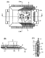
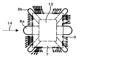
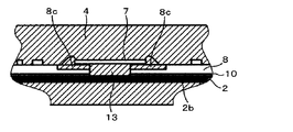
- FIG. 11 shows an electronic circuit assembly for controlling a transmission and a drive unit of an automobile, a base for fixing the electronic circuit assembly, and lead terminals electrically connected to the electronic circuit assembly. It is the electronic circuit device 1 sealed with.
- FIGS. 11B and 11C are partial cross-sectional views taken along lines II and II-II in FIG. 11A, respectively.
- An electronic circuit assembly 5 including a circuit board 8 on which the circuit element 6 and the bare chip 7 are mounted is bonded and fixed to the base 2 having the flange portion 2a with an adhesive 10 such as epoxy.
- the lead terminal 3 is disposed so as to correspond to the bonding pad portion 12 of the electronic circuit assembly 5.
- the electronic circuit assembly 5 and the lead terminal 3 are electrically connected to the bonding pad portion 12 included in the electronic circuit assembly 5 and the bonding pad portion 3a included in the lead terminal 3 through the fine aluminum wire 11 by wire bonding. .
- the electronic circuit assembly 5 is bonded and fixed to the upper surface of the base 2 with an adhesive 10
- the electronic circuit assembly 5 and the lead terminal 3 are connected with the aluminum thin wire 11, and then these components, circuit element 6, bare chip 7, and circuit board are connected.
- the base 2 and the lead terminal 3 are collectively embedded in the sealing resin 4 except for a part of the lead terminal 3 and a part of the flange portion 2a of the base 2.
- the sealing resin 4 is manufactured by transfer molding.
- thermosetting resin such as an epoxy resin
- the resin is fluidized and solidified in the mold.
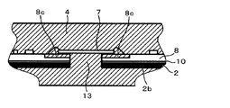
- the bare chip 7 is joined to the circuit board 8 by solder and silver paste material, and is electrically connected to the circuit board 8 by Au fine wires 9.
- a ceramic substrate having a high thermal conductivity is used as the circuit board 8. The heat generated in the bare chip 7 is transferred through the path radiated from the sealing resin 4 in close contact with the bare chip 7, the circuit board 8 on which the bare chip 7 is mounted, the substrate bonding portion 2 b, and the base 2. The heat is radiated to the mating member via the flange portion 2a.
- the structure of the conventional electronic circuit device is expensive because a ceramic substrate having high thermal conductivity is used for the circuit board in order to obtain high heat dissipation.
- a method of using a glass epoxy substrate as a circuit board but the glass epoxy substrate has a lower thermal conductivity than a ceramic substrate. The heat generated in the bare chip is transferred through the path where heat is released from the sealing resin that is in close contact with the bare chip, the circuit board on which the bare chip is mounted, the substrate bonding part, and the base, and is integrated with the base.
- an electronic circuit assembly for controlling a transmission and a drive unit of an automobile, a base for fixing the electronic circuit assembly, and a lead terminal electrically connected to the electronic circuit assembly are molded resin.
- a heat dissipation structure having an opening penetrating a circuit board and a base below a heat generating circuit element (bare chip), wherein both surfaces of the heat generating element are thermally connected to a sealing resin It was.
- the heat generating circuit element (bare chip) has an opening that penetrates the circuit board and the base, and both surfaces of the heat generating element are thermally connected to the sealing resin.
- the heat generated in the bare chip is transferred to the base via the sealing resin with high thermal conductivity instead of passing through the glass epoxy substrate with poor thermal conductivity, and the counterpart through the flange. Heat can be radiated to the member.
- heat dissipation can be improved at low cost by using sealing resin as a heat conductive material instead of a heat sink.
- the sealing resin can be injected into the opening that penetrates the circuit board and the base below the bare chip during transfer molding.
- the fluidity is improved, the generation of voids at the bottom of the bare chip can be reduced, and the sealing resin can be efficiently and thermally connected to both surfaces of the bare chip.
- FIG. 1 is a heat dissipation structure for an electronic circuit device according to a first embodiment.
- FIG. 5 is a detailed cross-sectional view of a heat dissipation structure of Example 2.
- FIG. 5 is a detailed cross-sectional view of a heat dissipation structure of Example 3.
- paths of the diagonal direction which it has in a circuit board.
- FIG. 3 is a detailed view of an opening for a passage combining a perpendicular direction and an oblique direction of the circuit board.
- FIG. 7 is a heat dissipation structure for an electronic circuit device according to a fourth embodiment.
- FIG. 6 is a detailed cross-sectional view of a heat dissipation structure of Example 4.
- FIG. 6 is an opening cross-sectional view for a groove-shaped passage included in a circuit board of Example 4; Conventional electronic circuit device heat dissipation structure.
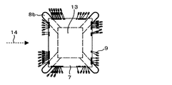
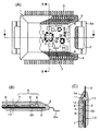
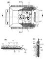
- FIGS. 1 and 8 show an electronic circuit assembly for controlling a transmission and a drive unit of an automobile, a base for fixing the electronic circuit assembly, and lead terminals electrically connected to the electronic circuit assembly.
- 1 is an electronic circuit device 1 sealed with a mold resin.
- 2, 3 and 9 are detailed views of the bare chip 7 part.
- the sectional view is a partial sectional view taken along line III-III.
- 4 to 6 are detailed views of the passage openings 8a and 8b provided in the circuit board 8
- FIGS. 7 and 10 are detailed views of the groove-shaped openings 8c.
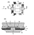
- FIG. 1 shows a first embodiment of the present invention.
- 1B and 1C are partial cross-sectional views taken along lines II and II-II of FIG. 1A, respectively.
- an electronic circuit assembly 5 comprising a circuit board 8 on which a circuit element 6 and a bare chip 7 are mounted is bonded and fixed to a base 2 having a flange portion 2a with an adhesive 10 such as epoxy.
- the lead terminal 3 is disposed so as to correspond to the bonding pad portion 12 of the electronic circuit assembly 5.
- the electronic circuit assembly 5 and the lead terminal 3 are electrically connected to the bonding pad portion 12 included in the electronic circuit assembly 5 and the bonding pad portion 3a included in the lead terminal 3 through the fine aluminum wire 11 by wire bonding. .
- the electronic circuit assembly 5 and the lead terminal 3 are connected with the aluminum thin wire 11, and then these components, circuit element 6, bare chip 7, and circuit board are connected.
- the base 2 and the lead terminal 3 are collectively embedded in the sealing resin 4 except for a part of the lead terminal 3 and a part of the flange portion 2a of the base 2.
- the sealing resin 4 is manufactured by transfer molding. Generally, a thermosetting resin such as an epoxy resin is used as the sealing resin, and the resin is fluidized and solidified in the mold.
- the bare chip 7 is joined to the circuit board 8 by solder and silver paste material, and is electrically connected to the circuit board 8 by Au fine wires 9.
- the circuit board 8 is a glass epoxy board.
- An opening 13 that penetrates the circuit board 8 and the base 2 is provided below the bare chip 7, and both surfaces of the bare chip 7 are in close contact with the sealing resin 4.
- the heat generated in the bare chip 7 is radiated from the sealing resin 4 that is in close contact with both surfaces of the bare chip 7. Further, heat is transmitted through the base 2 that is in close contact with the sealing resin 4 and is radiated to the mating member through the flange portion 2a.
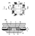
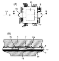
- FIG. 2 shows a second embodiment of the present invention.
- FIG. 2B is a partial cross-sectional view taken along the line III-III in FIG.
- a passage that passes through the circuit board 8 in a direction perpendicular to the flow direction 14 of the resin.
- Has an opening 8a for transfer improves the fluidity of the sealing resin 4 to the opening 13 penetrating the circuit board 8 and the base 2 under the bare chip 7 during transfer molding, and reduces the generation of voids under the bare chip 7
- the sealing resin 4 is efficiently and thermally coupled to both surfaces of the bare chip 7.
- the passage opening may be a passage opening 8b penetrating in an oblique direction with respect to the resin flow direction 14, as shown in FIG.
- the flowability of the resin may be further improved by combining the passage opening 8 a penetrating in the orthogonal direction and the passage opening 8 b penetrating in the oblique direction.
- path which has in the circuit board 8 may be the groove-shaped channel
- FIG. 3 shows a third embodiment of the present invention.
- FIG. 3B is a partial cross-sectional view taken along line III-III in FIG.
- the circuit board 8 and the base 2 are perpendicular to the resin flow direction 14. It has openings 8a and 2c for the passages that pass through, and improves the fluidity of the sealing resin 4 to the opening 13 that penetrates the circuit board 8 and the base 2 below the bare chip 7 at the time of transfer molding.
- the generation of voids can be reduced, and the sealing resin 4 is efficiently and thermally connected to both surfaces of the bare chip 7.
- the passage opening may be a passage opening 8b penetrating in an oblique direction with respect to the resin flow direction 14, as shown in FIG.
- the flowability of the resin may be further improved by combining the passage opening 8 a penetrating in the orthogonal direction and the passage opening 8 b penetrating in the oblique direction. .
- FIG. 8 shows a fourth embodiment of the present invention.
- 8B and 8C are partial cross-sectional views taken along lines II and II-II of FIG. 8A, respectively.
- an electronic circuit assembly 5 including a circuit board 8 on which a circuit element 6 and a bare chip 7 are mounted is bonded and fixed to a base 2 having a flange portion 2b with an adhesive 10 such as epoxy.
- the lead terminal 3 is disposed so as to correspond to the bonding pad portion 12 of the electronic circuit assembly 5.
- the electronic circuit assembly 5 and the lead terminal 3 are electrically connected to the bonding pad portion 12 included in the electronic circuit assembly 5 and the bonding pad portion 3a included in the lead terminal 3 through the fine aluminum wire 11 by wire bonding. .
- the electronic circuit assembly 5 and the lead terminal 3 are connected with the aluminum thin wire 11, and then these components, circuit element 6, bare chip 7, and circuit board are connected.
- the base 2 and the lead terminal 3 are collectively embedded in the sealing resin 4 except for a part of the lead terminal 3 and a part of the flange portion 2a of the base 2.
- the sealing resin 4 is manufactured by transfer molding. Generally, a thermosetting resin such as an epoxy resin is used as the sealing resin, and the resin is fluidized and solidified in the mold.
- the bare chip 7 is joined to the circuit board 8 by solder and silver paste material, and is electrically connected to the circuit board 8 by Au fine wires 9.
- the circuit board 8 is a glass epoxy board. An opening 13 that penetrates the circuit board 8 is provided below the bare chip 7, and both surfaces of the bare chip 7 are in close contact with the sealing resin 4. The heat generated in the bare chip 7 is radiated from the sealing resin 4 that is in close contact with both surfaces of the bare chip 7. Further, heat is transmitted through the base 2 that is in close contact with the sealing resin 4, and heat is radiated to the mating member through the flange portion 2a integrated with the base. As shown in FIG. 9, in order to make it easy to fill the sealing resin 4 in the opening 13 penetrating the circuit board 8 and the base 2, the circuit board 8 is used for a passage penetrating in the direction perpendicular to the resin flow direction 14.
- FIG. 9B is a partial cross-sectional view taken along the line II of FIG. 9A. Further, as shown in FIGS.
- the flowability of the resin may be further improved by combining the passage opening 8 a penetrating in the orthogonal direction and the passage opening 8 b penetrating in the oblique direction.
- path which has in the circuit board 8 may be the groove-shaped channel
Landscapes
- Engineering & Computer Science (AREA)
- Microelectronics & Electronic Packaging (AREA)
- General Engineering & Computer Science (AREA)
- Manufacturing & Machinery (AREA)
- Mechanical Engineering (AREA)
- Structures Or Materials For Encapsulating Or Coating Semiconductor Devices Or Solid State Devices (AREA)
- Cooling Or The Like Of Semiconductors Or Solid State Devices (AREA)
- Control Of Transmission Device (AREA)
Priority Applications (2)
| Application Number | Priority Date | Filing Date | Title |
|---|---|---|---|
| US13/985,235 US20130329384A1 (en) | 2011-03-01 | 2012-02-21 | Transmission Control Device and Electronic Circuit Device |
| DE112012001049.3T DE112012001049B4 (de) | 2011-03-01 | 2012-02-21 | Getriebesteuervorrichtung und elektronische Schaltungsvorrichtung |
Applications Claiming Priority (2)
| Application Number | Priority Date | Filing Date | Title |
|---|---|---|---|
| JP2011043464A JP5699006B2 (ja) | 2011-03-01 | 2011-03-01 | 変速機制御装置及び電子回路装置 |
| JP2011-043464 | 2011-03-01 |
Publications (1)
| Publication Number | Publication Date |
|---|---|
| WO2012117899A1 true WO2012117899A1 (ja) | 2012-09-07 |
Family
ID=46757838
Family Applications (1)
| Application Number | Title | Priority Date | Filing Date |
|---|---|---|---|
| PCT/JP2012/054162 Ceased WO2012117899A1 (ja) | 2011-03-01 | 2012-02-21 | 変速機制御装置及び電子回路装置 |
Country Status (4)
| Country | Link |
|---|---|
| US (1) | US20130329384A1 (https=) |
| JP (1) | JP5699006B2 (https=) |
| DE (1) | DE112012001049B4 (https=) |
| WO (1) | WO2012117899A1 (https=) |
Cited By (1)
| Publication number | Priority date | Publication date | Assignee | Title |
|---|---|---|---|---|
| DE102022210525A1 (de) | 2022-10-05 | 2024-04-11 | Vitesco Technologies Germany Gmbh | Elektronische Baugruppe, sowie Verfahren zu deren Herstellung |
Families Citing this family (3)
| Publication number | Priority date | Publication date | Assignee | Title |
|---|---|---|---|---|
| US8207607B2 (en) * | 2007-12-14 | 2012-06-26 | Denso Corporation | Semiconductor device with resin mold |
| KR20230023834A (ko) * | 2020-12-09 | 2023-02-20 | 주식회사 솔루엠 | 에어포켓 방지 기판, 에어포켓 방지 기판 모듈, 이를 포함하는 전기기기 및 이를 포함하는 전기기기의 제조 방법 |
| USD984397S1 (en) * | 2021-03-16 | 2023-04-25 | Yidong Cai | Circuit board |
Citations (3)
| Publication number | Priority date | Publication date | Assignee | Title |
|---|---|---|---|---|
| JPH03138952A (ja) * | 1989-10-25 | 1991-06-13 | Hitachi Ltd | 半導体デバイス |
| JP2000286379A (ja) * | 1999-01-28 | 2000-10-13 | Fujitsu Ltd | 半導体装置及びその製造方法 |
| JP2007043196A (ja) * | 2006-10-10 | 2007-02-15 | Hitachi Ltd | 電子回路装置 |
Family Cites Families (6)
| Publication number | Priority date | Publication date | Assignee | Title |
|---|---|---|---|---|
| US6188579B1 (en) * | 1999-07-12 | 2001-02-13 | Lucent Technologies Inc. | Apparatus and methods for forming a printed wiring board assembly to reduce pallet warpage |
| US6400574B1 (en) * | 2000-05-11 | 2002-06-04 | Micron Technology, Inc. | Molded ball grid array |
| JP3553513B2 (ja) | 2001-03-06 | 2004-08-11 | 株式会社日立製作所 | 自動車用電子回路装置 |
| DE10210041B4 (de) * | 2002-03-07 | 2009-04-16 | Continental Automotive Gmbh | Wärmeableitvorrichtung zum Ableiten von Wärme, die von einem elektrischen Bauelement erzeugt wird und Verfahren zum Herstellen einer derartigen Wärmeableitvorrichtung |
| JP4283514B2 (ja) * | 2002-09-24 | 2009-06-24 | 株式会社日立製作所 | 電子回路装置 |
| JP4821537B2 (ja) * | 2006-09-26 | 2011-11-24 | 株式会社デンソー | 電子制御装置 |
-
2011
- 2011-03-01 JP JP2011043464A patent/JP5699006B2/ja not_active Expired - Fee Related
-
2012
- 2012-02-21 DE DE112012001049.3T patent/DE112012001049B4/de not_active Withdrawn - After Issue
- 2012-02-21 US US13/985,235 patent/US20130329384A1/en not_active Abandoned
- 2012-02-21 WO PCT/JP2012/054162 patent/WO2012117899A1/ja not_active Ceased
Patent Citations (3)
| Publication number | Priority date | Publication date | Assignee | Title |
|---|---|---|---|---|
| JPH03138952A (ja) * | 1989-10-25 | 1991-06-13 | Hitachi Ltd | 半導体デバイス |
| JP2000286379A (ja) * | 1999-01-28 | 2000-10-13 | Fujitsu Ltd | 半導体装置及びその製造方法 |
| JP2007043196A (ja) * | 2006-10-10 | 2007-02-15 | Hitachi Ltd | 電子回路装置 |
Cited By (1)
| Publication number | Priority date | Publication date | Assignee | Title |
|---|---|---|---|---|
| DE102022210525A1 (de) | 2022-10-05 | 2024-04-11 | Vitesco Technologies Germany Gmbh | Elektronische Baugruppe, sowie Verfahren zu deren Herstellung |
Also Published As
| Publication number | Publication date |
|---|---|
| US20130329384A1 (en) | 2013-12-12 |
| DE112012001049B4 (de) | 2016-04-07 |
| JP2012182267A (ja) | 2012-09-20 |
| DE112012001049T5 (de) | 2013-12-12 |
| JP5699006B2 (ja) | 2015-04-08 |
Similar Documents
| Publication | Publication Date | Title |
|---|---|---|
| KR101643332B1 (ko) | 초음파 웰딩을 이용한 클립 본딩 반도체 칩 패키지 및 그 제조 방법 | |
| CN104051377B (zh) | 功率覆盖结构及其制作方法 | |
| CN105405815A (zh) | 半导体装置及其制造方法 | |
| WO2019146402A1 (ja) | 電力変換装置及び電力変換装置の製造方法 | |
| JP5607829B2 (ja) | 半導体装置 | |
| CN103094451A (zh) | Led模块及其接合方法 | |
| JP5120032B2 (ja) | 電子装置 | |
| JP5262983B2 (ja) | モールドパッケージおよびその製造方法 | |
| JP5699006B2 (ja) | 変速機制御装置及び電子回路装置 | |
| JP7088224B2 (ja) | 半導体モジュールおよびこれに用いられる半導体装置 | |
| JP6797002B2 (ja) | 半導体装置および半導体装置の製造方法 | |
| JP2008205100A (ja) | 電力半導体装置 | |
| CN114730748B (zh) | 用于消耗装置的可控电功率供应的具有被封装的功率半导体的功率模块及用于生产该功率模块的方法 | |
| WO2015132969A1 (ja) | 絶縁基板及び半導体装置 | |
| WO2020189508A1 (ja) | 半導体モジュールおよびこれに用いられる半導体装置 | |
| CN104134633A (zh) | 大功率芯片柔性基板封装结构及封装工艺 | |
| JP6354163B2 (ja) | 回路基板および電子装置 | |
| JP5239736B2 (ja) | 電子装置 | |
| JP2014216326A (ja) | 電子装置およびその製造方法 | |
| KR20150031029A (ko) | 반도체 패키지 및 그 제조 방법 | |
| JP2008141140A (ja) | 半導体装置 | |
| JP2013149876A (ja) | パッケージオンパッケージ型半導体装置およびパッケージオンパッケージ型半導体装置の製造方法 | |
| CN109792848B (zh) | 用于变速箱控制模块的电子组件和其制造方法 | |
| JP2016092261A (ja) | 電子制御装置およびその製造方法 | |
| JP2019114759A (ja) | 回路モジュール、回路モジュールの製造方法 |
Legal Events
| Date | Code | Title | Description |
|---|---|---|---|
| 121 | Ep: the epo has been informed by wipo that ep was designated in this application |
Ref document number: 12752192 Country of ref document: EP Kind code of ref document: A1 |
|
| WWE | Wipo information: entry into national phase |
Ref document number: 13985235 Country of ref document: US |
|
| WWE | Wipo information: entry into national phase |
Ref document number: 1120120010493 Country of ref document: DE Ref document number: 112012001049 Country of ref document: DE |
|
| 122 | Ep: pct application non-entry in european phase |
Ref document number: 12752192 Country of ref document: EP Kind code of ref document: A1 |