WO2012117745A1 - 半導体基板及びその製造方法 - Google Patents
半導体基板及びその製造方法 Download PDFInfo
- Publication number
- WO2012117745A1 WO2012117745A1 PCT/JP2012/001477 JP2012001477W WO2012117745A1 WO 2012117745 A1 WO2012117745 A1 WO 2012117745A1 JP 2012001477 W JP2012001477 W JP 2012001477W WO 2012117745 A1 WO2012117745 A1 WO 2012117745A1
- Authority
- WO
- WIPO (PCT)
- Prior art keywords
- layer
- crystal layer
- semiconductor layer
- semiconductor
- field effect
- Prior art date
- Legal status (The legal status is an assumption and is not a legal conclusion. Google has not performed a legal analysis and makes no representation as to the accuracy of the status listed.)
- Ceased
Links
Images










Classifications
-
- H—ELECTRICITY
- H10—SEMICONDUCTOR DEVICES; ELECTRIC SOLID-STATE DEVICES NOT OTHERWISE PROVIDED FOR
- H10D—INORGANIC ELECTRIC SEMICONDUCTOR DEVICES
- H10D30/00—Field-effect transistors [FET]
- H10D30/60—Insulated-gate field-effect transistors [IGFET]
- H10D30/67—Thin-film transistors [TFT]
- H10D30/674—Thin-film transistors [TFT] characterised by the active materials
- H10D30/675—Group III-V materials, Group II-VI materials, Group IV-VI materials, selenium or tellurium
-
- H—ELECTRICITY
- H10—SEMICONDUCTOR DEVICES; ELECTRIC SOLID-STATE DEVICES NOT OTHERWISE PROVIDED FOR
- H10P—GENERIC PROCESSES OR APPARATUS FOR THE MANUFACTURE OR TREATMENT OF DEVICES COVERED BY CLASS H10
- H10P10/00—Bonding of wafers, substrates or parts of devices
-
- H—ELECTRICITY
- H10—SEMICONDUCTOR DEVICES; ELECTRIC SOLID-STATE DEVICES NOT OTHERWISE PROVIDED FOR
- H10D—INORGANIC ELECTRIC SEMICONDUCTOR DEVICES
- H10D10/00—Bipolar junction transistors [BJT]
- H10D10/01—Manufacture or treatment
-
- H—ELECTRICITY
- H10—SEMICONDUCTOR DEVICES; ELECTRIC SOLID-STATE DEVICES NOT OTHERWISE PROVIDED FOR
- H10D—INORGANIC ELECTRIC SEMICONDUCTOR DEVICES
- H10D30/00—Field-effect transistors [FET]
- H10D30/01—Manufacture or treatment
- H10D30/015—Manufacture or treatment of FETs having heterojunction interface channels or heterojunction gate electrodes, e.g. HEMT
-
- H—ELECTRICITY
- H10—SEMICONDUCTOR DEVICES; ELECTRIC SOLID-STATE DEVICES NOT OTHERWISE PROVIDED FOR
- H10D—INORGANIC ELECTRIC SEMICONDUCTOR DEVICES
- H10D30/00—Field-effect transistors [FET]
- H10D30/01—Manufacture or treatment
- H10D30/021—Manufacture or treatment of FETs having insulated gates [IGFET]
- H10D30/031—Manufacture or treatment of FETs having insulated gates [IGFET] of thin-film transistors [TFT]
-
- H—ELECTRICITY
- H10—SEMICONDUCTOR DEVICES; ELECTRIC SOLID-STATE DEVICES NOT OTHERWISE PROVIDED FOR
- H10D—INORGANIC ELECTRIC SEMICONDUCTOR DEVICES
- H10D30/00—Field-effect transistors [FET]
- H10D30/40—FETs having zero-dimensional [0D], one-dimensional [1D] or two-dimensional [2D] charge carrier gas channels
- H10D30/47—FETs having zero-dimensional [0D], one-dimensional [1D] or two-dimensional [2D] charge carrier gas channels having two-dimensional [2D] charge carrier gas channels, e.g. nanoribbon FETs or high electron mobility transistors [HEMT]
- H10D30/471—High electron mobility transistors [HEMT] or high hole mobility transistors [HHMT]
- H10D30/473—High electron mobility transistors [HEMT] or high hole mobility transistors [HHMT] having confinement of carriers by multiple heterojunctions, e.g. quantum well HEMT
- H10D30/4732—High electron mobility transistors [HEMT] or high hole mobility transistors [HHMT] having confinement of carriers by multiple heterojunctions, e.g. quantum well HEMT using Group III-V semiconductor material
-
- H—ELECTRICITY
- H10—SEMICONDUCTOR DEVICES; ELECTRIC SOLID-STATE DEVICES NOT OTHERWISE PROVIDED FOR
- H10D—INORGANIC ELECTRIC SEMICONDUCTOR DEVICES
- H10D30/00—Field-effect transistors [FET]
- H10D30/40—FETs having zero-dimensional [0D], one-dimensional [1D] or two-dimensional [2D] charge carrier gas channels
- H10D30/47—FETs having zero-dimensional [0D], one-dimensional [1D] or two-dimensional [2D] charge carrier gas channels having two-dimensional [2D] charge carrier gas channels, e.g. nanoribbon FETs or high electron mobility transistors [HEMT]
- H10D30/471—High electron mobility transistors [HEMT] or high hole mobility transistors [HHMT]
- H10D30/475—High electron mobility transistors [HEMT] or high hole mobility transistors [HHMT] having wider bandgap layer formed on top of lower bandgap active layer, e.g. undoped barrier HEMTs such as i-AlGaN/GaN HEMTs
-
- H—ELECTRICITY
- H10—SEMICONDUCTOR DEVICES; ELECTRIC SOLID-STATE DEVICES NOT OTHERWISE PROVIDED FOR
- H10D—INORGANIC ELECTRIC SEMICONDUCTOR DEVICES
- H10D30/00—Field-effect transistors [FET]
- H10D30/60—Insulated-gate field-effect transistors [IGFET]
-
- H—ELECTRICITY
- H10—SEMICONDUCTOR DEVICES; ELECTRIC SOLID-STATE DEVICES NOT OTHERWISE PROVIDED FOR
- H10D—INORGANIC ELECTRIC SEMICONDUCTOR DEVICES
- H10D62/00—Semiconductor bodies, or regions thereof, of devices having potential barriers
- H10D62/80—Semiconductor bodies, or regions thereof, of devices having potential barriers characterised by the materials
- H10D62/85—Semiconductor bodies, or regions thereof, of devices having potential barriers characterised by the materials being Group III-V materials, e.g. GaAs
- H10D62/8503—Nitride Group III-V materials, e.g. AlN or GaN
-
- H—ELECTRICITY
- H10—SEMICONDUCTOR DEVICES; ELECTRIC SOLID-STATE DEVICES NOT OTHERWISE PROVIDED FOR
- H10P—GENERIC PROCESSES OR APPARATUS FOR THE MANUFACTURE OR TREATMENT OF DEVICES COVERED BY CLASS H10
- H10P14/00—Formation of materials, e.g. in the shape of layers or pillars
- H10P14/20—Formation of materials, e.g. in the shape of layers or pillars of semiconductor materials
-
- H—ELECTRICITY
- H10—SEMICONDUCTOR DEVICES; ELECTRIC SOLID-STATE DEVICES NOT OTHERWISE PROVIDED FOR
- H10P—GENERIC PROCESSES OR APPARATUS FOR THE MANUFACTURE OR TREATMENT OF DEVICES COVERED BY CLASS H10
- H10P90/00—Preparation of wafers not covered by a single main group of this subclass, e.g. wafer reinforcement
- H10P90/19—Preparing inhomogeneous wafers
- H10P90/1904—Preparing vertically inhomogeneous wafers
- H10P90/1906—Preparing SOI wafers
- H10P90/1914—Preparing SOI wafers using bonding
-
- H—ELECTRICITY
- H10—SEMICONDUCTOR DEVICES; ELECTRIC SOLID-STATE DEVICES NOT OTHERWISE PROVIDED FOR
- H10P—GENERIC PROCESSES OR APPARATUS FOR THE MANUFACTURE OR TREATMENT OF DEVICES COVERED BY CLASS H10
- H10P90/00—Preparation of wafers not covered by a single main group of this subclass, e.g. wafer reinforcement
- H10P90/19—Preparing inhomogeneous wafers
- H10P90/1904—Preparing vertically inhomogeneous wafers
- H10P90/1906—Preparing SOI wafers
- H10P90/1914—Preparing SOI wafers using bonding
- H10P90/1916—Preparing SOI wafers using bonding with separation or delamination along an ion implanted layer, e.g. Smart-cut
-
- H—ELECTRICITY
- H10—SEMICONDUCTOR DEVICES; ELECTRIC SOLID-STATE DEVICES NOT OTHERWISE PROVIDED FOR
- H10P—GENERIC PROCESSES OR APPARATUS FOR THE MANUFACTURE OR TREATMENT OF DEVICES COVERED BY CLASS H10
- H10P90/00—Preparation of wafers not covered by a single main group of this subclass, e.g. wafer reinforcement
- H10P90/19—Preparing inhomogeneous wafers
- H10P90/1904—Preparing vertically inhomogeneous wafers
- H10P90/1906—Preparing SOI wafers
- H10P90/1922—Preparing SOI wafers using silicon etch back techniques, e.g. BESOI or ELTRAN
-
- H—ELECTRICITY
- H10—SEMICONDUCTOR DEVICES; ELECTRIC SOLID-STATE DEVICES NOT OTHERWISE PROVIDED FOR
- H10W—GENERIC PACKAGES, INTERCONNECTIONS, CONNECTORS OR OTHER CONSTRUCTIONAL DETAILS OF DEVICES COVERED BY CLASS H10
- H10W10/00—Isolation regions in semiconductor bodies between components of integrated devices
- H10W10/10—Isolation regions comprising dielectric materials
- H10W10/181—Semiconductor-on-insulator [SOI] isolation regions, e.g. buried oxide regions of SOI wafers
-
- H—ELECTRICITY
- H10—SEMICONDUCTOR DEVICES; ELECTRIC SOLID-STATE DEVICES NOT OTHERWISE PROVIDED FOR
- H10D—INORGANIC ELECTRIC SEMICONDUCTOR DEVICES
- H10D30/00—Field-effect transistors [FET]
- H10D30/40—FETs having zero-dimensional [0D], one-dimensional [1D] or two-dimensional [2D] charge carrier gas channels
- H10D30/47—FETs having zero-dimensional [0D], one-dimensional [1D] or two-dimensional [2D] charge carrier gas channels having two-dimensional [2D] charge carrier gas channels, e.g. nanoribbon FETs or high electron mobility transistors [HEMT]
-
- H—ELECTRICITY
- H10—SEMICONDUCTOR DEVICES; ELECTRIC SOLID-STATE DEVICES NOT OTHERWISE PROVIDED FOR
- H10D—INORGANIC ELECTRIC SEMICONDUCTOR DEVICES
- H10D62/00—Semiconductor bodies, or regions thereof, of devices having potential barriers
- H10D62/80—Semiconductor bodies, or regions thereof, of devices having potential barriers characterised by the materials
- H10D62/85—Semiconductor bodies, or regions thereof, of devices having potential barriers characterised by the materials being Group III-V materials, e.g. GaAs
- H10D62/852—Semiconductor bodies, or regions thereof, of devices having potential barriers characterised by the materials being Group III-V materials, e.g. GaAs being Group III-V materials comprising three or more elements, e.g. AlGaN or InAsSbP
-
- H—ELECTRICITY
- H10—SEMICONDUCTOR DEVICES; ELECTRIC SOLID-STATE DEVICES NOT OTHERWISE PROVIDED FOR
- H10D—INORGANIC ELECTRIC SEMICONDUCTOR DEVICES
- H10D64/00—Electrodes of devices having potential barriers
- H10D64/60—Electrodes characterised by their materials
- H10D64/66—Electrodes having a conductor capacitively coupled to a semiconductor by an insulator, e.g. MIS electrodes
- H10D64/68—Electrodes having a conductor capacitively coupled to a semiconductor by an insulator, e.g. MIS electrodes characterised by the insulator, e.g. by the gate insulator
- H10D64/691—Electrodes having a conductor capacitively coupled to a semiconductor by an insulator, e.g. MIS electrodes characterised by the insulator, e.g. by the gate insulator comprising metallic compounds, e.g. metal oxides or metal silicates
Definitions
- the present invention relates to a semiconductor substrate, a field effect transistor, a semiconductor substrate manufacturing method, and a field effect transistor manufacturing method.
- this application is NEDO, “Nanoelectronics semiconductor new material / new structure nanoelectronic device technology development-Research and development of III-V semiconductor channel transistor technology on silicon platform”, commissioned research, Article 19 of Industrial Technology Strengthening Act, 2009 Is a patent application subject to
- III-V MISFET Metal-Insulator-Semiconductor-Field-Effect-Transistor
- III-V compound semiconductor layer has high electron mobility and is expected as a switching device suitable for high frequency operation and high power operation. ing.
- the III-V MISFET is promising as an alternative element to Si-CMOSFET (Complementary Metal-Oxide-Semiconductor-Field-Effect-Transistor) using silicon as a channel material.
- CMOSFET Complementary Metal-Oxide-Semiconductor-Field-Effect-Transistor
- III-V group MISFETs are formed on a silicon substrate, considering that existing manufacturing equipment and existing processes can be used. It is preferable.
- Non-Patent Documents 1 and 2 describe MISFETs that use a III-V compound semiconductor layer as a channel layer. In addition, for example, it is effective to treat the surface of a compound semiconductor with a sulfide in order to reduce the energy level (referred to as “interface level” in this specification) formed at the interface between the semiconductor and the insulator. Is described in Non-Patent Document 3.
- Non-Patent Document 1 Ren, F. et al. Demonstration of enhancement-mode p- and n-channel GaAs MOSFETs with Ga 2 O 3 (Gd 2 O 3 ) As gate oxide. Solid State Electron. 41, 1751-1753 (1997 ).
- Non-Patent Document 2 Chin, H. C. et al.
- Non-Patent Document 3 S.Arabasz, et al., Vac. 80 (2006), 888 pages
- III-V group MISFET In order to manufacture a III-V group MISFET on a silicon substrate, it is necessary to form a III-V group compound semiconductor layer on the silicon substrate. However, since the lattice mismatch between the group III-V compound semiconductor layer and the silicon substrate is large, it is difficult to form a high-quality group III-V compound semiconductor layer by epitaxial crystal growth.
- a III-V compound semiconductor layer is formed on a silicon substrate by using a DWB (direct wafer bonding) method known as an optical device integration technique, that is, a method of directly bonding substrates. It is done.
- a DWB method direct wafer bonding method known as an optical device integration technique, that is, a method of directly bonding substrates. It is done.
- the silicon substrate and the group III-V compound semiconductor layer are bonded to each other, so that damage such as generation of crystal defects may be applied to the group III-V compound semiconductor layer. If the damage exceeds the allowable damage when the III-V compound semiconductor layer is used as the channel layer of the MISFET, the III-V compound semiconductor layer is used as the channel layer of the MISFET. It becomes difficult to use.
- damage to the III-V compound semiconductor layer becomes more significant.
- a base substrate, a first insulator layer, and a semiconductor layer are included, and the base substrate, the first insulator layer, and the semiconductor layer are a base substrate,
- the first insulator layer is located in the order of the semiconductor layer
- the first insulator layer is made of amorphous metal oxide or amorphous metal nitride
- the semiconductor layer includes the first crystal layer and the second crystal layer
- the first crystal layer and the second crystal layer are located in this order from the base substrate side in the order of the first crystal layer and the second crystal layer
- the electron affinity E a1 of the first crystal layer is the electron affinity E of the second crystal layer.
- a semiconductor substrate larger than a2 is provided.
- the semiconductor layer may further include a third crystal layer.
- the first crystal layer, the second crystal layer, and the third crystal layer are arranged from the base substrate side in the third crystal layer, the first crystal layer, the first crystal layer, Located in the order of two crystal layers, the electron affinity E a3 of the third crystal layer is smaller than the electron affinity E a1 of the first crystal layer.
- In x1 Ga 1-x1 As (0 ⁇ x1 ⁇ 1) can be exemplified as the first crystal layer
- In x2 Ga 1-x2 As (0 ⁇ x2 ⁇ 1) can be exemplified as the second crystal layer.
- In x3 Ga 1-x3 As (0 ⁇ x3 ⁇ 1) can be exemplified, and it is preferable to satisfy the relationship of x1> x2 and x1> x3.
- the thickness of the semiconductor layer is preferably 20 nm or less.
- a field effect transistor in a second aspect of the present invention, includes a source electrode and a drain electrode that are electrically connected to a semiconductor layer in the semiconductor substrate.
- the semiconductor layer has a source region in contact with the source electrode or a drain region in contact with the drain electrode.
- the source region or the drain region is selected from the group consisting of group III atoms and group V atoms constituting the semiconductor layer.
- An alloy of at least one kind of atom and a metal atom may be included.
- the metal atom is preferably a nickel atom.
- a semiconductor having a gate electrode on the side opposite to the base substrate of the semiconductor layer, and an interface located on the drain region side of the source region and an interface located on the source region side of the drain region sandwiched between the gate electrode and the base substrate It is preferably formed in a region under the gate electrode, which is a region of the layer.
- the source region or the drain region may further include donor impurity atoms.
- the source region or the drain region may further include acceptor impurity atoms.
- a semiconductor layer forming step of forming a semiconductor layer on the semiconductor layer forming substrate by an epitaxial crystal growth method, and forming a first insulator layer on the semiconductor layer by an atomic layer deposition method comprising: a first insulator layer forming step; a bonding step of bonding a base substrate on the first insulator layer; and a removing step of removing the semiconductor layer forming substrate from the semiconductor layer.
- a first step of forming a second crystal layer on the formation substrate by an epitaxial crystal growth method and after the first step, a first crystal layer having an electron affinity E a1 greater than the electron affinity E a2 of the second crystal layer, And a second step of forming the second crystal layer on the second crystal layer by an epitaxial crystal growth method.
- a third crystal layer having an electron affinity E a3 smaller than the electron affinity E a1 of the first crystal layer is formed on the first crystal layer by an epitaxial crystal growth method.
- a step may be further included.
- Manufacturing a field effect transistor comprising: forming a metal film in contact with a semiconductor layer; and heat-treating the metal film to form at least one of a source region and a drain region in a portion of the semiconductor layer in contact with the metal film.
- one or more conditions selected from the temperature and time of the heat treatment can be controlled, and the interface and drain region located on the drain region side of the source region can be controlled by controlling the conditions.
- the position of one or more interfaces selected from the interfaces located on the source region side can be controlled to be formed in a region under the gate electrode that is a region of the semiconductor layer sandwiched between the gate electrode and the base substrate.
- a cross section of a semiconductor substrate 100 is shown.
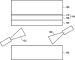
- a cross section in the manufacturing process of the semiconductor substrate 100 is shown.
- a cross section in the manufacturing process of the semiconductor substrate 100 is shown.
- a cross section in the manufacturing process of the semiconductor substrate 100 is shown.
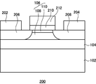
- a cross section of a field effect transistor 200 is shown.
- a cross section in the manufacturing process of the field effect transistor 200 is shown.
- a cross section in the manufacturing process of the field effect transistor 200 is shown.
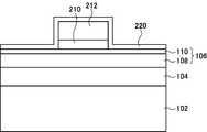
- a cross section in the manufacturing process of the field effect transistor 200 is shown.
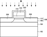
- a cross section in the manufacturing process of the field effect transistor 200 is shown.
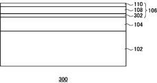
- a cross section of a semiconductor substrate 300 is shown.
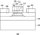
- a cross section of a field effect transistor 400 is shown.
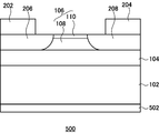
- a cross section of a field effect transistor 500 is shown.
- a cross section of a field effect transistor 600 is shown.
- the cross-sectional TEM photograph of the field effect transistor of Example 1 is shown.
- the Id-Vg characteristic of the field effect transistor of Example 1 is shown.
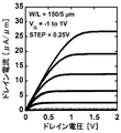
- the Id-Vd characteristic of the field effect transistor of Example 1 is shown.
- the mobility of the field effect transistor of Example 1 is shown.
- the Id-Vg characteristic of the field effect transistor of Example 1 is shown.
- the mobility of the field effect transistor of Example 1 is shown.
- the channel layer thickness dependence of the mobility of the field effect transistor of Example 1 is shown.
- the cross-sectional TEM photograph of the field effect transistor of Example 2 is shown.
- the Id-Vg characteristic of the field effect transistor of Example 2 is shown.
- the mobility of the field effect transistor of Example 2 is shown. 4 shows a cross-sectional TEM photograph of the field effect transistor of Example 3.
- FIG. 4 shows a cross-sectional TEM photograph of the field effect transistor of Example 3.
- the Id-Vg characteristic of the field effect transistor of Example 3 is shown.
- the Id-Vd characteristic of the field effect transistor of Example 3 is shown.
- the channel length dependence of the subthreshold (S.S.) value of a field effect transistor is shown.
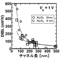
- the channel length dependence of the barrier lowering effect (DIBL) value by the drain voltage of a field effect transistor is shown.
- the channel length dependence of the threshold value (Vth) of the field effect transistor of Example 3 is shown.
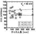
- the channel length dependence of SS value of the field effect transistor of Example 3 is shown.
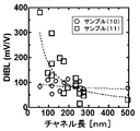
- the channel length dependence of the DIBL value of the field effect transistor of Example 3 is shown.
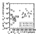
- the on-current / off-current characteristics of the field-effect transistor of Example 3 are shown.
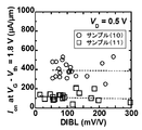
- the DIBL dependence of the on-state current of the field effect transistor of Example 3 is shown.
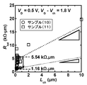
- the channel length dependence of the total resistance value of the field effect transistor of Example 3 is shown.
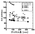
- the channel length dependence of the SS value of the field effect transistor in Example 3 and the reference example is shown.
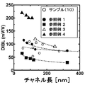
- the channel length dependence of the DIBL value of the field effect transistor in Example 3 and a reference example is shown.
- FIG. 1 shows a cross section of the semiconductor substrate 100.
- the semiconductor substrate 100 includes a base substrate 102, a first insulator layer 104, and a semiconductor layer 106.
- the base substrate 102, the first insulator layer 104, and the semiconductor layer 106 are positioned in the order of the base substrate 102, the first insulator layer 104, and the semiconductor layer 106.
- Examples of the base substrate 102 include a substrate whose surface is a silicon crystal.
- Examples of the substrate whose surface is a silicon crystal include a silicon substrate and an SOI (Silicon-on-Insulator) substrate, and an inexpensive silicon substrate is preferable in production.
- SOI Silicon-on-Insulator
- the base substrate 102 is not limited to a substrate whose surface is a silicon crystal, and may be an insulator substrate such as glass or ceramics, a conductor substrate such as metal, or a semiconductor substrate such as silicon carbide.
- the first insulator layer 104 is made of amorphous metal oxide or amorphous metal nitride.
- the semiconductor layer 106 is formed on the base substrate 102 with the first insulator layer 104 interposed therebetween by a bonding method. Therefore, it is desirable that the surface of the first insulator layer 104 be flat.
- the first insulator layer 104 is preferably made of a metal oxide or metal nitride formed by an atomic layer deposition method (ALD method), or SiO 2 formed by thermal oxidation.
- ALD method atomic layer deposition method
- SiO 2 formed by thermal oxidation.
- an index of surface flatness an RMS (Root Mean Square) value of surface roughness observed using an AFM (Atomic Force Microscope) can be used, and an RMS value of the surface of the first insulator layer 104 is 1 nm or less. Preferably there is.
- the first insulator layer 104 By forming the first insulator layer 104 by an atomic layer deposition method (ALD method), amorphous Al 2 O 3 , SiO 2 , AlN, AlON, HfO 2 , HfSiON, ZrO 2 , SiN x with a flat surface is formed.
- a first insulator layer 104 composed of one or more layers selected from (for example, Si 3 N 4 ) and Ta 2 O 5 can be formed. Further, by forming the first insulator layer 104 by a thermal oxidation method, amorphous SiO 2 having a flat surface can be formed.
- SiO 2 and Al 2 O 3 have high thermal stability
- the use of one or more insulating layers selected from SiO 2 and Al 2 O 3 for the first insulator layer 104 enables process resistance (later steps)
- the semiconductor substrate 100 of this example includes a first insulator layer 104 made of an amorphous metal oxide or an amorphous metal nitride between the base substrate 102 and the semiconductor layer 106. Since the first insulator layer 104 does not have a crystal structure, in the semiconductor substrate 100 of this example, the stress caused by the difference in lattice constant between the base substrate 102 and the semiconductor layer 106 is relaxed. Therefore, crystal defects are less likely to occur in the semiconductor layer 106. As described above, by disposing the amorphous first insulator layer 104 between the base substrate 102 and the semiconductor layer 106, damage to the semiconductor layer 106 in the manufacturing process can be reduced.
- the semiconductor layer 106 is made of a III-V group compound semiconductor. Since the semiconductor substrate 100 includes the semiconductor layer 106 made of a III-V group compound semiconductor, a high-performance MISFET with high mobility can be formed on the base substrate 102.
- the thickness of the semiconductor layer 106 is preferably within a range of 20 nm or less. By setting the thickness of the semiconductor layer 106 to 20 nm or less, a MISFET having an extremely thin film body can be configured. The MISFET having an extremely thin film body can suppress the short channel effect and reduce the leakage current.
- the thickness of the semiconductor layer 106 is more preferably 10 nm or less.
- the semiconductor layer 106 may be terminated with sulfur atoms on the surface in contact with the first insulator layer 104. In this case, the interface state density at the interface between the first insulator layer 104 and the semiconductor layer 106 can be reduced.
- the semiconductor layer 106 includes a first crystal layer 108 and a second crystal layer 110.
- the first crystal layer 108 and the second crystal layer 110 are located in the order of the first crystal layer 108 and the second crystal layer 110 from the base substrate 102 side.
- the first crystal layer 108 is lattice-matched or pseudo-lattice-matched to the second crystal layer 110.
- the electron affinity E a1 of the first crystal layer 108, to form a first crystal layer 108 and the second crystal layer 110 to be greater than the electron affinity E a2 of the second crystal layer 110.
- InGaAs or InAs can be exemplified as the first crystal layer 108, and InGaAsP can be exemplified as the second crystal layer 110 in this case.
- In x1 Ga 1-x1 As (0 ⁇ x1 ⁇ 1) can be exemplified as the first crystal layer 108.
- In x2 Ga 1-x2 As (0 ⁇ x2 ⁇ 1, x1> x2) is used as the second crystal layer 110.
- In x1 Ga 1-x1 As (0.53 ⁇ x1 ⁇ 1) can be exemplified as the first crystal layer 108.
- In x2 Ga 1-x2 As (0 ⁇ x2 ⁇ 0.53) is used as the second crystal layer 110.
- In 0.7 Ga 0.3 As can be exemplified as the first crystal layer 108.
- In 0.3 Ga 0.7 As can be exemplified as the second crystal layer 110.
- InAs can be exemplified as the first crystal layer 108, and In 0.3 Ga 0.7 As can be exemplified as the second crystal layer 110 in this case.
- the thickness of the first crystal layer 108 can be within a range of 10 nm or less, and particularly preferably within a range of 5 nm or less.
- the thickness of the second crystal layer 110 can be in the range of 10 nm or less, and is particularly preferably in the range of 2 nm to 5 nm. At least part of the second crystal layer 110 may be doped with impurities.
- FIG. 2 to 4 show cross sections in the process of manufacturing the semiconductor substrate 100.
- a semiconductor layer forming substrate 120 is prepared, and a semiconductor layer 106 is formed on the semiconductor layer forming substrate 120 by an epitaxial crystal growth method. Thereafter, the first insulator layer 104 is formed over the semiconductor layer 106 by an atomic layer deposition method.
- An example of the semiconductor layer forming substrate 120 is an InP substrate.
- the InP substrate As the semiconductor layer formation substrate 120, a high-quality III-V compound semiconductor layer 106 can be formed.
- the semiconductor layer 106 is formed by forming the second crystal layer 110 by the epitaxial crystal growth method and then forming the first crystal layer 108 by the epitaxial crystal growth method.
- the second crystal layer 110 and the first crystal layer 108 are formed so that the electron affinity E a1 of the first crystal layer 108 is larger than the electron affinity E a2 of the second crystal layer 110.
- an MOCVD (Metal Organic Chemical Vapor Deposition) method can be used for the formation of the semiconductor layer 106 by the epitaxial growth method.
- MOCVD method Metal Organic Chemical Vapor Deposition
- TMIn trimethylindium
- TMGa trimethylgallium
- AsH 3 arsine
- PH 3 phosphine
- Hydrogen can be used as the carrier gas.
- the reaction temperature can be appropriately selected in the range of 300 ° C. to 900 ° C., preferably in the range of 450 to 750 ° C.
- the thickness of the epitaxial growth layer can be controlled by appropriately selecting the reaction time.
- the first insulator layer 104 By forming the first insulator layer 104 by an atomic layer deposition method (ALD method), the first insulator layer 104 can be formed flat. Therefore, the first insulator layer 104 is formed between the first insulator layer 104 and the semiconductor layer 106. In addition, the damage to the semiconductor layer 106 can be reduced in the step of bonding the first insulator layer 104 and the base substrate 102 together. Details of the bonding step will be described later.
- ALD method atomic layer deposition method
- a base substrate 102 is prepared separately, and the surface of the first insulator layer 104 and the surface of the base substrate 102 are activated with an argon beam 122. After that, as shown in FIG. 4, the surface of the first insulator layer 104 activated by the argon beam 122 and the surface of the base substrate 102 are bonded and bonded. Bonding can be performed at room temperature. The activation need not be performed with the argon beam 122 but may be performed with a beam of other rare gas or the like. Thereafter, the semiconductor layer forming substrate 120 is removed by etching with an HCl solution or the like. In this way, the semiconductor substrate 100 shown in FIG. 1 can be manufactured.
- an insulating layer by an ALD method may be formed on the surface of the base substrate 102, and the insulating layer on the surface of the base substrate 102 may be bonded to the first insulator layer 104.
- a hydrophilic treatment can be performed before the surface of the insulating layer on the base substrate 102 and the surface of the first insulator layer 104 are bonded to each other.
- the hydrophilic treatment it is preferable to heat the base substrate 102 and the first insulator layer 104 after bonding.
- the surface of the semiconductor layer 106 may be subjected to sulfur termination between the formation of the semiconductor layer 106 and the formation of the first insulator layer 104.
- FIG. 5 shows a cross section of the field effect transistor 200.
- the field effect transistor 200 is formed using the semiconductor substrate 100 shown in FIG.
- the field effect transistor 200 includes a source electrode 202 and a drain electrode 204 on a semiconductor substrate 100.
- the source electrode 202 and the drain electrode 204 are electrically connected to the semiconductor layer 106 of the semiconductor substrate 100.
- the semiconductor layer 106 has a source region 206 and a drain region 208.
- Source region 206 is in contact with source electrode 202
- drain region 208 is in contact with drain electrode 204.
- the field effect transistor 200 includes a second insulator layer 210 on the other surface of the semiconductor layer 106 facing the surface where the semiconductor layer 106 and the first insulator layer 104 are in contact with each other.
- the second insulator layer 210 may be provided on a region of the semiconductor layer 106 that is sandwiched between the source region 206 and the drain region 208.
- the field effect transistor 200 includes a gate electrode 212 on the second insulator layer 210.
- a part of the second insulator layer 210 functions as a gate insulating film.
- at least one of the interface located on the drain region 208 side of the source region 206 and the interface located on the source region 206 side of the drain region 208 is a region of the semiconductor layer 106 sandwiched between the gate electrode 212 and the base substrate 102. Is formed in the region under the gate electrode.
- the region sandwiched between the gate electrode 212 and the base substrate 102 refers to a region overlapping with both the gate electrode 212 and the base substrate 102 between the gate electrode 212 and the base substrate 102.
- the interface located on the drain region 208 side of the source region 206 may refer to an interface having the closest distance to the drain region 208 among the interfaces of the source region 206.
- the interface located on the source region 206 side of the drain region 208 may refer to an interface that is closest to the source region 206 among the interfaces of the drain region 208.
- the source region 206 or the drain region 208 includes an alloy of at least one kind of atom selected from the group consisting of group III atoms and group V atoms constituting the semiconductor layer 106 and a metal atom. That is, at least one of the source region 206 and the drain region 208 (preferably both the source region 206 and the drain region 208) is a region in which the semiconductor layer 106 is metallized with the above metal atoms. Examples of the metal atom include a nickel atom and a cobalt atom, and a nickel atom is particularly preferable.
- the alloy includes an alloy of at least one atom selected from the group consisting of a nickel atom and a cobalt atom and a group III atom and a group V atom, and includes three elements of a group III atom, a group V atom and a nickel atom. It is preferable that it is an alloy.
- the source region 206 or the drain region 208 contains the above-described alloy, the contact between the source electrode 202 and the source region 206 and the contact between the drain electrode 204 and the drain region 208 become ohmic contacts, and the field effect transistor 200 is turned on. The current can be increased. Further, since the resistance between the source and the drain is reduced, it is not necessary to reduce the channel resistance, and the concentration of the doping impurity atoms can be reduced. As a result, carrier mobility in the channel layer can be increased.
- the source region 206 or the drain region 208 may further include donor impurity atoms.
- donor impurity atoms include Si, S, Se, and Ge.
- the source region 206 or the drain region 208 may further include acceptor impurity atoms.
- the acceptor impurity atom include Zn, C, and Mg.
- the dielectric constant, film thickness, and electron affinity of the second insulator layer 210 and the second crystal layer 110 are preferably selected so as to satisfy the relationship of Equation 1.
- Equation 1 ( ⁇ 1 ⁇ d 0 ) / ( ⁇ 0 ⁇ d 1 )> (V ⁇ ) / ⁇
- d 0 and ⁇ 0 indicate the thickness and relative dielectric constant of the second insulator layer 210 in the region under the gate sandwiched between the gate electrode 212 and the first crystal layer 108
- d 1 and ⁇ 1 indicate the gate under the gate.
- the thickness and relative dielectric constant of the second crystal layer 110 in the region are shown.
- V Vg ⁇ Vt
- Vg a voltage applied to the gate electrode 212 of the field effect transistor 200
- Vt a threshold voltage.
- the voltage V is applied to the layered structure portion of the second crystal layer 110 and the second insulator layer 210 in the region under the gate when the field effect transistor 200 is operated by applying a voltage equal to or higher than the threshold voltage to the gate electrode 212. It can be approximated as voltage.
- the power supply voltage is preferably 0.4 V or more and 1.0 V or less.
- Equation 1 The relationship of Equation 1 can be derived as follows.
- V voltage drop
- ⁇ V in the second crystal layer 110 can be expressed by Equation 2.
- Formula 3 is obtained.
- Equation 3 V ⁇ (d 1 / ⁇ 1 ) / ((d 1 / ⁇ 1 ) + d 0 / ⁇ 0 ) ⁇
- Equation 1 is obtained. That is, when the relationship of Equation 1 is satisfied, high mobility channel electrons can be induced at the interface between the first crystal layer 108 and the second crystal layer 110.
- FIG. 6 to 8 show cross sections of the field effect transistor 200 in the manufacturing process.
- the second insulator layer 210 is formed on the semiconductor substrate 100 by an atomic layer deposition method, and the metal layer 211 to be the gate electrode 212 is formed.
- the metal layer 211 is patterned to form a gate electrode 212, and the second insulator layer 210 is patterned using the gate electrode 212 as a mask. That is, a part of the second insulator layer 210 other than the region where the gate electrode 212 is formed is etched to form an opening reaching the semiconductor layer 106.
- a metal film 220 is formed. That is, the metal film 220 in contact with the semiconductor layer 106 exposed through the opening is formed.
- the metal film 220 can be formed, for example, by sputtering or vapor deposition. Examples of the metal film 220 include a nickel film and a cobalt film, and a nickel film is preferable.
- the metal film 220 is heat-treated to form a source region 206 or a drain region 208 in a portion of the semiconductor layer 106 that is in contact with the metal film 220. After removing the unreacted metal film 220, the source electrode 202 and the drain electrode 204 are formed on the source region 206 and the drain region 208, respectively, and the field effect transistor 200 of FIG. 5 can be manufactured.
- the metal film 220 may contain nickel atoms and donor impurity atoms (such as Si).
- the metal film 220 may include nickel atoms and acceptor impurity atoms (Zn or the like).
- the heat treatment of the metal film 220 is preferably performed by RTA (rapid thermal annealing) method.
- RTA rapid thermal annealing
- the annealing temperature can be preferably 250 ° C.
- the source region 206 and the drain region 208 can be formed by self-alignment by the method as described above.
- the lateral reaction between the metal atoms constituting the metal film 220 and the semiconductor atoms constituting the semiconductor layer 106 is controlled, and the source region The position of the interface between 206 and the drain region 208 facing each other can be controlled. That is, the degree of entry of the source region 206 and the drain region 208 into the region below the gate electrode can be controlled. Thereby, a planar MOSFET having a channel length of about several tens of nm (100 nm or less) can be easily manufactured.
- the semiconductor layer 106 is formed on the semiconductor layer forming substrate 120 made of InP by the epitaxial growth method, the quality of the semiconductor layer 106 can be improved. Further, since the semiconductor layer 106 is bonded to the base substrate 102 with the amorphous first insulator layer 104 interposed therebetween, the quality of the semiconductor layer 106 can be maintained high. Therefore, the performance of the field effect transistor 200 using such a semiconductor layer 106 as a channel layer can be improved. In addition, leakage current can be reduced by making the semiconductor layer 106 extremely thin.
- the electron affinity E a1 of the first crystal layer 108 far from the gate insulating film is made larger than the electron affinity E a2 of the second crystal layer 110 close to the gate insulating film, scattering of carrier electrons passing through the channel is suppressed, and the channel The carrier mobility can be improved.
- the source region 206 and the drain region 208 of the field effect transistor 200 are metalized, the resistance between the source and the drain can be reduced. Since the resistance between the source and the drain is reduced, the amount of doping to the channel layer can be reduced, and the carrier mobility can be improved.
- the semiconductor layer 106 may further include a third crystal layer 302.
- FIG. 9 shows a cross section of the semiconductor substrate 300.
- the semiconductor substrate 300 may have the same configuration as the semiconductor substrate 100 except that the semiconductor layer 106 further includes a third crystal layer 302.
- the first crystal layer 108, the second crystal layer 110, and the third crystal layer 302 are arranged in the order of the third crystal layer 302, the first crystal layer 108, and the second crystal layer 110 from the base substrate 102 side. Are stacked.
- the electron affinity E a3 of the third crystal layer 302 is configured to be smaller than the electron affinity E a1 of the first crystal layer 108.
- FIG. 10 shows a cross section of a field effect transistor 400 using a semiconductor substrate 300.
- the field effect transistor 400 may have the same configuration as the field effect transistor 200 except that the semiconductor layer 106 further includes a third crystal layer 302.
- the third crystal layer 302 since the third crystal layer 302 is included, carrier electrons in the semiconductor layer 106 are kept away from the interface between the semiconductor layer 106 and the first insulator layer 104. As a result, the scattering of carrier electrons due to the interface state at the interface between the first insulator layer 104 and the third crystal layer 302 can be suppressed. As a result, carrier mobility is improved. Further, since the first crystal layer is sandwiched between the second crystal layer 110 and the third crystal layer 302 that satisfy E a2 ⁇ E a1 and E a3 ⁇ E a1 , channel electrons in the semiconductor layer 106 are quantized.
- the position where the number of channel electrons in the semiconductor layer 106 becomes maximum can be kept away from the interface between the semiconductor layer 106 and the first insulator layer 104 and the interface between the semiconductor layer 106 and the second insulator layer 210. . Therefore, carrier mobility is improved.
- the third crystal layer 302 is lattice-matched or pseudo-lattice-matched to the first crystal layer 108.
- the third crystal layer 302 can be exemplified by InGaAsP.
- the first crystal layer 108 is In x1 Ga 1-x1 As (0 ⁇ x1 ⁇ 1)
- the second crystal layer 110 is In x2 Ga 1-x2 As (0 ⁇ x2 ⁇ 1, x1> x2)
- Examples of the three crystal layers 302 include In x3 Ga 1-x3 As (0 ⁇ x3 ⁇ 1, x1> x3).
- In x1 Ga 1-x1 As (0.53 ⁇ x1 ⁇ 1) can be exemplified as the first crystal layer 108.
- In x2 Ga 1-x2 As (0 ⁇ x2 ⁇ 0.53) is used as the second crystal layer 110.
- the third crystal layer 302 can be In x3 Ga 1-x3 As (0 ⁇ x3 ⁇ 0.53).
- x2 x3.
- a second crystal layer 110 is In 0.3 Ga 0.7 As
- In 0.3 Ga 0.7 As as the third crystal layer 302 Can be illustrated.
- the first crystal layer 108 is InAs and the second crystal layer 110 is In 0.3 Ga 0.7 As
- In 0.3 Ga 0.7 As can be exemplified as the third crystal layer 302.
- the thickness of the third crystal layer 302 is preferably within a range of 20 nm or less, and particularly preferably within a range of 2 nm to 5 nm.
- the third crystal layer 302 can be formed by an epitaxial growth method after forming the first crystal layer 108 in the manufacturing process of the semiconductor layer 106.
- the field effect transistor adopts a structure having a back gate electrode 502 as shown in FIG. You may do it. That is, the field effect transistor 500 shown in FIG. 11 does not include the second insulator layer 210 and the gate electrode 212 in the configuration of the field effect transistor 200 or the field effect transistor 400 shown in FIG. The difference is that a back gate electrode 502 is provided on the surface of the base substrate 102 opposite to the insulator layer 104.
- the field effect transistor 500 includes the same source electrode 202, drain electrode 204, source region 206, drain region 208, semiconductor layer 106, and first insulator as the field effect transistor 200 or the field effect transistor 400 shown in FIG. Layer 104 and base substrate 102 may be included. In the field effect transistor 500, a part of the first insulator layer 104 functions as a gate insulating layer.
- the field effect transistor may have a double gate structure including both a front gate structure and a back gate structure. That is, the field effect transistor 600 illustrated in FIG. 12 includes a back gate electrode 502 provided on the base substrate 102, and the other surface of the semiconductor layer 106 facing the surface where the semiconductor layer 106 and the first insulator layer 104 are in contact with each other.
- a gate electrode 212 provided via a second insulator layer 210 is provided, and a part of the first insulator layer 104 and the second insulator layer 210 is used as a gate insulating film.
- the field effect transistor 600 includes the same source electrode 202, drain electrode 204, source region 206, drain region 208, semiconductor layer 106, and first insulator as the field effect transistor 200 or the field effect transistor 400 shown in FIG. Layer 104 and base substrate 102 may be included.
- Example 1 An InGaAs layer was epitaxially grown on a surface orientation (001) InP substrate by MOVPE (Metal Organic Vapor Phase Epitaxy), and an Al 2 O 3 layer was formed on the InGaAs layer by ALD. Separately, an Al 2 O 3 layer was formed on the silicon substrate by ALD. The respective Al 2 O 3 layers of the InP substrate and the silicon substrate were subjected to a hydrophilic treatment, and the InP substrate and the silicon substrate were bonded together, and then InP was selectively removed with an HCl solution. Thus, a semiconductor substrate composed of InGaAs layer / Al 2 O 3 layer (BOX layer) / silicon substrate was produced.
- MOVPE Metal Organic Vapor Phase Epitaxy
- an Al 2 O 3 layer having a thickness of 10 nm is formed on the InGaAs layer by the ALD method. Formed.
- the sulfur termination treatment only (NH 4 ) 2 S may be used without using acetone and NH 4 OH.
- a gate electrode made of tantalum was formed by sputtering, and after post metallization annealing, a nickel film having a thickness of 20 nm was formed. The nickel film was subjected to RTA treatment at 250 ° C. to form a source / drain (S / D) of a Ni—InGaAs alloy, and a field effect transistor was produced.
- Samples (1) to (5) having the following five types of InGaAs layers were prepared.
- In 0.3 Ga 0.7 As / In 0.7 Ga 0.3 As / In 0.3 Ga 0.7 lamination thickness of each of the As are 2/1 / 3nm
- In 0 .3 Ga 0.7 As / In 0.7 Ga 0.3 As / In 0.3 Ga 0.7 As each layer thickness is 2/3/3 nm
- In 0.3 Ga 0. 7 As / In 0.7 Ga 0.3 As / In 0.3 Ga 0.7 As each layer thickness is 2/5/3 nm. Note that in FIGS.
- (1) to The sample of (2) may be referred to as “no buffer” or “single channel”, and the samples of (3) to (5) may be referred to as “buffered”.
- the thickness of the InGaAs layer is sometimes referred to as “body thickness”, and the thickness of In 0.7 Ga 0.3 As in the samples (3) to (5) is sometimes referred to as “channel thickness”. is there.
- FIG. 13 is a cross-sectional TEM photograph of sample (5). It was found that the structure of each layer was appropriately formed. It was also found that the Ni-InGaAs alloy overlap under the gate was moderate, and that the source / drain of the Ni-InGaAs alloy could be formed by self-alignment.
- FIG. 14 shows the Id-Vg characteristic of Sample (1).
- FIG. 15 shows the Id-Vd characteristic of sample (1).
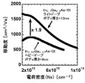
- FIG. 16 shows the relationship between the mobility of sample (1) and the charge density Ns. For comparison, FIG. 16 also shows data of a sample in which an InGaAs channel (thickness 9 nm) is heavily doped without forming a source and drain into an Ni—InGaAs alloy.
- the channel (1) has a low channel doping concentration of 1 ⁇ 10 16 atoms / cm 3 , a high on-current was observed. This seems to be due to the fact that the source and drain are made of Ni—InGaAs alloy. As shown in FIG.
- the Id-Vd characteristic of sample (1) is good.
- the mobility of the sample (1) was about 1.9 times that of the comparative example in which the source and drain were not made of Ni—InGaAs alloy. The effect of improving the mobility by the source / drain of the Ni—InGaAs alloy was confirmed.
- FIG. 17 shows the Id-Vg characteristic of sample (5). A three-digit on / off ratio and a low subthreshold coefficient of 183 mV / dec were observed.
- FIG. 18 shows the Id-Vg characteristic of sample (3). A very good characteristic of 7-digit on / off ratio and sub-threshold coefficient 103 mV / dec was observed.
- FIG. 19 shows the mobility of the sample (5) in relation to the charge density Ns. In FIG. 19, the value of sample (1) (without buffer) and the value of Si MOSFET are also shown for comparison. The mobility of sample (5) was 4.2 times higher than that of Si MOSFET and 1.6 times higher than that of sample (1). The effect of improving the mobility by the stacked channel of In 0.3 Ga 0.7 As / In 0.7 Ga 0.3 As / In 0.3 Ga 0.7 As was confirmed.
- FIG. 20 shows the channel layer thickness dependence of the mobility of samples (1) to (5).
- the mobility rapidly decreases from the vicinity of the thickness of the channel layer (total body thickness) being less than 10 nm, In 0.3 Ga 0.7 As / In 0.7 Ga 0.3 As / In 0.
- the 3 Ga 0.7 As stacked channel structure (with buffer) can maintain high mobility even with a thin channel thickness as compared with a single layer (without buffer). It was also found that the mobility in the stacked channel structure is higher than that in the bulk case.
- Example 2 In the same manner as in Example 1, an InGaAs layer was epitaxially grown on the InP substrate with the plane orientation (001) by the MOVPE method, and an Al 2 O 3 layer was formed on the InGaAs layer by the ALD method. Separately, an Al 2 O 3 layer was formed on the silicon substrate by ALD. The respective Al 2 O 3 layers of the InP substrate and the silicon substrate were subjected to a hydrophilic treatment, and the InP substrate and the silicon substrate were bonded together, and then InP was selectively removed with an HCl solution. Thus, a semiconductor substrate composed of InGaAs layer / Al 2 O 3 layer (BOX layer) / silicon substrate was produced.
- BOX layer Al 2 O 3 layer
- an Al 2 O 3 layer having a thickness of 10 nm is formed on the InGaAs layer by the ALD method. Formed.
- a gate electrode made of tantalum was formed by sputtering, and after post metallization annealing, a nickel film having a thickness of 20 nm was formed. The nickel film was subjected to RTA treatment at 250 ° C. to form a source / drain (S / D) of a Ni—InGaAs alloy, and a field effect transistor was produced.
- the gate length L of the field effect transistor was 5 ⁇ m and the gate width W was 100 ⁇ m.
- Samples (6) to (9) having the following four types of InGaAs layers were produced.
- (6) In 0.3 Ga 0.7 As / InAs / In 0.3 laminating the thickness of the Ga 0.7 As is 3/3 / 3nm (7)
- In 0.3 Ga 0.7 As / In 0.7 Ga 0.3 As / In 0.3 Ga 0.7 As each thickness is 3/5/3 nm (8) 10 nm thick In 0.7 Ga 0.3 As (single layer) (9) 20 nm thick In 0.53 Ga 0.47 As (single layer) 21 to 23 below
- the samples of (8) and (9) may be referred to as “no buffer” or “single channel”, and the samples of (6) and (7) may be referred to as “buffered”. May be called.
- the thickness of the InGaAs layer is sometimes referred to as “body thickness”.
- the thickness of In 0.7 Ga 0.3 As or In 0.53 Ga 0.47 As is used.
- channel thickness sometimes referred to as “channel thickness”.
- FIG. 21 is a cross-sectional TEM photograph of sample (6). Even when the channel layer was InAs, the structure of each layer was appropriately formed as in Example 1, and the overlap of the Ni—InGaAs alloy under the gate was also moderate. The source / drain of the Ni—InGaAs alloy was formed by self-alignment.
- FIG. 22 shows the Id-Vg characteristic of Sample (6). Even when the channel layer is InAs, an appropriate transistor operation was shown as in the first embodiment.
- FIG. 23 shows the relationship between the mobility at room temperature of samples (6) to (9) and the charge density Ns.
- the sample (6) in which the indium composition of the layer corresponding to the first crystal layer 108 is 1 has a higher mobility than the sample (7) in which the indium composition of the layer corresponding to the first crystal layer 108 is 0.7. was observed. It can be said that the higher the indium composition, the higher the mobility.
- the maximum mobility of the sample (6) reaches 3180 cm 2 / Vs, and the mobility is 3180 cm 2 for the first time in an ultra-thin body InAs laminated channel (ultrathin body (UTB) InAs-composite-OI channel) with a film thickness of 10 nm or less. / Vs was achieved.
- UTB ultra-thin body
- InAs-composite-OI channel ultra-thin body
- Example 3 In the same manner as in Example 1, an InGaAs layer was epitaxially grown on the InP substrate with the plane orientation (001) by the MOVPE method, and an Al 2 O 3 layer was formed on the InGaAs layer by the ALD method. Separately, an Al 2 O 3 layer was formed on the silicon substrate by ALD. The respective Al 2 O 3 layers of the InP substrate and the silicon substrate were subjected to a hydrophilic treatment, and the InP substrate and the silicon substrate were bonded together, and then InP was selectively removed with an HCl solution. Thus, a semiconductor substrate composed of InGaAs layer / Al 2 O 3 layer (BOX layer) / silicon substrate was produced.
- BOX layer Al 2 O 3 layer
- an Al 2 O 3 layer having a thickness of 10 nm is formed on the InGaAs layer by the ALD method. Formed.
- a gate electrode made of tantalum was formed by sputtering and electron beam lithography. The width of the gate electrode was set to about 200 nm, and microfabrication was attempted.
- post metallization annealing a 20 nm thick nickel film was formed. The nickel film was subjected to RTA treatment at 250 ° C. to form a source / drain (S / D) of a Ni—InGaAs alloy.
- the source / drain grew laterally (lateral direction) by the thermal reaction between the InGaAs layer and nickel, and the portions of the source and drain regions facing each other were formed under the gate electrode. Thus, a field effect transistor was produced.
- the gate length L of the field effect transistor was about 55 nm.
- Samples (10) and (11) having the following two types of InGaAs layers were prepared.
- the sample (11) may be referred to as “no buffer” or “single channel”, and the sample (10) may be referred to as “buffered”.
- the thickness of the InGaAs layer may be referred to as “body thickness”
- the thickness of In 0.53 Ga 0.47 As in the sample of (11) may be referred to as “channel thickness”.
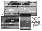
- FIG. 24 and 25 are cross-sectional TEM photographs of sample (10). Similar to the first embodiment, the structure of each layer is appropriately formed. Referring to FIG. 25, an Ni—InGaAs alloy overlap is formed under the gate of the InGaAs layer, and the overlap length from the gate end is about several tens of nm. If the width of the gate electrode is set to several hundred nm and the overlap length is controlled by the heat treatment temperature or time, the gate length (distance between the source and drain) of the transistor can be precisely and easily controlled. It can also be seen that the source / drain of the Ni—InGaAs alloy can be formed by self-alignment. By such a method, a planar MOSFET having a channel length of 100 nm or less can be easily manufactured.
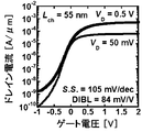
- FIG. 26 shows the Id-Vg characteristics of sample (10).
- FIG. 27 shows the Id-Vd characteristic of sample (10). It was found that even a MOSFET on an InAs laminated channel insulating layer whose gate length was miniaturized to 55 nm showed good transistor characteristics.
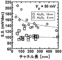
- FIG. 28 shows the channel length dependency of the SS value (subthreshold value) of sample (11), and FIG. 29 shows the channel length dependency of the DIBL value (barrier lowering effect value) of sample (11).
- the SS value is smaller when the thickness of Al 2 O 3 is 6 nm than when it is 12 nm. This is considered to be an effect that the channel is formed at a location closer to the gate electrode.
- the DIBL value is smaller when the thickness of Al 2 O 3 is 6 nm than when it is 12 nm. It can be seen that the transistor performance is improved by the effect of reducing (scaling) the thickness of the effective oxide film thickness (EOT).
- FIG. 30 to 35 show the channel length dependency of the threshold value (Vth) (FIG. 30), the channel length dependency of the SS value (FIG. 31), and the DIBL value of the sample (10) and the sample (11), respectively.
- Channel length dependency (FIG. 32), on-current / off-current characteristics (FIG. 33), DIBL dependency of on-current (FIG. 34), and channel length dependency of total resistance value between source and drain (FIG. 35) .
- the threshold value was defined by the gate voltage at a drain current of 10 ⁇ 6 ⁇ A / ⁇ m, and DIBL was evaluated by the difference in threshold value at each drain voltage.
- FIG. 31 shows that neither the sample (10) nor the sample (11) has a rapid change in threshold value (roll-off) or a phenomenon in which the threshold value shifts to a negative bias. Since the phenomenon such as roll-off occurs due to the short channel effect, it was confirmed that the short channel effect was suppressed.
- the effect of suppressing the short channel effect is considered to be obtained by an OI structure in which a transistor is formed on an insulating layer (BOX layer), and the superiority of the OI structure was confirmed.
- the sample (10) can achieve about four times the on-current (when the off-current is 1 nA / ⁇ m) as compared with the sample (11). From FIG. 35, the sample (10) Compared with the sample (11), it was found that about four times the on-current (in the case of the same DIBL value) can be realized.
- the parasitic resistance between the source and the drain of the sample (10) is 1.16 k ⁇ ⁇ ⁇ m
- the parasitic resistance between the source and the drain of the sample (11) is 5.54 k ⁇ ⁇ ⁇ m.
- the parasitic resistance between the source and the drain corresponds to the total resistance value R tot between the source and the drain when the channel length Lch is zero. That is, it can be seen that the parasitic resistance of the sample (10) is about one-fifth compared to the parasitic resistance of the sample (11).
- FIG. 36 shows the channel length dependence of the SS value of the field effect transistor in Sample (10), Sample (11), and Reference Examples 1, 2, and 4.
- FIG. 37 shows Sample (10) and Reference Examples 1 to 4 The channel length dependence of the DIBL value of the field effect transistor at is shown. Table 1 compares the main structure and characteristics of the sample (10) which is Example 3 and the reference examples 1 to 4.
- Reference Examples 1 to 4 are transistors described in the following documents, all of which have a trigate type, fin type, or gate all-around type three-dimensional gate structure.
- Reference example 1 M. Radosavljevic et al., 2010 IEDM, pp. 126-129.
- Reference example 2 M. Radosavljevic et al., 2011 IEDM, pp. 765-768.
- Reference Example 3 H. C. Chin et al., EDL 32, 2 (2011).
- Reference example 4 J. J. Gu et al., 2011 IEDM, pp. 769-772.
- the sample (10) is a MOSFET having a planar gate structure, but has a characteristic equivalent to or exceeding that of a three-dimensional gate.
- first element such as a layer, a region or a substrate
- first element is located directly on the second element.
- first element is indirectly positioned on the second element with other elements interposed between the first element and the second element.
- the semiconductor layer 106 exposed through the opening refers to the semiconductor layer 106 at the bottom of the opening.
- the field effect transistor is an n-channel field effect transistor, the relationship of each electron affinity described in this specification may be reversed.
Landscapes
- Thin Film Transistor (AREA)
- Chemical & Material Sciences (AREA)
- Engineering & Computer Science (AREA)
- Materials Engineering (AREA)
- Formation Of Insulating Films (AREA)
- Junction Field-Effect Transistors (AREA)
Abstract
Description
非特許文献1 Ren, F. et al. Demonstration of enhancement-mode p- and n-channel GaAs MOSFETs with Ga2O3(Gd2O3) As gate oxide. Solid State Electron. 41, 1751-1753 (1997).
非特許文献2 Chin, H. C. et al. Silane-ammonia surface passivation for gallium arsenide surface-channel n-MOSFETs. IEEE Electron Device Lett. 30, 110-112 (2009).
非特許文献3 S.Arabasz,et al.著,Vac.80巻(2006年)、888ページ
(数1)
(ε1・d0)/(ε0・d1)>(V―δ)/δ
ただし、d0およびε0はゲート電極212と第1結晶層108とに挟まれたゲート下領域における第2絶縁体層210の厚さおよび比誘電率を示し、d1およびε1はゲート下領域における第2結晶層110の厚さおよび比誘電率を示す。δは、第2結晶層110と第1結晶層108との電子親和力の差であり、δ=Ea1-Ea2である。Vは、V=Vg-Vtで定義された電圧であり、Vgは電界効果トランジスタ200のゲート電極212に印加する電圧であり、Vtは閾値電圧である。電圧Vは、閾値電圧以上の電圧をゲート電極212にかけて電界効果トランジスタ200を動作させた場合に、ゲート下領域の第2結晶層110と第2絶縁体層210の積層構造の部分に印加される電圧として近似できる。
(数2)
ΔV=V×(d1/ε1)/((d1/ε1)+d0/ε0)
ここでΔV<δであれば多くのチャネル電子を第2絶縁体層210と第2結晶層110との間に誘起することができる。よって数3が得られる。
(数3)
V×(d1/ε1)/((d1/ε1)+d0/ε0)<δ
数3を整理することで数1が得られる。すなわち、数1の関係が満たされる場合に、第1結晶層108と第2結晶層110の界面に高移動度チャネル電子を誘起することができる。
面方位(001)のInP基板上に、MOVPE(Metal Organic Vapor Phase Epitaxy)法によりInGaAs層をエピタキシャル成長し、InGaAs層上にALD法によりAl2O3層を形成した。別途シリコン基板上にALD法によりAl2O3層を形成した。InP基板とシリコン基板のそれぞれのAl2O3層を親水化処理し、InP基板とシリコン基板とを貼り合わせた後、HCl溶液によりInPを選択的に除去した。これによりInGaAs層/Al2O3層(BOX層)/シリコン基板からなる半導体基板を作製した。
(1)10nm厚さのIn0.7Ga0.3As(単層)
(2)5nm厚さのIn0.7Ga0.3As(単層)
(3)In0.3Ga0.7As/In0.7Ga0.3As/In0.3Ga0.7Asの各厚さが2/1/3nmである積層
(4)In0.3Ga0.7As/In0.7Ga0.3As/In0.3Ga0.7Asの各厚さが2/3/3nmである積層
(5)In0.3Ga0.7As/In0.7Ga0.3As/In0.3Ga0.7Asの各厚さが2/5/3nmである積層
なお、以下の図13~図20において、(1)~(2)のサンプルを「バッファなし」または「単チャネル」と称する場合があり、(3)~(5)のサンプルを「バッファあり」と称する場合がある。InGaAs層の厚さを「ボディ厚さ」と称する場合があり、(3)~(5)のサンプルにおいてIn0.7Ga0.3Asの厚さを「チャネルの厚さ」と称する場合がある。
実施例1と同様に、面方位(001)のInP基板上に、MOVPE法によりInGaAs層をエピタキシャル成長し、InGaAs層上にALD法によりAl2O3層を形成した。別途シリコン基板上にALD法によりAl2O3層を形成した。InP基板とシリコン基板のそれぞれのAl2O3層を親水化処理し、InP基板とシリコン基板とを貼り合わせた後、HCl溶液によりInPを選択的に除去した。これによりInGaAs層/Al2O3層(BOX層)/シリコン基板からなる半導体基板を作製した。
(6)In0.3Ga0.7As/InAs/In0.3Ga0.7Asの各厚さが3/3/3nmである積層
(7)In0.3Ga0.7As/In0.7Ga0.3As/In0.3Ga0.7Asの各厚さが3/5/3nmである積層
(8)10nm厚さのIn0.7Ga0.3As(単層)
(9)20nm厚さのIn0.53Ga0.47As(単層)
なお、以下の図21~図23において、(8)、(9)のサンプルを「バッファなし」または「単チャネル」と称する場合があり、(6)、(7)のサンプルを「バッファあり」と称する場合がある。InGaAs層の厚さを「ボディ厚さ」と称する場合があり、(8)、(9)のサンプルにおいてIn0.7Ga0.3AsまたはIn0.53Ga0.47Asの厚さを「チャネルの厚さ」と称する場合がある。
実施例1と同様に、面方位(001)のInP基板上に、MOVPE法によりInGaAs層をエピタキシャル成長し、InGaAs層上にALD法によりAl2O3層を形成した。別途シリコン基板上にALD法によりAl2O3層を形成した。InP基板とシリコン基板のそれぞれのAl2O3層を親水化処理し、InP基板とシリコン基板とを貼り合わせた後、HCl溶液によりInPを選択的に除去した。これによりInGaAs層/Al2O3層(BOX層)/シリコン基板からなる半導体基板を作製した。
(10)In0.3Ga0.7As/InAs/In0.3Ga0.7Asの各厚さが3/3/3nmである積層
(11)10nm厚さのIn0.53Ga0.47As(単層)
なお、以下の図24~図37において、(11)のサンプルを「バッファなし」または「単チャネル」と称する場合があり、(10)のサンプルを「バッファあり」と称する場合がある。InGaAs層の厚さを「ボディ厚さ」と称する場合があり、(11)のサンプルにおいてIn0.53Ga0.47Asの厚さを「チャネルの厚さ」と称する場合がある。

参照例1:M. Radosavljevic et al., 2010 IEDM, pp. 126-129.
参照例2:M. Radosavljevic et al., 2011 IEDM, pp. 765-768.
参照例3:H. C. Chin et al., EDL 32, 2 (2011).
参照例4:J. J. Gu et al., 2011 IEDM, pp. 769-772.
Claims (14)
- ベース基板と第1絶縁体層と半導体層とを有し、
前記ベース基板、前記第1絶縁体層および前記半導体層が、前記ベース基板、前記第1絶縁体層、前記半導体層の順に位置し、
前記第1絶縁体層が、アモルファス状金属酸化物またはアモルファス状金属窒化物からなり、
前記半導体層が、第1結晶層および第2結晶層を含み、
前記第1結晶層および前記第2結晶層が、前記ベース基板の側から、前記第1結晶層、前記第2結晶層の順に位置し、
前記第1結晶層の電子親和力Ea1が、前記第2結晶層の電子親和力Ea2より大きい
半導体基板。 - 前記半導体層が、第3結晶層をさらに含み、
前記第1結晶層、前記第2結晶層および前記第3結晶層が、前記ベース基板の側から、前記第3結晶層、前記第1結晶層、前記第2結晶層の順に位置し、
前記第3結晶層の電子親和力Ea3が、前記第1結晶層の電子親和力Ea1より小さい
請求項1に記載の半導体基板。 - 前記第1結晶層がInx1Ga1-x1As(0<x1≦1)からなり、
前記第2結晶層がInx2Ga1-x2As(0≦x2<1)からなり、前記第3結晶層がInx3Ga1-x3As(0≦x3<1)からなり、
x1>x2、かつ、x1>x3の関係を満足する
請求項2に記載の半導体基板。 - 前記半導体層の厚さが、20nm以下である
請求項1に記載の半導体基板。 - 請求項1に記載の半導体基板を有する電界効果トランジスタであって、前記半導体層に電気的に接続されたソース電極およびドレイン電極を備える電界効果トランジスタ。
- 前記半導体層が、前記ソース電極と接触するソース領域または前記ドレイン電極と接触するドレイン領域を有し、
前記ソース領域または前記ドレイン領域が、前記半導体層を構成するIII族原子およびV族原子からなる群から選ばれた少なくとも1種の原子と金属原子との合金を含む
請求項5に記載の電界効果トランジスタ。 - 前記金属原子がニッケル原子である
請求項6に記載の電界効果トランジスタ。 - 前記半導体層の前記ベース基板とは反対の側にゲート電極を有し、
前記ソース領域の前記ドレイン領域側に位置する界面および前記ドレイン領域の前記ソース領域側に位置する界面が、前記ゲート電極と前記ベース基板に挟まれた前記半導体層の領域であるゲート電極下領域に形成されている
請求項6に記載の電界効果トランジスタ。 - 前記電界効果トランジスタがnチャネル型電界効果トランジスタであり、
前記ソース領域または前記ドレイン領域は、ドナー不純物原子をさらに含む
請求項6に記載の電界効果トランジスタ。 - 前記電界効果トランジスタがpチャネル型電界効果トランジスタであり、
前記ソース領域または前記ドレイン領域は、アクセプタ不純物原子をさらに含む
請求項6に記載の電界効果トランジスタ。 - 半導体層形成基板上に半導体層をエピタキシャル結晶成長法により形成する半導体層形成ステップと、
前記半導体層上に第1絶縁体層を原子層堆積法により成膜する第1絶縁体層形成ステップと、
前記第1絶縁体層上にベース基板を接合する接合ステップと、
前記半導体層形成基板を除去する除去ステップと、を備え、
前記半導体層形成ステップが、前記半導体層形成基板上に第2結晶層をエピタキシャル結晶成長法により形成する第1ステップと、前記第1ステップの後に、前記第2結晶層の電子親和力Ea2より大きい電子親和力Ea1を有する第1結晶層を、前記第2結晶層上にエピタキシャル結晶成長法により形成する第2ステップと、を有する
半導体基板の製造方法。 - 前記半導体層形成ステップが、前記第2ステップの後に、前記第1結晶層の電子親和力Ea1より小さい電子親和力Ea3を有する第3結晶層を、前記第1結晶層上にエピタキシャル結晶成長法により形成する第3ステップをさらに有する
請求項11に記載の半導体基板の製造方法。 - 請求項11に記載の半導体基板の製造方法により製造された前記半導体基板の前記半導体層上に、原子層堆積法により第2絶縁体層を成膜するステップと、
前記第2絶縁体層上にゲート電極を形成するステップと、
前記ゲート電極が形成された領域以外の前記第2絶縁体層の一部をエッチングして、前記半導体層に達する開口を形成するステップと、
前記開口により露出する前記半導体層に接する金属膜を形成するステップと、
前記金属膜を熱処理して、前記金属膜と接する前記半導体層の部分にソース領域またはドレイン領域の少なくとも一方を形成するステップと、
を備えた電界効果トランジスタの製造方法。 - 前記ソース領域または前記ドレイン領域の少なくとも一方を形成するステップにおいて、前記熱処理の温度および時間から選択された1以上の条件を制御して、前記ソース領域の前記ドレイン領域側に位置する界面および前記ドレイン領域の前記ソース領域側に位置する界面から選択された1以上の界面の位置を、前記ゲート電極と前記ベース基板に挟まれた前記半導体層の領域であるゲート電極下領域に形成するよう制御する
請求項13に記載の電界効果トランジスタの製造方法。
Priority Applications (3)
| Application Number | Priority Date | Filing Date | Title |
|---|---|---|---|
| CN201280009842.2A CN103384917B (zh) | 2011-03-02 | 2012-03-02 | 半导体基板及其制造方法 |
| KR1020137024098A KR20140027938A (ko) | 2011-03-02 | 2012-03-02 | 반도체 기판, 전계 효과 트랜지스터, 반도체 기판의 제조 방법, 및 전계 효과 트랜지스터의 제조 방법 |
| US14/015,775 US8901656B2 (en) | 2011-03-02 | 2013-08-30 | Semiconductor wafer, field-effect transistor, method of producing semiconductor wafer, and method of producing field-effect transistor |
Applications Claiming Priority (2)
| Application Number | Priority Date | Filing Date | Title |
|---|---|---|---|
| JP2011045510 | 2011-03-02 | ||
| JP2011-045510 | 2011-03-02 |
Related Child Applications (1)
| Application Number | Title | Priority Date | Filing Date |
|---|---|---|---|
| US14/015,775 Continuation-In-Part US8901656B2 (en) | 2011-03-02 | 2013-08-30 | Semiconductor wafer, field-effect transistor, method of producing semiconductor wafer, and method of producing field-effect transistor |
Publications (1)
| Publication Number | Publication Date |
|---|---|
| WO2012117745A1 true WO2012117745A1 (ja) | 2012-09-07 |
Family
ID=46757687
Family Applications (1)
| Application Number | Title | Priority Date | Filing Date |
|---|---|---|---|
| PCT/JP2012/001477 Ceased WO2012117745A1 (ja) | 2011-03-02 | 2012-03-02 | 半導体基板及びその製造方法 |
Country Status (6)
| Country | Link |
|---|---|
| US (1) | US8901656B2 (ja) |
| JP (1) | JP2012195579A (ja) |
| KR (1) | KR20140027938A (ja) |
| CN (1) | CN103384917B (ja) |
| TW (1) | TWI528548B (ja) |
| WO (1) | WO2012117745A1 (ja) |
Cited By (1)
| Publication number | Priority date | Publication date | Assignee | Title |
|---|---|---|---|---|
| CN105900243A (zh) * | 2013-09-27 | 2016-08-24 | 英特尔公司 | 在包覆的iii-v族沟道材料中实现高迁移率的方法 |
Families Citing this family (7)
| Publication number | Priority date | Publication date | Assignee | Title |
|---|---|---|---|---|
| CN102560634A (zh) * | 2012-02-20 | 2012-07-11 | 华南理工大学 | 在GaAs衬底上生长InGaAs薄膜的方法 |
| US9389199B2 (en) * | 2013-03-14 | 2016-07-12 | Taiwan Semiconductor Manufacturing Company, Ltd. | Backside sensing bioFET with enhanced performance |
| US8941123B2 (en) * | 2013-05-30 | 2015-01-27 | International Business Machines Corporation | Local interconnects by metal-III-V alloy wiring in semi-insulating III-V substrates |
| KR102366953B1 (ko) | 2016-01-06 | 2022-02-23 | 삼성전자주식회사 | 반도체 장치 및 이의 제조 방법 |
| TWI611587B (zh) * | 2016-08-31 | 2018-01-11 | 明新科技大學 | 氧化物薄膜電晶體 |
| CN111081771B (zh) * | 2019-12-24 | 2023-04-18 | 成都挚信电子技术有限责任公司 | 一种绝缘层掩埋型晶体管结构及器件 |
| JP7859491B2 (ja) * | 2022-05-16 | 2026-05-15 | Ntt株式会社 | 半導体積層構造およびその作製方法、ならびに半導体装置の製造方法 |
Citations (7)
| Publication number | Priority date | Publication date | Assignee | Title |
|---|---|---|---|---|
| JPH05327127A (ja) * | 1992-05-15 | 1993-12-10 | Fujitsu Ltd | 半導体装置及びその製造方法 |
| JP2006012986A (ja) * | 2004-06-23 | 2006-01-12 | Canon Inc | 半導体層の製造方法及び基板の製造方法 |
| JP2007096126A (ja) * | 2005-09-29 | 2007-04-12 | Sharp Corp | トランジスタおよび電子デバイス |
| JP2009238955A (ja) * | 2008-03-26 | 2009-10-15 | Univ Of Tokyo | 半導体基板、半導体装置、および半導体装置の製造方法 |
| JP2010010663A (ja) * | 2008-05-13 | 2010-01-14 | Imec | 小型化可能な量子井戸デバイスおよびその製造方法 |
| JP2010232568A (ja) * | 2009-03-29 | 2010-10-14 | Univ Of Tokyo | 半導体デバイス及びその製造方法 |
| JP2011009722A (ja) * | 2009-05-26 | 2011-01-13 | Sumitomo Chemical Co Ltd | 半導体基板、半導体基板の製造方法、および電子デバイス |
Family Cites Families (12)
| Publication number | Priority date | Publication date | Assignee | Title |
|---|---|---|---|---|
| JPH05102196A (ja) * | 1991-10-03 | 1993-04-23 | Rohm Co Ltd | 電界効果トランジスタ |
| JPH11354776A (ja) * | 1998-06-10 | 1999-12-24 | Hitachi Ltd | 半導体結晶積層体およびそれを用いた半導体装置 |
| US6963090B2 (en) | 2003-01-09 | 2005-11-08 | Freescale Semiconductor, Inc. | Enhancement mode metal-oxide-semiconductor field effect transistor |
| US6998657B2 (en) * | 2003-10-21 | 2006-02-14 | Micron Technology, Inc. | Single poly CMOS imager |
| US7282425B2 (en) * | 2005-01-31 | 2007-10-16 | International Business Machines Corporation | Structure and method of integrating compound and elemental semiconductors for high-performance CMOS |
| US7799669B2 (en) * | 2007-04-27 | 2010-09-21 | Texas Instruments Incorporated | Method of forming a high-k gate dielectric layer |
| US20080251814A1 (en) * | 2007-04-16 | 2008-10-16 | International Business Machines Corporation | Hetero-bonded semiconductor-on-insulator substrate with an unpinning dielectric layer |
| US20090267130A1 (en) * | 2008-04-28 | 2009-10-29 | International Business Machines Corporation | Structure and process integration for flash storage element and dual conductor complementary mosfets |
| WO2010067525A1 (ja) * | 2008-12-08 | 2010-06-17 | 住友化学株式会社 | 半導体装置、半導体装置の製造方法、半導体基板、および半導体基板の製造方法 |
| US20100148153A1 (en) * | 2008-12-16 | 2010-06-17 | Hudait Mantu K | Group III-V devices with delta-doped layer under channel region |
| US8455860B2 (en) * | 2009-04-30 | 2013-06-04 | Taiwan Semiconductor Manufacturing Company, Ltd. | Reducing source/drain resistance of III-V based transistors |
| CN102460642A (zh) * | 2009-06-24 | 2012-05-16 | 株式会社半导体能源研究所 | 半导体衬底的再加工方法及soi衬底的制造方法 |
-
2012
- 2012-02-28 JP JP2012042589A patent/JP2012195579A/ja active Pending
- 2012-03-02 WO PCT/JP2012/001477 patent/WO2012117745A1/ja not_active Ceased
- 2012-03-02 CN CN201280009842.2A patent/CN103384917B/zh not_active Expired - Fee Related
- 2012-03-02 KR KR1020137024098A patent/KR20140027938A/ko not_active Withdrawn
- 2012-03-02 TW TW101106933A patent/TWI528548B/zh active
-
2013
- 2013-08-30 US US14/015,775 patent/US8901656B2/en not_active Expired - Fee Related
Patent Citations (7)
| Publication number | Priority date | Publication date | Assignee | Title |
|---|---|---|---|---|
| JPH05327127A (ja) * | 1992-05-15 | 1993-12-10 | Fujitsu Ltd | 半導体装置及びその製造方法 |
| JP2006012986A (ja) * | 2004-06-23 | 2006-01-12 | Canon Inc | 半導体層の製造方法及び基板の製造方法 |
| JP2007096126A (ja) * | 2005-09-29 | 2007-04-12 | Sharp Corp | トランジスタおよび電子デバイス |
| JP2009238955A (ja) * | 2008-03-26 | 2009-10-15 | Univ Of Tokyo | 半導体基板、半導体装置、および半導体装置の製造方法 |
| JP2010010663A (ja) * | 2008-05-13 | 2010-01-14 | Imec | 小型化可能な量子井戸デバイスおよびその製造方法 |
| JP2010232568A (ja) * | 2009-03-29 | 2010-10-14 | Univ Of Tokyo | 半導体デバイス及びその製造方法 |
| JP2011009722A (ja) * | 2009-05-26 | 2011-01-13 | Sumitomo Chemical Co Ltd | 半導体基板、半導体基板の製造方法、および電子デバイス |
Non-Patent Citations (1)
| Title |
|---|
| L. CZORNOMAZ ET AL.: "Self-aligned S/D regions for InGaAs MOSFETs", SOLID-STATE DEVICE RESEARCH CONFERENCE (ESSDERC), 2011 PROCEEDINGS OF THE EUROPEAN, 12 September 2011 (2011-09-12), pages 219 - 222 * |
Cited By (2)
| Publication number | Priority date | Publication date | Assignee | Title |
|---|---|---|---|---|
| CN105900243A (zh) * | 2013-09-27 | 2016-08-24 | 英特尔公司 | 在包覆的iii-v族沟道材料中实现高迁移率的方法 |
| EP3050114A4 (en) * | 2013-09-27 | 2017-05-03 | Intel Corporation | Methods to achieve high mobility in cladded iii-v channel materials |
Also Published As
| Publication number | Publication date |
|---|---|
| US20130341721A1 (en) | 2013-12-26 |
| JP2012195579A (ja) | 2012-10-11 |
| KR20140027938A (ko) | 2014-03-07 |
| TWI528548B (zh) | 2016-04-01 |
| CN103384917A (zh) | 2013-11-06 |
| US8901656B2 (en) | 2014-12-02 |
| TW201244080A (en) | 2012-11-01 |
| CN103384917B (zh) | 2016-03-09 |
Similar Documents
| Publication | Publication Date | Title |
|---|---|---|
| US8901656B2 (en) | Semiconductor wafer, field-effect transistor, method of producing semiconductor wafer, and method of producing field-effect transistor | |
| US8106381B2 (en) | Semiconductor structures with rare-earths | |
| US8653599B1 (en) | Strained SiGe nanowire having (111)-oriented sidewalls | |
| CN104900693B (zh) | 非平面锗量子阱装置 | |
| KR102879149B1 (ko) | 탄소-도핑된 이형 층들을 갖는 모놀리식 상보형 전계 효과 트랜지스터들 | |
| CN107731902B (zh) | 第iii族氮化物常关晶体管的层结构 | |
| Yeo et al. | Germanium-based transistors for future high performance and low power logic applications | |
| US9905421B2 (en) | Improving channel strain and controlling lateral epitaxial growth of the source and drain in FinFET devices | |
| US12100755B2 (en) | Channel structures including doped 2D materials for semiconductor devices | |
| WO2012169213A1 (ja) | 半導体デバイス、半導体基板、半導体基板の製造方法および半導体デバイスの製造方法 | |
| Convertino et al. | InGaAs FinFETs 3-D sequentially integrated on FDSOI Si CMOS with record performance | |
| Tian et al. | A novel nanoscaled device concept: Quasi-SOI MOSFET to eliminate the potential weaknesses of UTB SOI MOSFET | |
| Huang et al. | Highly stacked GeSn nanosheets by CVD epitaxy and highly selective isotropic dry etching | |
| CN104425269B (zh) | 鳍式场效应晶体管及其形成方法 | |
| Barraud et al. | Strained silicon directly on insulator N-and P-FET nanowire transistors | |
| Liu et al. | Vertical heterojunction Ge0. 92Sn0. 08/Ge gate-all-around nanowire pMOSFETs with NiGeSn contact | |
| CN100380589C (zh) | 具有应力吸收半导体层的半导体组件及其制造方法 | |
| Goh et al. | Gate-all-around CMOS (InAs n-FET and GaSb p-FET) based on vertically-stacked nanowires on a Si platform, enabled by extremely-thin buffer layer technology and common gate stack and contact modules | |
| WO2012169208A1 (ja) | 半導体基板の製造方法および半導体基板 | |
| Verma et al. | Performance evaluation of InN-based Junctionless FETs under single and double gate architectures | |
| Liu et al. | V T Tuning of Split-Gate GeSi Nanosheet CFETs With Dual Work Function Metals | |
| JP7444285B2 (ja) | 半導体構造および電界効果トランジスタの作製方法 | |
| Liu et al. | III-V Materials and Devices | |
| CN121985724A (zh) | 半导体结构的制作方法 | |
| CN106611793A (zh) | 应变堆叠的纳米片fet和/或量子阱堆叠的纳米片 |
Legal Events
| Date | Code | Title | Description |
|---|---|---|---|
| WWE | Wipo information: entry into national phase |
Ref document number: 201280009842.2 Country of ref document: CN |
|
| 121 | Ep: the epo has been informed by wipo that ep was designated in this application |
Ref document number: 12752861 Country of ref document: EP Kind code of ref document: A1 |
|
| NENP | Non-entry into the national phase |
Ref country code: DE |
|
| ENP | Entry into the national phase |
Ref document number: 20137024098 Country of ref document: KR Kind code of ref document: A |
|
| 122 | Ep: pct application non-entry in european phase |
Ref document number: 12752861 Country of ref document: EP Kind code of ref document: A1 |