WO2012117530A1 - 信号遅延装置、信号遅延装置の制御方法 - Google Patents
信号遅延装置、信号遅延装置の制御方法 Download PDFInfo
- Publication number
- WO2012117530A1 WO2012117530A1 PCT/JP2011/054655 JP2011054655W WO2012117530A1 WO 2012117530 A1 WO2012117530 A1 WO 2012117530A1 JP 2011054655 W JP2011054655 W JP 2011054655W WO 2012117530 A1 WO2012117530 A1 WO 2012117530A1
- Authority
- WO
- WIPO (PCT)
- Prior art keywords
- delay
- signal
- output
- input
- selection
- Prior art date
- Legal status (The legal status is an assumption and is not a legal conclusion. Google has not performed a legal analysis and makes no representation as to the accuracy of the status listed.)
- Ceased
Links
Images









Classifications
-
- H—ELECTRICITY
- H03—ELECTRONIC CIRCUITRY
- H03K—PULSE TECHNIQUE
- H03K5/00—Manipulating of pulses not covered by one of the other main groups of this subclass
- H03K5/13—Arrangements having a single output and transforming input signals into pulses delivered at desired time intervals
-
- H—ELECTRICITY
- H03—ELECTRONIC CIRCUITRY
- H03K—PULSE TECHNIQUE
- H03K5/00—Manipulating of pulses not covered by one of the other main groups of this subclass
- H03K5/13—Arrangements having a single output and transforming input signals into pulses delivered at desired time intervals
- H03K5/14—Arrangements having a single output and transforming input signals into pulses delivered at desired time intervals by the use of delay lines
-
- H—ELECTRICITY
- H03—ELECTRONIC CIRCUITRY
- H03K—PULSE TECHNIQUE
- H03K19/00—Logic circuits, i.e. having at least two inputs acting on one output; Inverting circuits
- H03K19/0008—Arrangements for reducing power consumption
- H03K19/0016—Arrangements for reducing power consumption by using a control or a clock signal, e.g. in order to apply power supply
-
- H—ELECTRICITY
- H03—ELECTRONIC CIRCUITRY
- H03K—PULSE TECHNIQUE
- H03K5/00—Manipulating of pulses not covered by one of the other main groups of this subclass
- H03K5/13—Arrangements having a single output and transforming input signals into pulses delivered at desired time intervals
- H03K5/133—Arrangements having a single output and transforming input signals into pulses delivered at desired time intervals using a chain of active delay devices
Definitions
- the present invention relates to a signal delay device and a signal delay device control method.
- a signal delay device that delays and outputs an input signal such as a clock signal of a semiconductor circuit device such as an LSI (Large Scale Integrated Circuit).
- input signals are input to multiple delay units with different delay times, one of the delay units is set to the operating state according to the switching control signal, and the signal delayed by the delay unit set to the operating state is output. There was a signal delay device to do.
- the conventional signal delay device requires processing such as calculation of delay amount or weighting of delay amount in order to set the delay amount given to the input signal.
- an object of the present invention is to provide a signal delay device that can easily set a delay amount given to an input signal and a control method of the signal delay device.
- a signal delay device is a signal delay device that outputs a delay signal obtained by delaying an input signal.
- the signal delay device includes a plurality of delay units connected in series to each other, and a signal input by each delay unit.
- a selection means for outputting the delay signal which is inputted with an output of the selection unit of the previous stage and outputs either an output from the delay unit or an output of the selection unit of the previous stage according to the selection signal to be inputted; and the signal delay device
- a register unit that holds delay setting data for setting a delay amount of the signal, and a selection unit that selects a corresponding delay unit output based on the delay setting data held by the register unit Generates No. characterized by having a selection signal generator outputting to said selection means.
- FIG. 1 is a diagram illustrating an information processing device including a signal delay device according to Embodiment 1.
- FIG. 1 is a diagram illustrating a signal delay device according to a first embodiment.
- 3 is a diagram illustrating a circuit configuration of a delay adjustment determination unit 140 of the signal delay device according to Embodiment 1.
- FIG. 1 is a diagram illustrating an information processing device including a signal delay device according to Embodiment 1.
- FIG. 1 is a diagram illustrating a signal delay device according to a first embodiment.
- 3 is a diagram illustrating a circuit configuration of a delay adjustment determination unit 140 of the signal delay device according to Embodiment 1.
- FIG. 3 is a timing chart illustrating an operation of a delay adjustment determination unit 140 of the signal delay device according to the first embodiment.
- 3 is a diagram illustrating a circuit configuration of a delay setting data generation unit 150 of the signal delay device according to Embodiment 1.
- FIG. 3 is a diagram illustrating a delay adjustment circuit 110A for fine adjustment, a selection signal generation unit 120, a shift register 130, and a change flag FF170 of the signal delay device 100 according to the first embodiment.
- FIG. 3 is a diagram illustrating an example of a circuit configuration of a part of a selection signal generation unit 120.
- FIG. 6 is a diagram illustrating an example of delay setting data held by the shift register 130 of the signal delay device 100 according to the first embodiment.
- FIG. 6 is a diagram illustrating delay setting data held by the shift register 130 of the signal delay device 100 according to the first embodiment together with a change flag and a selection signal.
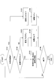
- FIG. 4 is a flowchart showing a delay process in the signal delay device 100 according to the first embodiment.
- 3 is a timing chart showing a relationship between delay setting data and a selection signal in a fine adjustment delay adjustment circuit 110A of the signal delay device 100 according to the first embodiment.
- FIG. 6 is a diagram illustrating a signal delay device according to a second embodiment.
- FIG. 10 is a diagram illustrating circuit configurations of a delay adjustment circuit 110A, a selection signal generation unit 220, and a shift register 230 of the signal delay device 200 according to the second embodiment.
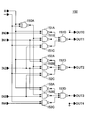
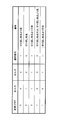
- FIG. 7 is a table showing a combination of delay setting data for obtaining selection signals 1 to 4 and an output of a NAND circuit 251 output as selection signals 1 to 4 in the signal delay device 200 of the second embodiment. It is a figure which shows typically switching of the return point of the signal in the delay adjustment circuit 110A of the signal delay apparatus 200 of Embodiment 2.
- FIG. 10 is a timing chart showing a relationship between delay setting data and a selection signal in a delay adjustment circuit 110A for fine adjustment of the signal delay device 200 according to the second embodiment.
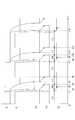
- FIGS. 1A and 1B are diagrams showing a delay adjustment circuit of a signal delay device of a comparative example.
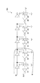
- the delay adjustment circuit 10 of the comparative signal delay device shown in FIG. 1A includes inverters 11, 12, 13, 14, 15, selectors 21, 22, 23, 24, 25, and inverters 31, 32, 33, 34, 35. including.
- the inverters 11 to 15, the selectors 21 to 25, and the inverters 31 to 35 are delay elements.
- the inverters 11 to 15 are inverters on the forward side for propagating signals to the selectors 21 to 25 that are signal folding points.
- the inverters 31 to 35 are propagated after the signals are folded by the selectors 21 to 25. This is a return side inverter.
- Each of the inverters 11 to 15 is a negation circuit that inverts and outputs an input signal.
- the inverters 11 to 15 are connected in series by connecting the output terminal and the input terminal, respectively.
- the input terminal of the inverter 11 is connected to the input terminal IN of the delay adjustment circuit 10, and the output terminal of the inverter 15 is connected to one input terminal of the selector 25.
- the selectors 21 to 25 are provided corresponding to the inverters 11 to 15, respectively.
- the selectors 21 to 25 have two input terminals, and select and output one of the inputs according to the level (“1” or “0”) of the selection signal.
- the inverters 31 to 35 are negation circuits that invert input signals and output them, and are provided corresponding to the selectors 21 to 25, respectively.
- the inverters 31 to 35 are alternately connected in series with the selectors 21 to 25, and invert the outputs of the selectors 21 to 25, respectively.
- the output terminal of the inverter 15 is connected to one input terminal of the selector 25.
- Data X is input to the other input terminal of the selector 25. Note that the data X is fixed data of “0” or “1”.
- the output terminal of the inverter 14 is connected to one input terminal of the selector 24, and the output terminal of the inverter 35 is connected to the other input terminal.
- the output terminal of the inverter 13 is connected to one input terminal of the selector 23, and the output terminal of the inverter 34 is connected to the other input terminal.
- the output terminal of the inverter 12 is connected to one input terminal of the selector 22, and the output terminal of the inverter 33 is connected to the other input terminal.
- the output terminal of the inverter 11 is connected to one input terminal of the selector 21, and the output terminal of the inverter 32 is connected to the other input terminal.
- the output terminal of the selector 21 is connected to the input terminal of the inverter 31, and the output terminal of the inverter 31 is connected to the output terminal OUT of the delay adjustment circuit 10.
- the delay adjustment circuit 10 adjusts the amount of delay of the signal input to the input terminal IN and outputs it from the output terminal OUT depending on where in the selectors 21 to 25 the signal input to the input terminal IN is folded. .
- the delay adjustment circuit 10 adjusts the delay amount by selecting the number of inverters through which the signal input to the input terminal IN passes using the selectors 21 to 25.
- the position at which the signal input from the input terminal IN returns is determined by a selector (any one of 21 to 25) in which the selection signal is first set to “0” when viewed from the input terminal IN side.
- the selection signal input to each of the selectors 21 to 25 is set to “1”, “0”, “0”, “0”, “0”. If so, the selector 22 selects the output of the inverter 12. For this reason, a signal input to the input terminal IN is propagated from the inverter 11 to the inverter 12, input from the output terminal of the inverter 12 to the selector 22, and folded by the selector 22.
- the inverters 13, 14, 15, the selectors 23, 24, 25, and the inverters 33, 34, 35 are not included in the propagation path of the signal input from the input terminal IN.
- the delay adjustment circuit 50 of the signal delay device of the comparative example shown in FIG. 1B includes inverters 51, 52, 53, selectors 61, 62, 63, and inverters 71, 72, 73.
- the inverters 51, 52, and 53, the selectors 61, 62, and 63 and the inverters 71, 72, and 73 of the delay adjustment circuit 50 of the comparative example are the inverters on the forward side, the selector, and the return side of the delay adjustment circuit 10 of the comparative example.
- the number of stages is reduced from 5 to 3 respectively.
- the inverters 51, 52, 53, the selectors 61, 62, 63, and the inverters 71, 72, 73 are respectively the inverters 11, 12, 13, the selectors 21, 22, 23, and the inverter 31 of the delay adjustment circuit 10 of the comparative example. , 32, and 33, and the connection relationship is the same except that the data X is input to the other input terminal of the selector 63.
- the delay adjustment circuit 50 of the signal delay device of the comparative example is set to have a larger adjustment range of the delay amount than the delay adjustment circuit 10 of the comparative example. For this reason, the delay adjustment circuit 10 is used for fine adjustment, and the delay adjustment circuit 50 of the signal delay device is used for coarse adjustment.
- FIG. 2 is a diagram showing the delay adjustment circuits 10 and 50 and the shift register of the comparative example.
- the delay adjustment circuit 10 shown in FIG. 2 is provided to finely adjust the delay time, and for example, the delay time can be adjusted every 20 ps (picosecond).
- the delay adjustment circuit 50 is provided to roughly adjust the delay time, and can adjust the delay time every 100 ps (picoseconds), for example.
- the delay adjustment circuit 10 Since the delay adjustment circuit 10 has five selectors 21 to 25, a selection signal for 5 bits is input from the 5-bit shift register 40A.
- a selection signal for 3 bits is input from the 3-bit shift register 40B.
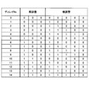
- FIG. 3 is a diagram illustrating a correspondence relationship between data held by the shift registers 40A and 40B connected to the delay adjustment circuits 10 and 50 of the comparative example and a delay number (delay number) corresponding to the delay time of the delay adjustment circuit. It is.
- the selection signal is input from the shift registers 40A and 40B to the selectors 21 to 25 and 61 to 63 (see FIGS. 1A and 1B) of the delay adjustment circuits 10 and 50.
- the selection signal has 5-bit data for fine adjustment and 3-bit data for coarse adjustment.
- the data of each bit is output from the shift registers 40A and 40B as a selection signal.
- a description will be given by assigning 0 to 14 delay numbers (delay numbers) to a set of 8-bit selection signals.
- All 8-bit selection signals with delay number 0 are set to "0". From delay number 0 to delay number 4, the selection signal for coarse adjustment is fixed at “0”, and the 5-bit selection signal for fine adjustment is set so that “1” rises sequentially from the left bit. Has been.
- the delay time given by the selection signal of delay number 0 is 120 ps obtained by adding 20 ps in the delay adjustment circuit 10 to 100 ps in the delay adjustment circuit 50. Each time the delay number increases by one, the delay amount in the fine adjustment delay adjustment circuit 10 increases by 20 ps. Therefore, the delay time given by the selection signal of delay number 4 is 200 ps.
- the delay time given by the selection signal of delay number 5 is 220 ps obtained by adding 20 ps in the delay adjustment circuit 10 to 200 ps in the delay adjustment circuit 50.
- the fine adjustment bit and the coarse adjustment bit are set so as to sequentially rise from “0” to “1”, and the delay given by the selection signal of the delay number 14
- the time is 400 ps obtained by adding 100 ps in the delay adjustment circuit 10 to 300 ps in the delay adjustment circuit 50.
- FIG. 4A is a diagram showing a delay adjustment circuit 10A in which a power saving mechanism for stopping an inverter and a selector not included in the signal propagation path is added to the delay adjustment circuit 10 shown in FIG.
- the delay adjustment circuit 10A has basically the same circuit configuration as the delay adjustment circuit 10 of the comparative example shown in FIG. 1A, but fixed data is input instead of data X to one input terminal of the selector 25. The point is different. Although the fixed data “0” is input to the delay adjustment circuit 10A illustrated in FIG. 4A, the fixed data may be “1”.
- the selection signal input to the selector located behind the selector that is the turning point when viewed from the input terminal IN and the output terminal OUT is set to “1”. This is because the signal input to the return side inverter and selector not included in the signal propagation path is switched from the data propagating through the forward side inverters 11 to 15 to the fixed data input to the selector 25. This is to save power by stopping the operation of the return-side inverter and selector that are not included in the path.
- selection signals “1”, “0”, “1”, “1”, “1” are input to the selectors 21 to 25 of the delay adjustment circuit 10A, they are input to the input terminal IN.
- the signal is turned back by the selector 22 as indicated by an arrow.
- the selector 25 outputs fixed data, and the fixed data output from the selector 25 propagates to the inverter 35, the selector 24, the inverter 34, the selector 23, and the inverter 33.
- the data based on the fixed data input to the selector 25 is invalid data (invalid data) regardless of the data based on the signal input from the input terminal IN.
- the delay adjustment circuit 10A having the power saving mechanism when the signal turning point shifts to the back side when viewed from the input terminal IN and the output terminal OUT, an inverter or selector that holds invalid data in the signal propagation path is provided. To be included. For this reason, while invalid data propagates in the signal path, there arises a problem that a signal input to the input terminal IN does not propagate accurately to the output terminal OUT.
- Such a problem is particularly caused by the coarse adjustment delay obtained by adding a power saving mechanism to the coarse adjustment delay adjustment circuit 50 (see FIG. 1B) of the comparative example in addition to the delay adjustment circuit 10A shown in FIG. 4A. This is noticeable when the adjustment circuit is used.
- the return point of the signal in the delay adjustment circuit 10A is simply reduced by 20 ps. Shifting from the selector 21 to the selector 25 toward the back as viewed from the input terminal IN and the output terminal OUT.
- the signal delay device of the comparative example including the delay adjustment circuit as described above, for example, when the data signal is captured in an information processing device such as a server, the capture timing of the capture signal is an appropriate timing with respect to the data signal. In order to delay the data signal or the capture signal.
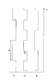
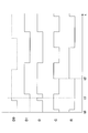
- FIG. 5 to FIG. 8 are timing charts showing an operation when a data signal is taken.
- the data signal is represented as D (abbreviation of Data)
- the capture signal is represented as C (abbreviation of Capture)
- the signal representing the capture result is represented as R (abbreviation of Result).
- the horizontal axis is the time axis, and the right direction is the time advance direction.
- the data signal D is captured at the rising edge of the capture signal C.
- the period of the capture signal C shown in FIG. 5 is set to half of the data signal D as an example.
- the rising edge of the capture signal C indicated by the arrow A is adjusted so as to be positioned near the center of the period B where the data signal D is at the H (High) level.
- the Such adjustment is realized by delaying the data signal D or the capture signal C.
- the signal R representing the capture result captures the data signal D at the rise timing of the capture signal C, the signal R is accurately captured in the example of FIG.
- the delay adjustment circuit 10 does not have a power saving mechanism.
- the delay adjustment circuit 10 When the selection signal “1”, “0”, “0”, “0”, “0” is input to the delay adjustment circuit 10 (see FIG. 1A), the data signal output from the output terminal OUT is D0, the selection signal A data signal output from the output terminal OUT when “1”, “1”, “0”, “0”, “0” is input is represented by D1. Since the waveform of the data signal D1 has a larger delay amount than the data signal D0, it is shifted to the right of the waveform of the data signal D0.
- the data signal D becomes equal to the data signal D0.
- the data signal D becomes a data signal D1 having a larger delay amount than the data signal D0.
- the data signal D has a waveform obtained by synthesizing the data signal D0 from time t0 to t1 and the data signal D1 after time t1.
- the data signal D0 is at the H level and the data signal D1 is at the L level. Therefore, the data signal D is at the H level for a period shorter than the cycle of the data signal D immediately before the time t1. Including a glitch.
- the center of the period in which the data signal D is at the H level is located at substantially the center of the capture signal C. Therefore, even if the data signal D is captured at time t2, the data R is represented as a signal R representing the capture result. A glitch near the rising edge of the signal D is not captured.
- the signal R representing the capture result has a signal waveform in which the data signal D is accurately captured.
- the operation example shown in FIG. 7 is an operation example when the delay amount is increased in the delay adjustment circuit 10 shown in FIG. 1, similarly to the operation example shown in FIG.
- the delay adjustment circuit 10 does not have a power saving mechanism.
- data signals D0 and D1 shown in FIG. 7 are the same as the data signals D0 and D1 shown in FIG.
- the data signal D becomes equal to the data signal D0.
- the data signal D is switched to the data signal D1 having a larger delay amount than the data signal D0, and the data
- the waveform of the signal D is a waveform obtained by synthesizing the waveform of the data signal D0 from time t0 to t1 and the waveform of the data signal D1 after time t1.
- the data signals D0 and D1 are both at the H level. For this reason, the data signal D does not include a glitch.
- the data signal D is captured at the rising timing of the capture signal C at time t2.
- the rise of the capture signal C is a timing having a sufficient margin with respect to both the rise timing and the fall timing of the data signal D.
- the signal R representing the capture result has a signal waveform in which the data signal D is accurately captured.
- the data signal D0A shown in FIG. 8 has the same waveform as the data signal D0 shown in FIGS. 6 and 7, but the selection signal “1”, “0”, “1” is sent to the delay adjustment circuit 10A (see FIG. 4A). This is a data signal output from the output terminal OUT when “,” “1” and “1” are input.
- the data signal D1A shown in FIG. 8 is a selection signal input to the delay adjustment circuit 10A (see FIG. 4A) as “1”, “0”, “1”, “1”, “1” to “1”, This is a data signal output from the output terminal OUT immediately after switching to “1”, “0”, “1”, “1”. Since the data signal D1A is data immediately after the signal turning point is switched to the back side when viewed from the input terminal IN and the output terminal OUT, the data signal D1A is from the output terminal of the selector 23 to the output terminal of the inverter 33 shown in FIG. Contains invalid data included in between. In FIG. 8, the period during which this invalid data is output is expressed as Invalid.
- the delay amount of the data signal D1A with respect to the data signal D0A is equal to the delay amount of the data signal D1 with respect to the data signal D0 shown in FIGS.
- the data signal D becomes equal to the data signal D0A.
- the data signal D is a data signal having a larger delay amount than the data signal D0A after time t1.
- the data signal D includes a part of the invalid data of the data signal D1A.
- the signal R representing the capture result captures invalid data included in the data signal D.
- a signal representing the fetch result R may contain invalid data.
- a semiconductor circuit device manufactured by semiconductor manufacturing technology such as LSI, tends to increase power consumption due to an increase in circuit scale due to miniaturization.
- the power consumption of LSI is required to be reduced from the viewpoint of LSI cooling, environment, or battery duration.
- the selection signal is set so that the delay elements not included in the signal propagation path are stopped among the delay elements of a plurality of stages for generating the delay.
- FIG. 9 is a diagram illustrating an information processing apparatus including the signal delay apparatus according to the first embodiment.
- the information processing apparatus is a server 90
- a server 90 an embodiment in which the information processing apparatus is a server 90 will be described as an example.
- the server 90 includes an LSI (Large Scale Integrated Circuit) 91, a main storage device 92, and a magnetic disk device 93.
- the LSI 91 and the main storage device 92 and the main storage device 92 and the magnetic disk device 93 are connected to each other by, for example, dedicated input / output buses.
- the LSI 91 includes a processor core 94, an L1 (Level-1: primary) instruction cache 95, an L1 data cache 96, an L2 (Level-2: secondary) cache 97, a memory controller 98, and an I / O (Input / Output). Output) port 99.
- L1 Level-1: primary
- L1 data cache 96 L1 data cache 96
- L2 Level-2: secondary
- I / O I / O (Input / Output). Output) port 99.
- the processor core 94 is, for example, a CPU (Central Processing Unit) core (Core), and is an arithmetic processing device that performs arithmetic processing of the server 90 as an information processing device.
- the processor core 94, the L1 instruction cache 95, and the L1 data cache 96 may be integrated as a CPU.
- the L1 instruction cache 95 is a primary instruction cache that temporarily stores instructions necessary for the arithmetic processing of the processor core 94.
- an SRAM is used as the L1 instruction cache.
- the L1 data cache 96 is a cache memory that temporarily stores data necessary for the arithmetic processing by the processor core 94 or data generated by the arithmetic processing.
- the L2 cache 97 is a cache memory lower than the L1 instruction cache 95 and the L1 data cache 96 in the sense that it is close to the main storage device 92 in the memory hierarchical structure, and is typically an L1 instruction cache 95 and an L1 data cache. Although the processing speed is lower than 96, the cache memory has a large capacity.
- the L2 cache 97 is realized by an SRAM, for example.
- the memory controller 98 is a control device that performs control when the LSI 91 reads / writes data from / to the main storage device 92, and is realized by, for example, an LSI.
- the I / O port 99 inputs / outputs data between the memory controller 98 and the main storage device 92 when the LSI 91 performs data read / write control with the main storage device 92.
- the I / O port 99 includes the signal delay device of the first embodiment.
- the main storage device 92 is, for example, a DRAM (Dynamic Random Access Memory) or a ROM (Read Only Memory), and the magnetic disk device 93 is, for example, a hard disk.
- DRAM Dynamic Random Access Memory
- ROM Read Only Memory
- the server 90 may include a data input / output interface that communicates with an external device.
- FIG. 10 is a diagram illustrating the signal delay device according to the first embodiment.
- the signal delay device 100 includes a delay adjustment circuit 110, a selection signal generation unit 120, a shift register 130, a delay adjustment determination unit 140, a delay setting data generation unit 150, an OR circuit (logical sum circuit) 160, a change flag.
- An FF (FlipFFlop) 170 and an AND circuit (logical product circuit) 180 are included.
- the signal delay device 100 is a signal delay device that adjusts the delay amount of the capture signal C.
- the original signal C0 of the captured signal is input to the signal delay device 100, and the delay amount is adjusted.
- the delay adjustment circuit 110 includes a delay adjustment circuit 110A for fine adjustment and a delay adjustment circuit 110B for coarse adjustment, and delays (positive or negative delay) the original signal C0 of the captured signal input to the input terminal IN. And the capture signal C is output from the output terminal OUT. That is, the original signal C0 of the capture signal is an example of an input signal of the signal delay device 100, and the capture signal C is an example of a delay signal of the signal delay device 100.
- the delay adjustment circuit 110A for fine adjustment is basically the same as the delay adjustment circuit 10 for fine adjustment of the signal delay device of the comparative example (see FIG. 1A), and includes a forward side inverter, a selector, and a return side inverter. 4 stages.
- the forward-side inverter and the return-side inverter are an example of a delay unit connected in series.
- the selector is an example of a selection unit that outputs a delay signal of any inverter.
- the coarse adjustment delay adjustment circuit 110B includes two stages of a forward side inverter, a selector, and a return side inverter.
- the coarse adjustment delay adjustment circuit 110B has a larger delay adjustment range than the fine adjustment delay adjustment circuit 110A, but the circuit configuration is different only in the number of stages of the forward-side inverter, the selector, and the return-side inverter. Is basically the same as the delay adjustment circuit 110A for fine adjustment.
- the number of forward-side inverters, selectors, and return-side inverters may not be the same as shown in FIG. 1A.
- one selector is provided for a plurality of forward-side inverters. It may be.
- one selector may be provided for a plurality of inverters on the return side.
- the delay adjustment circuit 110A or 110B may have a circuit configuration including either a forward-side inverter or a return-side inverter.
- the delay adjustment circuit 110A for fine adjustment and the delay adjustment circuit 110B for coarse adjustment are connected in series, and the signal input from the input terminal IN of the delay adjustment circuit 110 is coarsely adjusted by the delay adjustment circuit 110B for coarse adjustment. And a fine adjustment delay is provided by the fine adjustment delay adjustment circuit 110A and output from the output terminal OUT.
- the selection signal generation unit 120 generates a selection signal for input to the delay adjustment circuit 110 based on the delay setting data held by the shift register 130.
- the circuit configuration of the selection signal generation unit 120 will be described later with reference to FIGS. 14A and 14B.
- the shift register 130 is an example of a data holding unit that holds delay setting data set by the delay setting data generation unit 150.
- the delay setting data is data to be set in the shift register 130 in order to determine the value of the selection signal generated by the selection signal generation unit 120, and the delay setting in order to adjust the delay amount in the delay adjustment circuit 110.
- the delay setting data includes delay setting data for fine adjustment and delay setting data for coarse adjustment.
- the fine adjustment delay setting data and the coarse adjustment delay setting data each have a bit width obtained by adding 1 to the number of selectors included in the delay adjustment circuits 110A and 110B.
- the delay setting data for fine adjustment is 5 bits
- the delay setting data for coarse adjustment is 3 bits. Therefore, the shift register 130 outputs 8-bit delay setting data.
- the output of the AND circuit 180 is input to the shift register 130.
- the delay setting data held by the shift register 130 is updated when the output of the AND circuit 180 becomes “1”.
- the shift register 130 and the delay setting data will be described later with reference to FIGS. 14A, 14B, 15A, and 15B.
- the delay adjustment determination unit 140 compares the phase of the data signal D and the phase of the capture signal C, and it is necessary to increase (+) the delay amount, decrease ( ⁇ ) the delay amount, or Then, it is determined whether adjustment of the delay amount is necessary, and the determination result is output.
- the delay adjustment determination unit 140 outputs a delay increase signal (+) and a delay decrease signal ( ⁇ ) representing the determination result.
- the determination result that the delay increase signal (+) is “1” (H level) and the delay decrease signal ( ⁇ ) is “0” (L level) indicates that the delay amount needs to be increased.
- the determination result that the delay increase signal (+) is “0” (L level) and the delay decrease signal ( ⁇ ) is “1” (H level) indicates that the delay amount needs to be decreased.
- a detailed circuit configuration of the delay adjustment determination unit 140 will be described later with reference to FIG.
- the delay setting data generation unit 150 receives the delay increase signal (+) and the delay decrease signal ( ⁇ ) output from the delay adjustment determination unit 140.
- the delay setting data generating unit 150 generates a delay increasing signal (+) and a delay decreasing signal ( ⁇ ) based on the delay increasing signal (+) and the delay decreasing signal ( ⁇ ) and the delay setting data currently set in the shift register 130. Generate delay setting data reflecting the contents of-).
- the detailed circuit configuration of the delay setting data generation unit 150 will be described later with reference to FIG.
- the OR circuit 160 outputs a logical sum of the delay increase signal (+) and the delay decrease signal ( ⁇ ) output from the delay adjustment determination unit 140.
- the output of the OR circuit 160 is “1” if either the delay increase signal (+) or the delay decrease signal ( ⁇ ) is “1” (H level).
- the output of the OR circuit 160 is input to the change flag FF170.
- the change flag FF170 sets a change flag at the rising edge of the clock based on the output of the OR circuit 160.
- the change flag FF170 is an example of a logical sum holding unit that holds a calculation result of an OR circuit 160 as an example of a logical sum calculation circuit.
- the change flag is a flag used when changing the signal turn-back point in the delay adjustment circuit 110.
- the change flag is set to “0” (L level: off) when the signal return point is not switched, and is set to “1” (H level: on) when the signal return point is switched.
- the change flag becomes “1” (H level: ON) if either the delay increase signal (+) or the delay decrease signal ( ⁇ ) is “1” (H level).
- the change flag is “0” (L level: off) when both the delay increase signal (+) and the delay decrease signal ( ⁇ ) are “0” (L level).
- the change flag is input to the selection signal generation unit 120 and the AND circuit 180.
- the signal delay device 100 of the first embodiment turns on the power saving mechanism when the change flag is “0” (off), and turns off the power saving mechanism when the change flag is “1” (on).
- the on / off of the power saving mechanism is switched by a selection signal set based on the delay setting data and the change flag.
- the on / off of the power saving mode in the signal delay device 100 according to the first embodiment will be described later with reference to FIGS. 15A and 15B.
- the AND circuit 180 receives the clock and the change flag, and outputs a logical product of the value corresponding to the clock level and the value of the change flag.
- the output of the AND circuit 180 is input to the shift register 130.
- the delay setting data held by the shift register 130 is updated to new delay setting data generated by the delay setting data generation unit 150 when the output of the AND circuit 180 becomes “1”.
- the delay adjustment determination unit 140 determines that the delay amount of the captured signal C needs to be increased or decreased, and increases the delay increase signal (+) or the delay decrease signal ( ⁇ ). Is output, the delay setting data generation unit 150 generates new delay setting data.
- the delay adjustment determination unit 140 outputs the delay increase signal (+) or the delay decrease signal ( ⁇ )
- the change flag FF170 raises the change flag with the rise of the clock.
- the change flag is input to the selection signal generation unit 120 and to one input terminal of the AND circuit 180.
- the signal delay device 100 turns off the power saving mechanism of the delay adjustment circuit 110.
- the reason why the signal delay device 100 turns off the power saving mechanism is to reset the selection signal as preparation for switching the signal return point.
- the selection signal output from the selection signal generation unit 120 is updated.
- the return point of the signal in the delay adjustment circuit 110 is changed, and the capture signal C whose delay amount is adjusted from the output terminal OUT of the delay adjustment circuit 110 is a signal for capturing the data signal D in the delay adjustment determination unit 140. As output.
- the signal delay device 100 turns off the power saving mechanism when the change flag rises with the rise of a certain clock.
- the reason for turning off the power saving mechanism when the change flag rises is to remove invalid data in the delay adjustment circuit 110 before the next clock rises in preparation for the case where invalid data exists in the delay adjustment circuit 110. This is to provide a preparation period for doing this.
- the signal delay device 100 changes the return point of the signal, and takes the captured signal C whose delay amount is adjusted into the delay adjustment circuit. 110 from the output terminal OUT.
- the delay adjustment determination unit 140 determines that the delay amount of the captured signal C needs to be increased or decreased and the change flag is raised. There is an interval of one clock cycle before the change.
- This interval of one clock cycle is provided as a preparation period for removing invalid data that may be generated in the delay adjustment circuit 110 by the power saving mechanism.
- the OR circuit 160, the change flag FF170, and the AND circuit 180 are an example of a preparation period setting unit that sets a preparation period.
- FIG. 11 is a diagram illustrating a circuit configuration of the delay adjustment determination unit 140 of the signal delay device according to the first embodiment.
- the delay adjustment determination unit 140 includes an input terminal 141A, an input terminal 141B, a delay unit 142, an FF 143, an FF 144, a delay unit 145, an EOR (exclusive OR) circuit 146, a delay unit 147, a NOR (negative OR) circuit 148, An output terminal 149A and an output terminal 149B are included.
- the input terminal 141A is connected to the delay unit 142.
- the delay unit 142 receives the capture signal C from the input terminal 141A.
- the delay unit 142 includes a buffer 142A and an inverter 142B.
- the output terminal of the delay unit 142 is connected to the clock input terminal CK of the FF 143 and the clock input terminal CK of 143.
- the delay unit 142 outputs a signal C1 obtained by delaying the capture signal C input from the input terminal 141A.
- the delay time by the buffer 142A and the inverter 142B of the delay unit 142 is, for example, the sum of the time from when the data signal D is input to the input terminal 141B until it is output from the EOR circuit 146 and the setup time of the FF 143. It is set to be the same as the time.
- the setup time is a time indicating how long the output circuit in the previous stage must continue to output the data signal to be held in the flip-flop before the timing at which the clock signal is input. .
- the FF 143 includes a clock input terminal CK, a data input terminal D, and a data output terminal Q.
- the clock signal input terminal CK is connected to the output terminal of the delay unit 142, and the signal C1 output from the delay unit 142 is input thereto.
- the data input terminal D is connected to the output terminal of the EOR circuit 146, and the data signal D1 output from the EOR circuit 146 is input thereto.
- the data output terminal Q is connected to one input terminal of the NOR circuit 148.
- the FF 143 takes the data signal D1 output from the EOR circuit 146 into the data input terminal D when the signal C1 input to the clock signal input terminal CK rises. Data taken in the data input terminal D is reflected in the data output terminal Q.
- the FF 144 includes a clock input terminal CK, a data input terminal D, and a data output terminal Q.
- the clock signal input terminal CK is connected to the output terminal of the delay unit 142, and the signal C1 output from the delay unit 142 is input thereto.
- the data input terminal D is connected to the output terminal of the delay unit 147, and receives the data signal D2 output from the delay unit 147.
- the data output terminal Q is connected to the other input terminal of the NOR circuit 148 and to the output terminal 149B.
- the FF 144 takes in the data signal D2 output from the delay unit 147 to the data input terminal D when the signal C1 input to the clock signal input terminal CK rises. Data taken in the data input terminal D is reflected in the data output terminal Q.
- the input terminal 141B is connected to one input terminal of the delay unit 145 and the EOR circuit 146.
- the data signal D is input to the input terminal 141B.
- the delay unit 145 includes buffers 145A and 145B.
- the output terminal of the delay unit 145 is connected to the other input terminal of the EOR circuit 146.
- the input terminal 141B is connected to one input terminal of the EOR circuit 146, and the output terminal of the delay unit 145 is connected to the other input terminal.
- the output terminal of the EOR circuit 146 is connected to the data input terminal D of the FF 143 and the input terminal of the delay unit 147.
- the EOR circuit 146 outputs an exclusive OR of the data signal input from the input terminal 141B and the data signal input from the delay unit 145.
- the data signal D is input to the two input terminals of the EOR circuit 146, but one data input signal is input with a delay of the delay time of the delay unit 145. Therefore, when the signal level of the data signal is switched, the values of the two input data of the EOR circuit 146 are different during the delay time of the delay unit 145, so that the EOR circuit 146 has the data signal D1 at the H level ("1"). Is output.
- the delay unit 145 and the EOR circuit 146 are rise detection circuits that detect the rise of the data input signal.
- the delay unit 147 includes buffers 147A and 147B.
- the output terminal of the delay unit 147 is connected to the data input terminal D of the FF 144.
- the data output terminal Q of the FF 143 is connected to one input terminal, and the data output terminal Q of the FF 144 is connected to the other input terminal.
- the output terminal of the NOR circuit 148 is connected to the output terminal 149A.
- the NOR circuit 148 outputs a negative OR of the data signal input from the data output terminal Q of the FF 143 and the data signal input from the data output terminal Q of the FF 144.
- FIG. 12 is a timing chart showing the operation of the delay adjustment determination unit 140 of the signal delay device according to the first embodiment.
- the period of the capture signal C is set to half of the data signal D as an example.
- the rising edge of the capture signal C is located at the center of the period in which the data signal D is at the H level or the L level. I decided to.
- the data signal D rises to the H level (“1”) at time t1
- the data signal D input to one input terminal of the EOR circuit 146 becomes “1”.
- the data signal input to the other input signal of the EOR circuit 146 becomes “1” after the delay time by the delay unit 145. Therefore, the EOR circuit 146 outputs the data signal D1 at the H level (“1”) between the time t2 and the time t5.
- the width of the pulse when the data signal D1 is at the H level (“1”) corresponds to the delay time of the delay unit 145.
- the data signal D1 is delayed by the delay time in the delay unit 147, and is output from the delay unit 147 as the data signal D2.
- the data signal D2 rises at time t4 and falls at time t6.
- the time difference between time t2 and time t4 corresponds to the delay time of the delay unit 147.
- the capture signal C falls at time t1, it is delayed by the delay unit 142 and output as the signal C1. For this reason, the signal C1 rises at time t3.
- the time difference from time t1 to time t3 corresponds to the delay time of the delay unit 142.
- the above operation is the same even after the data signal D falls at time t7. From time t6 to time t12, the same operation as from time t1 to time t6 is performed.
- the output terminal 149A outputs a delay increase signal (+) representing a determination result that requires an increase (+) in the delay amount, and the output terminal 149B represents a determination result that requires a decrease ( ⁇ ) in the delay amount. Outputs a delay reduction signal (-).
- the delay increase signal (+) is “1” and the delay decrease signal ( ⁇ ) is “0”, the delay amount of the capture signal C needs to be increased (+).
- the delay increase signal (+) is “0” and the delay decrease signal ( ⁇ ) is “1”, the delay amount of the capture signal C needs to be decreased ( ⁇ ).
- the data signal D2 is at the H level (“1”) from the time t4 to the time t6.
- the value of the data signal D2 is reflected on the output terminal 149B via the FF 144. That is, the output value of the output terminal 149B is “1”. Further, during the period from time t4 to time t6, the output of the NOR circuit 148 is “0”, and the output value of the value of the output terminal 149A is “0”.
- the period from time t4 to time t6 is a period in which the adjustment of the delay amount of the capture signal C needs to be reduced (-).
- the NOR circuit 148 since the data signals D1 and D2 are both at the L level (“0”) from the time t6 to the time t8, the NOR circuit 148 becomes “1”. That is, the output value of the output terminal 149A is “1”. Further, since the data signal D2 is “0”, the data output terminal Q of the FF 144 outputs L level (“0”) again. That is, the output value of the output terminal 149B is “0”.
- the period from time t6 to time t8 is a period in which the adjustment of the delay amount of the capture signal C needs to be increased (+).
- the delay adjustment determination unit 140 compares the phases of the data signal D and the capture signal C and needs to increase (+) the delay amount or decrease ( ⁇ ) the delay amount. It is determined whether there is a delay amount adjustment or not, and the determination result is output.
- FIG. 13 is a diagram illustrating a circuit configuration of the delay setting data generation unit 150 of the signal delay device according to the first embodiment.
- the delay setting data generation unit 150 includes a + terminal and a ⁇ terminal to which a delay increase signal (+) and a delay decrease signal ( ⁇ ) are input from the delay adjustment determination unit 140 (see FIG. 10), respectively. Further, the delay setting data generation unit 150 receives input terminals IN0 to IN4 to which 5-bit delay setting data is input from the shift register 130 (see FIG. 10) and 5-bit delay setting data to the shift register 130, respectively. Output terminals OUT0 to OUT4 for outputting.
- the delay setting data input from the input terminals IN0 to IN4 represents the value of the current delay setting data held by the shift register 130 in order to generate four selection signals to be input to the delay adjustment circuit 110A for fine adjustment.
- the delay setting data output from the output terminals OUT0 to OUT4 and set in the shift register 130 represents delay setting data updated at the next rising edge of the clock signal.
- the delay setting data generation unit 150 has a circuit for generating 3-bit delay setting data for generating two selection signals to be input to the coarse adjustment delay adjustment circuit 110B, in addition to the circuit shown in FIG.
- the circuit configuration is the same except that the number of bits of the delay setting data to be handled is different.
- FIG. 13 shows a circuit that generates delay setting data for generating four selection signals to be input to the delay adjustment circuit 110A for fine adjustment.
- Delay setting data is set to “1” on the smaller side of the subscripts (0 to 4) of the input terminals IN0 to IN4 and output terminals OUT0 to OUT4, and is set to “0” on the larger side of the subscripts.
- the position where the value of the delay setting data is switched from “1” to “0” corresponds to a signal turning point. That is, the delay amount of the signal in the delay adjustment circuit 110A is determined by the position where the value of the delay setting data is switched from “1” to “0”.
- the values of the input terminal IN0 and the output terminal OUT0 corresponding to the delay setting data of the first bit are fixed to “1”.
- the values of the input terminal IN4 and the output terminal OUT4 corresponding to the fifth bit delay setting data are fixed to “0”.
- the output terminal OUT0 is connected to an H level power supply, and the output terminal OUT4 is grounded.
- the values of the delay increase signal (+) and the delay decrease signal ( ⁇ ) input to the + terminal and the ⁇ terminal respectively are “1” (H level) for the delay increase signal (+) and “0” for the delay decrease signal ( ⁇ ).
- “(L level) indicates that the delay amount is increased, and delay increase signal (+) is” 0 "(L level) and delay decrease signal (-) is” 1 "(H level). Represents reducing the amount.
- two-input NAND circuits (Negative AND circuits) 151A, 151B, and 151C and a three-input NAND circuit 151D are connected. Has been.
- two-input NAND circuits 152A, 152B, and 152C and a three-input NAND circuit 152D are connected between the + terminal, the ⁇ terminal, the input terminals IN0 and IN1, and the output terminal OUT2. .
- a two-input NAND circuit 153A, 153B, 153C and a three-input NAND circuit 153D are connected between the + terminal, the ⁇ terminal, the input terminals IN0 and IN1, and the output terminal OUT3.
- ENOR negative exclusive OR circuit 150A
- the output terminal of the ENOR circuit 150A is connected to one input terminal of each of the NAND circuits 151B, 152B, and 153B.
- one input terminal is connected to the + terminal, and the other input terminal is connected to the input terminal IN0.
- the output terminal of the NAND circuit 151A is connected to one input terminal of the NAND circuit 151D.
- NAND circuit 151B one input terminal is connected to the output terminal of ENOR circuit 150A, and the other input terminal is connected to input terminal IN1.
- the output terminal of the NAND circuit 151B is connected to one input terminal of the NAND circuit 151B.
- the NAND circuit 151C has one input terminal connected to the-terminal and the other input terminal connected to the input terminal IN2.
- the output terminal of the NAND circuit 151C is connected to one input terminal of the NAND circuit 151D.
- the output terminals of the NAND circuits 151A, 151B, and 151C are connected to three input terminals, and the output terminal is connected to the output terminal OUT1.
- the output terminals OUT2 and OUT3 are connected to the NAND circuits 152A to 152D and 153A to 153D in the same connection relationship as the NAND circuits 151A to 151D connected to the output terminal OUT1, respectively. Therefore, the description of the connection relationship between the NAND circuits 152A to 152D and 153A to 153D is omitted.
- the NAND circuit 151A outputs “0” because the value “1” of the delay increase signal (+) and the value “1” of the input terminal IN0 are input.
- the NAND circuit 151B Since the NAND circuit 151B receives the output “0” of the ENOR circuit 150A and the value of the input terminal IN1, the NAND circuit 151B outputs “1” regardless of the value of the input terminal IN1.
- the NAND circuit 151C Since the value “0” of the delay reduction signal ( ⁇ ) and the value of the input terminal IN2 are input, the NAND circuit 151C outputs “1” regardless of the value of the input terminal IN2.
- the output of the NAND circuit 151D is “1”. That is, the value of the output terminal OUT1 is “1”.
- the delay setting data of the second bit is the next clock signal.
- the value of the output terminal OUT1 is set to “1”.
- the NAND circuit 151A outputs “1” because the value “0” of the delay increase signal (+) and the value “1” of the input terminal IN0 are input.
- the NAND circuit 151B Since the NAND circuit 151B receives the output “0” of the ENOR circuit 150A and the value of the input terminal IN1, the NAND circuit 151B outputs “1” regardless of the value of the input terminal IN1.
- the NAND circuit 151C Since the NAND circuit 151C receives the value “1” of the delay decrease signal ( ⁇ ) and the value of the input terminal IN2, the NAND circuit 151C outputs “0” if the value of the input terminal IN2 is “1”. If the value of IN2 is “0”, “1” is output.
- the output of the NAND circuit 151D is “ 1 ". That is, the value of the output terminal OUT1 is “1”.
- the delay setting data of the second bit is the rising edge of the next clock signal.
- the value of the output terminal OUT1 is set to “0”.
- the NAND circuit 151A outputs “1” because the value “0” of the delay increase signal (+) and the value “1” of the input terminal IN0 are input.
- the NAND circuit 151B Since the NAND circuit 151B receives the output “1” of the ENOR circuit 150A and the value of the input terminal IN1, the NAND circuit 151B outputs “0” if the value of the input terminal IN1 is “1” and the value of the input terminal IN1. If “0”, “1” is output.
- the NAND circuit 151C Since the value “0” of the delay reduction signal ( ⁇ ) and the value of the input terminal IN2 are input, the NAND circuit 151C outputs “1” regardless of the value of the input terminal IN2.
- the value of the input terminal IN1 is “1”, “1”, “0”, and “1” are input to the three input terminals of the NAND circuit 151D, and thus the output of the NAND circuit 151D is “ 1 ". That is, the value of the output terminal OUT1 is “1”, and the value of the input terminal IN1 is output from the output terminal OUT1 without being changed.
- the value of the output terminal OUT1 is set according to the values of the delay increase signal (+) and the delay decrease signal ( ⁇ ) input to the + terminal and the ⁇ terminal, respectively.
- the value of the output terminal OUT1 is set to the same value “1” as the value “1” of the adjacent input terminal IN0.
- the delay amount is decreased, if the value of the adjacent input terminal IN2 is “0”, the value “0” is set to the same value as the value “0” of the adjacent input terminal IN2. Further, when maintaining the delay amount, the value of the input terminal IN1 is directly output from the output terminal OUT1.
- the 5-bit delay setting data set in the shift register is set by the operation as described above, and the delay amount in the delay adjustment circuit 110A is adjusted.
- FIG. 14A is a diagram illustrating a delay adjustment circuit 110A for fine adjustment, a selection signal generation unit 120, a shift register 130, and a change flag FF170 of the signal delay device 100 according to the first embodiment.
- FIG. 14B is a diagram illustrating a detailed circuit configuration of a part of the selection signal generation unit 120.
- the signal delay device 100 includes the delay adjustment circuit 110A for fine adjustment and the delay adjustment circuit 110B for coarse adjustment.
- the circuit configurations of the delay adjustment circuit 110A and the delay adjustment circuit 110B are basically the same except for the number of stages of the inverter and the selector.
- the detailed circuit configuration of the delay adjustment circuit 110A for fine adjustment and the selection signal generation unit 120, the delay adjustment circuit 110A, the selection signal generation unit 120, and the shift register 130 will be described with reference to FIGS. 14A and 14B.
- the operation of the change flag FF170 will be described.
- the delay adjustment circuit 110A is basically the same as the delay adjustment circuit 10 (see FIG. 1A) of the signal delay device of the comparative example, but the delay adjustment circuit 110A of the first embodiment 4 stages of inverters on the side, selectors, and inverters on the return side.
- the number of stages of the forward-side inverter, selector, and return-side inverter shown in FIG. 14A is merely an example, and may be an arbitrary number of stages. The same applies to the coarse adjustment delay adjustment circuit 110B (not shown in FIG. 14A).
- the delay adjustment circuit 110A includes inverters 11, 12, 13, and 14, selectors 21, 22, 23, and 24, and inverters 31, 32, 33, and 34.
- the inverters 11 to 14, the selectors 21 to 24, and the inverters 31 to 34 give a delay to the input signal.
- connection relationships of the inverters 11 to 14, the selectors 21 to 24, and the inverters 31 to 34 are as follows: the inverters 11 to 14, the selectors 21 to 24, and the inverters 31 to 34 included in the delay adjustment circuit 10 of the comparative example shown in FIG. Since it is the same, description of FIG. 1 is used and duplication description is abbreviate
- the selection signal input to the selectors 21 to 24 is generated by the selection signal generation unit 120.
- the selection signal generation unit 120 is a logic circuit that generates selection signals to be input to the selectors 21 to 24 of the delay adjustment circuit 110A based on the delay setting data held by the shift register 130.
- the selection signal generation unit 120 includes selection signal generation logic circuits 121, 122, 123, and 124 for fine adjustment of the delay amount.
- the selection signal generation logic circuits 121, 122, 123, and 124 are connected to a shift register 130 that holds delay setting data having a bit width obtained by adding 1 to the number of selection signal generation logic circuits 121, 122, 123, and 124. .
- the selection signal generation unit 120 includes two selection signal generation logic circuits for coarse adjustment of the delay amount, in addition to the configuration shown in FIG. 14A.
- the selection signal generation logic circuits 121, 122, 123, and 124 have the same circuit configuration, and include a NAND circuit 201 and a selector 202.
- the circuit configuration of the selection signal generation logic circuits 121, 122, 123, and 124 will be described later.
- the shift register 130 includes five delay setting FF1, delay setting FF2, delay setting FF3, delay setting FF4, and delay setting FF5 for fine adjustment of the delay amount.
- the shift register 130 holds 1-bit delay setting data in each of the delay setting FF1, the delay setting FF2, the delay setting FF3, the delay setting FF4, and the delay setting FF5. That is, the shift register 130 holds delay setting data having a bit width obtained by adding 1 to the number of selectors 21 to 24 of the delay adjustment circuit 110A.
- the shift register 130 includes three delay setting FFs for coarse adjustment of the delay amount in addition to that shown in FIG. 14A.
- the change flag FF 170 outputs a change flag to be input to the selection signal input terminal of each selector 202 of the selection signal generation logic circuits 121 to 124.
- the change flag FF170 sets the change flag at the rising edge of the clock based on the delay increase signal or the delay decrease signal.
- the output of the delay setting FF1 is input to one input terminal of the NAND circuit 201 of the selection signal generation logic circuit 121, and the output of the delay setting FF2 is inverted and input to the other input terminal.
- the output (negative logical product) of the NAND circuit 201 is input to one input terminal of the selector 202 of the selection signal generation logic circuit 121, and the output of the delay setting FF2 is input to the other input terminal.
- the change flag is input from the change flag FF 170 to the selection signal input terminal of the selector 202 of the selection signal generation logic circuit 121.
- the selector 202 selects and outputs the output of the NAND circuit 201 when the value of the change flag input from the change flag FF 170 is “0”, and the delay setting FF2 when the value of the change flag is “1”. Select and output the delay setting data.
- the output of the selector 202 of the selection signal generation logic circuit 121 is input as the selection signal 1 to the selector 21 of the delay adjustment circuit 110A.
- the output of the delay setting FF2 is input to one input terminal of the NAND circuit 201 of the selection signal generation logic circuit 122, and the output of the delay setting FF3 is inverted and input to the other input terminal.
- the output (negative logical product) of the NAND circuit 201 is input to one input terminal of the selector 202 of the selection signal generation logic circuit 122, and the output of the delay setting FF3 is input to the other input terminal.
- the change flag is input from the change flag FF 170 to the selection signal input terminal of the selector 202 of the selection signal generation logic circuit 122.
- the selector 202 selects and outputs the output of the NAND circuit 201 when the value of the change flag input from the change flag FF 170 is “0”, and the delay setting FF3 when the value of the change flag is “1”. Select and output the delay setting data.
- the output of the selector 202 of the selection signal generation logic circuit 122 is input as the selection signal 2 to the selector 22 of the delay adjustment circuit 110A.
- the output of the delay setting FF3 is input to one input terminal of the NAND circuit 201 of the selection signal generation logic circuit 123, and the output of the delay setting FF4 is inverted and input to the other input terminal.
- the output (negative AND) of the NAND circuit 201 is input to one input terminal of the selector 202 of the selection signal generation logic circuit 123, and the output of the delay setting FF4 is input to the other input terminal.
- the change flag is input from the change flag FF 170 to the selection signal input terminal of the selector 202 of the selection signal generation logic circuit 123.
- the selector 202 selects and outputs the output of the NAND circuit 201 when the value of the change flag input from the change flag FF 170 is “0”, and the delay setting FF 4 when the value of the change flag is “1”. Select and output the delay setting data.
- the output of the selector 202 of the selection signal generation logic circuit 123 is input as the selection signal 3 to the selector 23 of the delay adjustment circuit 110A.
- the output of the delay setting FF4 is input to one input terminal of the NAND circuit 201 of the selection signal generation logic circuit 124, and the output of the delay setting FF5 is inverted and input to the other input terminal.
- the output (negative logical product) of the NAND circuit 201 is input to one input terminal of the selector 202 of the selection signal generation logic circuit 124, and the output of the delay setting FF5 is input to the other input terminal.
- the change flag is input from the change flag FF 170 to the selection signal input terminal of the selector 202 of the selection signal generation logic circuit 124.
- the selector 202 selects and outputs the output of the NAND circuit 201 when the value of the change flag input from the change flag FF 170 is “0”, and the delay setting FF 5 when the value of the change flag is “1”. Select and output the delay setting data.
- the output of the selector 202 of the selection signal generation logic circuit 124 is input as the selection signal 4 to the selector 24 of the delay adjustment circuit 110A.
- selection signal generation logic circuits 121 to 124 can also be realized by the logic circuit shown in FIG. 14B.
- the selection signal generation logic circuit 121 will be described as a representative example.
- the selection signal generation logic circuit 121 includes AND circuits 211 and 212 and a NOR circuit 213.
- the output of the delay setting FF1 is input to one input terminal of the AND circuit 211, and the output of the delay setting FF2 is inverted and input to the other input terminal.
- the output of the delay setting FF2 is inverted and input to one input terminal of the AND circuit 212, and the change flag is input from the change flag FF170 to the other input terminal.
- the outputs (logical products) of the AND circuits 211 and 212 are input to the two input terminals of the NOR circuit 213, respectively.
- the NOR circuit 213 outputs a negative logical sum of the outputs of the AND circuits 211 and 212.
- the output of the NOR circuit 213 of the selection signal generation logic circuit 121 is equivalent to the output of the selector 202 of the selection signal generation logic circuit 121 shown in FIG. 14A and is input to the selector 21 as the selection signal 1.
- selection signals 2 to 4 are similarly input to the selectors 22 to 24 from the selector 202 of the selection signal generation logic circuits 122 to 124, respectively.
- delay setting data held by the shift register 130 will be described with reference to FIGS. 15A and 15B.
- FIG. 15A is a diagram illustrating an example of a correspondence relationship between delay setting data held by the shift register 130 of the signal delay device 100 according to the first embodiment and a delay number (delay number). The delay number corresponds to the delay time of the signal delay device 100.
- FIG. 15B is a diagram illustrating delay setting data held by the shift register 130 of the signal delay device 100 according to the first embodiment, together with a change flag and a selection signal.
- the delay setting data includes 5-bit data set in fine adjustment delay setting FF1 to delay setting FF5 and 3-bit data set in three delay setting FFs for coarse adjustment. Including.
- the 5-bit delay setting data set in the fine adjustment delay setting FF1 to the delay setting FF5 is stored in each of the fine adjustment selection signal generation logic circuits 121 to 124 (see FIG. 14A) in the selection signal generation unit 120. Entered. Similarly, the 3-bit delay setting data set in the three delay setting FFs for coarse adjustment is input to two selection signal generation logic circuits for coarse adjustment in the selection signal generation unit 120.
- the delay setting data for coarse adjustment and the delay setting data for fine adjustment are constructed such that the left data is “1” and the right data is “0”. Yes. Further, the delay setting data for coarse adjustment and the delay setting data for fine adjustment are respectively “1” as the delay number (delay number) increases for the same coarse adjustment delay setting data. The boundary between “0” and “0” is shifted to the right.
- the 3-bit delay setting data for coarse adjustment is fixed at “1”, “0”, and “0”.
- the 5-bit delay setting data for fine adjustment set in the delay setting FF1 to the delay setting FF5 starts from “1”, “0”, “0”, “0”, “0”, and the delay setting FF1.
- the delay setting data set in the delay setting FF4 is sequentially set to “1”.
- the delay number (delay No.) is 3
- the 5-bit delay setting data for fine adjustment is “1”, “1”, “1”, “1”, “1”, “0”.
- the 3-bit delay setting data for coarse adjustment is “1”, “1”, “0”, and the 5-bit delay setting data for fine adjustment is “1”, “0”. Return to ",” 0 ",” 0 ",” 0 ".
- the 3-bit delay setting data for coarse adjustment is fixed at “1”, “1”, “0”, and the 5-bit delay for fine adjustment As for the setting data, the delay setting data set from the delay setting FF1 to the delay setting FF4 is sequentially set to "1".
- the 5-bit delay setting data for fine adjustment is “1”, “1”, “1”, “1”, “0”.
- the delay setting data is input from the two delay setting FFs to the selection signal generation logic circuits 121 to 124 for fine adjustment shown in FIG. 14A, respectively, the input to the left input terminal for convenience of explanation. Is called left input, and input to the right input terminal is called right input.
- the outputs of the NAND circuit 201 in the selection signal generation logic circuits 121 to 124 are input to the selectors 21 to 24 as selection signals 1 to 4, respectively.
- the delay setting data is structured such that the left data is “1” and the right data is “0”.
- the output (selection signal) of the selection signal generation logic circuit (any of 121 to 124) in which the left input and the right input are “1” and “1” is “1”, and the delay setting is performed as described above.
- the data on the left side is “1”.
- the combination of delay setting data in which the left input and the right input are “1” and “1”, the signal input from the inverter (any one of 32 to 34) in the previous stage (right side in the figure) This is a combination of delay setting data for generating a selection signal to be input to the selector to be transmitted to the inverter (any one of 31 to 33) on the left side in the figure.
- the combination of the delay setting data in which the left input and the right input are “1” and “0” is a combination that is a boundary between 1 data and 0 data of the delay setting data.
- the output (select signal) of the selection signal generation logic circuit (any of 121 to 124) is “0”, so the left input and right input
- the output (selection signal) of the selection signal generation logic circuit (any of 121 to 124) is “1”, and the delay is as described above.
- the data on the right side is “0”.
- the combination of the delay setting data in which the left input and the right input are “0” and “0” ⁇ is located on the back side as viewed from the input / output terminals IN and OUT with respect to the selector serving as the signal return point.
- This is a combination of delay setting data for generating a selection signal input to the selector set in the power saving mode.
- the selection signal generation unit 120 illustrated in FIG. 14A detects a boundary of continuous 0 or 1 data included in the delay setting data, and 0 and 1 for determining the boundary position.
- the selection signal generated based on the data is output to a selector (any one of 21 to 24) corresponding to the delay amount of the delay signal.
- a boundary of continuous 0 or 1 data is a portion where the left input and the right input are “1” and “0” in the combination of delay setting data.
- the combination of delay data for which the left input and right input are “1" and "0" is a delay setting for generating a selection signal for generating a selector (any one of 21 to 24) that serves as a signal return point. It is a combination of data.
- the selection signal generation unit 120 illustrated in FIG. 14A generates a selection signal generated based on the logical product of 0 data and 1 data specifying the boundary position.
- An output signal from an inverter (any one of 12 to 14) corresponding to a delay amount equal to or greater than the delay amount is output to a selector (any one of 22 to 24).
- the left input and the right input are “0” and “0” for the selector (any one of 22 to 24) located on the back side as viewed from the input / output terminals IN and OUT with respect to the selector serving as the signal return point.
- “A selection signal that is generated based on a combination of delay setting data that becomes a trap is input.
- the delay amount in the delay adjustment circuit 110 can be controlled by sequentially shifting the delay setting data shown in FIG.
- the selector 21 is a signal return point in the delay adjustment circuit 110A for fine adjustment, and similarly, in the delay adjustment circuit 110B for coarse adjustment.
- the selector on the near side as viewed from the input / output terminal serves as a signal return point. Therefore, the delay time when the delay number (delay No.) is 0 is 100 ps obtained by adding 80 ps for coarse adjustment to 20 ps for fine adjustment.
- the selector 24 becomes a signal turn-back point in the fine adjustment delay adjustment circuit 110A.
- the delay adjustment circuit 110B for coarse adjustment two stages are provided.
- the selector on the back side when viewed from the input / output terminal serves as a signal return point. Therefore, when the delay number (delay No.) is 7, the delay time is 240 ps obtained by adding 160 ps for coarse adjustment to 80 ps for fine adjustment.
- the delay amount can be adjusted from 100 ps to 240 ps.
- the delay setting data is data having a value of “0” or “1” as described above.
- a negative operation unit that performs a negative operation is added to the selection signal generation unit 120 or the shift register 130.
- delay setting data delay setting data obtained by inverting “0” and “1” may be used.
- the delay setting data is 5-bit data set in the delay setting FF1 to the delay setting FF5, and is input to each of the selection signal generation logic circuits 121 to 124.
- the selection signal generation logic circuit 121 receives delay setting data from the delay setting FF1 located on the left side and the delay setting FF2 located on the right side.
- the delay setting data held by the delay setting FF1 and the delay setting FF2 are represented as left input and right input.
- the delay setting data held by the delay setting FF2 and the delay setting FF3 are represented as left input and right input.
- the delay setting data held by the delay setting FF3 and the delay setting FF4 are represented as left input and right input.
- the delay setting FF4 and the delay setting FF5 are provided. The delay setting data to be held is expressed as left input and right input.
- the selection signal generation logic circuits 121 to 124 perform the same operation for the change flag, the left input, and the right input. Therefore, in the description of FIG. 15B, the description is made without distinguishing the NAND circuit 201 and the selector 202 included in the selection signal generation logic circuits 121 to 124, and the selection signals 1 to 4 are not distinguished. Called.
- the output of the NAND circuit 201 is “1”.
- the selector 202 selects the output of the NAND circuit 201, and therefore the selection signal output from the selector 202 is “1”.
- the selector corresponding to the selection signal generation logic circuit in which the left input and the right input are “1” and “0” is a selector that serves as a signal return point.
- the change flag is “0”
- the left input and the right input are “0” and “0” when the signal is turned back when viewed from the input / output terminals IN and OUT of the delay adjustment circuit 110.
- the selector (any one of 22 to 24) in the delay adjustment circuit 110A for fine adjustment is set to the power saving mode.
- the output of the NAND circuit 201 is “0”.
- the change flag is “0”
- the selector 202 selects the output of the NAND circuit 201
- the selection signal output from the selector 202 is “0”. Further, the selection signal becomes “0” is a selection signal input to a selector (any one of 21 to 24) that is a signal turning point.
- the selector (21 to 24) that is the signal return point in the delay adjustment circuit 110 ) Is a combination of delay setting data for the selection signal generation logic circuit (any one of 121 to 124) that inputs the selection signal.
- the output of the NAND circuit 201 is “1”.
- the change flag is “0”, since the selector 202 selects the output of the NAND circuit 201, the selection signal output from the selector 202 is “1”.
- the change flag is “1”
- the selector 202 in the selection signal generation logic circuits 121 to 124 outputs the right input as it is as the selection signal, so the left input is irrelevant. Therefore, in FIG. 15B, the left input when the change flag is “1” is indicated by X.
- the right input may be “0” as seen from the selector (any one of 21 to 24) or the input / output terminals IN and OUT as shown in FIG. 15A.
- a selection signal generation logic circuit (any one of 122 to 124) for inputting a selection signal to a selector (any one of 21 to 24) located behind the signal turning point.
- the change flag is set to “1” when the selector that becomes the signal return point is changed.
- the change flag when the change flag is “1”, the right input becomes “0” because the selector (any one of 21 to 24) that becomes a new signal return point or the input / output terminals IN and OUT A selection signal generation logic circuit (any one of 122 to 124) that inputs a selection signal to a selector (any one of 21 to 24) that is newly behind the signal turn-back point as viewed from FIG.
- the selection signal is “1”. Further, when the change flag is “1”, it is a time to change the signal turning point.
- the change flag is “1”
- the right input becomes “1” when the signal return point is changed when the selector (21 to 21) on the near side of the new signal return point is changed.
- 23) is a selection signal generation logic circuit (any one of 121 to 123) for inputting a selection signal to any one of them.
- the selection signals 1 to 4 are set using the delay setting data and the change flag shown in FIG. 15B, and the power saving mode is switched.
- the process illustrated in FIG. 16 is a process realized by the signal delay device 100 illustrated in FIG. 10 and represents a control method of the signal delay device 100.
- FIG. 16 is a flowchart showing processing in the signal delay device 100 according to the first embodiment.
- the signal delay device 100 determines whether or not the phase difference between the data signal D and the capture signal C is appropriate (step S101). .
- Whether or not the phase difference is appropriate is determined by whether or not the delay adjustment determination unit 140 (see FIG. 11) is within a predetermined range before and after the center of the half cycle of the data signal D. This is done by determining whether or not.
- the signal delay device 100 determines whether or not the change flag is on (step S102). Whether or not the change flag is on is determined based on the value of the change flag output from the change flag FF 170 or the value of the change flag input to the selection signal generation unit 120.
- step S102 If it is determined in step S102 that the change flag is not on (S102: NO), the signal delay device 100 proceeds to step S103, and turns on the change flag at the rising edge of the clock signal (step S103).
- step S101 it is determined in step S101 that the phase difference is not appropriate, and it is determined in step S102 that the change flag is off. Therefore, the change flag is turned on in order to prepare for the change of the signal return point. .
- step S104 the signal delay device 100 turns off the power saving mechanism.
- the signal delay device 100 determines whether or not all the processes are finished when the process of Step S104 is finished (Step S106). The process is terminated when the operation of the signal delay device 100 is terminated.
- the signal delay device 100 determines whether or not the phase difference is appropriate again in step S101, but after determining that the phase difference is not appropriate in step S101 one cycle before, the signal return point is still changed. Therefore, even in step S101 of the second cycle, it is determined that the phase difference is not appropriate (step S101). As a result, the flow proceeds to step S102.
- the signal delay device 100 determines whether or not the change flag is turned on again in step S102 of the second cycle (step S102). Since the signal delay device 100 turns on the change flag in step S103 of the first cycle, it is determined that the change flag is on (step S102 YES) in step S102 of the second cycle. As a result, the flow proceeds to step S105.
- the signal delay device 100 changes the return point of the signal (step S105). Thereby, for example, the selection signals 1 to 4 are switched from “0”, “1”, “1”, “1” to “1”, “0”, “1”, “1”, and the signal turn-back point Is changed from the selector 21 to the selector 22.
- the signal delay device 100 turns on the change flag in step S103 in the first cycle and then changes the signal return point in step S105 in the second cycle. An interval is provided.
- the data signal is obtained by using the capture signal C after changing the signal turning point. If captured, the data signal can be accurately captured.
- the signal delay device 100 determines whether or not all the processes are finished when the process of Step S105 is finished (Step S106). The process is terminated when the operation of the signal delay device 100 is terminated.
- the signal delay device 100 determines whether or not the phase difference is appropriate in step S101 in the third cycle (step S101).
- step S107 if the phase difference is appropriate (YES in S101), the signal delay device 100 proceeds the flow to step S107. On the other hand, if the phase difference is not appropriate (NO in S101), the signal delay device 100 proceeds to steps S102 and S105, and steps S101, S102, and S105 until it is determined in step S101 that the phase difference is appropriate. , S106 is repeatedly executed.
- step S101 If it is determined in step S101 that the phase difference is appropriate (S101 YES), the signal delay device 100 turns off the change flag (step S107). Since the delay amount of the captured signal C becomes an appropriate value and it is no longer necessary to change the signal return point, the signal delay device 100 turns off the change flag.
- the signal delay device 100 turns on the power saving mechanism (step S108). After the change of the signal return point is completed, the power saving mechanism is turned on again to reduce power consumption.
- FIG. 17 is a timing chart showing the relationship between the delay setting data and the selection signal in the delay adjustment circuit 110A for fine adjustment of the signal delay device 100 of the first embodiment.
- the signal return point of the signal delay device 100 is the selector 21 and the power saving mechanism is on, so that the selection signal 1 is “0” and the selection signals 2 to 4 are “ 1 ".
- the delay increase signal (+) rises to “1”. Note that the delay reduction signal ( ⁇ ) remains “0”.
- the predetermined threshold value is, for example, a value representing a phase difference between the data signal D and the captured signal C when the rising edge of the captured signal C is within a predetermined range before and after the center of the half cycle of the data signal D. Is set.
- the signal return point is the selector 21 and the power saving mechanism is on, so that invalid data exists between the output terminal of the selector 24 and the output terminal of the inverter 32. .
- the delay setting FF2 of the shift register 130 becomes “1” at time t16 in order to change the return point of the signal. That is, the delay setting data is shifted from delay number 0 shown in FIG. 15A to delay number 1.
- the selection signal 1 becomes “1” at time t17.
- the output signal of the selector 22 is propagated to the selector 21 through the inverter 32. For this reason, as indicated by an arrow A in the figure, the falling edge of the output signal of the selector 22 propagates to the output signal of the selector 21 as a falling edge.
- the delayed output signal of the selector 21 delays the capture signal C output from the output terminal OUT of the delay adjustment circuit 110 as indicated by an arrow B.
- the rising edge of the capture signal C is positioned at the center of the half cycle of the data signal D.
- the delay increase signal (+) falls when the phase difference between the data signal D and the capture signal C falls below a predetermined threshold at time t18. That is, the phase difference between the data signal D and the capture signal C is determined to be larger than the predetermined threshold value between the times t11 and t18 when the delay increase signal (+) is at the H level.
- the change flag is turned off at time t20.
- the power saving mechanism When the change flag is turned off, the power saving mechanism is turned on, so that the fixed data is sent to the selectors 23 and 24 on the back side of the selector 22 that is the turning point when viewed from the input / output terminals IN and OUT of the delay adjustment circuit 110.
- the selection signal 3 and the selection signal 4 become “1” at time t21.
- the delay setting FF2 by the delay number 1 is “1”, and the delay setting FF3 is “0”.
- the signal turn-back point remains the selector 22 and remains unchanged.
- the signal delay device 100 turns off the power saving mechanism when the phase difference between the data signal D and the capture signal C exceeds a predetermined threshold, and the time corresponding to one clock cycle has elapsed. After that, the signal turning point is changed.
- invalid data can be removed while waiting for a period of one clock cycle (preparation period), and invalid data is captured by capturing the data signal D using the capture signal C with the adjusted delay.
- the correct data signal D can be captured.
- the server 90 including the signal delay device 100 according to the first embodiment in the I / O port 99 can suppress malfunction due to fetching invalid data, and can improve the stability and reliability of the operation.
- the signal delay device 100 including the delay adjustment circuit 110 for fine adjustment has been described.
- the delay adjustment circuit for coarse adjustment is included, the signal path may change greatly even if the delay amount is finely adjusted. Therefore, the coarse adjustment is controlled in the same way as the delay adjustment circuit 110 for fine adjustment. If the delay adjustment circuit is included, it is possible to provide a signal delay device in which the adjustment range of the delay amount can be increased and the stability and reliability of the operation are further improved.
- the signal delay device 100 turns on the power saving mechanism again when the change of the signal return point is completed, so that the signal delay device 100 can save power. .
- the signal delay device 100 according to the first embodiment is used for the I / O port 99 (see FIG. 9), the power saving of the server 99 can be achieved.
- the first embodiment it is possible to provide a signal delay device that achieves both reduction in power consumption and accuracy of an output signal, and a control method for the signal delay device.
- FIG. 18 is a diagram illustrating a signal delay device according to the second embodiment.
- the signal delay device 200 includes a delay adjustment circuit 110A, a selection signal generation unit 220, a shift register 230, a delay adjustment determination unit 140, and a delay setting data generation unit 150.
- the signal delay device 200 according to the second embodiment is different from the signal delay device 100 according to the first embodiment in that the OR circuit 160, the change flag FF 170, and the AND circuit 180 (see FIG. 10) are not included.
- the selection signal generation unit 220 generates a selection signal to be input to the delay adjustment circuit 110A based on the delay setting data held by the shift register 230.
- the selection signal generation unit 220 is not input with the value of the change flag unlike the selection signal generation unit 120 of the first embodiment, so that the selection signal generation unit 220 operates only with the delay setting data input from the shift register 230. Different from the signal generator 120.
- the circuit configuration of the selection signal generation unit 220 will be described later with reference to FIG.
- the shift register 230 holds delay setting data set by the delay setting data generation unit 150.
- the shift register 230 is different from the shift register 130 of Embodiment 1 in that the clock is directly input and the delay setting data is updated at the rising edge of the clock.
- FIG. 19 is a diagram illustrating a circuit configuration of the delay adjustment circuit 110A, the selection signal generation unit 220, and the shift register 230 of the signal delay device 200 according to the second embodiment.
- the selection signal generation unit 220 includes selection signal generation logic circuits 221, 222, 223, and 224.
- the selection signal generation logic circuits 221, 222, 223, and 224 are connected to a shift register 230 that holds bit width delay setting data obtained by adding 1 to the number of selection signal generation logic circuits 221, 222, 223, and 224. .
- the selection signal generation logic circuits 221, 222, 223, and 224 have the same circuit configuration, and include a NAND circuit 251 and a buffer 252.
- the buffer 252 is an example of a delay circuit that outputs an input signal with a delay.
- an element whose input / output delay time corresponds to about one cycle of the clock in the signal delay device 100 of Embodiment 1 may be used.
- the shift register 230 includes five delay setting FF1, delay setting FF2, delay setting FF3, delay setting FF4, and delay setting FF5.
- the output of the delay setting FF1 is input to one input terminal of the NAND circuit 251 of the selection signal generation logic circuit 221, and the output of the delay setting FF2 is inverted and input to the other input terminal via the buffer 252.
- the output signal of the NAND circuit 251 of the selection signal generation logic circuit 221 is input as the selection signal 1 to the selection signal input terminal of the selector 21 of the delay adjustment circuit 110A.
- the output of the delay setting FF 2 is input to one input terminal of the NAND circuit 251 of the selection signal generation logic circuit 222, and the output of the delay setting FF 3 is inverted and input to the other input terminal via the buffer 252.
- the output signal of the NAND circuit 251 of the selection signal generation logic circuit 222 is input as the selection signal 2 to the selection signal input terminal of the selector 22 of the delay adjustment circuit 110A.
- the output of the delay setting FF3 is input to one input terminal of the NAND circuit 251 of the selection signal generation logic circuit 223, and the output of the delay setting FF4 is inverted and input to the other input terminal via the buffer 252.
- the output signal of the NAND circuit 251 of the selection signal generation logic circuit 223 is input as the selection signal 3 to the selection signal input terminal of the selector 23 of the delay adjustment circuit 110A.
- the output of the delay setting FF 4 is input to one input terminal of the NAND circuit 251 of the selection signal generation logic circuit 224, and the output of the delay setting FF 5 is inverted and input to the other input terminal via the buffer 252.
- the output signal of the NAND circuit 251 of the selection signal generation logic circuit 224 is input as the selection signal 4 to the selection signal input terminal of the selector 24 of the delay adjustment circuit 110A.
- delay setting data of “0” and “0” are input from the delay setting FF1 and the delay setting FF2, respectively, and the delay setting of the delay setting FF2 is set. It is assumed that data “0” is input to the NAND circuit 251 through the buffer 252. At this time, the selection signal 1 output from the NAND circuit 251 is “1”.
- the delay setting data of the delay setting FF1 and the delay setting FF2 change from “0”, “0” to “1”, “1”, the input on the right side of the NAND circuit 251 is delayed by the buffer 252, and therefore temporarily. Then, “1” and “0” are input to the NAND circuit 251. Therefore, at this intermediate stage, the selection signal 1 output from the NAND circuit 251 becomes “0”.
- the signal delay device 200 uses this intermediate stage generated by the delay time of the buffer 252 as a preparation period for erasing invalid data.
- the selection signal 1 output from the NAND circuit 251 is set to “1”. Become.
- the signal delay device 200 according to the second embodiment uses the buffer 252 as an example of the preparation period setting unit as described above, so that the signal delay device 100 according to the first embodiment switches the clock return point when switching the signal return point. An operation similar to that of providing a preparation period corresponding to a period of one cycle is realized.
- FIG. 20 shows, in a tabular form, combinations of delay setting data for obtaining selection signals 1 to 4 in the signal delay device 200 of the second embodiment and outputs of the NAND circuit 251 output as the selection signals 1 to 4.
- FIG. 20 shows, in a tabular form, combinations of delay setting data for obtaining selection signals 1 to 4 in the signal delay device 200 of the second embodiment and outputs of the NAND circuit 251 output as the selection signals 1 to 4.
- the delay setting data is shown as a set of 2-bit data input to the selection signal generation logic circuits 221 to 224, respectively.
- An input to the left input terminal of each of the selection signal generation logic circuits 221 to 224 is referred to as a left input, and an input to the right input terminal is referred to as a right input.
- the delay setting data before the change is referred to as the current input
- the new delay setting data after the change is referred to as the new input, which are indicated by the left input and the right input, respectively.
- the output reflecting the current input is referred to as the current output.
- An output in a state in which the new input is reflected only on the left input terminal of the NAND circuit 251 due to the delay time of the buffer 252 immediately after the new input is input is referred to as an intermediate output.
- An output in a state where the new input is also reflected on the right input terminal of the NAND circuit 251 is referred to as a new output.
- the current output is “1”.
- the intermediate output is “1” and the new output is also “1”.
- the selection signal as an output is “1” and constant.
- the current output is “0”.
- the intermediate output is “0” and the new output is “1”.
- the selection signal as an output is “0”, “0”, “1” in the order of current output, intermediate output, and new output.
- the current output is “1”.
- the intermediate output is “0” and the new output is “1”.
- the selection signal as an output changes to “1”, “0”, and “1” in the order of current output, intermediate output, and new output.
- the current output is “1”.
- the intermediate output is “0” and the new output is “0”.
- the selection signal as an output changes to “1”, “0”, and “0” in the order of current output, intermediate output, and new output.
- FIG. 21 is a diagram schematically illustrating switching of signal return points in the delay adjustment circuit 110A of the signal delay device 200 according to the second embodiment.
- the selection signals 1 to 4 have the current outputs “0”, “1”, “1”, “1”, and the intermediate outputs “0”, “0”, “ 1 "and” 1 ", and new outputs are” 1 ",” 0 ",” 1 ", and” 1 ".
- the selection signal 1 is “0” and the selection signal 2 is “1” at the current output, so that the signal folding point is the selector 21, as viewed from the input / output terminals IN and OUT of the delay adjustment circuit 110 ⁇ / b> A.
- the selectors 22, 23, and 24 on the far side indicate that the power saving mode is on. At this time, invalid data exists between the output terminal of the selector 24 and the output terminal of the inverter 32.
- the operation by the intermediate output when the delay setting data changes is the preparation period of the period corresponding to one cycle of the clock in the first embodiment when the signal return point is switched from the selector 21 to the selector 22. This is the same as the operation of erasing invalid data.
- the input of the selector 21 is switched from the inverter 11 to the inverter 32.
- the selector 21 is not a signal return point, and the selector 22 becomes a signal return point.
- FIG. 22 is a timing chart showing the relationship between the delay setting data and the selection signal in the fine adjustment delay adjustment circuit 110A of the signal delay device 200 of the second embodiment.
- the signal return point of the signal delay device 200 is the selector 21, the selection signal 1 is “0”, and the selection signals 2 to 4 are “1”.
- the delay increase signal (+) rises to “1”. Note that the delay reduction signal ( ⁇ ) remains “0”.
- the predetermined threshold value is, for example, a value representing a phase difference between the data signal D and the captured signal C when the rising edge of the captured signal C is within a predetermined range before and after the center of the half cycle of the data signal D. Is set.
- the delay setting FF2 becomes “1” at time t13 in response to the rise of the clock at time t12.
- the delay setting FF2 becomes “1”
- the value of the selection signal 2 changes to “0” that is an intermediate output at time t14.
- the selection signal 2 changes from “1” to “0”, the data input from the input terminal IN of the delay adjustment circuit 110 is reflected from the inverter 12 through the selector 22 to the inverter 32.
- the selection signal 1 becomes “1”. Transmission of delay setting data of the delay setting FF2 is delayed by the buffer 252 during the time from when the value of the delay setting FF2 becomes “1” at time t13 until the selection signal 1 becomes “1” at time t15. It corresponds to time.
- the selector 22 becomes a signal return point.
- the output signal of the selector 22 propagates to the selector 21 through the inverter 32. For this reason, as indicated by an arrow A in the figure, the falling edge of the output signal of the selector 22 propagates to the output signal of the selector 21 as a falling edge.
- the delayed output signal of the selector 21 delays the capture signal C output from the output terminal OUT of the delay adjustment circuit 110 as indicated by an arrow B.
- the rising edge of the capture signal C is positioned at the center of the half cycle of the data signal D.
- the delay increase signal (+) falls when the phase difference between the data signal D and the capture signal C falls below a predetermined threshold at time t16. That is, the phase difference between the data signal D and the capture signal C is determined to be larger than the predetermined threshold value between the times t11 and t16 when the delay increase signal (+) is at the H level.
- the signal delay device 200 when the phase difference between the data signal D and the capture signal C exceeds a predetermined threshold, the signal delay device 200 according to the second embodiment first erases invalid data using the intermediate output of the selection signal, The signal turn-back point is changed after a delay time corresponding to one clock cycle has elapsed.
- invalid data can be removed while waiting for the delay time, and by fetching the data signal D using the fetch signal C whose delay is adjusted, the valid data signal D is not fetched without fetching the invalid data. Can be captured.
- the server 90 including the signal delay device 200 according to the second embodiment in the I / O port 99 can suppress malfunction due to fetching invalid data, and can improve the stability and reliability of the operation.
Landscapes
- Physics & Mathematics (AREA)
- Nonlinear Science (AREA)
- Engineering & Computer Science (AREA)
- Computer Hardware Design (AREA)
- Computing Systems (AREA)
- General Engineering & Computer Science (AREA)
- Mathematical Physics (AREA)
- Pulse Circuits (AREA)
Abstract
入力信号に与える遅延量を簡単に設定できる信号遅延装置、信号遅延装置の制御方法を提供すること。 信号遅延装置は、入力信号に遅延を与えた遅延信号を出力する信号遅延装置において、互いに直列に接続された複数のディレイ部を有し、各ディレイ部が入力する信号に遅延を与えて出力するディレイ手段と、互いに直列に接続され、前記複数のディレイ部のいずれかの出力が入力する複数の選択部を有し、最も先頭の選択部を除く各選択部には、前段の選択部出力が入力し、入力する選択信号に応じて前記ディレイ部からの出力あるいは前段の選択部出力のいずれかを出力する、前記遅延信号を出力する選択手段と、前記信号遅延装置の遅延量を設定するディレイ設定データを保持するレジスタ部と、前記レジスタ部が保持するディレイ設定データに基づいて、対応するディレイ部出力を選択する選択部を示す選択信号を生成し、前記選択手段に出力する選択信号生成部とを有する。
Description
本願発明は、信号遅延装置、及び、信号遅延装置の制御方法に関する。
従来より、LSI(Large Scale Integrated circuit:大規模集積回路)のような半導体回路装置のクロック信号等の入力信号に遅延を与えて出力する信号遅延装置がある。
例えば、遅延時間の異なる複数の遅延部に入力信号を入力し、切り換え制御信号に応じていずれかの遅延部を動作状態に設定し、動作状態に設定された遅延部により遅延された信号を出力する信号遅延装置があった。
ところで、従来の信号遅延装置は、入力信号に与える遅延量を設定するためには、遅延量の計算、又は遅延量の重み付け等の処理が必要であった。
このため、遅延量の設定を簡単に行うことができないという課題があった。
そこで、入力信号に与える遅延量を簡単に設定できる信号遅延装置、信号遅延装置の制御方法を提供することを目的とする。
本発明の実施の形態の信号遅延装置は、入力信号に遅延を与えた遅延信号を出力する信号遅延装置において、互いに直列に接続された複数のディレイ部を有し、各ディレイ部が入力する信号に遅延を与えて出力するディレイ手段と、互いに直列に接続され、前記複数のディレイ部のいずれかの出力が入力する複数の選択部を有し、最も先頭の選択部を除く各選択部には、前段の選択部出力が入力し、入力する選択信号に応じて前記ディレイ部からの出力あるいは前段の選択部出力のいずれかを出力する、前記遅延信号を出力する選択手段と、前記信号遅延装置の遅延量を設定するディレイ設定データを保持するレジスタ部と、前記レジスタ部が保持するディレイ設定データに基づいて、対応するディレイ部出力を選択する選択部を示す選択信号を生成し、前記選択手段に出力する選択信号生成部とを有することを特徴とする。
入力信号に与える遅延量を簡単に設定できる信号遅延装置、及び、信号遅延装置の制御方法を提供することができる。
以下、本発明の信号遅延装置、及び、信号遅延装置の制御方法を適用した実施の形態について説明する。
実施の形態1、2の信号遅延装置について説明する前に、まず、図1乃至図8を用いて、比較例の信号遅延装置について説明する。
図1A、図1Bは、比較例の信号遅延装置の遅延調整回路を示す図である。
図1Aに示す比較例の信号遅延装置の遅延調整回路10は、インバータ11、12、13、14、15、セレクタ21、22、23、24、25、及びインバータ31、32、33、34、35を含む。
インバータ11~15、セレクタ21~25、及びインバータ31~35は、遅延素子である。
また、インバータ11~15は、信号の折り返し地点となるセレクタ21~25に信号を伝搬するためのフォワード側のインバータであり、インバータ31~35は、信号がセレクタ21~25で折り返した後に伝搬されるリターン側のインバータである。
インバータ11~15は、それぞれ、入力信号を反転して出力する否定回路である。
インバータ11~15は、それぞれ、出力端子と入力端子が接続されることにより、直列に接続されている。インバータ11の入力端子は、遅延調整回路10の入力端子INに接続されており、インバータ15の出力端子は、セレクタ25の一方の入力端子に接続されている。
セレクタ21~25は、それぞれ、インバータ11~15に対応して設けられている。セレクタ21~25は、2つの入力端子を有し、選択信号のレベル("1"又は"0")に応じて、いずれかの入力を選択して出力する。
インバータ31~35は、それぞれ、入力信号を反転して出力する否定回路であり、セレクタ21~25に対応して設けられている。インバータ31~35は、セレクタ21~25と交互に直列に接続されており、それぞれ、セレクタ21~25の各々の出力を反転して出力する。
セレクタ25の一方の入力端子には、インバータ15の出力端子が接続されている。セレクタ25の他方の入力端子には、データXが入力されている。なお、データXは"0"又は"1"の固定データである。
セレクタ24の一方の入力端子には、インバータ14の出力端子が接続され、他方の入力端子には、インバータ35の出力端子が接続されている。
セレクタ23の一方の入力端子には、インバータ13の出力端子が接続され、他方の入力端子には、インバータ34の出力端子が接続されている。
セレクタ22の一方の入力端子には、インバータ12の出力端子が接続され、他方の入力端子には、インバータ33の出力端子が接続されている。
セレクタ21の一方の入力端子には、インバータ11の出力端子が接続され、他方の入力端子には、インバータ32の出力端子が接続されている。
インバータ31の入力端子には、セレクタ21の出力端子が接続され、インバータ31の出力端子は、遅延調整回路10の出力端子OUTに接続されている。
遅延調整回路10は、入力端子INに入力される信号をセレクタ21~25のうちのどこで信号を折り返すかにより、入力端子INに入力される信号の遅延量を調節して出力端子OUTから出力する。
すなわち、遅延調整回路10は、セレクタ21~25を用いて入力端子INに入力される信号が通過するインバータの個数を選択することにより、遅延量を調節する。
入力端子INから入力した信号が折り返す位置は、入力端子IN側から見て最初に選択信号が"0"に設定されるセレクタ(21~25のうちのいずれか)によって決定する。
又、信号をどのセレクタで折り返した場合であっても、入力端子INから入力される信号が通過するインバータの個数は偶数個であるため、入力端子INから入力される信号と出力端子OUTから出力される信号は極性が同一となる。
上記の遅延調整回路10において、例えば、図1に示すように、セレクタ21~25の各々に入力する選択信号を"1"、"0"、"0"、"0"、"0"に設定した場合は、セレクタ22がインバータ12の出力を選択する。このため、入力端子INに入力される信号は、インバータ11からインバータ12に伝搬し、インバータ12の出力端子からセレクタ22に入力し、セレクタ22で折り返すことになる。
セレクタ22で信号を折り返す場合には、インバータ13、14、15、セレクタ23、24、25、インバータ33、34、35は、入力端子INから入力した信号の伝搬経路に含まれない。
図1Bに示す比較例の信号遅延装置の遅延調整回路50は、インバータ51、52、53、セレクタ61、62、63、及びインバータ71、72、73を含む。
比較例の遅延調整回路50のインバータ51、52、53、セレクタ61、62、63、及びインバータ71、72、73は、比較例の遅延調整回路10のフォワード側のインバータ、セレクタ、リターン側のインバータの段数を、それぞれ、5段から3段に減らした回路構成を有する。
インバータ51、52、53、セレクタ61、62、63、及びインバータ71、72、73は、それぞれ、比較例の遅延調整回路10のインバータ11、12、13、セレクタ21、22、23、及びインバータ31、32、33に対応し、セレクタ63の他方の入力端子にデータXが入力されていること以外の接続関係は同様である。
比較例の信号遅延装置の遅延調整回路50は、比較例の遅延調整回路10よりも遅延量の調整幅が大きく設定されている。このため、遅延調整回路10は微調整用に用いられ、信号遅延装置の遅延調整回路50は、粗調整用に用いられる。
次に、図2を用いて、比較例の遅延調整回路10に入力する選択信号を出力するシフトレジスタについて説明する。
図2は、比較例の遅延調整回路10、50とシフトレジスタを示す図である。
図2に示す遅延調整回路10は、遅延時間を微調整するために設けられており、例えば、20ps(ピコ秒)毎に遅延時間を調整できるものとする。また、遅延調整回路50は、遅延時間を粗調整するために設けられており、例えば、100ps(ピコ秒)毎に遅延時間を調整できるものとする。
遅延調整回路10は、5つのセレクタ21~25を有するため、5ビットのシフトレジスタ40Aから5ビット分の選択信号が入力する。
遅延調整回路50は、3つのセレクタ61~63を有するため、3ビットのシフトレジスタ40Bから3ビット分の選択信号が入力する。
次に、図3を用いてシフトレジスタ40A、40Bが保持する選択信号を表すデータについて説明する。
図3は、比較例の遅延調整回路10、50に接続されるシフトレジスタ40A、40Bが保持するデータと、遅延調整回路の遅延時間に対応するディレイ番号(ディレイNo.)の対応関係を示す図である。比較例の遅延調整回路10、50では、選択信号は、シフトレジスタ40A、40Bから遅延調整回路10、50のセレクタ21~25、61~63(図1A、図1B参照)に入力する。
図3に示すように、選択信号は、微調整用の5ビットのデータと、粗調整用の3ビットのデータを有する。各ビットのデータは選択信号としてシフトレジスタ40A、40Bから出力する。図3では、8ビットの選択信号の組に、0~14のディレイ番号(ディレイNo.)を割り当てて説明する。
ディレイ番号0の8ビットの選択信号は、すべて"0"に設定されている。ディレイ番号0~ディレイ番号4までは、粗調整用の選択信号をすべて"0"で固定し、微調整用の5ビットの選択信号が左側のビットから順次"1"が立ち上がって行くように設定されている。
これは、粗調整用の遅延調整回路50(図1B参照)をセレクタ61で信号を折り返すように固定した状態で、微調整用の遅延調整回路10(図1A参照)において、信号の折り返し地点をインバータ11の出力端子からインバータ15の出力端子にかけて順次シフトさせるためである。
なお、ディレイ番号0の選択信号によって与えられる遅延時間は、遅延調整回路50における100psに、遅延調整回路10における20psを加算した120psである。ディレイ番号が1つ増える毎に、微調整用の遅延調整回路10における遅延量が20psずつ増えるため、ディレイ番号4の選択信号によって与えられる遅延時間は、200psである。
また、ディレイ番号5では、粗調整用の3ビットの選択信号のうち、一番左のビットが"1"に立ち上がり、微調整用の5ビットの選択信号がすべて"0"に設定される。これにより、ディレイ番号5の選択信号によって与えられる遅延時間は、遅延調整回路50における200psに、遅延調整回路10における20psを加算した220psである。
以下、ディレイ番号が6以上の場合は、微調整用のビットと粗調整用のビットが順次"0"から"1"に立ち上がるように設定されており、ディレイ番号14の選択信号によって与えられる遅延時間は、遅延調整回路50における300psに、遅延調整回路10における100psを加算した400psである。
このような選択信号を用いて比較例の省電力機構を有しない遅延調整回路10、50の遅延時間を調節する際には、無効データによる問題は生じないが、電力消費が多いという問題がある。
次に、図4A、図4Bを用いて、信号の伝搬経路に含まれないインバータとセレクタを停止させる省電力機構を有する比較例の遅延調整回路について説明する。
図4Aは、図1に示す遅延調整回路10に、信号の伝搬経路に含まれないインバータとセレクタを停止させる省電力機構を追加した遅延調整回路10Aを示す図である。
遅延調整回路10Aは、図1Aに示す比較例の遅延調整回路10と基本的に同様の回路構成を有するが、セレクタ25の片方の入力端子にはデータXの代わりに固定データが入力している点が異なる。図4Aに示す遅延調整回路10Aには固定データ"0"が入力しているが、固定データは"1"であってもよい。
省電力機構を有する比較例の遅延調整回路10Aでは、入力端子IN、出力端子OUTから見て折り返し地点となるセレクタよりも奥側にあるセレクタに入力する選択信号を"1"に設定する。これは、信号の伝搬経路に含まれないリターン側のインバータとセレクタに入力するデータを、フォワード側のインバータ11~15を伝搬するデータからセレクタ25に入力する固定データに切り替えることで、信号の伝搬経路に含まれないリターン側のインバータとセレクタの動作を停止させて省電力化を図るためである。
図4Aに示すように、遅延調整回路10Aのセレクタ21~25にそれぞれ選択信号"1"、"0"、"1"、"1"、"1"を入力すると、入力端子INに入力される信号は、矢印で示すようにセレクタ22で折り返す。
また、このとき、セレクタ25は固定データを出力し、セレクタ25から出力される固定データは、インバータ35、セレクタ24、インバータ34、セレクタ23、インバータ33まで伝搬する。
このように、信号の伝搬経路に含まれないインバータ33、34、35とセレクタ23、24、25に固定データを入力することにより、信号の伝搬経路に含まれないインバータ33、34、35とセレクタ23、24、25が有するトランジスタのスイッチング動作等を停止することができる。
この結果、遅延調整回路10Aの省電力化を図ることができる。
ところで、信号の伝搬経路に含まれないインバータ33、34、35とセレクタ23、24、25の動作を停止させている間においても、入力端子INに入力される信号は、刻々と変化する。
しかしながら、省電力化のためにインバータ33、34、35とセレクタ23、24、25の動作を停止させると、セレクタ25の出力端子からインバータ33の出力端子までの間には、セレクタ25に入力される固定データに基づくデータが出力され続ける。
このようなセレクタ25に入力される固定データに基づくデータは、入力端子INから入力される信号によるデータとは無関係であり、無効なデータ(無効データ)である。
ここで、セレクタ25の出力端子からインバータ33の出力端子までの間に無効データが出力され続けているとする。このときに、例えば、図4Bに示すようにセレクタ21~25に選択信号"1"、"1"、"1"、"1"、"0"を入力して、信号の折り返し地点を矢印で示すようにセレクタ22からセレクタ25に変更すると、出力端子OUTから出力する信号には、無効データが含まれてしまう。
これは、セレクタ25の出力端子からインバータ33の出力端子までの間に無効データが出力され続けているときに、信号の折り返し地点をセレクタ22からセレクタ23又は24に変更した場合においても同様である。
このように、省電力機構を有する遅延調整回路10Aにおいて、信号の折り返し地点が入力端子IN、出力端子OUTから見て奥側にシフトすると、信号の伝搬経路に無効データを保持するインバータ又はセレクタが含まれるようになる。このため、無効データが信号経路内を伝搬する間は、入力端子INに入力される信号が出力端子OUTまで正確に伝搬しないという問題が生じる。
そして、このような問題は、特に、図4Aに示す遅延調整回路10Aに加えて、比較例の粗調整用の遅延調整回路50(図1B参照)に省電力機構を付け加えた粗調整用の遅延調整回路を用いる場合に顕著に表れる。
例えば、選択信号が図3に示すディレイ番号5の選択信号からディレイ番号4の選択信号に変化した場合には、遅延量を20ps短くしただけで、遅延調整回路10A内の信号の折り返し地点が、セレクタ21からセレクタ25に、入力端子IN、出力端子OUTから見て奥側にシフトする。
このように信号の折り返し地点が入力端子IN、出力端子OUTから見て大きく奥側にシフトすると、動作停止していた多くのセレクタ及びリターン側のインバータが信号経路に含まれることになるため、多くの無効データが出力信号に含まれることになる。
上述のような遅延調整回路を含む比較例の信号遅延装置は、例えば、サーバ等のような情報処理装置においてデータ信号を取り込む際に、取り込み信号による取り込みのタイミングをデータ信号に対して適切なタイミングにするために、データ信号又は取り込み信号を遅延させるために用いられる。
このため、信号遅延装置の出力信号に無効データが含まれると、遅延調整回路により遅延した信号を使用する情報処理装置の動作不良の原因になる可能性があり、特に、無効データが存在する信号経路が長い場合には、情報処理装置の動作に及ぼす影響が、当該信号経路が短い場合よりも大きくなる可能性がある。
次に、図5乃至図8のタイミングチャートを用いて、データ信号を取り込む際の動作について説明する。
図5乃至図8は、データ信号を取り込む際の動作を示すタイミングチャートである。図5乃至図8では、データ信号をD(Dataの略)、取り込み信号をC(Captureの略)、取り込んだ結果を表す信号をR(Resultの略)と表す。なお、横軸は時間軸であり、右方向を時間が進む方向とする。
ここでは、取り込み信号Cの立ち上がりでデータ信号Dを取り込むこととする。図5に示す取り込み信号Cの周期は、一例としてデータ信号Dの半分に設定されている。
取り込み信号Cでデータ信号Dを確実に取り込めるようにすべく、矢印Aで示す取り込み信号Cの立ち上がりは、データ信号DがH(High)レベルである期間Bの中央付近に位置するように調節される。このような調節は、データ信号D又は取り込み信号Cを遅延させることによって実現される。
取り込み結果を表す信号Rは、取り込み信号Cの立ち上がりのタイミングでデータ信号Dを取り込むため、図5の例ではデータ信号Dを正確に取り込んだ信号になる。
次に、図6を用いて、図1に示す遅延調整回路10において遅延量を増大させた場合にデータ信号を取り込む動作について説明する。遅延調整回路10は、省電力機構を有しない。
遅延調整回路10(図1A参照)に選択信号"1"、"0"、"0"、"0"、"0"を入力した場合に出力端子OUTから出力されるデータ信号をD0、選択信号"1"、"1"、"0"、"0"、"0"を入力した場合に出力端子OUTから出力されるデータ信号をD1とする。データ信号D1の波形は、データ信号D0よりも遅延量が多いため、データ信号D0の波形よりも右にシフトしている。
時刻t0で遅延調整回路10(図1A参照)に選択信号"1"、"0"、"0"、"0"、"0"を入力すると、データ信号Dはデータ信号D0と等しくなる。
ここで、データ信号D0がHレベルである期間の中央は、取り込み信号Cの立ち上がりよりもタイミングが早いため、データ信号D0を遅延させる必要がある。
このため、時刻t1で選択信号を"1"、"1"、"0"、"0"、"0"に切り替えると、データ信号Dは、データ信号D0よりも遅延量の多いデータ信号D1に切り替わる。データ信号Dは、時刻t0~t1のデータ信号D0と時刻t1以降のデータ信号D1を合成した波形になる。
遅延量の切り替えを行った時刻t1では、データ信号D0がHレベルでデータ信号D1がLレベルであるため、データ信号Dは、時刻t1の直前にデータ信号Dの周期よりも短い期間だけHレベルとなるグリッチ(glitch)を含む。
しかしながら、時刻t1以降は、データ信号DがHレベルである期間の中央は取り込み信号Cのほぼ中央に位置しているため、時刻t2でデータ信号Dを取り込んでも、取り込み結果を表す信号Rにデータ信号Dの立ち上がり付近にあるグリッチが取り込まれない。
このため、図6の例では、取り込み結果を表す信号Rは、データ信号Dを正確に取り込んだ信号波形を有することになる。
次に、図7を用いて、図6に示した動作例よりも、遅延量を切り替えるタイミング(t1)と、データ信号Dを取り込むタイミング(t2)が近接する場合の動作例について説明する。
なお、図7に示す動作例は、図6に示した動作例と同様に、図1に示す遅延調整回路10において遅延量を増大させた場合の動作例である。また、遅延調整回路10は、省電力機構を有しない。
また、図7に示すデータ信号D0、D1は、図6に示すデータ信号D0、D1と同一である。
時刻t0で遅延調整回路10(図1A参照)に選択信号"1"、"0"、"0"、"0"、"0"を入力すると、データ信号Dはデータ信号D0と等しくなる。
時刻t1で選択信号を"1"、"1"、"0"、"0"、"0"に切り替えると、データ信号Dは、データ信号D0よりも遅延量の多いデータ信号D1に切り替わり、データ信号Dの波形は、時刻t0~t1のデータ信号D0の波形と時刻t1以降のデータ信号D1の波形を合成した波形になる。
遅延量の切り替えを行った時刻t1では、データ信号D0、D1ともにHレベルである。このため、データ信号Dは、グリッチ(glitch)を含まない。
次に、時刻t2における取り込み信号Cの立ち上がりのタイミングでデータ信号Dを取り込む。取り込み信号Cの立ち上がりは、データ信号Dの立ち上がりタイミングと立ち下がりタイミングの両方のタイミングに対して、十分に余裕のあるタイミングである。
この結果、図7の例では、取り込み結果を表す信号Rは、データ信号Dを正確に取り込んだ信号波形を有することになる。
次に、図8を用いて、図4A及び図4Bに示した省電力機構を有する遅延調整回路10Aにおける動作例について説明する。
図8に示すデータ信号D0Aは、図6及び図7に示したデータ信号D0と同一の波形を有するが、遅延調整回路10A(図4A参照)に選択信号"1"、"0"、"1"、"1"、"1"を入力した場合に、出力端子OUTから出力されるデータ信号である。
また、図8に示すデータ信号D1Aは、遅延調整回路10A(図4A参照)に入力する選択信号を"1"、"0"、"1"、"1"、"1"から"1"、"1"、"0"、"1"、"1"に切り替えた直後に、出力端子OUTから出力されるデータ信号である。データ信号D1Aは、信号の折り返し地点が入力端子IN、出力端子OUTから見て奥側に切り替えられた直後のデータであるため、図4Aに示すセレクタ23の出力端子からインバータ33の出力端子までの間に含まれる無効データを含む。図8には、この無効データが出力される期間についてInvalidと表す。
なお、データ信号D0Aに対するデータ信号D1Aの遅延量は、図6及び図7に示すデータ信号D0に対するデータ信号D1の遅延量と等しい。
時刻t0で遅延調整回路10A(図4A参照)に選択信号"1"、"0"、"1"、"1"、"1"を入力すると、データ信号Dはデータ信号D0Aと等しくなる。
時刻t1で選択信号を"1"、"1"、"0"、"1"、"1"に切り替えると、データ信号Dは、時刻t1以降において、データ信号D0Aよりも遅延量の多いデータ信号D1Aに切り替わるが、データ信号Dには、データ信号D1Aの無効データの一部が含まれてしまう。
次に、時刻t2における取り込み信号Cの立ち上がりでデータ信号Dを取り込むと、取り込み結果を表す信号Rは、データ信号Dに含まれる無効データを取り込むことになってしまう。
省電力機構を有する遅延調整回路10A(図4A参照)で信号の折り返し地点が入力端子IN、出力端子OUTから見て奥側にシフトすると、出力端子OUTから出力されるデータ信号に無効データが含まれる。
このため、遅延調整回路10Aを有する比較例の信号遅延装置をサーバ等の情報処理装置に用い、遅延調整回路10Aで遅延量を調整したデータ信号を情報処理装置が取り込むと、取り込み結果を表す信号Rが無効データを含む場合がある。
LSIのように、半導体製造技術で製造される半導体回路装置では、微細化による回路規模の増大により、消費電力が増大する傾向がある。一方、LSIの消費電力は、LSIの冷却面、環境面、又はバッテリの持続時間の問題面等から低減することが求められている。
このため、比較例の省電力機構を有する信号遅延装置のように、遅延を生成するための複数段の遅延素子のうち、信号の伝搬経路に含まれない遅延素子が停止するように選択信号を入力することにより、消費電力の低減を図った信号遅延装置は、消費電力の低減を実現することができる。
しかしながら、上述のように、比較例の省電力機構を有する信号遅延装置は、信号の折り返し地点が入力端子と出力端子から見て奥側に切り替わると、出力データに無効データが含まれ、正確な出力信号が得られないという問題が生じる。
また、出力信号に無効データが含まれると、信号遅延装置を含むサーバ等の情報処理装置に動作不良が生じるという問題が生じる。
このため、以下で説明する実施の形態1、2では、上述の問題点を解決した信号遅延装置、及び、信号遅延装置の制御方法を提供することを目的とする。以下、実施の形態1、2の信号遅延装置、及び、信号遅延装置の制御方法について説明する。
<実施の形態1>
図9は、実施の形態1の信号遅延装置を含む情報処理装置を示す図である。
図9は、実施の形態1の信号遅延装置を含む情報処理装置を示す図である。
実施の形態1では、一例として情報処理装置がサーバ90の実施形態について説明する。
図9に示すように、サーバ90は、LSI(Large Scale Integrated circuit:大規模集積回路)91、主記憶装置92、及び磁気ディスク装置93を含む。LSI91と主記憶装置92の間、及び主記憶装置92と磁気ディスク装置93の間は、例えば、それぞれ専用の入出力バスで接続されている。
LSI91は、プロセッサコア94、L1(Level-1:一次)インストラクションキャッシュ95、L1データキャッシュ96、L2(Level-2:二次)キャッシュ97、メモリコントローラ98、及びI/O(Input/Output:入出力)ポート99を有する。
プロセッサコア94は、例えば、CPU(Central Processing Unit:中央演算処理装置)コア(Core)であり、情報処理装置としてのサーバ90の演算処理を行う演算処理装置である。ここで、プロセッサコア94、L1インストラクションキャッシュ95、及びL1データキャッシュ96は、CPUとして一体化されていてもよい。プロセッサコア94は、複数あってもよく、その場合は、各プロセッサコア94がL1インストラクションキャッシュ95とL1データキャッシュ96が一つずつ備えていてもよい。
L1インストラクションキャッシュ95は、プロセッサコア94の演算処理に必要な命令を一時的に記憶する一次命令キャッシュである。L1インストラクションキャッシュは、例えば、SRAMが用いられる。
L1データキャッシュ96は、プロセッサコア94が演算処理に必要なデータ、又は演算処理で生成されたデータを一時的に記憶するキャッシュメモリである。
L2キャッシュ97は、メモリ階層構造において主記憶装置92に近いという意味で、L1インストラクションキャッシュ95及びL1データキャッシュ96よりも下位のキャッシュメモリであり、典型的には、L1インストラクションキャッシュ95及びL1データキャッシュ96よりも処理速度は低いが、容量の大きいキャッシュメモリである。L2キャッシュ97は、例えば、SRAMで実現される。
メモリコントローラ98は、LSI91が主記憶装置92との間でデータの読み書きを行う際の制御を行う制御装置であり、例えば、LSIで実現される。
I/Oポート99は、LSI91が主記憶装置92との間でデータの読み書き制御を行う際に、メモリコントローラ98と主記憶装置92との間でデータの入出力を行う。I/Oポート99は、実施の形態1の信号遅延装置を含む。
主記憶装置92は、例えば、DRAM(Dynamic Random Access Memory:ダイナミックランダムアクセスメモリ)又はROM(Read Only Memory:読み出し専用メモリ)であり、磁気ディスク装置93は、例えば、ハードディスクである。
なお、サーバ90は、外部装置との通信を行うデータ入出力インタフェース等を含んでいてもよい。
次に、図10を用いて、実施の形態1の信号遅延装置について説明する。
図10は、実施の形態1の信号遅延装置を示す図である。
実施の形態1の信号遅延装置100は、遅延調整回路110、選択信号生成部120、シフトレジスタ130、遅延調整判定部140、ディレイ設定データ生成部150、OR回路(論理和回路)160、変更フラグFF(Flip Flop:フリップフロップ)170、及びAND回路(論理積回路)180を含む。
実施の形態1の信号遅延装置100は、取り込み信号Cの遅延量を調整する信号遅延装置である。取り込み信号の原信号C0は信号遅延装置100に入力し、遅延量が調整される。
遅延調整回路110は、微調整用の遅延調整回路110Aと粗調整用の遅延調整回路110Bを有し、入力端子INに入力される取り込み信号の原信号C0に遅延(正又は負の遅延)を与えて出力端子OUTから取り込み信号Cを出力する。すなわち、取り込み信号の原信号C0は、信号遅延装置100の入力信号の一例であり、取り込み信号Cは、信号遅延装置100の遅延信号の一例である。
微調整用の遅延調整回路110Aは、比較例の信号遅延装置の微調整用の遅延調整回路10(図1A参照)と基本的に同様であり、フォワード側のインバータ、セレクタ、及びリターン側のインバータを4段含む。フォワード側のインバータとリターン側のインバータは、直列に接続されたディレイ部の一例である。また、セレクタは、いずれかのインバータの遅延信号を出力する選択部の一例である。
また、粗調整用の遅延調整回路110Bは、フォワード側のインバータ、セレクタ、及びリターン側のインバータを2段含む。粗調整用の遅延調整回路110Bは、遅延量の調整幅が微調整用の遅延調整回路110Aよりも大きいが、フォワード側のインバータ、セレクタ、及びリターン側のインバータの段数が異なるだけで、回路構成は微調整用の遅延調整回路110Aと基本的に同様である。
なお、フォワード側のインバータ、セレクタ、及びリターン側のインバータの数は、図1Aに示したように同一でなくてもよく、例えば、複数のフォワード側のインバータに対して、1つのセレクタが設けられていてもよい。同様に、複数のリターン側のインバータに対して、1つのセレクタが設けられていてもよい。また、遅延調整回路110A又は110Bは、フォワード側のインバータ、又は、リターン側のインバータのいずれか一方を含む回路構成であってもよい。
但し、フォワード側のインバータ数とリターン側のインバータ数の合計が偶数になるように構成しないと、入力端子INから入力した信号と出力端子OUTから出力される信号の極性が反転されてしまう点に注意が必要である。
微調整用の遅延調整回路110Aと粗調整用の遅延調整回路110Bは直列に接続されており、遅延調整回路110の入力端子INから入力した信号は、粗調整用の遅延調整回路110Bで粗調整用の遅延が与えられ、さらに微調整用の遅延調整回路110Aで微調整用の遅延が与えられて出力端子OUTから出力する。
なお、実施の形態1の遅延調整回路110の詳細な回路構成については、図14A、図14Bを用いて後述する。
選択信号生成部120は、シフトレジスタ130が保持するディレイ設定データに基づき、遅延調整回路110に入力するための選択信号を生成する。なお、選択信号生成部120の回路構成については、図14A、図14Bを用いて後述する。
シフトレジスタ130は、ディレイ設定データ生成部150によって設定されるディレイ設定データを保持するデータ保持部の一例である。
ここで、ディレイ設定データとは、選択信号生成部120が生成する選択信号の値を決定するためにシフトレジスタ130に設定するデータであり、遅延調整回路110における遅延量を調整するためにディレイ設定データ生成部150が設定する。ディレイ設定データは、微調整用のディレイ設定データと粗調整用のディレイ設定データとを含む。微調整用のディレイ設定データ及び粗調整用のディレイ設定データは、それぞれ、遅延調整回路110A、110Bに含まれるセレクタの数に1を加えたビット幅を有する。
このため、微調整用のディレイ設定データは5ビットであり、粗調整用のディレイ設定データは3ビットである。従って、シフトレジスタ130は、8ビットのディレイ設定データを出力する。
シフトレジスタ130には、AND回路180の出力が入力される。シフトレジスタ130が保持するディレイ設定データは、AND回路180の出力が"1"になると更新される。
なお、シフトレジスタ130及びディレイ設定データについては、図14A、図14B、図15A、図15Bを用いて後述する。
遅延調整判定部140は、データ信号Dの位相と取り込み信号Cの位相とを比較し、遅延量を増大(+)する必要があるか、遅延量を減少(-)する必要があるか、又は、遅延量の調整が不要であるかを判定し、判定結果を出力する。
遅延調整判定部140は、判定結果を表す遅延増大信号(+)と遅延減少信号(-)を出力する。 遅延増大信号(+)が"1"(Hレベル)で遅延減少信号(-)が"0"(Lレベル)の判定結果は、遅延量を増大させる必要があることを表す。
遅延増大信号(+)が"0"(Lレベル)で遅延減少信号(-)が"1"(Hレベル)の判定結果は、遅延量を減少させる必要があることを表す。
遅延増大信号(+)と遅延減少信号(-)がともに"0"(Lレベル)の判定結果は、遅延量の増減が必要ないことを表す。
なお、遅延調整判定部140の詳細な回路構成については、図11を用いて後述する。
ディレイ設定データ生成部150には、遅延調整判定部140が出力する遅延増大信号(+)及び遅延減少信号(-)が入力する。ディレイ設定データ生成部150は、遅延増大信号(+)及び遅延減少信号(-)と、シフトレジスタ130に現在設定されているディレイ設定データとに基づき、遅延増大信号(+)及び遅延減少信号(-)の内容を反映したディレイ設定データを生成する。
なお、ディレイ設定データ生成部150の詳細な回路構成については、図13を用いて後述する。
OR回路160は、遅延調整判定部140が出力する遅延増大信号(+)と遅延減少信号(-)との論理和を出力する。OR回路160の出力は、遅延増大信号(+)又は遅延減少信号(-)のどちらか一方が"1"(Hレベル)であれば、"1"となる。OR回路160の出力は、変更フラグFF170に入力される。
変更フラグFF170は、OR回路160の出力に基づき、クロックの立ち上がりで変更フラグを設定する。変更フラグFF170は、論理和演算回路の一例としてのOR回路160の演算結果を保持する論理和保持部の一例である。
変更フラグは、遅延調整回路110における信号の折り返し地点を変更するときに用いるフラグである。変更フラグは、信号の折り返し地点を切り替えない場合には"0"(Lレベル:オフ)に設定され、信号の折り返し地点を切り替えるときには"1"(Hレベル:オン)に設定される。
変更フラグは、遅延増大信号(+)又は遅延減少信号(-)のどちらか一方が"1"(Hレベル)であれば、"1"(Hレベル:オン)になる。また、変更フラグは、遅延増大信号(+)及び遅延減少信号(-)がともに"0"(Lレベル)であれば、"0"(Lレベル:オフ)になる。変更フラグは、選択信号生成部120及びAND回路180に入力する。
また、実施の形態1の信号遅延装置100は、変更フラグが"0"(オフ)のときには省電力機構をオンにし、変更フラグが"1"(オン)のときには省電力機構をオフにする。
省電力機構のオン/オフは、ディレイ設定データと変更フラグとに基づいて設定される選択信号によって切り替えられる。実施の形態1の信号遅延装置100における省電力モードのオン/オフについては図15A、図15Bを用いて後述する。
AND回路180は、クロックと変更フラグが入力され、クロックのレベルに応じた値と変更フラグの値の論理積を出力する。AND回路180の出力は、シフトレジスタ130に入力される。シフトレジスタ130が保持するディレイ設定データは、AND回路180の出力が"1"になると、ディレイ設定データ生成部150が生成する新しいディレイ設定データに更新される。
以上のような実施の形態1の信号遅延装置100では、遅延調整判定部140が取り込み信号Cの遅延量の増大又は減少が必要と判定して遅延増大信号(+)又は遅延減少信号(-)を出力すると、ディレイ設定データ生成部150は新しいディレイ設定データを生成する。また、遅延調整判定部140が遅延増大信号(+)又は遅延減少信号(-)を出力すると、変更フラグFF170は、クロックの立ち上がりに伴って変更フラグを立ち上げる。
変更フラグは、選択信号生成部120に入力されるとともに、AND回路180の一方の入力端子に入力される。選択信号生成部120にHレベルの変更フラグが入力されると、信号遅延装置100は、遅延調整回路110の省電力機構をオフにする。信号遅延装置100が省電力機構をオフにするのは、信号の折り返し地点を切り替えるための準備として、選択信号をリセットするためである。
従って、変更フラグをオンにすることにより、選択信号がリセットされるため、無効データによる問題を解消することができる。 そして、変更フラグをオンになった後、次のクロックが立ち上がると、AND回路180の他方の入力端子にHレベルのクロックが入力され、AND回路180の出力が"1"になるため、シフトレジスタ130が保持するディレイ設定データは新しいディレイ設定データに更新される。
シフトレジスタ130が保持するディレイ設定データが更新されると、選択信号生成部120が出力する選択信号が更新される。これにより、遅延調整回路110における信号の折り返し地点が変更され、遅延調整回路110の出力端子OUTから遅延量が調節された取り込み信号Cが、遅延調整判定部140にデータ信号Dを取り込むための信号として、出力される。
以上のように、信号遅延装置100は、あるクロックの立ち上がりに伴って変更フラグが立ち上がると、省電力機構をオフにする。変更フラグが立ち上がったときに省電力機構をオフにするのは、遅延調整回路110内に無効データが存在する場合に備えて、次のクロックが立ち上がるまでに遅延調整回路110内の無効データを除去するための準備期間を設けるためである。
そして、信号遅延装置100は、次のクロックの立ち上がりに伴ってAND回路180の出力が"1"に立ち上がると、信号の折り返し地点を変更し、遅延量が調節された取り込み信号Cを遅延調整回路110の出力端子OUTから出力する。
実施の形態1の信号遅延装置100は、遅延調整判定部140によって取り込み信号Cの遅延量の増大又は減少が必要と判定されて変更フラグが立ち上がってから、遅延調整回路110における信号の折り返し地点を変更するまでに、クロック1周期分の間隔を設けている。
このクロック1周期分の間隔は、省電力機構によって遅延調整回路110内に生じ得る無効データを除去するための準備期間として設けられている。OR回路160、変更フラグFF170、及びAND回路180は、準備期間を設定する準備期間設定部の一例である。
次に、図11を用いて、実施の形態1の信号遅延装置の遅延調整判定部140の回路構成及び動作について説明する。
図11は、実施の形態1の信号遅延装置の遅延調整判定部140の回路構成を示す図である。
遅延調整判定部140は、入力端子141A、入力端子141B、遅延部142、FF143、FF144、遅延部145、EOR(排他的論理和)回路146、遅延部147、NOR(否定論理和)回路148、出力端子149A、及び出力端子149Bを含む。
入力端子141Aは、遅延部142に接続されている。遅延部142には、入力端子141Aから取り込み信号Cが入力される。
遅延部142は、バッファ142A及びインバータ142Bを含む。遅延部142の出力端子は、FF143のクロック入力端子CKと、143のクロック入力端子CKとに接続されている。遅延部142は、入力端子141Aから入力される取り込み信号Cを遅延させた信号C1を出力する。
なお、遅延部142のバッファ142A及びインバータ142Bによる遅延時間は、例えば、データ信号Dが入力端子141Bに入力されてからEOR回路146から出力されるまでの時間と、FF143のセットアップタイムとの合計の時間と同一になるように設定される。
ここで、セットアップタイムとは、フリップフロップにおいて保持する対象のデータ信号を、クロック信号が入力されるタイミングよりも前段の出力回路がどれだけ前もって出力し続けておかなければならないかを表す時間をいう。
FF143は、クロック入力端子CK、データ入力端子D、及びデータ出力端子Qを含む。クロック信号入力端子CKは、遅延部142の出力端子に接続されており、遅延部142から出力される信号C1が入力される。データ入力端子Dは、EOR回路146の出力端子に接続されており、EOR回路146から出力されるデータ信号D1が入力される。データ出力端子Qは、NOR回路148の一方の入力端子に接続される。
FF143は、クロック信号入力端子CKに入力される信号C1が立ち上がると、EOR回路146から出力されるデータ信号D1をデータ入力端子Dに取り込む。データ入力端子Dに取り込んだデータは、データ出力端子Qに反映される。
FF144は、クロック入力端子CK、データ入力端子D、及びデータ出力端子Qを含む。クロック信号入力端子CKは、遅延部142の出力端子に接続されており、遅延部142から出力される信号C1が入力される。データ入力端子Dは、遅延部147の出力端子に接続されており、遅延部147から出力されるデータ信号D2が入力される。データ出力端子Qは、NOR回路148の他方の入力端子に接続されるとともに、出力端子149Bに接続される。
FF144は、クロック信号入力端子CKに入力される信号C1が立ち上がると、遅延部147から出力されるデータ信号D2をデータ入力端子Dに取り込む。データ入力端子Dに取り込んだデータは、データ出力端子Qに反映される。
入力端子141Bは、遅延部145とEOR回路146の一方の入力端子に接続されている。入力端子141Bには、データ信号Dが入力される。
遅延部145は、バッファ145A及び145Bを含む。遅延部145の出力端子は、EOR回路146の他方の入力端子に接続されている。
EOR回路146の一方の入力端子には入力端子141Bが接続され、他方の入力端子には遅延部145の出力端子が接続されている。EOR回路146の出力端子は、FF143のデータ入力端子Dと、遅延部147の入力端子とに接続されている。EOR回路146は、入力端子141Bから入力されるデータ信号と、遅延部145から入力されるデータ信号との排他的論理和を出力する。
EOR回路146の2つの入力端子には、ともにデータ信号Dが入力されるが、一方のデータ入力信号は遅延部145の遅延時間だけ遅れて入力する。従って、データ信号の信号レベルが切り替わると、遅延部145の遅延時間の間はEOR回路146の2つの入力データの値が異なるため、EOR回路146は、Hレベル("1")のデータ信号D1を出力する。
すなわち、遅延部145とEOR回路146は、データ入力信号の立ち上がりを検出する立ち上がり検出回路である。
遅延部147は、バッファ147A及び147Bを含む。遅延部147の出力端子は、FF144のデータ入力端子Dに接続されている。
NOR回路148は、一方の入力端子にFF143のデータ出力端子Qが接続され、他方の入力端子にFF144のデータ出力端子Qが接続されている。NOR回路148の出力端子は、出力端子149Aに接続されている。NOR回路148は、FF143のデータ出力端子Qから入力されるデータ信号と、FF144のデータ出力端子Qから入力されるデータ信号との否定論理和を出力する。
次に、図12を用いて、実施の形態1の信号遅延装置の遅延調整判定部140の動作について説明する。
図12は、実施の形態1の信号遅延装置の遅延調整判定部140の動作を表すタイミングチャートである。
実施の形態1では、取り込み信号Cの立ち上がりでデータ信号Dを取り込む場合について説明する。ここでは、取り込み信号Cの周期は、一例としてデータ信号Dの半分に設定されている。取り込み信号Cとデータ信号Dに位相差が生じていない状態では、図12に示すように、データ信号DがHレベルである期間又はLレベルである期間の中央に、取り込み信号Cの立ち上がりが位置することとする。
時刻t1では、取り込み信号Cの立ち下がりのタイミングで、取り込み信号Cの立ち下がりと、データ信号Dの立ち上がりの位相が合わせられる。
時刻t1でデータ信号DがHレベル("1")に立ち上がると、EOR回路146の一方の入力端子に入力するデータ信号Dが"1"となる。また、EOR回路146の他方の入力信号に入力するデータ信号は、遅延部145による遅延時間の後に"1"になる。このため、EOR回路146は、時刻t2から時刻t5の間にHレベル("1")のデータ信号D1を出力する。
データ信号D1がHレベル("1")のパルスの幅は、遅延部145の遅延時間に相当する。
また、データ信号D1は、遅延部147での遅延時間だけ遅延され、データ信号D2として遅延部147から出力される。
このため、データ信号D2は、時刻t4で立ち上がり、時刻t6で立ち下がる。時刻t2と時刻t4の時間差は、遅延部147の遅延時間に相当する。
一方、時刻t1で取り込み信号Cが立ち下がると、遅延部142で遅延され、信号C1として出力される。このため、信号C1は、時刻t3で立ち上がる。時刻t1から時刻t3の時間差は、遅延部142の遅延時間に相当する。
以上の動作は、時刻t7でデータ信号Dが立ち下がった後においても同様であり、時刻t6から時刻t12では、時刻t1から時刻t6と同様の動作が行われる。
FF143、144がデータ信号D1、D2を取り込むと、FF144のデータ出力端子Qの出力値が出力端子149Bに反映されるとともに、NOR回路148の出力が決まることにより、NOR回路148の出力値が出力端子149Aに反映される。
出力端子149Aは、遅延量を増大(+)する必要がある判定結果を表す遅延増大信号(+)を出力し、出力端子149Bは、遅延量を減少(-)する必要がある判定結果を表す遅延減少信号(-)を出力する。
遅延増大信号(+)と遅延減少信号(-)がともに"0"である場合は、取り込み信号Cの遅延量を調整する必要がない場合(OKの場合)である。
遅延増大信号(+)が"1"で、遅延減少信号(-)が"0"である場合は、取り込み信号Cの遅延量を増大(+)する必要がある場合である。
遅延増大信号(+)が"0"で、遅延減少信号(-)が"1"である場合は、取り込み信号Cの遅延量を減少(-)する必要がある場合である。
以上より、図12に示すように、データ信号DがHレベルである期間又はLレベルである期間の中央に、取り込み信号Cの立ち上がりが位置する場合は、信号C1の立ち上がりがデータ信号D1の立ち上がりとデータ信号D2の立ち上がりとの間に位置する。
このとき、FF144のデータ出力端子Qは"0"を出力し、NOR回路148は"0"を出力する。これは、時刻t2から時刻t4の間に、信号C1の立ち上がりがある場合も同様である。
従って、時刻t2から時刻t4の間に信号C1の立ち上がりがある場合は、取り込み信号Cの遅延量の調整が不要な期間である。
また、時刻t4から時刻t6の間は、データ信号D2がHレベル("1")となる。データ信号D2の値は、FF144を経て出力端子149Bに反映される。すなわち、出力端子149Bの出力値は"1"となる。また、時刻t4から時刻t6の間は、NOR回路148の出力は"0"であり、出力端子149Aの値の出力値は"0"となる。
このため、時刻t4から時刻t6の間は、取り込み信号Cの遅延量の調整を減少(-)させる必要がある期間となる。
また、時刻t6から時刻t8の間は、データ信号D1、D2がともにLレベル("0")となるため、NOR回路148は"1"となる。すなわち、出力端子149Aの出力値は"1"となる。また、データ信号D2が"0"であるため、FF144のデータ出力端子QはLレベル("0")を出直する。すなわち、出力端子149Bの出力値は"0"となる。
このため、時刻t6から時刻t8の間は、取り込み信号Cの遅延量の調整を増大(+)させる必要がある期間となる。
以上のようにして、遅延調整判定部140は、データ信号Dと取り込み信号Cとの位相を比較し、遅延量を増大(+)する必要があるか、遅延量を減少(-)する必要があるか、又は、遅延量の調整が不要であるかを判定し、判定結果を出力する。
次に、図13を用いて、実施の形態1の信号遅延装置のディレイ設定データ生成部150の回路構成及び動作について説明する。
図13は、実施の形態1の信号遅延装置のディレイ設定データ生成部150の回路構成を示す図である。
ディレイ設定データ生成部150は、遅延調整判定部140(図10参照)から遅延増大信号(+)、遅延減少信号(-)がそれぞれ入力する+端子、-端子を含む。また、ディレイ設定データ生成部150は、シフトレジスタ130(図10参照)から5ビットのディレイ設定データの各々が入力する入力端子IN0~IN4と、シフトレジスタ130に5ビットのディレイ設定データの各々を出力する出力端子OUT0~OUT4とを含む。
入力端子IN0~IN4から入力するディレイ設定データは、微調整用の遅延調整回路110Aに入力する4つの選択信号を生成するためにシフトレジスタ130が保持する現在のディレイ設定データの値を表す。また、出力端子OUT0~OUT4から出力してシフトレジスタ130に設定されるディレイ設定データは、次のクロック信号の立ち上がりで更新されるディレイ設定データを表す。
ディレイ設定データ生成部150は、粗調整用の遅延調整回路110Bに入力する2つの選択信号を生成するための3ビットのディレイ設定データを生成するための回路を図13に示す回路とは別に有するが、取り扱うディレイ設定データのビット数が異なるだけで回路構成は同様である。このため、図13には、微調整用の遅延調整回路110Aに入力する4つの選択信号を生成するためのディレイ設定データを生成する回路を示す。
ディレイ設定データは、入力端子IN0~IN4及び出力端子OUT0~OUT4の添え数字(0~4)の小さい側で"1"に設定され、添え数字の大きい側で"0"に設定される。ディレイ設定データの値が"1"から"0"に切り替わる位置は、信号の折り返し地点に相当する。すなわち、遅延調整回路110Aにおける信号の遅延量は、ディレイ設定データの値が"1"から"0"に切り替わる位置で決まる。
このため、1ビット目のディレイ設定データに対応する入力端子IN0と出力端子OUT0の値は"1"に固定される。また、5ビット目のディレイ設定データに対応する入力端子IN4と出力端子OUT4の値は"0"に固定される。なお、出力端子OUT0はHレベルの電源に接続され、出力端子OUT4は接地されている。
+端子、-端子にそれぞれ入力する遅延増大信号(+)、遅延減少信号(-)の値は、遅延増大信号(+)が"1"(Hレベル)で遅延減少信号(-)が"0"(Lレベル)の場合に遅延量を増大することを表し、遅延増大信号(+)が"0"(Lレベル)で遅延減少信号(-)が"1"(Hレベル)の場合に遅延量を減少させることを表す。
+端子、-端子、入力端子IN0、IN1と、出力端子OUT1との間には、二入力型のNAND回路(否定論理積回路)151A、151B、151C、及び三入力型のNAND回路151Dが接続されている。
同様に、+端子、-端子、入力端子IN0、IN1と、出力端子OUT2との間には、二入力型のNAND回路152A、152B、152C、及び三入力型のNAND回路152Dが接続されている。
+端子、-端子、入力端子IN0、IN1と、出力端子OUT3との間には、二入力型のNAND回路153A、153B、153C、及び三入力型のNAND回路153Dが接続されている。
また、+端子、-端子には、ENOR(否定排他的論理和)回路150Aの一対の入力端子が接続されている。ENOR回路150Aの出力端子は、NAND回路151B、152B、153Bの各々の一方の入力端子に接続している。
NAND回路151Aは、一方の入力端子が+端子に接続し、他方の入力端子が入力端子IN0に接続している。NAND回路151Aの出力端子は、NAND回路151Dの1つの入力端子に接続している。
NAND回路151B、一方の入力端子がENOR回路150Aの出力端子に接続し、他方の入力端子が入力端子IN1に接続している。NAND回路151Bの出力端子は、NAND回路151Bの1つの入力端子に接続している。
NAND回路151Cは、一方の入力端子が-端子に接続し、他方の入力端子が入力端子IN2に接続している。NAND回路151Cの出力端子は、NAND回路151Dの1つの入力端子に接続している。
NAND回路151Dは、3つの入力端子にNAND回路151A、151B、151Cの出力端子が接続し、出力端子は出力端子OUT1に接続している。
出力端子OUT2、OUT3については、出力端子OUT1に接続されるNAND回路151A~151Dと同様の接続関係で、NAND回路152A~152D、153A~153Dがそれぞれ接続されている。このため、NAND回路152A~152D、153A~153Dの接続関係についての説明は省略する。
次に、NAND回路151A~151Dの動作について説明する。
遅延量を増大するために、+端子に入力する遅延増大信号(+)の値が"1"で、-端子に入力する遅延減少信号(-)の値が"0"のとき、ENOR回路150Aの出力は"0"になる。
NAND回路151Aは、遅延増大信号(+)の値"1"と、入力端子IN0の値"1"とが入力するため、"0"を出力する。
NAND回路151Bは、ENOR回路150Aの出力"0"と、入力端子IN1の値とが入力するため、入力端子IN1の値によらずに"1"を出力する。
NAND回路151Cは、遅延減少信号(-)の値"0"と、入力端子IN2の値とが入力するため、入力端子IN2の値によらずに"1"を出力する。
以上より、NAND回路151Dの3つの入力端子には"0"、"1"、"1"が入力するので、NAND回路151Dの出力は、"1"となる。すなわち、出力端子OUT1の値は"1"となる。
ここで、入力端子IN0の値は"1"で固定されているため、例えば、入力端子IN1の値が"0"であった場合は、2ビット目のディレイ設定データは、次のクロック信号の立ち上がりで、出力端子OUT1の値"1"に設定される。
これにより、遅延量が増大することになる。
また、遅延量を減少させるために、+端子に入力する遅延増大信号(+)の値が"0"で、-端子に入力する遅延減少信号(-)の値が"1"のとき、ENOR回路150Aの出力は"0"になる。
NAND回路151Aは、遅延増大信号(+)の値"0"と、入力端子IN0の値"1"とが入力するため、"1"を出力する。
NAND回路151Bは、ENOR回路150Aの出力"0"と、入力端子IN1の値とが入力するため、入力端子IN1の値によらずに"1"を出力する。
NAND回路151Cは、遅延減少信号(-)の値"1"と、入力端子IN2の値とが入力するため、入力端子IN2の値が"1"であれば"0"を出力し、入力端子IN2の値が"0"であれば"1"を出力する。
以上より、入力端子IN2の値が"1"であれば、NAND回路151Dの3つの入力端子には"1"、"1"、"0"が入力するので、NAND回路151Dの出力は、"1"となる。すなわち、出力端子OUT1の値は"1"となる。
また、入力端子IN2の値が"0"であれば、NAND回路151Dの3つの入力端子には"1"、"1"、"1"が入力するので、NAND回路151Dの出力は、"0"となる。すなわち、出力端子OUT1の値は"0"となる。
ここで、例えば、入力端子IN1の値が"1"であり、かつ、入力端子IN2の値が"0"であった場合は、2ビット目のディレイ設定データは、次のクロック信号の立ち上がりで、出力端子OUT1の値"0"に設定される。
これにより、遅延量が減少することになる。
また、遅延量を維持させるために、+端子に入力する遅延増大信号(+)の値と、-端子に入力する遅延減少信号(-)の値とがともに"0"のとき、ENOR回路150Aの出力は"1"になる。
NAND回路151Aは、遅延増大信号(+)の値"0"と、入力端子IN0の値"1"とが入力するため、"1"を出力する。
NAND回路151Bは、ENOR回路150Aの出力"1"と、入力端子IN1の値とが入力するため、入力端子IN1の値が"1"であれば"0"を出力し、入力端子IN1の値が"0"であれば"1"を出力する。
NAND回路151Cは、遅延減少信号(-)の値"0"と、入力端子IN2の値とが入力するため、入力端子IN2の値によらずに"1"を出力する。
以上より、入力端子IN1の値が"1"であれば、NAND回路151Dの3つの入力端子には"1"、"0"、"1"が入力するので、NAND回路151Dの出力は、"1"となる。すなわち、出力端子OUT1の値は"1"となり、入力端子IN1の値が変更されずに出力端子OUT1から出力される。
また、入力端子IN1の値が"0"であれば、NAND回路151Dの3つの入力端子には"1"、"1"、"1"が入力するので、NAND回路151Dの出力は、"0"となる。すなわち、出力端子OUT1の値は"0" となり、入力端子IN1の値が変更されずに出力端子OUT1から出力される。
以上のように、+端子、-端子にそれぞれ入力する遅延増大信号(+)、遅延減少信号(-)の値に応じて、出力端子OUT1の値が設定される。
出力端子OUT1の値は、遅延量を増大する際には、隣の入力端子IN0の値"1"と同一値"1"に設定される。また、遅延量を減少する際に、隣の入力端子IN2の値が"0"である場合は、隣の入力端子IN2の値"0"と同一値"0"に設定される。また、遅延量を維持する際には、入力端子IN1の値をそのまま出力端子OUT1から出力する。
以上の動作は、NAND回路152A~152D、153A~153Dについても同様であるため、説明は省略する。
実施の形態1の信号遅延装置のディレイ設定データ生成部150では、上述のような動作により、シフトレジスタに設定する5ビットのディレイ設定データを設定し、遅延調整回路110Aにおける遅延量を調整する。
次に、図14A、図14Bを用いて、実施の形態1の信号遅延装置100の微調整用の遅延調整回路110A及び選択信号生成部120の詳細な回路構成と、遅延調整回路110、選択信号生成部120、シフトレジスタ130、及び変更フラグFF170の動作について説明する。
図14Aは、実施の形態1の信号遅延装置100の微調整用の遅延調整回路110A、選択信号生成部120、シフトレジスタ130、及び変更フラグFF170を示す図である。
図14Bは、選択信号生成部120の一部の詳細な回路構成を示す図である。
図10を用いて既に説明したように、実施の形態1の信号遅延装置100は、微調整用の遅延調整回路110Aと粗調整用の遅延調整回路110Bとを有する。遅延調整回路110A及び遅延調整回路110Bの回路構成は、インバータとセレクタの段数が異なるだけで基本的に同様である。
このため、ここでは、図14A及び図14Bを用いて、微調整用の遅延調整回路110A及び選択信号生成部120の詳細な回路構成と、遅延調整回路110A、選択信号生成部120、シフトレジスタ130、及び変更フラグFF170の動作について説明する。
図14Aに示すように、遅延調整回路110Aは、比較例の信号遅延装置の遅延調整回路10(図1A参照)と基本的に同様であるが、実施の形態1の遅延調整回路110Aは、フォワード側のインバータ、セレクタ、リターン側のインバータをそれぞれ4段ずつ含む。
なお、図14Aに示すフォワード側のインバータ、セレクタ、リターン側のインバータの段数は一例にすぎず、任意の段数であってよい。これは、図14Aに図示しない粗調整用の遅延調整回路110Bについても同様である。
遅延調整回路110Aは、インバータ11、12、13、14、セレクタ21、22、23、24、及びインバータ31、32、33、34を含む。
インバータ11~14、セレクタ21~24、及びインバータ31~34は、入力信号に遅延を与える。
インバータ11~14、セレクタ21~24、及びインバータ31~34の接続関係は、図1に示す比較例の遅延調整回路10に含まれるインバータ11~14、セレクタ21~24、及びインバータ31~34と同様であるため、図1の説明を援用し、重複説明を省略する。なお、セレクタ24には、固定データが入力される。ここでは、一例として、固定データが"0"であるものとする。
また、セレクタ21~24に入力する選択信号は、選択信号生成部120によって生成される。
選択信号生成部120は、シフトレジスタ130が保持するディレイ設定データに基づき、遅延調整回路110Aのセレクタ21~24に入力する選択信号を生成する論理回路である。
選択信号生成部120は、遅延量の微調整用に選択信号生成論理回路121、122、123、124を含む。選択信号生成論理回路121、122、123、124は、選択信号生成論理回路121、122、123、124の数に1を加えたビット幅のディレイ設定データを保持するシフトレジスタ130に接続されている。
なお、選択信号生成部120は、図14Aに示すほかに、遅延量の粗調整用に、2つの選択信号生成論理回路を含む。
選択信号生成論理回路121、122、123、124は、それぞれ同様の回路構成を有しており、NAND回路201及びセレクタ202を有する。選択信号生成論理回路121、122、123、124の回路構成については後述する。
シフトレジスタ130は、遅延量の微調整用に5つのディレイ設定FF1、ディレイ設定FF2、ディレイ設定FF3、ディレイ設定FF4、及びディレイ設定FF5を含む。
シフトレジスタ130は、ディレイ設定FF1、ディレイ設定FF2、ディレイ設定FF3、ディレイ設定FF4、及びディレイ設定FF5の各々に、1ビットのディレイ設定データを保持する。すなわち、シフトレジスタ130は、遅延調整回路110Aのセレクタ21~24の数に1を加えたビット幅のディレイ設定データを保持する。
なお、シフトレジスタ130は、図14Aに示すほかに、遅延量の粗調整用に、3つのディレイ設定FFを含む。
変更フラグFF170は、選択信号生成論理回路121~124の各々のセレクタ202の選択信号入力端子に入力する変更フラグを出力する。変更フラグFF170は、遅延増大信号又は遅延減少信号に基づき、クロックの立ち上がりで変更フラグを設定する。
次に、選択信号生成論理回路121、122、123、124の回路構成について説明する。
選択信号生成論理回路121のNAND回路201の一方の入力端子には、ディレイ設定FF1の出力が入力され、他方の入力端子には、ディレイ設定FF2の出力が反転して入力される。
選択信号生成論理回路121のセレクタ202の一方の入力端子には、NAND回路201の出力(否定論理積)が入力され、他方の入力端子には、ディレイ設定FF2の出力が入力される。
また、選択信号生成論理回路121のセレクタ202の選択信号入力端子には、変更フラグFF170から変更フラグが入力される。セレクタ202は、変更フラグFF170から入力される変更フラグの値が"0"の場合は、NAND回路201の出力を選択して出力し、変更フラグの値が"1"の場合は、ディレイ設定FF2のディレイ設定データを選択して出力する。
選択信号生成論理回路121のセレクタ202の出力は、遅延調整回路110Aのセレクタ21に選択信号1として入力される。
選択信号生成論理回路122のNAND回路201の一方の入力端子には、ディレイ設定FF2の出力が入力され、他方の入力端子には、ディレイ設定FF3の出力が反転して入力される。
選択信号生成論理回路122のセレクタ202の一方の入力端子には、NAND回路201の出力(否定論理積)が入力され、他方の入力端子には、ディレイ設定FF3の出力が入力される。
また、選択信号生成論理回路122のセレクタ202の選択信号入力端子には、変更フラグFF170から変更フラグが入力される。セレクタ202は、変更フラグFF170から入力される変更フラグの値が"0"の場合は、NAND回路201の出力を選択して出力し、変更フラグの値が"1"の場合は、ディレイ設定FF3のディレイ設定データを選択して出力する。
選択信号生成論理回路122のセレクタ202の出力は、遅延調整回路110Aのセレクタ22に選択信号2として入力される。
選択信号生成論理回路123のNAND回路201の一方の入力端子には、ディレイ設定FF3の出力が入力され、他方の入力端子には、ディレイ設定FF4の出力が反転して入力される。
選択信号生成論理回路123のセレクタ202の一方の入力端子には、NAND回路201の出力(否定論理積)が入力され、他方の入力端子には、ディレイ設定FF4の出力が入力される。
また、選択信号生成論理回路123のセレクタ202の選択信号入力端子には、変更フラグFF170から変更フラグが入力される。セレクタ202は、変更フラグFF170から入力される変更フラグの値が"0"の場合は、NAND回路201の出力を選択して出力し、変更フラグの値が"1"の場合は、ディレイ設定FF4のディレイ設定データを選択して出力する。
選択信号生成論理回路123のセレクタ202の出力は、遅延調整回路110Aのセレクタ23に選択信号3として入力される。
選択信号生成論理回路124のNAND回路201の一方の入力端子には、ディレイ設定FF4の出力が入力され、他方の入力端子には、ディレイ設定FF5の出力が反転して入力される。
選択信号生成論理回路124のセレクタ202の一方の入力端子には、NAND回路201の出力(否定論理積)が入力され、他方の入力端子には、ディレイ設定FF5の出力が入力される。
また、選択信号生成論理回路124のセレクタ202の選択信号入力端子には、変更フラグFF170から変更フラグが入力される。セレクタ202は、変更フラグFF170から入力される変更フラグの値が"0"の場合は、NAND回路201の出力を選択して出力し、変更フラグの値が"1"の場合は、ディレイ設定FF5のディレイ設定データを選択して出力する。
選択信号生成論理回路124のセレクタ202の出力は、遅延調整回路110Aのセレクタ24に選択信号4として入力される。
なお、選択信号生成論理回路121~124は、それぞれ、図14Bに示す論理回路でも実現することができる。ここでは、選択信号生成論理回路121を代表例として説明する。
選択信号生成論理回路121は、AND回路211、212、及びNOR回路213を有する。
AND回路211の一方の入力端子には、ディレイ設定FF1の出力が入力され、他方の入力端子には、ディレイ設定FF2の出力が反転して入力される。
AND回路212の一方の入力端子には、ディレイ設定FF2の出力が反転して入力され、他方の入力端子には、変更フラグFF170から変更フラグが入力される。
NOR回路213の2つの入力端子には、それぞれ、AND回路211、212の出力(論理積)が入力される。NOR回路213は、AND回路211、212の出力の否定論理和を出力する。選択信号生成論理回路121のNOR回路213の出力は、図14Aに示す選択信号生成論理回路121のセレクタ202の出力と等価であり、セレクタ21に選択信号1として入力される。
なお、選択信号生成論理回路122~124のセレクタ202からも同様に、セレクタ22~24に選択信号2~4がそれぞれ入力される。
次に、図15A、図15Bを用いて、シフトレジスタ130が保持するディレイ設定データについて説明する。
図15Aは、実施の形態1の信号遅延装置100のシフトレジスタ130が保持するディレイ設定データとディレイ番号(ディレイNo.)の対応関係の一例を示す図である。ディレイ番号は、信号遅延装置100の遅延時間に対応する。 図15Bは、実施の形態1の信号遅延装置100のシフトレジスタ130が保持するディレイ設定データを変更フラグ及び選択信号とともに示す図である。
図15Aに示すように、ディレイ設定データは、微調整用のディレイ設定FF1~ディレイ設定FF5に設定される5ビットのデータと、粗調整用の3つのディレイ設定FFに設定される3ビットのデータとを含む。
微調整用のディレイ設定FF1~ディレイ設定FF5に設定される5ビットのディレイ設定データは、選択信号生成部120内の微調整用の選択信号生成論理回路121~124(図14A参照)の各々に入力される。同様に、粗調整用の3つのディレイ設定FFに設定される3ビットのディレイ設定データは、選択信号生成部120内の粗調整用の2つの選択信号生成論理回路に入力される。
図15Aに示すように、粗調整用のディレイ設定データと微調整用のディレイ設定データは、それぞれ、左側のデータが"1"になり、右側のデータが"0"になるように構築されている。また、粗調整用のディレイ設定データと微調整用のディレイ設定データは、それぞれ、同一の粗調整用のディレイ設定データに対しては、ディレイ番号(ディレイNo.)が増加するに連れ、"1"と"0"の境界が右にシフトするようになっている。
図15Aに示すように、ディレイ番号が0から3までの間は、粗調整用の3ビットのディレイ設定データは"1"、"0"、"0"で固定される。また、ディレイ設定FF1~ディレイ設定FF5に設定される微調整用の5ビットのディレイ設定データは、"1"、"0"、"0"、"0"、"0"から始まり、ディレイ設定FF1からディレイ設定FF4に設定されるディレイ設定データが順次"1"に設定されて行く。ディレイ番号(ディレイNo.)が3になると、微調整用の5ビットのディレイ設定データは、"1"、"1"、"1"、"1"、"0"となる。
ディレイ番号が4になると、粗調整用の3ビットのディレイ設定データは"1"、"1"、"0"になり、微調整用の5ビットのディレイ設定データは、"1"、"0"、"0"、"0"、"0"に戻る。
ディレイ番号(ディレイNo.)が4から7までの間は、粗調整用の3ビットのディレイ設定データは"1"、"1"、"0"で固定され、微調整用の5ビットのディレイ設定データは、ディレイ設定FF1からディレイ設定FF4に設定されるディレイ設定データが順次"1"に設定されて行く。ディレイ番号(ディレイNo.)が7になると、微調整用の5ビットのディレイ設定データは、"1"、"1"、"1"、"1"、"0"となる。
ここで、図14Aに示す微調整用の選択信号生成論理回路121~124には、それぞれ、2つのディレイ設定FFからディレイ設定データが入力されるため、説明の便宜上、左側の入力端子への入力を左入力、右側の入力端子への入力を右入力と称す。
変更フラグがオフ("0")の場合は、セレクタ21~24に選択信号生成論理回路121~124内のNAND回路201の出力が、それぞれ選択信号1~4として入力される。
上述のように、ディレイ設定データは、左側のデータが"1"になり、右側のデータが"0"になるように構築されている。
ここで、左入力、右入力が"1"、"1"となる選択信号生成論理回路(121~124のいずれか)の出力(選択信号)は"1"となり、上述のように、ディレイ設定データは左側のデータが"1"である。
このため、左入力、右入力が"1"、"1"となるディレイ設定データの組合せは、前段(図中右側)のインバータ(32~34のいずれか)から入力される信号を次段(図中左側)のインバータ(31~33のいずれか)に伝送するセレクタに入力される選択信号を生成するためのディレイ設定データの組合せである。
また、左入力、右入力が"1"、"0"となるディレイ設定データの組合せは、ディレイ設定データの1データと0データの境界となる組合せである。
左入力、右入力が"1"、"0"である場合は、選択信号生成論理回路(121~124のいずれか)の出力(選択信号)は"0"となるため、左入力、右入力が"1"、"0"となる選択信号生成論理回路に対応するセレクタが信号の折り返し地点になる。
また、左入力、右入力が"0"、"0"である場合は、選択信号生成論理回路(121~124のいずれか)の出力(選択信号)は"1"となり、上述のようにディレイ設定データは右側のデータが"0"である。
このため、左入力、右入力が"0"、"0" となるディレイ設定データの組合せは、信号の折り返し地点となるセレクタよりも入出力端子IN、OUT側から見て奥側に位置し、省電力モードに設定されるセレクタに入力される選択信号を生成するためのディレイ設定データの組合せである。
以上より、図14Aに示す選択信号生成部120は、変更フラグが"0"である場合は、ディレイ設定データに含まれる連続する0又は1データの境界を検出し、境界位置を定める0及び1データに基づいて生成した選択信号を、遅延信号の遅延量に対応するセレクタ(21~24のいずれか)に出力する。連続する0又は1データの境界は、ディレイ設定データの組合せにおいて、左入力、右入力が"1"、"0"となる部分である。
左入力、右入力が"1"、"0"となるディレイデータの組合せは、信号の折り返し地点になるセレクタ(21~24のいずれか)を生成するための選択信号を生成するためのディレイ設定データの組合せである。
また、図14Aに示す選択信号生成部120は、変更フラグが"0"である場合は、境界位置を特定する0データと1データとの論理積に基づいて生成する選択信号を、遅延信号の遅延量以上の遅延量に対応するインバータ(12~14のいずれか)からの出力信号を選択するセレクタ(22~24のいずれか)に出力する。
すなわち、信号の折り返し地点となるセレクタよりも入出力端子IN、OUT側から見て奥側に位置するセレクタ(22~24のいずれか)には、左入力、右入力が"0"、"0" となるディレイ設定データの組合せに基づいて生成する選択信号が入力される。
以上のように、実施の形態1の信号遅延装置100では、図15Aに示すディレイ設定データをシフトレジスタ130で順次シフトさせることにより、遅延調整回路110における遅延量を制御することができる。
なお、これは、選択信号生成部120に含まれる粗調整用の選択信号生成論理回路についても同様である。
このため、ディレイ番号(ディレイNo.)が0の場合は、微調整用の遅延調整回路110A内では、セレクタ21が信号の折り返し地点になり、同様に、粗調整用の遅延調整回路110B内では、2段含まれるセレクタのうち、入出力端子から見て手前側のセレクタが信号の折り返し地点になる。このため、ディレイ番号(ディレイNo.)が0の場合の遅延時間は、微調整用の20psに粗調整用の80psを加算して100psである。
ディレイ番号(ディレイNo.)が7の場合は、微調整用の遅延調整回路110A内では、セレクタ24が信号の折り返し地点になり、同様に、粗調整用の遅延調整回路110B内では、2段含まれるセレクタのうち、入出力端子から見て奥側のセレクタが信号の折り返し地点になる。このため、ディレイ番号(ディレイNo.)が7の場合の遅延時間は、微調整用の80psに粗調整用の160psを加算して240psである。
このように、微調整用と粗調整用のディレイ設定データをシフトすれば、100ps~240psまで遅延量を調整することができる。
なお、ディレイ設定データは、上述のように"0"又は"1"の値を有するデータであるが、例えば、選択信号生成部120又はシフトレジスタ130に否定演算を行う否定演算器を追加し、上述のディレイ設定データとは"0"と"1"を反転させたディレイ設定データを用いてもよい。
次に、図15Bを用いて、ディレイ設定データ、変更フラグ、及び選択信号の組合せと動作との関係について説明する。
実施の形態1では、ディレイ設定データは、ディレイ設定FF1~ディレイ設定FF5に設定される5ビットのデータであり、選択信号生成論理回路121~124の各々に入力される。
選択信号生成論理回路121には、左側に位置するディレイ設定FF1と、右側に位置するディレイ設定FF2からそれぞれディレイ設定データが入力される。図15Bには、ディレイ設定FF1、ディレイ設定FF2が保持するディレイ設定データを左入力、右入力として表す。
同様に、選択信号生成論理回路122については、ディレイ設定FF2、ディレイ設定FF3が保持するディレイ設定データを左入力、右入力として表す。また、選択信号生成論理回路123については、ディレイ設定FF3、ディレイ設定FF4が保持するディレイ設定データを左入力、右入力として表し、選択信号生成論理回路124については、ディレイ設定FF4、ディレイ設定FF5が保持するディレイ設定データを左入力、右入力として表す。
また、選択信号生成論理回路121~124は、変更フラグ、左入力、及び右入力に対して同一の動作を行う。このため、図15Bの説明では、選択信号生成論理回路121~124内に含まれるNAND回路201とセレクタ202を区別せずに説明を行うこととし、選択信号1~4を区別せずに選択信号と称す。
まず、変更フラグが"0"、左入力、右入力が"0"、"0"である場合について説明する。
左入力、右入力が"0"、"0"だと、NAND回路201の出力は"1"になる。また、変更フラグが"0"の場合は、セレクタ202はNAND回路201の出力を選択するため、セレクタ202から出力される選択信号は"1"になる。
ここで、上述のように、左入力、右入力が"1"、"0"となる選択信号生成論理回路に対応するセレクタは信号の折り返し地点になるセレクタである。
このため、変更フラグが"0"の場合に、左入力、右入力が"0"、"0"となるのは、遅延調整回路110の入出力端子IN、OUTから見て信号の折り返し地点よりも奥側にあるセレクタ(22~24のいずれか)に選択信号を入力する選択信号生成論理回路(122~124のいずれか)に対するディレイ設定データの組合せである。
なお、選択信号が"1"に設定されるため、微調整用の遅延調整回路110A内のセレクタ(22~24のいずれか)は省電力モードに設定されることになる。
次に、変更フラグが"0"、左入力、右入力が"1"、"0"の場合について説明する。
左入力、右入力が"1"、"0"だと、NAND回路201の出力は"0"になる。変更フラグが"0"の場合は、セレクタ202はNAND回路201の出力を選択するため、セレクタ202から出力される選択信号は"0"になる。また、選択信号が"0"になるのは、信号の折り返し地点になるセレクタ(21~24のいずれか)に入力される選択信号である。
このため、変更フラグが"0"の場合に、左入力、右入力が"1"、"0"となるのは、遅延調整回路110における信号の折り返し地点となるセレクタ(21~24のいずれか)に選択信号を入力する選択信号生成論理回路(121~124のいずれか)に対するディレイ設定データの組合せである。
次に、変更フラグが"0"、左入力、右入力が"1"、"1"の場合について説明する。
左入力、右入力が"1"、"1"だと、NAND回路201の出力は"1"になる。変更フラグが"0"の場合は、セレクタ202はNAND回路201の出力を選択するため、セレクタ202から出力される選択信号は"1"になる。
このため、変更フラグが"0"の場合に、左入力、右入力が"1"、"1"となるのは、遅延調整回路110の入出力端子IN、OUTから見て信号の折り返し地点よりも手前側にあるセレクタ(21~23のいずれか)に選択信号を入力する選択信号生成論理回路(121~123のいずれか)に対するディレイ設定データの組合せである。
次に、変更フラグが"1"の場合について説明する。変更フラグが"1"の場合は、選択信号生成論理回路121~124内のセレクタ202は、右入力をそのまま選択信号として出力するため、左入力は関係なくなる。このため、図15Bには変更フラグが"1"の場合における左入力をXで示す。
まず、変更フラグが"1"で、右入力が"0"の場合について説明する。
変更フラグが"1"で、右入力が"0"の場合は、セレクタ202から出力される選択信号は"0"になる。
ここで、右入力が"0"になる場合があるのは、図15Aに示すように、信号の折り返し地点になるセレクタ(21~24のいずれか)、又は、入出力端子IN、OUTから見て信号の折り返し地点よりも奥側にあるセレクタ(21~24のいずれか)に選択信号を入力する選択信号生成論理回路(122~124のいずれか)である。
また、変更フラグが"1"になるのは、信号の折り返し地点になるセレクタを変更する場合である。
このため、変更フラグが"1"の場合に、右入力が"0"になるのは、新たに信号の折り返し地点になるセレクタ(21~24のいずれか)、又は、入出力端子IN、OUTから見て新たに信号の折り返し地点よりも奥側にあるセレクタ(21~24のいずれか)に選択信号を入力する選択信号生成論理回路(122~124のいずれか)である。
なお、入出力端子IN、OUTから見て新たに信号の折り返し地点となるセレクタ(21~24のいずれか)よりも奥側にあるすべてのセレクタ(22~24、23~24、又は24)には、選択信号が"0"の場合、フォワード側のインバータ(11~14のいずれか)から信号が入力される。すなわち、省電力モードはオフである。
このため、信号の折り返し地点を切り替える際に、入出力端子IN、OUTから見て新たに信号の折り返し地点となるセレクタ(21~24のいずれか)よりも奥側にあるすべてのセレクタ(22~24、23~24、又は24)は、省電力モードがオフにされる。
信号の折り返し地点を入出力端子IN、OUTから見て奥側にあるセレクタに切り替える際に、上述のように省電力モードをオフにすることは、各セレクタに入力される選択信号を"0"にリセットすることによって行われる。
次に、変更フラグが"1"で、右入力が"1"の場合について説明する。
変更フラグが"1"で、右入力が"1"の場合は、選択信号は"1"になる。また、変更フラグが"1"であるときは、信号の折り返し地点を変更するときである。
このため、変更フラグが"1"の場合に、右入力が"1"になるのは、信号の折り返し地点を変更するときに、新たな信号の折り返し地点よりも手前側にあるセレクタ(21~23のいずれか)に選択信号を入力する選択信号生成論理回路(121~123のいずれか)である。
以上、実施の形態1の信号遅延装置100では、図15Bに示すディレイ設定データと変更フラグを用いて選択信号1~4を設定するとともに、省電力モードの切り替えを行う。
次に、図16を用いて、実施の形態1の信号遅延装置100における遅延処理について説明する。図16に示す処理は、図10に示す信号遅延装置100によって実現される処理であり、信号遅延装置100の制御方法を表す処理である。
図16は、実施の形態1の信号遅延装置100における処理を示すフローチャートである。
信号遅延装置100は、変更フラグがオフになっている場合(省電力機構はオンのとき)に、データ信号Dと取り込み信号Cの位相差が適切であるか否かを判定する(ステップS101)。
位相差が適切であるか否かの判定は、遅延調整判定部140(図11参照)が、取り込み信号Cの立ち上がりがデータ信号Dの半周期の中央の前後の所定の範囲内にあるか否かを判定することによって行われる。
ステップS101において遅延調整判定部140によって位相差が適切であると判定された場合(S101 YES)は、信号遅延装置100は、変更フラグがオンであるか否かを判定する(ステップS102)。変更フラグがオンであるか否かは、変更フラグFF170から出力される変更フラグ、又は選択信号生成部120に入力される変更フラグの値に基づいて行う。
ステップS102において変更フラグがオンではないと判定した場合(S102 NO)は、信号遅延装置100は、フローをステップS103に進行し、クロック信号の立ち上がりで変更フラグをオンにする(ステップS103)。ここでは、ステップS101で位相差が適切ではないと判定し、ステップS102で変更フラグがオフであると判定しているので、信号の折り返し地点の変更の準備をするために変更フラグをオンにする。
次いで、信号遅延装置100は、省電力機構をオフにする(ステップS104)。信号遅延装置100は、変更フラグがオンになると、省電力機構をオフにする。
信号遅延装置100は、ステップS104の処理が終了すると、すべての処理が終了か否かを判定する(ステップS106)。処理を終了するのは、信号遅延装置100の動作を終了するときである。
信号遅延装置100は、処理を終了しないと判定すると(S106 NO)、フローをステップS101にリターンする。
信号遅延装置100は、ステップS101で再び位相差が適切であるか否かを判定するが、1サイクル前のステップS101において位相差が適切ではないと判定した後に、信号の折り返し地点は未だ変更されていないため、2サイクル目のステップS101においても、位相差は適切ではないと判定する(ステップS101)。これにより、フローはステップS102に進行する。
信号遅延装置100は、2サイクル目のステップS102において、再び変更フラグがオンであるか否かを判定する(ステップS102)。信号遅延装置100は、1サイクル目のステップS103で変更フラグをオンにしているため、2サイクル目のステップS102では、変更フラグはオンである(S102 YES)と判定する。この結果、フローはステップS105に進行する。
信号遅延装置100は、信号の折り返し地点の変更を実行する(ステップS105)。これにより、例えば、選択信号1~4が"0"、"1"、"1"、"1"から"1"、"0"、"1"、 "1"に切り替えられ、信号の折り返し地点がセレクタ21からセレクタ22に変更される。
なお、上述のように、信号遅延装置100は、1サイクル目のステップS103で変更フラグをオンにしてから、2サイクル目のステップS105において信号の折り返し地点を変更するまでに、クロック1周期分の間隔を設けている。
このクロック1周期分の間に、省電力機構によって遅延調整回路110内に生じ得る無効データは除去されているので、信号の折り返し地点の変更を行った後の取り込み信号Cを用いてデータ信号を取り込めば、データ信号を正確に取り込むことができる。
信号遅延装置100は、ステップS105の処理が終了すると、すべての処理が終了か否かを判定する(ステップS106)。処理を終了するのは、信号遅延装置100の動作を終了するときである。
信号遅延装置100は、処理を終了しないと判定すると(S106 NO)、フローをステップS101にリターンする。
信号遅延装置100は、3サイクル目のステップS101において、位相差が適切であるか否かを判定する(ステップS101)。
ここで、位相差が適切であれば(S101 YES)、信号遅延装置100は、フローをステップS107に進行する。一方、位相差が適切でなければ(S101 NO)、信号遅延装置100は、フローをステップS102、S105に進行し、ステップS101において位相差が適切であると判定するまで、ステップS101、S102、S105、S106の処理を繰り返し実行する。
ステップS101で位相差が適切である(S101 YES)と判定すると、信号遅延装置100は、変更フラグをオフにする(ステップS107)。取り込み信号Cの遅延量は適切な値になり、信号の折り返し地点の変更が不要になったため、信号遅延装置100は、変更フラグをオフにする。
次に、信号遅延装置100は、省電力機構をオンにする(ステップS108)。信号の折り返し地点の変更が終了した後は、電力消費を抑えるために再び省電力機構をオンにする。
以上により、図16に示す実施の形態1の信号遅延装置100における遅延処理が終了する。
次に、図17のタイミングチャートを用いて、実施の形態1の信号遅延装置100の動作について説明する。
図17は、実施の形態1の信号遅延装置100の微調整用の遅延調整回路110Aにおけるディレイ設定データ、選択信号の関係を示すタイミングチャートである。
ここでは、ディレイ設定データを図15Aに示したディレイ番号0からディレイ番号1にシフトする場合について説明する。すなわち、信号遅延装置100内の粗調整用の遅延調整回路110B内での信号の折り返し地点は固定して、微調整用の遅延調整回路110A内の信号の折り返し地点をセレクタ21からセレクタ22に変更する場合について説明する。
図17に示すように、時刻t0では、信号遅延装置100の信号の折り返し地点がセレクタ21であり、省電力機構がオンであるため、選択信号1が"0"、選択信号2~4は"1"である。
時刻t11において、データ信号Dと取り込み信号Cの位相差が所定の閾値よりも大きいことが検出されると、遅延増大信号(+)が立ち上がり"1"になる。なお、遅延減少信号(-)は"0"のままである。
ここで、所定の閾値は、例えば、取り込み信号Cの立ち上がりがデータ信号Dの半周期の中央の前後の所定の範囲内に存在する場合のデータ信号Dと取り込み信号Cの位相差を表す値に設定される。
遅延増大信号(+)が"1"に立ち上がったことにより、時刻t12のクロックの立ち上がりで信号の折り返し地点を変更する準備を開始し、時刻t13で変更フラグがオンになる。これにより、省電力機構がオフになり、時刻t14で選択信号2~4が"1"から"0"になる。
省電力機構がオフの状態で選択信号2~4が"1"から"0"になると、インバータ12、13、14からセレクタ22、23、24の各々を通じて、インバータ32、33、34に遅延調整回路110の入力端子INから入力されるデータが反映される。
ここで、時刻t14より前は、信号の折り返し地点がセレクタ21であり、かつ、省電力機構がオンであるため、セレクタ24の出力端子からインバータ32の出力端子の間には無効データが存在する。
しかしながら、時刻t13で変更フラグがオンになることにより、時刻t14で省電力機構がオフになり、セレクタ22、23、24を通じてインバータ32、33、34に入力端子INから入力されるデータが反映されることにより、セレクタ24の出力端子からインバータ32の出力端子の間にある無効データは、消失する。
次に、時刻t15でクロックが立ち上がると、信号の折り返し地点を変更すべく、時刻t16でシフトレジスタ130のディレイ設定FF2が"1"になる。すなわち、ディレイ設定データが図15Aに示すディレイ番号0からディレイ番号1にシフトする。
そして、ディレイ設定FF2が"1"になったことにより、時刻t17で選択信号1が"1"になる。
このとき、ディレイ設定FF3は"0"のままであり、変更フラグはオンであるため、ディレイ設定FF3の値"0"が選択信号2の値"0"になり、セレクタ22が信号の折り返し地点になる。
時刻t17で信号の折り返し地点がセレクタ22に切り替わると、セレクタ22の出力信号は、インバータ32を通じてセレクタ21に伝搬する。このため、図中に矢印Aで示すようにセレクタ22の出力信号の立ち下がりがセレクタ21の出力信号に立ち下がりとして伝搬する。
このため、時刻t17の後におけるセレクタ21の出力信号の立ち下がりは遅延される。
そして、遅延されたセレクタ21の出力信号は、矢印Bで示すように、遅延調整回路110の出力端子OUTから出力される取り込み信号Cを遅延させる。
これにより、以後、取り込み信号Cの立ち上がりがデータ信号Dの半周期の中央に位置するようになる。
なお、時刻t18においてデータ信号Dと取り込み信号Cの位相差が所定の閾値以下になることにより、遅延増大信号(+)が立ち下がる。すなわち、データ信号Dと取り込み信号Cの位相差が所定の閾値より大きいと判定されるのは、遅延増大信号(+)がHレベルである時刻t11からt18の間である。
時刻t19のクロックの立ち上がりにおいて、データ信号Dと取り込み信号Cの位相差が適切であることが確認されると、時刻t20で変更フラグがオフにされる。
変更フラグがオフになると、省電力機構がオンになるため、遅延調整回路110の入出力端子IN、OUTから見て折り返し地点であるセレクタ22よりも奥側にあるセレクタ23、24に固定データを入力すべく、時刻t21で選択信号3、選択信号4が"1"になる。
ここで、ディレイ番号1によるディレイ設定FF2は"1"であり、ディレイ設定FF3は"0"である。
変更フラグがオンの間は、ディレイ設定FF3の値"0"がそのまま選択信号2としてセレクタ22に入力するが、変更フラグがオフになった後は、選択信号生成論理回路122内のNAND201がディレイ設定FF2の値"1"とディレイ設定FF3の値"0"とに基づいて出力する"0"の値の選択信号2がセレクタ22に入力する。
このため、変更フラグのオン/オフの切り替え前後で、信号の折り返し地点はセレクタ22のままで不変である。
以上のように、実施の形態1の信号遅延装置100は、データ信号Dと取り込み信号Cの位相差が所定の閾値以上になると、省電力機構をオフにし、クロックの1サイクル分の時間が経過した後に、信号の折り返し地点を変更する。
このため、クロックの1サイクル分の期間(準備期間)を待つ間に、無効データを除去することができ、遅延を調整した取り込み信号Cを用いてデータ信号Dを取り込むことにより、無効データを取り込むことはなく、正しいデータ信号Dを取り込むことができる。
また、以上のように実施の形態1の信号遅延装置100が正しいデータ信号Dを取り込むことができるので、実施の形態1の信号遅延装置100をI/Oポート99に含むサーバ90(図9参照)は、無効データの取り込みによる動作不良を抑制でき、動作の安定性と信頼性を向上させることができる。
また、以上では、微調整用の遅延調整回路110を有する信号遅延装置100について説明した。しかし、粗調整用の遅延調整回路も含む場合は、遅延量を微小に調節しただけでも信号経路が大きく変わる場合があるので、微調整用の遅延調整回路110と同様に制御される粗調整用の遅延調整回路を含めば、遅延量の調整幅が大きくできるとともに、より動作の安定性と信頼性を向上させた信号遅延装置を提供することができる。
また、以上のように実施の形態1の信号遅延装置100は、信号の折り返し地点の変更が終了すると、省電力機構を再びオンにするので、信号遅延装置100の省電力化を図ることができる。
このため、実施の形態1の信号遅延装置100をI/Oポート99(図9参照)に用いれば、サーバ99の省電力化を図ることができる。
以上より、実施の形態1によれば、消費電力の低減と出力信号の正確性を両立させた信号遅延装置、及び、信号遅延装置の制御方法を提供することができる。
<実施の形態2>
図18は、実施の形態2の信号遅延装置を示す図である。
図18は、実施の形態2の信号遅延装置を示す図である。
実施の形態2の信号遅延装置200は、遅延調整回路110A、選択信号生成部220、シフトレジスタ230、遅延調整判定部140、及びディレイ設定データ生成部150を含む。
実施の形態2の信号遅延装置200は、OR回路160、変更フラグFF170、及びAND回路180(図10参照)を含まない点が実施の形態1の信号遅延装置100と異なる。
以下、実施の形態1の信号遅延装置100と同一又は同等の構成要素には同一符号を付し、その説明を省略する。
選択信号生成部220は、シフトレジスタ230が保持するディレイ設定データに基づき、遅延調整回路110Aに入力するための選択信号を生成する。選択信号生成部220は、実施の形態1の選択信号生成部120のように変更フラグの値が入力されないため、シフトレジスタ230から入力するディレイ設定データだけによって動作する点が実施の形態1の選択信号生成部120と異なる。
なお、選択信号生成部220の回路構成については、図19を用いて後述する。
シフトレジスタ230は、ディレイ設定データ生成部150によって設定されるディレイ設定データを保持する。シフトレジスタ230は、クロックが直接入力され、クロックの立ち上がりでディレイ設定データが更新される点が実施の形態1のシフトレジスタ130と異なる。
次に、図19を用いて、実施の形態2の信号遅延装置200の遅延調整回路110A、選択信号生成部220、及びシフトレジスタ230の回路構成及び動作について説明する。
図19は、実施の形態2の信号遅延装置200の遅延調整回路110A、選択信号生成部220、及びシフトレジスタ230の回路構成を示す図である。
選択信号生成部220は、選択信号生成論理回路221、222、223、224を含む。選択信号生成論理回路221、222、223、224は、選択信号生成論理回路221、222、223、224の数に1を加えたビット幅のディレイ設定データを保持するシフトレジスタ230に接続されている。
選択信号生成論理回路221、222、223、224は、それぞれ同様の回路構成を有しており、NAND回路251及びバッファ252を有する。バッファ252は、入力信号を遅延して出力する遅延回路の一例である。バッファ252としては、例えば、入出力の遅延時間が実施の形態1の信号遅延装置100におけるクロックの1サイクル程度に相当する素子を用いればよい。
シフトレジスタ230は、5つのディレイ設定FF1、ディレイ設定FF2、ディレイ設定FF3、ディレイ設定FF4、及びディレイ設定FF5を含む。
選択信号生成論理回路221のNAND回路251の一方の入力端子には、ディレイ設定FF1の出力が入力され、他方の入力端子には、ディレイ設定FF2の出力がバッファ252を介して反転して入力される。選択信号生成論理回路221のNAND回路251の出力信号は、選択信号1として、遅延調整回路110Aのセレクタ21の選択信号入力端子に入力される。
選択信号生成論理回路222のNAND回路251の一方の入力端子には、ディレイ設定FF2の出力が入力され、他方の入力端子には、ディレイ設定FF3の出力がバッファ252を介して反転して入力される。選択信号生成論理回路222のNAND回路251の出力信号は、選択信号2として、遅延調整回路110Aのセレクタ22の選択信号入力端子に入力される。
選択信号生成論理回路223のNAND回路251の一方の入力端子には、ディレイ設定FF3の出力が入力され、他方の入力端子には、ディレイ設定FF4の出力がバッファ252を介して反転して入力される。選択信号生成論理回路223のNAND回路251の出力信号は、選択信号3として、遅延調整回路110Aのセレクタ23の選択信号入力端子に入力される。
選択信号生成論理回路224のNAND回路251の一方の入力端子には、ディレイ設定FF4の出力が入力され、他方の入力端子には、ディレイ設定FF5の出力がバッファ252を介して反転して入力される。選択信号生成論理回路224のNAND回路251の出力信号は、選択信号4として、遅延調整回路110Aのセレクタ24の選択信号入力端子に入力される。
実施の形態2の信号遅延装置200の選択信号生成論理回路221において、ディレイ設定FF1、ディレイ設定FF2からそれぞれ"0"、"0"のディレイ設定データが入力されており、ディレイ設定FF2のディレイ設定データ"0"は、バッファ252を経てNAND回路251に入力されていることとする。このときにNAND回路251が出力する選択信号1は、"1"である。
ディレイ設定FF1、ディレイ設定FF2のディレイ設定データが"0"、"0"から"1"、"1"に変化すると、NAND回路251の右側の入力は、バッファ252によって遅延されるため、一時的にNAND回路251に"1"、"0"が入力されることになる。このため、この中間的な段階では、NAND回路251が出力する選択信号1は、"0"になる。実施の形態2の信号遅延装置200は、バッファ252の遅延時間により生ずるこの中間的な段階を、無効データを消去するための準備期間として用いる。
そして、バッファ252の入出力の遅延時間が経過してNAND回路251に"1"、"1"のディレイ設定データが入力されると、NAND回路251が出力する選択信号1は、"1"になる。
実施の形態2の信号遅延装置200は、上述のように準備期間設定部の一例としてのバッファ252を用いることにより、実施の形態1の信号遅延装置100で信号の折り返し地点を切り替える際にクロックの1サイクル分の期間に相当する準備期間を設けたことと同様の動作を実現する。
次に、図20を用いて、実施の形態2の信号遅延装置200において選択信号1~4を得るためのディレイ設定データの組合せについて説明する。
図20は、実施の形態2の信号遅延装置200において選択信号1~4を得るためのディレイ設定データの組合せと、選択信号1~4として出力されるNAND回路251の出力とを表形式で示す図である。
ここでは、ディレイ設定データを、選択信号生成論理回路221~224のそれぞれに入力する2ビットのデータの組として示す。選択信号生成論理回路221~224の各々の左側の入力端子への入力を左入力と称し、右側の入力端子への入力を右入力と称す。
また、変更する前のディレイ設定データを現入力と称し、変更後の新たなディレイ設定データを新入力と称し、それぞれ、左入力、右入力で示す。
また、NAND回路251から出力される選択信号については、現入力が反映された出力を現出力と称す。新入力が入力された直後でバッファ252の遅延時間により、NAND回路251の左側の入力端子にのみ新入力が反映されている状態での出力を中間出力と称す。また、新入力がNAND回路251の右側の入力端子にも反映された状態での出力を新出力と称す。
現入力の左入力、右入力が"1"、"1"の場合、現出力は、"1"である。新入力の左入力、右入力として"1"、"1"が入力されると、中間出力は"1"であり、新出力も"1"となる。このパターンの場合は、出力としての選択信号は"1"で一定である。
現入力の左入力、右入力が"1"、"0"の場合、現出力は、"0"である。新入力の左入力、右入力として"1"、"1"が入力されると、中間出力は"0"であり、新出力は"1"となる。このパターンの場合は、出力としての選択信号は、現出力、中間出力、新出力の順に"0"、"0"、"1"である。
現入力の左入力、右入力が"0"、"0"の場合、現出力は、"1"である。新入力の左入力、右入力として"1"、"1"が入力されると、中間出力は"0"であり、新出力は"1"となる。このパターンの場合は、出力としての選択信号は、現出力、中間出力、新出力の順に"1"、"0"、"1"と変化する。
現入力の左入力、右入力が"0"、"0"の場合、現出力は、"1"である。新入力の左入力、右入力として"1"、"0"が入力されると、中間出力は"0"であり、新出力は"0"となる。このパターンの場合は、出力としての選択信号は、現出力、中間出力、新出力の順に"1"、"0"、"0"と変化する。
実施の形態2では、選択信号生成論理回路221~224の各々について、図20に示す左入力、右入力の組合せによって表される5ビットのディレイ設定データを入力することにより、信号遅延装置200の駆動制御を行う。
次に、図21を用いて、遅延調整回路110Aにおける信号の折り返し地点の切り替えについて説明する。
図21は、実施の形態2の信号遅延装置200の遅延調整回路110Aにおける信号の折り返し地点の切り替えを模式的に示す図である。
シフトレジスタ230のディレイ設定FF1~ディレイ設定FF5に、現入力として"1"、"0"、"0"、"0"、"0"のディレイ設定データがそれぞれ入力されている状態から、新入力として"1"、"1"、"0"、"0"、"0"のディレイ設定データがそれぞれ入力されたとする。新入力は、ディレイ設定FF2の値が"1"に変わっており、これは、ディレイ設定データが図15Aに示したディレイ番号0からディレイ番号1にシフトする場合に相当する。
このパターンでディレイ設定データが変化すると、選択信号1~4は、現出力が"0"、"1"、"1"、"1"であり、中間出力が"0"、"0"、"1"、"1"であり、新出力が"1"、"0"、"1"、"1"となる。
これは、現出力では、選択信号1が"0"で選択信号2が"1"であるため、信号の折り返し地点がセレクタ21であり、遅延調整回路110Aの入出力端子IN、OUTから見て奥側にあるセレクタ22、23、24は省電力モードがオンになっていることを表している。このとき、セレクタ24の出力端子からインバータ32の出力端子の間には無効データが存在する。
また、中間出力では選択信号2だけが"0"に遷移することにより、セレクタ22は省電力モードがオフになり、セレクタ22の入力がインバータ33からインバータ12に変わる。このため、インバータ12の出力がセレクタ22に入力するので、セレクタ22の出力端子からインバータ32の出力端子の間に存在していた無効データが消去される。
すなわち、上述のようにディレイ設定データが変化する際の中間出力による動作は、信号の折り返し地点がセレクタ21からセレクタ22に切り替わる際に、実施の形態1においてクロックの1サイクル分の期間の準備期間を設けて、無効データを消去した動作と同様である。
なお、中間出力において選択信号2が"0"に遷移することは、選択信号がリセットされていることを表す。
そして、新出力では、選択信号1だけ"1"に変わるため、セレクタ21の入力はインバータ11からインバータ32に切り替わり、セレクタ21は信号の折り返し地点ではなくなり、セレクタ22が信号の折り返し地点になる。
なお、信号の折り返し地点がセレクタ21からセレクタ22に切り替わる際に、選択信号3、4は"1"のままであり、セレクタ23、24、インバータ33、34には固定データが入力するが、セレクタ23、24は信号の折り返し地点の切り替わりに無関係である。このため、信号の折り返し地点をセレクタ21からセレクタ22に切り替える際に、セレクタ23、24、インバータ33、34に存在する固定データが、遅延調整回路110Aの出力信号に含まれることはない。
次に、図22のタイミングチャートを用いて、実施の形態2の信号遅延装置200の動作について説明する。
図22は、実施の形態2の信号遅延装置200の微調整用の遅延調整回路110Aにおけるディレイ設定データ、選択信号の関係を示すタイミングチャートである。
ここでは、ディレイ設定データを図15Aに示したディレイ番号0からディレイ番号1にシフトする場合について説明する。すなわち、信号遅延装置200内の粗調整用の遅延調整回路110B内での信号の折り返し地点は固定して、微調整用の遅延調整回路110A内の信号の折り返し地点をセレクタ21からセレクタ22に変更する場合について説明する。
図22に示すように、時刻t0では、信号遅延装置200の信号の折り返し地点がセレクタ21であり、選択信号1が"0"、選択信号2~4は"1"である。
時刻t11において、データ信号Dと取り込み信号Cの位相差が所定の閾値よりも大きいことが検出されると、遅延増大信号(+)が立ち上がり"1"になる。なお、遅延減少信号(-)は"0"のままである。
ここで、所定の閾値は、例えば、取り込み信号Cの立ち上がりがデータ信号Dの半周期の中央の前後の所定の範囲内に存在する場合のデータ信号Dと取り込み信号Cの位相差を表す値に設定される。
遅延増大信号(+)が"1"に立ち上がったことにより、時刻t12のクロックの立ち上がりを受けて、時刻t13でディレイ設定FF2が"1"になる。
ディレイ設定FF2が"1"になると、時刻t14で選択信号2の値が中間出力である"0"に変化する。
選択信号2が"1"から"0"になると、インバータ12からセレクタ22を通じて、インバータ32に遅延調整回路110の入力端子INから入力されるデータが反映される。
これにより、セレクタ22の出力端子からインバータ32の出力端子までの間に存在する無効データが消失する。
次に、時刻t15で選択信号1が"1"になる。時刻t13でディレイ設定FF2の値が"1"になってから時刻t15で選択信号1が"1"になるまでの間の時間は、バッファ252によってディレイ設定FF2のディレイ設定データの伝達が遅延した時間に相当する。
このとき、ディレイ設定FF3は"0"のままであり、選択信号2の値は"0"であるため、セレクタ22が信号の折り返し地点になる。
時刻t15で信号の折り返し地点がセレクタ22に切り替わると、セレクタ22の出力信号は、インバータ32を通じてセレクタ21に伝搬する。このため、図中に矢印Aで示すようにセレクタ22の出力信号の立ち下がりがセレクタ21の出力信号に立ち下がりとして伝搬する。
このため、時刻t15の後におけるセレクタ21の出力信号の立ち下がりは遅延される。
そして、遅延されたセレクタ21の出力信号は、矢印Bで示すように、遅延調整回路110の出力端子OUTから出力される取り込み信号Cを遅延させる。
これにより、以後、取り込み信号Cの立ち上がりがデータ信号Dの半周期の中央に位置するようになる。
なお、時刻t16においてデータ信号Dと取り込み信号Cの位相差が所定の閾値以下になることにより、遅延増大信号(+)が立ち下がる。すなわち、データ信号Dと取り込み信号Cの位相差が所定の閾値より大きいと判定されるのは、遅延増大信号(+)がHレベルである時刻t11からt16の間である。
以上のように、実施の形態2の信号遅延装置200は、データ信号Dと取り込み信号Cの位相差が所定の閾値以上になると、まず、選択信号の中間出力を用いて無効データを消去し、クロックの1サイクル分の時間に相当する遅延時間の経過後に、信号の折り返し地点を変更する。
このため、遅延時間を待つ間に、無効データを除去することができ、遅延を調整した取り込み信号Cを用いてデータ信号Dを取り込むことにより、無効データを取り込むことはなく、正しいデータ信号Dを取り込むことができる。
また、以上のように実施の形態2の信号遅延装置200が正しいデータ信号Dを取り込むことができるので、実施の形態2の信号遅延装置200をI/Oポート99に含むサーバ90(図9参照)は、無効データの取り込みによる動作不良を抑制でき、動作の安定性と信頼性を向上させることができる。
以上、本発明の例示的な実施の形態の信号遅延装置、及び、信号遅延装置の制御方法について説明したが、本発明は、具体的に開示された実施の形態に限定されるものではなく、特許請求の範囲から逸脱することなく、種々の変形や変更が可能である。
90 サーバ
91 LSI
92 主記憶装置
93 磁気ディスク装置
94 プロセッサコア
95 L1インストラクションキャッシュ
96 L1データキャッシュ
97 L2キャッシュ
98 メモリコントローラ
99 I/Oポート
100 信号遅延装置
110 遅延調整回路
120 選択信号生成部
130 シフトレジスタ
140 遅延調整判定部
141A、141B 入力端子
142、145、147 遅延部
143、144 FF
146 EOR回路
148 NOR回路
149A 出力端子
149B 出力端子
142A、145A、145B、147A、147B バッファ
142B インバータ
150 ディレイ設定データ生成部
150A ENOR回路
151A、151B、151C、151D、152A、152B、152C、152D、153A、153B、153C、153D NAND回路
160 OR回路
170 変更フラグFF
180 AND回路
11、12、13、14 インバータ
21、22、23、24 セレクタ
31、32、33、34 インバータ
121、122、123、124 選択信号生成論理回路
201 NAND回路
202 セレクタ
211、212 AND回路
213 NOR回路
221、222、223、224 選択信号生成論理回路
251 NAND回路
252 バッファ
91 LSI
92 主記憶装置
93 磁気ディスク装置
94 プロセッサコア
95 L1インストラクションキャッシュ
96 L1データキャッシュ
97 L2キャッシュ
98 メモリコントローラ
99 I/Oポート
100 信号遅延装置
110 遅延調整回路
120 選択信号生成部
130 シフトレジスタ
140 遅延調整判定部
141A、141B 入力端子
142、145、147 遅延部
143、144 FF
146 EOR回路
148 NOR回路
149A 出力端子
149B 出力端子
142A、145A、145B、147A、147B バッファ
142B インバータ
150 ディレイ設定データ生成部
150A ENOR回路
151A、151B、151C、151D、152A、152B、152C、152D、153A、153B、153C、153D NAND回路
160 OR回路
170 変更フラグFF
180 AND回路
11、12、13、14 インバータ
21、22、23、24 セレクタ
31、32、33、34 インバータ
121、122、123、124 選択信号生成論理回路
201 NAND回路
202 セレクタ
211、212 AND回路
213 NOR回路
221、222、223、224 選択信号生成論理回路
251 NAND回路
252 バッファ
Claims (9)
- 入力信号に遅延を与えた遅延信号を出力する信号遅延装置において、
互いに直列に接続された複数のディレイ部を有し、各ディレイ部が入力する信号に遅延を与えて出力するディレイ手段と、
互いに直列に接続され、前記複数のディレイ部のいずれかの出力が入力する複数の選択部を有し、最も先頭の選択部を除く各選択部には、前段の選択部出力が入力し、入力する選択信号に応じて前記ディレイ部からの出力あるいは前段の選択部出力のいずれかを出力する、前記遅延信号を出力する選択手段と、
前記信号遅延装置の遅延量を設定するディレイ設定データを保持するレジスタ部と、
前記レジスタ部が保持するディレイ設定データに基づいて、対応するディレイ部出力を選択する選択部を示す選択信号を生成し、前記選択手段に出力する選択信号生成部とを有することを特徴とする、信号遅延装置。 - 前記各選択部は、入力する選択信号の論理値に応じて、前記ディレイ部からの出力あるいは前段の選択部出力を出力し、
前記ディレイ設定データとして複数桁のデータが前記レジスタ部に設定され、対応するディレイ部出力を選択させる選択部に対応する桁には、当該選択部に対応するディレイ部出力を出力させる論理値が設定されていることを特徴とする、請求項1記載の信号遅延装置。 - 前記ディレイ設定データには、前記対応するディレイ部出力を選択する選択部に対応する桁を境界として、特定論理値が連続するデータが設定されていることを特徴とする、請求項2記載の信号遅延装置。
- 前記信号遅延装置は更に、
前記選択部が出力する遅延信号と比較信号との位相を比較し、前記比較結果に応じて、前記遅延信号の遅延量を増大させる遅延増大信号または前記遅延信号の遅延量を減少させる遅延減少信号を出力する遅延調整判定部を有し、
前記レジスタ部は、
前記遅延調整判定部が出力する前記遅延増大信号又は前記遅延減少信号に基づき、前記ディレイ設定データをシフトすることを特徴とする請求項2に記載の信号遅延装置。 - 前記信号遅延装置は更に、
前記遅延調整判定部が前記遅延増大信号あるいは前記遅延減少信号を出力したことを示す信号を出力する演算回路を有し、
前記選択信号生成部は、前記演算回路が出力した信号に基づき、前記レジスタ部が出力するディレイ設定データのうち、前記対応するディレイ部出力を選択する選択部に対応する桁のデータを反転して、選択信号として前記選択部に出力することを特徴とする、請求項4記載の信号遅延装置。 - 前記信号遅延装置は更に、
前記遅延調整判定部が前記遅延増大信号あるいは前記遅延減少信号を出力したことを示す信号を出力する演算回路を有し、
前記選択信号生成部は、前記レジスタ部のいずれかのレジスタからの出力信号の反転信号と、当該レジスタに対して、前記遅延信号の遅延量を減少させる方向に隣接するレジスタからの出力信号との否定論理積を出力する否定論理積回路と、前記演算回路出力の値に応じて、前記否定論理積回路出力と、前記否定論理積回路にその出力信号の反転信号が入力するレジスタ出力とを選択して選択信号として出力する選択回路とを備えた、前記選択部のいずれかに対応する複数の選択信号生成回路を有することを特徴とする、請求項4記載の信号遅延装置。 - 前記信号遅延装置において、
前記選択信号生成部は、
前記レジスタ部を構成するレジスタからの出力信号を遅延させる遅延回路と、
前記遅延回路出力を反転した信号と、前記遅延回路が出力信号を遅延させるレジスタに対して、前記遅延信号の遅延量を減少させる方向に隣接するレジスタからの出力信号との否定論理積を前記選択信号として出力する、いずれかの選択部に対応する否定論理積回路とを有することを特徴とする、請求項4記載の信号遅延装置。 - 前記信号遅延装置において、
前記ディレイ部は、インバータ回路で構成され、
前記選択部は、セレクタ回路とインバータ回路とを有することを特徴とする請求項1記載の信号遅延装置。 - 入力信号を遅延させる遅延量に応じたディレイ設定データを保持するレジスタ部と、直列に接続された複数のディレイ部を有し入力信号を遅延させるディレイ手段と、前記複数のディレイ部のいずれかの出力が入力する、直列に接続された複数の選択部を有し、最も先頭の選択部を除く選択部には前段の選択部出力が入力し、前記ディレイ部からの出力あるいは前記前段の選択部出力のいずれかを出力する選択手段とを備えた信号遅延装置の制御方法において、前記レジスタ部に保持されたディレイ設定データに基づいて、対応するディレイ部出力を選択させる選択部を示す選択信号を出力するステップと、前記出力された選択信号が示す選択部により、ディレイ部からの出力信号を選択して、前記選択手段から遅延信号を出力するステップを有することを特徴とする信号遅延装置の制御方法。
Priority Applications (3)
| Application Number | Priority Date | Filing Date | Title |
|---|---|---|---|
| JP2013502100A JPWO2012117530A1 (ja) | 2011-03-01 | 2011-03-01 | 信号遅延装置、信号遅延装置の制御方法 |
| PCT/JP2011/054655 WO2012117530A1 (ja) | 2011-03-01 | 2011-03-01 | 信号遅延装置、信号遅延装置の制御方法 |
| US14/014,725 US20130342255A1 (en) | 2011-03-01 | 2013-08-30 | Signal delay device and control method |
Applications Claiming Priority (1)
| Application Number | Priority Date | Filing Date | Title |
|---|---|---|---|
| PCT/JP2011/054655 WO2012117530A1 (ja) | 2011-03-01 | 2011-03-01 | 信号遅延装置、信号遅延装置の制御方法 |
Related Child Applications (1)
| Application Number | Title | Priority Date | Filing Date |
|---|---|---|---|
| US14/014,725 Continuation US20130342255A1 (en) | 2011-03-01 | 2013-08-30 | Signal delay device and control method |
Publications (1)
| Publication Number | Publication Date |
|---|---|
| WO2012117530A1 true WO2012117530A1 (ja) | 2012-09-07 |
Family
ID=46757492
Family Applications (1)
| Application Number | Title | Priority Date | Filing Date |
|---|---|---|---|
| PCT/JP2011/054655 Ceased WO2012117530A1 (ja) | 2011-03-01 | 2011-03-01 | 信号遅延装置、信号遅延装置の制御方法 |
Country Status (3)
| Country | Link |
|---|---|
| US (1) | US20130342255A1 (ja) |
| JP (1) | JPWO2012117530A1 (ja) |
| WO (1) | WO2012117530A1 (ja) |
Cited By (1)
| Publication number | Priority date | Publication date | Assignee | Title |
|---|---|---|---|---|
| JP2016025467A (ja) * | 2014-07-18 | 2016-02-08 | 株式会社東芝 | 遅延回路 |
Families Citing this family (3)
| Publication number | Priority date | Publication date | Assignee | Title |
|---|---|---|---|---|
| DE102019205326A1 (de) * | 2019-04-12 | 2020-10-15 | Robert Bosch Gmbh | Verfahren zum Synchronisieren von Signalen |
| JP7338685B2 (ja) * | 2019-06-21 | 2023-09-05 | 株式会社ソシオネクスト | 可変遅延回路および半導体集積回路 |
| CN114460345B (zh) * | 2022-01-06 | 2025-06-06 | 上海华虹宏力半导体制造有限公司 | 测量器件ocv参数的电路及测试系统 |
Citations (4)
| Publication number | Priority date | Publication date | Assignee | Title |
|---|---|---|---|---|
| JPH03289813A (ja) * | 1990-04-06 | 1991-12-19 | Nippon Telegr & Teleph Corp <Ntt> | デジタル信号遅延回路 |
| JPH07106958A (ja) * | 1992-06-15 | 1995-04-21 | Texas Instr Inc <Ti> | フェーズ・ロックド・ループ回路及びディジタル波形の同期方法 |
| JPH0854957A (ja) * | 1994-08-12 | 1996-02-27 | Hitachi Ltd | クロック分配システム |
| JPH10276074A (ja) * | 1996-12-27 | 1998-10-13 | Fujitsu Ltd | 可変遅延回路及び半導体集積回路装置 |
Family Cites Families (2)
| Publication number | Priority date | Publication date | Assignee | Title |
|---|---|---|---|---|
| US6628157B1 (en) * | 1997-12-12 | 2003-09-30 | Intel Corporation | Variable delay element for use in delay tuning of integrated circuits |
| US7932756B2 (en) * | 2007-08-01 | 2011-04-26 | Texas Instruments Incorporated | Master slave delay locked loops and uses thereof |
-
2011
- 2011-03-01 JP JP2013502100A patent/JPWO2012117530A1/ja not_active Withdrawn
- 2011-03-01 WO PCT/JP2011/054655 patent/WO2012117530A1/ja not_active Ceased
-
2013
- 2013-08-30 US US14/014,725 patent/US20130342255A1/en not_active Abandoned
Patent Citations (4)
| Publication number | Priority date | Publication date | Assignee | Title |
|---|---|---|---|---|
| JPH03289813A (ja) * | 1990-04-06 | 1991-12-19 | Nippon Telegr & Teleph Corp <Ntt> | デジタル信号遅延回路 |
| JPH07106958A (ja) * | 1992-06-15 | 1995-04-21 | Texas Instr Inc <Ti> | フェーズ・ロックド・ループ回路及びディジタル波形の同期方法 |
| JPH0854957A (ja) * | 1994-08-12 | 1996-02-27 | Hitachi Ltd | クロック分配システム |
| JPH10276074A (ja) * | 1996-12-27 | 1998-10-13 | Fujitsu Ltd | 可変遅延回路及び半導体集積回路装置 |
Cited By (1)
| Publication number | Priority date | Publication date | Assignee | Title |
|---|---|---|---|---|
| JP2016025467A (ja) * | 2014-07-18 | 2016-02-08 | 株式会社東芝 | 遅延回路 |
Also Published As
| Publication number | Publication date |
|---|---|
| JPWO2012117530A1 (ja) | 2014-07-07 |
| US20130342255A1 (en) | 2013-12-26 |
Similar Documents
| Publication | Publication Date | Title |
|---|---|---|
| KR100567065B1 (ko) | 메모리 장치용 입력 회로 | |
| US7586337B2 (en) | Circuit for switching between two clock signals independently of the frequency of the clock signals | |
| CN118567605B (zh) | 一种同源pll时钟下降低fifo延时的实现方法及系统 | |
| KR20050041613A (ko) | 데이터 출력제어회로 | |
| CN108009055A (zh) | 一种修复保持时间违例的方法和装置 | |
| JP3604323B2 (ja) | クロック切替回路 | |
| WO2012117530A1 (ja) | 信号遅延装置、信号遅延装置の制御方法 | |
| JP2005093563A (ja) | 半導体集積回路およびその設計方法 | |
| JP4436902B2 (ja) | 割り込みをクリアするロジック・ユニット及び集積回路 | |
| US9191002B2 (en) | Data processing apparatus and method in PLC system | |
| JP2007086960A (ja) | クロック切り替え回路 | |
| JP2005518685A (ja) | クロック回路のための方法及び装置 | |
| JP2003060627A (ja) | クロック乗せ換え回路 | |
| JP3719865B2 (ja) | データ高速転送システム | |
| JP3651659B2 (ja) | イネーブル付きラッチ回路 | |
| JP2001084773A (ja) | 半導体記憶装置 | |
| JP7712138B2 (ja) | 装置 | |
| JP5447511B2 (ja) | 通信回路および通信方法 | |
| US10684797B2 (en) | Command-in-pipeline counter for a memory device | |
| JP2000353939A (ja) | クロック信号同期式フリップフロップ回路 | |
| JP4840963B2 (ja) | バスシステム及びその制御方法 | |
| JP3468505B2 (ja) | 半導体装置の入出力回路 | |
| US9276594B2 (en) | Noise management method and circuit for asynchronous signals | |
| JP2007241936A (ja) | データ転送回路 | |
| JP2009044489A (ja) | 転送性能最適化機能付非同期吸収回路 |
Legal Events
| Date | Code | Title | Description |
|---|---|---|---|
| 121 | Ep: the epo has been informed by wipo that ep was designated in this application |
Ref document number: 11859700 Country of ref document: EP Kind code of ref document: A1 |
|
| ENP | Entry into the national phase |
Ref document number: 2013502100 Country of ref document: JP Kind code of ref document: A |
|
| NENP | Non-entry into the national phase |
Ref country code: DE |
|
| 122 | Ep: pct application non-entry in european phase |
Ref document number: 11859700 Country of ref document: EP Kind code of ref document: A1 |