WO2012115268A1 - パワーデバイス用のはんだ合金と高電流密度のはんだ継手 - Google Patents
パワーデバイス用のはんだ合金と高電流密度のはんだ継手 Download PDFInfo
- Publication number
- WO2012115268A1 WO2012115268A1 PCT/JP2012/054774 JP2012054774W WO2012115268A1 WO 2012115268 A1 WO2012115268 A1 WO 2012115268A1 JP 2012054774 W JP2012054774 W JP 2012054774W WO 2012115268 A1 WO2012115268 A1 WO 2012115268A1
- Authority
- WO
- WIPO (PCT)
- Prior art keywords
- solder
- mass
- joint
- electromigration
- alloy
- Prior art date
Links
Images


Classifications
-
- B—PERFORMING OPERATIONS; TRANSPORTING
- B23—MACHINE TOOLS; METAL-WORKING NOT OTHERWISE PROVIDED FOR
- B23K—SOLDERING OR UNSOLDERING; WELDING; CLADDING OR PLATING BY SOLDERING OR WELDING; CUTTING BY APPLYING HEAT LOCALLY, e.g. FLAME CUTTING; WORKING BY LASER BEAM
- B23K35/00—Rods, electrodes, materials, or media, for use in soldering, welding, or cutting
- B23K35/22—Rods, electrodes, materials, or media, for use in soldering, welding, or cutting characterised by the composition or nature of the material
- B23K35/24—Selection of soldering or welding materials proper
- B23K35/26—Selection of soldering or welding materials proper with the principal constituent melting at less than 400 degrees C
- B23K35/262—Sn as the principal constituent
-
- B—PERFORMING OPERATIONS; TRANSPORTING
- B23—MACHINE TOOLS; METAL-WORKING NOT OTHERWISE PROVIDED FOR
- B23K—SOLDERING OR UNSOLDERING; WELDING; CLADDING OR PLATING BY SOLDERING OR WELDING; CUTTING BY APPLYING HEAT LOCALLY, e.g. FLAME CUTTING; WORKING BY LASER BEAM
- B23K1/00—Soldering, e.g. brazing, or unsoldering
- B23K1/0008—Soldering, e.g. brazing, or unsoldering specially adapted for particular articles or work
- B23K1/0016—Brazing of electronic components
-
- B—PERFORMING OPERATIONS; TRANSPORTING
- B23—MACHINE TOOLS; METAL-WORKING NOT OTHERWISE PROVIDED FOR
- B23K—SOLDERING OR UNSOLDERING; WELDING; CLADDING OR PLATING BY SOLDERING OR WELDING; CUTTING BY APPLYING HEAT LOCALLY, e.g. FLAME CUTTING; WORKING BY LASER BEAM
- B23K35/00—Rods, electrodes, materials, or media, for use in soldering, welding, or cutting
- B23K35/02—Rods, electrodes, materials, or media, for use in soldering, welding, or cutting characterised by mechanical features, e.g. shape
- B23K35/0222—Rods, electrodes, materials, or media, for use in soldering, welding, or cutting characterised by mechanical features, e.g. shape for use in soldering, brazing
- B23K35/0244—Powders, particles or spheres; Preforms made therefrom
-
- C—CHEMISTRY; METALLURGY
- C22—METALLURGY; FERROUS OR NON-FERROUS ALLOYS; TREATMENT OF ALLOYS OR NON-FERROUS METALS
- C22C—ALLOYS
- C22C1/00—Making non-ferrous alloys
- C22C1/02—Making non-ferrous alloys by melting
-
- C—CHEMISTRY; METALLURGY
- C22—METALLURGY; FERROUS OR NON-FERROUS ALLOYS; TREATMENT OF ALLOYS OR NON-FERROUS METALS
- C22C—ALLOYS
- C22C13/00—Alloys based on tin
-
- C—CHEMISTRY; METALLURGY
- C22—METALLURGY; FERROUS OR NON-FERROUS ALLOYS; TREATMENT OF ALLOYS OR NON-FERROUS METALS
- C22C—ALLOYS
- C22C13/00—Alloys based on tin
- C22C13/02—Alloys based on tin with antimony or bismuth as the next major constituent
-
- H—ELECTRICITY
- H05—ELECTRIC TECHNIQUES NOT OTHERWISE PROVIDED FOR
- H05K—PRINTED CIRCUITS; CASINGS OR CONSTRUCTIONAL DETAILS OF ELECTRIC APPARATUS; MANUFACTURE OF ASSEMBLAGES OF ELECTRICAL COMPONENTS
- H05K3/00—Apparatus or processes for manufacturing printed circuits
- H05K3/30—Assembling printed circuits with electric components, e.g. with resistor
- H05K3/32—Assembling printed circuits with electric components, e.g. with resistor electrically connecting electric components or wires to printed circuits
- H05K3/34—Assembling printed circuits with electric components, e.g. with resistor electrically connecting electric components or wires to printed circuits by soldering
- H05K3/3457—Solder materials or compositions; Methods of application thereof
- H05K3/3463—Solder compositions in relation to features of the printed circuit board or the mounting process
-
- H—ELECTRICITY
- H01—ELECTRIC ELEMENTS
- H01L—SEMICONDUCTOR DEVICES NOT COVERED BY CLASS H10
- H01L2224/00—Indexing scheme for arrangements for connecting or disconnecting semiconductor or solid-state bodies and methods related thereto as covered by H01L24/00
- H01L2224/01—Means for bonding being attached to, or being formed on, the surface to be connected, e.g. chip-to-package, die-attach, "first-level" interconnects; Manufacturing methods related thereto
- H01L2224/26—Layer connectors, e.g. plate connectors, solder or adhesive layers; Manufacturing methods related thereto
- H01L2224/31—Structure, shape, material or disposition of the layer connectors after the connecting process
- H01L2224/32—Structure, shape, material or disposition of the layer connectors after the connecting process of an individual layer connector
- H01L2224/321—Disposition
- H01L2224/32151—Disposition the layer connector connecting between a semiconductor or solid-state body and an item not being a semiconductor or solid-state body, e.g. chip-to-substrate, chip-to-passive
- H01L2224/32221—Disposition the layer connector connecting between a semiconductor or solid-state body and an item not being a semiconductor or solid-state body, e.g. chip-to-substrate, chip-to-passive the body and the item being stacked
- H01L2224/32245—Disposition the layer connector connecting between a semiconductor or solid-state body and an item not being a semiconductor or solid-state body, e.g. chip-to-substrate, chip-to-passive the body and the item being stacked the item being metallic
-
- H—ELECTRICITY
- H01—ELECTRIC ELEMENTS
- H01L—SEMICONDUCTOR DEVICES NOT COVERED BY CLASS H10
- H01L2224/00—Indexing scheme for arrangements for connecting or disconnecting semiconductor or solid-state bodies and methods related thereto as covered by H01L24/00
- H01L2224/01—Means for bonding being attached to, or being formed on, the surface to be connected, e.g. chip-to-package, die-attach, "first-level" interconnects; Manufacturing methods related thereto
- H01L2224/42—Wire connectors; Manufacturing methods related thereto
- H01L2224/47—Structure, shape, material or disposition of the wire connectors after the connecting process
- H01L2224/48—Structure, shape, material or disposition of the wire connectors after the connecting process of an individual wire connector
- H01L2224/4805—Shape
- H01L2224/4809—Loop shape
- H01L2224/48091—Arched
-
- H—ELECTRICITY
- H01—ELECTRIC ELEMENTS
- H01L—SEMICONDUCTOR DEVICES NOT COVERED BY CLASS H10
- H01L2224/00—Indexing scheme for arrangements for connecting or disconnecting semiconductor or solid-state bodies and methods related thereto as covered by H01L24/00
- H01L2224/01—Means for bonding being attached to, or being formed on, the surface to be connected, e.g. chip-to-package, die-attach, "first-level" interconnects; Manufacturing methods related thereto
- H01L2224/42—Wire connectors; Manufacturing methods related thereto
- H01L2224/47—Structure, shape, material or disposition of the wire connectors after the connecting process
- H01L2224/48—Structure, shape, material or disposition of the wire connectors after the connecting process of an individual wire connector
- H01L2224/481—Disposition
- H01L2224/48151—Connecting between a semiconductor or solid-state body and an item not being a semiconductor or solid-state body, e.g. chip-to-substrate, chip-to-passive
- H01L2224/48221—Connecting between a semiconductor or solid-state body and an item not being a semiconductor or solid-state body, e.g. chip-to-substrate, chip-to-passive the body and the item being stacked
- H01L2224/48245—Connecting between a semiconductor or solid-state body and an item not being a semiconductor or solid-state body, e.g. chip-to-substrate, chip-to-passive the body and the item being stacked the item being metallic
- H01L2224/48247—Connecting between a semiconductor or solid-state body and an item not being a semiconductor or solid-state body, e.g. chip-to-substrate, chip-to-passive the body and the item being stacked the item being metallic connecting the wire to a bond pad of the item
-
- H—ELECTRICITY
- H01—ELECTRIC ELEMENTS
- H01L—SEMICONDUCTOR DEVICES NOT COVERED BY CLASS H10
- H01L2224/00—Indexing scheme for arrangements for connecting or disconnecting semiconductor or solid-state bodies and methods related thereto as covered by H01L24/00
- H01L2224/73—Means for bonding being of different types provided for in two or more of groups H01L2224/10, H01L2224/18, H01L2224/26, H01L2224/34, H01L2224/42, H01L2224/50, H01L2224/63, H01L2224/71
- H01L2224/732—Location after the connecting process
- H01L2224/73251—Location after the connecting process on different surfaces
- H01L2224/73265—Layer and wire connectors
-
- H—ELECTRICITY
- H01—ELECTRIC ELEMENTS
- H01L—SEMICONDUCTOR DEVICES NOT COVERED BY CLASS H10
- H01L2924/00—Indexing scheme for arrangements or methods for connecting or disconnecting semiconductor or solid-state bodies as covered by H01L24/00
- H01L2924/10—Details of semiconductor or other solid state devices to be connected
- H01L2924/11—Device type
- H01L2924/13—Discrete devices, e.g. 3 terminal devices
- H01L2924/1304—Transistor
- H01L2924/1305—Bipolar Junction Transistor [BJT]
- H01L2924/13055—Insulated gate bipolar transistor [IGBT]
-
- H—ELECTRICITY
- H01—ELECTRIC ELEMENTS
- H01L—SEMICONDUCTOR DEVICES NOT COVERED BY CLASS H10
- H01L2924/00—Indexing scheme for arrangements or methods for connecting or disconnecting semiconductor or solid-state bodies as covered by H01L24/00
- H01L2924/10—Details of semiconductor or other solid state devices to be connected
- H01L2924/11—Device type
- H01L2924/13—Discrete devices, e.g. 3 terminal devices
- H01L2924/1304—Transistor
- H01L2924/1306—Field-effect transistor [FET]
- H01L2924/13091—Metal-Oxide-Semiconductor Field-Effect Transistor [MOSFET]
-
- H—ELECTRICITY
- H01—ELECTRIC ELEMENTS
- H01L—SEMICONDUCTOR DEVICES NOT COVERED BY CLASS H10
- H01L2924/00—Indexing scheme for arrangements or methods for connecting or disconnecting semiconductor or solid-state bodies as covered by H01L24/00
- H01L2924/15—Details of package parts other than the semiconductor or other solid state devices to be connected
- H01L2924/181—Encapsulation
-
- H—ELECTRICITY
- H05—ELECTRIC TECHNIQUES NOT OTHERWISE PROVIDED FOR
- H05K—PRINTED CIRCUITS; CASINGS OR CONSTRUCTIONAL DETAILS OF ELECTRIC APPARATUS; MANUFACTURE OF ASSEMBLAGES OF ELECTRICAL COMPONENTS
- H05K1/00—Printed circuits
- H05K1/02—Details
- H05K1/0213—Electrical arrangements not otherwise provided for
- H05K1/0263—High current adaptations, e.g. printed high current conductors or using auxiliary non-printed means; Fine and coarse circuit patterns on one circuit board
Definitions
- the present invention relates to a solder alloy and a solder joint that can withstand a high current density without being damaged by electromigration. Furthermore, the present invention relates to an electronic element (electronic device) using such a solder joint, particularly a power device.
- Soldering is the most commonly used method for electrically connecting electronic devices to circuit boards and other boards.
- the size of solder joints that connect electronic devices to other components has also decreased, and as such, the shape becomes smaller, so the current density in each joint has become very high. It is getting bigger.
- solder joints commonly used today for electronic devices the current density is rather small.
- solder joints that can be used reliably for a long time even at fairly high current densities of 5 to 100 KA / cm 2 .
- Such a high current density is particularly assumed for power devices such as power devices used in hybrid electric vehicles and inverters.
- power devices power semiconductor elements
- components such as inverters and power modules Also included.
- Power devices handle high voltages and large currents, so heat from the inside is large.
- Cu-based heat sinks, insulating substrates, and silicon elements are often joined with solder for heat dissipation. Even if they are joined, solder joints are used between the lands for heat dissipation. Since a large current flows through these joints, the current density is large, and Cu and Ni in Cu land and Ni land may cause electromigration to move into the solder and cause problems.
- Electromigration can cause voids and cracks on the cathode side of the joint, and on the anode side solder extrusion and intermetallic growth can occur. Such microstructural changes and resulting temperature increases can cause damage, such as breakage, in the solder joints, which can cause partial or total electronic components connected to the solder joints. May be functionally dysfunctional.
- solder for power devices has a large current density of the power device and generates a large amount of heat from the power device, so the melting temperature is around 300 ° C, such as Pb-5 mass% Sn or Pb-10 mass% Sn. Solder has been used. In consideration of the environment, lead-free solder used in power devices is being studied, but the optimum lead-free solder composition for power devices has not been determined.
- solder paste containing a Bi solder powder having a solid phase temperature of 260 ° C. or higher and a thermosetting adhesive Patent Document 1.
- solder alloy having a Sn—Ag—Bi—In composition “Ag of 0.8 wt% or more and 5 wt% or less, In and Bi containing 0.1 wt% or more and the total of both being 17 wt% or less, and the balance Is a lead-free solder alloy characterized by consisting of Sn and inevitable impurities (Patent Document 2) and “alloys with Sn and Ag as the basic composition and an Ag content of 0.1 to 20% by weight, "Solder material characterized in that it contains at least one of 0.1 to 25 wt% Bi and 0.1 to 20 wt% In, with the balance being Sn" (Patent Document 3) etc. Yes.
- JP 2005-72173 A JP-A-9-70687 JP-A-8-206874
- solder joints that connect internal elements of electronic devices and solder joints that connect electronic devices to other members has also become smaller.
- the current density in each joint has become very large.
- the electronic device connected to the electrode of the circuit board of an electronic device becomes small, electrical resistance becomes large, and the current density in each joint becomes very large.
- electromigration occurs. This is a phenomenon in which metal atoms move, and voids and cracks occur on the cathode side of the joint, and solder extrusion and intermetallic compound growth occur on the anode side. Will be shorter.
- the problem to be solved by the present invention is to develop a solder alloy that does not generate electromigration even when joining electronic components with very high current density such as power diodes and small electronic devices with fine patterns to circuit boards It is to be.
- the inventors of the present invention are responsible for the occurrence of electromigration because the electrons move in the direction opposite to the current due to the current generated by the operation of the circuit board of the electronic device or electronic device. Electromigration is mitigated by controlling the rapid movement of metal atoms at the joints on the circuit board of electronic equipment, as metal moves and voids and cracks occur on the cathode side of the joints. And the present invention was completed.
- the present invention is a solder alloy suitable for assembling an electronic component having a very large current density such as a power diode or a small electronic device having a fine pattern, and contains 2 to 4% by mass of Ag and 2 to 4% by mass of Bi. , A solder alloy consisting essentially of 2 to 5 mass% In and the balance Sn, and a solder joint for joining a small electronic device to a circuit board using the solder alloy.
- the solder alloy according to the present invention may further contain at least one of 0.01 to 0.3% by mass of Ni, 0.01 to 0.32% by mass of Co, and 0.01 to 0.1% by mass of Fe.
- “%” simply means “mass%” in the description of the solder alloy composition.
- the electronic device composed of the solder alloy and the solder joint of the present invention, and the joint when these electronic devices are joined to a circuit board are effective in preventing electromigration.
- electromigration occurs when a land metal, for example, Cu, moves due to the movement of electrons and diffuses into the solder alloy of the joint, so that the solder alloy is converted into a land metal, for example, a Cu solder having a charge. If the movement into the alloy can be controlled, even if the joint has a high current density, it is possible to prevent land Cu and intermetallic compounds formed on the joint surface between the Cu land and the solder alloy from moving into the solder alloy. , No voids or cracks occur.
- the first method is a method that suppresses the diffusion of Cu atoms inside the solder alloy formed by the Sn matrix and prevents current from flowing rapidly, and is very effective in preventing electromigration.
- the metal lattice is added by adding Bi or Sb. Is distorted and the rapid flow of current can be suppressed.
- Bi has a larger atomic radius than Sb, so that larger lattice distortion can be applied. Therefore, Bi is used in the present invention.
- FIG. 1 shows a model of a metal lattice comparing a case where Bi such as a conventional SnAgCu alloy is not contained with a case where Bi is contained as in the present invention.
- FIG. 1 (a) is a conventional example, and it can be seen that Cu atoms easily pass through the Sn lattice.
- FIG. 1 (b) when Bi is added as in the present invention, since Bi atoms distort the lattice, Cu atoms are difficult to pass through the Sn lattice. In the figure, In atoms and other atoms are omitted for simplicity of explanation.
- the second method is a method of forming a reaction layer of an intermetallic compound at the interface between a metal used for a land such as Cu and a solder alloy.
- a metal used for a land such as Cu and a solder alloy.
- In, Ni, and Co are used. It is difficult for current to flow around the intermetallic compound layer generated by reacting Cu used in the land with In, Ni, and Co in the solder alloy.
- the area around the reaction layer of the generated intermetallic compound is an area where the flow of current is suppressed, and the effect is partial. Therefore, the effect is less than that of the first method that makes it difficult for current to flow inside the solder alloy, which is a method that brings about the overall effect.
- a reaction layer of an intermetallic compound is formed at the interface between a metal used in a land such as Cu and a solder alloy, which is a partial effect, and a method of making the inside of the solder alloy difficult to diffuse Cu, which is a full effect.
- the solder alloy of the present invention is distorted in the metal lattice of the solder alloy, or in order to control the crystal orientation of the solder alloy. Or Bi is added.
- the solder alloy of the present invention has a Sn-Ag-In-Bi solder composition as in Patent Document 2 and Patent Document 3, and the solder composition falls within the low-temperature solder region.
- electronic devices and substrates in which electromigration is a problem are electronic devices that flow large currents such as power devices, electronic devices with fine patterns such as CPUs, and substrates on which such devices are mounted. It is common that heat is generated by a large current.
- an electronic device in which electromigration becomes a problem simply because the solder composition that controls the movement of metal atoms to prevent electromigration is accidentally changed to a solder composition in a region called “low-temperature solder”. Since the heat generation due to a large current becomes a problem, and the substrate is a field in which a “high temperature solder” alloy having a high melting temperature called “high temperature solder” is used. Even if the solder composition which added In and Bi in order to lower the melting temperature of solder like patent document 2 and patent document 3 is used for the electronic device and board
- the solder alloy for power devices of the present invention is suitable for power transistors such as IGBTs (insulated gate bipolar transistors) and MOS FETs (MOS type field effect transistors) used in air conditioners, electric rice cookers, machine tools and the like.
- IGBTs insulated gate bipolar transistors
- MOS FETs MOS type field effect transistors
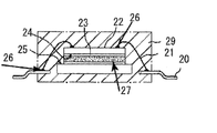
- FIG. 2 shows a schematic diagram of the IGBT.
- a die-bonding electrode portion is provided on the copper base heat sink 25, and a solder layer 27 is further provided thereon.
- the solder layer 27 is further connected to the IC chip 22 through a plating layer 24 formed on the IC chip 22 placed thereon.
- a Cu clip 21 is wired from the electrode formed on the IC chip 22 toward the Cu lead frame 20.
- the IC chip 22 and the Cu clip 21 and the Cu clip 21 and the lead frame 20 are joined by a solder joint 26.
- solder alloy of the present invention for a joint for connecting the emitter and collector of a power device because long-term quality can be maintained even if the current density between terminals is high.
- the solder alloy for power devices of the present invention is not limited to the inside of the power device, but also a joint with a large amount of current between the device and the printed board, such as a joint between the power device and the printed board, or a CPU and a printed board. Even if it is used for a joint having a high current density with the substrate, it is possible to prevent electromigration generated in lands such as Cu and Ni.
- the same reflow profile as that of Sn-3.0Ag-0.5Cu that is generally used may be used.
- the solder alloy for a power device of the present invention can be used for a power device having a solder joint in which a current having a current density of 5 to 100 kA / cm 2 flows. Furthermore, it can be used for mounting on a printed circuit board of a power device constituting a joint through which a current having a current density of 5 to 100 kA / cm 2 flows.
- the solder alloy for a power device of the present invention has excellent heat resistance that can be guaranteed until the temperature inside the electronic device is around 150 ° C. when assembled as a device.
- power devices handle large currents of 1A or more, if the solidus temperature of the solder alloy falls too much, the solder joint becomes semi-molten and the movement of metal atoms cannot be controlled. End up.
- Bi in the solder joint portion of the present invention having a high current density
- Bi when the Bi content exceeds 4%, Bi segregates in the entire solder fillet, and when the current density of the portion where Bi segregates increases, Bi itself is about Sn. Since it has an electric resistance value of 5 times or more, the heat generation is further intense, and the thermal conductivity is very poor, about 1/7 of Sn and 1/40 of Cu. Heating is accelerated. In the remelted portion, Cu diffusion becomes more intense, and electromigration proceeds locally, shortening the life until disconnection.
- the reaction layer with Cu wiring changes from Cu6Sn5 to Cu6 (SnIn) 5, further dissolves in the Sn matrix, distorts the crystal lattice, suppresses Cu diffusion, and has electromigration resistance. Improved.
- the solidus temperature decreases.
- solid solution hardening with In cannot be expected at high temperatures such as 125 ° C.
- In atoms distort the crystal lattice of the Sn matrix. This makes it impossible to resist, accelerates interdiffusion in the Sn matrix due to lowering of the melting point, and lowers electromigration resistance.
- the amount of In added is 5% or less. If possible, 4% or less is good. However, when the amount of In added is less than 2%, the In concentration in the reaction layer with the Cu electrode is lowered, and electromigration occurs frequently.
- the solder alloy for power devices of the present invention has a heat resistance of around 150 ° C. even when used for a joint for connection inside a power device, regardless of the composition of so-called low-temperature solder containing Bi and In, and 5 to 100 kA It is not damaged by electromigration even at high current densities of / cm 2 . Therefore, the power device made of the solder alloy of the present invention can be stably operated for a long time.
- solder alloy of the present invention when used for a wiring joint between a power device and a printed circuit board by mounting a printed circuit board, a fine wiring CPU or the like and a wiring joint between the printed circuit board, etc., 5 to 100 kA / cm Even in a joint that generates a high current density of 2 , electromigration does not occur, so that stable quality over a long period of time can be obtained.
- FIG. 1A and FIG. 1B are schematic diagrams showing Sn lattice models of the conventional example and the example of the present invention, respectively. It is the schematic of IGBT (insulated gate bipolar transistor). It is explanatory drawing which shows the mode of the solder joint of this invention Example. It is an electron micrograph which shows the state of the copper land before supplying the electric current of an Example of this invention. It is an electron micrograph which shows the state of the copper land which resistance value rose 5% after 125 degreeC and 20 ampere current supply of the Example of this invention. It is an electron micrograph which shows the state of the copper land which resistance value rose by 10% after 125 degreeC and 20 ampere current supply of the Example of this invention.
- IGBT insulated gate bipolar transistor
- the present invention is an alloy consisting essentially of 2-4 mass% Ag, 2-4 mass% Bi, 2-5 mass% In and the balance Sn. Ag: It may be 3.2% or less. In: It may be 4.5% or less.
- the alloy may further preferably contain at least one of 0.05 to 0.2% by weight of Ni, 0.05 to 0.2% by weight of Co, and 0.02 to 0.1% of Fe.
- the solder joint according to the present invention can be formed of an alloy consisting essentially of 2 to 4% by mass of Ag, 2 to 4% by mass of Bi, 2 to 5% by mass of In and the balance Sn.
- the alloy constituting the joint may preferably further contain at least one of 0.05 to 0.2% by mass of Ni, 0.05 to 0.2% by mass of Co, and 0.02 to 0.1% of Fe.
- the solder joint according to the present invention is not limited to being used for a specific electronic device, but is particularly effective when used for an electronic device that consumes a large amount of power such as a power transistor. .
- solder joint according to the present invention can be formed in various shapes.
- a method such as flip chip mounting by reflow soldering using wire bonding, preform, solder ball, or solder paste can be considered.
- the mounting on the power device and the printed circuit board or the mounting on the CPU or the printed circuit board may be formed by joining the lead or electrode of the electronic element by jet soldering.
- solder paste, solder balls, or various preforms may be formed by reflow soldering.
- the solder joint according to the present invention may be formed by manual (manual) soldering. These are determined depending on whether the power device is a discrete type or a surface mount type.
- the reason for limiting the range of each composition component in the above alloy is as follows. Improvement of electromigration in SnAgBiIn alloy
- the amount of Ag is determined from the viewpoint of solder melting temperature and thermal fatigue resistance. If the Ag content is less than 2%, the thermal fatigue properties are degraded. On the other hand, if it exceeds 4%, the liquidus increases, so the number of voids increases and the quality of the solder joint deteriorates. Therefore, the Ag content of the present invention is 2% by mass or more and 4% by mass or less.
- the amount of Ag added in the present invention when bumps are formed using solder balls, a coarse Ag3Sn compound that is as large as the diameter of the solder balls crystallizes out during soldering. The compound crystallizes out and causes soldering failure. Therefore, when the amount of Ag added in the present invention is increased, the crystallization of coarse Ag3Sn becomes noticeable by slow cooling, and in order to avoid this, the amount of Ag is further preferably 3.5% or less, and the crystallization of primary crystals is improved. In order to reduce and improve the reliability of solder joints, the Ag content should be 2.5% or more. Therefore, a more preferable amount of Ag is 2.5% by mass or more and 3.5% by mass or less.
- Bi forms a solid solution with Sn matrix and suppresses Cu diffusion in the Sn matrix.
- Bi dissolved in the Sn matrix gives lattice distortion and suppresses diffusion of Cu atoms in the matrix. Electromigration tends to occur at high temperatures of about 150 ° C. Therefore, it is important to maintain the state of solid solution hardening caused by the addition of Bi at such a high temperature. Generally, the state of solid solution hardening disappears when the solder joint is heated to a high temperature of 150 ° C. Furthermore, at 150 ° C, the solid solubility limit of Bi in Sn becomes 10% or more. It is thought that the diffusion of Bi atoms in the Sn matrix becomes intense and the Sn lattice strain is relaxed.
- the Bi addition amount is 4% or less.
- the addition amount of Bi of the present invention is 2% by mass or more and 4% by mass or less.
- Bi crystallizes over the entire fillet portion of the solder joint due to solidification segregation.
- Bi crystallizes in a size of about 10 microns and is dispersed throughout, but the Bi-enriched area has not yet penetrated the entire fillet.
- the segregated area of Bi penetrates the fillet portion.
- the solder joint is rapidly exposed to a high temperature of 150 ° C, the liquid phase part penetrates the fillet part, so even if it suppresses the diffusion of Cu atoms and prevents electromigration, thermal fatigue Properties are significantly reduced. Therefore, such a high Bi content is not suitable for solder joints that require high reliability even when a large current flows.
- the amount of Bi added is limited to 4% or less, preferably 3% or less.
- Bi content is 3% or less, Bi segregation is confirmed at several locations of the fillet, and even if the Bi segregated portion is remelted at 139 ° C., the progress of cracks can be prevented.
- the addition of In does not change the tendency of Se segregation.
- In like Bi, forms a solid solution with Sn and gives lattice distortion to the Sn matrix. Solid solution hardening by addition of In is maintained even at a high temperature of 160 ° C. Although the effect is small compared to Bi, In can also suppress Cu diffusion in the Sn matrix.
- the primary crystal is not ⁇ -Sn but ⁇ -SnIn, and the crystallized ⁇ -SnIn phase becomes a ⁇ -Sn phase by solid phase transformation at 100 ° C or less.
- the crystal grains are refined, the size is 50 ⁇ m or less, and the crystal orientation is random.
- the diffusion rate of Cu atoms in the c-axis direction is fast.
- the crystal grains are large and the probability is high, the distance that Cu atoms can diffuse becomes longer, the amount of Cu that diffuses from the Cu electrode into the solder increases, and the disconnection of the Cu electrode due to electromigration is very short. happenss easily. However, if the crystal grains are small, even if the c-axis and current orientation of some crystal grains coincide, the crystal grains themselves are small, and the total amount of Cu that moves from the Cu electrode into the solder is suppressed, and as a result The life until the conductive path is broken by electromigration is prolonged.
- the amount of In added is less than 2%, the primary crystal is formed and the ⁇ -SnIn phase is hardly crystallized.
- the ⁇ -Sn phase crystallizes from the initial stage of solidification and grows continuously. Therefore, no phase transformation occurs due to the solid phase reaction, and the direction of the current coincides with the C-axis direction of the coarse ⁇ -Sn crystal. Therefore, in the solder joint, the diffusion of Cu atoms becomes intense, and disconnection occurs in a short time.
- In is added in excess of 5%, a ⁇ -Sn phase is formed at room temperature, but at 150 ° C., the ratio of ⁇ -Sn phase to ⁇ -SnIn is about 7: 3.
- the In amount of the present invention is 2% by mass or more and 5% by mass or less. Preferably, it is 3 mass% or more and 4 mass% or less.
- Electromigration can be suppressed directly by adding In.
- intermetallic compounds such as Cu6Sn5 and Cu3Sn are formed at the interface between the Cu electrode and the solder alloy, but the movement of Cu atoms in these intermetallic compound phases (hereinafter also referred to as “reaction phase”)
- reaction phase the movement of Cu atoms in these intermetallic compound phases
- the In content is 1% or more, preferably 2% or more.
- the In content in the reaction phase with the Cu electrode is 7% or less.
- the In content in the Cu6 (SnIn) 5 reaction phase is preferably 7% or less.
- Ni Addition of 0.01-0.3% also has the effect of suppressing electromigration.
- the reaction phase can be changed from Cu6 (SnIn) 5 to (CuNi) 6 (SnIn) 5, and Cu diffusion can be suppressed.
- the amount of Ni added is less than 0.01%, the Cu6 (SnIn) 5 reaction phase may remain unchanged.
- the amount of Ni added is preferably 0.1% or more.
- the temperature is 240 ° C. or lower.
- Ni3 (SnIn) 4 remains at 240 ° C, but has little effect on soldering.
- the Ni content exceeds 0.3%, if it exceeds 0.2% in some cases, adverse effects occur, for example, the amount of voids increases.
- Ni3 (SnIn) 4 remains, the dissolution of Cu into the solder during reflow can be effectively prevented, and as a result, the occurrence of disconnection can be prevented and the service life can be extended.
- a suitable Ni addition amount is 0.01 to 0.2%, and more preferably 0.1 to 0.15%.
- Co Addition of 0.01 to 0.3% has the effect of suppressing electromigration.
- the reaction phase can be changed from Cu6 (SnIn) 5 to (CuCo) 6 (SnIn) 5, and Cu diffusion can be suppressed.
- the Co addition amount is not less than 0.01%, and if it is less than 0.02% in some cases, a part of the Cu6 (SnIn) 5 reaction phase may remain unchanged.
- the amount of Co added is preferably 0.1% or more.
- the heating temperature during reflow should not exceed 260 ° C. Usually, the temperature is 240 ° C. or lower.
- the liquidus exceeds 240 ° C.
- a small amount of Co (SnIn) 2 remains at 240 ° C, but has little effect on soldering. However, if the Co content exceeds 0.3%, in particular, if it exceeds 0.2%, adverse effects occur, for example, the amount of voids increases.
- a suitable Co addition amount is 0.05 to 0.2%, and more preferably 0.05 to 0.15%.
- the reaction phase (CuCo) 6 (SnIn) 5 becomes a smooth surface, a reaction layer is formed, and the thickness becomes uniform.
- Co is added in an amount of less than 0.01%, the unevenness of the reaction phase (CuCo) 6 (SnIn) 5 becomes severe, and when the current is concentrated in a thin portion of the reaction layer, the reaction phase is likely to disappear due to electromigration. After the reaction phase disappears, the Cu electrode and the solder are in direct contact with each other, Cu diffusion from the Cu electrode to the solder is further accelerated, and the wire breaks in a short period of time.
- the ⁇ -Sn crystal grains in the vicinity of the reaction phase can be refined to 30 ⁇ m or less, so that the service life until breakage due to electromigration can be extended.
- a small amount of Fe may be added to the Sn—Ag—Bi—In alloy of the present invention.
- the Fe content is 0.01 to 0.1% when added.
- Remainder Sn substantially constitutes the remainder of the solder alloy.
- the lower limit of the Sn content is not particularly specified, but is generally at least 94% by mass.
- the solder alloy used for the solder joint according to the present invention can be manufactured by a usual method for producing a solder alloy, and the solder alloy at that time is suitable for each soldering method used for forming the solder joint. Can be shaped into a shape.
- the solder alloy according to the present invention may be used in the form of an ingot, bar, rod, solder ball, solder powder, or solder wire, or processed into various preforms such as pellets and disks. May be used.
- solder alloy powder When using a solder alloy as the solder paste, the solder alloy powder is appropriately mixed with the flux by conventional means.
- solder joint of the present invention and the conventional solder joint are made by soldering a Cu element and a land by a reflow method using a solder paste, Various characteristics of the solder joint at that time were measured. Solder powder having each solder alloy component shown in Table 1 was mixed with flux to form a solder paste.
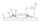
- the solder paste is printed on the copper electrode of the circuit board 31 by, for example, a stencil, and then a rectangular Cu plate 33 is placed on the solder paste.
- the circuit board 31 and the copper plate 33 are heated in a reflow furnace, the solder paste is melted, and then the assembly at this time is cooled, and the solder joint 34 for joining the Cu plate 33 and the land 32 of the circuit board 31 to each other.
- FIG. 3 schematically shows the state of the circuit board 1 at this time.
- the heat cycle property test was conducted as follows. A 6-layer FR4 printed circuit board with a thickness of 1.6 mm was used. A soldering pattern (1.6 ⁇ 1.2 (mm)) of a predetermined solder paste was printed in a thickness of 150 ⁇ m with the same opening size as the substrate electrode size. After mounting 3.2mm ⁇ 1.6mm ⁇ 0.6mm size ceramic chip resistor parts on SMT-2000V SUZUKI) automatic component mounting machine, using Senju Metal SNR-825, peak temperature 240 ° C, oxygen Mounting was performed at a concentration of 500 ppm or less.
- the minimum joint strength of 3216 parts is 15N
- the cumulative frequency that is 15N or less is calculated every 500 cycles, and it is rejected when the cumulative frequency exceeds 10%
- the life before 500 cycles was defined as the life of the solder joint. The results are listed in Table 1.
- the electromigration test was conducted as follows. When obtaining resistance to electromigration, the copper plate 33 and the land 32 of the circuit board 31 are appropriately connected to a power source 35 as shown in FIG. 3, and between the Cu plate 33 and the land 32 of the circuit board 31. Apply current. The current at this time is supplied until the resistance increases to 5% and 10% while the circuit board 31 is kept in the atmosphere at room temperature. At the end, the cross section of the solder joint 34 near the bottom of the fillet portion of the solder joint 34 is observed with an electron microscope. The area of the fillet portion is observed because this is where the current density seems to be the highest.
- FIG. 4 is an electron micrograph showing the state of the copper land before applying the current of the embodiment of the present invention.
- FIG. 5 is an electron micrograph showing the state of a copper land having a resistance value increased by 5% after applying a current of 125 ° C. and 20 A according to the embodiment of the present invention.
- FIG. 6 is an electron micrograph showing the state of a copper land having a resistance value increased by 10% after energization at 125 ° C. and 20 A according to the embodiment of the present invention.
- the Cu land of the circuit board was considerably thin due to electromigration as compared to FIG. 4 before the energization test.
- 5 and 6 that the solder joint is broken at a part of the joint shown as a black region. In this region, there is no longer any connection between the solder joint and the Cu land of the circuit board.
- the SnAgBiIn alloy used in the solder joint according to the present invention has much better fatigue resistance than either the SnAgCu alloy or the SnCu alloy. From the experimental results described above, it can be seen that the solder joint according to the present invention is substantially free from electromigration even when used for a long time at a current density in the range of 5 to 100 kA / cm 2 . At the same time, they are excellent in heat cycle resistance and fatigue resistance. Therefore, the solder joint according to the present invention is particularly suitable for use in electronic devices that operate with a large current having a high current density, such as power transistors and other power devices.
Abstract
Description
なお、本明細書において、はんだ合金組成を規定する説明において単に「%」とあるのは「質量%」の意味である。
第1の方法は、Snのマトリックスで形成させるはんだ合金内部のCu原子の拡散を抑制して、急激に電流が流れないようにする方法で、エレクトロマイグレーション防止にとても有効である。
また、本発明のパワーデバイス用のはんだ合金は、パワーデバイス内部だけではなく、パワーデバイスとプリント基板との継手などのように、デバイスとプリント基板の間の電流量が多い継手や、CPUとプリント基板との間の電流密度が高い部分の継手に使用しても、CuやNi等のランドに発生するエレクトロマイグレーションを防止することができる。この電子デバイスとプリント基板との接合では、一般に使用されるSn-3.0Ag-0.5Cuと同じリフロープロファイルで使用して良い。
凝固偏析でBi単相がはんだフィレット全体に晶出するため、はんだ接合部で局所的に電流密度が高くなるとはんだ自体がジュール熱で発熱し、瞬間的に150℃を超過し、一部溶解する。通常のヒートサイクル試験や従来のように、ピッチが広く電流量が小さいパワーサイクル試験ではジュール熱が発生しても、熱拡散により局所的にはんだフィレットの一部の温度が上昇することはなく、平均的に温度が上昇するため、大きな問題とはならず、更に、昇温がゆっくりと行われるため、Bi単相がSnマトリックスに再固溶し、低融点層が消失し、Biの偏析による再溶融の懸念はない。
In添加によりCu配線との反応層がCu6Sn5からCu6(SnIn)5への変化し、更に、Snマトリックス中に固溶し、結晶格子を歪ませ、Cuの拡散を抑制し、耐エレクトロマイグレーション性が改善される。一方で、Inの添加量が増加すると固相線温度が低下し、特に、125℃のような高温下ではInによる固溶硬化は期待できず、つまり、In原子がSnマトリックスの結晶格子を歪ませることができなくなり、融点低下によるSnマトリックス中の相互拡散を加速させ、耐エレクトロマイグレーション性を低下させる。更に、125℃の高温下ではβ-Sn相の一部がγ-SnIn相に変態し、Sn,In原子の拡散が激しくなるとともに原子空孔が多く形成される。原子空孔を介してCuが更に拡散しやすくなるため、高温でのγ-SnIn相への変態は極力避けなければならない。そのため、In添加量は5%以下とする。できれば、4%以下がよい。しかしながら、In添加量を2%未満にするとCu電極との反応層中のIn濃度が低下し、エレクトロマイグレーションが多く発生するようになる。
上記合金は、好ましくは、さらに、0.05~0.2質量%のNi、0.05~0.2質量%のCo、および0.02~0.1%のFeの少なくとも1種を含有してもよい。
上記継手を構成する合金は、好ましくは、さらに、0.05~0.2質量%のNi、0.05~0.2質量%のCo、および0.02~0.1%のFeの少なくとも1種を含有してもよい。
SnAgBiIn合金でのエレクトロマイグレーションの改善について
Ag量は、はんだの溶融温度、耐熱疲労特性の観点から決定される。
Agが2%より少ないと熱疲労特性が低下する。一方、4%を超過すると液相線が上昇するため、ボイドの数が増加し、はんだ継手の品質が低下する。したがって本発明のAg量は、2質量%以上、4質量%以下である。
エレクトロマイグレーションは150℃程度の高温下では発生しやすい。したがって、そのような高温下でBi添加により起こる固溶硬化の状態を維持することが重要である。一般的に、固溶硬化の状態は、150℃という高温にはんだ継手が加熱されると、消失し、更に、150℃ではSnへのBiの固溶限が10%以上になるので、BiではSnマトリックス中のBi原子の拡散が激しくなり、Sn格子ひずみが緩和されると考えられる。Biを2%以上添加した場合、150℃以上の高温化においても固溶硬化が持続することが判明しており、固溶硬化が持続することで発生するSnの格子歪みの存在は、Cu原子の拡散を抑制する。160℃での引張強度はSnAg0.5Cu、Sn3Ag0.8Cu3Biで各々、19MPaと28MPaであり、200℃でも13MPaと20MPaである。Biが2質量%未満では、固溶硬化が発揮されず、Snの格子歪みが現れない。しかしながら、過剰にBiを添加すると、前述の固相線温度の低下の観点以外にもはんだ付け時の凝固偏析により、139℃で溶融する低融点相(低温相)が晶出する。はんだ継手におけるそのような低温相の存在により、はんだ継手は150℃以上という高温に加熱されることがあることから、そのときに液相の生成はさけられない。そのため、熱疲労による応力負荷の増大により、クラックが一気に進展する。そのため、Bi添加量は4%以下とする。本発明のBiの添加量は、2質量%以上、4質量%以下である。
一方で、5%を超過してInを添加すると、室温ではβ-Sn相が生成するが、150℃ではβ-Sn相とγ-SnInの割合が約7:3となる。このことは、はんだ継手が使用中に相変態を起こすことを意味する。もし、そのようなβ-Snから、β-Snとγ-SnInへの相変態が起こると、はんだ継手が変形し、隣接する電極との短絡が起こる。そのため、In含量は5%以下に限定する。本発明のIn量は、2質量%以上、5質量%以下である。好ましくは、3質量以上、4質量%以下である。
本発明のSn-Ag-Bi-In合金には少量のFeを配合させても良い。好ましくは、Fe含量は、添加する場合、0.01~0.1%とする。
Snは当該はんだ合金の残部を実質上構成する。Sn含量の下限は、特に規定しないが、一般には、少なくとも94質量%である。
厚さが1.6mmで6層のFR4プリント基板を使用した。基板電極サイズと同じ開口サイズで150μm厚に所定のソルダペーストをはんだ付けパターン(1.6×1.2(mm))を印刷した。これに、3.2mm×1.6mm×0.6mmサイズのセラミックスチップ抵抗分品をSMT-2000V SUZUKI)製の自動部品搭載機で搭載後、千住金属製SNR-825を使って、ピーク温度240℃、酸素濃度500ppm以下で実装を行った。
エレクトロマイグレーションに対する抵抗性を求める場合、銅プレート33および回路基板31のランド32とを図3に示すように、適宜電源35に接続して、Cuプレート33と回路基板31のランド32との間に電流を流す。このときの電流は、回路基板31を室温の大気下に保持したまま、抵抗が5%、10%まで増加するまで供給する。終了時、はんだ継手34のフィレット部の底部近くのはんだ継手34の断面を電子顕微鏡で観察する。フィレット部の領域を観察するのは、そこが、電流密度が最も高いと思われる個所であるからである。
最後に、リフローのピーク温度を240℃で設定したリフロー炉で、はんだ付け後の回路基板1をX線透過装置によってはんだフィレットを確認して、はんだ継手のボイドを調べた。継手断面の面積比でボイドが20%以上のものを「×」、10~20%のものを「△」、10%未満のものを「○」と判定した。結果は、表1に示す。

図5は、本発明実施例の125℃、20 A通電後に、抵抗値が5%上昇した銅ランドの状態を示す電子顕微鏡写真である。
図5、図6は、通電試験前の図4と比較すると、エレクトロマイグレーションにより、回路基板のCuランドがかなり薄くなっていた。そして、図5および図6からは、はんだ継手において、黒い領域として示される継手の一部で破断が起こっていることがわかる。この領域では、はんだ継手と、回路基板のCuランドとの間は、もはや接続されていない。
以上説明した実験結果から、本発明にかかるはんだ継手は、5~100 kA/cm2の範囲の電流密度で長期間使用しても、エレクトロマイグレーションは実質上起こらないことが分かる。そして同時に、それらは、耐ヒートサイクル性、そして耐疲労性に優れている。したがって、本発明にかかるはんだ継手は、電流密度が高い大きな電流で動作する電子機器、例えばパワートランジスタおよびその他の電力機器などに用いるに特に適する。
Claims (6)
- 5~100 kA/cm2の電流密度の電流が流れる継手を有する電子デバイス用のはんだ合金であって、2~4質量%のAg,2~4質量%のBi,2~5質量%のIn、残部Snから本質的に構成されるはんだ合金。
- 2.5~3.5質量%のAg,2~3質量%のBi,3~4質量%のIn、残部Snから本質的に構成される請求項1に記載のはんだ合金。
- さらに、0.01~0.3質量%のNi、および0.01~0.32質量%のCo、0.01~0.1質量%のFeから選択された1種以上を含有する請求項1または2に記載のはんだ合金。
- 2~4質量%のAg,2~4質量%のBi,2~5質量%のIn、残部Snから本質的になるはんだ合金から作られたはんだ継手であって、電子デバイス内部のはんだ継手、または電子デバイスに接続されたはんだ継手であり、当該はんだ継手の少なくとも一部に5~100 kA/cm2の電流密度の電流が流れることを特徴とするはんだ継手。
- 前記はんだ継手は、2~4質量%のAg,2~4質量%のBi,2~5質量%のIn、残部Snから本質的になるはんだ合金に、さらに0.01~0.3質量%のNi、0.01~0.32質量%のCo、および0.01~0.1質量%のFeの少なくとも一種を含有するはんだ合金から作られた請求項4記載のはんだ継手。
- デバイス内部に、2~4質量%のAg,2~4質量%のBi,2~5質量%のIn、残部Snから本質的になるはんだ合金から作られたはんだ継手を有し、継手の少なくとも一部に5~100 kA/cm2の電流密度が流れることを特徴とするパワーデバイス。
Priority Applications (10)
| Application Number | Priority Date | Filing Date | Title |
|---|---|---|---|
| KR1020167022266A KR101752616B1 (ko) | 2011-02-25 | 2012-02-27 | 파워 디바이스용의 땜납 합금과 고전류 밀도의 땜납 조인트 |
| JP2013501162A JP5418718B2 (ja) | 2011-02-25 | 2012-02-27 | パワーデバイス用のはんだ合金と高電流密度のはんだ継手 |
| ES12749274T ES2799421T3 (es) | 2011-02-25 | 2012-02-27 | Uso de una aleación de soldadura y una unión soldada de alta densidad de corriente |
| BR112013021668-9A BR112013021668B1 (pt) | 2011-02-25 | 2012-02-27 | Liga de solda para um dispositivo eletrônico, junta de solda e dispositivo de energia |
| KR1020137024708A KR20130118993A (ko) | 2011-02-25 | 2012-02-27 | 파워 디바이스용의 땜납 합금과 고전류 밀도의 땜납 조인트 |
| CN201280020363.0A CN103501959B (zh) | 2011-02-25 | 2012-02-27 | 功率器件用的焊料合金和高电流密度的焊料接头 |
| KR1020167017967A KR101773733B1 (ko) | 2011-02-25 | 2012-02-27 | 파워 디바이스용의 땜납 합금과 고전류 밀도의 땜납 조인트 |
| EP12749274.2A EP2679334B1 (en) | 2011-02-25 | 2012-02-27 | Use of a solder alloy and soldered joint of high current density |
| US14/001,561 US20140112710A1 (en) | 2011-02-25 | 2012-02-27 | Solder Alloy for Power Devices and Solder Joint Having a High Current Density |
| US17/010,990 US11331759B2 (en) | 2011-02-25 | 2020-09-03 | Solder alloy for power devices and solder joint having a high current density |
Applications Claiming Priority (2)
| Application Number | Priority Date | Filing Date | Title |
|---|---|---|---|
| JP2011-057183 | 2011-02-25 | ||
| JP2011057183 | 2011-02-25 |
Related Child Applications (2)
| Application Number | Title | Priority Date | Filing Date |
|---|---|---|---|
| US14/001,561 A-371-Of-International US20140112710A1 (en) | 2011-02-25 | 2012-02-27 | Solder Alloy for Power Devices and Solder Joint Having a High Current Density |
| US17/010,990 Division US11331759B2 (en) | 2011-02-25 | 2020-09-03 | Solder alloy for power devices and solder joint having a high current density |
Publications (1)
| Publication Number | Publication Date |
|---|---|
| WO2012115268A1 true WO2012115268A1 (ja) | 2012-08-30 |
Family
ID=46721035
Family Applications (1)
| Application Number | Title | Priority Date | Filing Date |
|---|---|---|---|
| PCT/JP2012/054774 WO2012115268A1 (ja) | 2011-02-25 | 2012-02-27 | パワーデバイス用のはんだ合金と高電流密度のはんだ継手 |
Country Status (10)
| Country | Link |
|---|---|
| US (2) | US20140112710A1 (ja) |
| EP (1) | EP2679334B1 (ja) |
| JP (1) | JP5418718B2 (ja) |
| KR (3) | KR20130118993A (ja) |
| CN (1) | CN103501959B (ja) |
| BR (1) | BR112013021668B1 (ja) |
| ES (1) | ES2799421T3 (ja) |
| MY (1) | MY157295A (ja) |
| TW (1) | TWI565550B (ja) |
| WO (1) | WO2012115268A1 (ja) |
Cited By (9)
| Publication number | Priority date | Publication date | Assignee | Title |
|---|---|---|---|---|
| EP2671667A1 (en) * | 2012-06-08 | 2013-12-11 | Nihon Almit Co., Ltd. | Solder paste for bonding micro components |
| WO2014129258A1 (ja) * | 2013-02-25 | 2014-08-28 | ソニー株式会社 | 半田組成物、電気接続構造、電気接続部材、プリント配線板および電子回路装置 |
| JP5590272B1 (ja) * | 2012-12-18 | 2014-09-17 | 千住金属工業株式会社 | 鉛フリーはんだ合金 |
| JP5638174B1 (ja) * | 2014-06-24 | 2014-12-10 | ハリマ化成株式会社 | はんだ合金、はんだ組成物、ソルダペーストおよび電子回路基板 |
| WO2016084550A1 (ja) * | 2014-11-27 | 2016-06-02 | 新日鉄住金マテリアルズ株式会社 | 無鉛はんだバンプ接合構造 |
| WO2018159664A1 (ja) * | 2017-02-28 | 2018-09-07 | 千住金属工業株式会社 | はんだ材料、はんだペースト、フォームはんだ及びはんだ継手 |
| JPWO2017134974A1 (ja) * | 2016-02-01 | 2018-10-04 | 株式会社村田製作所 | 接合材、それを用いた接合方法及び接合構造 |
| JP2020192552A (ja) * | 2019-05-27 | 2020-12-03 | 千住金属工業株式会社 | はんだ合金、はんだペースト、プリフォームはんだ、はんだボール、線はんだ、脂入りはんだ、はんだ継手、電子回路基板および多層電子回路基板 |
| WO2024048371A1 (ja) * | 2022-09-02 | 2024-03-07 | 株式会社デンソー | 半導体装置 |
Families Citing this family (4)
| Publication number | Priority date | Publication date | Assignee | Title |
|---|---|---|---|---|
| JP6365653B2 (ja) * | 2016-08-19 | 2018-08-01 | 千住金属工業株式会社 | はんだ合金、はんだ継手およびはんだ付け方法 |
| WO2020241437A1 (ja) | 2019-05-27 | 2020-12-03 | 千住金属工業株式会社 | はんだ合金、ソルダペースト、はんだボール、ソルダプリフォーム、はんだ継手、車載電子回路、ecu電子回路、車載電子回路装置、およびecu電子回路装置 |
| CN112317972B (zh) * | 2020-09-30 | 2021-07-20 | 厦门大学 | 一种单向性耐高温焊接接头的低温快速制造方法 |
| KR102394475B1 (ko) | 2021-09-14 | 2022-05-04 | 마이크로컴퍼지트 주식회사 | 저융점 고신뢰성 솔더 입자, 이를 포함하는 수지 조성물 |
Citations (8)
| Publication number | Priority date | Publication date | Assignee | Title |
|---|---|---|---|---|
| JPH08206874A (ja) | 1995-02-06 | 1996-08-13 | Matsushita Electric Ind Co Ltd | はんだ材料 |
| JPH0970687A (ja) | 1995-07-04 | 1997-03-18 | Toyota Central Res & Dev Lab Inc | 無鉛はんだ合金 |
| JPH1071488A (ja) * | 1996-08-29 | 1998-03-17 | Mitsui Mining & Smelting Co Ltd | 錫−銀系半田合金 |
| WO2000018536A1 (fr) * | 1998-09-30 | 2000-04-06 | Matsushita Electric Industrial Co., Ltd. | Materiau de brasage et dispositif electrique/electronique utilisant celui-ci |
| JP2001071174A (ja) * | 1999-09-07 | 2001-03-21 | Mitsui Mining & Smelting Co Ltd | 錫−銀系ハンダ合金 |
| JP2002096191A (ja) * | 2000-09-18 | 2002-04-02 | Matsushita Electric Ind Co Ltd | はんだ材料およびこれを利用する電気・電子機器 |
| JP2005072173A (ja) | 2003-08-22 | 2005-03-17 | Senju Metal Ind Co Ltd | 電子部品およびソルダペースト |
| JP2010123873A (ja) * | 2008-11-21 | 2010-06-03 | Sanyo Electric Co Ltd | 絶縁ゲート型半導体装置 |
Family Cites Families (10)
| Publication number | Priority date | Publication date | Assignee | Title |
|---|---|---|---|---|
| JP2805595B2 (ja) * | 1994-11-02 | 1998-09-30 | 三井金属鉱業株式会社 | 鉛無含有半田合金 |
| JP2000173253A (ja) * | 1998-09-30 | 2000-06-23 | Matsushita Electric Ind Co Ltd | 携帯所持可能なミニディスクプレイヤ― |
| US20010036420A1 (en) * | 1999-09-07 | 2001-11-01 | Mitsui Mining & Smelting Company, Ltd. | Tin-silver based soldering alloy utility |
| KR100398716B1 (ko) * | 2000-06-12 | 2003-09-19 | 가부시키가이샤 히타치세이사쿠쇼 | 반도체 모듈 및 반도체 장치를 접속한 회로 기판 |
| US8216395B2 (en) * | 2001-06-28 | 2012-07-10 | Senju Metal Industry Co., Ltd. | Lead-free solder alloy |
| US6822327B1 (en) * | 2003-06-13 | 2004-11-23 | Delphi Technologies, Inc. | Flip-chip interconnected with increased current-carrying capability |
| EP2177305B1 (en) | 2007-07-18 | 2013-07-03 | Senju Metal Industry Co., Ltd | In-containing lead-free solder for on-vehicle electronic circuit |
| US8598464B2 (en) | 2009-04-20 | 2013-12-03 | Panasonic Corporation | Soldering material and electronic component assembly |
| CN201515304U (zh) * | 2009-08-19 | 2010-06-23 | 长春思达汽车技术咨询有限公司 | 电动汽车电池分组交替回馈储能装置 |
| CN102700428B (zh) * | 2012-06-12 | 2015-06-10 | 福建省福工动力技术有限公司 | 带锂电池和超级电容的电动汽车控制系统及其控制方法 |
-
2012
- 2012-02-27 KR KR1020137024708A patent/KR20130118993A/ko active Application Filing
- 2012-02-27 EP EP12749274.2A patent/EP2679334B1/en active Active
- 2012-02-27 CN CN201280020363.0A patent/CN103501959B/zh active Active
- 2012-02-27 KR KR1020167017967A patent/KR101773733B1/ko active IP Right Grant
- 2012-02-27 BR BR112013021668-9A patent/BR112013021668B1/pt active IP Right Grant
- 2012-02-27 MY MYPI2013701489A patent/MY157295A/en unknown
- 2012-02-27 WO PCT/JP2012/054774 patent/WO2012115268A1/ja active Application Filing
- 2012-02-27 JP JP2013501162A patent/JP5418718B2/ja active Active
- 2012-02-27 ES ES12749274T patent/ES2799421T3/es active Active
- 2012-02-27 US US14/001,561 patent/US20140112710A1/en not_active Abandoned
- 2012-02-27 KR KR1020167022266A patent/KR101752616B1/ko active IP Right Grant
- 2012-02-29 TW TW101106527A patent/TWI565550B/zh active
-
2020
- 2020-09-03 US US17/010,990 patent/US11331759B2/en active Active
Patent Citations (8)
| Publication number | Priority date | Publication date | Assignee | Title |
|---|---|---|---|---|
| JPH08206874A (ja) | 1995-02-06 | 1996-08-13 | Matsushita Electric Ind Co Ltd | はんだ材料 |
| JPH0970687A (ja) | 1995-07-04 | 1997-03-18 | Toyota Central Res & Dev Lab Inc | 無鉛はんだ合金 |
| JPH1071488A (ja) * | 1996-08-29 | 1998-03-17 | Mitsui Mining & Smelting Co Ltd | 錫−銀系半田合金 |
| WO2000018536A1 (fr) * | 1998-09-30 | 2000-04-06 | Matsushita Electric Industrial Co., Ltd. | Materiau de brasage et dispositif electrique/electronique utilisant celui-ci |
| JP2001071174A (ja) * | 1999-09-07 | 2001-03-21 | Mitsui Mining & Smelting Co Ltd | 錫−銀系ハンダ合金 |
| JP2002096191A (ja) * | 2000-09-18 | 2002-04-02 | Matsushita Electric Ind Co Ltd | はんだ材料およびこれを利用する電気・電子機器 |
| JP2005072173A (ja) | 2003-08-22 | 2005-03-17 | Senju Metal Ind Co Ltd | 電子部品およびソルダペースト |
| JP2010123873A (ja) * | 2008-11-21 | 2010-06-03 | Sanyo Electric Co Ltd | 絶縁ゲート型半導体装置 |
Cited By (17)
| Publication number | Priority date | Publication date | Assignee | Title |
|---|---|---|---|---|
| EP2671667A1 (en) * | 2012-06-08 | 2013-12-11 | Nihon Almit Co., Ltd. | Solder paste for bonding micro components |
| JP5590272B1 (ja) * | 2012-12-18 | 2014-09-17 | 千住金属工業株式会社 | 鉛フリーはんだ合金 |
| EP2937432A4 (en) * | 2012-12-18 | 2016-10-05 | Senju Metal Industry Co | LEAD FREE WELDING ALLOY |
| WO2014129258A1 (ja) * | 2013-02-25 | 2014-08-28 | ソニー株式会社 | 半田組成物、電気接続構造、電気接続部材、プリント配線板および電子回路装置 |
| US9931716B2 (en) | 2014-06-24 | 2018-04-03 | Harima Chemicals, Incorporated | Solder alloy, solder composition, solder paste, and electronic circuit board |
| JP5638174B1 (ja) * | 2014-06-24 | 2014-12-10 | ハリマ化成株式会社 | はんだ合金、はんだ組成物、ソルダペーストおよび電子回路基板 |
| US9956649B2 (en) | 2014-06-24 | 2018-05-01 | Harima Chemicals, Incorporated | Solder alloy, solder paste, and electronic circuit board |
| WO2016084550A1 (ja) * | 2014-11-27 | 2016-06-02 | 新日鉄住金マテリアルズ株式会社 | 無鉛はんだバンプ接合構造 |
| JP2016103530A (ja) * | 2014-11-27 | 2016-06-02 | 新日鉄住金マテリアルズ株式会社 | 無鉛はんだバンプ接合構造 |
| JPWO2017134974A1 (ja) * | 2016-02-01 | 2018-10-04 | 株式会社村田製作所 | 接合材、それを用いた接合方法及び接合構造 |
| WO2018159664A1 (ja) * | 2017-02-28 | 2018-09-07 | 千住金属工業株式会社 | はんだ材料、はんだペースト、フォームはんだ及びはんだ継手 |
| JP2018140427A (ja) * | 2017-02-28 | 2018-09-13 | 千住金属工業株式会社 | はんだ材料、はんだペースト、フォームはんだ及びはんだ継手 |
| JP2020192552A (ja) * | 2019-05-27 | 2020-12-03 | 千住金属工業株式会社 | はんだ合金、はんだペースト、プリフォームはんだ、はんだボール、線はんだ、脂入りはんだ、はんだ継手、電子回路基板および多層電子回路基板 |
| WO2020241225A1 (ja) * | 2019-05-27 | 2020-12-03 | 千住金属工業株式会社 | はんだ合金、はんだペースト、プリフォームはんだ、はんだボール、線はんだ、脂入りはんだ、はんだ継手、電子回路基板および多層電子回路基板 |
| KR20210083367A (ko) * | 2019-05-27 | 2021-07-06 | 센주긴조쿠고교 가부시키가이샤 | 땜납 합금, 땜납 페이스트, 프리폼 땜납, 땜납 볼, 선 땜납, 수지 플럭스 코어드 땜납, 땜납 이음매, 전자 회로 기판 및 다층 전자 회로 기판 |
| KR102342394B1 (ko) | 2019-05-27 | 2021-12-22 | 센주긴조쿠고교 가부시키가이샤 | 땜납 합금, 땜납 페이스트, 프리폼 땜납, 땜납 볼, 선 땜납, 수지 플럭스 코어드 땜납, 땜납 이음매, 전자 회로 기판 및 다층 전자 회로 기판 |
| WO2024048371A1 (ja) * | 2022-09-02 | 2024-03-07 | 株式会社デンソー | 半導体装置 |
Also Published As
| Publication number | Publication date |
|---|---|
| KR20160101209A (ko) | 2016-08-24 |
| EP2679334A4 (en) | 2016-06-01 |
| MY157295A (en) | 2016-05-20 |
| US20210008670A1 (en) | 2021-01-14 |
| ES2799421T3 (es) | 2020-12-17 |
| US11331759B2 (en) | 2022-05-17 |
| TWI565550B (zh) | 2017-01-11 |
| KR101752616B1 (ko) | 2017-06-29 |
| EP2679334A1 (en) | 2014-01-01 |
| JPWO2012115268A1 (ja) | 2014-07-07 |
| US20140112710A1 (en) | 2014-04-24 |
| TW201302366A (zh) | 2013-01-16 |
| KR101773733B1 (ko) | 2017-08-31 |
| KR20130118993A (ko) | 2013-10-30 |
| CN103501959A (zh) | 2014-01-08 |
| EP2679334B1 (en) | 2020-05-27 |
| JP5418718B2 (ja) | 2014-02-19 |
| BR112013021668B1 (pt) | 2019-04-02 |
| KR20160086964A (ko) | 2016-07-20 |
| CN103501959B (zh) | 2016-03-16 |
| BR112013021668A2 (pt) | 2016-11-01 |
Similar Documents
| Publication | Publication Date | Title |
|---|---|---|
| JP5418718B2 (ja) | パワーデバイス用のはんだ合金と高電流密度のはんだ継手 | |
| US11145615B2 (en) | Solder material for semiconductor device | |
| US8888932B2 (en) | Indium-containing lead-free solder for vehicle-mounted electronic circuits | |
| JPWO2018168858A1 (ja) | はんだ材 | |
| JP3892190B2 (ja) | 混載実装構造体及び混載実装方法並びに電子機器 | |
| CN117428367A (zh) | 软钎料合金、焊料球、焊膏和钎焊接头 | |
| JPWO2020158660A1 (ja) | はんだ接合部 | |
| US10189119B2 (en) | Solder alloy for die bonding | |
| JP2018047499A (ja) | Bi基はんだ合金及びその製造方法、並びに、そのはんだ合金を用いた電子部品及び電子部品実装基板 | |
| JP2019155466A (ja) | はんだ合金と車載電子回路 | |
| KR102579479B1 (ko) | 접속핀 | |
| KR102579478B1 (ko) | 전기접속용 금속핀 | |
| JP7291320B2 (ja) | はんだ接合部の製造方法 | |
| JP2016123983A (ja) | 鉛フリーはんだ合金およびそれを用いた半導体装置 | |
| KR20240033889A (ko) | 접속핀 | |
| Geng et al. | New generation of lead-free solder alloys with high thermal reliability for applications in harsh environments |
Legal Events
| Date | Code | Title | Description |
|---|---|---|---|
| WWE | Wipo information: entry into national phase |
Ref document number: 201280020363.0 Country of ref document: CN |
|
| 121 | Ep: the epo has been informed by wipo that ep was designated in this application |
Ref document number: 12749274 Country of ref document: EP Kind code of ref document: A1 |
|
| DPE1 | Request for preliminary examination filed after expiration of 19th month from priority date (pct application filed from 20040101) | ||
| ENP | Entry into the national phase |
Ref document number: 2013501162 Country of ref document: JP Kind code of ref document: A |
|
| WWE | Wipo information: entry into national phase |
Ref document number: 1301004712 Country of ref document: TH |
|
| NENP | Non-entry into the national phase |
Ref country code: DE |
|
| ENP | Entry into the national phase |
Ref document number: 20137024708 Country of ref document: KR Kind code of ref document: A |
|
| WWE | Wipo information: entry into national phase |
Ref document number: 2012749274 Country of ref document: EP |
|
| WWE | Wipo information: entry into national phase |
Ref document number: 14001561 Country of ref document: US |
|
| REG | Reference to national code |
Ref country code: BR Ref legal event code: B01A Ref document number: 112013021668 Country of ref document: BR |
|
| ENP | Entry into the national phase |
Ref document number: 112013021668 Country of ref document: BR Kind code of ref document: A2 Effective date: 20130823 |