WO2012115267A1 - 光電変換素子および光電変換装置 - Google Patents
光電変換素子および光電変換装置 Download PDFInfo
- Publication number
- WO2012115267A1 WO2012115267A1 PCT/JP2012/054771 JP2012054771W WO2012115267A1 WO 2012115267 A1 WO2012115267 A1 WO 2012115267A1 JP 2012054771 W JP2012054771 W JP 2012054771W WO 2012115267 A1 WO2012115267 A1 WO 2012115267A1
- Authority
- WO
- WIPO (PCT)
- Prior art keywords
- layer
- photoelectric conversion
- semiconductor layer
- light absorption
- group
- Prior art date
- Legal status (The legal status is an assumption and is not a legal conclusion. Google has not performed a legal analysis and makes no representation as to the accuracy of the status listed.)
- Ceased
Links
Images








Classifications
-
- H—ELECTRICITY
- H10—SEMICONDUCTOR DEVICES; ELECTRIC SOLID-STATE DEVICES NOT OTHERWISE PROVIDED FOR
- H10F—INORGANIC SEMICONDUCTOR DEVICES SENSITIVE TO INFRARED RADIATION, LIGHT, ELECTROMAGNETIC RADIATION OF SHORTER WAVELENGTH OR CORPUSCULAR RADIATION
- H10F77/00—Constructional details of devices covered by this subclass
- H10F77/20—Electrodes
- H10F77/244—Electrodes made of transparent conductive layers, e.g. transparent conductive oxide [TCO] layers
- H10F77/247—Electrodes made of transparent conductive layers, e.g. transparent conductive oxide [TCO] layers comprising indium tin oxide [ITO]
-
- H—ELECTRICITY
- H10—SEMICONDUCTOR DEVICES; ELECTRIC SOLID-STATE DEVICES NOT OTHERWISE PROVIDED FOR
- H10F—INORGANIC SEMICONDUCTOR DEVICES SENSITIVE TO INFRARED RADIATION, LIGHT, ELECTROMAGNETIC RADIATION OF SHORTER WAVELENGTH OR CORPUSCULAR RADIATION
- H10F10/00—Individual photovoltaic cells, e.g. solar cells
- H10F10/10—Individual photovoltaic cells, e.g. solar cells having potential barriers
- H10F10/16—Photovoltaic cells having only PN heterojunction potential barriers
- H10F10/167—Photovoltaic cells having only PN heterojunction potential barriers comprising Group I-III-VI materials, e.g. CdS/CuInSe2 [CIS] heterojunction photovoltaic cells
-
- H—ELECTRICITY
- H10—SEMICONDUCTOR DEVICES; ELECTRIC SOLID-STATE DEVICES NOT OTHERWISE PROVIDED FOR
- H10F—INORGANIC SEMICONDUCTOR DEVICES SENSITIVE TO INFRARED RADIATION, LIGHT, ELECTROMAGNETIC RADIATION OF SHORTER WAVELENGTH OR CORPUSCULAR RADIATION
- H10F77/00—Constructional details of devices covered by this subclass
- H10F77/10—Semiconductor bodies
- H10F77/14—Shape of semiconductor bodies; Shapes, relative sizes or dispositions of semiconductor regions within semiconductor bodies
- H10F77/147—Shapes of bodies
-
- Y—GENERAL TAGGING OF NEW TECHNOLOGICAL DEVELOPMENTS; GENERAL TAGGING OF CROSS-SECTIONAL TECHNOLOGIES SPANNING OVER SEVERAL SECTIONS OF THE IPC; TECHNICAL SUBJECTS COVERED BY FORMER USPC CROSS-REFERENCE ART COLLECTIONS [XRACs] AND DIGESTS
- Y02—TECHNOLOGIES OR APPLICATIONS FOR MITIGATION OR ADAPTATION AGAINST CLIMATE CHANGE
- Y02E—REDUCTION OF GREENHOUSE GAS [GHG] EMISSIONS, RELATED TO ENERGY GENERATION, TRANSMISSION OR DISTRIBUTION
- Y02E10/00—Energy generation through renewable energy sources
- Y02E10/50—Photovoltaic [PV] energy
- Y02E10/541—CuInSe2 material PV cells
Definitions
- the present invention relates to a photoelectric conversion element and a photoelectric conversion device.
- a photoelectric conversion device used for solar power generation or the like there is one in which a light absorption layer is formed of a chalcopyrite-based I-III-VI group compound semiconductor such as CIGS having a high light absorption coefficient.
- CIGS has a high light absorption coefficient and is suitable for reducing the thickness, area, and cost of photoelectric conversion devices, and research and development of next-generation solar cells using the photoelectric conversion device is being promoted.
- the photoelectric conversion element includes a lower electrode such as a metal electrode on a substrate such as glass, a photoelectric conversion layer that is a semiconductor layer including a light absorption layer and a buffer layer, and an upper electrode such as a transparent electrode and a metal electrode. These are stacked in this order.
- the plurality of photoelectric conversion elements are electrically connected in series by electrically connecting the upper electrode of one adjacent photoelectric conversion element and the lower electrode of the other photoelectric conversion element by a connecting conductor. ing.
- CdS is deposited on a light absorption layer by a chemical deposition method to a thickness of 10 nm to form a buffer layer, and a binary target of a ZnO target and an MgO target is formed on the buffer layer.
- the upper electrode layer made of Zn 0.85 Mg 0.15 O and having a thickness of 1.2 ⁇ m is formed by the sputtering method used (see, for example, Patent Document 1).
- an object of the present invention is to increase the photoelectric conversion efficiency of the photoelectric conversion element and the photoelectric conversion device.
- a photoelectric conversion element includes a lower electrode layer, a light absorption layer including a photoelectrically convertible compound semiconductor provided on the lower electrode layer, and the light absorption layer.
- a photoelectric conversion element having a semiconductor layer provided on the semiconductor layer and an upper electrode layer having a lower resistivity than the semiconductor layer provided on the semiconductor layer, wherein the semiconductor layer is disposed on the upper electrode layer side.
- a porous layer region having a large number of pores.
- a photoelectric conversion element includes a lower electrode layer, a light absorption layer including a compound semiconductor capable of photoelectric conversion provided on the lower electrode layer, and the light absorption layer.
- a first semiconductor layer provided on the first semiconductor layer; a second semiconductor layer provided on the first semiconductor layer; and an upper electrode provided on the second semiconductor layer and having a lower resistivity than the second semiconductor layer.
- the first semiconductor layer has a first porous layer region having a large number of pores on the second semiconductor layer side.
- a photoelectric conversion device uses the photoelectric conversion element.
- the photoelectric conversion element and the photoelectric conversion device of the present invention it is possible to reduce damage caused by the sputtered particles being implanted into the light absorption layer or the like and to increase the photoelectric conversion efficiency.
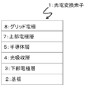
- FIG. 1 is a schematic diagram of a photoelectric conversion element according to a first embodiment. It is a cross-sectional schematic diagram of the manufacturing process of the photoelectric conversion element which concerns on 1st Embodiment. It is a cross-sectional schematic diagram of the manufacturing process of the photoelectric conversion element which concerns on 1st Embodiment. It is a cross-sectional schematic diagram of the manufacturing process of the photoelectric conversion element which concerns on 1st Embodiment. It is a cross-sectional schematic diagram of the manufacturing process of the photoelectric conversion element which concerns on 1st Embodiment.
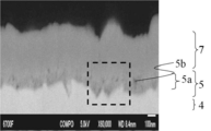
- FIG. 9 is an enlarged photograph substitution diagram within a dotted line in FIG. 8.
- It is a schematic diagram of the photoelectric conversion element which concerns on 2nd Embodiment.
- It is a cross-sectional schematic diagram of the manufacturing process of the photoelectric conversion element which concerns on 2nd Embodiment.
- It is a cross-sectional schematic diagram of the manufacturing process of the photoelectric conversion element which concerns on 2nd Embodiment.
- It is a cross-sectional schematic diagram of the manufacturing process of the photoelectric conversion element which concerns on 2nd Embodiment.
- It is a cross-sectional schematic diagram of the manufacturing process of the photoelectric conversion element which concerns on 2nd Embodiment.
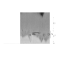
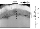
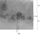
- FIG. 18 is an enlarged photograph substitute diagram within a dotted line in FIG. 17.
- the photoelectric conversion element 1 mainly includes a lower electrode layer 3, a light absorption layer 4, a semiconductor layer 5, an upper electrode layer 7, and a grid electrode 8 on a substrate 2.
- the material used for the substrate 2 examples include glass, ceramics, resin, and metal.
- a blue plate glass silica glass having a thickness of about 1 to 3 mm is used as the substrate 2.
- the lower electrode layer 3 is a conductor made of a metal such as Mo, Al, Ti, Ta or Au, or a laminated structure of these metals provided on one main surface of the substrate 2.
- the lower electrode layer 2 is formed to a thickness of about 0.2 to 1 ⁇ m using a known thin film forming method such as sputtering or vapor deposition.
- the light absorption layer 4 is a semiconductor layer having a p-type conductivity type and provided on the lower electrode layer 3 and containing, for example, a chalcopyrite-based (hereinafter also referred to as CIS-based) I-III-VI group compound. It is preferable.
- the light absorption layer 4 has a thickness of about 1 to 3 ⁇ m.
- the group I-III-VI compound is a group IB element, a group III-B element, and a group VI-B element (in other words, also referred to as a group 11, element, or group 16 element).
- Cu (In, Ga) Se 2 hereinafter also referred to as CIGS) and the like are exemplified, but the present invention is not limited thereto.
- Such a light absorbing layer 4 can be formed by a so-called vacuum process such as a sputtering method or a vapor deposition method, and a solution containing the constituent elements of the light absorbing layer 4 is applied on the lower electrode layer 3, and then It can also be formed by a so-called coating method or printing method in which drying and heat treatment are performed.
- the semiconductor layer 5 is a semiconductor layer provided on the light absorption layer 4 and having an n-type conductivity type different from the conductivity type of the light absorption layer 4.
- the semiconductor layer 5 is composed of a semiconductor layer having a compound semiconductor containing at least one of the II-B group element and the III-B group element provided on the light absorption layer 4, the semiconductor layer 5 is heterojunction with the light absorption layer 4. It is provided in the mode to do.
- the photoelectric conversion element 1 since photoelectric conversion occurs in the light absorption layer 4 and the semiconductor layer 5 constituting the heterojunction, the light absorption layer 4 and the semiconductor layer 5 are photoelectric conversion layers.
- the semiconductor layer 5 is preferably formed by a CBD method (chemical bath film formation method), for example, with a composition of In 2 S 3 system, ZnS system, CdS system, etc., and with a thickness of 1 to 30 nm. If possible, it may be formed by other means such as a thin film method or a plating method.
- CBD method chemical bath film formation method
- the upper electrode layer 7 is a transparent conductive film having an n-type conductivity provided on the semiconductor layer 5.
- the upper electrode layer 7 is provided as an electrode for extracting charges generated in the photoelectric conversion layer.
- the upper electrode layer 7 is made of a material having a resistivity lower than that of the semiconductor layer 5, such as indium oxide (ITO) containing tin, and the upper electrode layer 7 is formed by sputtering or vapor deposition. Formed by.
- ITO indium oxide
- the semiconductor layer 5 and the upper electrode layer 7 are preferably made of a material having light transmittance with respect to the wavelength region of the light absorbed by the light absorption layer 4, and the semiconductor layer 5 and the upper electrode layer 7. Are preferably substantially the same in absolute refractive index. Thereby, the fall of the light absorption efficiency to the light absorption layer 4 is suppressed.
- the grid electrode 8 including the current collector 8 a made of a metal such as Ag and the connecting portion 8 b takes out the electric charge generated in the photoelectric conversion element 1 from the upper electrode layer 7 and collects the current.
- the upper electrode layer 7 can be thinned.
- the grid electrode 8 preferably has a width of 50 to 400 ⁇ m in consideration of both conductivity and light transmittance to the light absorption layer 4.
- the semiconductor layer 5 will be described in detail.
- the semiconductor layer 5 has a porous layer region having a large number of pores on the upper electrode layer 7 side.
- the light absorption layer 4, the semiconductor layer 5 provided on the light absorption layer 4, and the upper electrode layer 7 provided on the semiconductor layer 5 are provided.
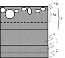
- the semiconductor layer 5 has a porous layer region 5a having a large number of holes 5b on the upper electrode layer 7 side.
- the upper electrode layer 7 is formed by the sputtering method, pinning (striking) of the sputtered particles can be trapped and prevented by the holes 5b, and damage to the light absorption layer 4 can be reduced.
- the porous layer region 5a is a layer region in which a large number of holes 5b surrounded by the semiconductor layer 5 exist, that is, a large number of closed holes 5b are distributed on the upper electrode layer 7 side. It is preferable that pinned sputtered particles are easily captured.
- the pores 5b in the porous layer region 5a are, for example, portions that appear black in the TEM analysis photographs of FIGS.
- the semiconductor layer 5 contains sulfur element and oxygen element, and S / (S + O) absorbs light when the atomic% of the sulfur element contained in the semiconductor layer 5 is S and the atomic% of the oxygen element is O. It is preferable that the layer 4 side is larger.
- S / (S + O) is preferably 0.6 to 0.79.
- Each atomic% can be measured at each part of the semiconductor layer 5 by TEM EDS analysis, and it is preferable that this range be satisfied in the vicinity of the interface of the semiconductor layer 5 with the light absorption layer 4. .
- oxygen can be reduced and sulfur can be increased in the vicinity of the pn junction, so that the pn junction can be kept good.
- the light absorption layer includes a group IB element, a group III-B element, and a group VI-B element
- the semiconductor layer includes a group III-B element and a group VI-B element
- the porosity in the porous layer region 5a is preferably 10 to 80% in terms of area ratio.
- the sputtering particles are pinned (injected) by the holes 5b.
- damage to the light absorption layer 4 can be reduced.
- the porosity is obtained by binarizing the pore 5b in the porous region 5a and the portion without the pore 5b using an image processing analyzer, and measuring and calculating the respective areas. Can be sought.
- the photoelectric conversion efficiency can be increased.
- the lower electrode layer 13, the light absorption layer 14 including a compound semiconductor capable of photoelectric conversion provided on the lower electrode layer 13, and the light absorption layer 14 are provided.
- the first semiconductor layer 15 includes a first porous layer region 15a having a large number of pores 15b on the second semiconductor layer 16 side.
- the first semiconductor layer 51 has a first porous layer region 15a having a large number of holes 15b on the second semiconductor layer 16 side.
- the first porous layer region 15a is a layer region in which a large number of holes 15b surrounded by the first semiconductor layer 15 are present, that is, a large number of closed holes 5b are present on the second semiconductor layer 16 side. It is preferable that the pinned sputtered particles are easily captured.
- the first semiconductor layer 15 contains a sulfur element and an oxygen element
- S / is the atomic% of the sulfur element contained in the first semiconductor layer 15
- O is the atomic% of the oxygen element. It is preferable that (S + O) is configured to be larger toward the light absorption layer side.
- S / (S + O) is preferably 0.5 to 0.69.
- oxygen can be reduced and sulfur can be increased in the vicinity of the pn junction, so that the pn junction can be kept good.
- the light absorption layer 14 includes a group IB element, a group III-B element, and a group VI-B element
- the first semiconductor layer 15 includes a group III-B element and a group VI-B element
- the second semiconductor layer 16 may include a II-B group element and a VI-B group element.
- the first semiconductor layer 15 includes In 2 S 3 and the second semiconductor layer 16 includes ZnO.
- the porosity in the porous region 15a is preferably 10 to 80% in terms of area ratio.
- the porosity is obtained by binarizing the pore 15b in the porous region 15a and the portion without the pore 15b using an image processing analyzer, and measuring and calculating the respective areas. Can be sought.
- the second semiconductor layer 16 is formed by a sputtering method, pinning of the sputtered particles can be trapped and prevented by the holes 15b, and damage to the light absorption layer 14 can be further reduced.
- the thickness of the porous layer region 15a is 5 to 70 nm.
- a large number of electrons existing in the upper electrode layer 17 and the second semiconductor layer 16 are kept away from the holes of the p-type layer existing in the vicinity of the pn junction between the light absorption layer 14 and the first semiconductor layer 15 by the holes 15b. Can be easily done.
- the second semiconductor layer 16 is formed by the sputtering method, pinning (implantation) of the sputtered particles can be captured by the holes 15b, and damage to the light absorption layer 14 can be appropriately reduced.
- the present embodiment provides a photoelectric conversion device using a photoelectric conversion element.
- the photoelectric conversion device 10 includes a main surface on the side where the upper electrode layers 7 and 17 and the grid electrode 8 (8a is a current collecting portion and 8b is a connecting portion) are provided.
- the photoelectric conversion elements 1 and 11 are connected in series or in parallel to form a photoelectric conversion device 10.
- photoelectric conversion device 10 of the present invention is not limited to the above-described embodiment.
- a lower electrode layer 3 made of Mo is formed by sputtering on substantially the entire surface of the cleaned substrate 2, and light absorption made of an I-III-VI group compound semiconductor is formed on the lower electrode layer 3.
- the layer 4 (for example, CIGS including Cu, In, Ga, and Se) is formed using a coating method.
- a solution for forming the light absorption layer 4 is prepared by directly dissolving a group IB metal and a group III-B metal in a solvent containing a chalcogen element-containing compound and a basic organic solvent.
- the total concentration of the group B metal and the group III-B metal is 10% by mass or more.
- Various methods such as spin coater, screen printing, dipping, spraying, and die coater can be applied to the solution.
- the chalcogen element-containing organic compound is an organic compound containing a chalcogen element.
- chalcogen element S, Se, and Te among VI-B group elements are mentioned.
- the chalcogen element-containing organic compound include thiol, sulfide, selenol, tellurol and the like.
- To directly dissolve a metal in a mixed solvent means to dissolve a single metal or alloy ingot directly into the mixed solvent and dissolve it. Drying is desirably performed in a reducing atmosphere.
- the drying temperature is, for example, 50 to 300 ° C.
- the heat treatment is desirably performed in a reducing atmosphere such as a hydrogen atmosphere or a nitrogen atmosphere in order to prevent oxidation.
- the heat treatment temperature is 400 to 600 ° C., for example.
- the semiconductor layer 5 is formed by a CBD method (chemical bath film formation method) (see FIG. 4).
- the manufacturing method of the present embodiment includes a first step of forming a light absorption layer containing a group IB element, a group III-B element and a group VI-B element on the lower electrode layer,
- the circulation flow rate of the film-forming solution and the flow rate of the bubbling nitrogen are controlled so that the average particle size of the aggregates in the film-forming solution is 300 nm or more.
- the film forming temperature is controlled to be less than 500 nm, the film forming temperature of the film forming solution is in the range of 65 ° C. or higher and lower than 70 ° C., pH 2.4 or higher and lower than pH 2.6.
- the needle-like crystals are grown individually after the epitaxial growth, and the growth is performed.
- acicular crystals are grown and fused in the in-plane direction to grow a porous layer region 5a having a large number of holes 5b on the upper electrode layer 7 side (see FIG. 5).
- ph can be controlled by adding at least one of hydrochloric acid, acetic acid and nitric acid, or aqueous ammonia.
- the average particle size can be controlled by dividing the film-forming solution by centrifugal separation.
- ITO iridium oxide
- tin or the like is formed as the upper electrode layer 7 by a sputtering method or a vapor deposition method (see FIGS. 7, 8, and 9).
- the first semiconductor layer 15 is formed by a CBD method (chemical bath film formation method).
- the second semiconductor layer 16 is formed by a sputtering method in a later process, The thickness is preferably such that the absorption layer 14 can be protected from damage (see FIG. 12).
- the manufacturing method of the present embodiment includes a first step of forming a light absorption layer 14 containing a group IB element, a group III-B element, and a group VI-B element on the lower electrode layer 13, and a light
- a first semiconductor layer 15 containing a group III-B element and a group VI-B element is formed on the absorption layer 14 by the CBD method, and the atomic% C In and sulfur atoms of the film-forming solution in the CBD method
- It is preferable to have a second step of controlling so that% C S becomes C In : C S 1: 1 to 9 (preferably 2).
- the circulation flow rate of the film forming solution and the flow rate of the bubbling nitrogen are controlled, and the average particle size of the aggregates in the film forming solution is determined.
- the film-forming temperature of the film-forming solution is controlled to be in the range of from 65 to 70 ° C. and from pH 2.4 to less than 2.6.
- the needle-like crystals are grown individually after the epitaxial growth, and the growth is performed.
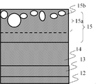
- acicular crystals are grown in the in-plane direction and fused to grow a first porous layer region 15a having a large number of holes 5b on the upper electrode layer 17 side (see FIG. 13).
- ph can be controlled by adding at least one of hydrochloric acid, acetic acid and nitric acid, or aqueous ammonia.
- the average particle size is achieved, and the particle size distribution can be managed by sizing the membrane solution by centrifugal separation.
- the sputtered particles pinned in the first porous layer region 15a can be captured (see FIGS. 14 and 15).
- ITO indium oxide containing ITO
- the upper electrode layer 17 is formed by a sputtering method or a vapor deposition method (see FIGS. 16, 17, and 18).
- Example 1 Photoelectric Conversion Element of First Embodiment (Sample Preparation)
- Example 1 relates to the case where the semiconductor layer has a single layer structure.
- a lower electrode layer 3 made of Mo is formed on substantially the entire surface of the cleaned glass substrate 2 by a sputtering method, and a light absorption layer 4 (CIGS containing Cu, In, Ga and Se) is applied on the lower electrode layer 3 Formed using.
- CIGS containing Cu, In, Ga and Se
- the concentration of the solution for forming the light absorption layer 4 was 10% by mass, applied with a spin coater, the drying temperature was 50 ° C. for 1 hour, and the heat treatment was performed in a nitrogen atmosphere at 400 ° C. for 1 hour.
- the semiconductor layer 5 was formed by the CBD method (chemical bath film formation method), and the upper electrode layer 7 was formed by the sputtering method in a later step.
- the circulation flow rate of the film-forming solution and the flow rate of the bubbling nitrogen are controlled so that the average particle size of the aggregates in the film-forming solution is 300 nm, and the film-forming solution is formed.
- the membrane temperature was controlled to 65 ° C. and pH 2.4.
- the needle-like crystals are grown during the growth process while growing the needle-like crystals individually after the epitaxial growth.
- the semiconductor layer 5 as a whole was grown to a thickness of 100 nm by growing in the in-plane direction and fusing. And the porous layer area
- ITO indium oxide
- the results are shown in Table 1 below.
- the porosity of the porous layer region 5a was controlled by the deposition rate of the porous layer region 5a, and the thickness of the porous layer region 5a was controlled by the deposition time of the porous layer region 5a.
- the semiconductor layer 5 is broken due to damage caused by pinning (striking) of the sputtered particles, and a defect is generated at the pn junction interface with the light absorption layer 4. Therefore, the photoelectric conversion efficiency was low.
- Samples 2 to 6, particularly Samples 3 to 5, showed good photoelectric conversion efficiency.
- Samples 7 to 11, particularly Samples 8 to 10 showed good photoelectric conversion efficiency, and showed a preferable range when the thickness of the porous layer region 5a was 5 to 70 nm.
- Example 2 Photoelectric Conversion Element of Second Embodiment (Sample Preparation)
- Example 2 relates to a case where the semiconductor layer has a two-layer structure.
- the process is the same as in Example 1 until the light absorption layer 14 is formed.
- the circulation flow rate of the film formation solution and the flow rate of the bubbling nitrogen are controlled so that the average particle size of the aggregates in the film formation solution is 300 nm.
- the film formation temperature of the solution was controlled to 65 ° C. and pH 2.4.
- the needle-like crystals are grown during the growth process while growing the needle-like crystals individually after the epitaxial growth.
- the porous layer region 15a having a large number of pores 15b on the second semiconductor layer 16 side is grown in the in-plane direction and fused, and the semiconductor layer 5 as a whole has a thickness of 100 nm.
- i-ZnO high resistance zinc oxide
- ITO indium oxide
- the circulation flow rate of the film formation solution and the flow rate of the bubbling nitrogen are controlled, and the average particle size of the aggregates in the film formation solution is 300 nm.
- the film-forming temperature of the film-forming solution is controlled to be 65 ° C. and pH 2.4
- the film formation is stopped before the acicular crystals are generated, and high resistance zinc oxide (i -ZnO) was prepared by forming indium oxide (ITO) as the upper electrode layer 7 by the sputtering method, so that the sample 12 having no porous layer region 15a was obtained.
- the results are shown in Table 2 below.
- the porosity of the first porous layer region 15a is the film formation speed of the first porous layer region 15a
- the thickness of the first porous layer region 15a is the film formation time of the first porous layer region 15a. Respectively.
- the first semiconductor layer 15 is broken due to damage due to pinning (implantation) of the sputtered particles, and the pn junction interface with the light absorption layer 14 is formed. Since a defect occurred, the photoelectric conversion efficiency was low.
- Samples 13 to 17, particularly Samples 14 to 16, showed good photoelectric conversion efficiency.
- Samples 18-22 showed good photoelectric conversion efficiency, and the thickness of the porous layer region 5a was found to be in a suitable range when it was 5-70 nm.
Landscapes
- Photovoltaic Devices (AREA)
- Recrystallisation Techniques (AREA)
Abstract
【課題】透明電極に存在する多数の電子が、光吸収層のホールに近いと、経年変化でpn接合界面での欠陥が増加する場合があった。 【解決手段】下部電極層と、この下部電極層上に設けられた、光電変換可能な化合物半導体を含む光吸収層と、この光吸収層上に設けられた半導体層と、この半導体層上に設けられた、この半導体層よりも抵抗率が低い上部電極層とを有する光電変換素子であって、前記半導体層は、前記上部電極層側に、多数の空孔を有する多孔質層領域を有する。
Description
本発明は光電変換素子および光電変換装置に関する。
太陽光発電などに使用される光電変換装置としては、光吸収係数が高いCIGSなどのカルコパイライト系のI-III-VI族化合物半導体によって光吸収層が形成されたものがある。CIGSは光吸収係数が高く、光電変換装置の薄膜化や大面積化や低コスト化に適しており、これを用いた次世代太陽電池の研究開発が進められている。
その光電変換素子は、ガラスなどの基板上に、金属電極などの下部電極と、光吸収層やバッファ層などを含む半導体層である光電変換層と、透明電極や金属電極などの上部電極とが、この順に積層されて構成される。そして、複数の光電変換素子は、隣り合う一方の光電変換素子の上部電極と他方の光電変換素子の下部電極とが、接続導体によって電気的に接続されることで、電気的に直列に接続されている。
このような光電変換素子は、例えば、光吸収層上に化学析出法によりCdSを厚さ10nmに析出させて、バッファ層を形成し、このバッファ層上にZnOターゲットとMgOターゲットの二元ターゲットを用いたスパッタリング法により、Zn0.85Mg0.15Oから成る1.2μmの膜厚の上部電極層を形成することによって作製されることが知られている(例えば特許文献1参照)。
しかしながら、特許文献1に開示された光電変換素子では、光吸収層等へスパッタリング粒子が打ち込まれることによってダメージを受け、光電変換効率を十分に高めることが困難であった。
また、透明電極に存在する多数の電子が、光吸収層のホールに近いと、電子とホールが再結合し易くなる傾向があり、光電変換効率を十分に高めることが困難であった。
よって本発明は、光電変換素子および光電変換装置の光電変換効率を高めることを目的とする。
上記に鑑みて本発明の一実施形態に係る光電変換素子は、下部電極層と、該下部電極層上に設けられた、光電変換可能な化合物半導体を含む光吸収層と、該光吸収層上に設けられた半導体層と、該半導体層上に設けられた、該半導体層よりも抵抗率が低い上部電極層とを有する光電変換素子であって、前記半導体層は、前記上部電極層側に、多数の空孔を有する多孔質層領域を有する。
また、本発明の他の一実施形態に係る光電変換素子は、下部電極層と、該下部電極層上に設けられた、光電変換可能な化合物半導体を含む光吸収層と、該光吸収層上に設けられた第1半導体層と、該第1半導体層上に設けられた第2半導体層と、該第2半導体層上に設けられた、該第2半導体層よりも抵抗率が低い上部電極層とを有する光電変換素子であって、前記第1半導体層は、前記第2半導体層側に、多数の空孔を有する第1多孔質層領域を有する。
また、本発明の他の一実施形態に係る光電変換装置は、前記光電変換素子を用いたものである。
本発明の光電変換素子および光電変換装置によれば、光吸収層等へスパッタリング粒子が打ち込まれることによるダメージを低減し、光電変換効率を高めることができる。
また、上部電極に存在する多数の電子を、半導体層に空孔を有する分だけ、光吸収層のホールから遠ざけることができるので、電子とホールとの再結合を低減して光電変換効率を高めることができる。
以下、本発明の一実施形態を図面に基づいて説明する。
<第1実施形態に係る光電変換素子>
図2において光電変換素子1は、基板2上に下部電極層3と、光吸収層4と、半導体層5と、上部電極層7と、グリッド電極8とを主として備えている。
図2において光電変換素子1は、基板2上に下部電極層3と、光吸収層4と、半導体層5と、上部電極層7と、グリッド電極8とを主として備えている。
基板2に用いられる材料としては、ガラス、セラミックス、樹脂および金属などが挙げられる。ここでは、基板2として、厚さ1~3mm程度の青板ガラス(ソーダライムガラス)が用いられている。
下部電極層3は、基板2の一主面上に設けられた、Mo、Al、Ti、TaまたはAuなどの金属、あるいはこれらの金属の積層構造体からなる導体である。下部電極層2は、スパッタリング法または蒸着法などの公知の薄膜形成方法を用いて、0.2~1μm程度の厚みに形成される。
光吸収層4は、下部電極層3の上に設けられた、例えばカルコパイライト系(以下CIS系とも言う)のI-III-VI族化合物を含む、p型の導電型を有する半導体層であることが好ましい。この光吸収層4は、1~3μm程度の厚みを有している。ここで、I-III-VI族化合物とは、I-B族元素と、III-B族元素とVI-B族元素(換言すれば、11族元素、13族元素、16族元素ともいう)との化合物であり、本実施形態としては、Cu(In、Ga)Se2(以下、CIGSとも言う)などが挙げられるが、これらに限定されるものではない。このような光吸収層4については、スパッタリング法、蒸着法などのいわゆる真空プロセスによって形成可能であるほか、光吸収層4の構成元素を含む溶液を下部電極層3の上に塗布し、その後、乾燥・熱処理を行う、いわゆる塗布法あるいは印刷法と称されるプロセスによって形成することもできる。
半導体層5は、光吸収層4の上に設けられた、該光吸収層4の導電型とは異なるn型の導電型を有する半導体層である。半導体層5は光吸収層4上に設けられたII-B族元素、III-B族元素の少なくとも1つを含む化合物半導体を有する半導体層によって構成される場合に、光吸収層4とヘテロ接合する態様で設けられる。光電変換素子1では、このヘテロ接合を構成する光吸収層4と半導体層5とにおいて光電変換が生じることから、光吸収層4と半導体層5とが光電変換層となっている。また、半導体層5はCBD法(ケミカルバス成膜法)によって、例えば、In2S3系、ZnS系、CdS系等の組成で構成され、1~30nmの厚みに形成されることが好ましいが、可能であれば薄膜法、メッキ法などの他の手段によって形成されても構わない。
上部電極層7は、半導体層5の上に設けられた、n型の導電型を有する透明導電膜である。上部電極層7は、光電変換層において生じた電荷を取り出す電極として設けられている。また、上部電極層7は、半導体層5よりも低い抵抗率を有する物質、例えば錫を含んだ酸化インジウム(ITO)などによって構成されるものであり、上部電極層7は、スパッタリング法、蒸着法などによって形成される。
なお、半導体層5、上部電極層7は、光吸収層4が吸収する光の波長領域に対して光透過性を有する物質によって構成されることが好ましく、また、半導体層5、上部電極層7は、絶対屈折率が略同一であることが好ましい。これにより、光吸収層4までの光の吸収効率の低下が抑制される。
そして、図1に示されるような、Agなどの金属からなる集電部8aと連結部8bとからなるグリッド電極8は、光電変換素子1において発生した電荷を上部電極層7から取り出して集電する役割を担うものであり、これにより上部電極層7の薄層化が可能となる。グリッド電極8は、導電性と、光吸収層4への光透過性との両立を考慮すると、50~400μmの幅を有することが好ましい。
上記半導体層5について詳細に説明する。
第1実施形態において、半導体層5は、上部電極層7側に、多数の空孔を有する多孔質層領域を有する。
例えば、図6および図7に示されるように、光吸収層4と、光吸収層4上に設けられた半導体層5と、半導体層5上に設けられた上部電極層7とを有しており、半導体層5は、上部電極層7側に、多数の空孔5bを有する多孔質層領域5aを有する。
これによって、上部電極7に存在する多数の電子を、半導体層5に空孔5bを有する分だけ、光吸収層4のホールから遠ざけることができるので、電子とホールとの再結合を低減して光電変換効率を高めることができる。
さらに、上部電極層7をスパッタリング法で形成する際に、スパッタリング粒子のピンニング(打ち込み)を空孔5bでトラップして防いで、光吸収層4へのダメージを低減することができる。
ここで多孔質層領域5aとは、半導体層5で囲まれた空孔5bが多数存在する層領域であること、すなわち閉気孔である空孔5bが多数、上部電極層7側に分布していることが、ピンニングされたスパッタリング粒子を捕捉し易い点で好ましい。
またここで、多孔質層領域5aの空孔5bとは、例えば、図8および図9のTEM分析写真において、黒く見える部分である。
本実施形態では、半導体層5は硫黄元素および酸素元素を含み、半導体層5に含まれる硫黄元素の原子%をS、酸素元素の原子%をOとしたとき、S/(S+O)が光吸収層4側ほど大きいことが好ましい。
さらに、多孔質層領域5aにおいて、S/(S+O)が0.6~0.79であることが好ましい。
各原子%は半導体層5の各部位においてTEMのEDS分析で測定可能であり、半導体層5における光吸収層4との界面付近において、この範囲を満足することが好ましい。
これにより、pn接合付近では酸素を少なく、硫黄を多くできるので、pn接合を良好に保つことができる。
本実施形態は、光吸収層がI-B族元素、III-B族元素およびVI-B族元素を含み、半導体層がIII-B族元素およびVI-B族元素を含む。
これにより、上部電極層7のスパッタリング粒子が光吸収層4へダメージを与えることを低減することができる。
本実施形態では、多孔質層領域5aにおける空孔率は、面積比で10~80%であることが好ましい。
これにより、半導体層5の多孔質領域5aと上部電極層7との密着性を維持しつつ、上部電極層7をスパッタリング法で形成する際に、スパッタリング粒子のピンニング(打ち込み)を空孔5bでトラップして防いで、光吸収層4へのダメージを低減することができる。
ここで空孔率は、多孔質領域5aにおける空孔5bと、空孔5bが無い部分とに、画像処理解析装置を使用して2値化処理し、それぞれの面積を測定、演算することによって求めることができる。
また、上部電極層7に存在する多数の電子を、半導体層5に空孔5bを有する分だけ、光吸収層4のホールから遠ざけることができるので、光電変換効率を高めることができる。
<第2実施形態に係る光電変換素子>
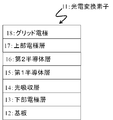
第2実施形態において、図10に示すように、下部電極層13と、下部電極層13上に設けられた、光電変換可能な化合物半導体を含む光吸収層14と、光吸収層14上に設けられた第1半導体層15と、第1半導体層15上に設けられた第2半導体層16と、第2半導体層16上に設けられた、第2半導体層16よりも抵抗率が低い上部電極層17とを有する光電変換素子11であって、第1半導体層15は、第2半導体層16側に、多数の空孔15bを有する第1多孔質層領域15aを有する。
第2実施形態において、図10に示すように、下部電極層13と、下部電極層13上に設けられた、光電変換可能な化合物半導体を含む光吸収層14と、光吸収層14上に設けられた第1半導体層15と、第1半導体層15上に設けられた第2半導体層16と、第2半導体層16上に設けられた、第2半導体層16よりも抵抗率が低い上部電極層17とを有する光電変換素子11であって、第1半導体層15は、第2半導体層16側に、多数の空孔15bを有する第1多孔質層領域15aを有する。
すなわち、図17、図18に示されるように、光吸収層14と、光吸収層14上に設けられた第1半導体層15と、第1半導体層15上に設けられた第2半導体層16とを有しており、第1半導体層51は、第2半導体層16側に、多数の空孔15bを有する第1多孔質層領域15aを有する。
これによって、上部電極層17に存在する多数の電子を、第1半導体層15に空孔15bを有する分だけ、光吸収層14のホールから遠ざけることができるので、電子とホールとの再結合を低減して光電変換効率を高めることができる。
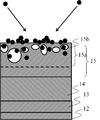
さらに、第2半導体層16をスパッタリング法で形成する際に、スパッタリング粒子のピンニング(打ち込み)を空孔15bでトラップして防いで、光吸収層14へのダメージを低減することができる。ここで第1多孔質層領域15aは、第1半導体層15で囲まれた空孔15bが多数存在する層領域であること、すなわち閉気孔である空孔5bが多数、第2半導体層16側に分布していることが、ピンニングされたスパッタリング粒子を捕捉し易い点で好ましい。
さらに、本実施形態は、第1半導体層15は硫黄元素および酸素元素を含み、第1半導体層15に含まれる硫黄元素の原子%をS、酸素元素の原子%をOとしたとき、S/(S+O)が光吸収層側ほど大きい構成であることが好ましい。
さらに、多孔質層領域15aにおいて、S/(S+O)が0.5~0.69であることが好ましい。
これにより、pn接合付近では酸素を少なく、硫黄を多くできるので、pn接合を良好に保つことができる。
さらに、本実施形態は、光吸収層14がI-B族元素、III-B族元素およびVI-B族元素を含み、第1半導体層15がIII-B族元素およびVI-B族元素を含み、第2半導体層16がII-B族元素およびVI-B族元素を含んでもよい。
より好ましくは、第1半導体層15はIn2S3を含み、第2半導体層16はZnOを含む。
これにより、第2半導体層16の例えばZnOのスパッタリング粒子が光吸収層14へダメージを与えることを低減することができ、さらに、ZnOのZnが第1半導体層15を介して光吸収層14に経年変化によって拡散していき、pn接合を良好に行うことができる。
さらに、本実施形態は、多孔質領域15aにおける空孔率は、面積比で10~80%であることが好ましい。
これによって、上部電極層17に存在する多数の電子を、半導体層15に空孔15bを有する分だけ、光吸収層14のホールから遠ざけることができるので、電子とホールとの再結合をより低減して、光電変換効率を高めることができる。
ここで空孔率は、多孔質領域15aにおける空孔15bと、空孔15bが無い部分とに、画像処理解析装置を使用して2値化処理し、それぞれの面積を測定、演算することによって求めることができる。
さらに、第2半導体層16をスパッタリング法で形成する際に、スパッタリング粒子のピンニング(打ち込み)を空孔15bでトラップして防いで、光吸収層14へのダメージをより低減することができる。
さらに、本実施形態は、多孔質層領域15aの厚さが5~70nmである。
空孔15bにより、上部電極層17および第2半導体層16に存在する多数の電子を、光吸収層14と第1半導体層15とのpn接合付近に存在するp型層のホールから遠ざけておくことが容易にできる。
また、第2半導体層16をスパッタリング法で形成する際に、スパッタリング粒子のピンニング(打ち込み)を空孔15bで捕捉して、光吸収層14へのダメージを適切に低減することができる。
<光電変換装置>
本実施形態は、光電変換素子を用いた光電変換装置を提供するものである。
本実施形態は、光電変換素子を用いた光電変換装置を提供するものである。
図1に示す例のように、光電変換装置10は、上部電極層7、17およびグリッド電極8(8aは集電部、8bは接続部)が設けられた側の主面が受光面側となっており、それぞれの光電変換素子1、11が直列あるいは並列接続されて光電変換装置10となっている。
上記した光電変換素子1、11を光電変換装置10に用いて、さらに高い光電変換効率を提供することが容易になる。
なお、本発明の光電変換装置10は上記のような一実施形態に限られたものではない。
<光電変換素子の製造方法>
以下において、光電変換素子の第1実施形態の製造方法、および第2実施形態の製造方法の説明をそれぞれ説明する。
以下において、光電変換素子の第1実施形態の製造方法、および第2実施形態の製造方法の説明をそれぞれ説明する。
(第1実施形態の光電変換素子の製造方法)
I-III-VI族化合物半導体からなる光吸収層4(例えば、Cu、In、GaおよびSeを含むCIGS等)が塗布法を用いて形成され、さらに、半導体層5以降が形成される場合を例として説明する。
I-III-VI族化合物半導体からなる光吸収層4(例えば、Cu、In、GaおよびSeを含むCIGS等)が塗布法を用いて形成され、さらに、半導体層5以降が形成される場合を例として説明する。
まず、図3のように、洗浄された基板2の略全面に、Moからなる下部電極層3がスパッタリング法で形成され、下部電極層3上にI-III-VI族化合物半導体からなる光吸収層4(例えば、Cu、In、GaおよびSeを含むCIGS等)が塗布法を用いて形成される。
ここで、光吸収層4を形成するための溶液が下部電極層3の表面に塗布され、乾燥によって被膜が形成された後、この被膜が熱処理されることで、光吸収層4が形成される。光吸収層4を形成するための溶液は、カルコゲン元素含有機化合物と塩基性有機溶剤とを含む溶媒に、I-B族金属およびIII-B族金属を直接溶解することで作製され、I-B族金属およびIII-B族金属の合計濃度が10質量%以上の溶液とされる。なお、溶液の塗布にはスピンコーター、スクリーン印刷、ディッピング、スプレー、ダイコーターなど様々な方法の適用が可能である。カルコゲン元素含有有機化合物とは、カルコゲン元素を含む有機化合物である。カルコゲン元素としては、VI-B族元素のうちのS、Se、Teをいう。カルコゲン元素含有有機化合物としては、例えば、チオール、スルフィド、セレノール、テルロール等が挙げられる。金属を混合溶媒に直接溶解させるというのは、単体金属または合金の地金を、直接、混合溶媒に混入し、溶解させることをいう。乾燥は、還元雰囲気下で行われることが望ましい。乾燥温度は、例えば50~300℃である。熱処理は、酸化防止のために水素雰囲気や窒素雰囲気などの還元雰囲気下で行われることが望ましい。熱処理温度は、例えば400~600℃である。
光吸収層4が形成された後、半導体層5はCBD法(ケミカルバス成膜法)によって形成される(図4を参照)。
ここで本実施形態の製造方法は、下部電極層上に、I-B族元素、III-B族元素およびVI-B族元素を含む光吸収層を形成する第1工程と、光吸収層上に、III-B族元素およびVI-B族元素を含む第1半導体層をCBD法で形成するとともに、CBD法における成膜用溶液のInの原子%CInと硫黄の原子%CSとが、CIn:CS=1:1~9(好ましくは2)となるように制御する第2工程とを有することが好ましい。
そしてこの第2工程では、半導体層5のエピタキシャル成長中に、成膜用溶液の循環流量と、そのバブリング用窒素の流量とを制御し、成膜用溶液中の凝集物の平均粒径を300nm以上500nm未満、成膜用溶液の成膜温度を65℃以上70℃未満、pH2.4以上pH2.6未満の範囲となるように管理する。
そして、成膜用溶液中の凝集物の平均粒径を3μm以上、成膜用溶液をpH2.6以上2.8未満に切り替えることによって、エピタキシャル成長後に針状結晶を個別に成長させつつ、その成長過程で針状結晶を面内方向に成長させて融合させ、上部電極層7側に多数の空孔5bを有する多孔質層領域5aを成長させる(図5を参照)。
これにより、周囲が第1半導体層5のみで囲まれた空孔5bを得ることができる。
ここで、phは塩酸、酢酸、硝酸の少なくともいずれかの酸もしくはアンモニア水を添加することによって制御することができる。
また、平均粒度は、成膜用溶液を遠心分離法で分粒することによって、粒度分布を管理することができる。
そして、上部電極層7をスパッタリング法で形成する際に、多孔質層領域5aによってスパッタリング粒子のピンニングを捕捉することができる(図6を参照)。
そして、上部電極層7として錫を含んだ酸化イジウム(ITO)などが、スパッタリング法、蒸着法で形成される(図7、図8および図9を参照)。
(第2実施形態の光電変換素子の製造方法)
ここでは光吸収層14までの形成は、上記第1実施形態と同様である。
ここでは光吸収層14までの形成は、上記第1実施形態と同様である。
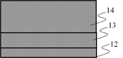
光吸収層14が形成された後、第1半導体層15はCBD法(ケミカルバス成膜法)によって形成されるが、後工程で第2半導体層16をスパッタリング法で形成する場合には、光吸収層14をダメージから保護できる厚みであることが好ましい(図12を参照)。
ここで、本実施形態の製造方法は、下部電極層13上に、I-B族元素、III-B族元素およびVI-B族元素を含む光吸収層14を形成する第1工程と、光吸収層14上に、III-B族元素およびVI-B族元素を含む第1半導体層15をCBD法で形成するとともに、CBD法における成膜用溶液のInの原子%CInと硫黄の原子%CSとが、CIn:CS=1:1~9(好ましくは2)となるように制御する第2工程とを有することが好ましい。
そしてこの第2工程では、第1半導体層15のエピタキシャル成長中に、成膜用溶液の循環流量と、そのバブリング用窒素の流量とを制御し、成膜用溶液中の凝集物の平均粒径を300nm以上500nm未満、成膜用溶液の成膜温度を65℃以上70℃未満、pH2.4以上pH2.6未満の範囲となるように管理する。
そして、成膜用溶液中の凝集物の平均粒径を3μm以上、成膜用溶液をpH2.6以上2.8未満に切り替えることによって、エピタキシャル成長後に針状結晶を個別に成長させつつ、その成長過程で針状結晶を面内方向に成長させて融合させ、上部電極層17側に多数の空孔5bを有する第1多孔質層領域15aを成長させる(図13を参照)。
これにより、周囲が第1半導体層15のみで囲まれた空孔15bを得ることができる。
ここで、phは塩酸、酢酸、硝酸の少なくともいずれかの酸もしくはアンモニア水を添加することによって制御することができる。
また、平均粒度は成、膜用溶液を遠心分離法で分粒することによって、粒度分布を管理することができる。
そして、第2半導体層16をスパッタリング法で形成する際に、第1多孔質層領域15aにおいてピンニングされたスパッタリング粒子を捕捉することができる(図14および図15を参照)。
そして、上部電極層17として錫を含んだ酸化インジウム(ITO)などが、スパッタリング法、蒸着法で形成される(図16、図17および図18を参照)。
(実施例1)第1実施形態の光電変換素子
(試料作製)
本実施例1は、半導体層が単層構造である場合に関するものである。
(試料作製)
本実施例1は、半導体層が単層構造である場合に関するものである。
洗浄されたガラス基板2の略全面に、Moからなる下部電極層3をスパッタリング法で形成し、下部電極層3上に光吸収層4(Cu、In、GaおよびSeを含むCIGS)を塗布法を用いて形成した。
光吸収層4を形成するための溶液の濃度は10質量%とし、スピンコーターで塗布して、乾燥温度は50℃で1時間、熱処理は窒素雰囲気下で400℃で1時間とした。
光吸収層4が形成された後、半導体層5はCBD法(ケミカルバス成膜法)によって形成し、後工程で上部電極層7をスパッタリング法で形成した。
そして、半導体層5のエピタキシャル成長中に、成膜用溶液の循環流量と、そのバブリング用窒素の流量を制御し、成膜用溶液中の凝集物の平均粒径を300nm、成膜用溶液の成膜温度を65℃、pH2.4となるように管理した。そして、成膜用溶液中の凝集物の平均粒径を3μm、成膜用溶液をpH2.6に切り替えることによって、エピタキシャル成長後に針状結晶を個別に成長させつつ、その成長過程で針状結晶を面内方向に成長させて融合させ、半導体層5全体としては100nm厚とした。そして、上部電極層7側に多数の空孔5bを有する多孔質層領域5aを成長させ、上部電極層7として酸化インジウム(ITO)をスパッタリング法で形成した。
比較例1として、半導体層5のエピタキシャル成長中に、成膜用溶液の循環流量と、そのバブリング用窒素の流量とを制御し、成膜用溶液中の凝集物の平均粒径を300nm、成膜用溶液の成膜温度を65℃、pH2.4となるように管理した後に、針状結晶が発生する前に成膜を止めて、上部電極層7として酸化インジウム(ITO)をスパッタリング法で形成したことで、多孔質層領域5aを有さない試料1とした。
以下、結果を表1に示す。なお多孔質層領域5aの空孔率は、多孔質層領域5aの成膜速度で、多孔質層領域5aの厚さは、多孔質層領域5aの成膜時間でそれぞれ制御した。

比較例である試料1では、上部電極層7をスパッタリング法で形成したとき、スパッタリング粒子のピンニング(打ち込み)によるダメージによって、半導体層5が壊れて光吸収層4とのpn接合界面に欠陥が生じていたため、光電変換効率が低かった。
試料2~6において、特に試料3~5では良好な光電変換効率を示した。
また試料7~11において、特に試料8~10では良好な光電変換効率を示し、多孔質層領域5aの厚さは5~70nmである場合に、好適範囲を示すことがわかった。
なお、本実施例である試料2~11の断面をTEMで観察すれば、半導体層5の上部電極層7側に空孔5bが多く分布していた。
(実施例2)第2実施形態の光電変換素子
(試料作製)
本実施例2は、半導体層が2層構造である場合に関するものである。
(試料作製)
本実施例2は、半導体層が2層構造である場合に関するものである。
光吸収層14を形成するまでは実施例1と同様である。
そして、第1半導体層15のエピタキシャル成長中に、成膜用溶液の循環流量と、そのバブリング用窒素の流量とを制御し、成膜用溶液中の凝集物の平均粒径を300nm、成膜用溶液の成膜温度を65℃、pH2.4となるように管理した。
そして、成膜用溶液中の凝集物の平均粒径を3μm、成膜用溶液をpH2.6に切り替えることによって、エピタキシャル成長後に針状結晶を個別に成長させつつ、その成長過程で針状結晶を面内方向に成長させて融合させ、第2半導体層16側に多数の空孔15bを有する多孔質層領域15aを成長させ、半導体層5全体としては100nm厚とした。
そして、第2半導体層16として高抵抗な酸化亜鉛(i-ZnO)を、上部電極層17として酸化インジウム(ITO)をスパッタリング法で形成した。
比較例1として、第1半導体層15のエピタキシャル成長中に、成膜用溶液の循環流量と、そのバブリング用窒素の流量とを制御し、成膜用溶液中の凝集物の平均粒径を300nm、成膜用溶液の成膜温度を65℃、pH2.4となるように管理した後に、針状結晶が発生する前に成膜を止めて、第2半導体層16として高抵抗な酸化亜鉛(i-ZnO)を、上部電極層7として酸化インジウム(ITO)をスパッタリング法で形成したことで、多孔質層領域15aを有さない試料12とした。
以下、結果を表2に示す。なお第1多孔質層領域15aの空孔率は、第1多孔質層領域15aの成膜速度で、第1多孔質層領域15aの厚さは、第1多孔質層領域15aの成膜時間でそれぞれ制御した。
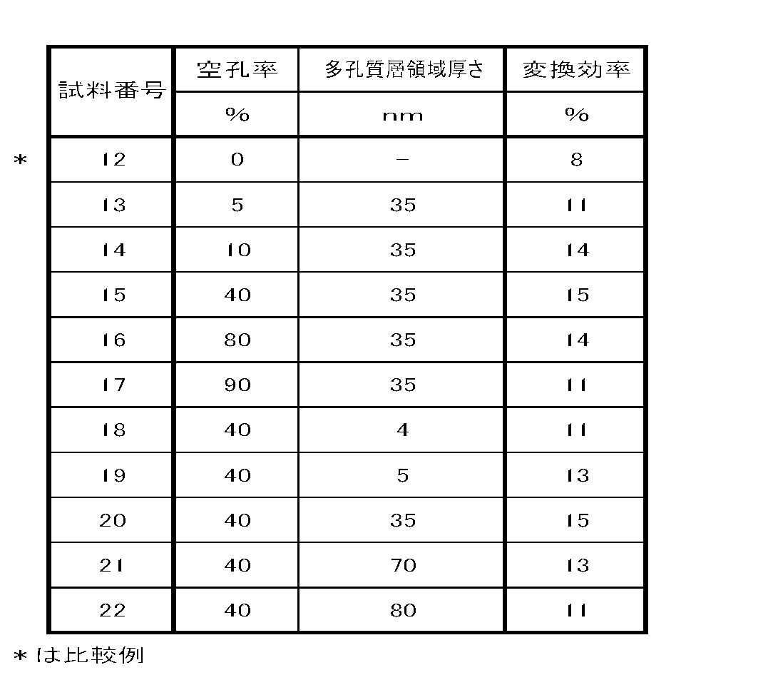
比較例である試料12では、第2半導体層16をスパッタリング法で形成したとき、スパッタリング粒子のピンニング(打ち込み)によるダメージによって、第1半導体層15が壊れて光吸収層14とのpn接合界面に欠陥が生じていたため、光電変換効率が低かった。
試料13~17において、特に試料14~16では良好な光電変換効率を示した。
また試料18~22において、特に試料19~21では良好な光電変換効率を示し、多孔質層領域5aの厚さは、5~70nmである場合に、好適範囲であることがわかった。
なお、本実施例である試料13~22の断面をTEMで観察したところ、第1半導体層5の第2半導体層6側に空孔5bが多く分布していた。
1、11:光電変換素子
2、12:基板
3、13:下部電極層
4、14:光吸収層
5:半導体層
5a:多孔質層領域
5b:空孔
15:第1半導体層
15a:第1多孔質層領域
15b:空孔
16:第2半導体層
7、17:上部電極層
8:グリッド電極
2、12:基板
3、13:下部電極層
4、14:光吸収層
5:半導体層
5a:多孔質層領域
5b:空孔
15:第1半導体層
15a:第1多孔質層領域
15b:空孔
16:第2半導体層
7、17:上部電極層
8:グリッド電極
Claims (11)
- 下部電極層と、該下部電極層上に設けられた、光電変換可能な化合物半導体を含む光吸収層と、該光吸収層上に設けられた半導体層と、該半導体層上に設けられた、該半導体層よりも電気抵抗率が低い上部電極層とを有する光電変換素子であって、
前記半導体層は、前記上部電極層側に、多数の空孔を有する多孔質層領域を有する光電変換素子。 - 前記半導体層は硫黄元素および酸素元素を含み、前記半導体層に含まれる硫黄元素の原子%をS、酸素元素の原子%をOとしたとき、S/(S+O)が前記光吸収層側ほど大きい、請求項1に記載の光電変換素子。
- 前記光吸収層がI-B族元素、III-B族元素およびVI-B族元素を含み、前記半導体層がIII-B族元素およびVI-B族元素を含む、請求項1または2に記載の光電変換素子。
- 前記多孔質層領域における空孔率は、面積比で10~80%である、請求項1~3のいずれかに記載の光電変換素子。
- 下部電極層と、該下部電極層上に設けられた、光電変換可能な化合物半導体を含む光吸収層と、該光吸収層上に設けられた第1半導体層と、該第1半導体層上に設けられた第2半導体層と、該第2半導体層上に設けられた、該第2半導体層よりも抵抗率が低い上部電極層とを有する光電変換素子であって、
前記第1半導体層は、前記第2半導体層側に、多数の空孔を有する第1多孔質層領域を有する、光電変換素子。 - 前記第1半導体層は硫黄元素および酸素元素を含み、前記第1半導体層に含まれる硫黄元素の原子%をS、酸素元素の原子%をOとしたとき、S/(S+O)が前記光吸収層側ほど大きい、請求項5に記載の光電変換素子。
- 前記光吸収層がI-B族元素、III-B族元素およびVI-B族元素を含み、前記第1半導体層がIII-B族元素およびVI-B族元素を含み、前記第2半導体層上がII-B族元素およびVI-B族元素を含む、請求項5または6に記載の光電変換素子。
- 前記第1半導体層はIn2S3を含み、前記第2半導体層はZnOを含む、請求項5~7のいずれかに記載の光電変換素子。
- 前記第1多孔質領域における空孔率は、面積比で10~80%である、請求項5~8のいずれかに記載の光電変換素子。
- 前記多孔質層領域の厚さは5~70nmである、請求項1~9のいずれかに記載の光電変換素子。
- 請求項1~10のいずれかに記載の光電変換素子を用いた光電変換装置。
Priority Applications (1)
| Application Number | Priority Date | Filing Date | Title |
|---|---|---|---|
| JP2013501161A JPWO2012115267A1 (ja) | 2011-02-25 | 2012-02-27 | 光電変換素子および光電変換装置 |
Applications Claiming Priority (4)
| Application Number | Priority Date | Filing Date | Title |
|---|---|---|---|
| JP2011040261 | 2011-02-25 | ||
| JP2011-040261 | 2011-02-25 | ||
| JP2011164178 | 2011-07-27 | ||
| JP2011-164178 | 2011-07-27 |
Publications (1)
| Publication Number | Publication Date |
|---|---|
| WO2012115267A1 true WO2012115267A1 (ja) | 2012-08-30 |
Family
ID=46721034
Family Applications (1)
| Application Number | Title | Priority Date | Filing Date |
|---|---|---|---|
| PCT/JP2012/054771 Ceased WO2012115267A1 (ja) | 2011-02-25 | 2012-02-27 | 光電変換素子および光電変換装置 |
Country Status (2)
| Country | Link |
|---|---|
| JP (1) | JPWO2012115267A1 (ja) |
| WO (1) | WO2012115267A1 (ja) |
Cited By (1)
| Publication number | Priority date | Publication date | Assignee | Title |
|---|---|---|---|---|
| JP2013012703A (ja) * | 2011-05-30 | 2013-01-17 | Kyocera Corp | 化合物半導体膜の製造方法および製造装置 |
Citations (4)
| Publication number | Priority date | Publication date | Assignee | Title |
|---|---|---|---|---|
| JPS5730379A (en) * | 1980-07-31 | 1982-02-18 | Agency Of Ind Science & Technol | Thin film solar battery |
| JPH0541531A (ja) * | 1991-05-27 | 1993-02-19 | Fuji Electric Corp Res & Dev Ltd | CuInSe2 系薄膜太陽電池およびその製造方法 |
| JP2006525671A (ja) * | 2003-05-08 | 2006-11-09 | ソリブロ エイビー | 薄膜太陽電池 |
| JP2010287607A (ja) * | 2009-06-09 | 2010-12-24 | Hitachi Ltd | タンデム型薄膜太陽電池 |
-
2012
- 2012-02-27 JP JP2013501161A patent/JPWO2012115267A1/ja active Pending
- 2012-02-27 WO PCT/JP2012/054771 patent/WO2012115267A1/ja not_active Ceased
Patent Citations (4)
| Publication number | Priority date | Publication date | Assignee | Title |
|---|---|---|---|---|
| JPS5730379A (en) * | 1980-07-31 | 1982-02-18 | Agency Of Ind Science & Technol | Thin film solar battery |
| JPH0541531A (ja) * | 1991-05-27 | 1993-02-19 | Fuji Electric Corp Res & Dev Ltd | CuInSe2 系薄膜太陽電池およびその製造方法 |
| JP2006525671A (ja) * | 2003-05-08 | 2006-11-09 | ソリブロ エイビー | 薄膜太陽電池 |
| JP2010287607A (ja) * | 2009-06-09 | 2010-12-24 | Hitachi Ltd | タンデム型薄膜太陽電池 |
Cited By (1)
| Publication number | Priority date | Publication date | Assignee | Title |
|---|---|---|---|---|
| JP2013012703A (ja) * | 2011-05-30 | 2013-01-17 | Kyocera Corp | 化合物半導体膜の製造方法および製造装置 |
Also Published As
| Publication number | Publication date |
|---|---|
| JPWO2012115267A1 (ja) | 2014-07-07 |
Similar Documents
| Publication | Publication Date | Title |
|---|---|---|
| US20110018089A1 (en) | Stack structure and integrated structure of cis based solar cell | |
| JP5928612B2 (ja) | 化合物半導体太陽電池 | |
| CN1350335A (zh) | 太阳能电池 | |
| JP2004296749A (ja) | 両面受光太陽電池 | |
| JP5178904B1 (ja) | Czts系薄膜太陽電池及びその製造方法 | |
| JP2001044464A (ja) | Ib―IIIb―VIb2族化合物半導体層の形成方法、薄膜太陽電池の製造方法 | |
| KR20080009346A (ko) | 태양전지 버퍼층의 제조방법 | |
| CN102628161A (zh) | 用于制造半导体膜和光伏装置的方法 | |
| JPWO2011136249A1 (ja) | 光電変換素子および光電変換装置ならびに光電変換素子の製造方法 | |
| US20130029450A1 (en) | Method for manufacturing solar cell | |
| KR101300791B1 (ko) | 전자빔 조사를 이용한 몰리브덴 박막의 전도도 향상 방법 | |
| JP2011119478A (ja) | 化合物半導体太陽電池 | |
| WO2012115267A1 (ja) | 光電変換素子および光電変換装置 | |
| JP5641850B2 (ja) | 光電変換素子およびその製造方法 | |
| CN102447008A (zh) | 光伏器件及其制造方法 | |
| CN102473768A (zh) | 太阳能电池及其制造方法 | |
| JP2012151432A (ja) | 光電変換素子および光電変換装置ならびに光電変換素子の製造方法 | |
| WO2012115265A1 (ja) | 光電変換素子および光電変換装置 | |
| US20180240918A1 (en) | Photovoltaic devices including a chalcogenide-containing photovoltaic light-absorber, and related methods of making | |
| CN102496645A (zh) | 一种铜铟镓硒薄膜太阳能电池及其制备方法 | |
| JP2012079727A (ja) | 光電変換素子およびその製造方法 | |
| JP6738078B2 (ja) | 太陽電池及びその製造方法 | |
| KR101924538B1 (ko) | 투명 전도성 산화물 후면전극을 가지는 칼코게나이드계 태양전지 및 그 제조방법 | |
| CN102446989B (zh) | 光伏器件及其制造方法 | |
| Arredondo et al. | Study of electrical and morphological properties of AgInSe 2 thin films grown by co-evaporation |
Legal Events
| Date | Code | Title | Description |
|---|---|---|---|
| 121 | Ep: the epo has been informed by wipo that ep was designated in this application |
Ref document number: 12748911 Country of ref document: EP Kind code of ref document: A1 |
|
| ENP | Entry into the national phase |
Ref document number: 2013501161 Country of ref document: JP Kind code of ref document: A |
|
| NENP | Non-entry into the national phase |
Ref country code: DE |
|
| 122 | Ep: pct application non-entry in european phase |
Ref document number: 12748911 Country of ref document: EP Kind code of ref document: A1 |