WO2012115052A1 - 表示パネル、および、該表示パネルを備えた表示装置、ならびに、該表示パネルを備えた電子機器 - Google Patents
表示パネル、および、該表示パネルを備えた表示装置、ならびに、該表示パネルを備えた電子機器 Download PDFInfo
- Publication number
- WO2012115052A1 WO2012115052A1 PCT/JP2012/054003 JP2012054003W WO2012115052A1 WO 2012115052 A1 WO2012115052 A1 WO 2012115052A1 JP 2012054003 W JP2012054003 W JP 2012054003W WO 2012115052 A1 WO2012115052 A1 WO 2012115052A1
- Authority
- WO
- WIPO (PCT)
- Prior art keywords
- screen
- row control
- display panel
- control circuit
- row
- Prior art date
- Legal status (The legal status is an assumption and is not a legal conclusion. Google has not performed a legal analysis and makes no representation as to the accuracy of the status listed.)
- Ceased
Links
Images



Classifications
-
- G—PHYSICS
- G02—OPTICS
- G02F—OPTICAL DEVICES OR ARRANGEMENTS FOR THE CONTROL OF LIGHT BY MODIFICATION OF THE OPTICAL PROPERTIES OF THE MEDIA OF THE ELEMENTS INVOLVED THEREIN; NON-LINEAR OPTICS; FREQUENCY-CHANGING OF LIGHT; OPTICAL LOGIC ELEMENTS; OPTICAL ANALOGUE/DIGITAL CONVERTERS
- G02F1/00—Devices or arrangements for the control of the intensity, colour, phase, polarisation or direction of light arriving from an independent light source, e.g. switching, gating or modulating; Non-linear optics
- G02F1/01—Devices or arrangements for the control of the intensity, colour, phase, polarisation or direction of light arriving from an independent light source, e.g. switching, gating or modulating; Non-linear optics for the control of the intensity, phase, polarisation or colour
- G02F1/13—Devices or arrangements for the control of the intensity, colour, phase, polarisation or direction of light arriving from an independent light source, e.g. switching, gating or modulating; Non-linear optics for the control of the intensity, phase, polarisation or colour based on liquid crystals, e.g. single liquid crystal display cells
- G02F1/133—Constructional arrangements; Operation of liquid crystal cells; Circuit arrangements
- G02F1/1333—Constructional arrangements; Manufacturing methods
- G02F1/1345—Conductors connecting electrodes to cell terminals
-
- G—PHYSICS
- G09—EDUCATION; CRYPTOGRAPHY; DISPLAY; ADVERTISING; SEALS
- G09G—ARRANGEMENTS OR CIRCUITS FOR CONTROL OF INDICATING DEVICES USING STATIC MEANS TO PRESENT VARIABLE INFORMATION
- G09G5/00—Control arrangements or circuits for visual indicators common to cathode-ray tube indicators and other visual indicators
- G09G5/003—Details of a display terminal, the details relating to the control arrangement of the display terminal and to the interfaces thereto
-
- G—PHYSICS
- G09—EDUCATION; CRYPTOGRAPHY; DISPLAY; ADVERTISING; SEALS
- G09G—ARRANGEMENTS OR CIRCUITS FOR CONTROL OF INDICATING DEVICES USING STATIC MEANS TO PRESENT VARIABLE INFORMATION
- G09G3/00—Control arrangements or circuits, of interest only in connection with visual indicators other than cathode-ray tubes
- G09G3/20—Control arrangements or circuits, of interest only in connection with visual indicators other than cathode-ray tubes for presentation of an assembly of a number of characters, e.g. a page, by composing the assembly by combination of individual elements arranged in a matrix no fixed position being assigned to or needed to be assigned to the individual characters or partial characters
- G09G3/34—Control arrangements or circuits, of interest only in connection with visual indicators other than cathode-ray tubes for presentation of an assembly of a number of characters, e.g. a page, by composing the assembly by combination of individual elements arranged in a matrix no fixed position being assigned to or needed to be assigned to the individual characters or partial characters by control of light from an independent source
- G09G3/36—Control arrangements or circuits, of interest only in connection with visual indicators other than cathode-ray tubes for presentation of an assembly of a number of characters, e.g. a page, by composing the assembly by combination of individual elements arranged in a matrix no fixed position being assigned to or needed to be assigned to the individual characters or partial characters by control of light from an independent source using liquid crystals
-
- G—PHYSICS
- G09—EDUCATION; CRYPTOGRAPHY; DISPLAY; ADVERTISING; SEALS
- G09G—ARRANGEMENTS OR CIRCUITS FOR CONTROL OF INDICATING DEVICES USING STATIC MEANS TO PRESENT VARIABLE INFORMATION
- G09G2300/00—Aspects of the constitution of display devices
- G09G2300/04—Structural and physical details of display devices
- G09G2300/0404—Matrix technologies
- G09G2300/0408—Integration of the drivers onto the display substrate
-
- G—PHYSICS
- G09—EDUCATION; CRYPTOGRAPHY; DISPLAY; ADVERTISING; SEALS
- G09G—ARRANGEMENTS OR CIRCUITS FOR CONTROL OF INDICATING DEVICES USING STATIC MEANS TO PRESENT VARIABLE INFORMATION
- G09G2300/00—Aspects of the constitution of display devices
- G09G2300/04—Structural and physical details of display devices
- G09G2300/0421—Structural details of the set of electrodes
- G09G2300/0426—Layout of electrodes and connections
-
- H—ELECTRICITY
- H10—SEMICONDUCTOR DEVICES; ELECTRIC SOLID-STATE DEVICES NOT OTHERWISE PROVIDED FOR
- H10K—ORGANIC ELECTRIC SOLID-STATE DEVICES
- H10K59/00—Integrated devices, or assemblies of multiple devices, comprising at least one organic light-emitting element covered by group H10K50/00
- H10K59/10—OLED displays
- H10K59/12—Active-matrix OLED [AMOLED] displays
- H10K59/131—Interconnections, e.g. wiring lines or terminals
Definitions
- the present invention relates to a display panel in which various drive circuits are monolithically formed on a substrate, a display device including the display panel, and an electronic device including the display panel.
- a display panel represented by a liquid crystal panel is generally put into practical use, and is mounted on various electronic devices, particularly portable electronic devices.
- display panels in which various drive circuits using polycrystalline silicon are monolithically formed on a substrate have been commercialized.
- a display panel having two display screens on one display panel has been commercialized by utilizing the fact that various circuits can be formed on one substrate.
- Patent Document 1 discloses a display panel having two display screens. The configuration of such a display panel will be described with reference to FIGS. 4 and 5 are perspective views showing a schematic configuration of the display panel.
- the display panel 100 has a configuration in which an opposing substrate 103 made of glass and an element substrate 105 are bonded together.
- the external terminal 109, the first screen 110A, and the second screen 110B are connected to each other. They are in order.
- the external terminal 109 is provided in a frame region (edge) surrounding the first screen 110A and the second screen 110B in a frame region facing the second screen 110B via the first screen 110A. It has been. Therefore, the external terminal 109 is provided only on one side among the four sides constituting the frame region.
- the configuration in which the external terminal 109 is arranged only on one side of the frame region is called a “three-side free structure”, and in recent years, there is an advantage that it can be easily incorporated into an electric device. This is the preferred configuration.
- the first screen 110A performs high-resolution (for example, 640 RGB ⁇ 960) transmissive color display
- the second screen 110B has a low-resolution (for example, 208 ⁇ 40) transflective type. Is displayed in black and white.
- the display panel 100 includes the first screen 110A and the second screen 110B, the display panel 100 can be selectively used depending on the content to be displayed and the usage scene.
- the first screen 110A includes two first row control circuits 113A and a first column control circuit 114A that control the first screen 110A, and a first counter electrode 102A.
- the second screen 110B includes a second row control circuit 113B and a second column control circuit 114B that control the second screen 110B, and a second counter electrode 102B.
- the first screen 110A and the second screen 110B are electrically independent, and if necessary, one of the operations can be stopped to reduce power consumption.
- each display element is formed in the vicinity of the intersection of the plurality of first row control lines 111A and the plurality of first column control lines 112A, and includes a thin film transistor (not shown) and a pixel electrode ( (Not shown) as a basic component.
- individual display elements are formed in the vicinity of intersections of the plurality of second row control lines 111B and the plurality of second column control lines 112B, and thin film transistors (not shown) and A pixel electrode (not shown) is included as a basic component.
- the two first row control circuits 113A include two frame regions (that is, left and right edge portions) parallel to the plurality of first column control lines 112A among the frame regions around the first screen 110A. ) And control the plurality of first row control lines 111A (gate bus lines) from the left and right.
- the first row control circuit 113A may include a circuit 107 such as a buffer circuit or a protection circuit at an end portion on the external terminal 109 side.
- the first column control circuit 114A is arranged in a frame area between the external terminal 109 and the first screen 110A, and controls a plurality of first column control lines 112A (source bus lines).
- the protection circuits 6 may be disposed at both ends on the first row control circuit 113A side.
- the first column control circuit 114A receives the video signal from the driver IC 116 in the first column of each of the red (R), green (G), and blue (B) sub-pixels constituting one pixel. It plays a role of a simple RGB switch assigned to the control line 112A. As a result, the number of output wirings from the driver IC 116 can be reduced, and high-definition display can be achieved even with a small number of driver ICs 116.
- the first counter electrode 102A is electrically connected to the external terminal 109 of the element side substrate 105 via the first common transfer wiring 115A and the common transfer portions 120A to 120D.
- first common transfer wiring 115A there are four common transition portions (A to D) connected to the first common transition wiring 115A, and these are formed in the vicinity of the four corners of the first screen 110A.
- the second counter electrode 102B is electrically connected to the external terminal 109 of the element-side substrate 105 via the second common transition wiring 115B and the common transition portions 120E to 120H.
- the common transition portions 120A to 120D and the counter electrode 102A, and the common dislocation portions 120E to 120H and the counter electrode 102B are electrically connected via a conductive member or conductive paste contained in the seal material 104, respectively.
- Control lines including power supply lines and clock signal lines necessary for driving the second screen 110B pass through the frame area of the display panel 100 so as to bypass the first row control circuit 113A of the display panel 100.
- the external terminal 109 provided on the display panel 100 is pulled out.
- the control line of the second screen 110B is in the first row. Bypassing the side of the control circuit 113A, it is drawn out to the external terminal 109. For this reason, the wiring layout is concentrated on the corner portion of the frame area on the external terminal 109 side in the display panel 100. As a result, the frame area on the external terminal 109 side of the display panel 100 becomes large, and the attractiveness of the merchandise of an electronic device incorporating the display panel 100 becomes poor.
- An object of the present invention is to provide a display panel that can prevent a corner portion of a frame region on the side from becoming large, a display device including the display panel, and an electronic device including the display panel.
- a display panel is a display panel including a substrate having a display region and a frame region which is a non-display region surrounding the display region.
- An external terminal disposed on only one of the four sides constituting the frame region, a plurality of first row control lines disposed in parallel with the side on which the external terminal is formed, and the plurality A plurality of first column control lines intersecting with the first row control lines, the first screen provided in the display area, and less than the plurality of first row control lines and A plurality of second row control lines arranged in parallel with the plurality of first row control lines, and a plurality of second column control lines intersecting with the plurality of second row control lines, In the display area, at a position facing the external terminal through the first screen.
- a plurality of first row unit circuits provided for each of the first row control lines and arranged side by side in a direction orthogonal to the plurality of first row control lines.
- a first row control circuit disposed on the side orthogonal to the side on which the external terminal is disposed, and the plurality of second row controls provided for each of the second row control lines.
- a plurality of second row unit circuits arranged side by side in a direction orthogonal to the line, the second row control circuit arranged on the side where the first row control circuit is arranged, and the external A control line for controlling the second screen, extending through the frame area so as to bypass the first row control circuit from the terminal to the second screen.
- the arrangement pitch of the plurality of first row unit circuits is the plurality of first row control lines.
- the end on the second screen side of the first screen and the end on the second row control circuit side of the first row control circuit are arranged in a substantially straight line, which is smaller than the arrangement pitch. It is characterized by being.
- the length (dimension in the column direction) of the first row control circuit can be reduced. As a result, an empty area can be created in the frame area around the first screen.
- the second row control circuit side end portion of the first row control circuit and the second screen side end portion of the first screen are arranged substantially in a straight line. Thereby, the position of the end portion on the external terminal side in the first row control circuit can be moved to the second row control circuit side. As a result, a blank area is generated in the frame area on the external terminal side, more specifically, in the corner portion of the frame area on the external terminal side.
- the arrangement pitch of the plurality of first row unit circuits is made smaller than that of the plurality of first row control lines, and the end of the first row control circuit on the second row control circuit side and the first screen
- control lines including power supply lines and clock signal lines
- the control line of the second screen can be drawn to the external terminal without enlarging the frame region on the external terminal side. it can.
- a display device includes the above-described display panel.
- the wiring layout is concentrated on the corner portion of the frame region on the external terminal side, so that the second screen can be controlled without enlarging the frame region on the external terminal side.
- the control line can be pulled out to the external terminal.
- an electronic device includes the above-described display panel.
- the wiring layout is concentrated on the corner portion of the frame region on the external terminal side, so that the second screen can be controlled without enlarging the frame region on the external terminal side.
- the control line can be pulled out to the external terminal.
- the control for controlling the second screen without enlarging the frame region on the external terminal side.
- the wire can be pulled out to the external terminal.
- the frame region is reduced, a plurality of display panels can be arranged on the substrate. As a result, an increase in manufacturing cost of the display panel can be suppressed.
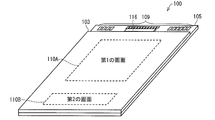
- FIG. 1 is a perspective view illustrating a schematic configuration of a display panel according to an embodiment of the present invention. It is a figure which shows the qualitative relationship between the arrangement pitch of the several unit circuit which concerns on a 1st row control circuit, and the width
- FIG. 2 is a perspective view showing a schematic configuration of the display panel 1 according to the present embodiment.
- the extending direction of the first row control line and the second row control line is described as the row direction
- the extending direction of the first column control line and the second column control line is described. Is described as the column direction.
- the first row control line and the second row control line may be extended in the horizontal direction or in the vertical direction. Needless to say.
- the display panel 1 is assumed to be a liquid crystal panel.
- the present embodiment is not limited to this.
- the first screen 10A includes two first row control circuits 13A and a first column control circuit 14A that control the first screen 10A, and a first counter electrode 2A.
- the first counter electrode 2A is electrically connected to the external terminal 9 of the element side substrate 5 via the first common transfer wiring 15A and the common transfer portions 20A to 20D.
- the common dislocation portions 20A to 20D are supplied with the potential from the counter electrode 2A through the common dislocation wiring 15A.
- the second screen 10B includes a second row control circuit 13B and a second column control circuit 14B for controlling the second screen 10B, and a second counter electrode 2B.
- the second counter electrode 2B is electrically connected to the external terminal 9 of the element side substrate 5 via the second common transition wiring 15B and the common transition portions 20E to 20H.
- a potential from the counter electrode 2B is applied to the common dislocation portions 20E to 20H via the common dislocation wiring 15B.
- Each of the common transition portions 20A to 20D and the counter electrode 2A, and each of the common dislocation portions 20E to 20H and the counter electrode 2B are electrically connected to each other via a conductive member contained in the sealing material 4.
- Each of the common transition portions 20A to 20D and the counter electrode 2A, and each of the common dislocation portions 20E to 20H and the counter electrode 2B can be made conductive via a conductive paste.
- the common dislocation portions 20B, 20C, 20E, and 20H are also close to each other. is there. Therefore, it is preferable to use a conductive member for conduction between the common transition portions 20A to 20D and the counter electrode 2A, and the common dislocation portions 20E to 20H and the counter electrode 2B.
- the first screen 10A and the second screen 10B are electrically independent, and if necessary, one operation can be stopped to reduce power consumption.
- high-resolution (for example, 4.23 type 540RGB ⁇ 960) transmissive color display is performed on the first screen 10A, and low-resolution (for example, 2.3 type) is displayed on the second screen 10B.
- 07 type 304 ⁇ 56) transflective black and white display that is, if the number of rows on the first screen (the number of first row control lines 11A) is m and the number of rows on the second screen (the number of second row control lines 11B) is n, then m> n. Are in a relationship. Therefore, the number of second row control lines 11B is smaller than the number of first row control lines 11A.
- FIG. 1 is an enlarged view of a part of the element-side substrate 5 of the display panel 1 according to the present embodiment.
- the element side substrate 5 of the display panel 1 includes two first row control circuits 13A, a second row control circuit 13B, a first column control circuit 14A, and a second column.
- a drive circuit such as the control circuit 14B and the external terminal 9 are monolithically arranged. These drive circuits and external terminals 9 are arranged in a frame area around the display area (the first screen 10A and the second screen 10B) in the display panel 1.
- the frame area is a non-display area and is an area where no image is displayed.
- the two first row control circuits 13A are respectively arranged in two frame regions extending in the row direction (that is, left and right edges on the paper surface) among the frame regions around the first screen 10A. Then, the plurality of first row control lines 11A are controlled from the left and right. Therefore, the first row control circuit 13A is arranged on two sides orthogonal to the side on which the external terminal 9 is arranged among the four sides constituting the frame region.
- the first column control circuit 14A is disposed in a frame region (that is, an upper edge portion on the paper surface) between the external terminal 9 and the first screen 10A. Accordingly, the first column control circuit 14A is arranged on the side where the external terminal 9 is arranged among the four sides constituting the frame region.
- the first column control circuit 14A controls the plurality of first column control lines 12A.
- the plurality of first storage capacitor lines 17A are for forming an auxiliary capacitor, are extended in the row direction, and are arranged between two adjacent first row control lines 11A. Yes.
- the second screen 10B includes a plurality of second row control lines 11B extending in the row direction (horizontal direction on the drawing) and a plurality of second column control lines 12B extending in the column direction (vertical direction on the drawing). And are provided.
- the plurality of second row control lines 11B and the plurality of second column control lines 12B are provided so as to cross each other in a matrix, and one second row control line 11B and one second column are provided.
- a region surrounded by the control line 12B is one pixel. That is, the area surrounded by the member number 30B in FIG. 1 is one pixel area.
- the second screen 10B has a configuration in which the above pixels are arranged in a matrix.
- the second row control circuit 13B is arranged in one of the two frame regions extending in the column direction (that is, the left and right edges on the paper surface) among the frame regions around the second screen 10B.
- the plurality of second row control lines 11B are controlled. Therefore, the second row control circuit 13B is arranged on one of the two sides where the two first row control circuits 13A are arranged among the four sides constituting the frame region.
- the second column control circuit 14B faces the first screen 10A through the second screen 10B among the frame regions around the second screen 10B and extends in the row direction (that is, the frame region (that is, the second screen 10B). , The lower edge on the paper surface). Therefore, the second column control circuit 14B is arranged on the side opposite to the side where the external terminal 9 is arranged among the four sides constituting the frame region.
- the second column control circuit 14B controls a plurality of second column control lines 12B.
- the individual display elements on the first screen 10A are formed in the vicinity of intersections of the plurality of first row control lines 11A and the plurality of first column control lines 12A, and include thin film transistors (not shown) and pixel electrodes (see FIG. And a first storage capacitor line 17A as basic components. That is, the display element is arranged for each subpixel.
- P_PIX1 is the pitch in the column direction of subpixels (that is, the arrangement pitch of the plurality of first row control lines 11A), which is a structural unit of the first screen 10A
- the pitch in the row direction that is, a plurality of pitches
- the arrangement pitch of the first column control lines 12A is 1/3 of P_PIX1. This is because the three subpixels of RGB constitute one pixel.
- the second screen 10B individual display elements are formed in the vicinity of intersections of the plurality of second row control lines 11B and the plurality of second column control lines 12B, and thin film transistors (not shown) and pixels are formed.
- An electrode (not shown) is included as a basic component. That is, the display element is arranged for each pixel.
- P_PIX2 is the pitch in the column direction of pixels (that is, the arrangement pitch of the plurality of second row control lines 11B), which is the constituent unit of the second screen 10B
- the pitch in the row direction that is, the plurality of first rows
- the arrangement pitch of the second row control lines 12B is also the same as P_PIX2.
- the second screen 10B uses a square pixel for monochrome display.
- the present invention is not necessarily limited to this, and the aspect ratio of the pixels may not be 1: 1. Therefore, for example, the aspect ratio of the pixels constituting the second screen 10B is not set to 1: 1, and the pixels of the structural unit of the second screen 10B may be sub-pixels as in the first screen 10A. .
- each display element of the first screen 10A includes a plurality of first row control lines 11A and a plurality of first column control lines 12A. It is formed near the intersection.
- Each display element has a thin film transistor (not shown), a pixel electrode (not shown), and a storage capacitor line 17A as basic components, and a dot inversion drive in which the first counter electrode 2A is applied with DC. It is the structure which performs.
- the second screen 10B is configured to be able to be driven using a so-called “pixel memory liquid crystal” in which each pixel includes a pixel memory for storing image data supplied from an IC driver.
- Each display element of the second screen 10B is formed in the vicinity of the intersection of the plurality of second row control lines 11B and the plurality of second column control lines 12B.
- Each display element has an SRAM (not shown), and the second counter electrode 2B is configured to perform AC-driven frame inversion driving. Therefore, each display element on the second screen 10B applies a binary voltage to the power line and the liquid crystal for driving the SRAM in addition to the second row control line 11B and the second column control line 12B.
- Power supply line and a plurality of thin film transistors (not shown). It should be noted that circuits (timing generator, VCOM circuit, etc.) relating to driving of the second screen 10B may be monolithically incorporated in the element side substrate 5.
- the two first row control circuits 13A have two frame regions extending in the column direction among the frame regions around the first screen 10A (that is, the paper surface). They are monolithically arranged on the left and right edges).
- the first row control circuit 13A drives m first row control lines 11A (for example, 960 in the case of resolution 540RGB ⁇ 960) from the left and right. This configuration is suitable for driving a high-definition display and contributes to the reduction of crosstalk (also called shadowing).
- a control line 25A (including a power supply line and a clock signal line) is drawn from the first row control circuit 13A to the external terminal 9 through a frame area in the vicinity of the external terminal 9.
- the display panel 1 shown in FIG. 1 includes a circuit 7 such as a buffer circuit or a protection circuit at the end of the first row control circuit 13A on the external terminal 109 side. These circuits 7 may be provided as necessary and are not necessarily provided.
- the first row control circuit 13A is configured by repeatedly arranging unit circuits 13a (first row unit circuits) including a shift register and an output circuit in a column direction at a predetermined pitch.
- Each unit circuit 13a may include a level shifter as necessary.
- the arrangement pitch of the plurality of first row control lines 11A is P_PIX1
- the arrangement pitch of the plurality of unit circuits 13a of the first row control circuit 13A is P_D1
- P_PIX1> P_D1 A plurality of first row control lines 11A and a plurality of unit circuits 13a are arranged so that the above relationship is established.
- the length of the first row control circuit 13A (dimension in the column direction (vertical direction in the drawing)) can be reduced.
- FIG. 3 is a diagram showing a qualitative relationship between the arrangement pitch of the plurality of unit circuits 13a and the width of each unit circuit 13a.
- a general unit circuit is rarely arranged in L / S (line / space) which is permitted in design, and it is in the direction of a thin film transistor, the direction of wiring, and the arrangement of various components. In many cases, it includes some free space generated for the reasons described above.
- a unit circuit having a width B is formed as a result of arranging the arrangement pitch P_PIX1 of the plurality of first row control lines at the pitch A and arranging the plurality of unit circuits at the pitch A.
- the arrangement pitch of the plurality of unit circuits and the width of each unit circuit are in a discrete relationship with each other.
- the width of each unit circuit 13a is equal to the width of each unit circuit 13a when the plurality of first row control lines 11A and the plurality of unit circuits 13a are arranged at the same arrangement pitch. It is preferable that the arrangement pitch of the plurality of unit circuits 13a is smaller than the arrangement pitch of the plurality of first row control lines 11A. According to this, even if the arrangement pitch of the plurality of unit circuits 13a is reduced, the width of each unit circuit 13a does not change because of the potential nature of the unit circuit 13a, and therefore the first row control circuit 13A.
- the frame area provided with is never narrowed. That is, even if the arrangement pitch of the plurality of unit circuits 13a is reduced, in order to increase the width (dimension in the row direction (horizontal direction)) of the frame area in which the first row control circuit 13A is provided, There is no need to increase the external dimensions of the display panel 1.
- the width of the unit circuit 13a not being unreasonably large, the dimensions of the frame regions located on the left and right of the first screen 10A (that is, the first orthogonal to the side on which the external terminal 9 is disposed,
- the shortest distance from the end of the screen 10A to the end of the substrate 3 parallel to the end is a, and the dimensions of the frame regions located on the left and right of the second screen 10B (external terminals 9 are arranged)
- b is the shortest distance from the end of the second screen 10B, which is perpendicular to the edge of the second screen 10B, to the end of the substrate 3 parallel to the end, and a is approximately equal to b (a ⁇ b).
- a display panel 1 is obtained. Therefore, it is convenient for incorporating the display panel 1 into an electronic device.
- the diagonal size of the second screen 10B can be increased without changing the horizontal width (dimension in the horizontal direction of the drawing) of the display panel 1. Therefore, it is convenient when it is desired to emphasize the diagonal size of the second screen 10B. Note that it is preferable to set the optimum diagonal size in consideration of incorporation into an electronic device and accuracy during incorporation into the electronic device.
- the first row control line near the external terminal 9 is used.
- 11A is arranged to be a longer-distance diagonal wiring.
- the first row control line 11A near the second screen 10B is arranged to be a diagonal wiring with a shorter distance. That is, the first row control lines 11A closer to the second screen 10B are arranged to be substantially horizontal lines (parallel to the first row control lines 11A).
- the arrangement pitch of the plurality of unit circuits 13a is reduced, the end on the second row control circuit 13B side in the first row control circuit 13A, and the second screen 10B in the first screen 10A.
- the side end is arranged in a substantially straight line.
- the position of the end on the external terminal 9 side in the first row control circuit 13A can be moved to the second row control circuit 13B side.
- the circuit 7 including the buffer circuit or the protection circuit 7 can be moved to the second screen 10B side, the frame region on the external terminal 9 side, more specifically, the frame region on the external terminal 9 side. An empty area is generated at the corner.
- the arrangement pitch of the plurality of unit circuits 13a is made smaller than that of the plurality of first row control lines 11A, and the second row control circuit 13B side in the first row control circuit 13A.
- the outer dimensions of the display panel 1 can be kept small, the merchantability of the display device or electronic device using the display panel 1 can be improved.
- the frame region is reduced, a plurality of display panels 1 can be arranged on the substrate. As a result, an increase in manufacturing cost of the display panel 1 can be suppressed.
- the first column control circuit 14A of the first screen 10A is monolithically formed in the frame region (that is, the upper edge on the paper surface) between the external terminal 9 and the first screen 10A on the element side substrate 5.
- the first column control circuit 14A drives a plurality of first column control lines 12A (for example, resolution 540 ⁇ 3 in the case of resolution 540RGB ⁇ 960).
- the first column control circuit 14A is connected to a driver IC externally attached to the display panel 1 through the video signal line 8.
- the first column control circuit 14A is configured by repeatedly arranging unit circuits 14a (first column unit circuits) including a switch circuit in a row direction at a predetermined pitch.
- Each unit circuit 14a may include a level shifter as necessary.
- a video signal from the driver IC is sent to each unit circuit 14a of the first column control circuit 14A via the video signal line 8.
- the first column control circuit 14A receives the input from one video signal line 8 as the first of the red (R), green (G), and blue (B) sub-pixels constituting one pixel.
- a control line 25A (including a power supply line and a clock signal line) is drawn from the first column control circuit 14A to the external terminal 9 through a frame area in the vicinity of the external terminal 9. Therefore, protection circuits 6 are disposed at both ends of the first column control circuit 14A on the first row control circuit 13A side in order to protect the control lines 25A drawn from the first column control circuit 14A from static electricity. It may be. By the way, since the protection circuit 6 that protrudes in the row direction from the first column control circuit 14A may interfere with the first row control circuit 13A, the outer dimensions of the display panel 1 are increased in order to avoid the interference. May take action.
- the arrangement pitch of the plurality of unit circuits 14a is slightly smaller than the arrangement pitch of the plurality of first column control lines 12A in order to avoid increasing the outer dimensions of the display panel 1. It is preferable to do.
- the plurality of first column control lines 12A drawn between the first column control circuit 14A and the first screen 10A are fan-shaped diagonal wirings.
- the second row control circuit 13B includes two frame regions extending in the column direction among the frame regions around the second screen 10B (that is, on the paper surface). It is arranged monolithically on either of the left and right edges.
- the second row control circuit 13B drives n (for example, 56 in the case of a resolution of 304 ⁇ 56) second row control lines 11B.
- n for example, 56 in the case of a resolution of 304 ⁇ 56
- a control line 25B (including a power supply line and a clock signal line) is drawn from the second row control circuit 13B to the external terminal 9 so as to bypass the first row control circuit 13A.
- the second row control circuit 13B is configured by repeatedly arranging unit circuits 13b (second row unit circuits) including a shift register and an output circuit in a column direction at a predetermined pitch. Each unit circuit 13b may include a level shifter as necessary.
- the arrangement pitch of the plurality of second row control lines 11B on the second screen 10B is P_PIX2, and the arrangement pitch of the plurality of unit circuits 13b of the second row control circuit 13B is P_D2.
- an empty area can be created in the frame area. it is conceivable that.
- the arrangement pitch of the plurality of unit circuits 13b is preferably equal to the arrangement pitch of the plurality of second row control lines 11B.
- the second column control circuit 14B of the second screen 10B faces the first screen 10A via the second screen 10B in the frame area around the second screen 10B in the element-side substrate 5.
- the frame region is monolithically arranged in a frame region extending in the row direction (that is, a lower frame region on the paper surface).
- the second column control circuit 14B controls a plurality of second column control lines 12B (for example, 304 in the case of 304 ⁇ 56 resolution).
- a control line 25B (including a power supply line and a clock signal line) passes through the boundary region between the first screen 10A and the second screen 10B, and passes through the first row control circuit 14B. It is pulled out to the external terminal 9 so as to bypass 13A.
- the control line 25B includes a power line for driving the SRAM provided in each display element of the second screen 10B and a power line for applying a binary voltage to the liquid crystal. These power supply lines traverse and traverse the second screen 10B.
- the second column control circuit 14B serves as a binary driver for sending a binary signal (display ON / OFF) to each display element of the second screen 10B. Therefore, on the second screen 10B, the voltage for driving the liquid crystal is supplied from the power supply line for applying a binary voltage to the liquid crystal via the SRAM.
- the second column control circuit 14B is configured by repeatedly arranging unit circuits 14b including a shift register and an output circuit in a row direction at a predetermined pitch.
- Each unit circuit 14b may include a level shifter as necessary.
- the boundary region between the first screen 10A and the second screen 10B is separated by a predetermined distance Q (for example, about 1 mm). Between the left and right frame regions (edges) on the paper surface through the wiring (for example, the first storage capacitor line 17A and the first common dislocation wiring 15A) for driving the first screen 10A in this boundary region It is good to cross. As a result, it becomes possible to increase the redundancy of the wiring and to improve the uniformity of the display on the first screen 10A.
- wiring for driving the second screen 10B may be passed through the boundary area. For example, by passing the power supply line necessary for driving the SRAM through the boundary region, it is possible to route the power supply line from the outermost periphery of the display panel 1 toward the inside of the display panel 1 at a short distance.
- the end on the second screen 10B side in the first screen 10A and the end on the second row control circuit 13B side in the first row control circuit 13A are arranged in a substantially straight line.
- the end on the first screen 10A side in the second screen 10B and the end on the first row control circuit 13A side in the second row control circuit 13B are arranged in a substantially straight line.
- the separation distance between the first row control circuit 13A and the second row control circuit 13B becomes substantially equal to the separation distance Q between the first screen 10A and the second screen 10B.
- the wiring for driving the first screen 10A and the wiring for driving the second screen 10B can be surely passed through the boundary region between the first screen 10A and the second screen 10B. It becomes possible.
- the configuration in which the display panel 1 includes the two first row control circuits 13A has been described, but the configuration is not necessarily limited thereto. Therefore, the first row control circuit 13A only needs to be arranged on at least one of the two sides adjacent to the side where the external terminal 9 is arranged among the four sides constituting the frame region.
- the second row control circuit 13B is arranged on the side where the first row control circuit 13A is arranged among the four sides constituting the frame region.
- the display medium may be a display medium having electro-optical characteristics, and may be, for example, electroluminescence (EL), plasma, or electrochromic.
- EL electroluminescence
- the present invention can be applied to display panels of various display devices using various display media such as liquid crystal display devices, EL display devices, and electrophoretic display devices.
- a display panel having a relationship of m> n where m is the number of lines on the first screen and n is the number of lines on the second screen, and the four of the four sides constituting the frame area of the display panel
- Any display panel in which an external terminal is provided only on one side can be applied to the present invention.
- the display panel according to this embodiment can be used for an electronic device including the display device as a display unit.
- electronic devices include cellular phones, PDAs (Personal Digital Assistants), DVD (Digital Versatile Disk) players, mobile game devices, notebook PCs (Personal Computers), PC monitors, and television receivers. Etc.
- the electronic device according to the present embodiment includes the display device itself. That is, the electronic device according to the present embodiment (that is, the electronic device including the display panel according to the present embodiment) may be a display device such as a liquid crystal display device, and these display devices are used as a display unit. It may be a device provided.
- the display panel according to the present invention has the above-mentioned 4. It is sufficient to have at least the configuration described in 5. ⁇ 8. It is not always necessary to have the configuration described in. Therefore, the above 5. ⁇ 8.
- the configuration described in 1 is to be understood as a configuration that can be appropriately added to the display panel according to the present invention. In other words, the above 5.
- ⁇ 8. The configuration described in is a modification of the display panel according to the present invention.
- the array pitch of the plurality of second row control lines is substantially equal to the array pitch of the plurality of second row unit circuits. It is a feature.
- an empty area can be created in the frame area by making the arrangement pitch of the plurality of second row unit circuits smaller than the arrangement pitch of the plurality of second row control lines. It is done. However, since the number of rows on the second screen (the number of second row control lines) is small, the entire second row control circuit occupies even if the arrangement pitch of the plurality of second row unit circuits is somewhat reduced. It is not possible to create an empty area as the area is reduced. Therefore, on the second screen, the arrangement pitch of the plurality of second row unit circuits is preferably equal to the arrangement pitch of the plurality of second row control lines.
- an end portion on the first screen side in the second screen, and an end portion on the first row control circuit side in the second row control circuit. Is characterized by being arranged in a substantially straight line.
- the separation distance between the first row control circuit and the second row control circuit is substantially equal to the separation distance between the first screen and the second screen.
- the control line for controlling the second screen can be surely passed through the boundary area between the first screen and the second screen.
- the first column unit provided for each of the first column control lines and arranged side by side in a direction orthogonal to the plurality of first column control lines.
- a plurality of circuits further including a first column control circuit disposed on the side where the external terminal is disposed, wherein an arrangement pitch of the plurality of first column unit circuits is the plurality of first columns It is characterized by being smaller than the arrangement pitch of the column control lines.
- the arrangement pitch of the plurality of first column unit circuits is slightly smaller than the arrangement pitch of the plurality of first column control lines.
- the end of the substrate is parallel to the end from the end of the first screen, which is orthogonal to the side where the external terminal is disposed. Is approximately equal to the shortest distance from the edge of the second screen, which is orthogonal to the side where the external terminal is disposed, to the edge of the substrate, which is parallel to the edge. It is characterized by being.
- the above configuration is convenient for incorporating the display panel into an electronic device.
- the present invention can be applied to a display panel using, for example, electroluminescence (EL), plasma, electrochromic, or the like as a display medium.
- the liquid crystal display device including the display panel according to the present invention, EL display The present invention can be applied to various display devices such as a device or an electrophoretic display device.
- the display panel according to the present invention can also be used in an electronic device provided with the above display device as a display unit. Examples of such an electronic device include a mobile phone and a PDA (Personal Digital Assistant; A terminal), a DVD (Digital Versatile Disk) player, a mobile game machine, a notebook PC (Personal Computer), a PC monitor, a television receiver, and the like.
Landscapes
- Physics & Mathematics (AREA)
- Engineering & Computer Science (AREA)
- General Physics & Mathematics (AREA)
- Chemical & Material Sciences (AREA)
- Crystallography & Structural Chemistry (AREA)
- Nonlinear Science (AREA)
- Computer Hardware Design (AREA)
- Theoretical Computer Science (AREA)
- Mathematical Physics (AREA)
- Optics & Photonics (AREA)
- Devices For Indicating Variable Information By Combining Individual Elements (AREA)
Abstract
本発明に係る表示パネル(1)においては、第1の画面(10A)における複数の第1の行制御線(11A)の配列ピッチをP_PIX1とし、第1の行制御回路(13A)の複数の単位回路(13a)の配列ピッチをP_D1とすると、P_PIX1>P_D1の関係が成立する。さらに、第1の行制御回路(13A)と第1の画面(10A)との間に引き出される複数の第1の行制御線(11A)のうち、外部端子(9)寄りのものは長距離の斜め配線とし、第2の画面(10B)寄りのものは短距離の斜め配線としている。
Description
各種の駆動回路が基板上にモノリシック化されて形成されている表示パネル、および、該表示パネルを備えた表示装置、ならびに、該表示パネルを備えた電子機器に関する。
液晶パネルに代表される表示パネルは一般的に実用化されており、様々な電子機器、特に携帯電子機器に搭載されている。近年ではより一層の小型化を図るために、多結晶シリコンを利用した各種の駆動回路を基板上にモノリシックに形成した表示パネルが製品化されている。さらには、多様な回路を1枚の基板上に形成可能であることを利用して、1枚の表示パネルに2つの表示画面を備えた表示パネルも製品化されている。
例えば、特許文献1には2つの表示画面を備えた表示パネルが開示されている。このような表示パネルの構成について、図4および図5を参照して説明する。図4および図5は、表示パネルの概略構成を示す斜視図である。
図4に図示すように、表示パネル100は、ガラスからなる対向側基板103と素子側基板105とが貼り合せられた構成をしている。この表示パネル100では、該表示パネル100を平面視したとき(すなわち、表示パネル100を上方から見たとき)に、外部端子109と、第1の画面110Aと、第2の画面110Bとがこの順で並んでいる。この際、外部端子109は、第1の画面110Aおよび第2の画面110Bを取り囲む額縁領域(縁部)のうち、第1の画面110Aを介して第2の画面110Bと対向する額縁領域に設けられている。したがって、外部端子109は、額縁領域を構成する四辺のうち、1つの辺にのみ設けられている。このように、額縁領域の1つの辺のみに外部端子109が配置された構成は「3辺フリー構造」と呼ばれ、電気機器への組み込みの扱いが容易になる利点があることから、近年特に好まれている構成である。
表示パネル100では、第1の画面110Aには高解像度(例えば、640RGB×960)の透過型のカラー表示を行い、第2の画面110Bには低解像度(例えば、208×40)の半透過型の白黒表示を行っている。このように、表示パネル100では、第1の画面110Aおよび第2の画面110Bを備えていることから、表示したい内容とその利用場面とに応じた使い分けが可能な構成とされている。
図5に示すように、第1の画面110Aは、第1の画面110Aを制御する2つの第1の行制御回路113Aおよび第1の列制御回路114A、ならびに、第1の対向電極102Aを備えている。一方、第2の画面110Bは、第2の画面110Bを制御する第2の行制御回路113Bおよび第2の列制御回路114B、ならびに、第2の対向電極102Bを備えている。ここで、第1の画面110Aと第2の画面110Bとは電気的に独立しており、必要であれば一方の動作を停止させて消費電力を削減することができる。
第1の画面110Aにおいては、個々の表示素子は複数の第1の行制御線111Aと複数の第1の列制御線112Aとの交点付近に形成され、薄膜トランジスタ(図示せず)および画素電極(図示せず)を基本構成物として有している。同様に、第2の画面110Bにおいては、複数の第2の行制御線111Bと複数の第2の列制御線112Bとの交点付近に個々の表示素子は形成され、薄膜トランジスタ(図示せず)および画素電極(図示せず)を基本構成物として有している。ここで、2つの第1の行制御回路113Aは、第1の画面110Aの周囲の額縁領域のうち、複数の第1の列制御線112Aと平行な2つの額縁領域(すなわち、左右の縁部)にそれぞれ配置され、複数の第1の行制御線111A(ゲートバスライン)を左右から制御する。なお、第1の行制御回路113Aは、外部端子109側の端部にバッファ回路または保護回路等の回路107を備えている場合もある。また、第1の列制御回路114Aは、外部端子109と第1の画面110Aとの間の額縁領域に配置され、複数の第1の列制御線112A(ソースバスライン)を制御する。なお、第1の列制御回路114Aは、第1の行制御回路113A側の両端部にそれぞれ保護回路6が配置されていてもよい。
なお、第1の列制御回路114Aは、ドライバIC116からのビデオ信号を、1つの画素を構成する赤色(R)、緑色(G)、および、青色(B)の各副画素の第1の列制御線112Aに振り分ける簡単なRGBスイッチの役割を担う。これによって、ドライバIC116からの出力配線の数を減らすことが可能になり、少ないドライバIC116であっても高精細な表示が可能となる。
第1の対向電極102Aは、第1のコモン転移用配線115Aおよびコモン転移部120A~120Dを介して素子側基板105の外部端子109に電気的に接続されている。図5では、第1のコモン転移用配線115Aに接続されているコモン転移部は4箇所(A~D)あり、これらは第1の画面110Aの4隅近傍に形成されている。一方、第2の対向電極102Bは、第2のコモン転移用配線115Bおよびコモン転移部120E~120Hを介して素子側基板105の外部端子109に電気的に接続されている。図5では、第2のコモン転移用配線115Bに接続されているコモン転移部は4箇所(E~H)あり、これらは第2の画面110Bの4隅近傍に形成されている。
各コモン転移部120A~120Dおよび対向電極102A、ならびに、各コモン転位部120E~120Hおよび対向電極102Bは、それぞれシール材104に含有されている導電部材または導電性のペーストを介して電気的に接続されている。第2の画面110Bの駆動に必要な制御線(電源線およびクロック信号線等を含む)は、表示パネル100の第1の行制御回路113Aを迂回するように表示パネル100の額縁領域を通り抜けて、表示パネル100に設けられた外部端子109に引き出されている。
図5に示す表示パネル100では、外部端子109と、第1の画面110Aと、第2の画面110Bとがこの順で並んでいるため、第2の画面110Bの制御線は、第1の行制御回路113Aの傍らを迂回して該外部端子109に引き出されている。このため、表示パネル100における外部端子109側の額縁領域の隅部分に配線レイアウトが集中してしまう。この結果、表示パネル100の外部端子109側の額縁領域が大きくなり、表示パネル100を組み込んだ電子機器の商品性の魅力が乏しくなってしまう。
そこで、本発明は上記の課題に鑑みてなされたものであり、その目的は、表示パネルにおける外部端子側の額縁領域の隅部分に配線レイアウトが集中することに起因して、表示パネルにおける外部端子側の額縁領域の隅部分が大きくなることを防ぐことができる表示パネル、および、該表示パネルを備えた表示装置、ならびに、該表示パネルを備えた電子機器を提供することにある。
本発明の一態様に係る表示パネルは、上記の課題を解決するために、表示領域と、当該表示領域を取り囲む非表示領域である額縁領域とを有する基板を備えた表示パネルであって、上記額縁領域を構成する四辺のうちいずれか1つの辺のみに配置されている外部端子と、上記外部端子が形成されている辺と平行に配置された複数の第1の行制御線と、該複数の第1の行制御線と交差する複数の第1の列制御線とを含み、上記表示領域内に設けられている第1の画面と、上記複数の第1の行制御線よりも少なくかつ上記複数の第1の行制御線と平行に配置されている複数の第2の行制御線と、該複数の第2の行制御線と交差する複数の第2の列制御線とを含み、上記表示領域内において上記第1の画面を介して上記外部端子と対向する位置に設けられている第2の画面と、上記第1の行制御線ごとに設けられかつ上記複数の第1の行制御線と直交する方向に並んで配置されている第1の行単位回路を複数含み、上記外部端子が配置されている上記辺と直交する上記辺に配置されている第1の行制御回路と、上記第2の行制御線ごとに設けられかつ上記複数の第2の行制御線と直交する方向に並んで配置された第2の行単位回路を複数含み、上記第1の行制御回路が配置されている上記辺に配置されている第2の行制御回路と、上記外部端子から上記第2の画面まで上記第1の行制御回路を迂回するように上記額縁領域内を通って延伸している、上記第2の画面を制御するための制御線とをさらに備えており、上記複数の第1の行単位回路の配列ピッチは、上記複数の第1の行制御線の配列ピッチよりも小さく、上記第1の画面における上記第2の画面側の端部と、上記第1の行制御回路における上記第2の行制御回路側の端部とは、略一直線上に並んでいることを特徴としている。
上記の構成にすることによって、第1の行制御回路の長さ(列方向の寸法)を小さくすることができる。結果、第1の画面の周囲の額縁領域に空き領域を生み出すことができる。
さらに、第1の行制御回路における第2の行制御回路側の端部と、第1の画面における第2の画面側の端部とが略一直線上に並ぶように構成している。これによって、第1の行制御回路における外部端子側の端部の位置を、第2の行制御回路側に移動することができる。結果、外部端子側の額縁領域、より具体的には、外部端子側の額縁領域の隅部分に空き領域が生じる。
したがって、複数の第1の行制御線よりも複数の第1の行単位回路の配列ピッチを小さくすると共に、第1の行制御回路における第2の行制御回路側の端部と第1の画面における第2の画面側の端部とを略一直線上に並べていることによって、表示パネルの隅部分に空き領域を生み出すことができる。この生じた空き領域を利用して、制御線(電源線およびクロック信号線等を含む)を外部端子まで引き出すことができる。すなわち、外部端子側の額縁領域の隅部分に配線レイアウトが集中してしまうがために、外部端子側の額縁領域を大きくしなくても、第2の画面の制御線を外部端子まで引き出すことができる。
また、本発明の一態様に係る表示装置は、上述した表示パネルを備えていることを特徴としている。
上記の構成によれば、外部端子側の額縁領域の隅部分に配線レイアウトが集中してしまうがために、外部端子側の額縁領域を大きくしなくても、第2の画面を制御するための制御線を外部端子まで引き出すことができる。結果、商品性の高い表示パネルを提供することができる。
また、本発明の一態様に係る電子機器は、上述した表示パネルを備えていることを特徴としている。
上記の構成によれば、外部端子側の額縁領域の隅部分に配線レイアウトが集中してしまうがために、外部端子側の額縁領域を大きくしなくても、第2の画面を制御するための制御線を外部端子まで引き出すことができる。結果、商品性の高い電子機器を提供することができる。
本発明の他の目的、特徴、および優れた点は、以下に示す記載によって十分分かるであろう。また、本発明の利点は、添付図面を参照した次の説明で明白になるであろう。
本発明によれば、外部端子側の額縁領域の隅部分に配線レイアウトが集中してしまうがために、外部端子側の額縁領域を大きくしなくても、第2の画面を制御するための制御線を外部端子まで引き出すことができる。結果、表示パネルを使った表示装置あるいは電子機器の商品性を高めることができる。また、額縁領域が縮小されたことにより、表示パネルを基板上に複数配置することができる結果、表示パネルの製造コストの増加を抑制することができる。
本発明の実施の形態について図面を参照して説明すれば、以下の通りである。
(1.表示パネルの構成)
まず、本実施の形態に係る表示パネルについて、図2を参照して説明する。図2は、本実施の形態に係る表示パネル1の概略構成を示す斜視図である。なお、説明の便宜上、以下の説明では、第1の行制御線および第2の行制御線の延伸方向を行方向として説明し、第1の列制御線および第2の列制御線の延伸方向を列方向として説明する。ただし、本実施の形態に係る表示パネル1の使用に際し、上記の第1の行制御線および第2の行制御線が横方向に延伸されていても、縦方向に延伸されていてもよいことは言うまでもない。ところで、以下では、表示パネル1が液晶パネルである場合を想定して説明するが、本実施の形態はこれに限定されるわけではない。
まず、本実施の形態に係る表示パネルについて、図2を参照して説明する。図2は、本実施の形態に係る表示パネル1の概略構成を示す斜視図である。なお、説明の便宜上、以下の説明では、第1の行制御線および第2の行制御線の延伸方向を行方向として説明し、第1の列制御線および第2の列制御線の延伸方向を列方向として説明する。ただし、本実施の形態に係る表示パネル1の使用に際し、上記の第1の行制御線および第2の行制御線が横方向に延伸されていても、縦方向に延伸されていてもよいことは言うまでもない。ところで、以下では、表示パネル1が液晶パネルである場合を想定して説明するが、本実施の形態はこれに限定されるわけではない。
図2に示すように、本実施の形態に係る表示パネル1は、従来の表示パネルと同じく、ガラスからなる対向側基板3および素子側基板5それぞれの表面に形成された構成物が互いに向かい合うようにして、シール材4を介して両基板を貼り合せた構成をとる。また、表示パネル1を平面視したとき(すなわち、表示パネル1を上方から見たとき)に、該表示パネル1の外部端子9と、第1の画面10Aと、第2の画面10Bとがこの順で並んでいる。この際、外部端子9は、第1の画面10Aおよび第2の画面10Bを取り囲む額縁領域(縁部)のうち、第1の画面10Aを介して第2の画面10Bと対向し、行方向に延伸する額縁領域(すなわち、紙面上の上部の縁部)に設けられている。したがって、表示パネル1は、額縁領域を構成する四辺のうち、1つの辺にのみ外部端子9を設けている、いわゆる「3辺フリー構造」である。
第1の画面10Aは、第1の画面10Aを制御する2つの第1の行制御回路13Aおよび第1の列制御回路14A、ならびに、第1の対向電極2Aを備えている。第1の対向電極2Aは、第1のコモン転移用配線15Aおよびコモン転移部20A~20Dを介して素子側基板5の外部端子9に電気的に接続されている。図2では、第1のコモン転移用配線15Aに接続されているコモン転移部は4箇所(A~D)あり、これらは第1の画面10Aの4隅近傍に形成されている。これらのコモン転位部20A~20Dには、対向電極2Aからの電位がコモン転位用配線15Aを介して与えられる。
一方、第2の画面10Bは、第2の画面10Bを制御する第2の行制御回路13Bおよび第2の列制御回路14B、ならびに、第2の対向電極2Bを備えている。第2の対向電極2Bは、第2のコモン転移用配線15Bおよびコモン転移部20E~20Hを介して素子側基板5の外部端子9に電気的に接続されている。図2では、第2のコモン転移用配線15Bに接続されているコモン転移部は4箇所(E~H)あり、これらは第2の画面10Bの4隅近傍に形成されている。これらのコモン転位部20E~20Hには、対向電極2Bからの電位がコモン転位用配線15Bを介して与えられる。
各コモン転移部20A~20Dおよび対向電極2A、ならびに、各コモン転位部20E~20Hおよび対向電極2Bは、それぞれシール材4に含有されている導電部材を介して電気的に接続されている。なお、各コモン転移部20A~20Dおよび対向電極2A、ならびに、各コモン転位部20E~20Hおよび対向電極2Bは、それぞれ導電性ペーストを介して導通させることは可能である。しかしながら、第1の画面10Aと第2の画面10Bとが近接していることからコモン転位部20B,20C,20E,20Hも互いに近接しているため、導電性ペーストの塗布ミスにより短絡する虞がある。そのため、各コモン転移部20A~20Dおよび対向電極2A、ならびに、各コモン転位部20E~20Hおよび対向電極2Bの導通には、導電部材を用いるのが好ましい。
ここで、第1の画面10Aと第2の画面10Bとは電気的に独立しており、必要であれば一方の動作を停止させて消費電力を削減することができる。本実施の形態では、第1の画面10Aには高解像度(例えば、4.23型の540RGB×960)の透過型のカラー表示を行い、第2の画面10Bには低解像度(例えば、2.07型の304×56)の半透過型の白黒表示を行う。つまり、第1の画面の行数(第1の行制御線11Aの数)をmとし、第2の画面の行数(第2の行制御線11Bの数)をnとすると、m>nの関係にある。したがって、第2の行制御線11Bの数は、第1の行制御線11Aの数よりも少ない。
(2.画面の構成)
以下では、表示パネル1の画面構成について、図1を参照して説明する。図1は、本実施の形態に係る表示パネル1の素子側基板5の一部を拡大した図である。
以下では、表示パネル1の画面構成について、図1を参照して説明する。図1は、本実施の形態に係る表示パネル1の素子側基板5の一部を拡大した図である。
図1に示すように、表示パネル1の素子側基板5には、2つの第1の行制御回路13A、第2の行制御回路13B、第1の列制御回路14A、および、第2の列制御回路14B等の駆動回路と、外部端子9とがモノリシックに配置されている。これらの駆動回路および外部端子9は、表示パネル1における表示領域(第1の画面10Aおよび第2の画面10B)の周辺の額縁領域に配されている。ここで、額縁領域とは非表示領域であり、画像が表示されない領域である。
表示パネル1の素子側基板5において、第1の画面10Aには、複数の第1の行制御線11Aと、複数の第1の列制御線12Aと、複数の第1の蓄積容量線17Aとが備えられている。複数の第1の行制御線11A(ゲートバスライン)は行方向(紙面水平方向)に延伸しており、複数の第1の列制御線12A(ソースバスライン)は列方向(紙面鉛直方向)に延伸している。複数の第1の行制御線11Aと複数の第1の列制御線12Aとは、マトリクス状に互いに交差して設けられており、1つの第1の行制御線11Aと1つの第1の列制御線12Aとによって囲まれた領域が1つの副画素である。すなわち、図1中の部材番号30Aによって囲まれた領域が1つの副画素領域である。第1の画面10Aは、各画素を構成する副画素をマトリクス状に配した構成を有している。
ここで、2つの第1の行制御回路13Aは、第1の画面10Aの周囲の額縁領域のうち、行方向に延伸する2つの額縁領域(すなわち、紙面上の左右の縁部)にそれぞれ配置され、複数の第1の行制御線11Aを左右から制御する。したがって、額縁領域を構成する四辺のうち、外部端子9が配置されている辺に直交する2つの辺に、第1の行制御回路13Aは配置されている。一方、第1の列制御回路14Aは、外部端子9と第1の画面10Aとの間の額縁領域(すなわち、紙面上の上部の縁部)に配置されている。したがって、額縁領域を構成する四辺のうち、外部端子9が配置されている辺に、第1の列制御回路14Aは配置されている。該第1の列制御回路14Aは、複数の第1の列制御線12Aを制御する。なお、複数の第1の蓄積容量線17Aは、補助容量を形成するためのものであり、行方向に延伸して設けられ、隣り合う2つの第1の行制御線11Aの間に配置されている。
一方、第2の画面10Bには、行方向(紙面水平方向)に延伸する複数の第2の行制御線11Bと、列方向(紙面鉛直方向)に延伸する複数の第2の列制御線12Bとが備えられている。複数の第2の行制御線11Bと複数の第2の列制御線12Bとは、マトリクス状に互いに交差して設けられており、1つの第2の行制御線11Bと1つの第2の列制御線12Bとによって囲まれた領域が1つの画素である。すなわち、図1中の部材番号30Bによって囲まれた領域が1つの画素領域である。第2の画面10Bは、上記の画素をマトリクス状に配した構成を有している。
ここで、第2の行制御回路13Bは、第2の画面10Bの周囲の額縁領域のうち、列方向に延伸する2つの額縁領域(すなわち、紙面上の左右の縁部)のいずれかに配置され、複数の第2の行制御線11Bを制御する。したがって、額縁領域を構成する四辺のうち、2つの第1の行制御回路13Aが配置されている二辺のいずれかに、第2の行制御回路13Bは配置されている。一方、第2の列制御回路14Bは、第2の画面10Bの周囲の額縁領域のうち、第2の画面10Bを介して第1の画面10Aと対向し、行方向に延伸する額縁領域(すなわち、紙面上の下部の縁部)に配置されている。したがって、額縁領域を構成する四辺のうち、外部端子9が配置されている辺に対向する辺に、第2の列制御回路14Bは配置されている。該第2の列制御回路14Bは、複数の第2の列制御線12Bを制御する。
第1の画面10Aにおける個々の表示素子は、複数の第1の行制御線11Aと複数の第1の列制御線12Aとの交点付近に形成され、薄膜トランジスタ(図示せず)と画素電極(図示せず)と第1の蓄積容量線17Aとを基本構成物として有している。すなわち、副画素ごとに、上記の表示素子が配置されている。
各副画素には、各画素電極に対応して赤色(R)、緑色(G)および青色(B)のいずれか1色の図示しないカラーフィルタが配されている。以下、赤色のカラーフィルタ、緑色のカラーフィルタ、および、青色のカラーフィルタを備えた副画素を、それぞれ赤色(R)の副画素、緑色(G)の副画素、青色(B)の副画素と称す。第1の画面10Aでは、RGBの3つの副画素が、行方向あるいは列方向に配列されている。このRGBの3つの副画素からなる副画素群が、カラー表示を行うための最小構成単位の画素(3原色用画素)である。すなわち、1つの画素は、RGBの3つの副画素で構成されている。
ここで、第1の画面10Aの構成単位である副画素の列方向のピッチ(すなわち、複数の第1の行制御線11Aの配列ピッチ)をP_PIX1とすると、行方向のピッチ(すなわち、複数の第1の列制御線12Aの配列ピッチ)はP_PIX1の1/3となる。これは、RGBの3つの副画素が1つの画素を構成しているためである。
一方、第2の画面10Bにおいては、複数の第2の行制御線11Bと複数の第2の列制御線12Bとの交点付近に個々の表示素子が形成され、薄膜トランジスタ(図示せず)と画素電極(図示せず)とを基本構成物として有している。すなわち、画素ごとに、上記の表示素子が配置されている。
ここで、第2の画面10Bの構成単位である画素の列方向のピッチ(すなわち、複数の第2の行制御線11Bの配列ピッチ)をP_PIX2とすると、行方向のピッチ(すなわち、複数の第2の行制御線12Bの配列ピッチ)もP_PIX2と同じになる。これは、第2の画面10Bでは白黒表示を行うため、正方画素にしているからである。しかし、必ずしもこれに限定されるわけではなく、画素の縦横のアスペクトは1:1でなくてもよい。したがって、例えば、第2の画面10Bを構成する画素のアスペクト比を1:1とはせず、第1の画面10Aと同様に、第2の画面10Bの構成単位の画素を副画素としてもよい。
(3.表示素子の駆動) 上述したように、本実施の形態では、第1の画面10Aの各表示素子は、複数の第1の行制御線11Aと複数の第1の列制御線12Aとの交点付近に形成されている。各表示素子は、薄膜トランジスタ(図示せず)、画素電極(図示せず)、および、蓄積容量線17Aを基本構成物として有しており、第1の対向電極2AがDC印加となるドット反転駆動を行う構成である。一方、第2の画面10Bは、ICドライバから供給された画像データを記憶する画素メモリを各画素に備えた、いわゆる「画素メモリ液晶」を利用した駆動が可能な構成となっている。第2の画面10Bの各表示素子は、複数の第2の行制御線11Bと複数の第2の列制御線12Bとの交点付近に形成されている。各表示素子は、SRAM(図示せず)を有しており、第2の対向電極2BがAC駆動のフレーム反転駆動を行う構成である。したがって第2の画面10Bの各表示素子は、第2の行制御線11Bおよび第2の列制御線12Bの他に、SRAMを駆動するための電源線、液晶に2値の電圧を印加するための電源線、および、複数の薄膜トランジスタ(図示せず)を有している。なお、第2の画面10Bの駆動に係る回路(タイミングジェネレータおよびVCOM回路等)を素子側基板5にモノリシックに内蔵してもよい。
(4.第1の行制御回路および第1の行制御線の構成)
第1の画面10Aでは、素子側基板5において、2つの第1の行制御回路13Aは、第1の画面10Aの周囲の額縁領域のうち、列方向に延伸する2つの額縁領域(すなわち、紙面上の左右の縁部)にそれぞれモノリシックに配置されている。これらの第1の行制御回路13Aは、m本(例えば、解像度540RGB×960の場合は、960本)ある第1の行制御線11Aをそれぞれ左右から駆動している。この構成は高精細な表示の駆動に適しており、クロストーク(シャドウイングとも呼ぶ)の軽減に寄与している。
第1の画面10Aでは、素子側基板5において、2つの第1の行制御回路13Aは、第1の画面10Aの周囲の額縁領域のうち、列方向に延伸する2つの額縁領域(すなわち、紙面上の左右の縁部)にそれぞれモノリシックに配置されている。これらの第1の行制御回路13Aは、m本(例えば、解像度540RGB×960の場合は、960本)ある第1の行制御線11Aをそれぞれ左右から駆動している。この構成は高精細な表示の駆動に適しており、クロストーク(シャドウイングとも呼ぶ)の軽減に寄与している。
第1の行制御回路13Aからは制御線25A(電源線およびクロック信号線等を含む)が、外部端子9近傍の額縁領域を通って、該外部端子9に引き出されている。なお、図1に示す表示パネル1では、第1の行制御回路13Aの外部端子109側の端部にバッファ回路または保護回路等の回路7を備えている。これらの回路7は必要に応じて設ければよく、必ずしも備えていなくてもよい。
第1の行制御回路13Aは、シフトレジスタと出力回路とを備えた単位回路13a(第1の行単位回路)を所定のピッチで列方向に繰り返し配列して構成されている。なお、各単位回路13aは、必要に応じてレベルシフタを備えていてもよい。ここで、本実施の形態においては、複数の第1の行制御線11Aの配列ピッチをP_PIX1とし、第1の行制御回路13Aの複数の単位回路13aの配列ピッチをP_D1とすると、P_PIX1>P_D1の関係が成立するように複数の第1の行制御線11Aならびに複数の単位回路13aを配列している。
複数の単位回路13aの配列ピッチを縮小することによって、第1の行制御回路13Aの長さ(列方向(紙面鉛直方向)の寸法)を小さくすることができる。結果、第1の画面10Aの周囲の額縁領域に空き領域を生み出すことができる。具体的に説明すれば、解像度540RGB×960の場合は、m=960であり、0.5μmの縮小により480μmの空き領域を生み出すことができる。
ここで、例えば、P_PIX1とP_D1との差が0.5μm程度の僅かな差となるように、複数の単位回路13aの配列ピッチ(P_D1)を縮小したとする。このような複数の単位回路13aの配列ピッチの縮小は、複数の単位回路13a間の冗長な間隙を利用すれば比較的容易に、かつ、第1の行制御回路13Aの幅(行方向(紙面水平方向)の寸法)を大きくすることなく実現することができる。以下に、上記の縮小が可能な理由について、図3を用いて説明する。図3は、複数の単位回路13aの配列ピッチと各単位回路13aの幅との定性的な関係を示す図である。
一般的な単位回路は、設計的に許容されているL/S(ライン/スペース)に配列されていることは少なく、薄膜トランジスタの向きであったり、配線の向きであったり、各種構成部材の配置の都合上生じた若干の空き領域を含んでいることが多い。例えば、複数の第1の行制御線の配列ピッチP_PIX1をピッチAで配列し、複数の単位回路もピッチAで配列した結果として、幅Bの単位回路ができた場合を想定する。この場合、図3に示すように、複数の単位回路の配列ピッチがピッチA-αとなるように該単位回路の配列を修正したとしても、各単位回路の幅は幅Bを維持することができる。このように、図3に示した通り、複数の単位回路の配列ピッチと各単位回路の幅とは、互いに離散的な関係となる。
したがって、複数の単位回路13aの配列ピッチを縮小しすぎてしまうと、図3に示すように、却って各単位回路13aの幅が大きくなってしまう。したがって、本実施の形態では、各単位回路13aの幅が、複数の第1の行制御線11Aと複数の単位回路13aとをそれぞれ等しい配列ピッチで配列した場合の、各単位回路13aの幅と等しく、なおかつ、複数の単位回路13aの配列ピッチが、複数の第1の行制御線11Aの配列ピッチよりも小さいことが好ましい。これによれば、複数の単位回路13aの配列ピッチを縮小したとしても、単位回路13aが潜在的に有している性質から各単位回路13aの幅は変わらないため、第1の行制御回路13Aが設けられている額縁領域が狭くなることはない。すなわち、複数の単位回路13aの配列ピッチを縮小したとしても、該第1の行制御回路13Aが設けられている額縁領域の幅(行方向(紙面水平方向)の寸法)を大きくするために、表示パネル1の外形寸法を大きくする必要はない。
よって、上記の単位回路13aの幅が不合理に大きくならない結果、第1の画面10Aの左右に位置する額縁領域の寸法(すなわち、外部端子9が配置されている辺と直交する、第1の画面10Aの端部から、該端部と平行する、基板3の端部までの最短距離)をaとし、第2の画面10Bの左右に位置する額縁領域の寸法(外部端子9が配置されている辺と直交する、第2の画面10Bの端部から、該端部と平行する、基板3の端部までの最短距離)をbとすると、aがbと略同等(a≒b)となる表示パネル1が得られる。そのため、該表示パネル1の電子機器への組み込みに好都合となる。
ここで、a≒bとしているのは、第1の画面10Aの画素構成(ピッチ,数)と、第2の画面10Bの画素構成(ピッチ,数)との組み合わせによっては、必ずしも幾何学的に単純にa=bとはならないことを指したものに過ぎない。したがって、利用者の便宜が損なわれない程度の差異であれば、a>bであってもよいし、a<bであってもよく、適宜対応可能である。
なお、上記の単位回路13aの幅が大きくなった場合は、意図的にa>bとするとよい。この場合は、表示パネル1の横幅(紙面水平方向の寸法)を変えずに、第2の画面10Bの対角サイズをより大きくすることができる。したがって、第2の画面10Bの対角サイズを重視したい場合に好都合である。なお、電子機器への組み込み、および、電子機器への組み込み時の精度を考慮した上で最適な対角サイズとすることが好ましい。
さらに、本実施の形態では、第1の行制御回路13Aと第1の画面10Aとの間に引き出される複数の第1の行制御線11Aのうち、外部端子9寄りの第1の行制御線11Aはより長距離の斜め配線となるように配置されている。一方、第2の画面10B寄りの第1の行制御線11Aはより短距離の斜め配線となるように配置されている。すなわち、第2の画面10Bに近い第1の行制御線11Aほど、実質的に水平線(第1の行制御線11Aと平行)になるように配置されている。
これは言い換えると、複数の単位回路13aの配列ピッチを縮小すると共に、第1の行制御回路13Aにおける第2の行制御回路13B側の端部と、第1の画面10Aにおける第2の画面10B側の端部とが略一直線上に並ぶように構成されている。これにより、第1の行制御回路13Aにおける外部端子9側の端部の位置を、第2の行制御回路13B側に移動することができる。結果、バッファ回路または保護回路等の回路7を含めて第2の画面10B側に移動することができるため、外部端子9側の額縁領域、より具体的には、外部端子9側の額縁領域の隅部分に空き領域が生じる。
したがって、本実施の形態によれば、複数の第1の行制御線11Aよりも複数の単位回路13aの配列ピッチを小さくすると共に、第1の行制御回路13Aにおける第2の行制御回路13B側の端部と第1の画面10Aにおける第2の画面10B側の端部とを略一直線上に並べていることによって、表示パネル10の隅部分に空き領域を生み出すことができる。この生じた空き領域を利用して、第2の画面10Bの駆動に必要な制御線25B(電源線およびクロック信号線等を含む)を外部端子9まで引き出すことができる。すなわち、外部端子9側の額縁領域の隅部分に配線レイアウトが集中してしまうがために、外部端子9側の額縁領域を大きくしなくても、第2の画面の制御線25Bを外部端子9まで引き出すことができる。
このように、表示パネル1の外形寸法を小さく抑えることができることから、表示パネル1を使った表示装置あるいは電子機器の商品性を高めることができる。また、額縁領域が縮小されたことによって表示パネル1を基板上に複数配置することができる結果、表示パネル1の製造コストの増加を抑制することができる。
(5.第1の列制御回路および第1の列制御線の構成)
第1の画面10Aの第1の列制御回路14Aは、素子側基板5において、外部端子9と第1の画面10Aとの間の額縁領域(すなわち、紙面上の上部の縁部)にモノリシックに配置されている。この第1の列制御回路14Aは、複数本(例えば、解像度540RGB×960の場合は、解像度540×3本)ある第1の列制御線12Aをそれぞれ駆動している。
第1の画面10Aの第1の列制御回路14Aは、素子側基板5において、外部端子9と第1の画面10Aとの間の額縁領域(すなわち、紙面上の上部の縁部)にモノリシックに配置されている。この第1の列制御回路14Aは、複数本(例えば、解像度540RGB×960の場合は、解像度540×3本)ある第1の列制御線12Aをそれぞれ駆動している。
第1の列制御回路14Aは、ビデオ信号線8を介して、表示パネル1に外付けされたドライバICと接続されている。ここで、第1の列制御回路14Aは、スイッチ回路を備えた単位回路14a(第1の列単位回路)を所定のピッチで行方向に繰り返し配列して構成されている。なお、各単位回路14aは、必要に応じてレベルシフタを備えていてもよい。ドライバICからのビデオ信号は、ビデオ信号線8を介して第1の列制御回路14Aの各単位回路14aに送られる。第1の列制御回路14Aは、1本のビデオ信号線8からの入力を、1つの画素を構成する赤色(R)、緑色(G)、および、青色(B)の各副画素の第1の列制御線12A(3本の第1の列制御線12A)に振り分ける簡単なRGBスイッチの役割を担っている。これによって、第1の画面10Aの駆動に必要な第1の列制御線12A(例えば、解像度540RGB×960の場合は、540×3本)と比べて、少ない本数(例えば、解像度540RGB×960の場合は、540本)のビデオ信号線8を有するだけでよい。すなわち、ドライバICからの出力配線の数を減らすことができ、少ないドライバICであっても高精細な表示が可能となるという効果を奏する。また、ドライバICからの出力配線の数を減らせることから、表示パネル1の信頼性の向上および実装部材の低減がもたらされる。
なお、第1の列制御回路14Aからは制御線25A(電源線およびクロック信号線等を含む)が、外部端子9近傍の額縁領域を通って、該外部端子9に引き出されている。そこで、第1の列制御回路14Aにおける第1の行制御回路13A側の両端部に、該第1の列制御回路14Aから引き出される制御線25Aを静電気から保護するため保護回路6をそれぞれ配置していてもよい。ところで、第1の列制御回路14Aから行方向に飛び出す保護回路6は、第1の行制御回路13Aと干渉してしまう虞があるため、それを回避するために表示パネル1の外形寸法を大きくする処置をとる場合がある。そこで、保護回路6を設ける場合は、表示パネル1の外形寸法を大きくすることを避けるために、複数の単位回路14aの配列ピッチを複数の第1の列制御線12Aの配列ピッチよりも若干小さくすることが好ましい。この場合、第1の列制御回路14Aと第1の画面10Aとの間に引き出される複数の第1の列制御線12Aは、扇状の斜め配線となる。
(6.第2の行制御回路および第2の行制御線の構成)
第2の画面10Bでは、素子側基板5において、第2の行制御回路13Bは、第2の画面10Bの周囲の額縁領域のうち、列方向に延伸する2つの額縁領域(すなわち、紙面上の左右の縁部)のいずれかにモノリシックに配置されている。この第2の行制御回路13Bは、n本(例えば、解像度304×56の場合は、56本)ある第2の行制御線11Bをそれぞれ駆動している。この構成は、第2の画面10Bが低解像度であり、かつ、白黒表示の画素メモリ液晶を利用した駆動を行うことから、クロストークに対する考慮は不要である。
第2の画面10Bでは、素子側基板5において、第2の行制御回路13Bは、第2の画面10Bの周囲の額縁領域のうち、列方向に延伸する2つの額縁領域(すなわち、紙面上の左右の縁部)のいずれかにモノリシックに配置されている。この第2の行制御回路13Bは、n本(例えば、解像度304×56の場合は、56本)ある第2の行制御線11Bをそれぞれ駆動している。この構成は、第2の画面10Bが低解像度であり、かつ、白黒表示の画素メモリ液晶を利用した駆動を行うことから、クロストークに対する考慮は不要である。
第2の行制御回路13Bからは制御線25B(電源線およびクロック信号線等を含む)が、第1の行制御回路13Aを迂回するようにして、外部端子9に引き出されている。該第2の行制御回路13Bは、シフトレジスタと出力回路とを備えた単位回路13b(第2の行単位回路)を所定のピッチで列方向に繰り返し配列して構成されている。なお、各単位回路13bは、必要に応じてレベルシフタを備えていてもよい。
ここで、本実施の形態においては、第2の画面10Bにおける複数の第2の行制御線11Bの配列ピッチをP_PIX2とし、第2の行制御回路13Bの複数の単位回路13bの配列ピッチをP_D2とすると、P_PIX2=P_D2の関係が成立するように複数の第2の行制御線11Bならびに複数の単位回路13bを配列している。この際、第1の画面10Aと同様に、複数の単位回路13bの配列ピッチを複数の第2の行制御線11Bの配列ピッチよりも小さくすることによって、額縁領域に空き領域を生み出すことができると考えられる。しかしながら、第2の画面10Bの行数(第2の行制御線11Bの数)が少ないため、複数の単位回路13bの配列ピッチを多少縮小したとしても、第2の行制御回路13B全体が占める面積を小さくするほどの空き領域を生み出すことはできない。例えば、解像度304×56の場合は、n=56であり、0.5μm程度縮小したとしても28μmの空き領域しか生み出せず、1桁オーダーを上げて5μmの縮小を図ったところでも280μmの空き領域でしかない。したがって、第2の画面10Bにおいては、複数の単位回路13bの配列ピッチは、複数の第2の行制御線11Bの配列ピッチと等しくすることが好ましい。
(7.第2の列制御回路および第2の列制御線の構成)
第2の画面10Bの第2の列制御回路14Bは、素子側基板5において、第2の画面10Bの周囲の額縁領域のうち、第2の画面10Bを介して第1の画面10Aと対向し、行方向に延伸する額縁領域(すなわち、紙面上の下部の額縁領域)にモノリシックに配置されている。この第2の列制御回路14Bは、複数本(例えば、解像度304×56の場合は、304本)ある第2の列制御線12Bをそれぞれ制御している。
第2の画面10Bの第2の列制御回路14Bは、素子側基板5において、第2の画面10Bの周囲の額縁領域のうち、第2の画面10Bを介して第1の画面10Aと対向し、行方向に延伸する額縁領域(すなわち、紙面上の下部の額縁領域)にモノリシックに配置されている。この第2の列制御回路14Bは、複数本(例えば、解像度304×56の場合は、304本)ある第2の列制御線12Bをそれぞれ制御している。
第2の列制御回路14Bからは制御線25B(電源線およびクロック信号線等を含む)が、第1の画面10Aと第2の画面10Bとの境界領域を通って、第1の行制御回路13Aを迂回するようにして外部端子9に引き出されている。ここで、制御線25Bには、第2の画面10Bの各表示素子に設けられたSRAMを駆動するための電源線、および、液晶に2値の電圧を印加するための電源線が含まれており、これらの電源線は第2の画面10Bを縦断および横断している。
ここで、第2の列制御回路14Bは、第2の画面10Bの各表示素子に2値の信号(表示のオン/オフ)を送るためのバイナリドライバとしての役割を担っている。したがって、第2の画面10Bにおいては、液晶を駆動させるための電圧は、上記の液晶に2値の電圧を印加するための電源線からSRAMを介して供給されている。
なお、第2の列制御回路14Bは、シフトレジスタと出力回路とを備えた単位回路14bを所定のピッチで行方向に繰り返し配列して構成されている。各単位回路14bは、必要に応じてレベルシフタを備えていてもよい。
(8.第1の画面および第2の画面の境界領域の構成)
第1の画面10Aと第2の画面10Bとの間の境界領域は、所定の距離Q(例えば、1mm程度)だけ離間されている。この境界領域に、第1の画面10Aを駆動するための配線(例えば、第1の蓄積容量線17Aおよび第1のコモン転位用配線15A等)を通して紙面上の左右の額縁領域(縁部)間を横断させるとよい。これによって、配線の冗長性を高めたり、第1の画面10Aの表示の均一性を高めたりすることが可能となる。
第1の画面10Aと第2の画面10Bとの間の境界領域は、所定の距離Q(例えば、1mm程度)だけ離間されている。この境界領域に、第1の画面10Aを駆動するための配線(例えば、第1の蓄積容量線17Aおよび第1のコモン転位用配線15A等)を通して紙面上の左右の額縁領域(縁部)間を横断させるとよい。これによって、配線の冗長性を高めたり、第1の画面10Aの表示の均一性を高めたりすることが可能となる。
また、上記の境界領域には、第2の画面10Bを駆動するための配線を通してもよい。例えば、SRAMの駆動に必要な電源線を上記の境界領域に通すことによって、表示パネル1の最外周から表示パネル1の内部に向かって短い距離で引き回すことができる。
このような構成をとるためには、第1の行制御回路13Aおよび第2の行制御回路13Bの間にも一定量の空き領域が必要である。ここで、上述したように、第1の画面10Aにおける第2の画面10B側の端部と第1の行制御回路13Aにおける第2の行制御回路13B側の端部とが略一直線上に並ぶように配置されている。したがって、本実施の形態では、これと同様にして、第2の画面10Bにおける第1の画面10A側の端部と第2の行制御回路13Bにおける第1の行制御回路13A側の端部とが略一直線上に並ぶように配置する。これによって、第1の行制御回路13Aと第2の行制御回路13Bとの離間距離が、第1の画面10Aと第2の画面10Bとの離間距離Qと略同等になる。結果、第1の画面10Aを駆動するための配線、および、第2の画面10Bを駆動するための配線を、第1の画面10Aと第2の画面10Bとの境界領域に確実に通すことが可能となる。
以上では、表示パネル1が2つの第1の行制御回路13Aを備えている構成を示したが、必ずしもこれに限定されるわけではない。したがって、第1の行制御回路13Aは、額縁領域を構成する四辺のうち、外部端子9が配置されている辺に隣り合う2つの辺の少なくともいずれかに配置されていればよい。そして、第2の行制御回路13Bは、額縁領域を構成する四辺のうち、第1の行制御回路13Aが配置されている辺に配置される。
また、以上では、本発明の実施の形態について、表示パネルとして、表示媒体に液晶を用いた液晶パネルを用いて説明したが、本発明はこれに限定されるものではない。上記の表示媒体としては電気光学特性を有する表示媒体であればよく、例えば、エレクトロルミネッセンス(EL)、プラズマ、または、エレクトロクロミック等でもよい。本発明は、液晶表示装置、EL表示装置、または、電気泳動表示装置等、各種表示媒体を用いた各種表示装置の表示パネルに適用が可能である。すなわち、第1の画面の行数をmとし、第2の画面の行数をnとすると、m>nの関係にある表示パネルであって、該表示パネルの額縁領域を構成する四辺のうち、1つの辺にのみ外部端子が設けられている表示パネルであれば、本発明に適用できる。
したがって、本実施の形態に係る表示パネルは、上記の表示装置を表示部として備えた電子機器にも利用可能である。このような電子機器としては、例えば、携帯電話、PDA(Personal Digital Assistant;携帯情報端末)、DVD(Digital Versatile Disk)プレイヤー、モバイルゲーム機器、ノートPC(Personal Computer)、PCモニター、テ
レビジョン受像機等が挙げられる。
レビジョン受像機等が挙げられる。
なお、本実施の形態に係る電子機器には、上記の表示装置そのものも含まれる。すなわち、本実施の形態に係る電子機器(つまり、本実施の形態に係る表示パネルを備えた電子機器)は、液晶表示装置等の表示装置であってもよいし、これら表示装置を表示部として備えた機器であってもよい。
本発明は上述した各実施の形態に限定されるものではなく、請求項に示した範囲で種々の変更が可能であり、異なる実施の形態にそれぞれ開示された技術的手段を適宜組み合わせて得られる実施の形態についても本発明の技術的範囲に含まれる。
例えば、本発明に係る表示パネルは、上記の4.に記載の構成を少なくとも備えていればよく、上記の5.~8.に記載の構成を必ずしも備えていなくてもよい。したがって、上記の5.~8.に記載の構成は、本発明に係る表示パネルに適宜付加することが可能な構成として捉えられたい。換言すれば、上記の5.~8.に記載の構成は、本発明に係る表示パネルの変形例である。
〔実施形態の総括〕
以上のように、本発明の一態様に係る表示パネルにおいては、上記複数の第2の行制御線の配列ピッチは、上記複数の第2の行単位回路の配列ピッチと略同等であることを特徴としている。
以上のように、本発明の一態様に係る表示パネルにおいては、上記複数の第2の行制御線の配列ピッチは、上記複数の第2の行単位回路の配列ピッチと略同等であることを特徴としている。
第1の画面と同様に、複数の第2の行単位回路の配列ピッチを複数の第2の行制御線の配列ピッチよりも小さくすることによって、額縁領域に空き領域を生み出すことができると考えられる。しかしながら、第2の画面の行数(第2の行制御線の数)が少ないため、複数の第2の行単位回路の配列ピッチを多少縮小したとしても、第2の行制御回路全体が占める面積を小さくするほど空き領域を生み出すことはできない。したがって、第2の画面においては、複数の第2の行単位回路の配列ピッチは、複数の第2の行制御線の配列ピッチと等しくすることが好ましい。
また、本発明の一態様に係る表示パネルにおいては、上記第2の画面における上記第1の画面側の端部と、上記第2の行制御回路における上記第1の行制御回路側の端部とは、略一直線上に並んでいることを特徴としている。
上記の構成によれば、第1の行制御回路と第2の行制御回路との離間距離が、第1の画面と第2の画面との離間距離と略同等になる。結果、第2の画面を制御する制御線を第1の画面と第2の画面との境界領域に確実に通すことが可能となる。
また、本発明の一態様に係る表示パネルにおいては、上記第1の列制御線ごとに設けられかつ上記複数の第1の列制御線に直交する方向に並んで配置された第1の列単位回路を複数含み、上記外部端子が配置されている上記辺に配置されている第1の列制御回路をさらに備え、上記複数の第1の列単位回路の配列ピッチは、上記複数の第1の列制御線の配列ピッチよりも小さいことを特徴としている。
表示パネルの外形寸法を大きくすることを避けるために、複数の第1の列単位回路の配列ピッチを複数の第1の列制御線の配列ピッチよりも若干小さくすることが好ましい。
また、本発明の一態様に係る表示パネルにおいては、上記外部端子が配置されている上記辺と直交する、上記第1の画面の端部から、該端部と平行する、上記基板の端部までの最短距離が、上記外部端子が配置されている上記辺と直交する、上記第2の画面の端部から、該端部と平行する、上記基板の端部までの最短距離と略同等であることを特徴としている。
上記の構成によれば、表示パネルの電子機器への組み込みに好都合となる。
発明の詳細な説明の項においてなされた具体的な実施形態または実施例は、あくまでも、本発明の技術内容を明らかにするものであって、そのような具体例にのみ限定して狭義に解釈されるべきものではなく、本発明の精神と次に記載する請求の範囲内で、いろいろと変更して実施することができるものである。
本発明は、表示媒体として、例えば、エレクトロルミネッセンス(EL)、プラズマ、または、エレクトロクロミック等を用いた表示パネルに適用でき、さらには、本発明に係る表示パネルを備えた液晶表示装置、EL表示装置、または、電気泳動表示装置等の各種表示装置に適用が可能である。また、本発明に係る表示パネルは、上記の表示装置を表示部として備えた電子機器にも利用可能であり、このような電子機器としては、例えば、携帯電話、PDA(Personal Digital Assistant;携帯情報端末)、DVD(Digital Versatile Disk)プレイヤー、モバイルゲーム機器、ノートPC(Personal Computer)、PCモニター、テレビジョン受像機等が挙げられる。
1,100 表示パネル
2A,102A 対向電極
2B,102B 対向電極
3,103 対向側基板
4,104 シール材
5,105 素子側基板
6,106 保護回路
7,107 回路
8,108 ビデオ信号線
9,109 外部端子
10A,110A 第1の画面
10B,110B 第2の画面
11A,111A 第1の行制御線
11B,111B 第2の行制御線
12A,112A 第1の列制御線
12B,112B 第2の列制御線
13A,113A 第1の行制御回路
13a 第1の行制御回路の単位回路
13B,113B 第2の行制御回路
13b 第2の行制御回路の単位回路
14A,114A 第1の列制御回路
14a 第1の列制御回路の単位回路
14B,114B 第2の列制御回路
14b 第2の列制御回路の単位回路
15A、115A 第1のコモン転位用配線
15B,115B 第2のコモン転位用配線
116 ドライバIC
17A 第1の蓄積容量線
20A~20H,120A~120H コモン転位部
30A 副画素領域
30B 画素領域
2A,102A 対向電極
2B,102B 対向電極
3,103 対向側基板
4,104 シール材
5,105 素子側基板
6,106 保護回路
7,107 回路
8,108 ビデオ信号線
9,109 外部端子
10A,110A 第1の画面
10B,110B 第2の画面
11A,111A 第1の行制御線
11B,111B 第2の行制御線
12A,112A 第1の列制御線
12B,112B 第2の列制御線
13A,113A 第1の行制御回路
13a 第1の行制御回路の単位回路
13B,113B 第2の行制御回路
13b 第2の行制御回路の単位回路
14A,114A 第1の列制御回路
14a 第1の列制御回路の単位回路
14B,114B 第2の列制御回路
14b 第2の列制御回路の単位回路
15A、115A 第1のコモン転位用配線
15B,115B 第2のコモン転位用配線
116 ドライバIC
17A 第1の蓄積容量線
20A~20H,120A~120H コモン転位部
30A 副画素領域
30B 画素領域
Claims (7)
- 表示領域と、当該表示領域を取り囲む非表示領域である額縁領域とを有する基板を備えた表示パネルであって、
上記額縁領域を構成する四辺のうちいずれか1つの辺のみに配置されている外部端子と、
上記外部端子が配置されている辺と平行に配置された複数の第1の行制御線と、該複数の第1の行制御線と交差する複数の第1の列制御線とを含み、上記表示領域内に設けられている第1の画面と、
上記複数の第1の行制御線よりも少なくかつ上記複数の第1の行制御線と平行に配置されている複数の第2の行制御線と、該複数の第2の行制御線と交差する複数の第2の列制御線とを含み、上記表示領域内において上記第1の画面を介して上記外部端子と対向する位置に設けられている第2の画面と、
上記第1の行制御線ごとに設けられかつ上記複数の第1の行制御線と直交する方向に並んで配置されている第1の行単位回路を複数含み、上記外部端子が配置されている上記辺と直交する上記辺に配置されている第1の行制御回路と、
上記第2の行制御線ごとに設けられかつ上記複数の第2の行制御線と直交する方向に並んで配置された第2の行単位回路を複数含み、上記第1の行制御回路が配置されている上記辺に配置されている第2の行制御回路と、
上記外部端子から上記第2の画面まで上記第1の行制御回路を迂回するように上記額縁領域内を通って延伸している、上記第2の画面を制御するための制御線とをさらに備えており、
上記複数の第1の行単位回路の配列ピッチは、上記複数の第1の行制御線の配列ピッチよりも小さく、
上記第1の画面における上記第2の画面側の端部と、上記第1の行制御回路における上記第2の行制御回路側の端部とは、略一直線上に並んでいることを特徴とする表示パネル。 - 上記複数の第2の行制御線の配列ピッチは、上記複数の第2の行単位回路の配列ピッチと略同等であることを特徴とする請求項1に記載の表示パネル。
- 上記第2の画面における上記第1の画面側の端部と、上記第2の行制御回路における上記第1の行制御回路側の端部とは、略一直線上に並んでいることを特徴とする請求項1または2に記載の表示パネル。
- 上記第1の列制御線ごとに設けられかつ上記複数の第1の列制御線に直交する方向に並んで配置された第1の列単位回路を複数含み、上記外部端子が配置されている上記辺に配置されている第1の列制御回路をさらに備え、
上記複数の第1の列単位回路の配列ピッチは、上記複数の第1の列制御線の配列ピッチよりも小さいことを特徴とする請求項1~3のいずれか1項に記載の表示パネル。 - 上記外部端子が配置されている上記辺と直交する、上記第1の画面の端部から、該端部と平行する、上記基板の端部までの最短距離が、上記外部端子が配置されている上記辺と直交する、上記第2の画面の端部から、該端部と平行する、上記基板の端部までの最短距離と略同等であることを特徴とする請求項1~4のいずれか1項に記載の表示パネル。
- 請求項1~5のいずれか1項に記載の表示パネルを備えていることを特徴とする表示装置。
- 請求項1~5のいずれか1項に記載の表示パネルを備えていることを特徴とする電子機
器。
Priority Applications (1)
| Application Number | Priority Date | Filing Date | Title |
|---|---|---|---|
| US14/000,964 US20130328840A1 (en) | 2011-02-25 | 2012-02-20 | Display panel, display device provided with display panel, and electronic device provided with display panel |
Applications Claiming Priority (2)
| Application Number | Priority Date | Filing Date | Title |
|---|---|---|---|
| JP2011040636 | 2011-02-25 | ||
| JP2011-040636 | 2011-02-25 |
Publications (1)
| Publication Number | Publication Date |
|---|---|
| WO2012115052A1 true WO2012115052A1 (ja) | 2012-08-30 |
Family
ID=46720829
Family Applications (1)
| Application Number | Title | Priority Date | Filing Date |
|---|---|---|---|
| PCT/JP2012/054003 Ceased WO2012115052A1 (ja) | 2011-02-25 | 2012-02-20 | 表示パネル、および、該表示パネルを備えた表示装置、ならびに、該表示パネルを備えた電子機器 |
Country Status (2)
| Country | Link |
|---|---|
| US (1) | US20130328840A1 (ja) |
| WO (1) | WO2012115052A1 (ja) |
Cited By (3)
| Publication number | Priority date | Publication date | Assignee | Title |
|---|---|---|---|---|
| US9443781B2 (en) | 2013-01-30 | 2016-09-13 | Sharp Kabushiki Kaisha | Display device |
| WO2017022620A1 (ja) * | 2015-08-03 | 2017-02-09 | シャープ株式会社 | アクティブマトリクス基板及び表示パネル |
| US12277914B2 (en) | 2023-02-28 | 2025-04-15 | Sharp Display Technology Corporation | Liquid crystal display device having two display regions arranged side by side in a horizontal direction |
Families Citing this family (7)
| Publication number | Priority date | Publication date | Assignee | Title |
|---|---|---|---|---|
| CN105096871B (zh) * | 2015-08-11 | 2017-08-08 | 京东方科技集团股份有限公司 | 阵列基板驱动电路、阵列基板、显示面板、显示装置 |
| TWI567450B (zh) | 2015-10-16 | 2017-01-21 | 群創光電股份有限公司 | 顯示裝置 |
| KR102690366B1 (ko) * | 2016-09-12 | 2024-08-02 | 삼성디스플레이 주식회사 | 표시 장치 |
| JP2019101145A (ja) * | 2017-11-30 | 2019-06-24 | シャープ株式会社 | 電子デバイス |
| WO2022027177A1 (zh) | 2020-08-03 | 2022-02-10 | 京东方科技集团股份有限公司 | 显示基板和显示装置 |
| WO2022027178A1 (zh) * | 2020-08-03 | 2022-02-10 | 京东方科技集团股份有限公司 | 显示基板和显示装置 |
| CN114822260B (zh) * | 2022-05-09 | 2023-06-30 | 武汉华星光电技术有限公司 | 显示面板及电子设备 |
Citations (8)
| Publication number | Priority date | Publication date | Assignee | Title |
|---|---|---|---|---|
| JP2002006331A (ja) * | 2000-06-19 | 2002-01-09 | Sharp Corp | 液晶表示装置 |
| JP2002148604A (ja) * | 2000-11-07 | 2002-05-22 | Matsushita Electric Ind Co Ltd | 液晶表示装置およびそれを用いた携帯型情報通信装置 |
| JP2003271070A (ja) * | 2002-03-18 | 2003-09-25 | Seiko Epson Corp | 電気光学装置、および電子機器 |
| JP2005173565A (ja) * | 2003-11-18 | 2005-06-30 | Toshiba Matsushita Display Technology Co Ltd | 液晶表示装置 |
| JP2005182005A (ja) * | 2003-11-27 | 2005-07-07 | Semiconductor Energy Lab Co Ltd | 表示装置、電子機器 |
| JP2006171727A (ja) * | 2004-12-14 | 2006-06-29 | Samsung Electronics Co Ltd | 薄膜トランジスタ表示板及びそれを用いた液晶表示装置 |
| JP2007058215A (ja) * | 2005-08-24 | 2007-03-08 | Samsung Electronics Co Ltd | 薄膜トランジスタアレイ基板及びそれを含む液晶表示装置 |
| WO2007026446A1 (ja) * | 2005-08-30 | 2007-03-08 | Sharp Kabushiki Kaisha | デバイス基板および液晶パネル |
Family Cites Families (2)
| Publication number | Priority date | Publication date | Assignee | Title |
|---|---|---|---|---|
| JP4207768B2 (ja) * | 2003-12-16 | 2009-01-14 | セイコーエプソン株式会社 | 電気光学装置並びに電子機器 |
| WO2008053622A1 (en) * | 2006-11-01 | 2008-05-08 | Sharp Kabushiki Kaisha | Device substrate and display device substrate |
-
2012
- 2012-02-20 WO PCT/JP2012/054003 patent/WO2012115052A1/ja not_active Ceased
- 2012-02-20 US US14/000,964 patent/US20130328840A1/en not_active Abandoned
Patent Citations (8)
| Publication number | Priority date | Publication date | Assignee | Title |
|---|---|---|---|---|
| JP2002006331A (ja) * | 2000-06-19 | 2002-01-09 | Sharp Corp | 液晶表示装置 |
| JP2002148604A (ja) * | 2000-11-07 | 2002-05-22 | Matsushita Electric Ind Co Ltd | 液晶表示装置およびそれを用いた携帯型情報通信装置 |
| JP2003271070A (ja) * | 2002-03-18 | 2003-09-25 | Seiko Epson Corp | 電気光学装置、および電子機器 |
| JP2005173565A (ja) * | 2003-11-18 | 2005-06-30 | Toshiba Matsushita Display Technology Co Ltd | 液晶表示装置 |
| JP2005182005A (ja) * | 2003-11-27 | 2005-07-07 | Semiconductor Energy Lab Co Ltd | 表示装置、電子機器 |
| JP2006171727A (ja) * | 2004-12-14 | 2006-06-29 | Samsung Electronics Co Ltd | 薄膜トランジスタ表示板及びそれを用いた液晶表示装置 |
| JP2007058215A (ja) * | 2005-08-24 | 2007-03-08 | Samsung Electronics Co Ltd | 薄膜トランジスタアレイ基板及びそれを含む液晶表示装置 |
| WO2007026446A1 (ja) * | 2005-08-30 | 2007-03-08 | Sharp Kabushiki Kaisha | デバイス基板および液晶パネル |
Cited By (5)
| Publication number | Priority date | Publication date | Assignee | Title |
|---|---|---|---|---|
| US9443781B2 (en) | 2013-01-30 | 2016-09-13 | Sharp Kabushiki Kaisha | Display device |
| JPWO2014119478A1 (ja) * | 2013-01-30 | 2017-01-26 | シャープ株式会社 | 表示装置 |
| WO2017022620A1 (ja) * | 2015-08-03 | 2017-02-09 | シャープ株式会社 | アクティブマトリクス基板及び表示パネル |
| US10262590B2 (en) | 2015-08-03 | 2019-04-16 | Sharp Kabushiki Kaisha | Active matrix substrate and display panel |
| US12277914B2 (en) | 2023-02-28 | 2025-04-15 | Sharp Display Technology Corporation | Liquid crystal display device having two display regions arranged side by side in a horizontal direction |
Also Published As
| Publication number | Publication date |
|---|---|
| US20130328840A1 (en) | 2013-12-12 |
Similar Documents
| Publication | Publication Date | Title |
|---|---|---|
| WO2012115052A1 (ja) | 表示パネル、および、該表示パネルを備えた表示装置、ならびに、該表示パネルを備えた電子機器 | |
| JP4302172B2 (ja) | 表示装置 | |
| KR101623593B1 (ko) | 액정표시장치 | |
| KR20250024026A (ko) | Oled 표시패널과 이를 이용한 oled 표시 장치 | |
| CN102508372B (zh) | 显示面板 | |
| JP4703128B2 (ja) | 液晶表示装置 | |
| JP2008216894A (ja) | アレイ基板 | |
| KR100531388B1 (ko) | 표시 장치 | |
| KR101948895B1 (ko) | 액정 표시장치 | |
| JP4049162B2 (ja) | 電気光学装置及び電子機器 | |
| JP4542202B2 (ja) | 表示装置 | |
| JP4163611B2 (ja) | 液晶表示装置 | |
| JP3982992B2 (ja) | アクティブマトリクス型表示装置 | |
| JP2008304684A (ja) | 表示装置 | |
| CN100403386C (zh) | 有源矩阵型显示装置 | |
| JP4541734B2 (ja) | 表示装置 | |
| KR101336851B1 (ko) | 액정표시장치 및 그 구동방법 | |
| JP4277891B2 (ja) | 電気光学装置、駆動回路および電子機器 | |
| JP4554584B2 (ja) | 液晶表示装置 | |
| KR101562266B1 (ko) | 액정표시장치 | |
| JP2007094089A (ja) | 電気光学装置及び電子機器 | |
| US10976590B2 (en) | Liquid crystal display device | |
| JP4428330B2 (ja) | 電気光学装置、および電子機器 | |
| US11347122B2 (en) | Display apparatus | |
| KR102262709B1 (ko) | 평판표시장치 |
Legal Events
| Date | Code | Title | Description |
|---|---|---|---|
| 121 | Ep: the epo has been informed by wipo that ep was designated in this application |
Ref document number: 12749085 Country of ref document: EP Kind code of ref document: A1 |
|
| WWE | Wipo information: entry into national phase |
Ref document number: 14000964 Country of ref document: US |
|
| NENP | Non-entry into the national phase |
Ref country code: DE |
|
| 122 | Ep: pct application non-entry in european phase |
Ref document number: 12749085 Country of ref document: EP Kind code of ref document: A1 |
|
| NENP | Non-entry into the national phase |
Ref country code: JP |