WO2012114849A1 - Élément photorécepteur et son procédé de fabrication - Google Patents
Élément photorécepteur et son procédé de fabrication Download PDFInfo
- Publication number
- WO2012114849A1 WO2012114849A1 PCT/JP2012/052478 JP2012052478W WO2012114849A1 WO 2012114849 A1 WO2012114849 A1 WO 2012114849A1 JP 2012052478 W JP2012052478 W JP 2012052478W WO 2012114849 A1 WO2012114849 A1 WO 2012114849A1
- Authority
- WO
- WIPO (PCT)
- Prior art keywords
- layer
- light receiving
- receiving element
- semiconductor layer
- semiconductor
- Prior art date
Links
- 238000004519 manufacturing process Methods 0.000 title claims description 20
- 239000004065 semiconductor Substances 0.000 claims abstract description 118
- 230000035945 sensitivity Effects 0.000 claims abstract description 75
- 239000000758 substrate Substances 0.000 claims abstract description 72
- 239000010410 layer Substances 0.000 claims description 294
- 238000009792 diffusion process Methods 0.000 claims description 37
- 238000009826 distribution Methods 0.000 claims description 29
- 238000000034 method Methods 0.000 claims description 29
- 229910001218 Gallium arsenide Inorganic materials 0.000 claims description 26
- 239000012535 impurity Substances 0.000 claims description 22
- 150000001875 compounds Chemical class 0.000 claims description 17
- 229910052751 metal Inorganic materials 0.000 claims description 16
- 239000002184 metal Substances 0.000 claims description 16
- 238000001947 vapour-phase growth Methods 0.000 claims description 8
- 239000002344 surface layer Substances 0.000 claims description 2
- GPXJNWSHGFTCBW-UHFFFAOYSA-N Indium phosphide Chemical compound [In]#P GPXJNWSHGFTCBW-UHFFFAOYSA-N 0.000 description 92
- 239000007789 gas Substances 0.000 description 46
- 239000010408 film Substances 0.000 description 31
- 230000007704 transition Effects 0.000 description 22
- 125000002524 organometallic group Chemical group 0.000 description 19
- 239000010453 quartz Substances 0.000 description 17
- 239000002994 raw material Substances 0.000 description 17
- VYPSYNLAJGMNEJ-UHFFFAOYSA-N silicon dioxide Inorganic materials O=[Si]=O VYPSYNLAJGMNEJ-UHFFFAOYSA-N 0.000 description 17
- 230000000052 comparative effect Effects 0.000 description 14
- 230000015572 biosynthetic process Effects 0.000 description 11
- 229910000530 Gallium indium arsenide Inorganic materials 0.000 description 10
- 239000013078 crystal Substances 0.000 description 10
- 238000012360 testing method Methods 0.000 description 9
- 238000000354 decomposition reaction Methods 0.000 description 8
- 239000000126 substance Substances 0.000 description 8
- 238000010521 absorption reaction Methods 0.000 description 7
- 230000007423 decrease Effects 0.000 description 7
- 230000007547 defect Effects 0.000 description 7
- 230000001965 increasing effect Effects 0.000 description 7
- IBEFSUTVZWZJEL-UHFFFAOYSA-N trimethylindium Chemical compound C[In](C)C IBEFSUTVZWZJEL-UHFFFAOYSA-N 0.000 description 7
- 238000000927 vapour-phase epitaxy Methods 0.000 description 7
- 229910052799 carbon Inorganic materials 0.000 description 6
- 238000006243 chemical reaction Methods 0.000 description 6
- 239000000463 material Substances 0.000 description 6
- 229910052760 oxygen Inorganic materials 0.000 description 6
- QTQRGDBFHFYIBH-UHFFFAOYSA-N tert-butylarsenic Chemical compound CC(C)(C)[As] QTQRGDBFHFYIBH-UHFFFAOYSA-N 0.000 description 6
- 239000011701 zinc Substances 0.000 description 6
- 238000004891 communication Methods 0.000 description 5
- 238000010586 diagram Methods 0.000 description 5
- 238000002488 metal-organic chemical vapour deposition Methods 0.000 description 5
- RGGPNXQUMRMPRA-UHFFFAOYSA-N triethylgallium Chemical compound CC[Ga](CC)CC RGGPNXQUMRMPRA-UHFFFAOYSA-N 0.000 description 5
- OKTJSMMVPCPJKN-UHFFFAOYSA-N Carbon Chemical compound [C] OKTJSMMVPCPJKN-UHFFFAOYSA-N 0.000 description 4
- QVGXLLKOCUKJST-UHFFFAOYSA-N atomic oxygen Chemical compound [O] QVGXLLKOCUKJST-UHFFFAOYSA-N 0.000 description 4
- 239000001301 oxygen Substances 0.000 description 4
- ZGNPLWZYVAFUNZ-UHFFFAOYSA-N tert-butylphosphane Chemical compound CC(C)(C)P ZGNPLWZYVAFUNZ-UHFFFAOYSA-N 0.000 description 4
- 230000002950 deficient Effects 0.000 description 3
- 238000011156 evaluation Methods 0.000 description 3
- 238000003384 imaging method Methods 0.000 description 3
- 230000001771 impaired effect Effects 0.000 description 3
- IUVCFHHAEHNCFT-INIZCTEOSA-N 2-[(1s)-1-[4-amino-3-(3-fluoro-4-propan-2-yloxyphenyl)pyrazolo[3,4-d]pyrimidin-1-yl]ethyl]-6-fluoro-3-(3-fluorophenyl)chromen-4-one Chemical compound C1=C(F)C(OC(C)C)=CC=C1C(C1=C(N)N=CN=C11)=NN1[C@@H](C)C1=C(C=2C=C(F)C=CC=2)C(=O)C2=CC(F)=CC=C2O1 IUVCFHHAEHNCFT-INIZCTEOSA-N 0.000 description 2
- 229910000661 Mercury cadmium telluride Inorganic materials 0.000 description 2
- XYFCBTPGUUZFHI-UHFFFAOYSA-N Phosphine Chemical compound P XYFCBTPGUUZFHI-UHFFFAOYSA-N 0.000 description 2
- 239000012159 carrier gas Substances 0.000 description 2
- 238000011109 contamination Methods 0.000 description 2
- 238000001816 cooling Methods 0.000 description 2
- 238000000151 deposition Methods 0.000 description 2
- 230000008021 deposition Effects 0.000 description 2
- 238000010438 heat treatment Methods 0.000 description 2
- 230000003287 optical effect Effects 0.000 description 2
- 230000002441 reversible effect Effects 0.000 description 2
- 229910052814 silicon oxide Inorganic materials 0.000 description 2
- 238000009751 slip forming Methods 0.000 description 2
- VCZQFJFZMMALHB-UHFFFAOYSA-N tetraethylsilane Chemical compound CC[Si](CC)(CC)CC VCZQFJFZMMALHB-UHFFFAOYSA-N 0.000 description 2
- 239000010409 thin film Substances 0.000 description 2
- OTRPZROOJRIMKW-UHFFFAOYSA-N triethylindigane Chemical compound CC[In](CC)CC OTRPZROOJRIMKW-UHFFFAOYSA-N 0.000 description 2
- HTDIUWINAKAPER-UHFFFAOYSA-N trimethylarsine Chemical compound C[As](C)C HTDIUWINAKAPER-UHFFFAOYSA-N 0.000 description 2
- XCZXGTMEAKBVPV-UHFFFAOYSA-N trimethylgallium Chemical compound C[Ga](C)C XCZXGTMEAKBVPV-UHFFFAOYSA-N 0.000 description 2
- PORFVJURJXKREL-UHFFFAOYSA-N trimethylstibine Chemical compound C[Sb](C)C PORFVJURJXKREL-UHFFFAOYSA-N 0.000 description 2
- IJGRMHOSHXDMSA-UHFFFAOYSA-N Atomic nitrogen Chemical compound N#N IJGRMHOSHXDMSA-UHFFFAOYSA-N 0.000 description 1
- GYHNNYVSQQEPJS-UHFFFAOYSA-N Gallium Chemical compound [Ga] GYHNNYVSQQEPJS-UHFFFAOYSA-N 0.000 description 1
- OAICVXFJPJFONN-UHFFFAOYSA-N Phosphorus Chemical compound [P] OAICVXFJPJFONN-UHFFFAOYSA-N 0.000 description 1
- VYRDHRYMAZWQJH-UHFFFAOYSA-N [P].P Chemical compound [P].P VYRDHRYMAZWQJH-UHFFFAOYSA-N 0.000 description 1
- 238000009825 accumulation Methods 0.000 description 1
- 238000004458 analytical method Methods 0.000 description 1
- 229910052787 antimony Inorganic materials 0.000 description 1
- WATWJIUSRGPENY-UHFFFAOYSA-N antimony atom Chemical compound [Sb] WATWJIUSRGPENY-UHFFFAOYSA-N 0.000 description 1
- 229910052785 arsenic Inorganic materials 0.000 description 1
- RQNWIZPPADIBDY-UHFFFAOYSA-N arsenic atom Chemical compound [As] RQNWIZPPADIBDY-UHFFFAOYSA-N 0.000 description 1
- 230000015556 catabolic process Effects 0.000 description 1
- 230000008859 change Effects 0.000 description 1
- 238000006731 degradation reaction Methods 0.000 description 1
- 230000000593 degrading effect Effects 0.000 description 1
- 230000003111 delayed effect Effects 0.000 description 1
- 238000011161 development Methods 0.000 description 1
- 230000018109 developmental process Effects 0.000 description 1
- 230000002708 enhancing effect Effects 0.000 description 1
- 229910052733 gallium Inorganic materials 0.000 description 1
- 125000005842 heteroatom Chemical group 0.000 description 1
- 239000001257 hydrogen Substances 0.000 description 1
- 229910052739 hydrogen Inorganic materials 0.000 description 1
- 125000004435 hydrogen atom Chemical class [H]* 0.000 description 1
- 230000006872 improvement Effects 0.000 description 1
- 229910052738 indium Inorganic materials 0.000 description 1
- APFVFJFRJDLVQX-UHFFFAOYSA-N indium atom Chemical compound [In] APFVFJFRJDLVQX-UHFFFAOYSA-N 0.000 description 1
- 238000010030 laminating Methods 0.000 description 1
- 238000012986 modification Methods 0.000 description 1
- 230000004048 modification Effects 0.000 description 1
- 238000005191 phase separation Methods 0.000 description 1
- 229910052698 phosphorus Inorganic materials 0.000 description 1
- 239000011574 phosphorus Substances 0.000 description 1
- 229910000073 phosphorus hydride Inorganic materials 0.000 description 1
- 230000001681 protective effect Effects 0.000 description 1
- 238000001953 recrystallisation Methods 0.000 description 1
- 230000009467 reduction Effects 0.000 description 1
- 238000011160 research Methods 0.000 description 1
- 230000004043 responsiveness Effects 0.000 description 1
- 238000001004 secondary ion mass spectrometry Methods 0.000 description 1
- 239000007787 solid Substances 0.000 description 1
- JBQYATWDVHIOAR-UHFFFAOYSA-N tellanylidenegermanium Chemical compound [Te]=[Ge] JBQYATWDVHIOAR-UHFFFAOYSA-N 0.000 description 1
- RBEXEKTWBGMBDZ-UHFFFAOYSA-N tri(propan-2-yl)stibane Chemical compound CC(C)[Sb](C(C)C)C(C)C RBEXEKTWBGMBDZ-UHFFFAOYSA-N 0.000 description 1
- KKOFCVMVBJXDFP-UHFFFAOYSA-N triethylstibane Chemical compound CC[Sb](CC)CC KKOFCVMVBJXDFP-UHFFFAOYSA-N 0.000 description 1
- 238000007740 vapor deposition Methods 0.000 description 1
Images


Classifications
-
- H—ELECTRICITY
- H01—ELECTRIC ELEMENTS
- H01L—SEMICONDUCTOR DEVICES NOT COVERED BY CLASS H10
- H01L31/00—Semiconductor devices sensitive to infrared radiation, light, electromagnetic radiation of shorter wavelength or corpuscular radiation and specially adapted either for the conversion of the energy of such radiation into electrical energy or for the control of electrical energy by such radiation; Processes or apparatus specially adapted for the manufacture or treatment thereof or of parts thereof; Details thereof
- H01L31/0248—Semiconductor devices sensitive to infrared radiation, light, electromagnetic radiation of shorter wavelength or corpuscular radiation and specially adapted either for the conversion of the energy of such radiation into electrical energy or for the control of electrical energy by such radiation; Processes or apparatus specially adapted for the manufacture or treatment thereof or of parts thereof; Details thereof characterised by their semiconductor bodies
- H01L31/0352—Semiconductor devices sensitive to infrared radiation, light, electromagnetic radiation of shorter wavelength or corpuscular radiation and specially adapted either for the conversion of the energy of such radiation into electrical energy or for the control of electrical energy by such radiation; Processes or apparatus specially adapted for the manufacture or treatment thereof or of parts thereof; Details thereof characterised by their semiconductor bodies characterised by their shape or by the shapes, relative sizes or disposition of the semiconductor regions
- H01L31/035209—Semiconductor devices sensitive to infrared radiation, light, electromagnetic radiation of shorter wavelength or corpuscular radiation and specially adapted either for the conversion of the energy of such radiation into electrical energy or for the control of electrical energy by such radiation; Processes or apparatus specially adapted for the manufacture or treatment thereof or of parts thereof; Details thereof characterised by their semiconductor bodies characterised by their shape or by the shapes, relative sizes or disposition of the semiconductor regions comprising a quantum structures
-
- B—PERFORMING OPERATIONS; TRANSPORTING
- B82—NANOTECHNOLOGY
- B82Y—SPECIFIC USES OR APPLICATIONS OF NANOSTRUCTURES; MEASUREMENT OR ANALYSIS OF NANOSTRUCTURES; MANUFACTURE OR TREATMENT OF NANOSTRUCTURES
- B82Y20/00—Nanooptics, e.g. quantum optics or photonic crystals
-
- C—CHEMISTRY; METALLURGY
- C30—CRYSTAL GROWTH
- C30B—SINGLE-CRYSTAL GROWTH; UNIDIRECTIONAL SOLIDIFICATION OF EUTECTIC MATERIAL OR UNIDIRECTIONAL DEMIXING OF EUTECTOID MATERIAL; REFINING BY ZONE-MELTING OF MATERIAL; PRODUCTION OF A HOMOGENEOUS POLYCRYSTALLINE MATERIAL WITH DEFINED STRUCTURE; SINGLE CRYSTALS OR HOMOGENEOUS POLYCRYSTALLINE MATERIAL WITH DEFINED STRUCTURE; AFTER-TREATMENT OF SINGLE CRYSTALS OR A HOMOGENEOUS POLYCRYSTALLINE MATERIAL WITH DEFINED STRUCTURE; APPARATUS THEREFOR
- C30B25/00—Single-crystal growth by chemical reaction of reactive gases, e.g. chemical vapour-deposition growth
- C30B25/02—Epitaxial-layer growth
- C30B25/18—Epitaxial-layer growth characterised by the substrate
- C30B25/183—Epitaxial-layer growth characterised by the substrate being provided with a buffer layer, e.g. a lattice matching layer
-
- C—CHEMISTRY; METALLURGY
- C30—CRYSTAL GROWTH
- C30B—SINGLE-CRYSTAL GROWTH; UNIDIRECTIONAL SOLIDIFICATION OF EUTECTIC MATERIAL OR UNIDIRECTIONAL DEMIXING OF EUTECTOID MATERIAL; REFINING BY ZONE-MELTING OF MATERIAL; PRODUCTION OF A HOMOGENEOUS POLYCRYSTALLINE MATERIAL WITH DEFINED STRUCTURE; SINGLE CRYSTALS OR HOMOGENEOUS POLYCRYSTALLINE MATERIAL WITH DEFINED STRUCTURE; AFTER-TREATMENT OF SINGLE CRYSTALS OR A HOMOGENEOUS POLYCRYSTALLINE MATERIAL WITH DEFINED STRUCTURE; APPARATUS THEREFOR
- C30B29/00—Single crystals or homogeneous polycrystalline material with defined structure characterised by the material or by their shape
- C30B29/10—Inorganic compounds or compositions
- C30B29/40—AIIIBV compounds wherein A is B, Al, Ga, In or Tl and B is N, P, As, Sb or Bi
- C30B29/42—Gallium arsenide
-
- C—CHEMISTRY; METALLURGY
- C30—CRYSTAL GROWTH
- C30B—SINGLE-CRYSTAL GROWTH; UNIDIRECTIONAL SOLIDIFICATION OF EUTECTIC MATERIAL OR UNIDIRECTIONAL DEMIXING OF EUTECTOID MATERIAL; REFINING BY ZONE-MELTING OF MATERIAL; PRODUCTION OF A HOMOGENEOUS POLYCRYSTALLINE MATERIAL WITH DEFINED STRUCTURE; SINGLE CRYSTALS OR HOMOGENEOUS POLYCRYSTALLINE MATERIAL WITH DEFINED STRUCTURE; AFTER-TREATMENT OF SINGLE CRYSTALS OR A HOMOGENEOUS POLYCRYSTALLINE MATERIAL WITH DEFINED STRUCTURE; APPARATUS THEREFOR
- C30B29/00—Single crystals or homogeneous polycrystalline material with defined structure characterised by the material or by their shape
- C30B29/60—Single crystals or homogeneous polycrystalline material with defined structure characterised by the material or by their shape characterised by shape
- C30B29/68—Crystals with laminate structure, e.g. "superlattices"
-
- H—ELECTRICITY
- H01—ELECTRIC ELEMENTS
- H01L—SEMICONDUCTOR DEVICES NOT COVERED BY CLASS H10
- H01L31/00—Semiconductor devices sensitive to infrared radiation, light, electromagnetic radiation of shorter wavelength or corpuscular radiation and specially adapted either for the conversion of the energy of such radiation into electrical energy or for the control of electrical energy by such radiation; Processes or apparatus specially adapted for the manufacture or treatment thereof or of parts thereof; Details thereof
- H01L31/0248—Semiconductor devices sensitive to infrared radiation, light, electromagnetic radiation of shorter wavelength or corpuscular radiation and specially adapted either for the conversion of the energy of such radiation into electrical energy or for the control of electrical energy by such radiation; Processes or apparatus specially adapted for the manufacture or treatment thereof or of parts thereof; Details thereof characterised by their semiconductor bodies
- H01L31/0352—Semiconductor devices sensitive to infrared radiation, light, electromagnetic radiation of shorter wavelength or corpuscular radiation and specially adapted either for the conversion of the energy of such radiation into electrical energy or for the control of electrical energy by such radiation; Processes or apparatus specially adapted for the manufacture or treatment thereof or of parts thereof; Details thereof characterised by their semiconductor bodies characterised by their shape or by the shapes, relative sizes or disposition of the semiconductor regions
- H01L31/035236—Superlattices; Multiple quantum well structures
-
- H—ELECTRICITY
- H01—ELECTRIC ELEMENTS
- H01L—SEMICONDUCTOR DEVICES NOT COVERED BY CLASS H10
- H01L31/00—Semiconductor devices sensitive to infrared radiation, light, electromagnetic radiation of shorter wavelength or corpuscular radiation and specially adapted either for the conversion of the energy of such radiation into electrical energy or for the control of electrical energy by such radiation; Processes or apparatus specially adapted for the manufacture or treatment thereof or of parts thereof; Details thereof
- H01L31/08—Semiconductor devices sensitive to infrared radiation, light, electromagnetic radiation of shorter wavelength or corpuscular radiation and specially adapted either for the conversion of the energy of such radiation into electrical energy or for the control of electrical energy by such radiation; Processes or apparatus specially adapted for the manufacture or treatment thereof or of parts thereof; Details thereof in which radiation controls flow of current through the device, e.g. photoresistors
- H01L31/10—Semiconductor devices sensitive to infrared radiation, light, electromagnetic radiation of shorter wavelength or corpuscular radiation and specially adapted either for the conversion of the energy of such radiation into electrical energy or for the control of electrical energy by such radiation; Processes or apparatus specially adapted for the manufacture or treatment thereof or of parts thereof; Details thereof in which radiation controls flow of current through the device, e.g. photoresistors characterised by at least one potential-jump barrier or surface barrier, e.g. phototransistors
- H01L31/101—Devices sensitive to infrared, visible or ultraviolet radiation
- H01L31/102—Devices sensitive to infrared, visible or ultraviolet radiation characterised by only one potential barrier or surface barrier
- H01L31/109—Devices sensitive to infrared, visible or ultraviolet radiation characterised by only one potential barrier or surface barrier the potential barrier being of the PN heterojunction type
-
- H—ELECTRICITY
- H01—ELECTRIC ELEMENTS
- H01L—SEMICONDUCTOR DEVICES NOT COVERED BY CLASS H10
- H01L31/00—Semiconductor devices sensitive to infrared radiation, light, electromagnetic radiation of shorter wavelength or corpuscular radiation and specially adapted either for the conversion of the energy of such radiation into electrical energy or for the control of electrical energy by such radiation; Processes or apparatus specially adapted for the manufacture or treatment thereof or of parts thereof; Details thereof
- H01L31/18—Processes or apparatus specially adapted for the manufacture or treatment of these devices or of parts thereof
- H01L31/184—Processes or apparatus specially adapted for the manufacture or treatment of these devices or of parts thereof the active layers comprising only AIIIBV compounds, e.g. GaAs, InP
- H01L31/1844—Processes or apparatus specially adapted for the manufacture or treatment of these devices or of parts thereof the active layers comprising only AIIIBV compounds, e.g. GaAs, InP comprising ternary or quaternary compounds, e.g. Ga Al As, In Ga As P
-
- Y—GENERAL TAGGING OF NEW TECHNOLOGICAL DEVELOPMENTS; GENERAL TAGGING OF CROSS-SECTIONAL TECHNOLOGIES SPANNING OVER SEVERAL SECTIONS OF THE IPC; TECHNICAL SUBJECTS COVERED BY FORMER USPC CROSS-REFERENCE ART COLLECTIONS [XRACs] AND DIGESTS
- Y02—TECHNOLOGIES OR APPLICATIONS FOR MITIGATION OR ADAPTATION AGAINST CLIMATE CHANGE
- Y02E—REDUCTION OF GREENHOUSE GAS [GHG] EMISSIONS, RELATED TO ENERGY GENERATION, TRANSMISSION OR DISTRIBUTION
- Y02E10/00—Energy generation through renewable energy sources
- Y02E10/50—Photovoltaic [PV] energy
- Y02E10/544—Solar cells from Group III-V materials
-
- Y—GENERAL TAGGING OF NEW TECHNOLOGICAL DEVELOPMENTS; GENERAL TAGGING OF CROSS-SECTIONAL TECHNOLOGIES SPANNING OVER SEVERAL SECTIONS OF THE IPC; TECHNICAL SUBJECTS COVERED BY FORMER USPC CROSS-REFERENCE ART COLLECTIONS [XRACs] AND DIGESTS
- Y02—TECHNOLOGIES OR APPLICATIONS FOR MITIGATION OR ADAPTATION AGAINST CLIMATE CHANGE
- Y02P—CLIMATE CHANGE MITIGATION TECHNOLOGIES IN THE PRODUCTION OR PROCESSING OF GOODS
- Y02P70/00—Climate change mitigation technologies in the production process for final industrial or consumer products
- Y02P70/50—Manufacturing or production processes characterised by the final manufactured product
Abstract
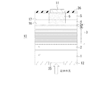
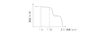
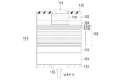
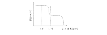
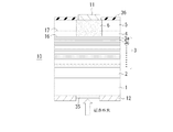
L'invention concerne un élément photorécepteur ou similaire qui offre une sensibilité suffisamment élevée dans la région de longueur d'onde de l'infrarouge proche de 1,5 à 1,8 µm et qui est en mesure de réduire le courant d'obscurité. Un élément photorécepteur (10) selon l'invention comprend une couche tampon (2) disposée adjacente sur le dessus d'un substrat d'InP (1) et une couche photoréceptrice (3) disposée adjacente sur le dessus de la couche tampon. La couche photoréceptrice est formée d'au moins 50 paires, une paire étant une première couche semi-conductrice (3a) ayant une bande interdite de 0,73 eV ou moins et une seconde couche semi-conductrice (3b) ayant une bande interdite supérieure à celle de la première couche semi-conductrice. La première couche semi-conductrice (3a) et la seconde couche semi-conductrice (3b) forment une structure de puits quantique à compensation des contraintes et l'épaisseur de chaque couche est comprise entre 1 nm et 10 nm.
Priority Applications (2)
| Application Number | Priority Date | Filing Date | Title |
|---|---|---|---|
| CN2012800100225A CN103403884A (zh) | 2011-02-23 | 2012-02-03 | 光接收元件及其制造方法 |
| US14/000,187 US20130313521A1 (en) | 2011-02-23 | 2012-02-03 | Photodiode and method for producing the same |
Applications Claiming Priority (2)
| Application Number | Priority Date | Filing Date | Title |
|---|---|---|---|
| JP2011-037182 | 2011-02-23 | ||
| JP2011037182A JP2012174977A (ja) | 2011-02-23 | 2011-02-23 | 受光素子およびその製造方法 |
Publications (1)
| Publication Number | Publication Date |
|---|---|
| WO2012114849A1 true WO2012114849A1 (fr) | 2012-08-30 |
Family
ID=46720637
Family Applications (1)
| Application Number | Title | Priority Date | Filing Date |
|---|---|---|---|
| PCT/JP2012/052478 WO2012114849A1 (fr) | 2011-02-23 | 2012-02-03 | Élément photorécepteur et son procédé de fabrication |
Country Status (5)
| Country | Link |
|---|---|
| US (1) | US20130313521A1 (fr) |
| JP (1) | JP2012174977A (fr) |
| CN (1) | CN103403884A (fr) |
| TW (1) | TW201251090A (fr) |
| WO (1) | WO2012114849A1 (fr) |
Cited By (3)
| Publication number | Priority date | Publication date | Assignee | Title |
|---|---|---|---|---|
| JP2014216624A (ja) * | 2013-04-30 | 2014-11-17 | 住友電気工業株式会社 | エピタキシャルウエハ、その製造方法、半導体素子、および光学センサ装置 |
| US20150162471A1 (en) * | 2012-06-28 | 2015-06-11 | Elta Systems Ltd. | Phototransistor device |
| WO2019044686A1 (fr) * | 2017-09-01 | 2019-03-07 | 住友電気工業株式会社 | Stratifié semi-conducteur, élément de réception de lumière et procédé de fabrication de stratifié semi-conducteur |
Families Citing this family (8)
| Publication number | Priority date | Publication date | Assignee | Title |
|---|---|---|---|---|
| CN102881760B (zh) * | 2012-10-08 | 2016-12-28 | 上海集成电路研发中心有限公司 | 红外感测器及其制造方法 |
| JP6115890B2 (ja) * | 2013-09-13 | 2017-04-19 | 住友電気工業株式会社 | 受光素子、その製造方法、および光センサ装置 |
| JP2015149335A (ja) * | 2014-02-05 | 2015-08-20 | 住友電気工業株式会社 | 半導体積層体、半導体積層体の製造方法および半導体装置の製造方法 |
| JP2015225886A (ja) * | 2014-05-26 | 2015-12-14 | 日本放送協会 | 光電変換素子、光電変換素子の製造方法、積層型固体撮像素子および太陽電池 |
| US10158035B2 (en) * | 2015-04-22 | 2018-12-18 | Sumitomo Electric Industries, Ltd. | Semiconductor stack, light-receiving device, and method for producing semiconductor stack |
| JP6488855B2 (ja) * | 2015-04-22 | 2019-03-27 | 住友電気工業株式会社 | 半導体積層体、受光素子および半導体積層体の製造方法 |
| JP6589662B2 (ja) * | 2016-01-27 | 2019-10-16 | 住友電気工業株式会社 | 半導体積層体および受光素子 |
| JP6613923B2 (ja) * | 2016-01-27 | 2019-12-04 | 住友電気工業株式会社 | 半導体積層体、受光素子および半導体積層体の製造方法 |
Citations (9)
| Publication number | Priority date | Publication date | Assignee | Title |
|---|---|---|---|---|
| JPH0461174A (ja) * | 1990-06-22 | 1992-02-27 | Nec Corp | アバランシェフォトダイオード |
| JPH06188449A (ja) * | 1992-12-21 | 1994-07-08 | Furukawa Electric Co Ltd:The | Msm型受光素子 |
| JPH0774381A (ja) * | 1993-09-01 | 1995-03-17 | Mitsubishi Electric Corp | 半導体受光素子 |
| JPH09219563A (ja) * | 1996-02-09 | 1997-08-19 | Hitachi Ltd | 半導体光素子とそれを用いた応用システム |
| JP2002064217A (ja) * | 2000-06-06 | 2002-02-28 | Fujitsu Quantum Devices Ltd | 半導体受光装置およびその製造方法 |
| JP2008153311A (ja) * | 2006-12-14 | 2008-07-03 | Sumitomo Electric Ind Ltd | 半導体受光素子、視界支援装置および生体医療装置 |
| JP2008288293A (ja) * | 2007-05-16 | 2008-11-27 | Nippon Telegr & Teleph Corp <Ntt> | 半導体受光素子 |
| WO2010073768A1 (fr) * | 2008-12-26 | 2010-07-01 | 住友電気工業株式会社 | Élément de réception de lumière, réseau d'éléments de réception de lumière, procédé de fabrication d'élément de réception de lumière et procédé de fabrication de réseau d'éléments de réception de lumière |
| WO2011016309A1 (fr) * | 2009-08-01 | 2011-02-10 | 住友電気工業株式会社 | Élément semi-conducteur et procédé pour sa fabrication |
Family Cites Families (4)
| Publication number | Priority date | Publication date | Assignee | Title |
|---|---|---|---|---|
| GB0118150D0 (en) * | 2001-07-25 | 2001-09-19 | Imperial College | Thermophotovoltaic device |
| JP5262293B2 (ja) * | 2008-05-26 | 2013-08-14 | 三菱電機株式会社 | 光半導体装置 |
| JP5422990B2 (ja) * | 2008-12-22 | 2014-02-19 | 住友電気工業株式会社 | 生体成分検出装置 |
| JP4840451B2 (ja) * | 2009-01-22 | 2011-12-21 | 住友電気工業株式会社 | 近赤外イメージセンサ |
-
2011
- 2011-02-23 JP JP2011037182A patent/JP2012174977A/ja active Pending
-
2012
- 2012-02-03 WO PCT/JP2012/052478 patent/WO2012114849A1/fr active Application Filing
- 2012-02-03 CN CN2012800100225A patent/CN103403884A/zh active Pending
- 2012-02-03 US US14/000,187 patent/US20130313521A1/en not_active Abandoned
- 2012-02-14 TW TW101104799A patent/TW201251090A/zh unknown
Patent Citations (9)
| Publication number | Priority date | Publication date | Assignee | Title |
|---|---|---|---|---|
| JPH0461174A (ja) * | 1990-06-22 | 1992-02-27 | Nec Corp | アバランシェフォトダイオード |
| JPH06188449A (ja) * | 1992-12-21 | 1994-07-08 | Furukawa Electric Co Ltd:The | Msm型受光素子 |
| JPH0774381A (ja) * | 1993-09-01 | 1995-03-17 | Mitsubishi Electric Corp | 半導体受光素子 |
| JPH09219563A (ja) * | 1996-02-09 | 1997-08-19 | Hitachi Ltd | 半導体光素子とそれを用いた応用システム |
| JP2002064217A (ja) * | 2000-06-06 | 2002-02-28 | Fujitsu Quantum Devices Ltd | 半導体受光装置およびその製造方法 |
| JP2008153311A (ja) * | 2006-12-14 | 2008-07-03 | Sumitomo Electric Ind Ltd | 半導体受光素子、視界支援装置および生体医療装置 |
| JP2008288293A (ja) * | 2007-05-16 | 2008-11-27 | Nippon Telegr & Teleph Corp <Ntt> | 半導体受光素子 |
| WO2010073768A1 (fr) * | 2008-12-26 | 2010-07-01 | 住友電気工業株式会社 | Élément de réception de lumière, réseau d'éléments de réception de lumière, procédé de fabrication d'élément de réception de lumière et procédé de fabrication de réseau d'éléments de réception de lumière |
| WO2011016309A1 (fr) * | 2009-08-01 | 2011-02-10 | 住友電気工業株式会社 | Élément semi-conducteur et procédé pour sa fabrication |
Cited By (7)
| Publication number | Priority date | Publication date | Assignee | Title |
|---|---|---|---|---|
| US20150162471A1 (en) * | 2012-06-28 | 2015-06-11 | Elta Systems Ltd. | Phototransistor device |
| JP2014216624A (ja) * | 2013-04-30 | 2014-11-17 | 住友電気工業株式会社 | エピタキシャルウエハ、その製造方法、半導体素子、および光学センサ装置 |
| US9698287B2 (en) | 2013-04-30 | 2017-07-04 | Sumitomo Electric Industries, Ltd. | Epitaxial wafer, method for producing the same, semiconductor element, and optical sensor device |
| WO2019044686A1 (fr) * | 2017-09-01 | 2019-03-07 | 住友電気工業株式会社 | Stratifié semi-conducteur, élément de réception de lumière et procédé de fabrication de stratifié semi-conducteur |
| JPWO2019044686A1 (ja) * | 2017-09-01 | 2020-08-27 | 住友電気工業株式会社 | 半導体積層体、受光素子および半導体積層体の製造方法 |
| US11081605B2 (en) | 2017-09-01 | 2021-08-03 | Sumitomo Electric Industries, Ltd. | Semiconductor laminate, light-receiving element, and method for manufacturing semiconductor laminate |
| JP7078049B2 (ja) | 2017-09-01 | 2022-05-31 | 住友電気工業株式会社 | 半導体積層体、受光素子および半導体積層体の製造方法 |
Also Published As
| Publication number | Publication date |
|---|---|
| US20130313521A1 (en) | 2013-11-28 |
| TW201251090A (en) | 2012-12-16 |
| JP2012174977A (ja) | 2012-09-10 |
| CN103403884A (zh) | 2013-11-20 |
Similar Documents
| Publication | Publication Date | Title |
|---|---|---|
| WO2012114849A1 (fr) | Élément photorécepteur et son procédé de fabrication | |
| JP5649157B2 (ja) | 半導体素子およびその製造方法 | |
| US9818895B2 (en) | Semiconductor device, optical sensor device and semiconductor device manufacturing method | |
| US9129808B2 (en) | Epitaxial wafer, photodiode, optical sensor device, and methods for producing epitaxial wafer and photodiode | |
| JP5736922B2 (ja) | 受光素子およびその製造方法 | |
| US9190544B2 (en) | Photodiode, optical sensor device, and photodiode manufacturing method | |
| US8822977B2 (en) | Photodetector and method of manufacturing the photodetector | |
| JP6036906B2 (ja) | 受光素子およびその製造方法 | |
| JP5593846B2 (ja) | 受光素子、光学センサ装置および受光素子の製造方法 | |
| JP5776715B2 (ja) | 半導体素子、光学センサ装置および半導体素子の製造方法 | |
| JP2015015476A (ja) | エピタキシャルウェハおよびその製造方法 |
Legal Events
| Date | Code | Title | Description |
|---|---|---|---|
| 121 | Ep: the epo has been informed by wipo that ep was designated in this application |
Ref document number: 12749020 Country of ref document: EP Kind code of ref document: A1 |
|
| WWE | Wipo information: entry into national phase |
Ref document number: 14000187 Country of ref document: US |
|
| NENP | Non-entry into the national phase |
Ref country code: DE |
|
| 122 | Ep: pct application non-entry in european phase |
Ref document number: 12749020 Country of ref document: EP Kind code of ref document: A1 |