WO2012114849A1 - Light-receiving element and method for producing same - Google Patents
Light-receiving element and method for producing same Download PDFInfo
- Publication number
- WO2012114849A1 WO2012114849A1 PCT/JP2012/052478 JP2012052478W WO2012114849A1 WO 2012114849 A1 WO2012114849 A1 WO 2012114849A1 JP 2012052478 W JP2012052478 W JP 2012052478W WO 2012114849 A1 WO2012114849 A1 WO 2012114849A1
- Authority
- WO
- WIPO (PCT)
- Prior art keywords
- layer
- light receiving
- receiving element
- semiconductor layer
- semiconductor
- Prior art date
Links
- 238000004519 manufacturing process Methods 0.000 title claims description 20
- 239000004065 semiconductor Substances 0.000 claims abstract description 118
- 230000035945 sensitivity Effects 0.000 claims abstract description 75
- 239000000758 substrate Substances 0.000 claims abstract description 72
- 239000010410 layer Substances 0.000 claims description 294
- 238000009792 diffusion process Methods 0.000 claims description 37
- 238000009826 distribution Methods 0.000 claims description 29
- 238000000034 method Methods 0.000 claims description 29
- 229910001218 Gallium arsenide Inorganic materials 0.000 claims description 26
- 239000012535 impurity Substances 0.000 claims description 22
- 150000001875 compounds Chemical class 0.000 claims description 17
- 229910052751 metal Inorganic materials 0.000 claims description 16
- 239000002184 metal Substances 0.000 claims description 16
- 238000001947 vapour-phase growth Methods 0.000 claims description 8
- 239000002344 surface layer Substances 0.000 claims description 2
- GPXJNWSHGFTCBW-UHFFFAOYSA-N Indium phosphide Chemical compound [In]#P GPXJNWSHGFTCBW-UHFFFAOYSA-N 0.000 description 92
- 239000007789 gas Substances 0.000 description 46
- 239000010408 film Substances 0.000 description 31
- 230000007704 transition Effects 0.000 description 22
- 125000002524 organometallic group Chemical group 0.000 description 19
- 239000010453 quartz Substances 0.000 description 17
- 239000002994 raw material Substances 0.000 description 17
- VYPSYNLAJGMNEJ-UHFFFAOYSA-N silicon dioxide Inorganic materials O=[Si]=O VYPSYNLAJGMNEJ-UHFFFAOYSA-N 0.000 description 17
- 230000000052 comparative effect Effects 0.000 description 14
- 230000015572 biosynthetic process Effects 0.000 description 11
- 229910000530 Gallium indium arsenide Inorganic materials 0.000 description 10
- 239000013078 crystal Substances 0.000 description 10
- 238000012360 testing method Methods 0.000 description 9
- 238000000354 decomposition reaction Methods 0.000 description 8
- 239000000126 substance Substances 0.000 description 8
- 238000010521 absorption reaction Methods 0.000 description 7
- 230000007423 decrease Effects 0.000 description 7
- 230000007547 defect Effects 0.000 description 7
- 230000001965 increasing effect Effects 0.000 description 7
- IBEFSUTVZWZJEL-UHFFFAOYSA-N trimethylindium Chemical compound C[In](C)C IBEFSUTVZWZJEL-UHFFFAOYSA-N 0.000 description 7
- 238000000927 vapour-phase epitaxy Methods 0.000 description 7
- 229910052799 carbon Inorganic materials 0.000 description 6
- 238000006243 chemical reaction Methods 0.000 description 6
- 239000000463 material Substances 0.000 description 6
- 229910052760 oxygen Inorganic materials 0.000 description 6
- QTQRGDBFHFYIBH-UHFFFAOYSA-N tert-butylarsenic Chemical compound CC(C)(C)[As] QTQRGDBFHFYIBH-UHFFFAOYSA-N 0.000 description 6
- 239000011701 zinc Substances 0.000 description 6
- 238000004891 communication Methods 0.000 description 5
- 238000010586 diagram Methods 0.000 description 5
- 238000002488 metal-organic chemical vapour deposition Methods 0.000 description 5
- RGGPNXQUMRMPRA-UHFFFAOYSA-N triethylgallium Chemical compound CC[Ga](CC)CC RGGPNXQUMRMPRA-UHFFFAOYSA-N 0.000 description 5
- OKTJSMMVPCPJKN-UHFFFAOYSA-N Carbon Chemical compound [C] OKTJSMMVPCPJKN-UHFFFAOYSA-N 0.000 description 4
- QVGXLLKOCUKJST-UHFFFAOYSA-N atomic oxygen Chemical compound [O] QVGXLLKOCUKJST-UHFFFAOYSA-N 0.000 description 4
- 239000001301 oxygen Substances 0.000 description 4
- ZGNPLWZYVAFUNZ-UHFFFAOYSA-N tert-butylphosphane Chemical compound CC(C)(C)P ZGNPLWZYVAFUNZ-UHFFFAOYSA-N 0.000 description 4
- 230000002950 deficient Effects 0.000 description 3
- 238000011156 evaluation Methods 0.000 description 3
- 238000003384 imaging method Methods 0.000 description 3
- 230000001771 impaired effect Effects 0.000 description 3
- IUVCFHHAEHNCFT-INIZCTEOSA-N 2-[(1s)-1-[4-amino-3-(3-fluoro-4-propan-2-yloxyphenyl)pyrazolo[3,4-d]pyrimidin-1-yl]ethyl]-6-fluoro-3-(3-fluorophenyl)chromen-4-one Chemical compound C1=C(F)C(OC(C)C)=CC=C1C(C1=C(N)N=CN=C11)=NN1[C@@H](C)C1=C(C=2C=C(F)C=CC=2)C(=O)C2=CC(F)=CC=C2O1 IUVCFHHAEHNCFT-INIZCTEOSA-N 0.000 description 2
- 229910000661 Mercury cadmium telluride Inorganic materials 0.000 description 2
- XYFCBTPGUUZFHI-UHFFFAOYSA-N Phosphine Chemical compound P XYFCBTPGUUZFHI-UHFFFAOYSA-N 0.000 description 2
- 239000012159 carrier gas Substances 0.000 description 2
- 238000011109 contamination Methods 0.000 description 2
- 238000001816 cooling Methods 0.000 description 2
- 238000000151 deposition Methods 0.000 description 2
- 230000008021 deposition Effects 0.000 description 2
- 238000010438 heat treatment Methods 0.000 description 2
- 230000003287 optical effect Effects 0.000 description 2
- 230000002441 reversible effect Effects 0.000 description 2
- 229910052814 silicon oxide Inorganic materials 0.000 description 2
- 238000009751 slip forming Methods 0.000 description 2
- VCZQFJFZMMALHB-UHFFFAOYSA-N tetraethylsilane Chemical compound CC[Si](CC)(CC)CC VCZQFJFZMMALHB-UHFFFAOYSA-N 0.000 description 2
- 239000010409 thin film Substances 0.000 description 2
- OTRPZROOJRIMKW-UHFFFAOYSA-N triethylindigane Chemical compound CC[In](CC)CC OTRPZROOJRIMKW-UHFFFAOYSA-N 0.000 description 2
- HTDIUWINAKAPER-UHFFFAOYSA-N trimethylarsine Chemical compound C[As](C)C HTDIUWINAKAPER-UHFFFAOYSA-N 0.000 description 2
- XCZXGTMEAKBVPV-UHFFFAOYSA-N trimethylgallium Chemical compound C[Ga](C)C XCZXGTMEAKBVPV-UHFFFAOYSA-N 0.000 description 2
- PORFVJURJXKREL-UHFFFAOYSA-N trimethylstibine Chemical compound C[Sb](C)C PORFVJURJXKREL-UHFFFAOYSA-N 0.000 description 2
- IJGRMHOSHXDMSA-UHFFFAOYSA-N Atomic nitrogen Chemical compound N#N IJGRMHOSHXDMSA-UHFFFAOYSA-N 0.000 description 1
- GYHNNYVSQQEPJS-UHFFFAOYSA-N Gallium Chemical compound [Ga] GYHNNYVSQQEPJS-UHFFFAOYSA-N 0.000 description 1
- OAICVXFJPJFONN-UHFFFAOYSA-N Phosphorus Chemical compound [P] OAICVXFJPJFONN-UHFFFAOYSA-N 0.000 description 1
- VYRDHRYMAZWQJH-UHFFFAOYSA-N [P].P Chemical compound [P].P VYRDHRYMAZWQJH-UHFFFAOYSA-N 0.000 description 1
- 238000009825 accumulation Methods 0.000 description 1
- 238000004458 analytical method Methods 0.000 description 1
- 229910052787 antimony Inorganic materials 0.000 description 1
- WATWJIUSRGPENY-UHFFFAOYSA-N antimony atom Chemical compound [Sb] WATWJIUSRGPENY-UHFFFAOYSA-N 0.000 description 1
- 229910052785 arsenic Inorganic materials 0.000 description 1
- RQNWIZPPADIBDY-UHFFFAOYSA-N arsenic atom Chemical compound [As] RQNWIZPPADIBDY-UHFFFAOYSA-N 0.000 description 1
- 230000015556 catabolic process Effects 0.000 description 1
- 230000008859 change Effects 0.000 description 1
- 238000006731 degradation reaction Methods 0.000 description 1
- 230000000593 degrading effect Effects 0.000 description 1
- 230000003111 delayed effect Effects 0.000 description 1
- 238000011161 development Methods 0.000 description 1
- 230000018109 developmental process Effects 0.000 description 1
- 230000002708 enhancing effect Effects 0.000 description 1
- 229910052733 gallium Inorganic materials 0.000 description 1
- 125000005842 heteroatom Chemical group 0.000 description 1
- 239000001257 hydrogen Substances 0.000 description 1
- 229910052739 hydrogen Inorganic materials 0.000 description 1
- 125000004435 hydrogen atom Chemical class [H]* 0.000 description 1
- 230000006872 improvement Effects 0.000 description 1
- 229910052738 indium Inorganic materials 0.000 description 1
- APFVFJFRJDLVQX-UHFFFAOYSA-N indium atom Chemical compound [In] APFVFJFRJDLVQX-UHFFFAOYSA-N 0.000 description 1
- 238000010030 laminating Methods 0.000 description 1
- 238000012986 modification Methods 0.000 description 1
- 230000004048 modification Effects 0.000 description 1
- 238000005191 phase separation Methods 0.000 description 1
- 229910052698 phosphorus Inorganic materials 0.000 description 1
- 239000011574 phosphorus Substances 0.000 description 1
- 229910000073 phosphorus hydride Inorganic materials 0.000 description 1
- 230000001681 protective effect Effects 0.000 description 1
- 238000001953 recrystallisation Methods 0.000 description 1
- 230000009467 reduction Effects 0.000 description 1
- 238000011160 research Methods 0.000 description 1
- 230000004043 responsiveness Effects 0.000 description 1
- 238000001004 secondary ion mass spectrometry Methods 0.000 description 1
- 239000007787 solid Substances 0.000 description 1
- JBQYATWDVHIOAR-UHFFFAOYSA-N tellanylidenegermanium Chemical compound [Te]=[Ge] JBQYATWDVHIOAR-UHFFFAOYSA-N 0.000 description 1
- RBEXEKTWBGMBDZ-UHFFFAOYSA-N tri(propan-2-yl)stibane Chemical compound CC(C)[Sb](C(C)C)C(C)C RBEXEKTWBGMBDZ-UHFFFAOYSA-N 0.000 description 1
- KKOFCVMVBJXDFP-UHFFFAOYSA-N triethylstibane Chemical compound CC[Sb](CC)CC KKOFCVMVBJXDFP-UHFFFAOYSA-N 0.000 description 1
- 238000007740 vapor deposition Methods 0.000 description 1
Images


Classifications
-
- H—ELECTRICITY
- H01—ELECTRIC ELEMENTS
- H01L—SEMICONDUCTOR DEVICES NOT COVERED BY CLASS H10
- H01L31/00—Semiconductor devices sensitive to infrared radiation, light, electromagnetic radiation of shorter wavelength or corpuscular radiation and specially adapted either for the conversion of the energy of such radiation into electrical energy or for the control of electrical energy by such radiation; Processes or apparatus specially adapted for the manufacture or treatment thereof or of parts thereof; Details thereof
- H01L31/0248—Semiconductor devices sensitive to infrared radiation, light, electromagnetic radiation of shorter wavelength or corpuscular radiation and specially adapted either for the conversion of the energy of such radiation into electrical energy or for the control of electrical energy by such radiation; Processes or apparatus specially adapted for the manufacture or treatment thereof or of parts thereof; Details thereof characterised by their semiconductor bodies
- H01L31/0352—Semiconductor devices sensitive to infrared radiation, light, electromagnetic radiation of shorter wavelength or corpuscular radiation and specially adapted either for the conversion of the energy of such radiation into electrical energy or for the control of electrical energy by such radiation; Processes or apparatus specially adapted for the manufacture or treatment thereof or of parts thereof; Details thereof characterised by their semiconductor bodies characterised by their shape or by the shapes, relative sizes or disposition of the semiconductor regions
- H01L31/035209—Semiconductor devices sensitive to infrared radiation, light, electromagnetic radiation of shorter wavelength or corpuscular radiation and specially adapted either for the conversion of the energy of such radiation into electrical energy or for the control of electrical energy by such radiation; Processes or apparatus specially adapted for the manufacture or treatment thereof or of parts thereof; Details thereof characterised by their semiconductor bodies characterised by their shape or by the shapes, relative sizes or disposition of the semiconductor regions comprising a quantum structures
-
- B—PERFORMING OPERATIONS; TRANSPORTING
- B82—NANOTECHNOLOGY
- B82Y—SPECIFIC USES OR APPLICATIONS OF NANOSTRUCTURES; MEASUREMENT OR ANALYSIS OF NANOSTRUCTURES; MANUFACTURE OR TREATMENT OF NANOSTRUCTURES
- B82Y20/00—Nanooptics, e.g. quantum optics or photonic crystals
-
- C—CHEMISTRY; METALLURGY
- C30—CRYSTAL GROWTH
- C30B—SINGLE-CRYSTAL GROWTH; UNIDIRECTIONAL SOLIDIFICATION OF EUTECTIC MATERIAL OR UNIDIRECTIONAL DEMIXING OF EUTECTOID MATERIAL; REFINING BY ZONE-MELTING OF MATERIAL; PRODUCTION OF A HOMOGENEOUS POLYCRYSTALLINE MATERIAL WITH DEFINED STRUCTURE; SINGLE CRYSTALS OR HOMOGENEOUS POLYCRYSTALLINE MATERIAL WITH DEFINED STRUCTURE; AFTER-TREATMENT OF SINGLE CRYSTALS OR A HOMOGENEOUS POLYCRYSTALLINE MATERIAL WITH DEFINED STRUCTURE; APPARATUS THEREFOR
- C30B25/00—Single-crystal growth by chemical reaction of reactive gases, e.g. chemical vapour-deposition growth
- C30B25/02—Epitaxial-layer growth
- C30B25/18—Epitaxial-layer growth characterised by the substrate
- C30B25/183—Epitaxial-layer growth characterised by the substrate being provided with a buffer layer, e.g. a lattice matching layer
-
- C—CHEMISTRY; METALLURGY
- C30—CRYSTAL GROWTH
- C30B—SINGLE-CRYSTAL GROWTH; UNIDIRECTIONAL SOLIDIFICATION OF EUTECTIC MATERIAL OR UNIDIRECTIONAL DEMIXING OF EUTECTOID MATERIAL; REFINING BY ZONE-MELTING OF MATERIAL; PRODUCTION OF A HOMOGENEOUS POLYCRYSTALLINE MATERIAL WITH DEFINED STRUCTURE; SINGLE CRYSTALS OR HOMOGENEOUS POLYCRYSTALLINE MATERIAL WITH DEFINED STRUCTURE; AFTER-TREATMENT OF SINGLE CRYSTALS OR A HOMOGENEOUS POLYCRYSTALLINE MATERIAL WITH DEFINED STRUCTURE; APPARATUS THEREFOR
- C30B29/00—Single crystals or homogeneous polycrystalline material with defined structure characterised by the material or by their shape
- C30B29/10—Inorganic compounds or compositions
- C30B29/40—AIIIBV compounds wherein A is B, Al, Ga, In or Tl and B is N, P, As, Sb or Bi
- C30B29/42—Gallium arsenide
-
- C—CHEMISTRY; METALLURGY
- C30—CRYSTAL GROWTH
- C30B—SINGLE-CRYSTAL GROWTH; UNIDIRECTIONAL SOLIDIFICATION OF EUTECTIC MATERIAL OR UNIDIRECTIONAL DEMIXING OF EUTECTOID MATERIAL; REFINING BY ZONE-MELTING OF MATERIAL; PRODUCTION OF A HOMOGENEOUS POLYCRYSTALLINE MATERIAL WITH DEFINED STRUCTURE; SINGLE CRYSTALS OR HOMOGENEOUS POLYCRYSTALLINE MATERIAL WITH DEFINED STRUCTURE; AFTER-TREATMENT OF SINGLE CRYSTALS OR A HOMOGENEOUS POLYCRYSTALLINE MATERIAL WITH DEFINED STRUCTURE; APPARATUS THEREFOR
- C30B29/00—Single crystals or homogeneous polycrystalline material with defined structure characterised by the material or by their shape
- C30B29/60—Single crystals or homogeneous polycrystalline material with defined structure characterised by the material or by their shape characterised by shape
- C30B29/68—Crystals with laminate structure, e.g. "superlattices"
-
- H—ELECTRICITY
- H01—ELECTRIC ELEMENTS
- H01L—SEMICONDUCTOR DEVICES NOT COVERED BY CLASS H10
- H01L31/00—Semiconductor devices sensitive to infrared radiation, light, electromagnetic radiation of shorter wavelength or corpuscular radiation and specially adapted either for the conversion of the energy of such radiation into electrical energy or for the control of electrical energy by such radiation; Processes or apparatus specially adapted for the manufacture or treatment thereof or of parts thereof; Details thereof
- H01L31/0248—Semiconductor devices sensitive to infrared radiation, light, electromagnetic radiation of shorter wavelength or corpuscular radiation and specially adapted either for the conversion of the energy of such radiation into electrical energy or for the control of electrical energy by such radiation; Processes or apparatus specially adapted for the manufacture or treatment thereof or of parts thereof; Details thereof characterised by their semiconductor bodies
- H01L31/0352—Semiconductor devices sensitive to infrared radiation, light, electromagnetic radiation of shorter wavelength or corpuscular radiation and specially adapted either for the conversion of the energy of such radiation into electrical energy or for the control of electrical energy by such radiation; Processes or apparatus specially adapted for the manufacture or treatment thereof or of parts thereof; Details thereof characterised by their semiconductor bodies characterised by their shape or by the shapes, relative sizes or disposition of the semiconductor regions
- H01L31/035236—Superlattices; Multiple quantum well structures
-
- H—ELECTRICITY
- H01—ELECTRIC ELEMENTS
- H01L—SEMICONDUCTOR DEVICES NOT COVERED BY CLASS H10
- H01L31/00—Semiconductor devices sensitive to infrared radiation, light, electromagnetic radiation of shorter wavelength or corpuscular radiation and specially adapted either for the conversion of the energy of such radiation into electrical energy or for the control of electrical energy by such radiation; Processes or apparatus specially adapted for the manufacture or treatment thereof or of parts thereof; Details thereof
- H01L31/08—Semiconductor devices sensitive to infrared radiation, light, electromagnetic radiation of shorter wavelength or corpuscular radiation and specially adapted either for the conversion of the energy of such radiation into electrical energy or for the control of electrical energy by such radiation; Processes or apparatus specially adapted for the manufacture or treatment thereof or of parts thereof; Details thereof in which radiation controls flow of current through the device, e.g. photoresistors
- H01L31/10—Semiconductor devices sensitive to infrared radiation, light, electromagnetic radiation of shorter wavelength or corpuscular radiation and specially adapted either for the conversion of the energy of such radiation into electrical energy or for the control of electrical energy by such radiation; Processes or apparatus specially adapted for the manufacture or treatment thereof or of parts thereof; Details thereof in which radiation controls flow of current through the device, e.g. photoresistors characterised by at least one potential-jump barrier or surface barrier, e.g. phototransistors
- H01L31/101—Devices sensitive to infrared, visible or ultraviolet radiation
- H01L31/102—Devices sensitive to infrared, visible or ultraviolet radiation characterised by only one potential barrier or surface barrier
- H01L31/109—Devices sensitive to infrared, visible or ultraviolet radiation characterised by only one potential barrier or surface barrier the potential barrier being of the PN heterojunction type
-
- H—ELECTRICITY
- H01—ELECTRIC ELEMENTS
- H01L—SEMICONDUCTOR DEVICES NOT COVERED BY CLASS H10
- H01L31/00—Semiconductor devices sensitive to infrared radiation, light, electromagnetic radiation of shorter wavelength or corpuscular radiation and specially adapted either for the conversion of the energy of such radiation into electrical energy or for the control of electrical energy by such radiation; Processes or apparatus specially adapted for the manufacture or treatment thereof or of parts thereof; Details thereof
- H01L31/18—Processes or apparatus specially adapted for the manufacture or treatment of these devices or of parts thereof
- H01L31/184—Processes or apparatus specially adapted for the manufacture or treatment of these devices or of parts thereof the active layers comprising only AIIIBV compounds, e.g. GaAs, InP
- H01L31/1844—Processes or apparatus specially adapted for the manufacture or treatment of these devices or of parts thereof the active layers comprising only AIIIBV compounds, e.g. GaAs, InP comprising ternary or quaternary compounds, e.g. Ga Al As, In Ga As P
-
- Y—GENERAL TAGGING OF NEW TECHNOLOGICAL DEVELOPMENTS; GENERAL TAGGING OF CROSS-SECTIONAL TECHNOLOGIES SPANNING OVER SEVERAL SECTIONS OF THE IPC; TECHNICAL SUBJECTS COVERED BY FORMER USPC CROSS-REFERENCE ART COLLECTIONS [XRACs] AND DIGESTS
- Y02—TECHNOLOGIES OR APPLICATIONS FOR MITIGATION OR ADAPTATION AGAINST CLIMATE CHANGE
- Y02E—REDUCTION OF GREENHOUSE GAS [GHG] EMISSIONS, RELATED TO ENERGY GENERATION, TRANSMISSION OR DISTRIBUTION
- Y02E10/00—Energy generation through renewable energy sources
- Y02E10/50—Photovoltaic [PV] energy
- Y02E10/544—Solar cells from Group III-V materials
-
- Y—GENERAL TAGGING OF NEW TECHNOLOGICAL DEVELOPMENTS; GENERAL TAGGING OF CROSS-SECTIONAL TECHNOLOGIES SPANNING OVER SEVERAL SECTIONS OF THE IPC; TECHNICAL SUBJECTS COVERED BY FORMER USPC CROSS-REFERENCE ART COLLECTIONS [XRACs] AND DIGESTS
- Y02—TECHNOLOGIES OR APPLICATIONS FOR MITIGATION OR ADAPTATION AGAINST CLIMATE CHANGE
- Y02P—CLIMATE CHANGE MITIGATION TECHNOLOGIES IN THE PRODUCTION OR PROCESSING OF GOODS
- Y02P70/00—Climate change mitigation technologies in the production process for final industrial or consumer products
- Y02P70/50—Manufacturing or production processes characterised by the final manufactured product
Definitions
- the present invention relates to a light receiving element and a method for manufacturing the same. More specifically, a light-receiving element including a light-receiving layer having a multiple quantum well structure (Multiple-Quantum ⁇ Well, hereinafter referred to as MQW) that secures sensitivity in the near-infrared wavelength region of 1.5 ⁇ m to 1.8 ⁇ m and its It relates to a manufacturing method.
- MQW multiple quantum well structure
- Non-Patent Document 1 proposes a photodiode having a cut-off wavelength of 2.39 ⁇ m by forming an InGaAs / GaAsSb type 2 MQW on an InP substrate and a pn junction formed by a p-type or n-type epitaxial layer. Sensitivity characteristics with wavelengths of 1.7 ⁇ m to 2.7 ⁇ m are shown.
- Non-Patent Document 2 shows the sensitivity characteristic (200K, 250K, 295K) of a wavelength of 1 ⁇ m to 3 ⁇ m of a light receiving element having a type 2 MQW light receiving layer in which 150 pairs of InGaAs 5 nm and GaAsSb 5 nm are stacked as a pair.
- Patent Document 1 gives an InP substrate and a lattice constant smaller than the lattice constant of the InP substrate formed on the InP substrate in order to slightly expand the upper limit wavelength of the light receiving region for optical communication.
- a photodiode including, in a light-receiving layer, In 0.53 Ga 0.47 As (first absorption layer) having a composition and In 0.55 Ga 0.45 As (second absorption layer) having a composition that provides a large lattice constant. Proposed. According to this, the light receiving area can be lengthened to a wavelength of about 1700 nm.
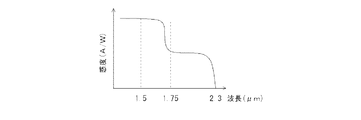
- the important absorption band of the substance is concentrated in the wavelength range of 1.5 ⁇ m to 1.8 ⁇ m, if a clear image with sufficiently high sensitivity can be obtained in this wavelength range of 1.5 ⁇ m to 1.8 ⁇ m, Use can be promoted.
- the sensitivity suddenly decreases from around a slightly long wavelength of 1.6 ⁇ m (see FIG. 6). This is because photoelectric current is generated by photoelectric conversion of both type 2 transition and type 1 transition. Due to this influence, the contribution of the type 1 transition is reduced from around the wavelength of 1.65 ⁇ m.
- the light receiving element of the present invention is a light receiving element made of a III-V group compound semiconductor formed on an InP substrate.
- the light receiving element includes a buffer layer positioned in contact with the InP substrate and a light receiving layer positioned in contact with the buffer layer.
- the light receiving layer is formed by alternately laminating a first semiconductor layer having a band gap energy of 0.73 eV or less and a second semiconductor layer having a band gap energy larger than the band gap energy of the first semiconductor layer. 50 pairs or more are included, the first semiconductor layer and the second semiconductor layer form a strain compensation quantum well structure, and the thicknesses of the first semiconductor layer and the second semiconductor layer are both 1 nm or more and 10 nm or less. It is characterized by.
- the band gap energy of the first semiconductor layer is 0.73 eV or less, high light receiving sensitivity can be obtained at a wavelength of 1.7 ⁇ m to 1.8 ⁇ m based on the type 1 transition in the first semiconductor layer.
- the first semiconductor layer has a larger lattice constant than the InP substrate, while the second semiconductor layer has a smaller lattice constant. Compressive stress and tensile stress are distributed in the latter, and both form a strain compensated quantum well structure.
- the first semiconductor layer / second semiconductor layer is 50 pairs or more, and the thickness of each semiconductor layer is 1 nm or more and 10 nm or less, so that the compressive strain and tensile strain due to lattice mismatch are balanced and the strain is macroscopically. The influence can be reduced. By avoiding the accumulation of this strain, the crystallinity can be improved and an increase in dark current can be prevented. That is, dark current can be kept low while having high light receiving sensitivity in the vicinity of a wavelength of 1.5 ⁇ m to 1.8 ⁇ m.
- MCT HgCdTe
- the first semiconductor layer and the second semiconductor layer can be (1) a type 2 multiple quantum well structure or (2) the same compound semiconductor having a different composition.
- the strain compensation quantum well structure may be (1) a type 2 multiple quantum well structure, or (2) a composition having a different composition, for example, InGaAs may be used.
- the dark current is kept low while having high light receiving sensitivity in the vicinity of the wavelength of 1.5 ⁇ m to 1.8 ⁇ m where the absorption bands important for the substance are concentrated. be able to.
- the total film thickness in the light receiving layer of the first semiconductor layer is preferably 0.5 ⁇ m or more. As a result, it is possible to ensure sensitivity especially at the upper limit near the wavelength of 1.75 ⁇ m. The light reception in the vicinity of the wavelength of 1.75 ⁇ m is due to the type 1 transition in the bulk of the first semiconductor layer. Therefore, the sensitivity can be ensured by setting the total film thickness to 0.5 ⁇ m or more.
- the band gap energy of the buffer layer is preferably larger than the band gap energy of either the first semiconductor layer or the second semiconductor layer. This prevents light from being absorbed by the buffer layer in the case of substrate backside incidence (necessary for two-dimensional array of pixels). Further, the band gap energy of InP (substrate) is 1.27 eV, and naturally, there is no possibility of absorbing light in the wavelength region currently in question.
- the first semiconductor layer can be In x Ga 1-x As (0.56 ⁇ x ⁇ 0.68). This makes it possible to obtain a first semiconductor layer that can reliably receive light with a wavelength of 1.7 ⁇ m to 1.8 ⁇ m in the type 1 transition.
- the second semiconductor layer can be In y Ga 1-y As (0.38 ⁇ y ⁇ 0.50).
- the strain compensation quantum well structure can be easily formed by combining the second semiconductor layer with a lattice constant smaller than InP and the first semiconductor layer having a lattice constant larger than InP.
- the crystallinity of the entire epitaxial layer including the window layer can be improved, and the dark current can be reduced.
- this second semiconductor layer can also receive light by the type 1 transition, but the upper limit of the wavelength that can be received is in a range shorter than 1.7 ⁇ m.
- the second semiconductor layer can be GaAs z Sb 1-z (0.54 ⁇ z ⁇ 0.66). Also in this case, the strain compensation quantum well structure can be easily formed by combining the second semiconductor layer with a lattice constant smaller than that of InP and the first semiconductor layer having a lattice constant larger than that of InP. In this case, since Sb that is difficult to handle is reduced, it is preferable for enhancing the crystallinity of the entire epitaxial layer and suppressing dark current. In this case, type 2 transition is possible, and not only the long wavelength side with a wavelength of 1.8 ⁇ m or longer, but also light in the wavelength range of 1.7 ⁇ m to 1.8 ⁇ m, which is the focal point, is received by the type 2 transition. can do. That is, not only light having a wavelength of 1.7 ⁇ m to 1.8 ⁇ m due to the type 1 transition by the first semiconductor layer but also light having a wavelength of 1.7 ⁇ m to 1.8 ⁇ m can be received by the type 2 transition.
- the all-organic metal vapor phase growth method refers to a growth method in which an organic metal raw material composed of a compound of an organic substance and a metal is used for all the raw materials for vapor phase growth, and is referred to as a total organic MOVPE method.
- the buffer layer can include P.
- Examples of cases where P is contained in the buffer layer include an InP buffer layer and an InGaAsP buffer layer. These buffer layers are easy to grow a good crystalline thin film. For this reason, the crystallinity of the light receiving layer (first and second semiconductor layers) grown in contact with the buffer layer can be improved, and as a result, the dark current can be lowered.
- a substrate back surface incident structure for making the back surface of the InP substrate the incident surface can be provided.
- the structure in which light is incident from the back side of the substrate means (1) bonding bumps provided on the pixel electrode on the surface side of the epitaxial layer (the readout circuit covers the surface side of the epitaxial layer), (2) An anti-reflection film (AR film) provided on the back side of the substrate, (3) a two-dimensional arrangement of light receiving elements (pixels) as a basic unit, which must be incident on the back side of the substrate (others) An example structure will be described later).
- the substrate backside incident structure described above it is possible to manufacture a light receiving element having two-dimensionally arrayed pixels while maintaining a low dark current and ensuring high sensitivity.
- III-V group compound semiconductor diffusion concentration distribution adjustment layer having a pn junction at the front end of the impurity introduced by selective diffusion and in contact with the upper surface of the light receiving layer opposite to the InP substrate, and adjustment of the diffusion concentration distribution thereof And a window layer containing P in contact with the layer, and the band gap energy of the diffusion concentration distribution adjusting layer is preferably made smaller than the band gap energy of the window layer.
- a light receiving element made of a III-V group compound semiconductor formed on an InP substrate is manufactured.
- This manufacturing method includes a step of forming a buffer layer on an InP substrate, a first semiconductor layer having a band gap of 0.73 eV or less on the buffer layer, and a first semiconductor layer having a band gap larger than that of the first semiconductor layer. And forming a light-receiving layer having a multiple quantum well structure by alternately stacking 50 pairs or more of both the first and second semiconductor layers with a thickness of 1 nm to 10 nm.
- the growth is performed at a growth temperature or a substrate temperature of 600 ° C. or less by a total organometallic vapor phase growth method.
- the light receiving layer has a strain compensated quantum well structure, and it is important whether or not good crystallinity can be obtained.
- the growth temperature or the substrate temperature can be lowered, so that the degree of crystallinity degradation due to thermal expansion caused by the temperature difference can be kept low when cooling after growth.
- the growth temperature or the substrate temperature is a substrate surface temperature monitored by a pyrometer including an infrared camera and an infrared spectrometer. Accordingly, although it is the substrate surface temperature, strictly speaking, it is the temperature of the epitaxial layer surface in a state where a film is formed on the substrate.
- a substrate temperature, a growth temperature, and a film formation temperature There are various names such as a substrate temperature, a growth temperature, and a film formation temperature, and all refer to the monitored temperatures.
- a step of forming a group III-V compound semiconductor layer on the light-receiving layer, and from the start of forming the light-receiving layer until the end of the formation of the group III-V compound semiconductor layer, the same by the all-organic metal vapor phase epitaxy method It is preferable to grow in the deposition chamber.
- all metal organic vapor phase epitaxy all metal organic vapor phase epitaxy
- the dark current can be lowered with a sufficiently high sensitivity stably in the near infrared wavelength range of 1.5 ⁇ m to 1.8 ⁇ m.
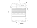
- the light-receiving layer 3 has a multiple quantum well structure formed by stacking 200 pairs of In 0.59 Ga 0.41 As3a and GaAs 0.57 Sb 0.43 3b.
- the film thicknesses of In 0.59 Ga 0.41 As3a and GaAs 0.57 Sb 0.43 3b in the quantum well are both 5 nm.
- the oxygen and carbon concentrations are both less than 1 ⁇ 10 17 cm ⁇ 3 .
- the light receiving layer 103 has a multiple quantum well structure formed by stacking 200 pairs of In 0.53 Ga 0.47 As 103 a and GaAs 0.51 Sb 0.49 103 b.
- the film thicknesses of In 0.53 Ga 0.47 As and GaAs 0.51 Sb 0.49 in the quantum well are both 5 nm. It is a figure which shows the wavelength dependence of the light reception sensitivity of the light receiving element of FIG. It is a figure which shows the light receiving element in Embodiment 2 of this invention.
- the light-receiving layer 3 has a multiple quantum well structure formed by stacking 200 pairs of In 0.59 Ga 0.41 As3a and In 0.47 Ga 0.53 As3c.
- the thicknesses of In 0.59 Ga 0.41 As3a and In 0.47 Ga 0.53 As3c in the quantum well are both 5 nm.
- the oxygen and carbon concentrations are both less than 1 ⁇ 10 17 cm ⁇ 3 . It is a figure which shows the wavelength dependence of the light reception sensitivity of the light receiving element of FIG. It is a flowchart of the manufacturing method of the light receiving element shown in FIG.
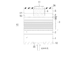
- the p-type region 6 is formed by selectively diffusing Zn of the p-type impurity from the opening of the selective diffusion mask pattern 36 of the SiN film. It is diffused by using the selective diffusion mask pattern 36 of the SiN film that the periphery is limited in a plane and is introduced into the inside of the periphery of the light receiving element 10 and the light receiving part is formed inside the periphery. It is realized by.
- a p-side electrode 11 made of AuZn is provided in the p-type region 6, and an n-side electrode 12 made of AuGeNi is provided in ohmic contact with the back surface of the InP substrate 1.
- the InP substrate 1 is doped with n-type impurities to ensure a predetermined level of conductivity.
- an AR (Anti-reflection) film 35 made of SiON or the like covers the back surface of the InP substrate 1.
- the AR film 35 disposed on the back surface of the InP substrate 1 may be regarded as a structure for entering from the substrate side.
- disposing the pixel electrode (p-side electrode) 11 near or near the center instead of the end of the top surface of the semiconductor stacked body means that light does not enter from the top surface of the semiconductor stacked body, It can be said that the light is incident from the back side of the semiconductor substrate.
- a structure in which bonding bumps for bonding to the reading electrodes of the reading circuit are arranged on the pixel electrodes can also be referred to as a structure for incident on the back surface of the semiconductor substrate. This is because the readout circuit covers the entire pixel side.
- the structure in which both the ground electrode and the pixel electrode extend to the surface side of the epitaxial layer is definitely a structure for incident on the back surface of the substrate.
- the structure for the back surface incidence of the semiconductor substrate necessarily exists in the light receiving element that is not limited to these exemplified structures and is incident on the back surface of the substrate. Further, since the two-dimensional array of pixels P itself is a flip-flop junction system used for connection with the readout circuit, the substrate back surface incidence is inevitable, and the above structure is for entering from the substrate back surface.
- a pn junction is formed at a position corresponding to the boundary front of the p-type region 6, and a reverse bias voltage is applied between the p-side electrode 11 and the n-side electrode 12.
- the lower side (n-type impurity background) produces a wider depletion layer.
- the background impurity concentration in the light-receiving layer 3 having the multiple quantum well structure is about 5 ⁇ 10 15 cm ⁇ 3 or less in terms of n-type impurity concentration (carrier concentration).
- the position of the pn junction is determined by the intersection of the background impurity concentration (n-type carrier concentration) of the light-receiving layer 3 of the multiple quantum well and the Zn concentration profile of the p-type impurity.
- the concentration of the p-type impurity selectively diffused from the surface of the InP window layer 5 sharply decreases from the high concentration region on the InP window layer side to the light receiving layer side. Therefore, in the light receiving layer 3, an impurity concentration of 5 ⁇ 10 16 cm ⁇ 3 or less can be easily realized.
- the light receiving element 10 targeted by the present invention seeks to have light receiving sensitivity from the near infrared region to the long wavelength side, a material having a band gap energy larger than the band gap energy of the light receiving layer 3 is used for the window layer. It is preferable to use it. For this reason, InP, which is a material having a band gap energy larger than that of the light receiving layer and having a good lattice matching, is usually used for the window layer. InAlAs having substantially the same band gap energy as InP may be used.
- the lattice constant of the second semiconductor layer 3b can be made smaller than InP. Since the composition lattice-matched to InP is GaAs 0.51 Sb 0.49 , the As composition z is larger and the Sb composition (1-z) is much smaller than this. As a result, in combination with the first semiconductor layer 3a, compressive stress is distributed in the first semiconductor layer 3a and tensile stress is distributed in the second semiconductor layer 3b, so that a strain compensation quantum well structure is obtained. it can. As a result, a low distortion state, that is, a low lattice defect density state can be realized, and the dark current can be reduced.
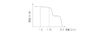
- FIG. 2 is a diagram showing the wavelength dependence of the sensitivity of the light receiving element 10 shown in FIG. From the above (1) to (3), it can be seen that the sensitivity at a wavelength of 1.5 ⁇ m to 1.75 ⁇ m is at a high level in a substantially flat state continuously from the sensitivity on the shorter wavelength side.
- the upper limit of the receivable wavelength is about 2.3 ⁇ m.
- FIG. 3 shows a piping system and the like of the film formation apparatus 60 of the all-organic metal vapor phase epitaxy method.
- a quartz tube 65 is disposed in the reaction chamber (chamber) 63, and a raw material gas is introduced into the quartz tube 65.
- a substrate table 66 is disposed in the quartz tube 65 so as to be rotatable and airtight.
- the substrate table 66 is provided with a heater 66h for heating the substrate.
- the temperature of the surface of the wafer 50 a during film formation is monitored by the infrared temperature monitor device 61 through a window 69 provided in the ceiling of the reaction chamber 63. This monitored temperature is a temperature at the time of growth or a temperature called a film forming temperature or a substrate temperature.
- 600 ° C. or lower is a temperature measured by this temperature monitor.
- the forced exhaust from the quartz tube 65 is performed by a vacuum pump.
- the source gas is supplied by a pipe communicating with the quartz tube 65.
- the all-organometallic vapor phase growth method is characterized in that all source gases are supplied in the form of an organometallic gas.
- source gases such as impurities are not specified, but impurities are also introduced in the form of an organometallic gas.
- the raw material of the organometallic gas is put in a thermostat and kept at a constant temperature. Hydrogen (H 2 ) and nitrogen (N 2 ) are used as the carrier gas.
- the organometallic gas is transported by a transport gas, and is sucked by a vacuum pump and introduced into the quartz tube 65.
- the amount of carrier gas is accurately adjusted by an MFC (Mass Flow Controller). Many flow controllers, electromagnetic valves, and the like are automatically controlled by a microcomputer.
- MFC Mass Flow Controller
- the crystallinity of the InP substrate located in the lower layer is not deteriorated by heating at about 600 ° C.
- the substrate temperature is strictly maintained, for example, in the range of 400 ° C. or more and 600 ° C. or less. There is a need to. The reason is that when heated above 600 ° C., GaAs 0.57 Sb 0.43 is damaged by heat and crystallinity is greatly deteriorated, and when an InP window layer is formed at a temperature lower than 400 ° C.
- the buffer layer 2 may be an InP layer alone, but in a predetermined case, an n-type doped In 0.53 Ga 0.47 As layer is formed on the InP buffer layer with a thickness of 0.15 ⁇ m (150 nm). You may grow into. This In 0.53 Ga 0.47 As layer is also included in the buffer layer 2 in FIG.
- a type 2 MQW light-receiving layer 3 having In 0.59 Ga 0.41 As3a / GaAs 0.57 Sb 0.43 3b as a pair of quantum wells is formed.
- the film thicknesses of In 0.59 Ga 0.41 As3a and GaAs 0.57 Sb 0.43 3b in the quantum well are 1 nm or more and 10 nm or less.
- the MQW light-receiving layer 3 is formed by stacking 200 pairs of quantum wells.
- triethylgallium (TEGa), tertiary butylarsine (TBAs) and trimethylantimony (TMSb) are used.
- TEGa, TMIn, and TBAs can be used.
- These source gases are all organometallic gases, and the molecular weight of the compound is large. Therefore, it can be completely decomposed at a relatively low temperature of 400 ° C. or higher and 600 ° C. or lower and contribute to crystal growth.
- the temperature difference from the film formation temperature to room temperature can be reduced, the strain caused by the difference in thermal expansion of each material in the light receiving element 10 can be reduced, and the lattice defect density can be reduced. This is effective in suppressing dark current.
- the raw material for Ga (gallium) may be TEGa (triethylgallium) or TMGa (trimethylgallium).
- the raw material for In (indium) may be TMIn (trimethylindium) or TEIn (triethylindium).
- As (arsenic) TBAs (tertiary butylarsine) or TMAs (trimethylarsenic) may be used.
- Sb (antimony) may be TMSb (trimethylantimony), TESb (triethylantimony), TIPSb (triisopropylantimony), or TDMASb (tridimethylaminoantimony).
- a semiconductor element having a low MQW impurity concentration and excellent crystallinity can be obtained.
- a light receiving element with a small dark current and a high sensitivity can be obtained. Furthermore, it is possible to capture a clear image even with weak light using the light receiving element.
- the source gas is transported through the piping, introduced into the quartz tube 65, and exhausted. Any number of source gases can be supplied to the quartz tube 65 by increasing the number of pipes. For example, even a dozen kinds of source gases are controlled by opening and closing the electromagnetic valve.
- the flow rate of the source gas is controlled by a flow rate controller (MFC) shown in FIG. 3, and the flow into the quartz tube 65 is turned on and off by opening and closing the electromagnetic valve.
- MFC flow rate controller
- the quartz tube 65 is forcibly exhausted by a vacuum pump. There is no stagnation in the flow of the source gas, and it is performed smoothly and automatically. Therefore, the composition is switched quickly when forming the quantum well pair.
- the temperature distribution of the source gas does not have the directivity as on the inflow side or the outlet side of the source gas.
- the wafer 50a revolves on the substrate table 66, the flow of the source gas near the surface of the wafer 50a is in a turbulent state, and even the source gas near the surface of the wafer 50a contacts the wafer 50a. Except for the raw material gas, it has a large velocity component in the flow direction from the introduction side to the exhaust side. Therefore, most of the heat flowing from the substrate table 66 to the source gas through the wafer 50a is always exhausted together with the exhaust gas.
- the substrate temperature is heated to a low temperature range of 400 ° C. or more and 600 ° C. or less.
- the decomposition efficiency of the raw material is good, so that multiple quantum wells with the raw material gas flowing in a range very close to the wafer 50a
- the source gas that contributes to the growth of the structure is limited to one that is efficiently decomposed into the shape necessary for growth.
- the surface of the wafer 50a is set to a monitored temperature.
- the temperature suddenly decreases or a large temperature step is generated as described above. Therefore, in the case of a raw material gas having a decomposition temperature of T1 ° C., the substrate surface temperature is set to (T1 + ⁇ ), and ⁇ is determined in consideration of variations in temperature distribution and the like.
- T1 + ⁇ the substrate surface temperature
- ⁇ is determined in consideration of variations in temperature distribution and the like.
- the range is limited to the range of the thickness of the organic metal molecules corresponding to several from the surface. Therefore, organometallic molecules in the range in contact with the wafer surface and molecules located within the film thickness range of several organometallic molecules from the wafer surface mainly contribute to the crystal growth, and the outer organic molecules. It is considered that the metal molecules are discharged out of the quartz tube 65 with almost no decomposition. When the organometallic molecules near the surface of the wafer 50a are decomposed and crystal growth occurs, the organometallic molecules located outside enter the replenishment.
- the range of the organometallic molecules that can participate in crystal growth is limited to a thin source gas layer on the surface of the wafer 50a by making the wafer surface temperature slightly higher than the temperature at which the organometallic molecules decompose. it can.
- phase separation occurs in the GaAsSb layer of the multiple quantum well structure when grown in a temperature range exceeding 600 ° C., and the crystal growth surface of the multiple quantum well structure that is clean and excellent in flatness, and A multiple quantum well structure having excellent periodicity and crystallinity cannot be obtained.
- the growth temperature is set to a temperature range of 400 ° C. or more and 600 ° C. or less.
- this film-forming method is an all-organic MOVPE method and all the source gases are made into organometallic gases with high decomposition efficiency. is there.
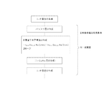
- FIG. 4 is a flowchart of a method for manufacturing a light receiving element.
- an In 0.53 Ga 0.47 As diffusion concentration distribution adjusting layer 4 lattice-matched to InP is located on the type 2 MQW light receiving layer 3, and the In 0.53
- the InP window layer 5 is located on the Ga 0.47 As diffusion concentration distribution adjusting layer 4.
- the p-type region 6 is provided by selectively diffusing Zn of the p-type impurity from the opening of the selective diffusion mask pattern 36 provided on the surface of the InP window layer 5.
- a pn junction or a pi junction is formed at the tip of the p-type region 6.
- a reverse bias voltage is applied to the pn junction or pi junction to form a depletion layer, and the charge due to photoelectron conversion is captured, so that the brightness of the pixel corresponds to the amount of charge.
- the p-type region 6 or the pn junction or pi junction is the main part constituting the pixel.
- the p-side electrode 11 that is in ohmic contact with the p-type region 6 is a pixel electrode, and reads the above charges for each pixel with the n-side electrode 12 that is set to the ground potential.
- the selective diffusion mask pattern 36 is left as it is on the surface of the InP window layer around the p-type region 6. Further, a protective film such as SiON not shown is coated. The selective diffusion mask pattern 36 is left as it is.
- the interfaces 16 and 17 are not regrowth interfaces. Therefore, at the interfaces 16 and 17 of the light receiving element 10 shown in FIG. 1, the oxygen and carbon concentrations are both below 1 ⁇ 10 17 cm ⁇ 3 and below a predetermined level, and in particular, the p-type region 6 and the interface 17 No charge leakage occurs at the intersection line. Also, the lattice defect density can be kept low at the interface 16.
- a non-doped In 0.53 Ga 0.47 As diffusion concentration distribution layer 4 having a film thickness of 1.0 ⁇ m, for example, is formed on the MQW light-receiving layer 3.
- the In 0.53 Ga 0.47 As diffusion concentration distribution layer 4 allows Zn of p-type impurities to reach the MQW light-receiving layer 3 from the InP window layer 5 by a selective diffusion method.
- the In 0.53 Ga 0.47 As diffusion concentration distribution adjusting layer 4 may be arranged as described above, but may not be provided.
- a p-type region 6 is formed by the selective diffusion described above, and a pn junction or a pi junction is formed at the tip thereof. Even when the In 0.53 Ga 0.47 As diffusion concentration distribution adjusting layer 4 is inserted, since the band gap of In 0.53 Ga 0.47 As is small, the electric resistance of the light receiving element is reduced even if it is non-doped. Can be lowered. By reducing the electrical resistance, it is possible to improve the responsiveness and obtain a moving image with good image quality. On the In 0.53 Ga 0.47 As diffusion concentration distribution adjusting layer 4, the undoped InP window layer 5 is continuously formed by the all-organic metal vapor phase epitaxy method while the wafer 50 a is disposed in the same quartz tube 65.
- the growth temperature of the InP window layer 5 can be made 400 ° C. or more and 600 ° C. or less, and further 550 ° C. or less.
- the MQW GaAsSb located under the InP window layer 5 is not damaged by heat, and the MQW crystallinity is not impaired.
- the interface between the In 0.53 Ga 0.47 As diffusion concentration distribution adjusting layer and the InP window layer was a regrowth interface once exposed to the atmosphere.
- the regrowth interface is identified by satisfying at least one of the oxygen concentration of 1 ⁇ 10 17 cm ⁇ 3 or more and the carbon concentration of 1 ⁇ 10 17 cm ⁇ 3 or more by secondary ion mass spectrometry. Can do.
- the regrowth interface forms a crossing line with the p-type region, and a charge leak occurs at the crossing line, thereby significantly degrading the image quality.
- MOVPE method total organic MOCVD not
- the decomposition temperature is high, GaAs 0 located in the lower layer .57 Sb 0.43 heat damage is induced and the MQW crystallinity is impaired .
- the same film formation chamber or quartz tube 65 is consistently used until the growth temperature is lowered by using only the organometallic gas as the source gas and the formation of the InP window layer 5 is completed. It has no recrystallization interface. As a result, it is possible to efficiently and efficiently manufacture a large number of photodiodes having low charge leakage, excellent crystallinity, and light receiving sensitivity in a wavelength region of 1.5 ⁇ m to 1.8 ⁇ m.
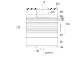
- FIG. 5 is a cross-sectional view of a light receiving element 110 shown as a reference example.
- the laminated structure is similar to the light receiving element 10 of the embodiment of the present invention shown in FIG. That is, (light-receiving layer 103 / In 0.53 Ga 0.47 As having a multiple quantum well structure of (InP substrate 101 / InP buffer layer 102 / In 0.53 Ga 0.47 As and GaAs 0.51 Sb 0.49) It has a laminated structure of diffusion concentration distribution adjusting layer 104 / InP window layer 105).
- the light receiving layer 103 is formed by stacking 200 pairs of quantum wells.
- the In 0.53 Ga 0.47 As layer 103a and the GaAs 0.51 Sb 0.49 layer 103b constituting the light receiving layer 103 both have a composition lattice-matched to InP. That is.
- a multiple quantum well structure is formed by (In 0.53 Ga 0.47 As layer 103a / GaAs 0.51 Sb 0.49 layer 103b) having a composition lattice-matched to InP.
- the conventional type 2 multiple quantum well structure of In 0.53 Ga 0.47 As and GaAs 0.51 Sb 0.49 is, without exception, a multiple quantum well structure having a lattice matching composition as shown in FIG. Was used.
- FIG. 6 is a diagram showing the wavelength dependence of the sensitivity of the light receiving element 110 shown in FIG.
- the wavelength upper limit of the light receiving sensitivity is up to 2.3 ⁇ m reflecting the type 2 multiple quantum well structure of In 0.53 Ga 0.47 As and GaAs 0.51 Sb 0.49 .
- the sensitivity rapidly decreases on the long wavelength side. This poses a problem in performing a highly reliable analysis using a plurality of absorption bands concentrated at wavelengths of 1.5 ⁇ m to 1.75 ⁇ m.
- FIG. 7 is a diagram showing the light receiving element 10 according to Embodiment 2 of the present invention.
- a pixel is formed by selectively diffusing zinc (Zn), which is a p-type impurity, from the InP window layer 5.
- the distribution of the selectively diffused Zn is from 1 ⁇ 10 18 cm ⁇ 3 to 1 ⁇ 10 19 cm ⁇ 3 on the InP window layer 5 side in the In 0.53 Ga 0.47 As diffusion concentration distribution adjusting layer 4.
- the above laminated structure is configured based on the following concept. 1. In 0.59 Ga 0.41 As3a (first semiconductor layer) in the light-receiving layer 3 The In composition x is set to 0.59 so that the band gap can be made as small as possible to receive light having a long wavelength. As a result, the upper limit of the light receiving area can be expanded to a wavelength of about 1800 nm. However, In 0.59 Ga 0.41 As3a has a large lattice constant, and by itself, it is difficult to lattice match with InP. As a result, dark current increases as the lattice defect density increases, making it difficult to detect weak light with sufficient resolution.
- the lattice defect density in the diffusion concentration distribution adjusting layer 4 and the window layer 5 grown on and in contact with the light receiving layer 3 is not increased, and the In 0.53 Ga 0.47 As diffusion concentration distribution having a good surface property.
- the adjustment layer 4 / InP window layer 5 is formed, and the dark current does not increase.
- (2) The vicinity of the upper limit wavelength (1800 nm) of the light receiving wavelength range is left to the above-described first semiconductor, In 0.59 Ga 0.41 As3a, and light corresponding to energy having a larger band gap is received.
- the first semiconductor In 0.59 Ga 0.41 As3a itself receives not only light near the upper limit of the long wavelength but also light on the shorter wavelength side.
- FIG. 8 is a diagram showing the wavelength dependence of the sensitivity of the light receiving element 10 shown in FIG. From the above (1) to (2), it can be seen that the sensitivity at the wavelength of 1.5 ⁇ m to 1.75 ⁇ m is at a high level in a substantially flat state continuously from the sensitivity on the shorter wavelength side.
- type 2 transition does not occur, and the upper limit of the wavelength at which light can be received is determined by the type 1 transition of the first semiconductor In 0.59 Ga 0.41 As3a.
- FIG. 9 is a diagram showing a flowchart of a manufacturing method of the light receiving element 10 shown in FIG.
- the multiple quantum well structure is formed by In 0.59 Ga 0.41 As3a and In 0.47 Ga 0.53 As3c, except that it is different from the first embodiment, and the other is the same as the first embodiment. .
- Example 1 A light-receiving element corresponding to the first embodiment was prototyped, and the light-receiving sensitivity and the dark current at wavelengths of 1.5 ⁇ m and 1.75 ⁇ m were evaluated.
- the test specimens are eight specimens A1 to A8 shown in Table 1. Among these test specimens, specimens A3 to A7 are examples of the present invention, and specimens A1, A2, and A8 are comparative examples.
- the first semiconductor layer 3a was made of In 0.59 Ga 0.41 As
- the second semiconductor layer 3b was made of GaAs 0.57 Sb 0.43 .
- the thickness structure is as follows.
- the light receiving sensitivity at each wavelength was measured at room temperature by the photocurrent generated when white light was incident from the back surface of the substrate through a bandpass filter corresponding to each wavelength.
- the dark current was measured at room temperature from the current flowing when no light was irradiated.
- 10 mA / cm 2 or more was regarded as defective (x), and less than 10 mA / cm 2 was evaluated as good ( ⁇ ).
- the ratio between the sensitivity of the wavelength of 1.5 ⁇ m and the sensitivity of 1.75 ⁇ m was 0.8 or more, and each sensitivity itself was 0.20 A / W or more.
- a case where the above sensitivity ratio was less than 0.8 was regarded as defective (x).
- a specimen that did not contain a defect (x) in both dark current and sensitivity was rated as good overall judgment ( ⁇ ). In particular, the case where the sensitivity itself was 1.0 A / W or higher was evaluated as excellent (().
- the sensitivity ratio was 0.8 or more, and the evaluation of dark current was good.
- Inventive Example A6 was excellent in both sensitivity and dark current, and excellent ( ⁇ ) was obtained in comprehensive judgment.
- the sensitivity ratio was poor in Comparative Example A1.
- Comparative Example A2 the sensitivity itself was low and the dark current was large.
- Comparative Example A8 the sensitivity at wavelengths of 1.5 ⁇ m and 1.75 ⁇ m was good, but the dark current was very large.
- Example 2 A light-receiving element corresponding to the second embodiment was prototyped, and the light-receiving sensitivity and dark current at wavelengths of 1.5 ⁇ m and 1.75 ⁇ m were evaluated.
- the test bodies are eight test bodies B1 to B8 shown in Table 2.
- test bodies B3 to B7 are examples of the present invention
- test bodies B1, B2, and B8 are comparative examples.
- the first semiconductor layer 3a was made of In 0.59 Ga 0.41 As
- the second semiconductor layer 3c was made of In 0.47 Ga 0.53 As.
- the thickness structure is as follows.
- Example B3 (1 nm / 1 nm) ⁇ 250 pairs: light receiving layer thickness 0.5 ⁇ m
- Example B4 (5 nm / 5 nm) ⁇ 50 pairs: light receiving layer thickness 0.5 ⁇ m
- Example B5 (5 nm / 5 nm) ⁇ 100 pair: light receiving layer thickness 1.0 ⁇ m
- Example B6 (5 nm / 5 nm) ⁇ 200 pairs: light receiving layer thickness 2.0 ⁇ m
- Example B7 (10 nm / 10 nm) ⁇ 100 pair: light receiving layer thickness 2.0 ⁇ m
- Comparative Example B1 (5 nm / 5 nm) ⁇ 40 pair: light receiving layer thickness 0.4 ⁇ m
- Comparative Example B2 (0.5 nm / 0.5 nm) ⁇ 500 pair: light receiving layer thickness 0.5 ⁇ m Comparative Example B8: (20 nm / 20 nm) ⁇ 50 pairs: light receiving layer thickness 2.0 ⁇ m In the test, light receiving sensitivity
- the dark current 10 mA / cm 2 or more was judged as poor (x), and less than 10 mA / cm 2 was judged as good ( ⁇ ).
- the ratio between the sensitivity of the wavelength of 1.5 ⁇ m and the sensitivity of 1.75 ⁇ m was 0.8 or more, and each sensitivity itself was 0.20 A / W or more.
- a case where the above sensitivity ratio was less than 0.8 was regarded as defective (x).
- a specimen that did not contain a defect (x) in both dark current and sensitivity was rated as good overall judgment ( ⁇ ). In particular, the case where the sensitivity itself was 1.0 A / W or higher was evaluated as excellent (().
- the above sensitivity ratio in Invention Examples B3 to B7 was 0.8 or more, and the evaluation of dark current was also good.
- sample B6 excellent evaluation was obtained in both sensitivity and dark current, and excellent ()) was obtained in the comprehensive judgment.
- the sensitivity ratio was poor in Comparative Example B1.
- Comparative Example B2 the sensitivity itself was poor and the dark current was large.
- Comparative Example B8 the sensitivity at wavelengths of 1.5 ⁇ m and 1.75 ⁇ m was good, but the dark current was very large.
- the dark current can be lowered with a sufficiently high sensitivity in the near infrared wavelength range of 1.5 ⁇ m to 1.8 ⁇ m. For this reason, a clear image can be obtained despite a small amount of light, and it can be suitably used for a wide range of applications as well as for communication and night imaging.
Abstract
An object of the invention is to provide a light-receiving element, and the like, which has a sufficiently high sensitivity in the near infrared wavelength region of 1.5 to 1.8 µm and is capable of reducing dark current. A light-receiving element (10) according to the invention comprises of a buffer layer (2) disposed adjacent to the top of an InP substrate (1) and a light-receiving layer (3) disposed adjacent to the top of the buffer layer. The light receiving layer is formed of at least 50 pairs, with one pair being a first semiconductor layer (3a) having a band gap energy of 0.73 eV or less and a second semiconductor layer (3b) having a band gap energy greater than that of the first semiconductor layer. The first semiconductor layer (3a) and the second semiconductor layer (3b) form a strain-compensated quantum well structure and the thickness of each layer is between 1 nm and 10 nm.
Description
本発明は、受光素子およびその製造方法に関する。より具体的には、近赤外の波長域1.5μm~1.8μmにおける感度を確保した多重量子井戸構造(Multiple-Quantum Well、以下、MQWと記す。)の受光層を含む受光素子およびその製造方法に関するものである。
The present invention relates to a light receiving element and a method for manufacturing the same. More specifically, a light-receiving element including a light-receiving layer having a multiple quantum well structure (Multiple-Quantum 、 Well, hereinafter referred to as MQW) that secures sensitivity in the near-infrared wavelength region of 1.5 μm to 1.8 μm and its It relates to a manufacturing method.
III-V族化合物半導体のInP系半導体は、バンドギャップエネルギが近赤外域に対応することから、通信用、夜間撮像用などの受光素子の開発を目的に、多数の研究開発が行われている。
たとえば非特許文献1には、InP基板上に、InGaAs/GaAsSbのタイプ2のMQWを形成し、p型またはn型のエピタキシャル層によるpn接合によってカットオフ波長2.39μmのフォトダイオードが提案され、波長1.7μm~2.7μmの感度特性が示されている。
また、非特許文献2には、InGaAs5nmとGaAsSb5nmとを1ペアとして150ペア積層したタイプ2MQWの受光層を備える受光素子の波長1μm~3μmの感度特性(200K、250K、295K)が示されている。
また、特許文献1には、光通信用に、受光域の上限波長を少しだけ拡大するために、InP基板と、そのInP基板上に形成された当該InP基板の格子定数より小さい格子定数を与える組成のIn0.53Ga0.47As(第1吸収層)と、大きい格子定数を与える組成のIn0.55Ga0.45As(第2吸収層)とを受光層に含むフォトダイオードが提案されている。これによれば、受光域を波長1700nm程度にまで長波長化することができる。 InP-based semiconductors of III-V group compound semiconductors have a band gap energy corresponding to the near-infrared region, and therefore, many researches and developments have been conducted for the purpose of developing light receiving elements for communication and night imaging. .
For example, Non-PatentDocument 1 proposes a photodiode having a cut-off wavelength of 2.39 μm by forming an InGaAs / GaAsSb type 2 MQW on an InP substrate and a pn junction formed by a p-type or n-type epitaxial layer. Sensitivity characteristics with wavelengths of 1.7 μm to 2.7 μm are shown.
Non-Patent Document 2 shows the sensitivity characteristic (200K, 250K, 295K) of a wavelength of 1 μm to 3 μm of a light receiving element having a type 2 MQW light receiving layer in which 150 pairs of InGaAs 5 nm and GaAsSb 5 nm are stacked as a pair. .
Patent Document 1 gives an InP substrate and a lattice constant smaller than the lattice constant of the InP substrate formed on the InP substrate in order to slightly expand the upper limit wavelength of the light receiving region for optical communication. A photodiode including, in a light-receiving layer, In 0.53 Ga 0.47 As (first absorption layer) having a composition and In 0.55 Ga 0.45 As (second absorption layer) having a composition that provides a large lattice constant. Proposed. According to this, the light receiving area can be lengthened to a wavelength of about 1700 nm.
たとえば非特許文献1には、InP基板上に、InGaAs/GaAsSbのタイプ2のMQWを形成し、p型またはn型のエピタキシャル層によるpn接合によってカットオフ波長2.39μmのフォトダイオードが提案され、波長1.7μm~2.7μmの感度特性が示されている。
また、非特許文献2には、InGaAs5nmとGaAsSb5nmとを1ペアとして150ペア積層したタイプ2MQWの受光層を備える受光素子の波長1μm~3μmの感度特性(200K、250K、295K)が示されている。
また、特許文献1には、光通信用に、受光域の上限波長を少しだけ拡大するために、InP基板と、そのInP基板上に形成された当該InP基板の格子定数より小さい格子定数を与える組成のIn0.53Ga0.47As(第1吸収層)と、大きい格子定数を与える組成のIn0.55Ga0.45As(第2吸収層)とを受光層に含むフォトダイオードが提案されている。これによれば、受光域を波長1700nm程度にまで長波長化することができる。 InP-based semiconductors of III-V group compound semiconductors have a band gap energy corresponding to the near-infrared region, and therefore, many researches and developments have been conducted for the purpose of developing light receiving elements for communication and night imaging. .
For example, Non-Patent
しかしながら、波長1.5μm~1.8μmの範囲に物質の重要な吸収帯が集中するので、この波長1.5μm~1.8μmの範囲に十分高い感度を持ち鮮明な画像を得ることができれば、利用を促進することができる。
しかるに、上記のタイプ2のInGaAs/GaAsSbMQWでは、波長1.6μmの少し長波長付近から急に感度が低くなる(図6参照)。これは、タイプ2遷移とタイプ1遷移の双方の光電変換によって、光電流が発生することによる。この影響で、波長1.65μm付近からタイプ1遷移の寄与が小さくなる。また、温度200K~295Kで感度が測定された同じタイプ2のInGaAs/GaAsSbMQWによる受光素子においても、波長1.5μm~1.7μmの範囲の所定波長から感度が急に低下している(図6参照)。これについても、上記と同じ感度低下要因が働いていると考えられる。
また、光通信用に受光波長上限を少し高めた受光素子については、波長1.7μm~1.8μmでの感度は十分得られるが、暗電流が高い。 However, since the important absorption band of the substance is concentrated in the wavelength range of 1.5 μm to 1.8 μm, if a clear image with sufficiently high sensitivity can be obtained in this wavelength range of 1.5 μm to 1.8 μm, Use can be promoted.
However, in thetype 2 InGaAs / GaAsSbMQW, the sensitivity suddenly decreases from around a slightly long wavelength of 1.6 μm (see FIG. 6). This is because photoelectric current is generated by photoelectric conversion of both type 2 transition and type 1 transition. Due to this influence, the contribution of the type 1 transition is reduced from around the wavelength of 1.65 μm. Also, in the light receiving element of the same type 2 InGaAs / GaAsSbMQW whose sensitivity is measured at a temperature of 200 K to 295 K, the sensitivity suddenly decreases from a predetermined wavelength in the range of 1.5 μm to 1.7 μm (FIG. 6). reference). Also in this regard, it is considered that the same sensitivity reduction factor as described above works.
In addition, a light receiving element having a light receiving wavelength upper limit slightly increased for optical communication can sufficiently obtain sensitivity at a wavelength of 1.7 μm to 1.8 μm, but has a high dark current.
しかるに、上記のタイプ2のInGaAs/GaAsSbMQWでは、波長1.6μmの少し長波長付近から急に感度が低くなる(図6参照)。これは、タイプ2遷移とタイプ1遷移の双方の光電変換によって、光電流が発生することによる。この影響で、波長1.65μm付近からタイプ1遷移の寄与が小さくなる。また、温度200K~295Kで感度が測定された同じタイプ2のInGaAs/GaAsSbMQWによる受光素子においても、波長1.5μm~1.7μmの範囲の所定波長から感度が急に低下している(図6参照)。これについても、上記と同じ感度低下要因が働いていると考えられる。
また、光通信用に受光波長上限を少し高めた受光素子については、波長1.7μm~1.8μmでの感度は十分得られるが、暗電流が高い。 However, since the important absorption band of the substance is concentrated in the wavelength range of 1.5 μm to 1.8 μm, if a clear image with sufficiently high sensitivity can be obtained in this wavelength range of 1.5 μm to 1.8 μm, Use can be promoted.
However, in the
In addition, a light receiving element having a light receiving wavelength upper limit slightly increased for optical communication can sufficiently obtain sensitivity at a wavelength of 1.7 μm to 1.8 μm, but has a high dark current.
本発明は、近赤外の波長域1.5μm~1.8μmに安定して十分高い感度をもち、暗電流を低くできる受光素子およびその製造方法を提供することを目的とする。
An object of the present invention is to provide a light-receiving element that can stably have a sufficiently high sensitivity in the near-infrared wavelength region of 1.5 μm to 1.8 μm and can reduce the dark current, and a method for manufacturing the same.
本発明の受光素子は、InP基板上に形成されたIII-V族化合物半導体による受光素子である。この受光素子は、InP基板上に接して位置するバッファ層と、バッファ層上に接して位置する受光層とを備える。この受光層が、バンドギャップエネルギ0.73eV以下の第1の半導体層と、該第1の半導体層のバンドギャップエネルギよりも大きいバンドギャップエネルギを持つ第2の半導体層とを交互に積層して50ペア以上含み、第1の半導体層および第2の半導体層が歪補償量子井戸構造を形成し、該第1の半導体層および第2の半導体層の厚みが両方とも1nm以上10nm以下であることを特徴とする。
The light receiving element of the present invention is a light receiving element made of a III-V group compound semiconductor formed on an InP substrate. The light receiving element includes a buffer layer positioned in contact with the InP substrate and a light receiving layer positioned in contact with the buffer layer. The light receiving layer is formed by alternately laminating a first semiconductor layer having a band gap energy of 0.73 eV or less and a second semiconductor layer having a band gap energy larger than the band gap energy of the first semiconductor layer. 50 pairs or more are included, the first semiconductor layer and the second semiconductor layer form a strain compensation quantum well structure, and the thicknesses of the first semiconductor layer and the second semiconductor layer are both 1 nm or more and 10 nm or less. It is characterized by.
上記において第1の半導体層のバンドギャップエネルギを0.73eV以下とすることによって、第1の半導体層内におけるタイプ1の遷移に基づいて波長1.7μm~1.8μmで高い受光感度を得ることができる。ここで、バンドギャップエネルギと格子定数との反比例の関係から、上記の第1の半導体層はInP基板に比べて格子定数が大きく、一方第2の半導体層は格子定数が小さいため、前者には圧縮応力がまた後者には引張応力が分布して、両者は歪補償量子井戸構造を形成する。第1の半導体層/第2の半導体層を50ペア以上として各半導体層の厚みを1nm以上10nm以下とすることで、格子不整合による圧縮歪と引張歪とを均衡させてマクロ的に歪の影響を小さくすることができる。この歪の蓄積が回避されることで、結晶性が向上して暗電流の増大を防止することができる。すなわち波長1.5μm~1.8μm付近で高い受光感度を持ちながら暗電流を低く抑えることができる。
In the above, by setting the band gap energy of the first semiconductor layer to 0.73 eV or less, high light receiving sensitivity can be obtained at a wavelength of 1.7 μm to 1.8 μm based on the type 1 transition in the first semiconductor layer. Can do. Here, because of the inversely proportional relationship between the band gap energy and the lattice constant, the first semiconductor layer has a larger lattice constant than the InP substrate, while the second semiconductor layer has a smaller lattice constant. Compressive stress and tensile stress are distributed in the latter, and both form a strain compensated quantum well structure. The first semiconductor layer / second semiconductor layer is 50 pairs or more, and the thickness of each semiconductor layer is 1 nm or more and 10 nm or less, so that the compressive strain and tensile strain due to lattice mismatch are balanced and the strain is macroscopically. The influence can be reduced. By avoiding the accumulation of this strain, the crystallinity can be improved and an increase in dark current can be prevented. That is, dark current can be kept low while having high light receiving sensitivity in the vicinity of a wavelength of 1.5 μm to 1.8 μm.
波長1.5μmおよび1.75μmを含む波長域に受光感度を有する受光素子であって、波長1.5μmの受光感度と波長1.75μmの受光感度との比を、0.8以上1.2以下とすることができる。
これによって、物質の重要な吸収帯が集中する波長域に十分大きな感度を持つ受光素子を得ることができる。この受光素子は、MCT(HgCdTe)等のように冷却を必要とせず、室温使用を前提とするので、使いやすく小型なため通信用、夜間撮像用のみならず広い用途に手軽に使用できる。 A light receiving element having light receiving sensitivity in a wavelength region including wavelengths of 1.5 μm and 1.75 μm, wherein a ratio of a light receiving sensitivity of a wavelength of 1.5 μm to a light receiving sensitivity of a wavelength of 1.75 μm is 0.8 or more and 1.2. It can be as follows.
As a result, a light receiving element having a sufficiently large sensitivity in a wavelength region where important absorption bands of substances are concentrated can be obtained. This light receiving element does not require cooling unlike MCT (HgCdTe) or the like, and is premised on use at room temperature. Therefore, since it is easy to use and small, it can be easily used not only for communication and for night imaging.
第1の半導体層および第2の半導体層を、(1)タイプ2の多重量子井戸構造を形成するか、または(2)組成が異なる同じ化合物半導体とすることができる。
これによって、歪補償量子井戸構造を、(1)タイプ2の多重量子井戸構造としてもよいし、または(2)組成が異なる、たとえばInGaAsを用いてもよい。(1)前者の場合、タイプ1の遷移だけでなくタイプ2の遷移によっても波長1.7μm~1.8μmの光を受光することができる。(2)後者の場合は、タイプ1の多重量子井戸構造に限定して、物質にとって重要な吸収帯が集中する波長1.5μm~1.8μm付近で高い受光感度を持ちながら暗電流を低く抑えることができる。この場合、タイプ2の遷移は生じないので、波長1.8μmを超える範囲に受光感度はない。しかし、たとえば歪補償量子井戸構造内にSbなどの取り扱いが難しい元素を含まないことから良好な結晶性の薄膜を得ることができる。 The first semiconductor layer and the second semiconductor layer can be (1) atype 2 multiple quantum well structure or (2) the same compound semiconductor having a different composition.
Accordingly, the strain compensation quantum well structure may be (1) atype 2 multiple quantum well structure, or (2) a composition having a different composition, for example, InGaAs may be used. (1) In the former case, light having a wavelength of 1.7 μm to 1.8 μm can be received not only by the type 1 transition but also by the type 2 transition. (2) In the latter case, limiting to the type 1 multiple quantum well structure, the dark current is kept low while having high light receiving sensitivity in the vicinity of the wavelength of 1.5 μm to 1.8 μm where the absorption bands important for the substance are concentrated. be able to. In this case, since type 2 transition does not occur, there is no light receiving sensitivity in a range exceeding the wavelength of 1.8 μm. However, for example, since an element that is difficult to handle such as Sb is not included in the strain compensation quantum well structure, a thin film having good crystallinity can be obtained.
これによって、歪補償量子井戸構造を、(1)タイプ2の多重量子井戸構造としてもよいし、または(2)組成が異なる、たとえばInGaAsを用いてもよい。(1)前者の場合、タイプ1の遷移だけでなくタイプ2の遷移によっても波長1.7μm~1.8μmの光を受光することができる。(2)後者の場合は、タイプ1の多重量子井戸構造に限定して、物質にとって重要な吸収帯が集中する波長1.5μm~1.8μm付近で高い受光感度を持ちながら暗電流を低く抑えることができる。この場合、タイプ2の遷移は生じないので、波長1.8μmを超える範囲に受光感度はない。しかし、たとえば歪補償量子井戸構造内にSbなどの取り扱いが難しい元素を含まないことから良好な結晶性の薄膜を得ることができる。 The first semiconductor layer and the second semiconductor layer can be (1) a
Accordingly, the strain compensation quantum well structure may be (1) a
第1の半導体層の受光層における合計膜厚を、0.5μm以上とするのがよい。
これによって、とくに波長1.75μm付近の上限における感度を確保することができる。この波長1.75μm付近の受光は、第1の半導体層のバルクでのタイプ1遷移によるので、合計膜厚を0.5μm以上とすることで感度を確保できる。 The total film thickness in the light receiving layer of the first semiconductor layer is preferably 0.5 μm or more.
As a result, it is possible to ensure sensitivity especially at the upper limit near the wavelength of 1.75 μm. The light reception in the vicinity of the wavelength of 1.75 μm is due to thetype 1 transition in the bulk of the first semiconductor layer. Therefore, the sensitivity can be ensured by setting the total film thickness to 0.5 μm or more.
これによって、とくに波長1.75μm付近の上限における感度を確保することができる。この波長1.75μm付近の受光は、第1の半導体層のバルクでのタイプ1遷移によるので、合計膜厚を0.5μm以上とすることで感度を確保できる。 The total film thickness in the light receiving layer of the first semiconductor layer is preferably 0.5 μm or more.
As a result, it is possible to ensure sensitivity especially at the upper limit near the wavelength of 1.75 μm. The light reception in the vicinity of the wavelength of 1.75 μm is due to the
バッファ層のバンドギャップエネルギを、第1の半導体層および第2の半導体層のいずれのバンドギャップエネルギよりも大きくするのがよい。
これによって、基板裏面入射の場合(画素を二次元アレイ化では必須)、光がバッファ層で吸収されることを防ぐことができる。またInP(基板)のバンドギャップエネルギは1.27eVであり、当然、今問題にしている波長域の光が吸収されるおそれはない。 The band gap energy of the buffer layer is preferably larger than the band gap energy of either the first semiconductor layer or the second semiconductor layer.
This prevents light from being absorbed by the buffer layer in the case of substrate backside incidence (necessary for two-dimensional array of pixels). Further, the band gap energy of InP (substrate) is 1.27 eV, and naturally, there is no possibility of absorbing light in the wavelength region currently in question.
第1の半導体層をInxGa1-xAs(0.56≦x≦0.68)とすることができる。
これによって、タイプ1の遷移で波長1.7μm~1.8μmまで確実に受光できる第1の半導体層を得ることができる。 The first semiconductor layer can be In x Ga 1-x As (0.56 ≦ x ≦ 0.68).
This makes it possible to obtain a first semiconductor layer that can reliably receive light with a wavelength of 1.7 μm to 1.8 μm in thetype 1 transition.
これによって、タイプ1の遷移で波長1.7μm~1.8μmまで確実に受光できる第1の半導体層を得ることができる。 The first semiconductor layer can be In x Ga 1-x As (0.56 ≦ x ≦ 0.68).
This makes it possible to obtain a first semiconductor layer that can reliably receive light with a wavelength of 1.7 μm to 1.8 μm in the
第2の半導体層を、InyGa1-yAs(0.38≦y≦0.50)とすることができる。
これによって、第2の半導体層の格子定数をInPより小さくして、InPより大きい格子定数の第1の半導体層との組み合わせにより、歪補償量子井戸構造を容易に形成することができる。この結果、窓層まで含めてエピタキシャル層全体の結晶性を良好にすることができ、暗電流を減らすことができる。この第2の半導体層も、当然、タイプ1遷移によって受光可能であるが、受光可能な波長上限は、1.7μmよりも短い範囲となる。 The second semiconductor layer can be In y Ga 1-y As (0.38 ≦ y ≦ 0.50).
Thus, the strain compensation quantum well structure can be easily formed by combining the second semiconductor layer with a lattice constant smaller than InP and the first semiconductor layer having a lattice constant larger than InP. As a result, the crystallinity of the entire epitaxial layer including the window layer can be improved, and the dark current can be reduced. Naturally, this second semiconductor layer can also receive light by thetype 1 transition, but the upper limit of the wavelength that can be received is in a range shorter than 1.7 μm.
これによって、第2の半導体層の格子定数をInPより小さくして、InPより大きい格子定数の第1の半導体層との組み合わせにより、歪補償量子井戸構造を容易に形成することができる。この結果、窓層まで含めてエピタキシャル層全体の結晶性を良好にすることができ、暗電流を減らすことができる。この第2の半導体層も、当然、タイプ1遷移によって受光可能であるが、受光可能な波長上限は、1.7μmよりも短い範囲となる。 The second semiconductor layer can be In y Ga 1-y As (0.38 ≦ y ≦ 0.50).
Thus, the strain compensation quantum well structure can be easily formed by combining the second semiconductor layer with a lattice constant smaller than InP and the first semiconductor layer having a lattice constant larger than InP. As a result, the crystallinity of the entire epitaxial layer including the window layer can be improved, and the dark current can be reduced. Naturally, this second semiconductor layer can also receive light by the
第2の半導体層をGaAszSb1-z(0.54≦z≦0.66)とすることができる。
この場合も第2の半導体層の格子定数をInPより小さくして、InPより大きい格子定数の第1の半導体層との組み合わせにより、歪補償量子井戸構造を容易に形成することができる。この場合、取り扱いの難しいSbを減らすことになるので、エピタキシャル層全体の結晶性を高め、かつ暗電流を抑制する上で好ましい。この場合、タイプ2の遷移が可能であり、波長1.8μm以上の長波長側だけでなく、焦点となっている波長1.7μm~1.8μmの波長域の光もタイプ2の遷移により受光することができる。すなわち、第1の半導体層によるタイプ1の遷移による波長1.7μm~1.8μmの光の受光だけでなく、タイプ2の遷移によっても波長1.7μm~1.8μmの光の受光ができる。 The second semiconductor layer can be GaAs z Sb 1-z (0.54 ≦ z ≦ 0.66).
Also in this case, the strain compensation quantum well structure can be easily formed by combining the second semiconductor layer with a lattice constant smaller than that of InP and the first semiconductor layer having a lattice constant larger than that of InP. In this case, since Sb that is difficult to handle is reduced, it is preferable for enhancing the crystallinity of the entire epitaxial layer and suppressing dark current. In this case,type 2 transition is possible, and not only the long wavelength side with a wavelength of 1.8 μm or longer, but also light in the wavelength range of 1.7 μm to 1.8 μm, which is the focal point, is received by the type 2 transition. can do. That is, not only light having a wavelength of 1.7 μm to 1.8 μm due to the type 1 transition by the first semiconductor layer but also light having a wavelength of 1.7 μm to 1.8 μm can be received by the type 2 transition.
この場合も第2の半導体層の格子定数をInPより小さくして、InPより大きい格子定数の第1の半導体層との組み合わせにより、歪補償量子井戸構造を容易に形成することができる。この場合、取り扱いの難しいSbを減らすことになるので、エピタキシャル層全体の結晶性を高め、かつ暗電流を抑制する上で好ましい。この場合、タイプ2の遷移が可能であり、波長1.8μm以上の長波長側だけでなく、焦点となっている波長1.7μm~1.8μmの波長域の光もタイプ2の遷移により受光することができる。すなわち、第1の半導体層によるタイプ1の遷移による波長1.7μm~1.8μmの光の受光だけでなく、タイプ2の遷移によっても波長1.7μm~1.8μmの光の受光ができる。 The second semiconductor layer can be GaAs z Sb 1-z (0.54 ≦ z ≦ 0.66).
Also in this case, the strain compensation quantum well structure can be easily formed by combining the second semiconductor layer with a lattice constant smaller than that of InP and the first semiconductor layer having a lattice constant larger than that of InP. In this case, since Sb that is difficult to handle is reduced, it is preferable for enhancing the crystallinity of the entire epitaxial layer and suppressing dark current. In this case,
InP基板上の受光層を含むエピタキシャル層の表層にInP窓層を備え、バッファ層の底面とInP窓層表面との間に、再成長界面を持たないようにするのがよい。
これによって、一貫して同じ成膜室(全有機金属気相成長法による成膜室)において受光素子の心臓部である半導体エピタキシャル層を形成することができる。ここで、全有機金属気相成長法とは、有機物と金属との化合物で構成される有機金属原料を気相成長用原料のすべてに用いる成長方法のことをいい、全有機MOVPE法と記す。この結果、再成長界面における高濃度のO、Cなどによる汚染を防止することができる。この結果、暗電流を低くすることができる。また、一貫して同じ成膜室で成長できるので、高い製造能率を得ることができる。 It is preferable to provide an InP window layer on the surface layer of the epitaxial layer including the light receiving layer on the InP substrate so that there is no regrowth interface between the bottom surface of the buffer layer and the surface of the InP window layer.
Thus, it is possible to consistently form a semiconductor epitaxial layer that is the heart of the light receiving element in the same film formation chamber (deposition chamber formed by all metal organic vapor phase epitaxy). Here, the all-organic metal vapor phase growth method refers to a growth method in which an organic metal raw material composed of a compound of an organic substance and a metal is used for all the raw materials for vapor phase growth, and is referred to as a total organic MOVPE method. As a result, it is possible to prevent contamination due to high concentrations of O, C, etc. at the regrowth interface. As a result, the dark current can be lowered. In addition, since it can be grown in the same film forming chamber consistently, high production efficiency can be obtained.
バッファ層がPを含むことができる。
バッファ層にPを含む場合としてInPバッファ層、InGaAsPバッファ層などがある。これらのバッファ層は良好な結晶性の薄膜を成長しやすい。このためこのバッファ層上に接して成長する受光層(第1および第2の半導体層)の結晶性も良好にでき、その結果、暗電流を低くすることができる。 The buffer layer can include P.
Examples of cases where P is contained in the buffer layer include an InP buffer layer and an InGaAsP buffer layer. These buffer layers are easy to grow a good crystalline thin film. For this reason, the crystallinity of the light receiving layer (first and second semiconductor layers) grown in contact with the buffer layer can be improved, and as a result, the dark current can be lowered.
InP基板の裏面を入射面とするための基板裏面入射構造を備えることができる。
ここで、基板裏面側から光を入射する構造、とは、(1)エピタキシャル層表面側における画素電極に設けた接合用バンプ(読み出し回路がエピタキシャル層表面側を覆うことになる)、(2)基板裏面側に設けた反射防止用の膜(AR膜)、(3)基板裏面入射とせざるを得ない、基本単位となる受光素子(画素)の二次元配列の態様、などをいう(その他の構造例については後で言及する)。
上記の基板裏面入射構造を備えることで、低い暗電流を維持し、高い感度を確保しながら二次元アレイ化された画素を有する受光素子を製造することができる。 A substrate back surface incident structure for making the back surface of the InP substrate the incident surface can be provided.
Here, the structure in which light is incident from the back side of the substrate means (1) bonding bumps provided on the pixel electrode on the surface side of the epitaxial layer (the readout circuit covers the surface side of the epitaxial layer), (2) An anti-reflection film (AR film) provided on the back side of the substrate, (3) a two-dimensional arrangement of light receiving elements (pixels) as a basic unit, which must be incident on the back side of the substrate (others) An example structure will be described later).
By providing the substrate backside incident structure described above, it is possible to manufacture a light receiving element having two-dimensionally arrayed pixels while maintaining a low dark current and ensuring high sensitivity.
選択拡散によって導入された不純物の先端部にpn接合を備え、受光層のInP基板と反対側の面である上面に接するIII-V族化合物半導体の拡散濃度分布調整層と、その拡散濃度分布調整層上に接するPを含む窓層とを備え、拡散濃度分布調整層のバンドギャップエネルギを窓層のバンドギャップエネルギよりも小さくするのがよい。
これによって、拡散濃度分布調整層の電気抵抗が大きいと感度の低下や画像形成の遅れ等が生じるが、バンドギャップエネルギが窓層よりも小さい材料を用いることで電気抵抗の増大を防ぐことができる。また、画素形成において、結晶性を良好にできる選択拡散を用いながら、選択拡散によって過度に高濃度の不純物を受光層内に導入して歪補償量子井戸構造の結晶性がその不純物で害されるのを防止することができる。この場合、拡散濃度分布調整層内で不純物濃度は急峻に低下する分布形態とするのがよい。 III-V group compound semiconductor diffusion concentration distribution adjustment layer having a pn junction at the front end of the impurity introduced by selective diffusion and in contact with the upper surface of the light receiving layer opposite to the InP substrate, and adjustment of the diffusion concentration distribution thereof And a window layer containing P in contact with the layer, and the band gap energy of the diffusion concentration distribution adjusting layer is preferably made smaller than the band gap energy of the window layer.
As a result, if the electric resistance of the diffusion concentration distribution adjusting layer is large, the sensitivity is lowered and the image formation is delayed, but an increase in electric resistance can be prevented by using a material whose band gap energy is smaller than that of the window layer. . In addition, in the pixel formation, while using selective diffusion that can improve the crystallinity, excessively high-concentration impurities are introduced into the light receiving layer by selective diffusion, and the crystallinity of the strain compensation quantum well structure is damaged by the impurities. Can be prevented. In this case, it is preferable to adopt a distribution form in which the impurity concentration sharply decreases in the diffusion concentration distribution adjusting layer.
本発明の受光素子の製造方法では、InP基板上に形成されたIII-V族化合物半導体による受光素子を製造する。この製造方法は、InP基板上にバッファ層を形成する工程と、バッファ層上に、バンドギャップ0.73eV以下の第1の半導体層と、該第1の半導体層よりも大きいバンドギャップを持つ第2の半導体層とを、該第1および第2の半導体層の両方ともに厚み1nm以上10nm以下で、交互に50ペア以上積層して、多重量子井戸構造の受光層を形成する工程とを備える。そして、多重量子井戸構造の受光層の形成工程では、全有機金属気相成長法によって、成長温度または基板温度600℃以下で成長することを特徴とする。
In the method for manufacturing a light receiving element of the present invention, a light receiving element made of a III-V group compound semiconductor formed on an InP substrate is manufactured. This manufacturing method includes a step of forming a buffer layer on an InP substrate, a first semiconductor layer having a band gap of 0.73 eV or less on the buffer layer, and a first semiconductor layer having a band gap larger than that of the first semiconductor layer. And forming a light-receiving layer having a multiple quantum well structure by alternately stacking 50 pairs or more of both the first and second semiconductor layers with a thickness of 1 nm to 10 nm. In the step of forming the light-receiving layer having the multiple quantum well structure, the growth is performed at a growth temperature or a substrate temperature of 600 ° C. or less by a total organometallic vapor phase growth method.
上述のように受光層は歪補償量子井戸構造であり、良好な結晶性を得られるか否かが重要である。全有機金属気相成長法では、成長温度または基板温度を低くできるので、成長後に冷却する際に温度差に起因する熱膨張によって結晶性が劣化する程度を低く抑えることができる。
上記の成長温度または基板温度は、基板表面温度を赤外線カメラおよび赤外線分光器を含むパイロメータでモニタしており、そのモニタされている基板表面温度をいう。したがって、基板表面温度ではあるが、厳密には、基板上に成膜がなされている状態の、エピタキシャル層表面の温度である。基板温度、成長温度、成膜温度など、呼称は各種あるが、いずれも上記のモニタされている温度をさす。 As described above, the light receiving layer has a strain compensated quantum well structure, and it is important whether or not good crystallinity can be obtained. In the all-organic metal vapor phase growth method, the growth temperature or the substrate temperature can be lowered, so that the degree of crystallinity degradation due to thermal expansion caused by the temperature difference can be kept low when cooling after growth.
The growth temperature or the substrate temperature is a substrate surface temperature monitored by a pyrometer including an infrared camera and an infrared spectrometer. Accordingly, although it is the substrate surface temperature, strictly speaking, it is the temperature of the epitaxial layer surface in a state where a film is formed on the substrate. There are various names such as a substrate temperature, a growth temperature, and a film formation temperature, and all refer to the monitored temperatures.
受光層の上にIII-V族化合物半導体層を形成する工程を備え、受光層を形成し始めるときからIII-V族化合物半導体層を形成し終わるときまで、全有機金属気相成長法によって同じ成膜室内で成長するのがよい。
これによって、一貫して全有機金属気相成長(全有機MOVPE法)による成膜室において受光素子の心臓部である半導体エピタキシャル層を形成することができる。この結果、再成長界面における高濃度のO、Cなどによる汚染を防止することができる。この結果、暗電流を低くすることができる。また、一貫して同じ成膜室で成長できるので、高い製造能率を得ることができる。 A step of forming a group III-V compound semiconductor layer on the light-receiving layer, and from the start of forming the light-receiving layer until the end of the formation of the group III-V compound semiconductor layer, the same by the all-organic metal vapor phase epitaxy method It is preferable to grow in the deposition chamber.
Thus, it is possible to consistently form a semiconductor epitaxial layer which is the heart of the light receiving element in a film forming chamber by all metal organic vapor phase epitaxy (all organic MOVPE method). As a result, it is possible to prevent contamination due to high concentrations of O, C, etc. at the regrowth interface. As a result, the dark current can be lowered. In addition, since it can be grown in the same film forming chamber consistently, high production efficiency can be obtained.
本発明の受光素子等によれば、近赤外の波長域1.5μm~1.8μmに安定して十分高い感度をもち、暗電流を低くすることができる。
According to the light receiving element of the present invention, the dark current can be lowered with a sufficiently high sensitivity stably in the near infrared wavelength range of 1.5 μm to 1.8 μm.
1 InP基板、2 InPバッファ層、3 MQW受光層、3a In0.59Ga0.41As(第1の半導体層)、3b GaAs0.57Sb.43(第2の半導体層)、3c In0.47Ga0.53As(第2の半導体層)、4 InGaAs層(拡散濃度分布調整層)、5 InP窓層、6 p型領域、10 受光素子、11 p側電極(画素電極)、12 グランド電極(n側電極)、16 MQWとInGaAs層との界面、17 InGaAs層とInP窓層との界面、35 AR(反射防止)膜、36 選択拡散マスクパターン、60 全有機金属気相成長法の成膜装置、61 赤外線温度モニタ装置、63 反応室、65 石英管、66 基板テーブル、66h ヒータ、69 反応室の窓。
1 InP substrate, 2 InP buffer layer, 3 MQW light receiving layer, 3a In 0.59 Ga 0.41 As (first semiconductor layer), 3b GaAs 0.57 S b. 43 (second semiconductor layer), 3c In 0.47 Ga 0.53 As (second semiconductor layer), 4 InGaAs layer (diffusion concentration distribution adjusting layer), 5 InP window layer, 6 p-type region, 10 light reception Element, 11 p-side electrode (pixel electrode), 12 ground electrode (n-side electrode), 16 interface between MQW and InGaAs layer, 17 interface between InGaAs layer and InP window layer, 35 AR (antireflection) film, 36 selection Diffusion mask pattern, 60 All metal organic vapor phase deposition apparatus, 61 Infrared temperature monitor, 63 reaction chamber, 65 quartz tube, 66 substrate table, 66h heater, 69 reaction chamber window.
(実施の形態1)
図1は、本発明の実施の形態1における受光素子10を示す断面図である。図1によれば、受光素子10は、InP基板1の上に次の構成のIII-V族化合物半導体積層構造を有する。
(InP基板1/InPバッファ層2/In0.59Ga0.41As(第1の半導体層)3aとGaAs0.57Sb0.43(第2の半導体層)3bとの多重量子井戸構造による受光層3/InGaAs拡散濃度分布調整層4/InP窓層5)
InP窓層5から多重量子井戸構造の受光層3の近くにまでp型領域6が位置している。このp型領域6は、SiN膜の選択拡散マスクパターン36の開口部から、p型不純物のZnが選択拡散されることで形成される。受光素子10の周縁部の内側に、平面的に周囲限定されて拡散導入され、受光部が周縁部の内側に形成されることは、上記SiN膜の選択拡散マスクパターン36を用いて拡散することによって実現される。 (Embodiment 1)
FIG. 1 is a cross-sectional view showing alight receiving element 10 according to Embodiment 1 of the present invention. According to FIG. 1, the light receiving element 10 has a III-V compound semiconductor laminated structure of the following configuration on the InP substrate 1.
(InP substrate 1 / InP buffer layer 2 / In 0.59 Ga 0.41 As (first semiconductor layer) 3a and GaAs 0.57 Sb 0.43 (second semiconductor layer) 3b multiple quantum well structure Light receiving layer 3 / InGaAs diffusion concentration distribution adjusting layer 4 / InP window layer 5)
A p-type region 6 is located from the InP window layer 5 to the vicinity of the light-receiving layer 3 having a multiple quantum well structure. The p-type region 6 is formed by selectively diffusing Zn of the p-type impurity from the opening of the selective diffusion mask pattern 36 of the SiN film. It is diffused by using the selective diffusion mask pattern 36 of the SiN film that the periphery is limited in a plane and is introduced into the inside of the periphery of the light receiving element 10 and the light receiving part is formed inside the periphery. It is realized by.
図1は、本発明の実施の形態1における受光素子10を示す断面図である。図1によれば、受光素子10は、InP基板1の上に次の構成のIII-V族化合物半導体積層構造を有する。
(InP基板1/InPバッファ層2/In0.59Ga0.41As(第1の半導体層)3aとGaAs0.57Sb0.43(第2の半導体層)3bとの多重量子井戸構造による受光層3/InGaAs拡散濃度分布調整層4/InP窓層5)
InP窓層5から多重量子井戸構造の受光層3の近くにまでp型領域6が位置している。このp型領域6は、SiN膜の選択拡散マスクパターン36の開口部から、p型不純物のZnが選択拡散されることで形成される。受光素子10の周縁部の内側に、平面的に周囲限定されて拡散導入され、受光部が周縁部の内側に形成されることは、上記SiN膜の選択拡散マスクパターン36を用いて拡散することによって実現される。 (Embodiment 1)
FIG. 1 is a cross-sectional view showing a
(
A p-
p型領域6にはAuZnによるp側電極11が、またInP基板1の裏面にはAuGeNiのn側電極12が、それぞれオーミック接触するように設けられている。この場合、InP基板1にはn型不純物がドープされ、所定レベルの導電性を確保されている。
光は、InP基板1の裏面から入射される。入射光の反射を防止するためにSiON等によるAR(Anti-reflection)膜35がInP基板1の裏面を被覆する。このInP基板1の裏面に配置されたAR膜35は、基板側から入射するための構造といってよい。さらに画素電極(p側電極)11を、半導体積層体の頂面の端ではなく中央寄りまたは中央付近に配置することは、半導体積層体の頂面から光を入射させないことを意味しており、半導体基板の裏面側から光を入射するための構造ということができる。さらに、図示はしていないが、読み出し回路の読み出し電極と接合するための接合バンプを画素電極に配置した構造も、半導体基板の裏面入射のための構造ということができる。読み出し回路が、画素側全体を覆うことになるからである。同じく図示はしていないが、グランド電極と画素電極の両方を、エピタキシャル層表面側に延在させる構造も、間違いなく、基板裏面入射のための構造である。これら例示した構造に限らず、基板裏面入射とされた受光素子では、半導体基板の裏面入射のための構造は、必ず存在する。
また画素Pの二次元配列自体、読み出し回路との接続に用いられるフリップフロップ接合方式のため、基板裏面入射は必然であり、上記の基板裏面から入射するための構造である。 A p-side electrode 11 made of AuZn is provided in the p-type region 6, and an n-side electrode 12 made of AuGeNi is provided in ohmic contact with the back surface of the InP substrate 1. In this case, the InP substrate 1 is doped with n-type impurities to ensure a predetermined level of conductivity.
Light enters from the back surface of theInP substrate 1. In order to prevent reflection of incident light, an AR (Anti-reflection) film 35 made of SiON or the like covers the back surface of the InP substrate 1. The AR film 35 disposed on the back surface of the InP substrate 1 may be regarded as a structure for entering from the substrate side. Furthermore, disposing the pixel electrode (p-side electrode) 11 near or near the center instead of the end of the top surface of the semiconductor stacked body means that light does not enter from the top surface of the semiconductor stacked body, It can be said that the light is incident from the back side of the semiconductor substrate. Further, although not shown, a structure in which bonding bumps for bonding to the reading electrodes of the reading circuit are arranged on the pixel electrodes can also be referred to as a structure for incident on the back surface of the semiconductor substrate. This is because the readout circuit covers the entire pixel side. Although not shown in the figure, the structure in which both the ground electrode and the pixel electrode extend to the surface side of the epitaxial layer is definitely a structure for incident on the back surface of the substrate. The structure for the back surface incidence of the semiconductor substrate necessarily exists in the light receiving element that is not limited to these exemplified structures and is incident on the back surface of the substrate.
Further, since the two-dimensional array of pixels P itself is a flip-flop junction system used for connection with the readout circuit, the substrate back surface incidence is inevitable, and the above structure is for entering from the substrate back surface.
光は、InP基板1の裏面から入射される。入射光の反射を防止するためにSiON等によるAR(Anti-reflection)膜35がInP基板1の裏面を被覆する。このInP基板1の裏面に配置されたAR膜35は、基板側から入射するための構造といってよい。さらに画素電極(p側電極)11を、半導体積層体の頂面の端ではなく中央寄りまたは中央付近に配置することは、半導体積層体の頂面から光を入射させないことを意味しており、半導体基板の裏面側から光を入射するための構造ということができる。さらに、図示はしていないが、読み出し回路の読み出し電極と接合するための接合バンプを画素電極に配置した構造も、半導体基板の裏面入射のための構造ということができる。読み出し回路が、画素側全体を覆うことになるからである。同じく図示はしていないが、グランド電極と画素電極の両方を、エピタキシャル層表面側に延在させる構造も、間違いなく、基板裏面入射のための構造である。これら例示した構造に限らず、基板裏面入射とされた受光素子では、半導体基板の裏面入射のための構造は、必ず存在する。
また画素Pの二次元配列自体、読み出し回路との接続に用いられるフリップフロップ接合方式のため、基板裏面入射は必然であり、上記の基板裏面から入射するための構造である。 A p-
Light enters from the back surface of the
Further, since the two-dimensional array of pixels P itself is a flip-flop junction system used for connection with the readout circuit, the substrate back surface incidence is inevitable, and the above structure is for entering from the substrate back surface.
上記のp型領域6の境界フロントに対応する位置にpn接合が形成され、上記のp側電極11およびn側電極12間に逆バイアス電圧を印加することにより、受光層3のn型不純物濃度が低い側(n型不純物バックグラウンド)により広く空乏層を生じる。多重量子井戸構造の受光層3におけるバックグラウンド不純物濃度は、n型不純物濃度(キャリア濃度)で5×1015cm-3程度またはそれ以下である。そして、pn接合の位置は、多重量子井戸の受光層3のバックグラウンド不純物濃度(n型キャリア濃度)と、p型不純物のZnの濃度プロファイルとの交点で決まる。
拡散濃度分布調整層4内では、InP窓層5の表面から選択拡散されたp型不純物の濃度が、InP窓層側における高濃度領域から受光層側にかけて急峻に低下している。このため、受光層3内では、Zn濃度は5×1016cm-3以下の不純物濃度を容易に実現することができる。 A pn junction is formed at a position corresponding to the boundary front of the p-type region 6, and a reverse bias voltage is applied between the p-side electrode 11 and the n-side electrode 12. The lower side (n-type impurity background) produces a wider depletion layer. The background impurity concentration in the light-receiving layer 3 having the multiple quantum well structure is about 5 × 10 15 cm −3 or less in terms of n-type impurity concentration (carrier concentration). The position of the pn junction is determined by the intersection of the background impurity concentration (n-type carrier concentration) of the light-receiving layer 3 of the multiple quantum well and the Zn concentration profile of the p-type impurity.
In the diffusion concentration distribution adjusting layer 4, the concentration of the p-type impurity selectively diffused from the surface of theInP window layer 5 sharply decreases from the high concentration region on the InP window layer side to the light receiving layer side. Therefore, in the light receiving layer 3, an impurity concentration of 5 × 10 16 cm −3 or less can be easily realized.
拡散濃度分布調整層4内では、InP窓層5の表面から選択拡散されたp型不純物の濃度が、InP窓層側における高濃度領域から受光層側にかけて急峻に低下している。このため、受光層3内では、Zn濃度は5×1016cm-3以下の不純物濃度を容易に実現することができる。 A pn junction is formed at a position corresponding to the boundary front of the p-
In the diffusion concentration distribution adjusting layer 4, the concentration of the p-type impurity selectively diffused from the surface of the
本発明が対象とする受光素子10は、近赤外域からその長波長側に受光感度を有することを追求するので、窓層には、受光層3のバンドギャップエネルギより大きいバンドギャップエネルギの材料を用いるのが好ましい。このため、窓層には、通常、受光層よりもバンドギャップエネルギが大きく、格子整合の良い材料であるInPが用いられる。InPとほぼ同じバンドギャップエネルギを有するInAlAsを用いてもよい。
Since the light receiving element 10 targeted by the present invention seeks to have light receiving sensitivity from the near infrared region to the long wavelength side, a material having a band gap energy larger than the band gap energy of the light receiving layer 3 is used for the window layer. It is preferable to use it. For this reason, InP, which is a material having a band gap energy larger than that of the light receiving layer and having a good lattice matching, is usually used for the window layer. InAlAs having substantially the same band gap energy as InP may be used.
(実施の形態1におけるポイント)
本実施の形態における特徴は、次の点にある。
(1)受光層3内の第1の半導体層3aのInP格子整合のIn組成を、0.53よりも大きく高めてIn0.59Ga0.41Asとすることで、バンドギャップエネルギを0.73eV以下を実現した。このため、第1の半導体層3aにおけるタイプ1の遷移によって、波長1.7μm~1.8μmにおける受光感度を高めることができる。
In0.59Ga0.41Asは、InPに格子整合する組成In0.53Ga0.47Asに比べてIn組成が格段に高く、従って、InPよりも格子定数は大きい。このため、第1の半導体層3aには圧縮応力が分布する。
(2)第2の半導体層3bをGaAs0.57Sb0.43とすることで、第2の半導体層3bの格子定数をInPより小さくすることができる。InPに格子整合する組成は、GaAs0.51Sb0.49であるので、これよりは、As組成zが大きく、Sb組成(1-z)が格段に小さい。この結果、第1の半導体層3aとの組み合わせによって、第1の半導体層3aに圧縮応力が、また第2の半導体層3bに引張応力が、分布して、歪補償量子井戸構造とすることができる。
この結果、歪が低い状態、すなわち格子欠陥密度の小さい状態を実現でき、暗電流を低くすることができる。
(3)In0.59Ga0.41As(第1の半導体層)3aとGaAs0.57Sb0.43(第2の半導体層)3bとはタイプ2の多重量子井戸構造を構成する。格子整合するIn0.53Ga0.47AsとGaAs0.51Sb0.49との多重量子井戸構造では、タイプ2の遷移によって波長2μm以上に受光感度を持つ。このタイプ2の遷移のエネルギ差は1.7μm~1.8μm相当より小さいが、当然、このタイプ2の遷移において1.7μm~1.8μm相当の光を受光することはできる。この結果、タイプ2の遷移によっても、波長1.5μm~1.8μmにおける受光感度は高められる。 (Points in Embodiment 1)
The feature in the present embodiment is as follows.
(1) By increasing the In composition of the InP lattice matching of the first semiconductor layer 3a in thelight receiving layer 3 to be larger than 0.53 to In 0.59 Ga 0.41 As, the band gap energy is reduced to 0. Realized .73 eV or less. For this reason, the light-receiving sensitivity in the wavelength range of 1.7 μm to 1.8 μm can be increased by the type 1 transition in the first semiconductor layer 3a.
In 0.59 Ga 0.41 As has a much higher In composition than the composition In 0.53 Ga 0.47 As that lattice matches with InP, and therefore has a larger lattice constant than InP. For this reason, compressive stress is distributed in the first semiconductor layer 3a.
(2) By making the second semiconductor layer 3b GaAs 0.57 Sb 0.43 , the lattice constant of the second semiconductor layer 3b can be made smaller than InP. Since the composition lattice-matched to InP is GaAs 0.51 Sb 0.49 , the As composition z is larger and the Sb composition (1-z) is much smaller than this. As a result, in combination with the first semiconductor layer 3a, compressive stress is distributed in the first semiconductor layer 3a and tensile stress is distributed in the second semiconductor layer 3b, so that a strain compensation quantum well structure is obtained. it can.
As a result, a low distortion state, that is, a low lattice defect density state can be realized, and the dark current can be reduced.
(3) In 0.59 Ga 0.41 As (first semiconductor layer) 3a and GaAs 0.57 Sb 0.43 (second semiconductor layer) 3b form atype 2 multiple quantum well structure. The multi-quantum well structure of In 0.53 Ga 0.47 As and GaAs 0.51 Sb 0.49 lattice-matched has a light receiving sensitivity at a wavelength of 2 μm or more due to the type 2 transition. The energy difference of this type 2 transition is smaller than the equivalent of 1.7 μm to 1.8 μm, but naturally, the light corresponding to 1.7 μm to 1.8 μm can be received in this type 2 transition. As a result, the light receiving sensitivity in the wavelength range of 1.5 μm to 1.8 μm is enhanced even by the type 2 transition.
本実施の形態における特徴は、次の点にある。
(1)受光層3内の第1の半導体層3aのInP格子整合のIn組成を、0.53よりも大きく高めてIn0.59Ga0.41Asとすることで、バンドギャップエネルギを0.73eV以下を実現した。このため、第1の半導体層3aにおけるタイプ1の遷移によって、波長1.7μm~1.8μmにおける受光感度を高めることができる。
In0.59Ga0.41Asは、InPに格子整合する組成In0.53Ga0.47Asに比べてIn組成が格段に高く、従って、InPよりも格子定数は大きい。このため、第1の半導体層3aには圧縮応力が分布する。
(2)第2の半導体層3bをGaAs0.57Sb0.43とすることで、第2の半導体層3bの格子定数をInPより小さくすることができる。InPに格子整合する組成は、GaAs0.51Sb0.49であるので、これよりは、As組成zが大きく、Sb組成(1-z)が格段に小さい。この結果、第1の半導体層3aとの組み合わせによって、第1の半導体層3aに圧縮応力が、また第2の半導体層3bに引張応力が、分布して、歪補償量子井戸構造とすることができる。
この結果、歪が低い状態、すなわち格子欠陥密度の小さい状態を実現でき、暗電流を低くすることができる。
(3)In0.59Ga0.41As(第1の半導体層)3aとGaAs0.57Sb0.43(第2の半導体層)3bとはタイプ2の多重量子井戸構造を構成する。格子整合するIn0.53Ga0.47AsとGaAs0.51Sb0.49との多重量子井戸構造では、タイプ2の遷移によって波長2μm以上に受光感度を持つ。このタイプ2の遷移のエネルギ差は1.7μm~1.8μm相当より小さいが、当然、このタイプ2の遷移において1.7μm~1.8μm相当の光を受光することはできる。この結果、タイプ2の遷移によっても、波長1.5μm~1.8μmにおける受光感度は高められる。 (Points in Embodiment 1)
The feature in the present embodiment is as follows.
(1) By increasing the In composition of the InP lattice matching of the first semiconductor layer 3a in the
In 0.59 Ga 0.41 As has a much higher In composition than the composition In 0.53 Ga 0.47 As that lattice matches with InP, and therefore has a larger lattice constant than InP. For this reason, compressive stress is distributed in the first semiconductor layer 3a.
(2) By making the second semiconductor layer 3b GaAs 0.57 Sb 0.43 , the lattice constant of the second semiconductor layer 3b can be made smaller than InP. Since the composition lattice-matched to InP is GaAs 0.51 Sb 0.49 , the As composition z is larger and the Sb composition (1-z) is much smaller than this. As a result, in combination with the first semiconductor layer 3a, compressive stress is distributed in the first semiconductor layer 3a and tensile stress is distributed in the second semiconductor layer 3b, so that a strain compensation quantum well structure is obtained. it can.
As a result, a low distortion state, that is, a low lattice defect density state can be realized, and the dark current can be reduced.
(3) In 0.59 Ga 0.41 As (first semiconductor layer) 3a and GaAs 0.57 Sb 0.43 (second semiconductor layer) 3b form a
図2は、図1に示す受光素子10の感度の波長依存性を示す図である。上記の(1)~(3)によって、波長1.5μm~1.75μmにおける感度は、それより短波長側の感度から連続してほぼフラットに高いレベルにあることが分かる。本実施の形態では、タイプ2の遷移が生じる(In0.59Ga0.41As/GaAs0.57Sb0.43)を用いるので、受光可能な波長上限が2.3μm程度まである。
FIG. 2 is a diagram showing the wavelength dependence of the sensitivity of the light receiving element 10 shown in FIG. From the above (1) to (3), it can be seen that the sensitivity at a wavelength of 1.5 μm to 1.75 μm is at a high level in a substantially flat state continuously from the sensitivity on the shorter wavelength side. In this embodiment, since type 2 transition (In 0.59 Ga 0.41 As / GaAs 0.57 Sb 0.43 ) is used, the upper limit of the receivable wavelength is about 2.3 μm.
図3に全有機金属気相成長法の成膜装置60の配管系統等を示す。反応室(チャンバ)63内に石英管65が配置され、その石英管65に、原料ガスが導入される。石英管65中には、基板テーブル66が、回転自在に、かつ気密性を保つように配置される。基板テーブル66には、基板加熱用のヒータ66hが設けられる。成膜途中のウエハ50aの表面の温度は、反応室63の天井部に設けられたウィンドウ69を通して、赤外線温度モニタ装置61によりモニタされる。このモニタされる温度が、成長するときの温度、または成膜温度もしくは基板温度等と呼ばれる温度である。本発明における製造方法における、基板温度600℃以下でMQWを形成する、というときの600℃以下は、この温度モニタで計測される温度である。石英管65からの強制排気は真空ポンプによって行われる。
FIG. 3 shows a piping system and the like of the film formation apparatus 60 of the all-organic metal vapor phase epitaxy method. A quartz tube 65 is disposed in the reaction chamber (chamber) 63, and a raw material gas is introduced into the quartz tube 65. A substrate table 66 is disposed in the quartz tube 65 so as to be rotatable and airtight. The substrate table 66 is provided with a heater 66h for heating the substrate. The temperature of the surface of the wafer 50 a during film formation is monitored by the infrared temperature monitor device 61 through a window 69 provided in the ceiling of the reaction chamber 63. This monitored temperature is a temperature at the time of growth or a temperature called a film forming temperature or a substrate temperature. In the manufacturing method according to the present invention, when the MQW is formed at a substrate temperature of 600 ° C. or lower, 600 ° C. or lower is a temperature measured by this temperature monitor. The forced exhaust from the quartz tube 65 is performed by a vacuum pump.
原料ガスは、石英管65に連通する配管によって、供給される。全有機金属気相成長法は、原料ガスをすべて有機金属気体の形態で供給する点に特徴がある。図3では、不純物等の原料ガスは明記していないが、不純物も有機金属気体の形態で導入される。有機金属気体の原料は、恒温槽に入れられて一定温度に保持される。搬送ガスには、水素(H2)および窒素(N2)が用いられる。有機金属気体は、搬送ガスによって搬送され、また真空ポンプで吸引されて石英管65に導入される。搬送ガスの量は、MFC(Mass Flow Controller:流量制御器)によって精度よく調節される。多数の、流量制御器、電磁バルブ等は、マイクロコンピュータによって自動制御される。
The source gas is supplied by a pipe communicating with the quartz tube 65. The all-organometallic vapor phase growth method is characterized in that all source gases are supplied in the form of an organometallic gas. In FIG. 3, source gases such as impurities are not specified, but impurities are also introduced in the form of an organometallic gas. The raw material of the organometallic gas is put in a thermostat and kept at a constant temperature. Hydrogen (H 2 ) and nitrogen (N 2 ) are used as the carrier gas. The organometallic gas is transported by a transport gas, and is sucked by a vacuum pump and introduced into the quartz tube 65. The amount of carrier gas is accurately adjusted by an MFC (Mass Flow Controller). Many flow controllers, electromagnetic valves, and the like are automatically controlled by a microcomputer.
InP基板1上に受光層3を含む半導体積層構造を形成する方法について説明する。まず、Sドープn型InP基板1に、n型InPバッファ層2を、膜厚150nmに、エピタキシャル成長させる。n型のドーピングには、TeESi(テトラエチルシラン)を用いるのがよい。このときの原料ガスには、TMIn(トリメチルインジウム)およびTBP(ターシャリーブチルホスフィン)を用いる。このInPバッファ層2の成長には、無機原料のPH3(ホスフィン)を用いて行っても良い。このInPバッファ層2の成長では、成長温度を600℃程度あるいは600℃程度以下で行っても、下層に位置するInP基板の結晶性は600℃程度の加熱で劣化することはない。しかし、InP窓層5を形成するときには、下層にGaAs0.57Sb0.43を含むMQWが形成されているので、基板温度は、たとえば温度400℃以上かつ600℃以下の範囲に厳格に維持する必要がある。その理由として、600℃を超えて加熱すると、GaAs0.57Sb0.43が熱のダメージを受けて結晶性が大幅に劣化する点、および、400℃未満の温度でInP窓層を形成すると、原料ガスの分解効率が大幅に低下するため、InP層内の不純物濃度が増大し高品質なInP窓層5を得られない点があげられる。
バッファ層2は、InP層だけでもよいが、所定の場合には、そのInPバッファ層の上に、n型ドープしたIn0.53Ga0.47As層を、膜厚0.15μm(150nm)に成長してもよい。このIn0.53Ga0.47As層も図1中ではバッファ層2に含まれる。 A method for forming a semiconductor multilayer structure including thelight receiving layer 3 on the InP substrate 1 will be described. First, the n-type InP buffer layer 2 is epitaxially grown on the S-doped n-type InP substrate 1 to a film thickness of 150 nm. TeESi (tetraethylsilane) is preferably used for n-type doping. At this time, TMIn (trimethylindium) and TBP (tertiary butylphosphine) are used as the source gas. The InP buffer layer 2 may be grown using an inorganic raw material PH 3 (phosphine). In the growth of the InP buffer layer 2, even if the growth temperature is about 600 ° C. or less than about 600 ° C., the crystallinity of the InP substrate located in the lower layer is not deteriorated by heating at about 600 ° C. However, when the InP window layer 5 is formed, since the MQW containing GaAs 0.57 Sb 0.43 is formed in the lower layer, the substrate temperature is strictly maintained, for example, in the range of 400 ° C. or more and 600 ° C. or less. There is a need to. The reason is that when heated above 600 ° C., GaAs 0.57 Sb 0.43 is damaged by heat and crystallinity is greatly deteriorated, and when an InP window layer is formed at a temperature lower than 400 ° C. Since the decomposition efficiency of the source gas is greatly reduced, the impurity concentration in the InP layer is increased, and the high quality InP window layer 5 cannot be obtained.
Thebuffer layer 2 may be an InP layer alone, but in a predetermined case, an n-type doped In 0.53 Ga 0.47 As layer is formed on the InP buffer layer with a thickness of 0.15 μm (150 nm). You may grow into. This In 0.53 Ga 0.47 As layer is also included in the buffer layer 2 in FIG.
バッファ層2は、InP層だけでもよいが、所定の場合には、そのInPバッファ層の上に、n型ドープしたIn0.53Ga0.47As層を、膜厚0.15μm(150nm)に成長してもよい。このIn0.53Ga0.47As層も図1中ではバッファ層2に含まれる。 A method for forming a semiconductor multilayer structure including the
The
次いで、In0.59Ga0.41As3a/GaAs0.57Sb0.433bを量子井戸のペアとするタイプ2のMQWの受光層3を形成する。量子井戸におけるIn0.59Ga0.41As3aおよびGaAs0.57Sb0.433bの膜厚は1nm以上10nm以下とする。図1では、200ペアの量子井戸を積層してMQWの受光層3を形成している。GaAs0.57Sb0.433bの成膜では、トリエチルガリウム(TEGa)、ターシャリーブチルアルシン(TBAs)およびトリメチルアンチモン(TMSb)を用いる。また、In0.59Ga0.41As3aについては、TEGa、TMIn、およびTBAsを用いることができる。これらの原料ガスは、すべて有機金属気体であり、化合物の分子量は大きい。このため、400℃以上かつ600℃以下の比較的低温で完全に分解して、結晶成長に寄与することができる。この結果、成膜温度から室温までの温度差を小さくすることができ、受光素子10内の各材料の熱膨張差に起因する歪を小さくでき、格子欠陥密度を小さく抑えることができる。これは暗電流の抑制に有効である。
Next, a type 2 MQW light-receiving layer 3 having In 0.59 Ga 0.41 As3a / GaAs 0.57 Sb 0.43 3b as a pair of quantum wells is formed. The film thicknesses of In 0.59 Ga 0.41 As3a and GaAs 0.57 Sb 0.43 3b in the quantum well are 1 nm or more and 10 nm or less. In FIG. 1, the MQW light-receiving layer 3 is formed by stacking 200 pairs of quantum wells. In the film formation of GaAs 0.57 Sb 0.43 3b, triethylgallium (TEGa), tertiary butylarsine (TBAs) and trimethylantimony (TMSb) are used. For In 0.59 Ga 0.41 As3a, TEGa, TMIn, and TBAs can be used. These source gases are all organometallic gases, and the molecular weight of the compound is large. Therefore, it can be completely decomposed at a relatively low temperature of 400 ° C. or higher and 600 ° C. or lower and contribute to crystal growth. As a result, the temperature difference from the film formation temperature to room temperature can be reduced, the strain caused by the difference in thermal expansion of each material in the light receiving element 10 can be reduced, and the lattice defect density can be reduced. This is effective in suppressing dark current.
Ga(ガリウム)の原料としては、TEGa(トリエチルガリウム)でもよいし、TMGa(トリメチルガリウム)でもよい。In(インジウム)の原料としては、TMIn(トリメチルインジウム)でもよいし、TEIn(トリエチルインジウム)でもよい。As(砒素)の原料としては、TBAs(ターシャリーブチルアルシン)でもよいし、TMAs(トリメチル砒素)でもよい。Sb(アンチモン)の原料としては、TMSb(トリメチルアンチモン)でもよいし、TESb(トリエチルアンチモン)でもよい、また、TIPSb(トリイソプロピルアンチモン)、また、TDMASb(トリジメチルアミノアンチモン)でもよい。これらの原料を用いることによって、MQWの不純物濃度が小さく、その結晶性に優れた半導体素子を得ることができる。この結果、たとえば受光素子等に用いた場合、暗電流の小さい、かつ、感度が大きい受光素子を得ることができる。さらには、その受光素子を用いて、微弱な光についても鮮明な像を撮像することが可能となる。
The raw material for Ga (gallium) may be TEGa (triethylgallium) or TMGa (trimethylgallium). The raw material for In (indium) may be TMIn (trimethylindium) or TEIn (triethylindium). As a raw material of As (arsenic), TBAs (tertiary butylarsine) or TMAs (trimethylarsenic) may be used. The raw material of Sb (antimony) may be TMSb (trimethylantimony), TESb (triethylantimony), TIPSb (triisopropylantimony), or TDMASb (tridimethylaminoantimony). By using these raw materials, a semiconductor element having a low MQW impurity concentration and excellent crystallinity can be obtained. As a result, for example, when used in a light receiving element, a light receiving element with a small dark current and a high sensitivity can be obtained. Furthermore, it is possible to capture a clear image even with weak light using the light receiving element.
次に、全有機金属気相成長法によって、多重量子井戸構造3を形成するときの原料ガスの流れ状態について説明する。原料ガスは、配管を搬送されて、石英管65に導入されて排気される。原料ガスは、何種類でも配管を増やして石英管65に供給させることができる。たとえば十数種類の原料ガスであっても、電磁バルブの開閉によって制御される。
原料ガスの流量は、図3に示す流量制御器(MFC)によって制御された上で、石英管65への流入を電磁バルブの開閉によってオンオフされる。そして、石英管65からは、真空ポンプによって強制的に排気される。原料ガスの流れに停滞が生じる部分はなく、円滑に自動的に行われる。よって、量子井戸のペアを形成するときの組成の切り替えは、迅速に行われる。
図3に示すように、基板テーブル66は回転するので、原料ガスの温度分布は、原料ガスの流入側または出口側のような方向性をもたない。また、ウエハ50aは、基板テーブル66上を公転するので、ウエハ50aの表面近傍の原料ガスの流れは、乱流状態にあり、ウエハ50aの表面近傍の原料ガスであっても、ウエハ50aに接する原料ガスを除いて導入側から排気側への大きな流れ方向の速度成分を有する。したがって、基板テーブル66からウエハ50aを経て、原料ガスへと流れる熱は、大部分、常時、排気ガスと共に排熱される。このため、ウエハ50aから表面を経て原料ガス空間へと、垂直方向に大きな温度勾配または温度段差が発生する。
さらに、本発明の実施の形態では、基板温度を400℃以上かつ600℃以下という低温域に加熱される。このような低温域の基板表面温度でTBAsなどを原料とした全有機金属気相成長法を用いる場合、その原料の分解効率が良いので、ウエハ50aにごく近い範囲を流れる原料ガスで多重量子井戸構造の成長に寄与する原料ガスは、成長に必要な形に効率よく分解したものに限られる。 Next, the flow state of the source gas when forming the multiplequantum well structure 3 by the all-organic metal vapor deposition method will be described. The source gas is transported through the piping, introduced into the quartz tube 65, and exhausted. Any number of source gases can be supplied to the quartz tube 65 by increasing the number of pipes. For example, even a dozen kinds of source gases are controlled by opening and closing the electromagnetic valve.
The flow rate of the source gas is controlled by a flow rate controller (MFC) shown in FIG. 3, and the flow into thequartz tube 65 is turned on and off by opening and closing the electromagnetic valve. The quartz tube 65 is forcibly exhausted by a vacuum pump. There is no stagnation in the flow of the source gas, and it is performed smoothly and automatically. Therefore, the composition is switched quickly when forming the quantum well pair.
As shown in FIG. 3, since the substrate table 66 rotates, the temperature distribution of the source gas does not have the directivity as on the inflow side or the outlet side of the source gas. Further, since thewafer 50a revolves on the substrate table 66, the flow of the source gas near the surface of the wafer 50a is in a turbulent state, and even the source gas near the surface of the wafer 50a contacts the wafer 50a. Except for the raw material gas, it has a large velocity component in the flow direction from the introduction side to the exhaust side. Therefore, most of the heat flowing from the substrate table 66 to the source gas through the wafer 50a is always exhausted together with the exhaust gas. For this reason, a large temperature gradient or temperature step is generated in the vertical direction from the wafer 50a through the surface to the source gas space.
Furthermore, in the embodiment of the present invention, the substrate temperature is heated to a low temperature range of 400 ° C. or more and 600 ° C. or less. When using all metal organic vapor phase epitaxy using TBAs or the like as a raw material at the substrate surface temperature in such a low temperature region, the decomposition efficiency of the raw material is good, so that multiple quantum wells with the raw material gas flowing in a range very close to thewafer 50a The source gas that contributes to the growth of the structure is limited to one that is efficiently decomposed into the shape necessary for growth.
原料ガスの流量は、図3に示す流量制御器(MFC)によって制御された上で、石英管65への流入を電磁バルブの開閉によってオンオフされる。そして、石英管65からは、真空ポンプによって強制的に排気される。原料ガスの流れに停滞が生じる部分はなく、円滑に自動的に行われる。よって、量子井戸のペアを形成するときの組成の切り替えは、迅速に行われる。
図3に示すように、基板テーブル66は回転するので、原料ガスの温度分布は、原料ガスの流入側または出口側のような方向性をもたない。また、ウエハ50aは、基板テーブル66上を公転するので、ウエハ50aの表面近傍の原料ガスの流れは、乱流状態にあり、ウエハ50aの表面近傍の原料ガスであっても、ウエハ50aに接する原料ガスを除いて導入側から排気側への大きな流れ方向の速度成分を有する。したがって、基板テーブル66からウエハ50aを経て、原料ガスへと流れる熱は、大部分、常時、排気ガスと共に排熱される。このため、ウエハ50aから表面を経て原料ガス空間へと、垂直方向に大きな温度勾配または温度段差が発生する。
さらに、本発明の実施の形態では、基板温度を400℃以上かつ600℃以下という低温域に加熱される。このような低温域の基板表面温度でTBAsなどを原料とした全有機金属気相成長法を用いる場合、その原料の分解効率が良いので、ウエハ50aにごく近い範囲を流れる原料ガスで多重量子井戸構造の成長に寄与する原料ガスは、成長に必要な形に効率よく分解したものに限られる。 Next, the flow state of the source gas when forming the multiple
The flow rate of the source gas is controlled by a flow rate controller (MFC) shown in FIG. 3, and the flow into the
As shown in FIG. 3, since the substrate table 66 rotates, the temperature distribution of the source gas does not have the directivity as on the inflow side or the outlet side of the source gas. Further, since the
Furthermore, in the embodiment of the present invention, the substrate temperature is heated to a low temperature range of 400 ° C. or more and 600 ° C. or less. When using all metal organic vapor phase epitaxy using TBAs or the like as a raw material at the substrate surface temperature in such a low temperature region, the decomposition efficiency of the raw material is good, so that multiple quantum wells with the raw material gas flowing in a range very close to the
ウエハ50aの表面はモニタされる温度とされているが、ウエハ表面から少し原料ガス空間に入ると、上述のように、急激に温度低下または大きな温度段差が生じる。このため分解温度がT1℃の原料ガスの場合、基板表面温度は、(T1+α)に設定し、このαは、温度分布のばらつき等を考慮して決める。ウエハ50a表面から原料ガス空間にかけて急激で大きな温度降下または温度段差がある状況において、大サイズの有機金属分子がウエハ表面をかすめて流れるとき、分解して結晶成長に寄与する化合物分子は表面に接触する範囲、および表面から数個分の有機金属分子の膜厚範囲、のものに限られると考えられる。したがって、ウエハ表面に接する範囲の有機金属分子、および、ウエハ表面から数個分の有機金属分子の膜厚範囲以内に位置する分子、が、主として、結晶成長に寄与して、それより外側の有機金属分子は、ほとんど分解せずに石英管65の外に排出される、と考えられる。ウエハ50aの表面付近の有機金属分子が分解して結晶成長したとき、外側に位置する有機金属分子が補充に入る。
逆に考えると、ウエハ表面温度を有機金属分子が分解する温度よりほんのわずかに高くすることで、結晶成長に参加できる有機金属分子の範囲をウエハ50a表面上の薄い原料ガス層に限定することができる。 The surface of thewafer 50a is set to a monitored temperature. However, when the material gas space is slightly entered from the wafer surface, the temperature suddenly decreases or a large temperature step is generated as described above. Therefore, in the case of a raw material gas having a decomposition temperature of T1 ° C., the substrate surface temperature is set to (T1 + α), and α is determined in consideration of variations in temperature distribution and the like. In the situation where there is a sudden large temperature drop or temperature step from the surface of the wafer 50a to the source gas space, when large-sized organometallic molecules flow through the wafer surface, the compound molecules that decompose and contribute to crystal growth come into contact with the surface. It is considered that the range is limited to the range of the thickness of the organic metal molecules corresponding to several from the surface. Therefore, organometallic molecules in the range in contact with the wafer surface and molecules located within the film thickness range of several organometallic molecules from the wafer surface mainly contribute to the crystal growth, and the outer organic molecules. It is considered that the metal molecules are discharged out of the quartz tube 65 with almost no decomposition. When the organometallic molecules near the surface of the wafer 50a are decomposed and crystal growth occurs, the organometallic molecules located outside enter the replenishment.
In other words, the range of the organometallic molecules that can participate in crystal growth is limited to a thin source gas layer on the surface of thewafer 50a by making the wafer surface temperature slightly higher than the temperature at which the organometallic molecules decompose. it can.
逆に考えると、ウエハ表面温度を有機金属分子が分解する温度よりほんのわずかに高くすることで、結晶成長に参加できる有機金属分子の範囲をウエハ50a表面上の薄い原料ガス層に限定することができる。 The surface of the
In other words, the range of the organometallic molecules that can participate in crystal growth is limited to a thin source gas layer on the surface of the
上記のことから、真空ポンプで強制排気しながら上記ペアの化学組成に適合した原料ガスを電磁バルブで切り替えて導入するとき、わずかの慣性をもって先の化学組成の結晶を成長させたあとは、先の原料ガスの影響を受けず、切り替えられた化学組成の結晶を成長させることができる。その結果、ヘテロ界面での組成変化を急峻にすることができる。これは、先の原料ガスが、石英管65内に実質的に残留しないことを意味しており、ウエハ50aにごく近い範囲を流れる原料ガスで多重量子井戸構造の成長に寄与する原料ガスは、成長に必要な形に効率よく分解したものに限られることに起因する。すなわち、量子井戸の一方の層を形成させたあと、真空ポンプで強制排気しながら電磁バルブを開閉して、他方の層を形成する原料ガスを導入したとき、少しの慣性をもって結晶成長に参加する有機金属分子はいるが、その補充をする一方の層の分子はほとんど排気されて、なくなっている。ウエハ表面温度を、有機金属分子の分解温度に近づけるほど、結晶成長に参加する有機金属分子の範囲(ウエハ表面からの範囲)は小さくなる。
この多重量子井戸構造を形成する場合、600℃を超える温度範囲で成長すると多重量子井戸構造のGaAsSb層に相分離が起こり、清浄で平坦性に優れた多重量子井戸構造の結晶成長表面、および、優れた周期性と結晶性を有する多重量子井戸構造を得ることができない。このことから、成長温度を400℃以上かつ600℃以下という温度範囲にするが、この成膜法を全有機MOVPE法にして、原料ガスすべてを分解効率の良い有機金属気体にすることが重要である。 From the above, when the source gas suitable for the chemical composition of the pair is switched by the electromagnetic valve and forcedly evacuated by the vacuum pump, after the crystal of the previous chemical composition is grown with slight inertia, Thus, it is possible to grow a crystal having a switched chemical composition without being affected by the source gas. As a result, the composition change at the hetero interface can be made steep. This means that the previous source gas does not substantially remain in thequartz tube 65, and the source gas that contributes to the growth of the multiple quantum well structure with the source gas flowing in a range very close to the wafer 50a is: This is because it is limited to those efficiently decomposed into the shape necessary for growth. That is, after one layer of the quantum well is formed, when the source gas for forming the other layer is introduced by opening and closing the electromagnetic valve while forcibly evacuating with a vacuum pump, it participates in crystal growth with a little inertia Although there are organometallic molecules, the molecules in one layer that replenish them are almost exhausted and gone. The closer the wafer surface temperature is to the decomposition temperature of the organometallic molecule, the smaller the range of organometallic molecules participating in crystal growth (range from the wafer surface).
When forming this multiple quantum well structure, phase separation occurs in the GaAsSb layer of the multiple quantum well structure when grown in a temperature range exceeding 600 ° C., and the crystal growth surface of the multiple quantum well structure that is clean and excellent in flatness, and A multiple quantum well structure having excellent periodicity and crystallinity cannot be obtained. For this reason, the growth temperature is set to a temperature range of 400 ° C. or more and 600 ° C. or less. However, it is important that this film-forming method is an all-organic MOVPE method and all the source gases are made into organometallic gases with high decomposition efficiency. is there.
この多重量子井戸構造を形成する場合、600℃を超える温度範囲で成長すると多重量子井戸構造のGaAsSb層に相分離が起こり、清浄で平坦性に優れた多重量子井戸構造の結晶成長表面、および、優れた周期性と結晶性を有する多重量子井戸構造を得ることができない。このことから、成長温度を400℃以上かつ600℃以下という温度範囲にするが、この成膜法を全有機MOVPE法にして、原料ガスすべてを分解効率の良い有機金属気体にすることが重要である。 From the above, when the source gas suitable for the chemical composition of the pair is switched by the electromagnetic valve and forcedly evacuated by the vacuum pump, after the crystal of the previous chemical composition is grown with slight inertia, Thus, it is possible to grow a crystal having a switched chemical composition without being affected by the source gas. As a result, the composition change at the hetero interface can be made steep. This means that the previous source gas does not substantially remain in the
When forming this multiple quantum well structure, phase separation occurs in the GaAsSb layer of the multiple quantum well structure when grown in a temperature range exceeding 600 ° C., and the crystal growth surface of the multiple quantum well structure that is clean and excellent in flatness, and A multiple quantum well structure having excellent periodicity and crystallinity cannot be obtained. For this reason, the growth temperature is set to a temperature range of 400 ° C. or more and 600 ° C. or less. However, it is important that this film-forming method is an all-organic MOVPE method and all the source gases are made into organometallic gases with high decomposition efficiency. is there.
<受光素子の製造方法>
図4は、受光素子の製造方法のフローチャートである。図1に示した受光素子10では、タイプ2MQWの受光層3の上には、InPに格子整合するIn0.53Ga0.47As拡散濃度分布調整層4が位置し、そのIn0.53Ga0.47As拡散濃度分布調整層4の上にInP窓層5が位置している。InP窓層5の表面に設けた選択拡散マスクパターン36の開口部からp型不純物のZnが選択拡散されてp型領域6が設けられる。
そのp型領域6の先端部にpn接合またはpi接合が形成される。このpn接合またはpi接合に、逆バイアス電圧を印加して空乏層を形成して、光電子変換による電荷を捕捉して、電荷量に画素の明るさを対応させる。p型領域6またはpn接合もしくはpi接合は、画素を構成する主要部である。p型領域6にオーミック接触するp側電極11は画素電極であり、接地電位にされるn側電極12との間で、上記の電荷を画素ごとに読み出す。
p型領域6の周囲の、InP窓層表面には、上記の選択拡散マスクパターン36がそのまま残される。さらに図示しないSiON等の保護膜が被覆される。選択拡散マスクパターン36をそのまま残すのは、p型領域6を形成したあと、これを除いて大気中に暴露すると、コンタクト層表面のp型領域との境界に表面準位が形成され、暗電流が増大するからである。
上述のようにMQWを形成したあと、InP窓層5の形成まで、全有機金属気相成長法によって同じ成膜室または石英管65の中で成長を続けることが、一つのポイントになる。すなわち、InP窓層5の形成の前に、成膜室からウエハ50aを取り出して、別の成膜法によってInP窓層5を形成することがないために、再成長界面を持たない点が一つのポイントである。すなわち、InGaAs拡散濃度分布調整層4とInP窓層5とは、石英管65内において連続して形成されるので、界面16,17は再成長界面ではない。
このため、図1に示した受光素子10の界面16、17では、酸素および炭素の濃度がいずれも1×1017cm-3未満で所定レベル以下であり、とくにp型領域6と界面17との交差線において電荷リークが生じることはない。また界面16においても格子欠陥密度は低く抑えられる。 <Method for manufacturing light receiving element>
FIG. 4 is a flowchart of a method for manufacturing a light receiving element. In thelight receiving element 10 shown in FIG. 1, an In 0.53 Ga 0.47 As diffusion concentration distribution adjusting layer 4 lattice-matched to InP is located on the type 2 MQW light receiving layer 3, and the In 0.53 The InP window layer 5 is located on the Ga 0.47 As diffusion concentration distribution adjusting layer 4. The p-type region 6 is provided by selectively diffusing Zn of the p-type impurity from the opening of the selective diffusion mask pattern 36 provided on the surface of the InP window layer 5.
A pn junction or a pi junction is formed at the tip of the p-type region 6. A reverse bias voltage is applied to the pn junction or pi junction to form a depletion layer, and the charge due to photoelectron conversion is captured, so that the brightness of the pixel corresponds to the amount of charge. The p-type region 6 or the pn junction or pi junction is the main part constituting the pixel. The p-side electrode 11 that is in ohmic contact with the p-type region 6 is a pixel electrode, and reads the above charges for each pixel with the n-side electrode 12 that is set to the ground potential.
The selectivediffusion mask pattern 36 is left as it is on the surface of the InP window layer around the p-type region 6. Further, a protective film such as SiON not shown is coated. The selective diffusion mask pattern 36 is left as it is. When the p-type region 6 is formed and then exposed to the atmosphere except for this, a surface level is formed at the boundary with the p-type region on the contact layer surface, and the dark current is formed. This is because of the increase.
One point is to continue the growth in the same film forming chamber orquartz tube 65 by the all-metal organic vapor phase epitaxy method after the MQW is formed as described above until the InP window layer 5 is formed. That is, before the InP window layer 5 is formed, the wafer 50a is not taken out from the film forming chamber and the InP window layer 5 is not formed by another film forming method. One point. That is, since the InGaAs diffusion concentration distribution adjusting layer 4 and the InP window layer 5 are continuously formed in the quartz tube 65, the interfaces 16 and 17 are not regrowth interfaces.
Therefore, at the interfaces 16 and 17 of the light receiving element 10 shown in FIG. 1, the oxygen and carbon concentrations are both below 1 × 10 17 cm −3 and below a predetermined level, and in particular, the p-type region 6 and the interface 17 No charge leakage occurs at the intersection line. Also, the lattice defect density can be kept low at the interface 16.
図4は、受光素子の製造方法のフローチャートである。図1に示した受光素子10では、タイプ2MQWの受光層3の上には、InPに格子整合するIn0.53Ga0.47As拡散濃度分布調整層4が位置し、そのIn0.53Ga0.47As拡散濃度分布調整層4の上にInP窓層5が位置している。InP窓層5の表面に設けた選択拡散マスクパターン36の開口部からp型不純物のZnが選択拡散されてp型領域6が設けられる。
そのp型領域6の先端部にpn接合またはpi接合が形成される。このpn接合またはpi接合に、逆バイアス電圧を印加して空乏層を形成して、光電子変換による電荷を捕捉して、電荷量に画素の明るさを対応させる。p型領域6またはpn接合もしくはpi接合は、画素を構成する主要部である。p型領域6にオーミック接触するp側電極11は画素電極であり、接地電位にされるn側電極12との間で、上記の電荷を画素ごとに読み出す。
p型領域6の周囲の、InP窓層表面には、上記の選択拡散マスクパターン36がそのまま残される。さらに図示しないSiON等の保護膜が被覆される。選択拡散マスクパターン36をそのまま残すのは、p型領域6を形成したあと、これを除いて大気中に暴露すると、コンタクト層表面のp型領域との境界に表面準位が形成され、暗電流が増大するからである。
上述のようにMQWを形成したあと、InP窓層5の形成まで、全有機金属気相成長法によって同じ成膜室または石英管65の中で成長を続けることが、一つのポイントになる。すなわち、InP窓層5の形成の前に、成膜室からウエハ50aを取り出して、別の成膜法によってInP窓層5を形成することがないために、再成長界面を持たない点が一つのポイントである。すなわち、InGaAs拡散濃度分布調整層4とInP窓層5とは、石英管65内において連続して形成されるので、界面16,17は再成長界面ではない。
このため、図1に示した受光素子10の界面16、17では、酸素および炭素の濃度がいずれも1×1017cm-3未満で所定レベル以下であり、とくにp型領域6と界面17との交差線において電荷リークが生じることはない。また界面16においても格子欠陥密度は低く抑えられる。 <Method for manufacturing light receiving element>
FIG. 4 is a flowchart of a method for manufacturing a light receiving element. In the
A pn junction or a pi junction is formed at the tip of the p-
The selective
One point is to continue the growth in the same film forming chamber or
Therefore, at the
本実施の形態では、MQWの受光層3の上に、たとえば膜厚1.0μmのノンドープIn0.53Ga0.47As拡散濃度分布層4を形成する。このIn0.53Ga0.47As拡散濃度分布層4は、InP窓層5を形成したあと、選択拡散法によってInP窓層5からp型不純物のZnをMQWの受光層3に届くように導入するとき、高濃度のZnがMQWに進入すると、結晶性を害するので、その調整のために設ける。このIn0.53Ga0.47As拡散濃度分布調整層4は、上記のように配置してもよいが、なくてもよい。
上記の選択拡散によってp型領域6が形成され、その先端部にpn接合またはpi接合が形成される。In0.53Ga0.47As拡散濃度分布調整層4を挿入した場合であっても、In0.53Ga0.47Asはバンドギャップが小さいのでノンドープであっても受光素子の電気抵抗を低くすることができる。電気抵抗を低くすることで、応答性を高めて良好な画質の動画を得ることができる。
In0.53Ga0.47As拡散濃度分布調整層4の上に、同じ石英管65内にウエハ50aを配置したまま連続して、アンドープのInP窓層5を、全有機金属気相成長法によってたとえば膜厚0.8μmにエピタキシャル成長するのがよい。原料ガスには、上述のように、トリメチルインジウム(TMIn)およびターシャリーブチルホスフィン(TBP)を用いる。この原料ガスの使用によって、InP窓層5の成長温度を400℃以上かつ600℃以下に、さらには550℃以下にすることができる。この結果、InP窓層5の下に位置するMQWのGaAsSbが熱のダメージを受けることがなく、MQWの結晶性が害されることがない。InP窓層5を形成するときには、下層にGaAsSbを含むMQWが形成されているので、基板温度は、たとえば温度400℃以上かつ600℃以下の範囲に厳格に維持する必要がある。その理由として、600℃を超えて加熱すると、GaAs0.57Sb0.43が熱のダメージを受けて結晶性が大幅に劣化する点、および、400℃未満の温度としてInP窓層を形成すると、原料ガスの分解効率が大幅に低下するため、InP窓層5内の不純物濃度が増大し高品質なInP窓層5を得られない点があげられる。 In the present embodiment, a non-doped In 0.53 Ga 0.47 As diffusion concentration distribution layer 4 having a film thickness of 1.0 μm, for example, is formed on the MQW light-receivinglayer 3. After the InP window layer 5 is formed, the In 0.53 Ga 0.47 As diffusion concentration distribution layer 4 allows Zn of p-type impurities to reach the MQW light-receiving layer 3 from the InP window layer 5 by a selective diffusion method. When introduced, if high concentration of Zn enters MQW, the crystallinity is impaired. The In 0.53 Ga 0.47 As diffusion concentration distribution adjusting layer 4 may be arranged as described above, but may not be provided.
A p-type region 6 is formed by the selective diffusion described above, and a pn junction or a pi junction is formed at the tip thereof. Even when the In 0.53 Ga 0.47 As diffusion concentration distribution adjusting layer 4 is inserted, since the band gap of In 0.53 Ga 0.47 As is small, the electric resistance of the light receiving element is reduced even if it is non-doped. Can be lowered. By reducing the electrical resistance, it is possible to improve the responsiveness and obtain a moving image with good image quality.
On the In 0.53 Ga 0.47 As diffusion concentration distribution adjusting layer 4, the undopedInP window layer 5 is continuously formed by the all-organic metal vapor phase epitaxy method while the wafer 50 a is disposed in the same quartz tube 65. For example, it is preferable to epitaxially grow to a thickness of 0.8 μm. As described above, trimethylindium (TMIn) and tertiary butylphosphine (TBP) are used for the source gas. By using this source gas, the growth temperature of the InP window layer 5 can be made 400 ° C. or more and 600 ° C. or less, and further 550 ° C. or less. As a result, the MQW GaAsSb located under the InP window layer 5 is not damaged by heat, and the MQW crystallinity is not impaired. When the InP window layer 5 is formed, since the MQW containing GaAsSb is formed in the lower layer, it is necessary to strictly maintain the substrate temperature within a range of, for example, a temperature of 400 ° C. or more and 600 ° C. or less. The reason is that when heated above 600 ° C., GaAs 0.57 Sb 0.43 is damaged by heat and crystallinity is greatly deteriorated, and when an InP window layer is formed at a temperature lower than 400 ° C. Since the decomposition efficiency of the source gas is greatly reduced, the impurity concentration in the InP window layer 5 is increased, and a high quality InP window layer 5 cannot be obtained.
上記の選択拡散によってp型領域6が形成され、その先端部にpn接合またはpi接合が形成される。In0.53Ga0.47As拡散濃度分布調整層4を挿入した場合であっても、In0.53Ga0.47Asはバンドギャップが小さいのでノンドープであっても受光素子の電気抵抗を低くすることができる。電気抵抗を低くすることで、応答性を高めて良好な画質の動画を得ることができる。
In0.53Ga0.47As拡散濃度分布調整層4の上に、同じ石英管65内にウエハ50aを配置したまま連続して、アンドープのInP窓層5を、全有機金属気相成長法によってたとえば膜厚0.8μmにエピタキシャル成長するのがよい。原料ガスには、上述のように、トリメチルインジウム(TMIn)およびターシャリーブチルホスフィン(TBP)を用いる。この原料ガスの使用によって、InP窓層5の成長温度を400℃以上かつ600℃以下に、さらには550℃以下にすることができる。この結果、InP窓層5の下に位置するMQWのGaAsSbが熱のダメージを受けることがなく、MQWの結晶性が害されることがない。InP窓層5を形成するときには、下層にGaAsSbを含むMQWが形成されているので、基板温度は、たとえば温度400℃以上かつ600℃以下の範囲に厳格に維持する必要がある。その理由として、600℃を超えて加熱すると、GaAs0.57Sb0.43が熱のダメージを受けて結晶性が大幅に劣化する点、および、400℃未満の温度としてInP窓層を形成すると、原料ガスの分解効率が大幅に低下するため、InP窓層5内の不純物濃度が増大し高品質なInP窓層5を得られない点があげられる。 In the present embodiment, a non-doped In 0.53 Ga 0.47 As diffusion concentration distribution layer 4 having a film thickness of 1.0 μm, for example, is formed on the MQW light-receiving
A p-
On the In 0.53 Ga 0.47 As diffusion concentration distribution adjusting layer 4, the undoped
上記したように、従来は、MQWをMBE法によって形成する必要があった。ところが、MBE法によってInP窓層を成長するには、燐原料に固体の原料を用いる必要があり、安全性などの点で問題があった。また製造能率という点でも改良の余地があった。
本発明前は、In0.53Ga0.47As拡散濃度分布調整層とInP窓層との界面は、いったん大気に露出された再成長界面であった。再成長界面は、二次イオン質量分析によって、酸素濃度が1×1017cm-3以上、および、炭素濃度が1×1017cm-3以上のうち、少なくとも一つを満たすことによって特定することができる。再成長界面は、p型領域と交差線を形成し、交差線で電荷リークを生じて、画質を著しく劣化させる。
また、たとえばInPコンタクト層を単なるMOVPE法(全有機ではない有機金属気相成長法)によって成長すると、燐の原料にホスフィン(PH3)を用いるため、分解温度が高く、下層に位置するGaAs0.57Sb0.43の熱によるダメージの発生を誘起してMQWの結晶性を害することとなる。 As described above, conventionally, it has been necessary to form the MQW by the MBE method. However, in order to grow an InP window layer by the MBE method, it is necessary to use a solid raw material as a phosphorus raw material, which has a problem in terms of safety. There was also room for improvement in terms of manufacturing efficiency.
Prior to the present invention, the interface between the In 0.53 Ga 0.47 As diffusion concentration distribution adjusting layer and the InP window layer was a regrowth interface once exposed to the atmosphere. The regrowth interface is identified by satisfying at least one of the oxygen concentration of 1 × 10 17 cm −3 or more and the carbon concentration of 1 × 10 17 cm −3 or more by secondary ion mass spectrometry. Can do. The regrowth interface forms a crossing line with the p-type region, and a charge leak occurs at the crossing line, thereby significantly degrading the image quality.
Further, for example, to grow by InP contact layer mere MOVPE method (total organic MOCVD not), since the use of phosphine phosphorus material (PH 3), the decomposition temperature is high, GaAs 0 located in the lower layer .57 Sb 0.43 heat damage is induced and the MQW crystallinity is impaired .
上記の製造方法によれば、原料ガスに有機金属気体のみを用いて、成長温度を低下させること、および、InP窓層5の形成が終了するまで、一貫して同じ成膜室または石英管65の中で形成するので、再結晶界面を持たない。これによって、電荷リークが少ない、結晶性に優れた、1.5μm~1.8μmの波長領域に受光感度を持つフォトダイオードを能率良く、大量に製造することができる。
According to the above manufacturing method, the same film formation chamber or quartz tube 65 is consistently used until the growth temperature is lowered by using only the organometallic gas as the source gas and the formation of the InP window layer 5 is completed. It has no recrystallization interface. As a result, it is possible to efficiently and efficiently manufacture a large number of photodiodes having low charge leakage, excellent crystallinity, and light receiving sensitivity in a wavelength region of 1.5 μm to 1.8 μm.
<参考例>
図5は、参考例として示す受光素子110の断面図である。積層構造は、図1に示す本発明の実施の形態の受光素子10と類似している。すなわち、(InP基板101/InPバッファ層102/In0.53Ga0.47AsとGaAs0.51Sb0.49との多重量子井戸構造の受光層103/In0.53Ga0.47As拡散濃度分布調整層104/InP窓層105)の積層構造を有する。また、受光層103は、200ペアの量子井戸を積層して形成されている。最大の相違点は、この参考例では、受光層103を構成するIn0.53Ga0.47As層103aおよびGaAs0.51Sb0.49層103bが、ともにInPに格子整合する組成を有することである。これまではInPに格子整合する組成の(In0.53Ga0.47As層103a/GaAs0.51Sb0.49層103b)によって、多重量子井戸構造を形成する。これまでのIn0.53Ga0.47AsとGaAs0.51Sb0.49とのタイプ2の多重量子井戸構造は、例外なく、図5に示すような格子整合する組成の多重量子井戸構造を用いていた。 <Reference example>
FIG. 5 is a cross-sectional view of alight receiving element 110 shown as a reference example. The laminated structure is similar to the light receiving element 10 of the embodiment of the present invention shown in FIG. That is, (light-receiving layer 103 / In 0.53 Ga 0.47 As having a multiple quantum well structure of (InP substrate 101 / InP buffer layer 102 / In 0.53 Ga 0.47 As and GaAs 0.51 Sb 0.49) It has a laminated structure of diffusion concentration distribution adjusting layer 104 / InP window layer 105). The light receiving layer 103 is formed by stacking 200 pairs of quantum wells. The biggest difference is that, in this reference example, the In 0.53 Ga 0.47 As layer 103a and the GaAs 0.51 Sb 0.49 layer 103b constituting the light receiving layer 103 both have a composition lattice-matched to InP. That is. Up to now, a multiple quantum well structure is formed by (In 0.53 Ga 0.47 As layer 103a / GaAs 0.51 Sb 0.49 layer 103b) having a composition lattice-matched to InP. The conventional type 2 multiple quantum well structure of In 0.53 Ga 0.47 As and GaAs 0.51 Sb 0.49 is, without exception, a multiple quantum well structure having a lattice matching composition as shown in FIG. Was used.
図5は、参考例として示す受光素子110の断面図である。積層構造は、図1に示す本発明の実施の形態の受光素子10と類似している。すなわち、(InP基板101/InPバッファ層102/In0.53Ga0.47AsとGaAs0.51Sb0.49との多重量子井戸構造の受光層103/In0.53Ga0.47As拡散濃度分布調整層104/InP窓層105)の積層構造を有する。また、受光層103は、200ペアの量子井戸を積層して形成されている。最大の相違点は、この参考例では、受光層103を構成するIn0.53Ga0.47As層103aおよびGaAs0.51Sb0.49層103bが、ともにInPに格子整合する組成を有することである。これまではInPに格子整合する組成の(In0.53Ga0.47As層103a/GaAs0.51Sb0.49層103b)によって、多重量子井戸構造を形成する。これまでのIn0.53Ga0.47AsとGaAs0.51Sb0.49とのタイプ2の多重量子井戸構造は、例外なく、図5に示すような格子整合する組成の多重量子井戸構造を用いていた。 <Reference example>
FIG. 5 is a cross-sectional view of a
図6は、図5に示す受光素子110の感度の波長依存性を示す図である。受光感度の波長上限は、In0.53Ga0.47AsとGaAs0.51Sb0.49とのタイプ2の多重量子井戸構造であることを反映して2.3μmまである。しかし、物質において重要な吸収帯が集中する波長1.5μm~1.75μmでは、長波長側で感度が急激に低下する。これでは、波長1.5μm~1.75μmに集中する複数の吸収帯を用いて信頼性の高い解析を行うのに支障を生じる。
FIG. 6 is a diagram showing the wavelength dependence of the sensitivity of the light receiving element 110 shown in FIG. The wavelength upper limit of the light receiving sensitivity is up to 2.3 μm reflecting the type 2 multiple quantum well structure of In 0.53 Ga 0.47 As and GaAs 0.51 Sb 0.49 . However, in the wavelength range of 1.5 μm to 1.75 μm where important absorption bands are concentrated in the substance, the sensitivity rapidly decreases on the long wavelength side. This poses a problem in performing a highly reliable analysis using a plurality of absorption bands concentrated at wavelengths of 1.5 μm to 1.75 μm.
(実施の形態2)
図7は、本発明の実施の形態2における受光素子10を示す図である。
(InP基板1/InPバッファ層2/(In0.59Ga0.41As)3aと(In0.47Ga0.53As)3cとの積層体からなる受光層3/In0.53Ga0.47As拡散濃度分布調整層4/InP窓層5)
InP窓層5からp型不純物である亜鉛(Zn)が選択拡散されて画素が形成されている。選択拡散されたZnの分布は、In0.53Ga0.47As拡散濃度分布調整層4内において、InP窓層5の側における1×1018cm-3~1×1019cm-3から受光層側における5×1016cm-3以下へと急減している。
上記の積層構造は、つぎの考え方に基づいて構成されている。
1.受光層3におけるIn0.59Ga0.41As3a(第1の半導体層)
バンドギャップをできるだけ小さくして長波長の光を受光できるように、In組成xを0.59としている。この結果、波長1800nm程度まで受光域の上限を拡大することができる。しかし、In0.59Ga0.41As3aの格子定数は大きく、単独ではInPに格子整合しにくい。その結果、格子欠陥密度が高くなると暗電流が増大するため、微弱な光を十分な解像度で検出することが難しくなる。 (Embodiment 2)
FIG. 7 is a diagram showing thelight receiving element 10 according to Embodiment 2 of the present invention.
(InP substrate 1 / InP buffer layer 2 / (In 0.59 Ga 0.41 As)) 3a and (In 0.47 Ga 0.53 As) 3c laminated layer of light receiving layer 3 / In 0.53 Ga 0.47 As diffusion concentration distribution adjustment layer 4 / InP window layer 5)
A pixel is formed by selectively diffusing zinc (Zn), which is a p-type impurity, from theInP window layer 5. The distribution of the selectively diffused Zn is from 1 × 10 18 cm −3 to 1 × 10 19 cm −3 on the InP window layer 5 side in the In 0.53 Ga 0.47 As diffusion concentration distribution adjusting layer 4. It rapidly decreases to 5 × 10 16 cm −3 or less on the light receiving layer side.
The above laminated structure is configured based on the following concept.
1. In 0.59 Ga 0.41 As3a (first semiconductor layer) in the light-receivinglayer 3
The In composition x is set to 0.59 so that the band gap can be made as small as possible to receive light having a long wavelength. As a result, the upper limit of the light receiving area can be expanded to a wavelength of about 1800 nm. However, In 0.59 Ga 0.41 As3a has a large lattice constant, and by itself, it is difficult to lattice match with InP. As a result, dark current increases as the lattice defect density increases, making it difficult to detect weak light with sufficient resolution.
図7は、本発明の実施の形態2における受光素子10を示す図である。
(InP基板1/InPバッファ層2/(In0.59Ga0.41As)3aと(In0.47Ga0.53As)3cとの積層体からなる受光層3/In0.53Ga0.47As拡散濃度分布調整層4/InP窓層5)
InP窓層5からp型不純物である亜鉛(Zn)が選択拡散されて画素が形成されている。選択拡散されたZnの分布は、In0.53Ga0.47As拡散濃度分布調整層4内において、InP窓層5の側における1×1018cm-3~1×1019cm-3から受光層側における5×1016cm-3以下へと急減している。
上記の積層構造は、つぎの考え方に基づいて構成されている。
1.受光層3におけるIn0.59Ga0.41As3a(第1の半導体層)
バンドギャップをできるだけ小さくして長波長の光を受光できるように、In組成xを0.59としている。この結果、波長1800nm程度まで受光域の上限を拡大することができる。しかし、In0.59Ga0.41As3aの格子定数は大きく、単独ではInPに格子整合しにくい。その結果、格子欠陥密度が高くなると暗電流が増大するため、微弱な光を十分な解像度で検出することが難しくなる。 (Embodiment 2)
FIG. 7 is a diagram showing the
(
A pixel is formed by selectively diffusing zinc (Zn), which is a p-type impurity, from the
The above laminated structure is configured based on the following concept.
1. In 0.59 Ga 0.41 As3a (first semiconductor layer) in the light-receiving
The In composition x is set to 0.59 so that the band gap can be made as small as possible to receive light having a long wavelength. As a result, the upper limit of the light receiving area can be expanded to a wavelength of about 1800 nm. However, In 0.59 Ga 0.41 As3a has a large lattice constant, and by itself, it is difficult to lattice match with InP. As a result, dark current increases as the lattice defect density increases, making it difficult to detect weak light with sufficient resolution.
2.受光層3におけるIn0.47Ga0.53As3c(第2の半導体層):
(1)第2の半導体のIn0.47Ga0.53As3cはIn組成yを、第1の半導体におけるIn組成xよりも0.12も小さくしている。第1の半導体のIn0.59Ga0.41As3aは格子定数が大きいため、格子定数の小さい第2の半導体のIn0.47Ga0.53As3cによって格子整合上の均衡をとる。
すなわちInPの格子定数ao、第1の半導体層の格子定数a1、第2の半導体層の格子定数a2としたとき、InPのバンドギャップエネルギは1.27eVであり、第1の半導体層のバンドギャップエネルギは0.73eV以下なので、第1の半導体層の格子定数(a1)はInPの格子定数(ao)より大きい。すなわち、a1>aoが成り立つ。
そして、第2の半導体層を、InyGa1-yAs(0.38≦y≦0.50)とすると、ao>a2が成り立ち、a1-ao(>0)と、ao-a2(>0)とがおよそ同じ正値となる。
上記のような第1の半導体層3aと第2の半導体層3cとの組み合わせによって、In0.59Ga0.41As3aには圧縮歪が、またIn0.47Ga0.53As3cには引張歪が分布して、両者によって歪補償MQWが形成される。この結果、受光層3の厚み範囲に、In0.59Ga0.41As3aおよびIn0.47Ga0.53As3cの平均の格子定数の受光層3が配置されたとみることができる。この結果、受光層3上に接して成長される拡散濃度分布調整層4および窓層5における格子欠陥密度は大きくならず、表面性状の良好な、In0.53Ga0.47As拡散濃度分布調整層4/InP窓層5、が形成され、暗電流は増大しない。
(2)受光波長域の上限波長(1800nm)付近は、上記の第1の半導体のIn0.59Ga0.41As3aに任せて、それよりバンドギャップの大きいエネルギに対応する光を受光する。もちろん、第1の半導体のIn0.59Ga0.41As3a自体、長波長上限付近の光だけでなく、それより短波長側の光をも受光する。 2. In 0.47 Ga 0.53 As3c (second semiconductor layer) in the light-receiving layer 3:
(1) In 0.47 Ga 0.53 As3c of the second semiconductor makes the In composition y smaller by 0.12 than the In composition x in the first semiconductor. Since the first semiconductor In 0.59 Ga 0.41 As3a has a large lattice constant, the second semiconductor In 0.47 Ga 0.53 As3c having a smaller lattice constant balances the lattice matching.
That InP lattice constant a o, a lattice constant a 1 of the first semiconductor layer, when the lattice constant a 2 of the second semiconductor layer, the band gap energy of InP is 1.27 eV, the first semiconductor layer Since the band gap energy of is 0.73 eV or less, the lattice constant (a 1 ) of the first semiconductor layer is larger than the lattice constant (a o ) of InP. That is, a 1 > a o holds.
When the second semiconductor layer is In y Ga 1-y As (0.38 ≦ y ≦ 0.50), a o > a 2 holds, and a 1 −a o (> 0) o −a 2 (> 0) is approximately the same positive value.
The combination of the first semiconductor layer 3a and the second semiconductor layer 3c as described above causes compressive strain in In 0.59 Ga 0.41 As3a and tensile in In 0.47 Ga 0.53 As3c. Distortion is distributed, and both form distortion compensation MQW. As a result, it can be considered that thelight receiving layer 3 having an average lattice constant of In 0.59 Ga 0.41 As3a and In 0.47 Ga 0.53 As3c is disposed in the thickness range of the light receiving layer 3. As a result, the lattice defect density in the diffusion concentration distribution adjusting layer 4 and the window layer 5 grown on and in contact with the light receiving layer 3 is not increased, and the In 0.53 Ga 0.47 As diffusion concentration distribution having a good surface property. The adjustment layer 4 / InP window layer 5 is formed, and the dark current does not increase.
(2) The vicinity of the upper limit wavelength (1800 nm) of the light receiving wavelength range is left to the above-described first semiconductor, In 0.59 Ga 0.41 As3a, and light corresponding to energy having a larger band gap is received. Of course, the first semiconductor In 0.59 Ga 0.41 As3a itself receives not only light near the upper limit of the long wavelength but also light on the shorter wavelength side.
(1)第2の半導体のIn0.47Ga0.53As3cはIn組成yを、第1の半導体におけるIn組成xよりも0.12も小さくしている。第1の半導体のIn0.59Ga0.41As3aは格子定数が大きいため、格子定数の小さい第2の半導体のIn0.47Ga0.53As3cによって格子整合上の均衡をとる。
すなわちInPの格子定数ao、第1の半導体層の格子定数a1、第2の半導体層の格子定数a2としたとき、InPのバンドギャップエネルギは1.27eVであり、第1の半導体層のバンドギャップエネルギは0.73eV以下なので、第1の半導体層の格子定数(a1)はInPの格子定数(ao)より大きい。すなわち、a1>aoが成り立つ。
そして、第2の半導体層を、InyGa1-yAs(0.38≦y≦0.50)とすると、ao>a2が成り立ち、a1-ao(>0)と、ao-a2(>0)とがおよそ同じ正値となる。
上記のような第1の半導体層3aと第2の半導体層3cとの組み合わせによって、In0.59Ga0.41As3aには圧縮歪が、またIn0.47Ga0.53As3cには引張歪が分布して、両者によって歪補償MQWが形成される。この結果、受光層3の厚み範囲に、In0.59Ga0.41As3aおよびIn0.47Ga0.53As3cの平均の格子定数の受光層3が配置されたとみることができる。この結果、受光層3上に接して成長される拡散濃度分布調整層4および窓層5における格子欠陥密度は大きくならず、表面性状の良好な、In0.53Ga0.47As拡散濃度分布調整層4/InP窓層5、が形成され、暗電流は増大しない。
(2)受光波長域の上限波長(1800nm)付近は、上記の第1の半導体のIn0.59Ga0.41As3aに任せて、それよりバンドギャップの大きいエネルギに対応する光を受光する。もちろん、第1の半導体のIn0.59Ga0.41As3a自体、長波長上限付近の光だけでなく、それより短波長側の光をも受光する。 2. In 0.47 Ga 0.53 As3c (second semiconductor layer) in the light-receiving layer 3:
(1) In 0.47 Ga 0.53 As3c of the second semiconductor makes the In composition y smaller by 0.12 than the In composition x in the first semiconductor. Since the first semiconductor In 0.59 Ga 0.41 As3a has a large lattice constant, the second semiconductor In 0.47 Ga 0.53 As3c having a smaller lattice constant balances the lattice matching.
That InP lattice constant a o, a lattice constant a 1 of the first semiconductor layer, when the lattice constant a 2 of the second semiconductor layer, the band gap energy of InP is 1.27 eV, the first semiconductor layer Since the band gap energy of is 0.73 eV or less, the lattice constant (a 1 ) of the first semiconductor layer is larger than the lattice constant (a o ) of InP. That is, a 1 > a o holds.
When the second semiconductor layer is In y Ga 1-y As (0.38 ≦ y ≦ 0.50), a o > a 2 holds, and a 1 −a o (> 0) o −a 2 (> 0) is approximately the same positive value.
The combination of the first semiconductor layer 3a and the second semiconductor layer 3c as described above causes compressive strain in In 0.59 Ga 0.41 As3a and tensile in In 0.47 Ga 0.53 As3c. Distortion is distributed, and both form distortion compensation MQW. As a result, it can be considered that the
(2) The vicinity of the upper limit wavelength (1800 nm) of the light receiving wavelength range is left to the above-described first semiconductor, In 0.59 Ga 0.41 As3a, and light corresponding to energy having a larger band gap is received. Of course, the first semiconductor In 0.59 Ga 0.41 As3a itself receives not only light near the upper limit of the long wavelength but also light on the shorter wavelength side.
図8は、図7に示す受光素子10の感度の波長依存性を示す図である。上記の(1)~(2)によって、波長1.5μm~1.75μmにおける感度は、それより短波長側の感度から連続してほぼフラットに高いレベルにあることが分かる。本実施の形態では、タイプ2の遷移は生じることはなく、受光可能な波長の上限は、第1の半導体In0.59Ga0.41As3aのタイプ1の遷移によって決まる。
FIG. 8 is a diagram showing the wavelength dependence of the sensitivity of the light receiving element 10 shown in FIG. From the above (1) to (2), it can be seen that the sensitivity at the wavelength of 1.5 μm to 1.75 μm is at a high level in a substantially flat state continuously from the sensitivity on the shorter wavelength side. In the present embodiment, type 2 transition does not occur, and the upper limit of the wavelength at which light can be received is determined by the type 1 transition of the first semiconductor In 0.59 Ga 0.41 As3a.
図9は、図7に示す受光素子10の製造方法のフローチャートを示す図である。多重量子井戸構造を、In0.59Ga0.41As3aおよびIn0.47Ga0.53As3cによって形成する点が、実施の形態1と異なるだけで、他は実施の形態1と同じである。
FIG. 9 is a diagram showing a flowchart of a manufacturing method of the light receiving element 10 shown in FIG. The multiple quantum well structure is formed by In 0.59 Ga 0.41 As3a and In 0.47 Ga 0.53 As3c, except that it is different from the first embodiment, and the other is the same as the first embodiment. .
(実施例1)
実施の形態1に対応する受光素子を試作して、波長1.5μm、1.75μmにおける受光感度、および暗電流の評価を行った。試験体は、表1に示す8つの試験体A1~A8である。これらの試験体のうち、試験体A3~A7が本発明例であり、試験体A1、A2、A8が比較例である。どの試験体も、第1の半導体層3aはIn0.59Ga0.41Asであり、第2の半導体層3bはGaAs0.57Sb0.43で構成した。厚み構成は次のとおりである。
本発明例A3:(1nm/1nm)×250ペア:受光層厚0.5μm
本発明例A4:(5nm/5nm)×50ペア:受光層厚0.5μm
本発明例A5:(5nm/5nm)×100ペア:受光層厚1.0μm
本発明例A6:(5nm/5nm)×200ペア:受光層厚2.0μm
本発明例A7:(10nm/10nm)×100ペア:受光層厚2.0μm
比較例A1:(5nm/5nm)×40ペア:受光層厚0.4μm
比較例A2:(0.5nm/0.5nm)×500ペア:受光層厚0.5μm
比較例A8:(20nm/20nm)×50ペア:受光層厚2.0μm
試験は、波長1.5μmおよび1.75μmでの受光感度(A/W)および暗電流を測定した。各波長における受光感度は室温で、白色光を各波長に対応するバンドパスフィルタを通して基板裏面より入射したときに発生した光電流により測定した。暗電流は室温で、光を照射しないときに流れる電流より測定した。暗電流は、10mA/cm2以上を不良(×)とし、10mA/cm2未満を良好(○)とした。また感度については、波長1.5μmの感度と1.75μmの感度との比が0.8以上であって、各感度自体が0.20A/W以上の場合を良好(○)とした。上記の感度比が0.8未満の場合を不良(×)とした。暗電流および感度の両方において不良(×)を含まない試験体を総合判定良好(○)とした。とくに感度自体が1.0A/W以上の場合を優良(◎)とした。 Example 1
A light-receiving element corresponding to the first embodiment was prototyped, and the light-receiving sensitivity and the dark current at wavelengths of 1.5 μm and 1.75 μm were evaluated. The test specimens are eight specimens A1 to A8 shown in Table 1. Among these test specimens, specimens A3 to A7 are examples of the present invention, and specimens A1, A2, and A8 are comparative examples. In all the specimens, the first semiconductor layer 3a was made of In 0.59 Ga 0.41 As, and the second semiconductor layer 3b was made of GaAs 0.57 Sb 0.43 . The thickness structure is as follows.
Invention Example A3: (1 nm / 1 nm) × 250 pairs: light receiving layer thickness 0.5 μm
Invention Example A4: (5 nm / 5 nm) × 50 pairs: light receiving layer thickness 0.5 μm
Invention Example A5: (5 nm / 5 nm) × 100 pair: light receiving layer thickness 1.0 μm
Invention Example A6: (5 nm / 5 nm) × 200 pairs: light receiving layer thickness 2.0 μm
Invention Example A7: (10 nm / 10 nm) × 100 pair: light receiving layer thickness 2.0 μm
Comparative Example A1: (5 nm / 5 nm) × 40 pairs: light receiving layer thickness 0.4 μm
Comparative Example A2: (0.5 nm / 0.5 nm) × 500 pair: light receiving layer thickness 0.5 μm
Comparative Example A8: (20 nm / 20 nm) × 50 pairs: light receiving layer thickness 2.0 μm
In the test, light receiving sensitivity (A / W) and dark current were measured at wavelengths of 1.5 μm and 1.75 μm. The light receiving sensitivity at each wavelength was measured at room temperature by the photocurrent generated when white light was incident from the back surface of the substrate through a bandpass filter corresponding to each wavelength. The dark current was measured at room temperature from the current flowing when no light was irradiated. As for the dark current, 10 mA / cm 2 or more was regarded as defective (x), and less than 10 mA / cm 2 was evaluated as good (◯). Regarding the sensitivity, the ratio between the sensitivity of the wavelength of 1.5 μm and the sensitivity of 1.75 μm was 0.8 or more, and each sensitivity itself was 0.20 A / W or more. A case where the above sensitivity ratio was less than 0.8 was regarded as defective (x). A specimen that did not contain a defect (x) in both dark current and sensitivity was rated as good overall judgment (◯). In particular, the case where the sensitivity itself was 1.0 A / W or higher was evaluated as excellent (().

表1に示すように、本発明例A3~A7では、上記の感度比は0.8以上であり、暗電流の評価も良好であった。とくに、本発明例A6は、感度および暗電流ともに優れた評価が得られ、総合判定で優良(◎)が得られた。これに対して、比較例A1では感度比が不良であった。比較例A2は感度自体が低く、また暗電流も大きかった。また比較例A8では、波長1.5μmおよび1.75μmにおける感度は良好であったが、暗電流が非常に大きかった。
As shown in Table 1, in the inventive examples A3 to A7, the sensitivity ratio was 0.8 or more, and the evaluation of dark current was good. In particular, Inventive Example A6 was excellent in both sensitivity and dark current, and excellent (◎) was obtained in comprehensive judgment. On the other hand, the sensitivity ratio was poor in Comparative Example A1. In Comparative Example A2, the sensitivity itself was low and the dark current was large. In Comparative Example A8, the sensitivity at wavelengths of 1.5 μm and 1.75 μm was good, but the dark current was very large.
(実施例2)
実施の形態2に対応する受光素子を試作して、波長1.5μm、1.75μmにおける受光感度、および暗電流の評価を行った。試験体は、表2に示す8つの試験体B1~B8である。これらの試験体のうち、試験体B3~B7が本発明例であり、試験体B1、B2、B8が比較例である。どの試験体も、第1の半導体層3aはIn0.59Ga0.41Asであり、第2の半導体層3cはIn0.47Ga0.53Asで構成した。厚み構成は次のとおりである。
本発明例B3:(1nm/1nm)×250ペア:受光層厚0.5μm
本発明例B4:(5nm/5nm)×50ペア:受光層厚0.5μm
本発明例B5:(5nm/5nm)×100ペア:受光層厚1.0μm
本発明例B6:(5nm/5nm)×200ペア:受光層厚2.0μm
本発明例B7:(10nm/10nm)×100ペア:受光層厚2.0μm
比較例B1:(5nm/5nm)×40ペア:受光層厚0.4μm
比較例B2:(0.5nm/0.5nm)×500ペア:受光層厚0.5μm
比較例B8:(20nm/20nm)×50ペア:受光層厚2.0μm
試験は、波長1.5μmおよび1.75μmでの受光感度(A/W)および暗電流を測定した。暗電流は、10mA/cm2以上を不良(×)とし、10mA/cm2未満を良好(○)とした。また感度については、波長1.5μmの感度と1.75μmの感度との比が0.8以上であって、各感度自体が0.20A/W以上の場合を良好(○)とした。上記の感度比が0.8未満の場合を不良(×)とした。暗電流および感度の両方において不良(×)を含まない試験体を総合判定良好(○)とした。とくに感度自体が1.0A/W以上の場合を優良(◎)とした。 (Example 2)
A light-receiving element corresponding to the second embodiment was prototyped, and the light-receiving sensitivity and dark current at wavelengths of 1.5 μm and 1.75 μm were evaluated. The test bodies are eight test bodies B1 to B8 shown in Table 2. Among these test bodies, test bodies B3 to B7 are examples of the present invention, and test bodies B1, B2, and B8 are comparative examples. In all the specimens, the first semiconductor layer 3a was made of In 0.59 Ga 0.41 As, and the second semiconductor layer 3c was made of In 0.47 Ga 0.53 As. The thickness structure is as follows.
Invention Example B3: (1 nm / 1 nm) × 250 pairs: light receiving layer thickness 0.5 μm
Invention Example B4: (5 nm / 5 nm) × 50 pairs: light receiving layer thickness 0.5 μm
Invention Example B5: (5 nm / 5 nm) × 100 pair: light receiving layer thickness 1.0 μm
Invention Example B6: (5 nm / 5 nm) × 200 pairs: light receiving layer thickness 2.0 μm
Invention Example B7: (10 nm / 10 nm) × 100 pair: light receiving layer thickness 2.0 μm
Comparative Example B1: (5 nm / 5 nm) × 40 pair: light receiving layer thickness 0.4 μm
Comparative Example B2: (0.5 nm / 0.5 nm) × 500 pair: light receiving layer thickness 0.5 μm
Comparative Example B8: (20 nm / 20 nm) × 50 pairs: light receiving layer thickness 2.0 μm
In the test, light receiving sensitivity (A / W) and dark current were measured at wavelengths of 1.5 μm and 1.75 μm. As for the dark current, 10 mA / cm 2 or more was judged as poor (x), and less than 10 mA / cm 2 was judged as good (◯). Regarding the sensitivity, the ratio between the sensitivity of the wavelength of 1.5 μm and the sensitivity of 1.75 μm was 0.8 or more, and each sensitivity itself was 0.20 A / W or more. A case where the above sensitivity ratio was less than 0.8 was regarded as defective (x). A specimen that did not contain a defect (x) in both dark current and sensitivity was rated as good overall judgment (◯). In particular, the case where the sensitivity itself was 1.0 A / W or higher was evaluated as excellent (().

表2によれば、本発明例B3~B7における上記の感度比は0.8以上であり、暗電流の評価も良好であった。とくに、本発明例B6では、感度および暗電流ともに優れた評価が得られ、総合判定で優良(◎)が得られた。これに対して、比較例B1では感度比が不良であった。比較例B2は感度自体が不良であり、また暗電流も大きかった。また比較例B8では、波長1.5μmおよび1.75μmにおける感度は良好であったが、暗電流が非常に大きかった。
According to Table 2, the above sensitivity ratio in Invention Examples B3 to B7 was 0.8 or more, and the evaluation of dark current was also good. In particular, in the invention sample B6, excellent evaluation was obtained in both sensitivity and dark current, and excellent ()) was obtained in the comprehensive judgment. On the other hand, the sensitivity ratio was poor in Comparative Example B1. In Comparative Example B2, the sensitivity itself was poor and the dark current was large. In Comparative Example B8, the sensitivity at wavelengths of 1.5 μm and 1.75 μm was good, but the dark current was very large.
上記において、本発明の実施の形態について説明を行ったが、上記に開示された本発明の実施の形態は、あくまで例示であって、本発明の範囲はこれら発明の実施の形態に限定されない。本発明の範囲は、特許請求の範囲の記載によって示され、さらに特許請求の範囲の記載と均等の意味および範囲内でのすべての変更を含むものである。
Although the embodiments of the present invention have been described above, the embodiments of the present invention disclosed above are merely examples, and the scope of the present invention is not limited to these embodiments. The scope of the present invention is indicated by the description of the scope of claims, and further includes meanings equivalent to the description of the scope of claims and all modifications within the scope.
本発明の受光素子等によれば、近赤外の波長域1.5μm~1.8μmにおいて十分高い感度をフラットにもち、暗電流を低くできる。このため、少ない光量にもかかわらず鮮明な画像を得ることができ、通信用、夜間撮像用のみならず幅広い用途に好適に用いることができる。
According to the light receiving element of the present invention, the dark current can be lowered with a sufficiently high sensitivity in the near infrared wavelength range of 1.5 μm to 1.8 μm. For this reason, a clear image can be obtained despite a small amount of light, and it can be suitably used for a wide range of applications as well as for communication and night imaging.
Claims (14)
- InP基板上に形成されたIII-V族化合物半導体による受光素子であって、
前記InP基板上に接して位置するバッファ層と、
前記バッファ層上に接して位置する受光層とを備え、
前記受光層が、バンドギャップエネルギ0.73eV以下の第1の半導体層と、該第1の半導体層のバンドギャップエネルギよりも大きいバンドギャップエネルギを持つ第2の半導体層とを交互に積層して50ペア以上含み、
前記第1の半導体層および第2の半導体層が歪補償量子井戸構造を形成し、該第1の半導体層および第2の半導体層の厚みが両方とも1nm以上10nm以下であることを特徴とする、受光素子。 A light-receiving element made of a III-V compound semiconductor formed on an InP substrate,
A buffer layer located on and in contact with the InP substrate;
A light receiving layer located on and in contact with the buffer layer,
The light receiving layer is formed by alternately stacking first semiconductor layers having a band gap energy of 0.73 eV or less and second semiconductor layers having a band gap energy larger than the band gap energy of the first semiconductor layer. Including more than 50 pairs,
The first semiconductor layer and the second semiconductor layer form a strain compensation quantum well structure, and the thicknesses of the first semiconductor layer and the second semiconductor layer are both 1 nm or more and 10 nm or less. ,Light receiving element. - 波長1.5μmおよび1.75μmを含む波長域に受光感度を有する受光素子であって、波長1.5μmの受光感度と波長1.75μmの受光感度との比が、0.8以上1.2以下であることを特徴とする、請求項1に記載の受光素子。 A light receiving element having a light receiving sensitivity in a wavelength region including wavelengths of 1.5 μm and 1.75 μm, wherein a ratio of a light receiving sensitivity of a wavelength of 1.5 μm to a light receiving sensitivity of a wavelength of 1.75 μm is 0.8 or more and 1.2. The light receiving element according to claim 1, wherein:
- 前記第1の半導体層および第2の半導体層が、(1)タイプ2の多重量子井戸構造を形成するか、または(2)組成が異なる同じ化合物半導体であることを特徴とする、請求項1または2に記載の受光素子。 The first semiconductor layer and the second semiconductor layer are either (1) a type 2 multiple quantum well structure or (2) the same compound semiconductor having a different composition. Or the light receiving element of 2.
- 前記第1の半導体層の前記受光層における合計膜厚が、0.5μm以上であることを特徴とする、請求項1~3のいずれか1項に記載の受光素子。 4. The light receiving element according to claim 1, wherein a total film thickness of the first semiconductor layer in the light receiving layer is 0.5 μm or more.
- バッファ層のバンドギャップエネルギが、前記第1の半導体層および第2の半導体層のいずれのバンドギャップエネルギよりも大きいことを特徴とする、請求項1~4のいずれか1項に記載の受光素子。 5. The light receiving element according to claim 1, wherein the band gap energy of the buffer layer is larger than any of the band gap energies of the first semiconductor layer and the second semiconductor layer. .
- 前記第1の半導体層がInxGa1-xAs(0.56≦x≦0.68)であることを特徴とする、請求項1~5のいずれか1項に記載の受光素子。 6. The light receiving element according to claim 1, wherein the first semiconductor layer is In x Ga 1-x As (0.56 ≦ x ≦ 0.68).
- 前記第2の半導体層が、InyGa1-yAs(0.38≦y≦0.50)であることを特徴とする、請求項1~6のいずれか1項に記載の受光素子。 7. The light receiving element according to claim 1, wherein the second semiconductor layer is In y Ga 1-y As (0.38 ≦ y ≦ 0.50).
- 前記第2の半導体層がGaAszSb1-z(0.54≦z≦0.66)であることを特徴とする、請求項1~6のいずれか1項に記載の受光素子。 7. The light receiving element according to claim 1, wherein the second semiconductor layer is made of GaAs z Sb 1-z (0.54 ≦ z ≦ 0.66).
- 前記InP基板上の前記受光層を含むエピタキシャル層の表層にInP窓層を備え、前記バッファ層の底面と前記InP窓層表面との間に、再成長界面を持たないことを特徴とする、請求項1~8のいずれか1項に記載の受光素子。 The surface layer of the epitaxial layer including the light receiving layer on the InP substrate includes an InP window layer, and there is no regrowth interface between the bottom surface of the buffer layer and the surface of the InP window layer. Item 9. The light receiving element according to any one of Items 1 to 8.
- 前記バッファ層がPを含むことを特徴とする、請求項1~9のいずれか1項に記載の受光素子。 10. The light receiving element according to claim 1, wherein the buffer layer contains P.
- 前記InP基板の裏面を入射面とするための基板裏面入射構造を備えることを特徴とする、請求項1~10のいずれか1項に記載の受光素子。 11. The light receiving element according to claim 1, further comprising a substrate back surface incident structure for setting a back surface of the InP substrate as an incident surface.
- 選択拡散によって導入された不純物の先端部にpn接合を備え、前記受光層の前記InP基板と反対側の面である上面に接するIII-V族化合物半導体の拡散濃度分布調整層と、その拡散濃度分布調整層上に接するPを含む窓層とを備え、前記拡散濃度分布調整層のバンドギャップエネルギが前記窓層のバンドギャップエネルギよりも小さいことを特徴とする、請求項1~11のいずれか1項に記載の受光素子。 A diffusion concentration distribution adjusting layer of a III-V compound semiconductor having a pn junction at the tip of the impurity introduced by selective diffusion and in contact with the upper surface of the light receiving layer opposite to the InP substrate, and its diffusion concentration 12. A window layer containing P in contact with the distribution adjustment layer, wherein a band gap energy of the diffusion concentration distribution adjustment layer is smaller than a band gap energy of the window layer. The light receiving element according to item 1.
- InP基板上に形成されたIII-V族化合物半導体による受光素子の製造方法であって、
前記InP基板上にバッファ層を形成する工程と、
前記バッファ層上に、バンドギャップ0.73eV以下の第1の半導体層と、該第1の半導体層よりも大きいバンドギャップを持つ第2の半導体層とを、該第1および第2の半導体層の両方ともに厚み1nm以上10nm以下で、交互に50ペア以上積層して、多重量子井戸構造の受光層を形成する工程とを備え、
前記多重量子井戸構造の受光層の形成工程では、全有機金属気相成長法によって、成長温度または基板温度600℃以下で成長することを特徴とする、受光素子の製造方法。 A method of manufacturing a light receiving element using a group III-V compound semiconductor formed on an InP substrate,
Forming a buffer layer on the InP substrate;
On the buffer layer, a first semiconductor layer having a band gap of 0.73 eV or less, and a second semiconductor layer having a band gap larger than the first semiconductor layer, the first and second semiconductor layers Both of them have a thickness of 1 nm to 10 nm and alternately stack 50 pairs or more to form a light-receiving layer having a multiple quantum well structure,
In the process of forming the light receiving layer having the multiple quantum well structure, the light receiving element is grown at a growth temperature or a substrate temperature of 600 ° C. or less by a total metal organic vapor phase growth method. - 前記受光層の上にIII-V族化合物半導体層を形成する工程を備え、前記受光層を形成し始めるときから前記III-V族化合物半導体層を形成し終わるときまで、全有機金属気相成長法によって同じ成膜室内で成長することを特徴とする、請求項13に記載の受光素子の製造方法。 A step of forming a group III-V compound semiconductor layer on the light receiving layer, from the start of forming the light receiving layer to the end of forming the group III-V compound semiconductor layer; The method for manufacturing a light receiving element according to claim 13, wherein the growth is performed in the same film forming chamber by a method.
Priority Applications (2)
| Application Number | Priority Date | Filing Date | Title |
|---|---|---|---|
| CN2012800100225A CN103403884A (en) | 2011-02-23 | 2012-02-03 | Light-receiving element and method for producing same |
| US14/000,187 US20130313521A1 (en) | 2011-02-23 | 2012-02-03 | Photodiode and method for producing the same |
Applications Claiming Priority (2)
| Application Number | Priority Date | Filing Date | Title |
|---|---|---|---|
| JP2011-037182 | 2011-02-23 | ||
| JP2011037182A JP2012174977A (en) | 2011-02-23 | 2011-02-23 | Light-receiving element and manufacturing method therefor |
Publications (1)
| Publication Number | Publication Date |
|---|---|
| WO2012114849A1 true WO2012114849A1 (en) | 2012-08-30 |
Family
ID=46720637
Family Applications (1)
| Application Number | Title | Priority Date | Filing Date |
|---|---|---|---|
| PCT/JP2012/052478 WO2012114849A1 (en) | 2011-02-23 | 2012-02-03 | Light-receiving element and method for producing same |
Country Status (5)
| Country | Link |
|---|---|
| US (1) | US20130313521A1 (en) |
| JP (1) | JP2012174977A (en) |
| CN (1) | CN103403884A (en) |
| TW (1) | TW201251090A (en) |
| WO (1) | WO2012114849A1 (en) |
Cited By (3)
| Publication number | Priority date | Publication date | Assignee | Title |
|---|---|---|---|---|
| JP2014216624A (en) * | 2013-04-30 | 2014-11-17 | 住友電気工業株式会社 | Epitaxial wafer, method for manufacturing the same, semiconductor element, and optical sensor device |
| US20150162471A1 (en) * | 2012-06-28 | 2015-06-11 | Elta Systems Ltd. | Phototransistor device |
| WO2019044686A1 (en) * | 2017-09-01 | 2019-03-07 | 住友電気工業株式会社 | Semiconductor laminate, light-receiving element, and method for manufacturing semiconductor laminate |
Families Citing this family (8)
| Publication number | Priority date | Publication date | Assignee | Title |
|---|---|---|---|---|
| CN102881760B (en) * | 2012-10-08 | 2016-12-28 | 上海集成电路研发中心有限公司 | Infrared sensor and manufacture method thereof |
| JP6115890B2 (en) * | 2013-09-13 | 2017-04-19 | 住友電気工業株式会社 | Light receiving element, manufacturing method thereof, and optical sensor device |
| JP2015149335A (en) * | 2014-02-05 | 2015-08-20 | 住友電気工業株式会社 | Semiconductor laminate, method of manufacturing semiconductor laminate, and method of manufacturing semiconductor device |
| JP2015225886A (en) * | 2014-05-26 | 2015-12-14 | 日本放送協会 | Photoelectric conversion device, method for manufacturing photoelectric conversion device, laminate type solid-state imaging device, and solar battery |
| JP6488855B2 (en) * | 2015-04-22 | 2019-03-27 | 住友電気工業株式会社 | Semiconductor laminate, light receiving element, and method of manufacturing semiconductor laminate |
| US10158035B2 (en) * | 2015-04-22 | 2018-12-18 | Sumitomo Electric Industries, Ltd. | Semiconductor stack, light-receiving device, and method for producing semiconductor stack |
| JP6589662B2 (en) * | 2016-01-27 | 2019-10-16 | 住友電気工業株式会社 | Semiconductor laminate and light receiving element |
| JP6613923B2 (en) * | 2016-01-27 | 2019-12-04 | 住友電気工業株式会社 | Semiconductor laminate, light receiving element, and method of manufacturing semiconductor laminate |
Citations (9)
| Publication number | Priority date | Publication date | Assignee | Title |
|---|---|---|---|---|
| JPH0461174A (en) * | 1990-06-22 | 1992-02-27 | Nec Corp | Avalanche photodiode |
| JPH06188449A (en) * | 1992-12-21 | 1994-07-08 | Furukawa Electric Co Ltd:The | Msm type photodetector |
| JPH0774381A (en) * | 1993-09-01 | 1995-03-17 | Mitsubishi Electric Corp | Semiconductor photodetector |
| JPH09219563A (en) * | 1996-02-09 | 1997-08-19 | Hitachi Ltd | Semiconductor light element, and application system using it |
| JP2002064217A (en) * | 2000-06-06 | 2002-02-28 | Fujitsu Quantum Devices Ltd | Semiconductor light receiving device and its manufacturing method |
| JP2008153311A (en) * | 2006-12-14 | 2008-07-03 | Sumitomo Electric Ind Ltd | Semiconductor light-emitting element, visual-range supporter and organism medical device |
| JP2008288293A (en) * | 2007-05-16 | 2008-11-27 | Nippon Telegr & Teleph Corp <Ntt> | Semiconductor photodetector |
| WO2010073768A1 (en) * | 2008-12-26 | 2010-07-01 | 住友電気工業株式会社 | Light-receiving element, light-receiving element array, method for manufacturing light-receiving element and method for manufacturing light-receiving element array |
| WO2011016309A1 (en) * | 2009-08-01 | 2011-02-10 | 住友電気工業株式会社 | Semiconductor element and method for manufacturing same |
Family Cites Families (4)
| Publication number | Priority date | Publication date | Assignee | Title |
|---|---|---|---|---|
| GB0118150D0 (en) * | 2001-07-25 | 2001-09-19 | Imperial College | Thermophotovoltaic device |
| JP5262293B2 (en) * | 2008-05-26 | 2013-08-14 | 三菱電機株式会社 | Optical semiconductor device |
| JP5422990B2 (en) * | 2008-12-22 | 2014-02-19 | 住友電気工業株式会社 | Biological component detection device |
| JP4840451B2 (en) * | 2009-01-22 | 2011-12-21 | 住友電気工業株式会社 | Near infrared image sensor |
-
2011
- 2011-02-23 JP JP2011037182A patent/JP2012174977A/en active Pending
-
2012
- 2012-02-03 CN CN2012800100225A patent/CN103403884A/en active Pending
- 2012-02-03 WO PCT/JP2012/052478 patent/WO2012114849A1/en active Application Filing
- 2012-02-03 US US14/000,187 patent/US20130313521A1/en not_active Abandoned
- 2012-02-14 TW TW101104799A patent/TW201251090A/en unknown
Patent Citations (9)
| Publication number | Priority date | Publication date | Assignee | Title |
|---|---|---|---|---|
| JPH0461174A (en) * | 1990-06-22 | 1992-02-27 | Nec Corp | Avalanche photodiode |
| JPH06188449A (en) * | 1992-12-21 | 1994-07-08 | Furukawa Electric Co Ltd:The | Msm type photodetector |
| JPH0774381A (en) * | 1993-09-01 | 1995-03-17 | Mitsubishi Electric Corp | Semiconductor photodetector |
| JPH09219563A (en) * | 1996-02-09 | 1997-08-19 | Hitachi Ltd | Semiconductor light element, and application system using it |
| JP2002064217A (en) * | 2000-06-06 | 2002-02-28 | Fujitsu Quantum Devices Ltd | Semiconductor light receiving device and its manufacturing method |
| JP2008153311A (en) * | 2006-12-14 | 2008-07-03 | Sumitomo Electric Ind Ltd | Semiconductor light-emitting element, visual-range supporter and organism medical device |
| JP2008288293A (en) * | 2007-05-16 | 2008-11-27 | Nippon Telegr & Teleph Corp <Ntt> | Semiconductor photodetector |
| WO2010073768A1 (en) * | 2008-12-26 | 2010-07-01 | 住友電気工業株式会社 | Light-receiving element, light-receiving element array, method for manufacturing light-receiving element and method for manufacturing light-receiving element array |
| WO2011016309A1 (en) * | 2009-08-01 | 2011-02-10 | 住友電気工業株式会社 | Semiconductor element and method for manufacturing same |
Cited By (7)
| Publication number | Priority date | Publication date | Assignee | Title |
|---|---|---|---|---|
| US20150162471A1 (en) * | 2012-06-28 | 2015-06-11 | Elta Systems Ltd. | Phototransistor device |
| JP2014216624A (en) * | 2013-04-30 | 2014-11-17 | 住友電気工業株式会社 | Epitaxial wafer, method for manufacturing the same, semiconductor element, and optical sensor device |
| US9698287B2 (en) | 2013-04-30 | 2017-07-04 | Sumitomo Electric Industries, Ltd. | Epitaxial wafer, method for producing the same, semiconductor element, and optical sensor device |
| WO2019044686A1 (en) * | 2017-09-01 | 2019-03-07 | 住友電気工業株式会社 | Semiconductor laminate, light-receiving element, and method for manufacturing semiconductor laminate |
| JPWO2019044686A1 (en) * | 2017-09-01 | 2020-08-27 | 住友電気工業株式会社 | Semiconductor laminated body, light receiving element, and method for manufacturing semiconductor laminated body |
| US11081605B2 (en) | 2017-09-01 | 2021-08-03 | Sumitomo Electric Industries, Ltd. | Semiconductor laminate, light-receiving element, and method for manufacturing semiconductor laminate |
| JP7078049B2 (en) | 2017-09-01 | 2022-05-31 | 住友電気工業株式会社 | Manufacturing method of semiconductor laminate, light receiving element and semiconductor laminate |
Also Published As
| Publication number | Publication date |
|---|---|
| US20130313521A1 (en) | 2013-11-28 |
| CN103403884A (en) | 2013-11-20 |
| TW201251090A (en) | 2012-12-16 |
| JP2012174977A (en) | 2012-09-10 |
Similar Documents
| Publication | Publication Date | Title |
|---|---|---|
| WO2012114849A1 (en) | Light-receiving element and method for producing same | |
| JP5649157B2 (en) | Semiconductor device and manufacturing method thereof | |
| US9818895B2 (en) | Semiconductor device, optical sensor device and semiconductor device manufacturing method | |
| US9129808B2 (en) | Epitaxial wafer, photodiode, optical sensor device, and methods for producing epitaxial wafer and photodiode | |
| JP5736922B2 (en) | Light receiving element and manufacturing method thereof | |
| US9190544B2 (en) | Photodiode, optical sensor device, and photodiode manufacturing method | |
| US8822977B2 (en) | Photodetector and method of manufacturing the photodetector | |
| JP6036906B2 (en) | Light receiving element and manufacturing method thereof | |
| JP5593846B2 (en) | Light receiving element, optical sensor device, and method for manufacturing light receiving element | |
| JP5776715B2 (en) | Semiconductor element, optical sensor device, and method for manufacturing semiconductor element | |
| JP2015015476A (en) | Epitaxial wafer and manufacturing method of the same |
Legal Events
| Date | Code | Title | Description |
|---|---|---|---|
| 121 | Ep: the epo has been informed by wipo that ep was designated in this application |
Ref document number: 12749020 Country of ref document: EP Kind code of ref document: A1 |
|
| WWE | Wipo information: entry into national phase |
Ref document number: 14000187 Country of ref document: US |
|
| NENP | Non-entry into the national phase |
Ref country code: DE |
|
| 122 | Ep: pct application non-entry in european phase |
Ref document number: 12749020 Country of ref document: EP Kind code of ref document: A1 |