JP5262293B2 - Optical semiconductor device - Google Patents
Optical semiconductor device Download PDFInfo
- Publication number
- JP5262293B2 JP5262293B2 JP2008136918A JP2008136918A JP5262293B2 JP 5262293 B2 JP5262293 B2 JP 5262293B2 JP 2008136918 A JP2008136918 A JP 2008136918A JP 2008136918 A JP2008136918 A JP 2008136918A JP 5262293 B2 JP5262293 B2 JP 5262293B2
- Authority
- JP
- Japan
- Prior art keywords
- layer
- optical
- type
- semiconductor
- wavelength
- Prior art date
- Legal status (The legal status is an assumption and is not a legal conclusion. Google has not performed a legal analysis and makes no representation as to the accuracy of the status listed.)
- Active
Links
- 239000004065 semiconductor Substances 0.000 title claims description 106
- 230000003287 optical effect Effects 0.000 title claims description 103
- 229910000530 Gallium indium arsenide Inorganic materials 0.000 claims description 64
- 230000031700 light absorption Effects 0.000 claims description 35
- 239000000758 substrate Substances 0.000 claims description 16
- 239000000969 carrier Substances 0.000 claims description 4
- 230000017525 heat dissipation Effects 0.000 description 8
- 239000013078 crystal Substances 0.000 description 6
- 230000000694 effects Effects 0.000 description 6
- 230000005684 electric field Effects 0.000 description 4
- 238000009792 diffusion process Methods 0.000 description 3
- 239000000463 material Substances 0.000 description 3
- 229910001218 Gallium arsenide Inorganic materials 0.000 description 2
- 238000010521 absorption reaction Methods 0.000 description 2
- 239000000470 constituent Substances 0.000 description 2
- 230000001681 protective effect Effects 0.000 description 2
- 230000007423 decrease Effects 0.000 description 1
- 230000003247 decreasing effect Effects 0.000 description 1
- 238000010586 diagram Methods 0.000 description 1
- 230000020169 heat generation Effects 0.000 description 1
- 238000005468 ion implantation Methods 0.000 description 1
- 238000000034 method Methods 0.000 description 1
- 239000013307 optical fiber Substances 0.000 description 1
- 230000010355 oscillation Effects 0.000 description 1
- 238000002310 reflectometry Methods 0.000 description 1
- 230000035945 sensitivity Effects 0.000 description 1
Images


Classifications
-
- B—PERFORMING OPERATIONS; TRANSPORTING
- B82—NANOTECHNOLOGY
- B82Y—SPECIFIC USES OR APPLICATIONS OF NANOSTRUCTURES; MEASUREMENT OR ANALYSIS OF NANOSTRUCTURES; MANUFACTURE OR TREATMENT OF NANOSTRUCTURES
- B82Y20/00—Nanooptics, e.g. quantum optics or photonic crystals
-
- H—ELECTRICITY
- H01—ELECTRIC ELEMENTS
- H01L—SEMICONDUCTOR DEVICES NOT COVERED BY CLASS H10
- H01L31/00—Semiconductor devices sensitive to infrared radiation, light, electromagnetic radiation of shorter wavelength or corpuscular radiation and specially adapted either for the conversion of the energy of such radiation into electrical energy or for the control of electrical energy by such radiation; Processes or apparatus specially adapted for the manufacture or treatment thereof or of parts thereof; Details thereof
- H01L31/02—Details
- H01L31/0232—Optical elements or arrangements associated with the device
- H01L31/02327—Optical elements or arrangements associated with the device the optical elements being integrated or being directly associated to the device, e.g. back reflectors
-
- H—ELECTRICITY
- H01—ELECTRIC ELEMENTS
- H01L—SEMICONDUCTOR DEVICES NOT COVERED BY CLASS H10
- H01L31/00—Semiconductor devices sensitive to infrared radiation, light, electromagnetic radiation of shorter wavelength or corpuscular radiation and specially adapted either for the conversion of the energy of such radiation into electrical energy or for the control of electrical energy by such radiation; Processes or apparatus specially adapted for the manufacture or treatment thereof or of parts thereof; Details thereof
- H01L31/08—Semiconductor devices sensitive to infrared radiation, light, electromagnetic radiation of shorter wavelength or corpuscular radiation and specially adapted either for the conversion of the energy of such radiation into electrical energy or for the control of electrical energy by such radiation; Processes or apparatus specially adapted for the manufacture or treatment thereof or of parts thereof; Details thereof in which radiation controls flow of current through the device, e.g. photoresistors
- H01L31/10—Semiconductor devices sensitive to infrared radiation, light, electromagnetic radiation of shorter wavelength or corpuscular radiation and specially adapted either for the conversion of the energy of such radiation into electrical energy or for the control of electrical energy by such radiation; Processes or apparatus specially adapted for the manufacture or treatment thereof or of parts thereof; Details thereof in which radiation controls flow of current through the device, e.g. photoresistors characterised by at least one potential-jump barrier or surface barrier, e.g. phototransistors
- H01L31/101—Devices sensitive to infrared, visible or ultraviolet radiation
- H01L31/102—Devices sensitive to infrared, visible or ultraviolet radiation characterised by only one potential barrier or surface barrier
- H01L31/107—Devices sensitive to infrared, visible or ultraviolet radiation characterised by only one potential barrier or surface barrier the potential barrier working in avalanche mode, e.g. avalanche photodiode
-
- Y—GENERAL TAGGING OF NEW TECHNOLOGICAL DEVELOPMENTS; GENERAL TAGGING OF CROSS-SECTIONAL TECHNOLOGIES SPANNING OVER SEVERAL SECTIONS OF THE IPC; TECHNICAL SUBJECTS COVERED BY FORMER USPC CROSS-REFERENCE ART COLLECTIONS [XRACs] AND DIGESTS
- Y02—TECHNOLOGIES OR APPLICATIONS FOR MITIGATION OR ADAPTATION AGAINST CLIMATE CHANGE
- Y02E—REDUCTION OF GREENHOUSE GAS [GHG] EMISSIONS, RELATED TO ENERGY GENERATION, TRANSMISSION OR DISTRIBUTION
- Y02E10/00—Energy generation through renewable energy sources
- Y02E10/50—Photovoltaic [PV] energy
- Y02E10/548—Amorphous silicon PV cells
Description
本発明は、分布ブラッグ反射層を有する光半導体装置に関し、特に応答の線形性が良く、量子効率が高い光半導体装置に関するものである。 The present invention relates to an optical semiconductor device having a distributed Bragg reflection layer, and more particularly to an optical semiconductor device having good response linearity and high quantum efficiency.
光吸収層と半導体基板の間に分布ブラッグ反射(DBR: Distributed Bragg Reflector)層を有するフォトダイオードが提案されている。光吸収層で吸収されずに透過した光は、DBR層で反射されて再び光吸収層で吸収される。これにより、DBR層を有するフォトダイオードでは高い量子効率が得られる。 A photodiode having a distributed Bragg reflector (DBR) layer between a light absorption layer and a semiconductor substrate has been proposed. The light transmitted without being absorbed by the light absorption layer is reflected by the DBR layer and again absorbed by the light absorption layer. Thereby, high quantum efficiency is obtained in the photodiode having the DBR layer.
また、光ファイバで送られて来た光信号をフォトダイオードで光電変換して電気信号に変え、電気の増幅器を介さないでそのまま電波として放出するアプリケーションがある。この場合、フォトダイオードは非常に強い光が入射した場合でも破壊せずに線形性よく応答する必要がある。応答の線形性を良くするためには、フォトダイオードの放熱性を良くして光吸収層近傍の温度上昇を抑制する必要がある。なぜなら、光吸収層の温度が上昇すると、光吸収で発生した電子と正孔の移動速度が低下し、光吸収層内に滞留した電子と正孔が光吸収層内の電界を遮蔽し(空間電荷効果)、電流が流れなくなるためである。 In addition, there is an application in which an optical signal sent by an optical fiber is photoelectrically converted by a photodiode to be converted into an electric signal, and is directly emitted as a radio wave without passing through an electric amplifier. In this case, the photodiode needs to respond with good linearity without being destroyed even when very strong light is incident. In order to improve the linearity of the response, it is necessary to improve the heat dissipation of the photodiode to suppress the temperature rise near the light absorption layer. This is because when the temperature of the light absorption layer rises, the moving speed of electrons and holes generated by light absorption decreases, and the electrons and holes staying in the light absorption layer shield the electric field in the light absorption layer (space). This is because the current does not flow due to the charge effect).
しかし、DBR層の構成材料であるAlInAsなどの3元混晶半導体やInGaAsPなどの4元混晶半導体は、半導体基板の構成材料であるInPやGaAsなどの2元混晶半導体よりも熱抵抗が10倍近く高い。このため、DBR層を有するフォトダイオードでは、光吸収層で発生した熱が半導体基板へ放熱し難いという問題があった。 However, a ternary mixed crystal semiconductor such as AlInAs that is a constituent material of a DBR layer and a quaternary mixed crystal semiconductor such as InGaAsP have a thermal resistance higher than that of a binary mixed crystal semiconductor such as InP or GaAs that is a constituent material of a semiconductor substrate. Almost 10 times higher. For this reason, the photodiode having the DBR layer has a problem that heat generated in the light absorption layer is difficult to dissipate to the semiconductor substrate.
このようなDBR層の放熱性の問題は、温度上昇に敏感な発光素子である面発光レーザ(VCSEL)で顕著に見られる。その解決策として、2層ペアのDBR層のうち、熱抵抗が高い層である3元混晶半導体層や4元混晶半導体層を薄くし、熱抵抗が低い層を厚くする方法が開示されている(例えば、特許文献1〜3参照)。
しかし、2層ペアのDBR層のうち、熱抵抗が高い層を薄くし、熱抵抗が低い層を厚くすると、DBR層の反射率が低下し、光半導体装置の量子効率が低くなるという問題があった。 However, of the two pairs of DBR layers, if the layer having high thermal resistance is thinned and the layer having low thermal resistance is thickened, the reflectivity of the DBR layer is lowered and the quantum efficiency of the optical semiconductor device is lowered. there were.
本発明は、上述のような課題を解決するためになされたもので、その目的は、応答の線形性が良く、量子効率が高い光半導体装置を得るものである。 The present invention has been made to solve the above-described problems, and an object of the present invention is to obtain an optical semiconductor device having good response linearity and high quantum efficiency.
第1の発明は、第1導電型の分布ブラッグ反射層、光吸収層、及び第2導電型の半導体層が順番に形成され、前記第1導電型の分布ブラッグ反射層は、バンドギャップ波長が入射光の波長より小さく第1の屈折率を有する第1半導体層と、バンドギャップ波長が入射光の波長より大きく前記第1の屈折率より高い第2の屈折率を有する第2半導体層とを交互に複数ペア積層したものであり、1層の前記第1半導体層の光学層厚と1層の前記第2半導体層の光学層厚の和は入射光の波長の半分であり、前記第1半導体層の光学層厚は、前記第2半導体層の光学層厚より大きく、前記第1半導体層はInP、前記第2半導体層はInGaAsであり、前記第1半導体層の光学層厚を前記第2半導体層の光学層厚で割った値が1.2〜3であることを特徴とする光半導体装置である。 In the first invention, a first conductivity type distributed Bragg reflection layer, a light absorption layer, and a second conductivity type semiconductor layer are formed in order, and the first conductivity type distributed Bragg reflection layer has a band gap wavelength. A first semiconductor layer having a first refractive index smaller than the wavelength of incident light, and a second semiconductor layer having a second refractive index having a band gap wavelength larger than the wavelength of incident light and higher than the first refractive index. A plurality of pairs are alternately stacked, and the sum of the optical layer thickness of one first semiconductor layer and the optical layer thickness of one second semiconductor layer is half the wavelength of incident light, and the first The optical layer thickness of the semiconductor layer is larger than the optical layer thickness of the second semiconductor layer, the first semiconductor layer is InP, the second semiconductor layer is InGaAs, and the optical layer thickness of the first semiconductor layer is 2 Divided by the optical layer thickness of the semiconductor layer is 1.2-3 An optical semiconductor device according to claim.
本発明により、応答の線形性が良く、量子効率が高い光半導体装置を得ることができる。 According to the present invention, an optical semiconductor device with good response linearity and high quantum efficiency can be obtained.
実施の形態1.
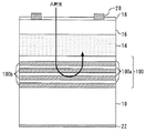
図1は、本発明の実施の形態1に係る光半導体装置を示す断面図である。この光半導体装置は、分布ブラッグ反射層を有するフォトダイオードである。
Embodiment 1 FIG.
FIG. 1 is a sectional view showing an optical semiconductor device according to Embodiment 1 of the present invention. This optical semiconductor device is a photodiode having a distributed Bragg reflection layer.
n型InP基板10(半導体基板)上に、n型DBR層12(第1導電型の分布ブラッグ反射層)、低キャリア濃度のi−InGaAs光吸収層14(光吸収層)、及びp型InP窓層16(第2導電型の半導体層)が順番に形成されている。p型InP窓層16上には、反射防止膜と表面保護膜を兼ねたSiNなどの絶縁膜18とアノード(p型)電極20が形成されている。n型InP基板10の裏面にはカソード(n型)電極22が形成されている。
On an n-type InP substrate 10 (semiconductor substrate), an n-type DBR layer 12 (first conductivity type distributed Bragg reflection layer), a low carrier concentration i-InGaAs light absorption layer 14 (light absorption layer), and a p-type InP Window layers 16 (second conductivity type semiconductor layers) are sequentially formed. On the p-type
n型DBR層12は、屈折率が低いn型InP層12a(第1半導体層)と屈折率が高いn型InGaAs層12b(第2半導体層)を交互に積層したものである。n型InP層12aは、バンドギャップ波長が入射光の波長λより小さく、入射光を吸収しない。一方、n型InGaAs層12bは、バンドギャップ波長が入射光の波長λより大きく、入射光を吸収する。
The n-
また、1層のn型InP層12aの光学層厚(=層厚×屈折率)と1層のn型InGaAs層12bの光学層厚の和は入射光の波長λの半分(=λ/2)である。このため、n型DBR層12は、波長λの入射光に対して効率良く反射層として働く。
The sum of the optical layer thickness (= layer thickness × refractive index) of one n-
また、本実施の形態では、n型InP層12aの光学層厚はn型InGaAs層12bの光学層厚より大きい。例えば、InP層の光学層厚をInGaAs層の光学層厚で割った値が約2.2である。この構成による効果については後に詳細に説明する。
In the present embodiment, the optical layer thickness of the n-
本実施の形態に係る光半導体装置の動作について説明する。アノード電極20の電位がカソード電極22の電位に比べて低くなるように0.5〜3Vの逆バイアスが印加される。入射光は、図の上側から絶縁膜18とp型InP窓層16を通ってi−InGaAs光吸収層14へ入射される。そして、入射光はi−InGaAs光吸収層14で吸収される。
The operation of the optical semiconductor device according to this embodiment will be described. A reverse bias of 0.5 to 3 V is applied so that the potential of the
i−InGaAs光吸収層14の層厚をt、i−InGaAs光吸収層14の入射光に対する吸収係数をαとすると、i−InGaAs光吸収層14に吸収された入射光の割合(=量子効率)は以下の式(1)で表される。
1−exp(−α・t)・・・(1)
If the thickness of the i-InGaAs
1-exp (−α · t) (1)
i−InGaAs光吸収層14で吸収されずに透過した光は、n型DBR層12で反射されて、再びi−InGaAs光吸収層14で吸収される。n型DBR層12における光の反射率をRとすると、n型DBR層12による戻り光を考慮した場合の量子効率は以下の式(2)で表される。
1−exp(−α・t)+R・exp(−α・t)・(1−exp(−α・t))・・・(2)
The light transmitted without being absorbed by the i-InGaAs
1−exp (−α · t) + R · exp (−α · t) · (1−exp (−α · t)) (2)
式(1)と式(2)の差がn型DBR層12による量子効率の増加分である。i−InGaAs光吸収層14の中は、逆バイアスのために空乏層化している。空乏層中は電界がかかっており、電子と正孔は、それぞれカソード電極22とアノード電極20側に流れて電流として取り出される。
The difference between the formula (1) and the formula (2) is an increase in quantum efficiency due to the n-
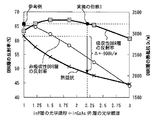
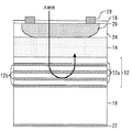
本実施の形態に係る光半導体装置の効果について参考例と比較しながら説明する。図2は、光半導体装置の参考例を示す断面図である。n型DBR層100は、屈折率が異なるn型InP層100aとn型InGaAsP層100bを交互に積層したものである。n型InP層100aとn型InGaAsP層100bの両方とも、バンドギャップ波長が入射光の波長λより小さく、入射光を吸収しない。DBR層以外は本実施の形態に係る光半導体装置と同様である。
The effect of the optical semiconductor device according to the present embodiment will be described in comparison with a reference example. FIG. 2 is a cross-sectional view showing a reference example of the optical semiconductor device. The n-
参考例のn型DBR層100は、n型InP層100aの光学層厚とn型InGaAsP層100bの光学層厚がそれぞれλ/4の場合に、反射率が最大となる。例えば、λが1.55umである場合、InPの屈折率を3.169とするとn型InP層100aの層厚は0.123um、InGaAsPの屈折率を3.437とするとn型InGaAsP層100bの層厚は0.113umである。
The n-
ここで、InPの熱伝導率は約70W/mkで、InGaAsやInGaAsPの熱伝導率(=約5W/mk)と比べると約10倍高い。従って、反射層の熱伝導率を上げる(=熱抵抗を下げる)ためには、InP層の層厚を増やし、InGaAs(P)層の層厚を減らせばよい。しかし、参考例では、n型InGaAsP層100bの層厚を減らすと反射率が低下してしまう。これに対し、本実施の形態では、反射率を低下させることなく、n型InGaAsP層12bの層厚を減らすことができる。この理由について以下に詳細に説明する。
Here, the thermal conductivity of InP is about 70 W / mk, which is about 10 times higher than the thermal conductivity of InGaAs or InGaAsP (= about 5 W / mk). Therefore, in order to increase the thermal conductivity of the reflective layer (= lower the thermal resistance), the thickness of the InP layer may be increased and the thickness of the InGaAs (P) layer may be decreased. However, in the reference example, when the layer thickness of the n-
図3は、DBR層の反射率と熱抵抗を計算した図である。図3の横軸は「InP層の光学層厚÷InGaAs(P)層の光学層厚」である。入射光の波長を1.55um、InGaAsPのバンドギャップ波長を1.4umとし、InGaAs光吸収層からDBR層に光を入射するものとして計算を行った。「吸収性DBR層」はInP層とInGaAs層を13ペア積層したものであり、本実施の形態のDBR層に対応する。一方、「非吸収性DBR層」はInP層とInGaAsP層を13ペア積層したものであり、参考例のDBR層に対応する。 FIG. 3 is a diagram in which the reflectance and thermal resistance of the DBR layer are calculated. The horizontal axis of FIG. 3 is “the optical layer thickness of the InP layer ÷ the optical layer thickness of the InGaAs (P) layer”. The calculation was performed assuming that the wavelength of incident light is 1.55 μm, the band gap wavelength of InGaAsP is 1.4 μm, and light is incident on the DBR layer from the InGaAs light absorption layer. “Absorptive DBR layer” is a stack of 13 pairs of InP layers and InGaAs layers, and corresponds to the DBR layer of this embodiment. On the other hand, the “non-absorbing DBR layer” is a stack of 13 pairs of InP layers and InGaAsP layers, and corresponds to the DBR layer of the reference example.
非吸収性DBR層では、「InP層の光学層厚÷InGaAsP層の光学層厚」が1の場合に反射率が最大になる。一方、吸収性DBR層では、「InP層の光学層厚÷InGaAs層の光学層厚」が1.75付近で反射率が最大になる。従って、吸収性DBR層は、反射率を非吸収性DBR層と同程度に保ちながら、InGaAs層を非吸収性DBR層よりも薄くすることができる。これは、入射光を吸収するInGaAs層を薄くすることで吸収が減り、高い反射率が得られるからである。また、InGaAsPに比べてInGaAsの方がInPに対する屈折率差が大きいからである。 In the non-absorbing DBR layer, when “the optical layer thickness of the InP layer ÷ the optical layer thickness of the InGaAsP layer” is 1, the reflectance is maximized. On the other hand, in the absorptive DBR layer, the reflectance becomes maximum when “the optical layer thickness of the InP layer ÷ the optical layer thickness of the InGaAs layer” is around 1.75. Therefore, the absorptive DBR layer can make the InGaAs layer thinner than the non-absorptive DBR layer, while keeping the reflectance to the same level as the non-absorptive DBR layer. This is because by reducing the thickness of the InGaAs layer that absorbs incident light, absorption is reduced and a high reflectance can be obtained. In addition, InGaAs has a larger refractive index difference than InP compared to InGaAsP.
図3に示すように、参考例では「InP層の光学層厚÷InGaAs層の光学層厚」が1であり、反射率が最大となっている。これに対し、実施の形態1では「InP層の光学層厚÷InGaAs層の光学層厚」が約2.2であるが、参考例と同程度の反射率(=66%)を実現することができる。従って、InGaAs層が薄いため、DBR層の熱抵抗を参考例よりも900k/Wも低減することができる。よって、本実施の形態に係る光半導体装置は、応答の線形性が良く、量子効率が高い。 As shown in FIG. 3, in the reference example, “the optical layer thickness of the InP layer ÷ the optical layer thickness of the InGaAs layer” is 1, and the reflectance is maximum. On the other hand, in the first embodiment, “the optical layer thickness of the InP layer ÷ the optical layer thickness of the InGaAs layer” is about 2.2, but the same reflectance (= 66%) as the reference example is realized. Can do. Therefore, since the InGaAs layer is thin, the thermal resistance of the DBR layer can be reduced by 900 k / W compared to the reference example. Therefore, the optical semiconductor device according to the present embodiment has good response linearity and high quantum efficiency.
ただし、上記の値に限らず、実施の形態1の構成において「InP層の光学層厚÷InGaAs層の光学層厚」を1.2〜3にすれば、DBR層の反射率を参考例と同程度に保ちながら、DBR層の熱抵抗を低減することができる。 However, the present invention is not limited to the above values, and the reflectance of the DBR layer can be set as a reference example by setting the optical layer thickness of the InP layer / the optical layer thickness of the InGaAs layer to 1.2 to 3 in the configuration of the first embodiment. The thermal resistance of the DBR layer can be reduced while maintaining the same level.
なお、n型InP層12aの代わりに、GaAs層、S層、AlInAs層、バンドギャップ波長が入射光の波長より小さいInGaAsP層やAlGaInAs層などを用いてもよい。n型InGaAs層12bの代わりに、バンドギャップ波長が入射光の波長より大きいInGaAsP層やAlGaInAs層などを用いてもよい。
Instead of n-
実施の形態2.
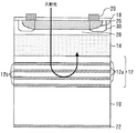
図4は、本発明の実施の形態2に係る光半導体装置を示す断面図である。この光半導体装置は、p型領域を選択拡散で形成したプレーナ型pinフォトダイオードである。
Embodiment 2. FIG.
FIG. 4 is a sectional view showing an optical semiconductor device according to Embodiment 2 of the present invention. This optical semiconductor device is a planar pin photodiode in which a p-type region is formed by selective diffusion.
i−InGaAs光吸収層14上に低キャリア濃度のn型InP層24が形成され、n型InP層24の一部に選択拡散等によりp型InP層26(第2導電型の半導体層)が形成されている。その他の構成は実施の形態1と同様である。これにより実施の形態1と同様の効果を得ることができる。
An n-
実施の形態3.
図5は、本発明の実施の形態3に係る光半導体装置を示す断面図である。この光半導体装置はプレーナ型InPアバランシェフォトダイオードである。
FIG. 5 is a sectional view showing an optical semiconductor device according to
i−InGaAs光吸収層14上にn型InP増倍層28(キャリア増倍層)が形成され、n型InP増倍層28の一部に選択拡散等によりp型InP層26(第2導電型の半導体層)が形成されている。p型InP層26の外周にBeのイオン注入などによりガードリング30が形成されている。n型InP増倍層28は、i−InGaAs光吸収層14で発生した光キャリアをアバランシェ増倍する。その他の構成は実施の形態1と同様である。
An n-type InP multiplication layer 28 (carrier multiplication layer) is formed on the i-InGaAs
アバランシェフォトダイオードは空間電荷効果が特に生じやすく、かつ高い電圧で使用するために発熱量が大きいが、DBR層の熱抵抗を低減することで高光入力時にも安定に動作する。 Avalanche photodiodes are particularly susceptible to space charge effects and generate a large amount of heat because they are used at a high voltage. However, the avalanche photodiode operates stably even at high light input by reducing the thermal resistance of the DBR layer.
実施の形態4.
図6は、本発明の実施の形態4に係る光半導体装置を示す断面図である。この光半導体装置はプレーナ型AlInAsアバランシェフォトダイオードである。
Embodiment 4 FIG.
FIG. 6 is a sectional view showing an optical semiconductor device according to Embodiment 4 of the present invention. This optical semiconductor device is a planar AlInAs avalanche photodiode.
n型DBR層12とi−InGaAs光吸収層14の間に、n型AlInAs増倍層32(キャリア増倍層)と電界緩和層34が形成されている。n型AlInAs増倍層32は、i−InGaAs光吸収層14で発生した光キャリアをアバランシェ増倍する。その他の構成は実施の形態2と同様である。
An n-type AlInAs multiplication layer 32 (carrier multiplication layer) and an electric
発熱源となるn型AlInAs増倍層32の近くに、熱抵抗が低いn型InP層12aが存在するため、効率良く放熱を行うことができる。また、n型DBR層12の屈折率が低い層として、n型InP層12aの代わりに、n型AlInAs増倍層32と同じAlInAs層を用いれば、材料が同じなので結晶成長を安定に行うことができる。
Since the n-
実施の形態5.
図7は、本発明の実施の形態5に係る光半導体装置を示す断面図である。この光半導体装置は実施の形態4と同様にプレーナ型AlInAsアバランシェフォトダイオードである。
Embodiment 5 FIG.
FIG. 7 is a sectional view showing an optical semiconductor device according to Embodiment 5 of the present invention. This optical semiconductor device is a planar type AlInAs avalanche photodiode as in the fourth embodiment.
n型DBR層12のn型InP層12aとn型AlInAs増倍層32の間にキャリア濃度の高いn型AlInAs層36を挿入している。その他の構成は実施の形態4と同様である。これにより、n型AlInAs増倍層32の電界がn型InP層12aにかからないため、n型InP層12aでの正孔の増倍が抑制され、低雑音のアバランシェフォトダイオードを実現することができる。
An n-
実施の形態6.
図8は、本発明の実施の形態6に係る光半導体装置を示す断面図である。この光半導体装置は基板側から光を入射する裏面入射共振型フォトダイオードである。
Embodiment 6 FIG.
FIG. 8 is a sectional view showing an optical semiconductor device according to Embodiment 6 of the present invention. This optical semiconductor device is a back-illuminated resonance type photodiode that receives light from the substrate side.
n型InP基板10の裏面に反射防止膜40が形成されている。そして、n型InP基板10の裏面側から光を入射する。その他の構成は実施の形態2と同様である。
An
n型DBR層12が光の入射側にあるが、屈折率が高いn型InGaAs層12bが薄いので、入射光の損失が少ないという利点がある。その他、実施の形態1,2と同様の効果を得ることができる
Although the n-
実施の形態7.
図9は、本発明の実施の形態7に係る光半導体装置を示す断面図である。この光半導体装置は共振型フォトダイオードである。
Embodiment 7 FIG.
FIG. 9 is a sectional view showing an optical semiconductor device according to Embodiment 7 of the present invention. This optical semiconductor device is a resonant photodiode.
実施の形態1のp型InP窓層16の代わりにp型DBR層38(第2導電型の分布ブラッグ反射層)が形成されている。その他の構成は実施の形態1と同様である。
Instead of the p-type
p型DBR層38は、屈折率が低いp型InP層38a(第1半導体層)と屈折率が高いp型InGaAs層38b(第2半導体層)を交互に積層したものである。p型InP層38aは、バンドギャップ波長が入射光の波長λより小さく、入射光を吸収しない。一方、p型InGaAs層38bは、バンドギャップ波長が入射光の波長λより大きく、入射光を吸収する。
The p-
また、1層のp型InP層38aの光学層厚と1層のp型InGaAs層38bの光学層厚の和は入射光の波長λの半分(=λ/2)である。このため、n型DBR層12は、波長λの入射光に対して効率良く反射層として働く。
The sum of the optical layer thickness of one p-
また、p型InP層38aの光学層厚はp型InGaAs層38bの光学層厚より大きい。具体的には、「InP層の光学層厚÷InGaAs層の光学層厚」は1.2〜3である。このように熱抵抗が大きいp型InGaAs層38bが薄いため、n型DBR層12は放熱性が良い。
The optical layer thickness of the p-
このようにi−InGaAs光吸収層14の上下をDBR層で挟むと、上下のDBR層の間で光が往復することにより高い感度を得ることができるが、熱の逃げ場所がなくなりi−InGaAs光吸収層14に熱が閉じ篭ってしまう。そこで、上記のように放熱の良いDBR層を用いることで、放熱性を改善できる。よって、本実施の形態に係る光半導体装置は、応答の線形性が良く、量子効率が高い。また、屈折率が高いp型InGaAs層38bが薄いので、入射光の損失が少ないという利点もある。
When the upper and lower sides of the i-InGaAs
実施の形態8.
図10は、本発明の実施の形態8に係る光半導体装置を示す断面図である。この光半導体装置は面発光レーザである。
Embodiment 8 FIG.
FIG. 10 is a sectional view showing an optical semiconductor device according to the eighth embodiment of the present invention. This optical semiconductor device is a surface emitting laser.
n型InP基板10(半導体基板)上に、n型DBR層12(第1導電型の分布ブラッグ反射層)、低キャリア濃度のi−InGaAs活性層42(活性層)、及びp型DBR層38(第2導電型の分布ブラッグ反射層)が順番に形成されている。p型DBR層38上には、反射防止膜と表面保護膜を兼ねたSiNなどの絶縁膜18とアノード(p型)電極20が形成されている。n型InP基板10の裏面にはカソード(n型)電極22が形成されている。
On the n-type InP substrate 10 (semiconductor substrate), an n-type DBR layer 12 (first conductivity type distributed Bragg reflection layer), a low carrier concentration i-InGaAs active layer 42 (active layer), and a p-
n型DBR層12は、屈折率が低いn型InP層12a(第1半導体層)と屈折率が高いn型InGaAs層12b(第2半導体層)を交互に積層したものである。p型DBR層38は、屈折率が低いp型InP層38a(第1半導体層)と屈折率が高いp型InGaAs層38b(第2半導体層)を交互に積層したものである。n型InP層12a及びp型InP層38aは、バンドギャップ波長が出射光の波長λより小さく、出射光を吸収しない。一方、n型InGaAs層12b及びp型InGaAs層38bは、バンドギャップ波長が出射光の波長λより大きく、出射光を吸収する。
The n-
また、1層のn型InP層12aの光学層厚と1層のn型InGaAs層12bの光学層厚の和は出射光の波長λの半分であり、1層のp型InP層38aの光学層厚と1層のp型InGaAs層38bの光学層厚の和は出射光の波長λの半分である。このため、n型DBR層12及びp型DBR層38は、波長λの入射光に対して効率良く反射層として働く。
The sum of the optical layer thickness of one n-
また、n型InP層12aの光学層厚はn型InGaAs層12bの光学層厚より大きく、p型InP層38aの光学層厚はp型InGaAs層38bの光学層厚より大きい。具体的には、「InP層の光学層厚÷InGaAs層の光学層厚」は1.2〜3である。このように熱抵抗が大きいp型InGaAs層38bやp型InGaAs層38bが薄いため、n型DBR層12及びp型DBR層38は放熱性が良い。
The optical layer thickness of the n-
このようにi−InGaAs活性層42の上下をDBR層で挟むと、上下のDBR層の間で光が往復してレーザ発振が起こるが、熱の逃げ場所がなくなりi−InGaAs活性層42に熱が閉じ篭ってしまう。そこで、上記のように放熱の良いDBR層を用いることで、放熱性を改善できる。よって、本実施の形態に係る光半導体装置は、応答の線形性が良く、量子効率が高い。また、屈折率が高いp型InGaAs層38bが薄いので、出射光の損失が少ないという利点もある。
When the upper and lower sides of the i-InGaAs
10 n型InP基板(半導体基板)
12 n型DBR層(第1導電型の分布ブラッグ反射層)
12a n型InP層(第1半導体層)
12b n型InGaAs層(第2半導体層)
14 i−InGaAs光吸収層(光吸収層)
16 p型InP窓層(第2導電型の半導体層)
26 p型InP層(第2導電型の半導体層)
28 n型InP増倍層(キャリア増倍層)
32 n型AlInAs増倍層(キャリア増倍層)
38 p型DBR層(第2導電型の分布ブラッグ反射層)
38a p型InP層(第1半導体層)
38b p型InGaAs層(第2半導体層)
42 i−InGaAs活性層(活性層)
10 n-type InP substrate (semiconductor substrate)
12 n-type DBR layer (first conductivity type distributed Bragg reflection layer)
12a n-type InP layer (first semiconductor layer)
12b n-type InGaAs layer (second semiconductor layer)
14 i-InGaAs light absorption layer (light absorption layer)
16 p-type InP window layer (second conductivity type semiconductor layer)
26 p-type InP layer (second conductivity type semiconductor layer)
28 n-type InP multiplication layer (carrier multiplication layer)
32 n-type AlInAs multiplication layer (carrier multiplication layer)
38 p-type DBR layer (second conductivity type distributed Bragg reflection layer)
38a p-type InP layer (first semiconductor layer)
38b p-type InGaAs layer (second semiconductor layer)
42 i-InGaAs active layer (active layer)
Claims (5)
前記第1導電型の分布ブラッグ反射層は、バンドギャップ波長が入射光の波長より小さく第1の屈折率を有する第1半導体層と、バンドギャップ波長が入射光の波長より大きく前記第1の屈折率より高い第2の屈折率を有する第2半導体層とを交互に複数ペア積層したものであり、
1層の前記第1半導体層の光学層厚と1層の前記第2半導体層の光学層厚の和は入射光の波長の半分であり、
前記第1半導体層の光学層厚は、前記第2半導体層の光学層厚より大きく、
前記第1半導体層はInP、前記第2半導体層はInGaAsであり、
前記第1半導体層の光学層厚を前記第2半導体層の光学層厚で割った値が1.2〜3であることを特徴とする光半導体装置。 A first conductivity type distributed Bragg reflection layer, a light absorption layer, and a second conductivity type semiconductor layer are sequentially formed on the semiconductor substrate,
The first conductivity type distributed Bragg reflection layer includes a first semiconductor layer having a band gap wavelength smaller than the wavelength of incident light and a first refractive index, and a band gap wavelength larger than the wavelength of incident light. A plurality of pairs of second semiconductor layers having a second refractive index higher than the refractive index are alternately stacked,
The sum of the optical layer thickness of one layer of the first semiconductor layer and the optical layer thickness of one layer of the second semiconductor layer is half the wavelength of incident light,
The optical layer thickness of the first semiconductor layer is larger than the optical layer thickness of the second semiconductor layer,
The first semiconductor layer is InP, and the second semiconductor layer is InGaAs;
An optical semiconductor device, wherein a value obtained by dividing the optical layer thickness of the first semiconductor layer by the optical layer thickness of the second semiconductor layer is 1.2 to 3.
前記第2導電型の分布ブラッグ反射層は、バンドギャップ波長が入射光の波長より小さく第3の屈折率を有する第3半導体層と、バンドギャップ波長が入射光の波長より大きく前記第3の屈折率より高い第4の屈折率を有する第4半導体層とを交互に複数ペア積層したものであり、
1層の前記第3半導体層の光学層厚と1層の前記第4半導体層の光学層厚の和は入射光の波長の半分であり、
前記第3半導体層の光学層厚は、前記第4半導体層の光学層厚より大きく、
前記第3半導体層の光学層厚を前記第4半導体層の光学層厚で割った値が1.2〜3であることを特徴とする請求項1記載の光半導体装置。 The second conductivity type semiconductor layer is a second conductivity type distributed Bragg reflection layer;
The distributed Bragg reflection layer of the second conductivity type includes a third semiconductor layer having a third refractive index whose band gap wavelength is smaller than the wavelength of incident light, and the third refraction having a band gap wavelength larger than the wavelength of incident light. A plurality of pairs of fourth semiconductor layers having a fourth refractive index higher than the refractive index, and
The sum of the optical layer thickness of one third semiconductor layer and the optical layer thickness of one fourth semiconductor layer is half the wavelength of incident light,
The optical layer thickness of the third semiconductor layer is larger than the optical layer thickness of the fourth semiconductor layer,
2. The optical semiconductor device according to claim 1, wherein a value obtained by dividing the optical layer thickness of the third semiconductor layer by the optical layer thickness of the fourth semiconductor layer is 1.2 to 3.
Priority Applications (3)
| Application Number | Priority Date | Filing Date | Title |
|---|---|---|---|
| JP2008136918A JP5262293B2 (en) | 2008-05-26 | 2008-05-26 | Optical semiconductor device |
| US12/252,621 US7928472B2 (en) | 2008-05-26 | 2008-10-16 | Optical semiconductor device with a distributed Bragg reflector layer |
| CN2009100081690A CN101593784B (en) | 2008-05-26 | 2009-03-09 | Optical semiconductor device |
Applications Claiming Priority (1)
| Application Number | Priority Date | Filing Date | Title |
|---|---|---|---|
| JP2008136918A JP5262293B2 (en) | 2008-05-26 | 2008-05-26 | Optical semiconductor device |
Publications (3)
| Publication Number | Publication Date |
|---|---|
| JP2009283854A JP2009283854A (en) | 2009-12-03 |
| JP2009283854A5 JP2009283854A5 (en) | 2011-03-17 |
| JP5262293B2 true JP5262293B2 (en) | 2013-08-14 |
Family
ID=41341457
Family Applications (1)
| Application Number | Title | Priority Date | Filing Date |
|---|---|---|---|
| JP2008136918A Active JP5262293B2 (en) | 2008-05-26 | 2008-05-26 | Optical semiconductor device |
Country Status (3)
| Country | Link |
|---|---|
| US (1) | US7928472B2 (en) |
| JP (1) | JP5262293B2 (en) |
| CN (1) | CN101593784B (en) |
Families Citing this family (12)
| Publication number | Priority date | Publication date | Assignee | Title |
|---|---|---|---|---|
| JP5444994B2 (en) * | 2009-09-25 | 2014-03-19 | 三菱電機株式会社 | Semiconductor photo detector |
| KR101028314B1 (en) * | 2010-01-29 | 2011-04-12 | 엘지이노텍 주식회사 | Light emitting device and method for fabricating the same |
| JP2011258809A (en) * | 2010-06-10 | 2011-12-22 | Mitsubishi Electric Corp | Semiconductor photodetector |
| JP2012174977A (en) * | 2011-02-23 | 2012-09-10 | Sumitomo Electric Ind Ltd | Light-receiving element and manufacturing method therefor |
| JP6035921B2 (en) * | 2012-07-10 | 2016-11-30 | 富士通株式会社 | Photodetector and manufacturing method thereof |
| JP5918706B2 (en) * | 2013-02-21 | 2016-05-18 | 日本電信電話株式会社 | Long wavelength surface emitting laser |
| US9876127B2 (en) | 2013-11-22 | 2018-01-23 | Taiwan Semiconductor Manufacturing Company, Ltd. | Backside-illuminated photodetector structure and method of making the same |
| US10553742B2 (en) * | 2016-10-28 | 2020-02-04 | Mitsubishi Electric Corporation | Back-surface-incident type light-receiving device and optical module |
| CN109461778A (en) * | 2018-10-31 | 2019-03-12 | 中国电子科技集团公司第四十四研究所 | A kind of structure and production method improving back-illuminated photodiode responsiveness |
| JP7044048B2 (en) * | 2018-12-19 | 2022-03-30 | 日本電信電話株式会社 | Avalanche photodiode and its manufacturing method |
| JP2021114594A (en) * | 2019-08-27 | 2021-08-05 | 株式会社東芝 | Optical semiconductor element |
| CN114792738A (en) * | 2021-01-26 | 2022-07-26 | 朗美通日本株式会社 | Semiconductor light receiving element |
Family Cites Families (14)
| Publication number | Priority date | Publication date | Assignee | Title |
|---|---|---|---|---|
| JPS62282469A (en) * | 1986-05-30 | 1987-12-08 | Nec Corp | Semiconductor photodetector |
| JPS639163A (en) * | 1986-06-30 | 1988-01-14 | Nec Corp | Semiconductor photodetector |
| JPH0821727B2 (en) * | 1988-11-18 | 1996-03-04 | 日本電気株式会社 | Avalanche photodiode |
| US5212703A (en) * | 1992-02-18 | 1993-05-18 | Eastman Kodak Company | Surface emitting lasers with low resistance bragg reflectors |
| JP3544352B2 (en) * | 2000-10-30 | 2004-07-21 | 日本電気株式会社 | Semiconductor light receiving element |
| JP2004327886A (en) * | 2003-04-28 | 2004-11-18 | Nippon Sheet Glass Co Ltd | Semiconductor photo-receiving element |
| JP2005019599A (en) | 2003-06-25 | 2005-01-20 | Seiko Epson Corp | Optical element and its manufacturing method, optical module, and optical transmission device |
| JP4611066B2 (en) * | 2004-04-13 | 2011-01-12 | 三菱電機株式会社 | Avalanche photodiode |
| US7372886B2 (en) | 2004-06-07 | 2008-05-13 | Avago Technologies Fiber Ip Pte Ltd | High thermal conductivity vertical cavity surface emitting laser (VCSEL) |
| CN100557826C (en) * | 2004-10-25 | 2009-11-04 | 三菱电机株式会社 | Avalanche photodide |
| JP2006253548A (en) * | 2005-03-14 | 2006-09-21 | Mitsubishi Electric Corp | Semiconductor photodetector |
| JP4985954B2 (en) | 2006-06-27 | 2012-07-25 | セイコーエプソン株式会社 | Surface emitting semiconductor laser |
| JP4300245B2 (en) * | 2006-08-25 | 2009-07-22 | キヤノン株式会社 | Optical element equipped with multilayer reflector, surface emitting laser |
| JP4985298B2 (en) | 2007-10-10 | 2012-07-25 | 三菱電機株式会社 | Avalanche photodiode |
-
2008
- 2008-05-26 JP JP2008136918A patent/JP5262293B2/en active Active
- 2008-10-16 US US12/252,621 patent/US7928472B2/en active Active
-
2009
- 2009-03-09 CN CN2009100081690A patent/CN101593784B/en active Active
Also Published As
| Publication number | Publication date |
|---|---|
| CN101593784B (en) | 2012-01-11 |
| US20090289316A1 (en) | 2009-11-26 |
| CN101593784A (en) | 2009-12-02 |
| JP2009283854A (en) | 2009-12-03 |
| US7928472B2 (en) | 2011-04-19 |
Similar Documents
| Publication | Publication Date | Title |
|---|---|---|
| JP5262293B2 (en) | Optical semiconductor device | |
| JP5444994B2 (en) | Semiconductor photo detector | |
| US7294868B2 (en) | Super lattice tunnel junctions | |
| JP5303962B2 (en) | Semiconductor photo detector | |
| JP2009290161A (en) | Optical semiconductor device | |
| JP5239568B2 (en) | Semiconductor photo detector | |
| JP2006253548A (en) | Semiconductor photodetector | |
| WO2006046276A1 (en) | Avalanche photodiode | |
| US7197203B2 (en) | Optical element, optical module, and optical transmission device | |
| US20160240718A1 (en) | Double-pass photodiode with embedded reflector | |
| JP2018026478A (en) | Light-emitting element, light-emitting element array, and optical transmission device | |
| JP2013236012A (en) | Avalanche photodiode and method for manufacturing the same | |
| JP6560642B2 (en) | Avalanche photodiode and manufacturing method thereof | |
| JP2011258809A (en) | Semiconductor photodetector | |
| JP4168437B2 (en) | Semiconductor photo detector | |
| JP7280532B2 (en) | Light receiving element | |
| JP2008244368A (en) | Optical semiconductor module and light-receiving element | |
| TWI289220B (en) | Apparatus for and method of frequency conversion | |
| EP1204148A2 (en) | Planar resonant cavity enhanced photodetector | |
| JP2007019313A (en) | Optical element and optical module | |
| JP2015090880A (en) | Surface emitting laser element, laser element array, light source and optical module | |
| JP2000106471A (en) | Surface emitting laser | |
| JP2010045417A (en) | Semiconductor photodetector | |
| JP2009088445A (en) | Optical component | |
| JPS6320398B2 (en) |
Legal Events
| Date | Code | Title | Description |
|---|---|---|---|
| A521 | Request for written amendment filed |
Free format text: JAPANESE INTERMEDIATE CODE: A523 Effective date: 20110127 |
|
| A621 | Written request for application examination |
Free format text: JAPANESE INTERMEDIATE CODE: A621 Effective date: 20110127 |
|
| A977 | Report on retrieval |
Free format text: JAPANESE INTERMEDIATE CODE: A971007 Effective date: 20120411 |
|
| A131 | Notification of reasons for refusal |
Free format text: JAPANESE INTERMEDIATE CODE: A131 Effective date: 20120424 |
|
| A521 | Request for written amendment filed |
Free format text: JAPANESE INTERMEDIATE CODE: A523 Effective date: 20120531 |
|
| A131 | Notification of reasons for refusal |
Free format text: JAPANESE INTERMEDIATE CODE: A131 Effective date: 20130226 |
|
| A521 | Request for written amendment filed |
Free format text: JAPANESE INTERMEDIATE CODE: A523 Effective date: 20130314 |
|
| TRDD | Decision of grant or rejection written | ||
| A01 | Written decision to grant a patent or to grant a registration (utility model) |
Free format text: JAPANESE INTERMEDIATE CODE: A01 Effective date: 20130402 |
|
| A61 | First payment of annual fees (during grant procedure) |
Free format text: JAPANESE INTERMEDIATE CODE: A61 Effective date: 20130415 |
|
| R150 | Certificate of patent or registration of utility model |
Free format text: JAPANESE INTERMEDIATE CODE: R150 Ref document number: 5262293 Country of ref document: JP Free format text: JAPANESE INTERMEDIATE CODE: R150 |
|
| R250 | Receipt of annual fees |
Free format text: JAPANESE INTERMEDIATE CODE: R250 |
|
| R250 | Receipt of annual fees |
Free format text: JAPANESE INTERMEDIATE CODE: R250 |
|
| R250 | Receipt of annual fees |
Free format text: JAPANESE INTERMEDIATE CODE: R250 |
|
| R250 | Receipt of annual fees |
Free format text: JAPANESE INTERMEDIATE CODE: R250 |
|
| R250 | Receipt of annual fees |
Free format text: JAPANESE INTERMEDIATE CODE: R250 |
|
| R250 | Receipt of annual fees |
Free format text: JAPANESE INTERMEDIATE CODE: R250 |
|
| R250 | Receipt of annual fees |
Free format text: JAPANESE INTERMEDIATE CODE: R250 |
|
| R250 | Receipt of annual fees |
Free format text: JAPANESE INTERMEDIATE CODE: R250 |