WO2012108445A1 - プラズマエッチング方法 - Google Patents
プラズマエッチング方法 Download PDFInfo
- Publication number
- WO2012108445A1 WO2012108445A1 PCT/JP2012/052789 JP2012052789W WO2012108445A1 WO 2012108445 A1 WO2012108445 A1 WO 2012108445A1 JP 2012052789 W JP2012052789 W JP 2012052789W WO 2012108445 A1 WO2012108445 A1 WO 2012108445A1
- Authority
- WO
- WIPO (PCT)
- Prior art keywords
- silicon layer
- deposit
- etching
- gas
- recess
- Prior art date
- Legal status (The legal status is an assumption and is not a legal conclusion. Google has not performed a legal analysis and makes no representation as to the accuracy of the status listed.)
- Ceased
Links
Images






Classifications
-
- H—ELECTRICITY
- H10—SEMICONDUCTOR DEVICES; ELECTRIC SOLID-STATE DEVICES NOT OTHERWISE PROVIDED FOR
- H10P—GENERIC PROCESSES OR APPARATUS FOR THE MANUFACTURE OR TREATMENT OF DEVICES COVERED BY CLASS H10
- H10P50/00—Etching of wafers, substrates or parts of devices
- H10P50/20—Dry etching; Plasma etching; Reactive-ion etching
- H10P50/24—Dry etching; Plasma etching; Reactive-ion etching of semiconductor materials
- H10P50/242—Dry etching; Plasma etching; Reactive-ion etching of semiconductor materials of Group IV materials
-
- H—ELECTRICITY
- H10—SEMICONDUCTOR DEVICES; ELECTRIC SOLID-STATE DEVICES NOT OTHERWISE PROVIDED FOR
- H10P—GENERIC PROCESSES OR APPARATUS FOR THE MANUFACTURE OR TREATMENT OF DEVICES COVERED BY CLASS H10
- H10P50/00—Etching of wafers, substrates or parts of devices
- H10P50/69—Etching of wafers, substrates or parts of devices using masks for semiconductor materials
- H10P50/691—Etching of wafers, substrates or parts of devices using masks for semiconductor materials for Group V materials or Group III-V materials
- H10P50/693—Etching of wafers, substrates or parts of devices using masks for semiconductor materials for Group V materials or Group III-V materials characterised by their size, orientation, disposition, behaviour or shape, in horizontal or vertical plane
- H10P50/695—Etching of wafers, substrates or parts of devices using masks for semiconductor materials for Group V materials or Group III-V materials characterised by their size, orientation, disposition, behaviour or shape, in horizontal or vertical plane characterised by the process involved to create the mask, e.g. lift-off masks or sidewalls or to modify the mask
-
- H—ELECTRICITY
- H10—SEMICONDUCTOR DEVICES; ELECTRIC SOLID-STATE DEVICES NOT OTHERWISE PROVIDED FOR
- H10W—GENERIC PACKAGES, INTERCONNECTIONS, CONNECTORS OR OTHER CONSTRUCTIONAL DETAILS OF DEVICES COVERED BY CLASS H10
- H10W20/00—Interconnections in chips, wafers or substrates
- H10W20/01—Manufacture or treatment
- H10W20/021—Manufacture or treatment of interconnections within wafers or substrates
- H10W20/023—Manufacture or treatment of interconnections within wafers or substrates the interconnections being through-semiconductor vias
-
- H—ELECTRICITY
- H10—SEMICONDUCTOR DEVICES; ELECTRIC SOLID-STATE DEVICES NOT OTHERWISE PROVIDED FOR
- H10W—GENERIC PACKAGES, INTERCONNECTIONS, CONNECTORS OR OTHER CONSTRUCTIONAL DETAILS OF DEVICES COVERED BY CLASS H10
- H10W20/00—Interconnections in chips, wafers or substrates
- H10W20/01—Manufacture or treatment
- H10W20/021—Manufacture or treatment of interconnections within wafers or substrates
- H10W20/023—Manufacture or treatment of interconnections within wafers or substrates the interconnections being through-semiconductor vias
- H10W20/0245—Manufacture or treatment of interconnections within wafers or substrates the interconnections being through-semiconductor vias comprising use of blind vias during the manufacture
-
- H—ELECTRICITY
- H01—ELECTRIC ELEMENTS
- H01J—ELECTRIC DISCHARGE TUBES OR DISCHARGE LAMPS
- H01J2237/00—Discharge tubes exposing object to beam, e.g. for analysis treatment, etching, imaging
- H01J2237/32—Processing objects by plasma generation
- H01J2237/33—Processing objects by plasma generation characterised by the type of processing
- H01J2237/334—Etching
Definitions
- the present invention provides a plasma etching method in which a plasma of a processing gas is supplied to a substrate on which a resist mask, an intermediate film containing silicon and nitrogen, and a silicon layer are stacked from above, and the silicon film is etched to form a recess. Regarding the method.
- wafers substrates such as semiconductor wafers (hereinafter referred to as “wafers”) on which integrated circuits are mounted are three-dimensionally integrated, and wiring metal embedded in each wafer. Therefore, a structure for electrically connecting adjacent wafers to each other has been studied.
- a recess such as a hole for embedding the wiring metal in the wafer is formed in each wafer by plasma etching.
- a wafer includes, for example, a single crystal silicon (Si) layer in which the recess is formed, and a resist mask that is laminated above the silicon layer and patterned to correspond to the pattern of the recess. It has.
- a CMP (Chemical Mechanical Policing) process performed to remove excess wiring metal after embedding wiring metal in the recess.
- an intermediate film containing silicon such as a silicon nitride (SiN) film is interposed. Therefore, after etching the intermediate film to expose the silicon layer, the silicon layer is etched.
- the recess may be formed to a depth of 100 ⁇ m with respect to an opening diameter of about 10 ⁇ m, for example. Therefore, for example, while the silicon layer is etched by the plasma of the processing gas containing sulfur fluoride (SF 6 ) gas or oxygen (O 2 ) gas, the sidewall of the silicon nitride film is exposed to the plasma. become. For this reason, the silicon nitride film may be side-etched from the side (recess side), and a gap may be formed between the resist mask and the silicon film around the recess. When this gap is formed, the desired metal characteristics cannot be obtained, for example, the wiring metal enters the gap in a subsequent process and the leakage current increases.
- the processing gas containing sulfur fluoride (SF 6 ) gas or oxygen (O 2 ) gas oxygen
- the silicon nitride film may be side-etched from the side (recess side), and a gap may be formed between the resist mask and the silicon film around the recess.
- Patent Document 1 describes a technique for suppressing undercut generation by forming a protective film on the side wall of a photoresist film using, for example, plasma of C 4 F 8 gas.
- JP2009-206410 (paragraph 0047 and the like)
- the present invention has been made under such circumstances.
- the object of the present invention is to provide a resist mask, an intermediate film containing silicon and nitrogen, and a substrate on which a silicon layer is laminated in this order from the upper side.
- An object of the present invention is to provide a plasma etching method capable of suppressing the occurrence of side etching of the intermediate film when a recess is formed in a silicon layer by performing a plasma etching process through a mask pattern.
- an intermediate film containing silicon and nitrogen located under a resist mask formed on the surface of a substrate is etched with a processing gas to expose a silicon layer located under the intermediate film.
- the reaction product when the processing gas containing a compound of sulfur and fluorine is supplied to the silicon layer and the portion corresponding to the opening is etched to form the recess, the reaction product is an intermediate film. Therefore, the side etching of the intermediate film can be suppressed.
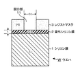
- the wafer W includes, for example, a silicon nitride (SiN) film 2 containing silicon and nitrogen (N) 2 and a resist mask 3 in this order from the lower side on a single crystal silicon (Si) layer 1.
- SiN silicon nitride
- the silicon nitride (SiN) film 2 is an example of an intermediate film having a thickness dimension t of 100 ⁇ m, for example.
- the resist mask 3 is made of resin or the like.
- a cylindrical opening 11 having an opening diameter (diameter dimension) D1 of, for example, 11.2 ⁇ m is patterned at a plurality of locations. As will be described later, at a position corresponding to each opening 11.
- a recess 12 (see FIG. 4) such as a hole having a depth of, for example, 100 ⁇ m is formed in the silicon nitride film 2 and the silicon layer 1 on the lower layer side by plasma of the processing gas.
- the recess 12 when the recess 12 is formed in the silicon layer 1, the silicon nitride film 2 is not side-etched from the side (the recess 12 side) or the side of the silicon nitride film 2 is formed.
- a protective film (attachment 13) is formed on the side wall of the silicon nitride film 2 so that etching is suppressed.
- FIG. 1 an area near one opening 11 on the wafer W is shown enlarged.
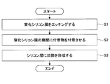
- the plasma etching step is a first step of etching the silicon nitride film 2 (step S1), and the silicon layer 1 is etched slightly (for example, about 1 ⁇ m) on the sidewall of the silicon nitride film 2.
- the term “concave portion 12” is also used for a region formed by etching the silicon layer 1 in the step of forming the protective film.
- Step S1 Etching process of silicon nitride film
- the processing atmosphere in a processing container 50 described later
- the processing gas plasma includes SF 6 (sulfur fluoride) gas and O 2 (oxygen) gas. Is supplied to the wafer W.
- the silicon nitride film 2 is etched through the resist mask 3 to expose the lower silicon layer 1.
- the resist mask 3 is also etched by the plasma, since the etching selectivity of the silicon nitride film 2 with respect to the resist mask 3 is considerably large, the illustration is omitted in FIG. The same applies to the subsequent FIGS.
- Step S2 Protection Film Formation Process
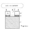
- the degree of vacuum of the processing atmosphere is set in the range of 6.67 Pa (50 mTorr) to 13.33 Pa (100 mTorr) and chlorine is used as the processing gas (etching gas).
- (Cl 2 ) gas is supplied to the processing atmosphere at a flow rate of 200 sccm or more.
- the degree of vacuum of the processing atmosphere is set to 6.67 Pa (50 mTorr), and chlorine (Cl 2 ) gas is supplied to the processing atmosphere as a processing gas (etching gas) at a flow rate of 400 sccm.
- silicon chloride SiCl 4
- SiCl 4 silicon chloride
- the resist mask 3 the silicon nitride film 2
- the silicon It adheres (deposits) as a deposit 13 on the side wall of the recess 12 in the layer 1.
- the deposit 13 is less likely to be etched than the silicon layer 1 and the silicon nitride film 2. Therefore, the deposit 13 functions as a protective film for the silicon nitride film 2 in the etching process of the silicon layer 1 performed after the depositing process of the deposit 13.
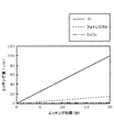
- the vertical axis represents the etching amount (film thickness) when various films (Si film, photoresist film, SiN film, SiO 2 film, and SiCl 4 film) are etched, and the horizontal axis represents The etching time for etching each film is shown.
- 6 is an enlarged graph of the vicinity of the lower side (zero) of the vertical axis in FIG.
- the opening diameter D1 of the recess 12 formed in the silicon layer 1 gradually narrows as the depositing process of the deposit 13 proceeds.
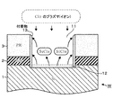
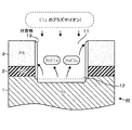
- the recess 12 is formed to have approximately the same dimensions as the opening 11 of the resist mask 3, for example, as shown in FIG. If the deposit 13 adheres to the side wall of the recess 12 by this etching, the deposit 13 becomes a barrier against chlorine ions (plasma) drawn into the wafer W side. Therefore, as shown in FIG. 8, the silicon layer 1 is etched by the chlorine ions using the deposit 13 attached to the inner wall surface of the recess 12 of the silicon layer 1 in the circumferential direction as a mask. 7 and 8 schematically show the vicinity of the opening 11 of the resist mask 3 in an enlarged manner, and the depth dimension of the opening 11 is exaggerated and drawn greatly.
- the deposit 13 again adheres to the newly exposed inner wall surface of the recess 12, and the silicon layer 1 is further etched using the deposit 13 as a mask.
- the opening diameter D1 gradually decreases. Therefore, when the opening “D2” (see FIG. 4) is attached to the opening diameter at the lower end of the recess 12 formed by the attaching step of the attached matter 13, the upper end position of the silicon layer 1 is shown in FIG.
- the tapered surface 14 whose opening diameter is gradually reduced from D1 to D2 from the upper side to the lower side is formed in the circumferential direction.
- the taper of the silicon layer 1 from the resist mask 3 is continued.
- the adhering matter 13 adheres and accumulates on the inner peripheral surfaces of the opening 11 and the recess 12 over the surface 14.
- the depth dimension h1 of the silicon layer 1 etched by the plasma of chlorine gas is, for example, 1 ⁇ m.
- the aforementioned opening diameter D2 is, for example, 10 ⁇ m. Since the silicon layer 1 is etched with high anisotropy by chlorine ions, side etching from the side of the silicon layer 1 is suppressed.
- the width dimension u of the deposit 13 is set from the following viewpoint. As shown in FIGS. 5 and 6 described above, the deposit 13 containing silicon and chlorine is less etched than the silicon nitride film 2 and the silicon layer 1, but is slightly etched. Therefore, if the deposit 13 attached to the sidewall of the silicon nitride film 2 is removed (etched) in the course of the subsequent etching process of the silicon layer 1, the silicon nitride film 2 can be effectively protected. There is a risk of not being able to.
- the deposit 13 remains on the side wall of the silicon nitride film 2 after the etching process of the silicon layer 1 is finished, it becomes difficult to bury the wiring metal in the recess 12 in the subsequent process, or There is also a risk of increasing the electrical resistance of the wiring metal. Therefore, in one embodiment of the present invention, when the etching process of the silicon layer 1 is completed, in this example, when the depth dimension h2 of the recess 12 is about 100 ⁇ m, the side wall attachment of the silicon nitride film 2 is performed. A process of setting the width u of the deposit 13 or removing the deposit 13 is added so that the deposit 13 is removed by etching or the deposit 13 is hardly left.
- the silicon layer 1 and the deposit 13 are etched using a processing gas (etching gas) in the etching process of the silicon layer 1, and these silicon layers are etched.
- the etching amount (film thickness) per unit time in each of 1 and the deposit 13 is measured in advance.
- the time required for etching the depth dimension h2 (100 ⁇ m in this example) of the recess 12 formed in the silicon layer 1 is calculated, it is 20 minutes in this example. Therefore, the deposit 13 is preferably left for 20 minutes during the etching process of the silicon layer 1 (removed after 20 minutes).
- the thickness of the deposit 13 etched in 20 minutes is about 0.6 ⁇ m, and therefore the width u of the deposit 13 formed on the sidewall of the silicon nitride film 2 is 0.6 ⁇ m.
- the width u of the deposit 13 may vary from the upper end side to the lower end side of the silicon nitride film 2. Specifically, the width u of the deposit 13 may be thicker on the upper end side than on the lower end side. Accordingly, when it is desired to suppress the side etching of the silicon nitride film 2 as much as possible with respect to the width dimension u of the deposit 13 to be adhered to the sidewall of the silicon nitride film 2, the deposit 13 from the upper end side to the lower end side of the silicon nitride film 2 is prevented.
- the minimum value of the width dimension u is set to be 0.6 ⁇ m or 0.6 ⁇ m or more as described above.
- the maximum value of the width dimension u of the deposit 13 from the upper end side to the lower end side of the silicon nitride film 2 is 0 as described above. It is set to be 6 ⁇ m or 0.6 ⁇ m or less. At this time, as described above, instead of setting the width dimension u of the deposit 13 as described above, or the width dimension u is set as described above and the deposit 13 is removed. May be.
- Step S3 Etching Process of Silicon Layer 1
- SF 6 gas, SiF 4 (fluorinated) Plasma radical of a processing gas including silicon) gas, O 2 gas, and HBr (hydrogen bromide) gas is supplied to the wafer W.
- SF 6 gas, SiF 4 (fluorinated) Plasma radical of a processing gas including silicon) gas, O 2 gas, and HBr (hydrogen bromide) gas is supplied to the wafer W.
- SF 6 gas, SiF 4 (fluorinated) Plasma radical of a processing gas including silicon) gas, O 2 gas, and HBr (hydrogen bromide) gas is supplied to the wafer W.
- HBr hydrogen bromide
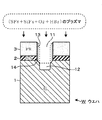
- the lower end side (inner peripheral side) of the tapered surface 14 described above is exposed. Therefore, since the lower end side of the tapered surface 14 is also etched downward, the tapered angle of the tapered surface 14 becomes steeper as the silicon layer 1 is etched. As the silicon layer 1 is etched, it is considered that fluorine derived from SF 6 gas or radicals (active species) containing fluorine and sulfur contribute particularly in the plasma.
- the etching process of the silicon layer 1 is performed until the depth dimension h2 of the recess 12 reaches, for example, about 100 ⁇ m, the resist mask 3, the silicon nitride film 2, and the silicon layer 1 adhere to the upper end portions as shown in FIG.
- the attached deposit 13 is removed or almost disappeared.
- the tapered surface 14 described above is gradually exposed to plasma from the lower end side (inner peripheral side) toward the upper end side (outer peripheral side) as the etching of the silicon layer 1 proceeds, so the taper angle Becomes steeper (approaching the vertical direction), and for example, a tapered surface 14 is formed in the vertical direction of the recess 12.
- the resist mask 3 is ashed with plasma of a processing gas containing O 2 gas, and then the surface of the wafer W is cleaned.
- a wiring metal 15 such as copper (Cu) is embedded in the recess 12 by CVD (Chemical Mechanical Deposition), electrolytic plating, electroless plating, or the like.
- CVD Chemical Mechanical Deposition
- electrolytic plating electroless plating
- excess wiring metal 15 formed on the surface of the wafer W is removed by CMP (Chemical Mechanical Policing) processing.
- the silicon nitride film 2 acts as a stopper film, and the end point of the CMP process is detected at the upper end position of the silicon nitride film 2.
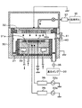
- This apparatus includes a mounting table 31 that forms a lower electrode for mounting a wafer W, and a lower two-frequency unit that includes a gas shower head 32 provided on the upper side of the processing container 50 so as to face the mounting table 31. It is comprised as an etching apparatus.
- the high-frequency power source 33a for plasma generation and the high-frequency power source 33b for bias in FIG. 12 are connected to the mounting table 31 via a matching unit 34a and a matching unit 34b, respectively.
- the high frequency power supply 33a outputs a high frequency with a frequency of 40 MHz, for example, and the high frequency power supply 33b outputs a high frequency with a frequency of 2 MHz, for example.
- the gas shower head 32 has a plurality of gas supply holes 32 a formed on the lower surface of the gas shower head 32.
- the processing gas is output from the processing gas supply source 35 and is supplied above the wafer W held by the electrostatic chuck 31a on the mounting table 31 through the gas supply hole 32a.
- the vacuum pump 36 evacuates the atmosphere in the processing container 50 from the floor surface side of the processing container 50.
- a flow rate adjusting unit 37 including a valve or the like is connected to the processing gas supply source 35.
- a butterfly valve 38 is connected to the vacuum pump 36.
- a temperature control flow path 39 is provided on the mounting table 31.
- the wafer W is loaded or unloaded from the transfer port 40 of the wafer W by opening and closing the gate valve 41.
- the mounting table is connected via the transfer port 40 by the cooperative action of a transfer arm outside the apparatus and a lifting pin (not shown) provided on the lower side of the mounting table 31.
- a wafer W is placed on 31.
- the inside of the processing container 50 is evacuated to adjust the atmosphere in the processing container 50 to the processing pressure, and the processing gas is supplied into the processing container 50.
- 1500 W of power is supplied from the high-frequency power source 33a for plasma generation and the high-frequency power source 33b for bias to the mounting table 31 to turn the processing gas into plasma and draw the plasma to the wafer W side.
- the silicon nitride film 2 and the silicon layer 1 described above are etched.
- the silicon layer 1 is slightly etched using plasma (ions) of a processing gas containing chlorine.
- a deposit 13 containing chlorine and silicon is adhered to the side wall of the silicon film 2.
- the deposit 13 is a substance that is harder to be etched than the silicon layer 1, and the chlorine ions are plasma that performs anisotropic etching. Therefore, even when the recess 12 having a depth of, for example, 100 ⁇ m is formed in the silicon layer 1, side etching can be suppressed for the silicon nitride film 2 that is easily etched by fluorine radicals.
- the width dimension of the upper end position of the wiring metal 15 embedded in the recess 12 can be formed as designed, and for example, a short circuit between the wiring metals 15 and 15 adjacent to each other can be prevented. Therefore, deterioration of characteristics such as an increase in leakage current can be suppressed.
- the side etching of the silicon nitride film 2 is suppressed, the occurrence of undercut (the opening diameter D1 of the recess 12 widens from the upper side toward the lower side) is suppressed with respect to the shape of the recess 12, and the upper side Since etching can be performed so that the opening diameter D2 on the lower side of the opening diameter D1 becomes a narrow taper shape, the wiring metal 15 can be easily embedded in the recess 12.
- the lower end position of the recess 12 is equal to the width dimension u of the deposit 13 attached to the sidewall of the recess 12 (specifically, the width dimension u ⁇ 2). Since it is larger than the opening diameter D2, the opening diameter D2 can be formed as designed.
- the width u of the deposit 13 is set so that the deposit 13 is removed by etching when the recess 12 is formed in the silicon layer 1 or the deposit 13 is hardly left by etching. . Therefore, for example, adverse effects on the wiring metal 15 such as blocking of the recess 12 and an increase in electrical resistance of the wiring metal 15 can be suppressed.
- the deposit 13 can be quickly formed by setting the processing conditions (processing pressure and flow rate of the processing gas) as described above. Further, by setting the processing conditions in this way, the height dimension k of the deposit 13 can be formed large as shown in the examples described later, and therefore, the silicon layer 1 is attracted to the wafer W from above in the etching process of the silicon layer 1.
- the deposit 13 can be highly resistant to the generated plasma.
- the silicon nitride film 2 has been described as an example in the above-described example, but instead of the silicon nitride film 2, a silicon layer is used.
- a compound species that is etched by fluorine radicals in the plasma used for the etching process 1 may be used, such as a SiCN film.
- a treatment gas containing chlorine used for attaching the deposit 13 to the silicon-containing film (silicon nitride film 2) for example, Ar (argon) gas, He ( Helium) gas, O 2 (oxygen) gas, or the like may be used.
- the recess 12 is formed to have a tapered shape, but may be formed to be vertical.
- the step of depositing the deposit 13 on the sidewall of the silicon nitride film 2 is performed by setting the processing pressure to 3E ⁇ 6 Pa to 7E ⁇ 4 Pa (3 ⁇ 10 ⁇ 6 Pa to 7 ⁇ 10 ⁇ 4 Pa).
- the supply flow rate of chlorine gas may be set to 50 to 1000 sccm.
- a lower 1 frequency apparatus or an upper and lower 2 frequency plasma etching apparatus may be used instead of the apparatus of FIG.
- Plasma etching is performed on a 300 mm (12 inch) size wafer W obtained by etching the silicon nitride film 2 so as to be in the state shown in FIG. went. Processing conditions other than the processing pressure are common conditions in each example, and the flow rate of chlorine gas was set to 100 sccm.
- the gas flow rate is preferably 800 sccm or more, for example.
- the deposit 13 is adhered by changing the amount of power supplied to the wafer W from the high frequency power source 33a for generating plasma and the high frequency power source 33b for biasing. It was. And about this deposit
- FIG. 16 by setting the high-frequency power supplied from each of the high-frequency power sources 33a and 33b to 1000 W or more, a good deposit 13 (width dimension u is 0.6 ⁇ m or more) is generated. I understood.
- the high-frequency power of the high-frequency power sources 33a and 33b is 1000 W or more, the dimensions of the deposit 13 are approximately the same.
- the power amount of one of the high-frequency power sources 33a and 33b was set to 1000 W or 1500 W, the other power value was set to 50 W.
- the intermediate film containing silicon and nitrogen located under the resist mask formed on the surface of the substrate is etched with the processing gas, A first step of exposing a silicon layer located below the intermediate film; and then a second step of supplying chlorine gas to the substrate and depositing a reaction product on the resist mask and side walls of the opening of the intermediate film. And a third step of forming a recess by etching a portion corresponding to the opening in the silicon layer using a processing gas containing a compound of sulfur and fluorine.
- the second step may be performed in a pressure atmosphere of 3E ⁇ 6 Pa to 7E ⁇ 4 Pa (3 ⁇ 10 ⁇ 6 Pa to 7 ⁇ 10 ⁇ 4 Pa).
- the substrate is a 12-inch wafer
- chlorine gas is supplied from a gas shower head in which a large number of gas supply holes are formed on the opposing surface facing the substrate, and the supply flow rate of chlorine gas. May be set to 50 sccm to 1000 sccm.
- the film thickness is adjusted so that the reaction product is removed by the processing gas containing the compound of sulfur and fluorine when the recess is formed in the silicon layer in the third step. Then, it may be a step of attaching the reaction product.
Landscapes
- Drying Of Semiconductors (AREA)
- Physics & Mathematics (AREA)
- Engineering & Computer Science (AREA)
- Plasma & Fusion (AREA)
- Internal Circuitry In Semiconductor Integrated Circuit Devices (AREA)
Abstract
Description
本発明の一実施形態に係るプラズマエッチング方法の実施の形態の一例について、図1~図11を参照して説明する。先ず、このプラズマエッチング方法が適用される例えば12インチサイズのウエハWの構成の一例について説明する。このウエハWは、図1に示すように、例えば単結晶シリコン(Si)層1上に、シリコンと窒素(N)とを含む窒化シリコン(SiN)膜2及びレジストマスク3が下側からこの順番で積層されている。窒化シリコン(SiN)膜2は、例えば厚さ寸法tが100μmの中間膜の一例である。また、レジストマスク3は、樹脂などからなる。このレジストマスク3には、開口径(直径寸法)D1が例えば11.2μmの円筒状の開口部11が複数箇所にパターニングされており、後述するように、各々の開口部11に対応する位置において、下層側の窒化シリコン膜2及びシリコン層1に対して、処理ガスのプラズマにより例えば100μmもの深さを持つホールなどの凹部12(図4参照)が形成される。そして、本発明の一実施形態では、シリコン層1に対して凹部12を形成する時に、窒化シリコン膜2が側方側(凹部12側)からサイドエッチングされないように、あるいは窒化シリコン膜2のサイドエッチングが抑えられるように、当該窒化シリコン膜2の側壁に保護膜(付着物13)を形成している。尚、図1ではウエハW上における一つの開口部11付近の領域を拡大して示している。
先ず、窒化シリコン膜2に対してエッチング処理を行う。具体的には、ウエハWの置かれる処理雰囲気(後述の処理容器50内)を真空雰囲気に設定すると共に、SF6(フッ化硫黄)ガスとO2(酸素)ガスとを含む処理ガスのプラズマをウエハWに供給する。このプラズマによって、図3に示すように、レジストマスク3を介して窒化シリコン膜2がエッチングされて下層側のシリコン層1が露出する。尚、前記プラズマによってレジストマスク3についてもエッチングされているが、レジストマスク3に対する窒化シリコン膜2のエッチング選択比がかなり大きいため、図3では図示を省略している。以降の図4~図10についても同様である。
次いで、窒化シリコン膜2の側壁に保護膜を形成する。具体的には、前記処理ガスを排気した後、処理雰囲気の真空度を6.67Pa(50mTorr)~13.33Pa(100mTorr)の範囲のいずれかに設定すると共に、処理ガス(エッチングガス)として塩素(Cl2)ガスを200sccm以上の流量で前記処理雰囲気に供給する。本実施形態では、処理雰囲気の真空度を6.67Pa(50mTorr)に設定すると共に、処理ガス(エッチングガス)として塩素(Cl2)ガスを400sccmの流量で前記処理雰囲気に供給する。そして、この処理ガスにプラズマ発生用の高周波電力を印加すると共に、ウエハWに対してバイアス用の高周波電力を印加すると、処理ガスは、図4に示すように、プラズマ化(イオン化)されてウエハWに向かって引き込まれていく。尚、後述の平行平板型プラズマ装置を用いる場合、平行平板電極間にプラズマ発生用の高周波電力が印加され、下部電極にバイアス用の高周波電力が印加されることになる。この塩素イオンがシリコン層1に接触すると、当該シリコン層1は開口部11に対応するように極めて僅かにエッチングされて凹部12が形成されていく。
次に、シリコン層1のエッチング工程について説明する。始めに、ウエハWの置かれる処理雰囲気を排気して既述の塩素ガスを除去した後、真空雰囲気に設定された処理雰囲気において、図9に示すように、SF6ガス、SiF4(フッ化シリコン)ガス、O2ガス及びHBr(臭化水素)ガスを含む処理ガスのプラズマ(ラジカル)をウエハWに供給する。このプラズマにより、シリコン層1が下方側に向かってエッチングされると共に、レジストマスク3、窒化シリコン膜2及び凹部12の側壁に付着した既述の付着物13についても例えば側方側から僅かにエッチングされていく。この時、付着物13が側方側からエッチングされるにつれて、既述のテーパー面14の下端側(内周側)が露出する。そのため、テーパー面14の下端側についても下方に向かってエッチングされるので、当該テーパー面14は、シリコン層1のエッチング処理が進むにつれて、いわばテーパー角度が急峻になっていく。尚、シリコン層1がエッチングされていくにあたり、プラズマ中において、SF6ガス由来のフッ素、またはフッ素とイオウとを含むラジカル(活性種)が特に寄与していると考えられる。
シリコン層1をエッチングした後、例えばレジストマスク3を、O2ガスを含む処理ガスのプラズマによってアッシングし、次いでウエハWの表面の洗浄を行う。続いて、CVD(Chemical Mechanical Deposition)法や電解メッキあるいは無電解メッキなどにより、凹部12内に例えば銅(Cu)などの配線金属15を埋め込む。その後、図11に示すように、CMP(Chemical Mechanical Policing)加工により、ウエハWの表面に形成された余剰な配線金属15を除去する。この時、窒化シリコン膜2がストッパ膜として作用して、当該窒化シリコン膜2の上端位置においてCMP加工の終点検出が行われる。
続いて、以上のプラズマエッチング方法を実施するためのプラズマエッチング装置の一例について、図12を参照して簡単に説明する。この装置は、ウエハWを載置するための下部電極をなす載置台31と、この載置台31に対向するように処理容器50の上方側に設けられたガスシャワーヘッド32を備えた下部2周波のエッチング装置として構成されている。図12中のプラズマ発生用の高周波電源33a及びバイアス用の高周波電源33bは、各々整合器34a及び整合器34bを介して載置台31に接続される。高周波電源33aは、例えば周波数が40MHzの高周波を出力し、高周波電源33bは、例えば周波数が2MHzの高周波を出力する。
既述の図3の状態となるように窒化シリコン膜2をエッチングした300mm(12インチ)サイズのウエハWに対して、塩素ガスを用いて、以下のように処理圧力を種々変えてプラズマエッチングを行った。処理圧力以外の処理条件は、各例において共通の条件であり、塩素ガスの流量については100sccmに設定した。
実施例:6.67Pa(50mTorr)、13.3Pa(100mTorr)
比較例:2.67Pa(20mTorr)
その結果、図13に示すように、処理圧力が高くなる(真空度が低くなる)程、付着物13の高さ寸法kが高くなり、6.67Pa(50mTorr)以上の処理圧力では付着物13の上端部がレジストマスク3の表面付近にまで到達していた。従って、既述のようにシリコン層1のエッチング時において付着物13の良好なエッチング耐性を得るためには、処理圧力は6.67Pa(50mTorr)以上であることが好ましいことが分かった。尚、図13の下側には、上側に示したSEM(scanning electron microscope)写真を読み取って付着物13と窒化シリコン膜2との境界を示した図を描画している。
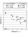
続いて、付着物13を生成させる工程において、塩素ガスの流量を以下の表に示すように種々変えて実験を行った。そして、ウエハWの中央(センター)と端部(エッジ)とにおいて、付着物13の幅寸法u及び高さ寸法kを各々測定した。この実験において、処理圧力を各々6.67Pa(50mTorr)に設定すると共に、2分間に亘って各々エッチング処理を行った。尚、付着物13の幅寸法u及び高さ寸法kについては、図14に示すように、夫々窒化シリコン膜2の上端位置における寸法及び当該付着物13の上端位置から窒化シリコン膜2の上端位置までの間における寸法である。

その結果、上記表及び図15に示すように、いずれの条件においても良好な付着物13が得られた。付着物13の幅寸法uについては、処理ガスの流量を増やす程厚くなっていることが分かった。そのため、付着物13を速やかに得るためには、ガス流量が例えば800sccm以上であることが好ましい。尚、実験結果などの説明については省略するが、処理ガスの流量が200sccm以上であれば、各例と同様に付着物13が得られる。
また、既述の図12のプラズマエッチング装置を用いて、プラズマ発生用の高周波電源33a及びバイアス用の高周波電源33bからウエハWに対して各々供給する電力量を種々変えて付着物13を付着させた。そして、この付着物13について、ウエハWの中央部側及び端部側において、幅寸法u及び高さ寸法kを夫々測定した。その結果、図16に示すように、各高周波電源33a、33bから供給する高周波電力を1000W以上に設定することにより、良好な(幅寸法uが0.6μm以上の)付着物13が生成することが分かった。また、これら高周波電源33a、33bの高周波電力が1000W以上では、付着物13の各寸法はほぼ同程度となっていた。尚、この実験において、各高周波電源33a、33bの一方の電力量を1000Wあるいは1500Wに設定するにあたり、他方の電力値については50Wに設定した。
以上に説明したように、本発明の一実施形態に係るプラズマエッチング方法は、基板の表面に形成されたレジストマスクの下方に位置する、シリコン及び窒素を含む中間膜を処理ガスによりエッチングして、前記中間膜の下方に位置するシリコン層を露出させる第1の工程と、次いで塩素ガスを基板に供給し、前記レジストマスク及び中間膜の開口部の側壁に反応生成物を付着させる第2の工程と、その後、イオウとフッ素との化合物を含む処理ガスを用いて前記シリコン層における前記開口部に対応する部位をエッチングして凹部を形成する第3の工程と、を含む。
1 シリコン層
2 窒化シリコン膜
3 レジストマスク
11 開口部
12 凹部
13 付着物
14 テーパー面
15 配線金属
Claims (4)
- 基板の表面に形成されたレジストマスクの下方に位置する、シリコン及び窒素を含む中間膜を処理ガスによりエッチングして、前記中間膜の下方に位置するシリコン層を露出させる第1の工程と、
次いで塩素ガスを基板に供給し、前記レジストマスク及び中間膜の開口部の側壁に反応生成物を付着させる第2の工程と、
その後、イオウとフッ素との化合物を含む処理ガスを用いて前記シリコン層における前記開口部に対応する部位をエッチングして凹部を形成する第3の工程と、を含むことを特徴とするプラズマエッチング方法。 - 前記第2の工程は、3×10⁻⁶Pa~7×10⁻⁴Paの圧力雰囲気下で行うことを特徴とする請求項1に記載のプラズマエッチング方法。
- 前記基板は12インチウエハであり、
前記第2の工程は、基板に対向する対向面に多数のガス供給孔が形成されたガスシャワーヘッドから塩素ガスを供給すると共に、塩素ガスの供給流量を50sccm~1000sccmに設定して行うことを特徴とする請求項1に記載のプラズマエッチング方法。 - 前記第2の工程は、前記第3の工程において前記シリコン層に凹部を形成した時に、前記イオウとフッ素との化合物を含む処理ガスによって反応生成物が除去されるように膜厚を調整して反応生成物を付着させる工程であることを特徴とする請求項1に記載のプラズマエッチング方法。
Priority Applications (2)
| Application Number | Priority Date | Filing Date | Title |
|---|---|---|---|
| US13/983,826 US8975191B2 (en) | 2011-02-08 | 2012-02-07 | Plasma etching method |
| KR1020137021021A KR101894613B1 (ko) | 2011-02-08 | 2012-02-07 | 플라즈마 에칭 방법 |
Applications Claiming Priority (2)
| Application Number | Priority Date | Filing Date | Title |
|---|---|---|---|
| JP2011-025083 | 2011-02-08 | ||
| JP2011025083A JP5712653B2 (ja) | 2011-02-08 | 2011-02-08 | プラズマエッチング方法 |
Publications (1)
| Publication Number | Publication Date |
|---|---|
| WO2012108445A1 true WO2012108445A1 (ja) | 2012-08-16 |
Family
ID=46638658
Family Applications (1)
| Application Number | Title | Priority Date | Filing Date |
|---|---|---|---|
| PCT/JP2012/052789 Ceased WO2012108445A1 (ja) | 2011-02-08 | 2012-02-07 | プラズマエッチング方法 |
Country Status (5)
| Country | Link |
|---|---|
| US (1) | US8975191B2 (ja) |
| JP (1) | JP5712653B2 (ja) |
| KR (1) | KR101894613B1 (ja) |
| TW (1) | TWI475612B (ja) |
| WO (1) | WO2012108445A1 (ja) |
Families Citing this family (11)
| Publication number | Priority date | Publication date | Assignee | Title |
|---|---|---|---|---|
| CN103972055B (zh) * | 2013-01-31 | 2016-09-07 | 中微半导体设备(上海)有限公司 | 光刻胶去除方法 |
| JP5889368B2 (ja) * | 2013-09-05 | 2016-03-22 | Sppテクノロジーズ株式会社 | プラズマエッチング方法 |
| CN105336664B (zh) * | 2014-06-13 | 2018-06-01 | 中芯国际集成电路制造(上海)有限公司 | 刻蚀方法 |
| US9564342B2 (en) * | 2014-09-26 | 2017-02-07 | Tokyo Electron Limited | Method for controlling etching in pitch doubling |
| WO2016160580A1 (en) * | 2015-04-02 | 2016-10-06 | Tokyo Electron Limited | Partial etch memorization via flash addition |
| US20160351733A1 (en) * | 2015-06-01 | 2016-12-01 | International Business Machines Corporation | Dry etch method for texturing silicon and device |
| US9711359B2 (en) * | 2015-08-13 | 2017-07-18 | Lam Research Corporation | Shadow trim line edge roughness reduction |
| JP6726610B2 (ja) * | 2016-12-13 | 2020-07-22 | 東京エレクトロン株式会社 | エッチング方法及び基板処理システム |
| JP6859088B2 (ja) * | 2016-12-14 | 2021-04-14 | エイブリック株式会社 | 半導体装置の製造方法 |
| JP6524562B2 (ja) * | 2017-02-23 | 2019-06-05 | パナソニックIpマネジメント株式会社 | 素子チップおよびその製造方法 |
| JP7589578B2 (ja) * | 2021-02-16 | 2024-11-26 | 東京エレクトロン株式会社 | エッチング方法及びエッチング装置 |
Citations (7)
| Publication number | Priority date | Publication date | Assignee | Title |
|---|---|---|---|---|
| JP2002043413A (ja) * | 2000-07-25 | 2002-02-08 | Toshiba Corp | 半導体装置及び半導体装置の製造方法 |
| JP2004259927A (ja) * | 2003-02-26 | 2004-09-16 | Hitachi High-Technologies Corp | ドライエッチング方法 |
| JP2005175369A (ja) * | 2003-12-15 | 2005-06-30 | Japan Aviation Electronics Industry Ltd | ドライエッチング方法及びその方法を用いて作製されたフォトニック結晶素子 |
| JP2005310944A (ja) * | 2004-04-20 | 2005-11-04 | Hitachi High-Technologies Corp | ドライエッチング方法 |
| JP2006237356A (ja) * | 2005-02-25 | 2006-09-07 | Toshiba Corp | 半導体装置の製造方法 |
| JP2007005377A (ja) * | 2005-06-21 | 2007-01-11 | Tokyo Electron Ltd | プラズマエッチング方法、制御プログラム、コンピュータ記憶媒体及びプラズマエッチング装置 |
| JP2007080982A (ja) * | 2005-09-13 | 2007-03-29 | Hitachi High-Technologies Corp | エッチング方法、エッチング装置及び半導体装置の製造方法 |
Family Cites Families (8)
| Publication number | Priority date | Publication date | Assignee | Title |
|---|---|---|---|---|
| JP2932488B2 (ja) * | 1989-03-16 | 1999-08-09 | ソニー株式会社 | ドライエッチング方法 |
| JPH11274137A (ja) * | 1998-03-18 | 1999-10-08 | Kenichi Nanbu | エッチング方法 |
| US6284606B1 (en) * | 2000-01-18 | 2001-09-04 | Chartered Semiconductor Manufacturing Ltd | Process to achieve uniform groove depth in a silicon substrate |
| US20060292876A1 (en) * | 2005-06-21 | 2006-12-28 | Tokyo Electron Limited | Plasma etching method and apparatus, control program and computer-readable storage medium |
| JP2007214299A (ja) * | 2006-02-09 | 2007-08-23 | Tokyo Electron Ltd | エッチング方法 |
| JP5352855B2 (ja) | 2008-02-29 | 2013-11-27 | 独立行政法人産業技術総合研究所 | 成分間位相差ソリトンの制御方法及び成分間位相差ソリトン回路装置 |
| US20100326954A1 (en) | 2009-06-26 | 2010-12-30 | Zhen Yu Zhuo | Method of etching a multi-layer |
| US20110130007A1 (en) * | 2009-10-26 | 2011-06-02 | Applied Materials, Inc. | In-situ clean to reduce metal residues after etching titanium nitride |
-
2011
- 2011-02-08 JP JP2011025083A patent/JP5712653B2/ja active Active
-
2012
- 2012-02-07 WO PCT/JP2012/052789 patent/WO2012108445A1/ja not_active Ceased
- 2012-02-07 KR KR1020137021021A patent/KR101894613B1/ko active Active
- 2012-02-07 US US13/983,826 patent/US8975191B2/en active Active
- 2012-02-08 TW TW101104123A patent/TWI475612B/zh active
Patent Citations (7)
| Publication number | Priority date | Publication date | Assignee | Title |
|---|---|---|---|---|
| JP2002043413A (ja) * | 2000-07-25 | 2002-02-08 | Toshiba Corp | 半導体装置及び半導体装置の製造方法 |
| JP2004259927A (ja) * | 2003-02-26 | 2004-09-16 | Hitachi High-Technologies Corp | ドライエッチング方法 |
| JP2005175369A (ja) * | 2003-12-15 | 2005-06-30 | Japan Aviation Electronics Industry Ltd | ドライエッチング方法及びその方法を用いて作製されたフォトニック結晶素子 |
| JP2005310944A (ja) * | 2004-04-20 | 2005-11-04 | Hitachi High-Technologies Corp | ドライエッチング方法 |
| JP2006237356A (ja) * | 2005-02-25 | 2006-09-07 | Toshiba Corp | 半導体装置の製造方法 |
| JP2007005377A (ja) * | 2005-06-21 | 2007-01-11 | Tokyo Electron Ltd | プラズマエッチング方法、制御プログラム、コンピュータ記憶媒体及びプラズマエッチング装置 |
| JP2007080982A (ja) * | 2005-09-13 | 2007-03-29 | Hitachi High-Technologies Corp | エッチング方法、エッチング装置及び半導体装置の製造方法 |
Also Published As
| Publication number | Publication date |
|---|---|
| US20140045338A1 (en) | 2014-02-13 |
| KR20140051128A (ko) | 2014-04-30 |
| JP2012164875A (ja) | 2012-08-30 |
| TW201248718A (en) | 2012-12-01 |
| JP5712653B2 (ja) | 2015-05-07 |
| TWI475612B (zh) | 2015-03-01 |
| KR101894613B1 (ko) | 2018-10-04 |
| US8975191B2 (en) | 2015-03-10 |
Similar Documents
| Publication | Publication Date | Title |
|---|---|---|
| JP5712653B2 (ja) | プラズマエッチング方法 | |
| US9208997B2 (en) | Method of etching copper layer and mask | |
| US10049891B1 (en) | Selective in situ cobalt residue removal | |
| US10916442B2 (en) | Etching method | |
| US11205577B2 (en) | Method of selectively etching silicon oxide film on substrate | |
| KR101449081B1 (ko) | 기판 처리 방법 | |
| US9324569B2 (en) | Plasma etching method and plasma etching apparatus | |
| US9257301B2 (en) | Method of etching silicon oxide film | |
| WO2014185351A1 (ja) | プラズマエッチング方法及びプラズマエッチング装置 | |
| US9805945B2 (en) | Etching method | |
| US8177990B2 (en) | Etching method, plasma processing system and storage medium | |
| JP5203340B2 (ja) | 半導体装置の製造方法 | |
| TW201635371A (zh) | 蝕刻方法(三) | |
| TWI384545B (zh) | Focusing ring, plasma etch device and plasma etching method | |
| JP2008198659A (ja) | プラズマエッチング方法 | |
| JP2007194284A (ja) | プラズマ処理方法、プラズマ処理装置、及び記憶媒体 | |
| TWI713486B (zh) | 蝕刻方法(二) | |
| EP2863416B1 (en) | Method for etching copper layer | |
| TW201721713A (zh) | 被處理體之處理方法 | |
| JP4946138B2 (ja) | エッチング方法 | |
| CN105810579B (zh) | 蚀刻方法 | |
| JP4388645B2 (ja) | プラズマエッチング方法 |
Legal Events
| Date | Code | Title | Description |
|---|---|---|---|
| 121 | Ep: the epo has been informed by wipo that ep was designated in this application |
Ref document number: 12745314 Country of ref document: EP Kind code of ref document: A1 |
|
| ENP | Entry into the national phase |
Ref document number: 20137021021 Country of ref document: KR Kind code of ref document: A |
|
| NENP | Non-entry into the national phase |
Ref country code: DE |
|
| WWE | Wipo information: entry into national phase |
Ref document number: 13983826 Country of ref document: US |
|
| 122 | Ep: pct application non-entry in european phase |
Ref document number: 12745314 Country of ref document: EP Kind code of ref document: A1 |