WO2012108254A1 - 高周波モジュール - Google Patents
高周波モジュール Download PDFInfo
- Publication number
- WO2012108254A1 WO2012108254A1 PCT/JP2012/051382 JP2012051382W WO2012108254A1 WO 2012108254 A1 WO2012108254 A1 WO 2012108254A1 JP 2012051382 W JP2012051382 W JP 2012051382W WO 2012108254 A1 WO2012108254 A1 WO 2012108254A1
- Authority
- WO
- WIPO (PCT)
- Prior art keywords
- inductor
- chip
- reception
- filter unit
- frequency module
- Prior art date
- Legal status (The legal status is an assumption and is not a legal conclusion. Google has not performed a legal analysis and makes no representation as to the accuracy of the status listed.)
- Ceased
Links
Images



Classifications
-
- H—ELECTRICITY
- H03—ELECTRONIC CIRCUITRY
- H03H—IMPEDANCE NETWORKS, e.g. RESONANT CIRCUITS; RESONATORS
- H03H9/00—Networks comprising electromechanical or electro-acoustic elements; Electromechanical resonators
- H03H9/70—Multiple-port networks for connecting several sources or loads, working on different frequencies or frequency bands, to a common load or source
-
- H—ELECTRICITY
- H03—ELECTRONIC CIRCUITRY
- H03H—IMPEDANCE NETWORKS, e.g. RESONANT CIRCUITS; RESONATORS
- H03H7/00—Multiple-port networks comprising only passive electrical elements as network components
- H03H7/46—Networks for connecting several sources or loads, working on different frequencies or frequency bands, to a common load or source
- H03H7/463—Duplexers
-
- H—ELECTRICITY
- H03—ELECTRONIC CIRCUITRY
- H03H—IMPEDANCE NETWORKS, e.g. RESONANT CIRCUITS; RESONATORS
- H03H9/00—Networks comprising electromechanical or electro-acoustic elements; Electromechanical resonators
- H03H9/0023—Networks for transforming balanced signals into unbalanced signals and vice versa, e.g. baluns, or networks having balanced input and output
- H03H9/0028—Networks for transforming balanced signals into unbalanced signals and vice versa, e.g. baluns, or networks having balanced input and output using surface acoustic wave devices
-
- H—ELECTRICITY
- H03—ELECTRONIC CIRCUITRY
- H03H—IMPEDANCE NETWORKS, e.g. RESONANT CIRCUITS; RESONATORS
- H03H9/00—Networks comprising electromechanical or electro-acoustic elements; Electromechanical resonators
- H03H9/0023—Networks for transforming balanced signals into unbalanced signals and vice versa, e.g. baluns, or networks having balanced input and output
- H03H9/0095—Networks for transforming balanced signals into unbalanced signals and vice versa, e.g. baluns, or networks having balanced input and output using bulk acoustic wave devices
-
- H—ELECTRICITY
- H03—ELECTRONIC CIRCUITRY
- H03H—IMPEDANCE NETWORKS, e.g. RESONANT CIRCUITS; RESONATORS
- H03H9/00—Networks comprising electromechanical or electro-acoustic elements; Electromechanical resonators
- H03H9/70—Multiple-port networks for connecting several sources or loads, working on different frequencies or frequency bands, to a common load or source
- H03H9/703—Networks using bulk acoustic wave devices
- H03H9/706—Duplexers
-
- H—ELECTRICITY
- H03—ELECTRONIC CIRCUITRY
- H03H—IMPEDANCE NETWORKS, e.g. RESONANT CIRCUITS; RESONATORS
- H03H9/00—Networks comprising electromechanical or electro-acoustic elements; Electromechanical resonators
- H03H9/70—Multiple-port networks for connecting several sources or loads, working on different frequencies or frequency bands, to a common load or source
- H03H9/72—Networks using surface acoustic waves
- H03H9/725—Duplexers
Definitions
- a first inductor L1 is connected between the first balanced signal terminal 16a and the first receiving balanced signal terminal 13a of the reception filter unit 16.
- a second inductor L2 is connected between the second balanced signal terminal 16b and the second receiving balanced signal terminal 13b of the reception filter unit 16.
- An inductor L3 is connected between a connection point between the first balanced signal terminal 16a and the first inductor L1 and a connection point between the second balanced signal terminal 16b and the second inductor L2.
- These inductors L1 to L3 are elements for performing impedance matching with the RFIC or the like connected to the first and second reception-side balanced signal terminals 13a and 13b.
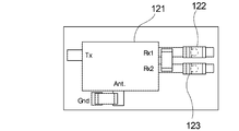
- the inductor chips 122 and 123 are arranged close to each other, the deterioration of the isolation characteristic becomes severe. Therefore, the inductor chips 122 and 123 cannot be arranged close to each other. Therefore, it is difficult to reduce the size of the high-frequency module.
- FIG. 5 is a schematic plan view of the high-frequency module according to the second embodiment.
Landscapes
- Physics & Mathematics (AREA)
- Acoustics & Sound (AREA)
- Transceivers (AREA)
- Surface Acoustic Wave Elements And Circuit Networks Thereof (AREA)
- Piezo-Electric Or Mechanical Vibrators, Or Delay Or Filter Circuits (AREA)
- Coils Or Transformers For Communication (AREA)
- Filters And Equalizers (AREA)
Abstract
Description
図1は、第1の実施形態に係る高周波モジュールの略図的回路図である。まず、図1を参照しながら、本実施形態の高周波モジュール1の回路構成について説明する。
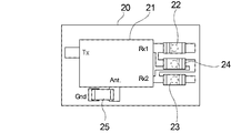
図5は、第2の実施形態に係る高周波モジュールの略図的平面図である。
上記実施形態では、高周波モジュールがひとつの分波器チップを備えている例について説明した。但し、本発明は、この構成に限定されない。本発明に係る高周波モジュールは、複数の分波器チップを備えていてもよい。また、本発明に係る高周波モジュールは、少なくともひとつの分波器チップに加え、他のフィルタチップを備えていてもよい。
本実施例では、上記第2の実施形態の高周波モジュールと実質的に同様の構成を有する高周波モジュールを作製した。なお、デュプレクサチップとしては、UMTS-Band5用のものを用いた。実施例1の高周波モジュールの送信側信号端子から受信側信号端子への差動アイソレーション特性を図6に示す。
比較例2では、インダクタチップ24の極性を逆にしたこと以外は、上記実施例1と同様の構成を有する高周波モジュールを作製した。インダクタチップ24の極性を逆にすることにより、受信フィルタ部16側から視て、インダクタチップ24の極性は、インダクタチップ22,23のいずれとも極性の向きが同じとなるように配置されている。比較例2の高周波モジュールの送信側信号端子から受信側信号端子への差動アイソレーション特性を図6に示す。
11…アンテナ側端子
12…送信側信号端子
13a…第1の受信側平衡信号端子
13b…第2の受信側平衡信号端子
15…送信フィルタ部
16…受信フィルタ部
16a…第1の平衡信号端子
16b…第2の平衡信号端子
20…実装基板
21…デュプレクサチップ
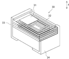
22~25,30…インダクタチップ
31…識別マーク
32…内部電極
33…第1の外部電極
34…第2の外部電極
L1~L6…インダクタ
Claims (6)
- アンテナ端子に接続されるアンテナ側端子と、
送信側信号端子と、
第1及び第2の受信側平衡信号端子と、
前記アンテナ端子と前記送信側信号端子との間に接続されている送信フィルタ部と、
前記アンテナ端子と前記第1及び第2の受信側平衡信号端子との間に接続されており、平衡-不平衡変換機能を有する受信フィルタ部と、
前記受信フィルタ部と前記第1または前記第2の受信側平衡信号端子との間に接続されている複数のインダクタと、
を備える高周波モジュールであって、
実装基板と、
前記実装基板の一主面上に実装されており、前記送信フィルタ部と前記受信フィルタ部とが設けられた分波器チップと、
前記実装基板の一主面上に実装されており、前記インダクタが設けられた複数のインダクタチップと、
を備え、
前記複数のインダクタチップのうち、隣接して配置されている2つのインダクタチップのそれぞれは、極性を有し、前記受信フィルタ部側から視て、極性の向きが逆となるように配置されている、高周波モジュール。 - 前記受信フィルタ部と前記第1の受信側平衡信号端子との間に接続されている第1のインダクタが設けられた第1のインダクタチップと、
前記受信フィルタ部と前記第2の受信側平衡信号端子との間に接続されている第2のインダクタが設けられた第2のインダクタチップとを備え、
前記第1及び第2のインダクタチップは、隣接して配置されている、請求項1に記載の高周波モジュール。 - 前記受信フィルタ部と前記第1の受信側平衡信号端子との間に接続されている第1のインダクタが設けられた第1のインダクタチップと、
前記受信フィルタ部と前記第2の受信側平衡信号端子との間に接続されている第2のインダクタが設けられた第2のインダクタチップと、
前記第1のインダクタと前記受信フィルタ部との間の接続点と、前記第2のインダクタと前記受信フィルタ部との間の接続点との間に接続されている第3のインダクタが設けられた第3のインダクタチップとを備え、
前記第1及び第3のインダクタチップが隣接して配置されており、且つ、
前記第2及び第3のインダクタチップが隣接して配置されている、請求項1または2に記載の高周波モジュール。 - 前記第3のインダクタチップは、前記受信フィルタ部側から視て、第1及び第2のインダクタチップのいずれとも極性の向きが逆となるように配置されている、請求項3に記載の高周波モジュール。
- 前記第3のインダクタチップは、前記第1のインダクタチップと前記第2のインダクタチップとの間に配置されている、請求項3または4に記載の高周波モジュール。
- 前記受信フィルタ部は、縦結合共振子型弾性波フィルタ部である、請求項1~5のいずれか一項に記載の高周波モジュール。
Priority Applications (4)
| Application Number | Priority Date | Filing Date | Title |
|---|---|---|---|
| DE112012000737.9T DE112012000737B4 (de) | 2011-02-09 | 2012-01-24 | Hochfrequenzmodul |
| CN201280007602.9A CN103339856B (zh) | 2011-02-09 | 2012-01-24 | 高频模块 |
| JP2012556818A JP5682635B2 (ja) | 2011-02-09 | 2012-01-24 | 高周波モジュール |
| US13/961,953 US9130540B2 (en) | 2011-02-09 | 2013-08-08 | High-frequency module having inductors disposed with directions of their polarities opposite to each other |
Applications Claiming Priority (2)
| Application Number | Priority Date | Filing Date | Title |
|---|---|---|---|
| JP2011-026092 | 2011-02-09 | ||
| JP2011026092 | 2011-02-09 |
Related Child Applications (1)
| Application Number | Title | Priority Date | Filing Date |
|---|---|---|---|
| US13/961,953 Continuation US9130540B2 (en) | 2011-02-09 | 2013-08-08 | High-frequency module having inductors disposed with directions of their polarities opposite to each other |
Publications (1)
| Publication Number | Publication Date |
|---|---|
| WO2012108254A1 true WO2012108254A1 (ja) | 2012-08-16 |
Family
ID=46638471
Family Applications (1)
| Application Number | Title | Priority Date | Filing Date |
|---|---|---|---|
| PCT/JP2012/051382 Ceased WO2012108254A1 (ja) | 2011-02-09 | 2012-01-24 | 高周波モジュール |
Country Status (5)
| Country | Link |
|---|---|
| US (1) | US9130540B2 (ja) |
| JP (1) | JP5682635B2 (ja) |
| CN (1) | CN103339856B (ja) |
| DE (1) | DE112012000737B4 (ja) |
| WO (1) | WO2012108254A1 (ja) |
Cited By (5)
| Publication number | Priority date | Publication date | Assignee | Title |
|---|---|---|---|---|
| WO2014061694A1 (ja) * | 2012-10-19 | 2014-04-24 | 株式会社村田製作所 | アンテナ分波器 |
| CN105453427A (zh) * | 2013-08-06 | 2016-03-30 | 株式会社村田制作所 | 高频模块 |
| WO2016181701A1 (ja) * | 2015-05-08 | 2016-11-17 | 株式会社村田製作所 | 高周波モジュール |
| CN114270714A (zh) * | 2019-08-28 | 2022-04-01 | 株式会社村田制作所 | 高频模块以及通信装置 |
| US20220349839A1 (en) * | 2019-07-12 | 2022-11-03 | Zte Corporation | Device for detecting sar, method for reducing sar, and mobile terminal |
Families Citing this family (3)
| Publication number | Priority date | Publication date | Assignee | Title |
|---|---|---|---|---|
| CN116783829A (zh) * | 2020-12-28 | 2023-09-19 | 株式会社村田制作所 | 滤波器装置、高频模块以及通信装置 |
| CN117063399A (zh) * | 2021-03-23 | 2023-11-14 | 株式会社村田制作所 | 复合滤波器装置 |
| US12562706B2 (en) | 2023-09-26 | 2026-02-24 | Apple Inc. | Isolation between filters using inductive coupling cancellation |
Citations (4)
| Publication number | Priority date | Publication date | Assignee | Title |
|---|---|---|---|---|
| JPS6428022U (ja) * | 1987-08-11 | 1989-02-17 | ||
| JP2002164704A (ja) * | 2000-11-28 | 2002-06-07 | Matsushita Electric Ind Co Ltd | バランス信号を扱う高周波スイッチ、スパイラルインダクタ及び分配器 |
| WO2007034589A1 (ja) * | 2005-09-26 | 2007-03-29 | Murata Manufacturing Co., Ltd. | 高周波フロントエンドモジュール及びデュプレクサ |
| JP2008167105A (ja) * | 2006-12-28 | 2008-07-17 | Hitachi Metals Ltd | 積層型バラントランス及び高周波部品 |
Family Cites Families (13)
| Publication number | Priority date | Publication date | Assignee | Title |
|---|---|---|---|---|
| DE3104270A1 (de) * | 1981-02-07 | 1982-09-02 | Vacuumschmelze Gmbh, 6450 Hanau | Funkentstoeranordnung und verfahren zur herstellung |
| US5754667A (en) * | 1995-01-25 | 1998-05-19 | Boston Acoustics, Inc. | Audio filter with magnetic field cancellation |
| JP4783996B2 (ja) * | 2001-05-02 | 2011-09-28 | 株式会社村田製作所 | 積層型複合バラントランス |
| JP3833569B2 (ja) * | 2001-12-21 | 2006-10-11 | 富士通メディアデバイス株式会社 | 分波器及びこれを用いた電子装置 |
| US6882250B2 (en) * | 2002-04-15 | 2005-04-19 | Matsushita Electric Industrial Co., Ltd. | High-frequency device and communication apparatus |
| CN1751436A (zh) * | 2003-12-01 | 2006-03-22 | 株式会社村田制作所 | 滤波器装置 |
| EP1729413B1 (en) * | 2004-03-16 | 2015-12-09 | Hitachi Metals, Ltd. | High-frequency circuit and high-frequency component |
| JP2006279604A (ja) | 2005-03-29 | 2006-10-12 | Tdk Corp | 弾性表面波装置 |
| JP4768398B2 (ja) | 2005-10-31 | 2011-09-07 | 京セラキンセキ株式会社 | ローパスフィルタ |
| JP4177389B2 (ja) | 2006-05-18 | 2008-11-05 | 富士通メディアデバイス株式会社 | フィルタおよび分波器 |
| CN101401304B (zh) | 2006-08-21 | 2011-04-13 | 株式会社村田制作所 | 高频模块 |
| CN102017408B (zh) * | 2008-05-07 | 2014-04-30 | 株式会社村田制作所 | 弹性波滤波装置 |
| KR101575387B1 (ko) * | 2009-03-18 | 2015-12-07 | 에이저 시스템즈 엘엘시 | 집적 회로 인덕터 구조체, 전자 시스템 및 집적 회로 인덕터 사이의 자기 커플링 감소 방법 |
-
2012
- 2012-01-24 WO PCT/JP2012/051382 patent/WO2012108254A1/ja not_active Ceased
- 2012-01-24 DE DE112012000737.9T patent/DE112012000737B4/de active Active
- 2012-01-24 JP JP2012556818A patent/JP5682635B2/ja active Active
- 2012-01-24 CN CN201280007602.9A patent/CN103339856B/zh active Active
-
2013
- 2013-08-08 US US13/961,953 patent/US9130540B2/en active Active
Patent Citations (4)
| Publication number | Priority date | Publication date | Assignee | Title |
|---|---|---|---|---|
| JPS6428022U (ja) * | 1987-08-11 | 1989-02-17 | ||
| JP2002164704A (ja) * | 2000-11-28 | 2002-06-07 | Matsushita Electric Ind Co Ltd | バランス信号を扱う高周波スイッチ、スパイラルインダクタ及び分配器 |
| WO2007034589A1 (ja) * | 2005-09-26 | 2007-03-29 | Murata Manufacturing Co., Ltd. | 高周波フロントエンドモジュール及びデュプレクサ |
| JP2008167105A (ja) * | 2006-12-28 | 2008-07-17 | Hitachi Metals Ltd | 積層型バラントランス及び高周波部品 |
Cited By (11)
| Publication number | Priority date | Publication date | Assignee | Title |
|---|---|---|---|---|
| WO2014061694A1 (ja) * | 2012-10-19 | 2014-04-24 | 株式会社村田製作所 | アンテナ分波器 |
| JPWO2014061694A1 (ja) * | 2012-10-19 | 2016-09-05 | 株式会社村田製作所 | アンテナ分波器 |
| CN105453427A (zh) * | 2013-08-06 | 2016-03-30 | 株式会社村田制作所 | 高频模块 |
| CN105453427B (zh) * | 2013-08-06 | 2018-02-09 | 株式会社村田制作所 | 高频模块 |
| WO2016181701A1 (ja) * | 2015-05-08 | 2016-11-17 | 株式会社村田製作所 | 高周波モジュール |
| JPWO2016181701A1 (ja) * | 2015-05-08 | 2018-02-01 | 株式会社村田製作所 | 高周波モジュール |
| US10439588B2 (en) | 2015-05-08 | 2019-10-08 | Murata Manufacturing Co., Ltd. | High frequency module |
| US20220349839A1 (en) * | 2019-07-12 | 2022-11-03 | Zte Corporation | Device for detecting sar, method for reducing sar, and mobile terminal |
| US12320760B2 (en) * | 2019-07-12 | 2025-06-03 | Zte Corporation | Device for detecting SAR, method for reducing SAR, and mobile terminal |
| CN114270714A (zh) * | 2019-08-28 | 2022-04-01 | 株式会社村田制作所 | 高频模块以及通信装置 |
| CN114270714B (zh) * | 2019-08-28 | 2024-01-05 | 株式会社村田制作所 | 高频模块以及通信装置 |
Also Published As
| Publication number | Publication date |
|---|---|
| CN103339856B (zh) | 2016-03-02 |
| DE112012000737T5 (de) | 2013-11-14 |
| JP5682635B2 (ja) | 2015-03-11 |
| CN103339856A (zh) | 2013-10-02 |
| US9130540B2 (en) | 2015-09-08 |
| US20140009240A1 (en) | 2014-01-09 |
| DE112012000737B4 (de) | 2018-02-15 |
| JPWO2012108254A1 (ja) | 2014-07-03 |
Similar Documents
| Publication | Publication Date | Title |
|---|---|---|
| JP5682635B2 (ja) | 高周波モジュール | |
| JP5677499B2 (ja) | 高周波回路モジュール | |
| JP6668213B2 (ja) | 分波器と通信機器 | |
| JP5075209B2 (ja) | デュプレクサ、およびデュプレクサを含むモジュール、通信機器 | |
| JP6249020B2 (ja) | 高周波モジュール | |
| JPWO2016181701A1 (ja) | 高周波モジュール | |
| JP2009021895A (ja) | アンテナ共用器とそれを用いた通信機器 | |
| JPWO2013021626A1 (ja) | フィルタモジュール | |
| JP6832871B2 (ja) | マルチプレクサ | |
| JP5700121B2 (ja) | 弾性波フィルタ装置 | |
| CN107431478B (zh) | 双工器 | |
| CN104604130A (zh) | 弹性波滤波器装置及双工器 | |
| JP5590135B2 (ja) | 高周波モジュール | |
| CN103404040A (zh) | 高频开关模块 | |
| CN103141025A (zh) | 弹性波滤波器装置 | |
| JP2019192992A (ja) | フロントエンドモジュールおよび通信装置 | |
| CN111386656B (zh) | 多工器 | |
| US8912866B2 (en) | Dual-band surface acoustic wave filter and composite high-frequency component | |
| WO2011077773A1 (ja) | 分波器 | |
| JP5660223B2 (ja) | 分波装置 | |
| WO2015098240A1 (ja) | フィルタ装置およびデュプレクサ | |
| WO2012176576A1 (ja) | フィルタ装置 | |
| JP5234069B2 (ja) | 磁気共鳴型アイソレータ | |
| JP5573947B2 (ja) | 回路モジュール | |
| JP2013098507A (ja) | 高周波電子部品 |
Legal Events
| Date | Code | Title | Description |
|---|---|---|---|
| 121 | Ep: the epo has been informed by wipo that ep was designated in this application |
Ref document number: 12744678 Country of ref document: EP Kind code of ref document: A1 |
|
| ENP | Entry into the national phase |
Ref document number: 2012556818 Country of ref document: JP Kind code of ref document: A |
|
| WWE | Wipo information: entry into national phase |
Ref document number: 1120120007379 Country of ref document: DE Ref document number: 112012000737 Country of ref document: DE |
|
| 122 | Ep: pct application non-entry in european phase |
Ref document number: 12744678 Country of ref document: EP Kind code of ref document: A1 |