WO2012105229A1 - 耐湿熱膜とその製造方法、デバイス、及び太陽電池 - Google Patents
耐湿熱膜とその製造方法、デバイス、及び太陽電池 Download PDFInfo
- Publication number
- WO2012105229A1 WO2012105229A1 PCT/JP2012/000601 JP2012000601W WO2012105229A1 WO 2012105229 A1 WO2012105229 A1 WO 2012105229A1 JP 2012000601 W JP2012000601 W JP 2012000601W WO 2012105229 A1 WO2012105229 A1 WO 2012105229A1
- Authority
- WO
- WIPO (PCT)
- Prior art keywords
- indium
- moisture
- heat
- film
- resistant film
- Prior art date
- Legal status (The legal status is an assumption and is not a legal conclusion. Google has not performed a legal analysis and makes no representation as to the accuracy of the status listed.)
- Ceased
Links
Images

Classifications
-
- H—ELECTRICITY
- H10—SEMICONDUCTOR DEVICES; ELECTRIC SOLID-STATE DEVICES NOT OTHERWISE PROVIDED FOR
- H10F—INORGANIC SEMICONDUCTOR DEVICES SENSITIVE TO INFRARED RADIATION, LIGHT, ELECTROMAGNETIC RADIATION OF SHORTER WAVELENGTH OR CORPUSCULAR RADIATION
- H10F77/00—Constructional details of devices covered by this subclass
- H10F77/20—Electrodes
- H10F77/244—Electrodes made of transparent conductive layers, e.g. transparent conductive oxide [TCO] layers
- H10F77/251—Electrodes made of transparent conductive layers, e.g. transparent conductive oxide [TCO] layers comprising zinc oxide [ZnO]
Definitions
- the present invention relates to a moisture-resistant heat-resistant film that is a light-transmitting conductive film having heat-and-moisture resistance, a manufacturing method thereof, a device such as a photoelectric conversion element provided with a light-transmitting electrode layer comprising the moisture-resistant heat film, and a photoelectric conversion element.
- the solar cell a moisture-resistant heat-resistant film that is a light-transmitting conductive film having heat-and-moisture resistance
- the chalcopyrite compound semiconductor is a compound represented by the general formula LMX 2 (L represents at least one group IB element, M represents at least one group IIIB, and X represents at least one group VIB).
- L is at least one selected from the group consisting of Cu, Ag, and Au.
- M is preferably at least one selected from the group consisting of Al, Ga, and In.
- X is preferably at least one selected from the group consisting of S, Se, and Te.
- CIS CuInSe 2
- Cu In, Ga) Se 2
- CIGS Cu (In, Ga) Se 2
- CIS and CIGS are collectively referred to as a CI (G) S system.
- CI (G) S-based chalcopyrite compound semiconductors can be made lighter than conventional solar cells using silicon, and can be manufactured at low cost because material costs can be reduced. It has the advantage that it can be used (Non-Patent Document 1, etc.).
- a photoelectric conversion element using a chalcopyrite compound semiconductor as a light absorption layer a back electrode layer, a light absorption layer, a buffer layer, a translucent high resistance layer, and a low resistance translucent electrode layer are sequentially laminated on a substrate.
- the basic structure As a material for the low-resistance translucent electrode layer, a material having high light transmittance and low resistance is used. Suitable materials include indium tin oxide (ITO), indium zinc oxide (IZO) preferably containing 55 to 75 mol% indium, and zinc oxide ZnO. These may be doped with various metals.
- ITO indium tin oxide
- IZO indium zinc oxide
- ZnO zinc oxide
- a windshield that does not substantially transmit moisture is provided to protect the inside of the element.
- this windshield is the most expensive member in solar cells.
- it is difficult to reduce the weight of the entire solar cell due to the windshield.
- ZnO which is relatively inexpensive, is known to have low heat and humidity resistance, and its conductivity is lowered in a high temperature and high humidity environment. Therefore, when a ZnO film is used as the translucent electrode layer, a moisture barrier structure such as a windshield is essential.
- ITO and IZO have high heat-and-moisture resistance and can maintain performance even in a high-temperature and high-humidity environment.
- ITO and IZO have a high amount of expensive indium and are expensive.
- the present invention has been made in view of the above circumstances, and provides a moisture-resistant and heat-resistant film comprising a light-transmitting conductive film containing ZnO, in which a decrease in conductivity in a high-temperature and high-humidity environment is suppressed, and a method for manufacturing the same. It is intended.
- the present invention also provides a device such as a low-cost photoelectric conversion element that does not require a moisture barrier structure on the external environment side of the translucent electrode layer by using the moisture-resistant heat resistant film as the translucent electrode layer. It is for the purpose.
- the moisture and heat resistant film of the present invention is Ra / Rb, which is the ratio between the sheet resistance value Ra after 1000 hours in an environment of 85 ° C. and 85% relative humidity and the sheet resistance value Rb immediately before exposure to the environment, is 0.9 to 5.0.
- Ra / Rb is the ratio between the sheet resistance value Ra after 1000 hours in an environment of 85 ° C. and 85% relative humidity and the sheet resistance value Rb immediately before exposure to the environment.
- Has some heat and humidity resistance It is a translucent conductive film containing indium-doped zinc oxide in which 1.5 mol% or more of indium is doped with respect to zinc oxide.
- IZO indium zinc oxide
- IZO contains an indium element, a zinc element, and an oxygen element, but forms a compound as IZO containing indium exceeding the doping level, and does not show the crystal form of ZnO.
- the moisture-resistant heat resistant film of the present invention preferably contains indium-doped zinc oxide having Ra / Rb of 0.9 to 1.1 and doped with 2.0 mol% or more of indium with respect to zinc oxide. .
- the method for producing the moisture and heat resistant film of the present invention comprises: A method for producing the moisture and heat resistant film of the present invention as described above, A step (A) of forming a precursor film by forming a precursor composition containing zinc and / or a zinc compound and indium and / or an indium compound on a substrate; and And (B) generating the indium-doped zinc oxide by heating the precursor film.
- the device of the present invention is provided with the translucent electrode layer comprising the above-described heat and moisture resistant film of the present invention.
- the device of the present invention can be applied to a photoelectric conversion element provided with a semiconductor light absorption layer.
- the photoelectric conversion element can be used for solar cells and the like.
- the present invention consists of a translucent electrically conductive film containing ZnO, and can provide the heat-and-moisture resistant film in which the fall of the conductivity in a high temperature, high humidity environment was suppressed, and its manufacturing method.
- a low-cost device such as a photoelectric conversion element that does not require a moisture barrier structure on the external environment side of the translucent electrode layer is provided by using the moisture resistant heat resistant film as the translucent electrode layer. can do.
- Heat and heat resistant film The present inventors have found that doping ZnO film with 1.5 mol% or more of In improves the wet heat resistance of ZnO and suppresses the decrease in conductivity in a high temperature and high humidity environment.
- the present invention has been completed (see the “Examples” section below). Specifically, by doping In to 1.5 mol% or more of ZnO film, the sheet resistance value Ra after 1000 hours in an environment of 85 ° C. and a relative humidity of 85%, and the sheet immediately before being exposed to the environment It has been found that moisture / heat resistance having a ratio Ra / Rb of 0.9 to 5.0, which is a ratio to the resistance value Rb, can be obtained.
- the present inventor has found that, particularly when the ZnO film is doped with 2.0 mol% or more of In, heat / heat resistance with Ra / Rb of 0.9 to 1.1 can be obtained.
- the moisture and heat resistant film of the present invention is Ra / Rb, which is the ratio between the sheet resistance value Ra after 1000 hours in an environment of 85 ° C. and 85% relative humidity and the sheet resistance value Rb immediately before exposure to the environment, is 0.9 to 5.0.
- Ra / Rb is the ratio between the sheet resistance value Ra after 1000 hours in an environment of 85 ° C. and 85% relative humidity and the sheet resistance value Rb immediately before exposure to the environment.
- Has some heat and humidity resistance It is a translucent conductive film containing indium-doped zinc oxide in which 1.5 mol% or more of indium is doped with respect to zinc oxide.
- the upper limit of the amount of In doping with respect to ZnO is not particularly limited, and [Example] confirms that good wet heat resistance can be obtained in the range of at least 1.5 to 5.0 mol%. If the amount of In doping with respect to ZnO increases too much, the cost increases. Therefore, the upper limit of the amount of In doping with respect to ZnO is preferably 5.0 mol%, and more preferably 2.5 mol%. On the other hand, if the amount of In doping with respect to ZnO becomes too small, the heat and moisture resistance may be insufficient.
- the lower limit of the amount of In doping with respect to ZnO is 1.5 mol%, preferably 1.7 mol%, preferably 2.0 mol%. More preferred.
- the heat and moisture resistant film of the present invention preferably contains indium-doped zinc oxide doped with 1.5 to 5.0 mol% indium with respect to zinc oxide, and 2.0 to 5 indium with respect to zinc oxide. It is particularly preferred to contain 0.0 mol% doped indium doped zinc oxide.
- the moisture and heat resistant film of the present invention can be used as a translucent electrode layer of a photoelectric conversion element.
- zinc oxide may be doped with a metal element other than indium. If it is for a translucent electrode layer of a photoelectric conversion element, the doping element of zinc oxide includes gallium, aluminum, boron, silicon, tin, indium, germanium, antimony, iridium, rhenium, cerium, zirconium, scandium, yttrium, And lanthanoids. Zinc oxide can be doped with at least one of these, for example, 0.05 to 15 mol%.
- the moisture and heat resistant film of the present invention contains indium-doped zinc oxide as an essential component, and further has other translucency such as indium tin oxide (ITO) or indium zinc oxide (IZO) preferably containing 55 to 75 mol% indium.
- ITO indium tin oxide
- IZO indium zinc oxide
- a conductive material can be included.
- ITO and IZO have a large amount of expensive indium and are expensive. Therefore, the higher the ZnO content, the lower the cost and the better.
- the moisture and heat resistant film of the present invention particularly preferably contains 50% by mass or more of indium-doped zinc oxide.
- the method for producing the moisture and heat resistant film of the present invention is not limited.
- Examples of the method for producing a heat and moisture resistant film of the present invention include sputtering, electron beam vapor deposition, ion plating, molecular beam epitaxy, ionization vapor deposition, laser ablation, arc plasma vapor deposition, thermal CVD, and plasma CVD.
- Methods, MOCVD methods, spray pyrolysis methods, sol-gel methods, electroless plating methods, electrolytic plating methods, coating and baking methods, aerosol deposition methods, fine particle coating methods, and the like can be applied.
- the moisture and heat resistant film of the present invention is, for example, A step (A) of forming a precursor film by forming a precursor composition containing zinc and / or a zinc compound and indium and / or an indium compound on a substrate; and
- the precursor film can be manufactured by a manufacturing method including a step (B) of generating indium-doped zinc oxide by heating the precursor film.
- the method for forming the precursor film is not particularly limited, and examples thereof include coating and spraying.
- the present inventor has produced a moisture and heat resistant film by spray pyrolysis.
- the step (A) is a step of forming a precursor film by spraying the precursor composition together with a carrier gas on the substrate.
- the precursor composition may be a composition that finally produces indium-doped zinc oxide.
- the precursor composition preferably contains a solvent.
- the solvent is not particularly limited, and an organic solvent, an inorganic solvent such as water, or an organic / inorganic mixed solvent can be used. Considering the environmental impact, cost, solution environment suitable for complex formation necessary for the production of indium-doped zinc oxide, solubility, etc., the precursor composition is composed of zinc and / or zinc compound, indium and / or An aqueous solution containing an indium compound is preferable.
- the precursor composition preferably contains 5.0 to 50.0 vol% acetic acid.
- the precursor composition can include zinc acetate and indium acetate and / or an acetylacetonate salt of indium.
- the precursor composition contains these metal compounds themselves or these precursors.
- the precursor composition may contain additives such as a pH adjuster or a dispersant as long as the effects of the present invention are not impaired.
- the heating temperature in the step (B) of heating the precursor film to produce indium-doped zinc oxide is not particularly limited, and when the moisture-resistant heat resistant film is mainly composed of indium-doped zinc oxide, it is preferably 255 to 600 ° C., 300 More preferred is ⁇ 500 ° C.
- the present invention it is possible to provide a moisture and heat resistant film made of a light-transmitting conductive film containing ZnO and suppressed in a high-temperature and high-humidity environment, and a manufacturing method thereof.
- the moisture and heat resistant film of the present invention can be used as a translucent electrode layer of various devices.
- the device of the present invention is provided with the translucent electrode layer comprising the above-described heat and moisture resistant film of the present invention. Since the moisture-and-heat-resistant film of the present invention has good heat-and-moisture resistance, the device of the present invention includes a moisture barrier layer and a moisture barrier member that do not substantially transmit moisture to the external environment side of the translucent electrode layer. Does not require a moisture barrier structure.
- “substantially does not transmit moisture” is defined as having a water vapor permeability of 10 ⁇ 2 g / m 2 / day or less.
- the device of the present invention does not require an expensive and heavy windshield on the external environment side of the translucent electrode layer.
- an inexpensive resin film can be used instead of a conventionally used windshield as a protective material for the device.
- the device of the present invention includes a translucent electrode layer using relatively inexpensive ZnO and does not require a moisture barrier member such as a moisture barrier layer and an expensive windshield, so that the cost can be reduced.
- the device of the present invention described above can be applied to a photoelectric conversion element or the like provided with a semiconductor light absorption layer.
- the semiconductor light absorption layer is a layer made of a semiconductor capable of photoelectric conversion.
- the composition of the semiconductor light-absorbing layer is not limited, and high efficiency is expected with a thin film. Therefore, it is selected from the group consisting of chalcopyrite type compound semiconductors, kesterite type compound semiconductors, stannite type compound semiconductors, and II-VI group semiconductors. It is preferable that at least one semiconductor is included.
- FIG. 1 is a cross-sectional view, and in order to facilitate visual recognition, the actual scales of the layers are appropriately changed.
- the semiconductor light absorption layer is made of a chalcopyrite compound semiconductor (the semiconductor light absorption layer may contain inevitable impurities), and a photoelectric conversion element will be described as an example.
- the photoelectric conversion element 10 of the present embodiment includes a back electrode layer 12, a semiconductor light absorption layer (p-type semiconductor layer) 13, a buffer layer (n-type semiconductor layer) 14, a translucent high resistance layer 15, on a substrate 11.
- the transparent electrode layer 16 is sequentially laminated.
- the translucent high resistance layer 15 is a layer provided as necessary, and is not essential.
- extraction electrodes 17 and 18 are provided on the back electrode layer 12 and the translucent electrode layer 16 as necessary.
- light and electricity are converted by generating electrons and holes when light is applied to the interface between the p-type semiconductor and the n-type semiconductor.
- the type of the substrate 11 is not limited and a glass substrate is generally used.
- a flexible film such as a resin film such as PET (polyethylene terephthalate) or polyimide, or a metal foil such as aluminum or stainless steel may be used.
- a metal foil such as aluminum or stainless steel
- an insulating film is necessary on the substrate surface.
- an alkali metal such as Na and / or an alkaline earth metal such as Mg is supplied from the substrate side during the formation of the light absorption layer, the crystallinity of the film is improved and photoelectric conversion is performed. It is known to improve efficiency.
- a substrate containing Na such as blue plate glass is used, or an alkali (earth) metal supply layer such as sodium halide is formed between the above-mentioned substrate not containing Na and the light absorption layer 13 by a known method. Also good.
- a known material can be applied to the back electrode layer 12 as long as it can make ohmic contact with the light absorption layer 13.
- a known material include gold, molybdenum, nickel, titanium, tantalum, and combinations thereof. Among them, molybdenum and the like are preferably applied because they are inexpensive and easily available.
- a known method can be applied, and a sputtering method, a heat evaporation method, an electrolytic plating method, an electroless plating method, or the like can be applied.
- the semiconductor light absorption layer 13 is a p-type compound semiconductor film made of at least one chalcopyrite compound semiconductor represented by the following general formula (i).
- LMX 2 (wherein L represents at least one group IB element, M represents at least one group IIIB, and X represents at least one group VIB.)
- L include Cu, Ag, and Au.
- M include Al, Ga, and In.
- X include O, S, Se, and Te.
- the semiconductor light absorption layer 13 is preferably made of at least one compound semiconductor represented by the following general formula (ii), and at least one kind represented by the following general formula (iii) More preferably, it is made of a compound semiconductor.
- L1 (M1) (X1) 2 (where L1 is at least one IB group element selected from the group consisting of Cu, Ag, and Au, and M1 is selected from the group consisting of Al, Ga, and In) At least one group IIIB, X1 represents at least one group VIB selected from the group consisting of S, Se, and Te.) (Ii), (L2) (M2) (X2) 2 (where L2 is at least one group IB element containing Cu, M2 is at least one group IIIB containing Ga and / or In, and X2 is at least one containing Se) Each represents a VIB family of species.) ... (iii)
- Examples of the compound semiconductor represented by the formula (iii) include CuInSe 2 (CIS) and Cu (In, Ga) Se 2 (CIGS). These CI (G) S systems have a matching band gap, a high light absorption coefficient, and a high photoelectric conversion efficiency can be obtained with a thin film.
- the light absorption layer 13 is thicker because more carriers can be generated because light absorption can be increased.
- the p-type semiconductor layer also functions as a resistance component, it is preferable that the film thickness is small from the viewpoint of efficient extraction of generated carriers. Considering both, the film thickness of the light absorption layer 13 is preferably 0.5 to 10 ⁇ m, more preferably 1 to 5 ⁇ m, and further preferably 1.5 to 3 ⁇ m.
- the buffer layer 14 formed on the light absorption layer 13 is an n-type semiconductor layer.
- a II-VI group compound and / or a III-VI group compound are mainly applied.
- Cd (S, O), Zn (S, O), In (S, O), InSe, and the like are applied as known substances. These compounds may contain a trace amount of hydroxide and the like.
- the buffer layer 14 can be formed by a chemical bath deposition method (CBD method: Chemical Bath Deposition method), a sputtering method, or the like.
- the light absorption layer is adjusted at a temperature at which CdS is precipitated by adjusting an aqueous solution containing a cadmium salt (for example, cadmium iodide) and a sulfur-containing compound (for example, thiourea) to a pH at which sulfur is dissociated.
- a cadmium salt for example, cadmium iodide
- a sulfur-containing compound for example, thiourea
- the thickness of the buffer layer 14 is preferably 1 to 300 nm, more preferably 10 to 200 nm, and still more preferably 20 to 150 nm.
- the high resistance film 15 can be introduced on the buffer layer 14 as necessary.
- the material of the high resistance film 15 include ZnO.
- the film thickness of the high resistance film is thick, it leads to a loss in carrier transmission due to an increase in the series resistance component. Therefore, the film thickness is preferably 100 nm or less.
- the translucent electrode layer 16 is composed of the above-described moisture and heat resistant film of the present invention.
- the film thickness of the translucent electrode layer 16 is thick, the light transmittance is lowered, which leads to a decrease in the number of carriers generated.
- the film thickness is small, the resistance component up to the extraction electrode 18 is increased, which leads to loss during carrier transmission, which is not preferable.
- the film thickness of the translucent electrode layer 16 is preferably 10 to 1000 nm, more preferably 100 to 700 nm, and still more preferably 200 to 500 nm.
- the extraction electrodes 17 and 18 may be provided on the back electrode layer 12 and the translucent electrode layer 16 for the purpose of reducing the contact resistance when the carriers generated in the photoelectric conversion element 10 are taken out to the external circuit.
- the extraction electrode 17/18 is not limited as long as it has a low resistance that can form an ohmic contact with the back electrode layer 12 / translucent electrode 16.
- gold or aluminum is deposited by sputtering or vapor deposition. it can.
- the photoelectric conversion element 10 of this embodiment can be provided with arbitrary layers other than the above as needed.
- the photoelectric conversion element 10 of the present embodiment includes the translucent electrode layer 16 made of the above-described moisture and heat resistant film of the present invention, a moisture barrier member such as a moisture barrier layer and an expensive windshield is essential. Therefore, cost reduction can be achieved.
- the photoelectric conversion element 10 can be used as a solar cell or the like.
- Example 1 Zinc acetate (15.4 g) and indium acetate (Xmg) were dissolved in a 20 vol% acetic acid aqueous solution (100 mL) to prepare a plurality of types of spray liquids (precursor compositions) having different amounts of indium acetate.
- concentration in () has shown In amount with respect to Zn in a spray liquid. The present inventor has confirmed that the amount of In with respect to Zn is substantially the same between the charged composition and the final film composition.
- a borosilicate glass substrate having a length of 25 mm, a width of 25 mm, and a thickness of 1 mm was placed on a hot plate, and the substrate surface temperature was kept at 500 ° C.
- a film was formed on this substrate by spraying the spray solution from above 30 cm above the substrate using a commercially available spray device. In this step, since heating is performed simultaneously with spraying, the target product is generated from the precursor, and unnecessary solvents such as water are removed. Nitrogen was used as a carrier gas for spraying.
- the spray liquid discharge flow rate was 4 mL / min
- the carrier gas (nitrogen) flow rate was 10 L / min
- the spray time was 8 minutes.
- the sheet resistance of the film was measured using “Loresta EP” manufactured by Mitsubishi Chemical Corporation. Thereafter, the substrate was stored in an environment of 85 ° C. and 85% relative humidity using “Environmental Tester SH-221” manufactured by Espec. After exposure to an 85 ° C. and 85% environment, the change in sheet resistance of the film was measured over time over 1000 hours.
- Table 1 shows the measurement results of sheet resistance Rb before exposure to high temperature and high humidity, sheet resistance Ra [ ⁇ / ⁇ ] after elapse of 1000 hours, and Ra / Rb.
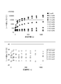
- FIG. 2 shows measurement results of sheet resistance with time for an example using zinc and a spray solution containing 2 to 5 mol% indium with respect to zinc. From the results shown in FIG.
- high temperature and high humidity environment can be obtained by using zinc and a spray liquid containing 1.5 to 5.0 mol%, preferably 2.0 to 5.0 mol% of indium with respect to zinc. It became clear that a translucent conductive film having a small change in sheet resistance was obtained even below.
- the moisture and heat resistant film of the present invention can be used as a translucent electrode layer of a device such as a photoelectric conversion element. Since the photoelectric conversion element of the present invention has high conversion efficiency between light and electricity and can be manufactured at low cost, it can be used as a photoelectric conversion element such as a solar cell, an optical sensor, an image sensor, and a photodiode.
Landscapes
- Photovoltaic Devices (AREA)
- Manufacturing Of Electric Cables (AREA)
- Inorganic Compounds Of Heavy Metals (AREA)
- Non-Insulated Conductors (AREA)
Abstract
ZnOを含む透光性導電膜からなり、高温高湿環境下における伝導性の低下が抑制された耐湿熱膜を提供する。本発明の耐湿熱膜は、85℃相対湿度85%の環境下において1000時間経過した後のシート抵抗値Raと、前記環境下に曝す直前のシート抵抗値Rbとの比であるRa/Rbが0.9~5.0である耐湿熱性を有し、酸化亜鉛に対してインジウムが1.5mol%以上ドープされたインジウムドープ酸化亜鉛を含む透光性導電膜である。
Description
本発明は、耐湿熱性を有する透光性導電膜である耐湿熱膜とその製造方法、この耐湿熱膜からなる透光性電極層を備えた光電変換素子等のデバイス、及び光電変換素子を用いた太陽電池に関するものである。
カルコパイライト系化合物半導体は、一般式LMX2(Lは少なくとも1種のIB族元素、Mは少なくとも1種のIIIB族、Xは少なくとも1種のVIB族を各々示す。)で表わされる化合物である。
LはCu,Ag,及びAuからなる群より選ばれた少なくとも1種である。MはAl,Ga,及びInからなる群より選ばれた少なくとも1種が好ましい。XはS,Se,及びTeからなる群より選ばれた少なくとも1種が好ましい。
LはCu,Ag,及びAuからなる群より選ばれた少なくとも1種である。MはAl,Ga,及びInからなる群より選ばれた少なくとも1種が好ましい。XはS,Se,及びTeからなる群より選ばれた少なくとも1種が好ましい。
上記カルコパイライト系化合物半導体の中でも、CuInSe2(CIS)及びCu(In,Ga)Se2(CIGS)等は直接遷移型の吸収係数を示すため、薄膜で高光電変換効率が得られることが期待され、太陽電池の光吸収層材料として研究されている。本明細書では、「CIS及びCIGS」を合わせてCI(G)S系と称す。
CI(G)S系等のカルコパイライト系化合物半導体は、従来のシリコンを用いた太陽電池と比較して、軽量化ができること、材料コストを抑えることができるため低コストで製造できること、フレキシブル基板を使用できること等の利点を有する(非特許文献1等)。
CI(G)S系等のカルコパイライト系化合物半導体は、従来のシリコンを用いた太陽電池と比較して、軽量化ができること、材料コストを抑えることができるため低コストで製造できること、フレキシブル基板を使用できること等の利点を有する(非特許文献1等)。
カルコパイライト系化合物半導体を光吸収層とする光電変換素子は、基板上に裏面電極層と光吸収層とバッファ層と透光性高抵抗層と低抵抗の透光性電極層とが順次積層された構造を基本構造としている。
低抵抗の透光性電極層の材料としては、光の透過率が高く、抵抗が低いものが用いられる。その好適な材料としては、インジウム錫酸化物(ITO)、インジウムを好ましくは55~75mol%含むインジウム亜鉛酸化物(IZO)、及び酸化亜鉛ZnO等が挙げられる。これらには、各種金属がドープされてもよい。
低抵抗の透光性電極層の材料としては、光の透過率が高く、抵抗が低いものが用いられる。その好適な材料としては、インジウム錫酸化物(ITO)、インジウムを好ましくは55~75mol%含むインジウム亜鉛酸化物(IZO)、及び酸化亜鉛ZnO等が挙げられる。これらには、各種金属がドープされてもよい。
化合物薄膜太陽電池の最新技術(シーエムシー出版、2007年、和田隆博)
通常、太陽電池では、光電変換素子の水分による劣化を防止するために、実質的に水分を透過しないフロントガラスを設けて素子内部を保護している。しかしながら、このフロントガラスは、太陽電池において最も高コストな部材である。また、フロントガラスによって太陽電池全体の軽量化も難しい。
上記の透光性電極層の材料の中で、比較的安価なZnOは耐湿熱性が低く、高温高湿環境下において伝導性が低下することが知られていている。そのため、透光性電極層としてZnO膜を用いる場合には、フロントガラス等の水分バリア構造が必須である。
ITO及びIZOは耐湿熱性が高く、高温高湿環境下においても性能を維持できる。しかしながら、ITO及びIZOは高価なインジウム量が多く、高コストである。
ITO及びIZOは耐湿熱性が高く、高温高湿環境下においても性能を維持できる。しかしながら、ITO及びIZOは高価なインジウム量が多く、高コストである。
本発明は上記事情に鑑みてなされたものであり、ZnOを含む透光性導電膜からなり、高温高湿環境下における伝導性の低下が抑制された耐湿熱膜とその製造方法を提供することを目的とするものである。
本発明はまた、上記耐湿熱膜を透光性電極層として用いることにより、透光性電極層の外部環境側に水分バリア構造を必須としない、低コストな光電変換素子等のデバイスを提供することを目的とするものである。
本発明はまた、上記耐湿熱膜を透光性電極層として用いることにより、透光性電極層の外部環境側に水分バリア構造を必須としない、低コストな光電変換素子等のデバイスを提供することを目的とするものである。
本発明の耐湿熱膜は、
85℃相対湿度85%の環境下において1000時間経過した後のシート抵抗値Raと、前記環境下に曝す直前のシート抵抗値Rbとの比であるRa/Rbが0.9~5.0である耐湿熱性を有し、
酸化亜鉛に対してインジウムが1.5mol%以上ドープされたインジウムドープ酸化亜鉛を含む透光性導電膜である。
85℃相対湿度85%の環境下において1000時間経過した後のシート抵抗値Raと、前記環境下に曝す直前のシート抵抗値Rbとの比であるRa/Rbが0.9~5.0である耐湿熱性を有し、
酸化亜鉛に対してインジウムが1.5mol%以上ドープされたインジウムドープ酸化亜鉛を含む透光性導電膜である。
ここで、「ドープ」とは、ドーパントであるインジウムをZnOの結晶型が変わらない範囲で添加することを示す。例えば、インジウム亜鉛酸化物(IZO)は、インジウム元素と亜鉛元素と酸素元素を含んでいるが、インジウムがドープのレベルを超えて含まれたIZOとして化合物をなし、ZnOの結晶型を示さないので、インジウムドープ酸化亜鉛ではない。
本発明の耐湿熱膜において、前記Ra/Rbが0.9~1.1である耐熱性を有し、酸化亜鉛に対するインジウムが2.0mol%以上ドープされたインジウムドープ酸化亜鉛を含むことが好ましい。
本発明の耐湿熱膜の製造方法は、
上記の本発明の耐湿熱膜の製造方法であって、
基材上に、亜鉛及び/又は亜鉛化合物と、インジウム及び/又はインジウム化合物とを含む前駆体組成物を成膜して前駆体膜を形成する工程(A)と、
前記前駆体膜を加熱してインジウムドープ酸化亜鉛を生成する工程(B)とを有するものである。
上記の本発明の耐湿熱膜の製造方法であって、
基材上に、亜鉛及び/又は亜鉛化合物と、インジウム及び/又はインジウム化合物とを含む前駆体組成物を成膜して前駆体膜を形成する工程(A)と、
前記前駆体膜を加熱してインジウムドープ酸化亜鉛を生成する工程(B)とを有するものである。
本発明のデバイスは、上記の本発明の耐湿熱膜からなる透光性電極層を備えたものである。
本発明のデバイスは、半導体光吸収層を備えた光電変換素子等に適用できる。光電変換素子は太陽電池等に利用できる。
本発明のデバイスは、半導体光吸収層を備えた光電変換素子等に適用できる。光電変換素子は太陽電池等に利用できる。
本発明によれば、ZnOを含む透光性導電膜からなり、高温高湿環境下における伝導性の低下が抑制された耐湿熱膜とその製造方法を提供することができる。
本発明によれば、上記耐湿熱膜を透光性電極層として用いることにより、透光性電極層の外部環境側に水分バリア構造を必須としない、低コストな光電変換素子等のデバイスを提供することができる。
本発明によれば、上記耐湿熱膜を透光性電極層として用いることにより、透光性電極層の外部環境側に水分バリア構造を必須としない、低コストな光電変換素子等のデバイスを提供することができる。
「耐湿熱膜」
本発明者は、ZnO膜にInを1.5mol%以上ドープすることにより、ZnOの耐湿熱性が向上して、高温高湿環境下において伝導性が低下することが抑制されることを見出して、本発明を完成した(後記[実施例]の項を参照)。
具体的には、ZnO膜にInを1.5mol%以上ドープすることにより、85℃相対湿度85%の環境下において1000時間経過した後のシート抵抗値Raと、前記環境下に曝す直前のシート抵抗値Rbとの比であるRa/Rbが0.9~5.0である耐湿熱性が得られることを見出した。本発明者は、特に、ZnO膜にInを2.0mol%以上ドープした場合、Ra/Rbが0.9~1.1である耐湿熱性が得られることを見出した。
本発明者は、ZnO膜にInを1.5mol%以上ドープすることにより、ZnOの耐湿熱性が向上して、高温高湿環境下において伝導性が低下することが抑制されることを見出して、本発明を完成した(後記[実施例]の項を参照)。
具体的には、ZnO膜にInを1.5mol%以上ドープすることにより、85℃相対湿度85%の環境下において1000時間経過した後のシート抵抗値Raと、前記環境下に曝す直前のシート抵抗値Rbとの比であるRa/Rbが0.9~5.0である耐湿熱性が得られることを見出した。本発明者は、特に、ZnO膜にInを2.0mol%以上ドープした場合、Ra/Rbが0.9~1.1である耐湿熱性が得られることを見出した。
本発明の耐湿熱膜は、
85℃相対湿度85%の環境下において1000時間経過した後のシート抵抗値Raと、前記環境下に曝す直前のシート抵抗値Rbとの比であるRa/Rbが0.9~5.0である耐湿熱性を有し、
酸化亜鉛に対してインジウムが1.5mol%以上ドープされたインジウムドープ酸化亜鉛を含む透光性導電膜である。
85℃相対湿度85%の環境下において1000時間経過した後のシート抵抗値Raと、前記環境下に曝す直前のシート抵抗値Rbとの比であるRa/Rbが0.9~5.0である耐湿熱性を有し、
酸化亜鉛に対してインジウムが1.5mol%以上ドープされたインジウムドープ酸化亜鉛を含む透光性導電膜である。
ZnOに対するInドープ量の上限は特に制限されず、[実施例]では少なくとも1.5~5.0mol%の範囲内で良好な耐湿熱性が得られることを確認している。
ZnOに対するInドープ量が多くなり過ぎるとコスト増となるため、ZnOに対するInドープ量の上限は5.0mol%が好ましく、2.5mol%がより好ましい。
一方、ZnOに対するInドープ量が少なくなり過ぎると耐湿熱性が不充分となる恐れがあり、ZnOに対するInドープ量の下限は1.5mol%であり、1.7mol%が好ましく、2.0mol%がより好ましい。
ZnOに対するInドープ量が多くなり過ぎるとコスト増となるため、ZnOに対するInドープ量の上限は5.0mol%が好ましく、2.5mol%がより好ましい。
一方、ZnOに対するInドープ量が少なくなり過ぎると耐湿熱性が不充分となる恐れがあり、ZnOに対するInドープ量の下限は1.5mol%であり、1.7mol%が好ましく、2.0mol%がより好ましい。
したがって、本発明の耐湿熱膜は、酸化亜鉛に対してインジウムが1.5~5.0mol%ドープされたインジウムドープ酸化亜鉛を含むことが好ましく、酸化亜鉛に対してインジウムが2.0~5.0mol%ドープされたインジウムドープ酸化亜鉛を含むことが特に好ましい。
本発明の耐湿熱膜は、光電変換素子の透光性電極層等として利用できる。
本発明の耐湿熱膜において、酸化亜鉛にはインジウム以外の他の金属元素がドープされてもよい。
光電変換素子の透光性電極層用であれば、酸化亜鉛のドープ元素としては、ガリウム、アルミニウム、ホウ素、ケイ素、スズ、インジウム、ゲルマニウム、アンチモン、イリジウム、レニウム、セリウム、ジルコニウム、スカンジウム、イットリウム、及びランタノイド等が挙げられる。酸化亜鉛にはこれらの少なくとも1種以上を例えば0.05~15mol%ドープすることができる。
本発明の耐湿熱膜において、酸化亜鉛にはインジウム以外の他の金属元素がドープされてもよい。
光電変換素子の透光性電極層用であれば、酸化亜鉛のドープ元素としては、ガリウム、アルミニウム、ホウ素、ケイ素、スズ、インジウム、ゲルマニウム、アンチモン、イリジウム、レニウム、セリウム、ジルコニウム、スカンジウム、イットリウム、及びランタノイド等が挙げられる。酸化亜鉛にはこれらの少なくとも1種以上を例えば0.05~15mol%ドープすることができる。
本発明の耐湿熱膜はインジウムドープ酸化亜鉛を必須成分とし、さらに、インジウム錫酸化物(ITO)、あるいはインジウムを好ましくは55~75mol%含むインジウム亜鉛酸化物(IZO)等の他の透光性導電材料を含むことができる。
ただし、ITO及びIZOは高価なインジウム量が多く、高コストである。したがって、ZnO量の含量が多い程、低コストになり、好ましい。
本発明の耐湿熱膜は、インジウムドープ酸化亜鉛を50質量%以上含有することが特に好ましい。
ただし、ITO及びIZOは高価なインジウム量が多く、高コストである。したがって、ZnO量の含量が多い程、低コストになり、好ましい。
本発明の耐湿熱膜は、インジウムドープ酸化亜鉛を50質量%以上含有することが特に好ましい。
本発明の耐湿熱膜の製造方法は、制限されない。
本発明の耐湿熱膜の製造方法としては例えば、スパッタリング法、電子ビーム蒸着法、イオンプレーティング法、分子線エピタキシー法、イオン化蒸着法、レーザーアブレーション法、アークプラズマ蒸着法、熱CVD法、プラズマCVD法、MOCVD法、スプレー熱分解法、ゾルゲル法、無電解めっき法、電解めっき法、塗布焼成法、エアロゾルデポジション法、及び微粒子塗布法等が適用できる。
本発明の耐湿熱膜の製造方法としては例えば、スパッタリング法、電子ビーム蒸着法、イオンプレーティング法、分子線エピタキシー法、イオン化蒸着法、レーザーアブレーション法、アークプラズマ蒸着法、熱CVD法、プラズマCVD法、MOCVD法、スプレー熱分解法、ゾルゲル法、無電解めっき法、電解めっき法、塗布焼成法、エアロゾルデポジション法、及び微粒子塗布法等が適用できる。
本発明の耐湿熱膜は例えば、
基材上に、亜鉛及び/又は亜鉛化合物と、インジウム及び/又はインジウム化合物とを含む前駆体組成物を成膜して前駆体膜を形成する工程(A)と、
前記前駆体膜を加熱してインジウムドープ酸化亜鉛を生成する工程(B)とを有する製造方法により製造することができる。
基材上に、亜鉛及び/又は亜鉛化合物と、インジウム及び/又はインジウム化合物とを含む前駆体組成物を成膜して前駆体膜を形成する工程(A)と、
前記前駆体膜を加熱してインジウムドープ酸化亜鉛を生成する工程(B)とを有する製造方法により製造することができる。
前駆体膜の成膜方法は特に制限されず、塗布、及びスプレー噴霧等が挙げられる。
本発明者は、後記実施例において、スプレー熱分解法によって耐湿熱膜を製造している。この場合、工程(A)は、基材上に、前駆体組成物をキャリアガスと共にスプレー噴霧して、前駆体膜を成膜する工程である。
本発明者は、後記実施例において、スプレー熱分解法によって耐湿熱膜を製造している。この場合、工程(A)は、基材上に、前駆体組成物をキャリアガスと共にスプレー噴霧して、前駆体膜を成膜する工程である。
前駆体組成物は、最終的にインジウムドープ酸化亜鉛が生成される組成であればよい。
前駆体組成物は、溶媒を含むことが好ましい。溶媒としては特に制限されず、有機溶媒、水等の無機溶媒、あるいは有機/無機混合溶媒を使用することができる。
環境への影響、コスト、インジウムドープ酸化亜鉛の生成に必要な錯体形成に好適な溶液環境、及び溶解度等を考慮すれば、前駆体組成物は、亜鉛及び/又は亜鉛化合物と、インジウム及び/又はインジウム化合物とを含む水溶液であることが好ましい。
環境への影響、コスト、インジウムドープ酸化亜鉛の生成に必要な錯体形成に好適な溶液環境、及び溶解度等を考慮すれば、前駆体組成物は、亜鉛及び/又は亜鉛化合物と、インジウム及び/又はインジウム化合物とを含む水溶液であることが好ましい。
インジウムドープ酸化亜鉛の生成に必要な錯体形成とそれに好適なpH領域を考慮すれば、前駆体組成物は5.0~50.0vol%の酢酸を含むことが好ましい。
例えば、前駆体組成物は、酢酸亜鉛と、酢酸インジウム及び/又はインジウムのアセチルアセトネート塩とを含むことができる。
酸化亜鉛にインジウム以外の金属をドープする場合、前駆体組成物にドープ元素及び/又はその化合物を添加する。
本発明の耐湿熱膜がITO及び/又はIZO等の他の透光性導電材料を含む場合には、前駆体組成物はこれらの金属化合物そのものあるいはこれらの前駆体を含むようにする。
本発明の耐湿熱膜がITO及び/又はIZO等の他の透光性導電材料を含む場合には、前駆体組成物はこれらの金属化合物そのものあるいはこれらの前駆体を含むようにする。
前駆体組成物は、本発明の効果を損なわない範囲において、pH調整剤、あるいは分散剤等の添加剤を含んでいてもよい。
前駆体膜を加熱してインジウムドープ酸化亜鉛を生成する工程(B)の加熱温度は特に制限されず、耐湿熱膜がインジウムドープ酸化亜鉛を主成分とする場合、255~600℃が好ましく、300~500℃がより好ましい。
本発明によれば、ZnOを含む透光性導電膜からなり、高温高湿環境下における伝導性の低下が抑制された耐湿熱膜とその製造方法を提供することができる。
「デバイス」
上記の本発明の耐湿熱膜は、各種デバイスの透光性電極層として利用できる。
本発明のデバイスは、上記の本発明の耐湿熱膜からなる透光性電極層を備えたものである。
上記の本発明の耐湿熱膜は耐湿熱性が良好であるので、本発明のデバイスは、透光性電極層の外部環境側に、水分を実質的に透過しない水分バリア層及び水分バリア部材等の水分バリア構造を必須としない。
本明細書において、「水分を実質的に透過しない」とは、水蒸気透過度が10-2g/m2/day以下であることにより定義されるものとする。
例えば、本発明のデバイスは、透光性電極層の外部環境側に、高価で重いフロントガラスを必須としない。
本発明のデバイスは例えば、デバイスの保護材として、従来用いられているフロントガラスの代わりに、安価な樹脂フィルムを使用することができる。
本発明のデバイスは、比較的安価なZnOを用いた透光性電極層を備え、水分バリア層及び高価なフロントガラス等の水分バリア部材を必須としないので、低コスト化を図ることができる。
上記の本発明の耐湿熱膜は、各種デバイスの透光性電極層として利用できる。
本発明のデバイスは、上記の本発明の耐湿熱膜からなる透光性電極層を備えたものである。
上記の本発明の耐湿熱膜は耐湿熱性が良好であるので、本発明のデバイスは、透光性電極層の外部環境側に、水分を実質的に透過しない水分バリア層及び水分バリア部材等の水分バリア構造を必須としない。
本明細書において、「水分を実質的に透過しない」とは、水蒸気透過度が10-2g/m2/day以下であることにより定義されるものとする。
例えば、本発明のデバイスは、透光性電極層の外部環境側に、高価で重いフロントガラスを必須としない。
本発明のデバイスは例えば、デバイスの保護材として、従来用いられているフロントガラスの代わりに、安価な樹脂フィルムを使用することができる。
本発明のデバイスは、比較的安価なZnOを用いた透光性電極層を備え、水分バリア層及び高価なフロントガラス等の水分バリア部材を必須としないので、低コスト化を図ることができる。
上記の本発明のデバイスは、半導体光吸収層を備えた光電変換素子等に適用できる。
半導体光吸収層は光電変換可能な半導体からなる層である。
半導体光吸収層の組成は制限されず、薄膜で高効率が期待されることから、カルコパイライト型化合物半導体、ケステライト型化合物半導体、スタナイト型化合物半導体、及びII-VI族半導体からなる群より選ばれた少なくとも1種の半導体を含むことが好ましい。
半導体光吸収層は光電変換可能な半導体からなる層である。
半導体光吸収層の組成は制限されず、薄膜で高効率が期待されることから、カルコパイライト型化合物半導体、ケステライト型化合物半導体、スタナイト型化合物半導体、及びII-VI族半導体からなる群より選ばれた少なくとも1種の半導体を含むことが好ましい。
「光電変換素子」
図面を参照して、本発明に係る一実施形態の光電変換素子について説明する。図1は断面図であり、視認しやすくするため、各層の縮尺等は実際のものは適宜異ならせてある。
本実施形態では、半導体光吸収層がカルコパイライト型化合物半導体からなる(半導体光吸収層は不可避不純物を含んでいてもよい。)光電変換素子を例として説明する。
図面を参照して、本発明に係る一実施形態の光電変換素子について説明する。図1は断面図であり、視認しやすくするため、各層の縮尺等は実際のものは適宜異ならせてある。
本実施形態では、半導体光吸収層がカルコパイライト型化合物半導体からなる(半導体光吸収層は不可避不純物を含んでいてもよい。)光電変換素子を例として説明する。
本実施形態の光電変換素子10は、基板11上に、裏面電極層12、半導体光吸収層(p型半導体層)13、バッファ層(n型半導体層)14、透光性高抵抗層15、透光性電極層16とが順次積層されたものである。透光性高抵抗層15は必要に応じて設けられる層であり、必須なものではない。
光電変換素子10においては必要に応じて、裏面電極層12及び透光性電極層16上に取出し電極17、18を設けられる。
光電変換素子10では、p型半導体とn型半導体との界面に光が照射されたときに電子及びホールが生成することで、光から電気への変換が起きる。
光電変換素子10においては必要に応じて、裏面電極層12及び透光性電極層16上に取出し電極17、18を設けられる。
光電変換素子10では、p型半導体とn型半導体との界面に光が照射されたときに電子及びホールが生成することで、光から電気への変換が起きる。
基板11の種類は限定されるものはなくガラス基板が一般的に使用される。また、光電変換素子10にフレキシブル性を付与することを目的として、PET(ポリエチレンテレフタレート)やポリイミド等の樹脂フィルム、アルミやステンレス等の金属箔等のフレキシブル基板を用いてもよい。アルミやステンレス等の金属箔を用いる場合には、基板表面に絶縁膜が必要である。
CI(G)S系等では、光吸収層の成膜時に基板側からNa等のアルカリ金属及び/又はMg等のアルカリ土類金属が供給されると、膜の結晶性が良くなり、光電変換効率が向上することが知られている。青板ガラス等のNaを含む基板を使用したり、Naを含まない上述の基板と光吸収層13との間にハロゲン化ナトリウム等のアルカリ(土類)金属供給層を公知の方法で形成してもよい。
CI(G)S系等では、光吸収層の成膜時に基板側からNa等のアルカリ金属及び/又はMg等のアルカリ土類金属が供給されると、膜の結晶性が良くなり、光電変換効率が向上することが知られている。青板ガラス等のNaを含む基板を使用したり、Naを含まない上述の基板と光吸収層13との間にハロゲン化ナトリウム等のアルカリ(土類)金属供給層を公知の方法で形成してもよい。
裏面電極層12には、光吸収層13とオーミック接触が取れるものであれば公知の材料を適用することができる。そのような材料として、金、モリブデン、ニッケル、チタン、タンタル、及びこれらの組合わせ等が挙げられ、その中でも安価で入手容易などの理由からモリブデン等が好ましく適用される。また、裏面電極層12の成膜方法としては公知の方法が適用でき、スパッタ法、加熱蒸着法、電解メッキ法、及び無電解メッキ法等が適用できる。
本実施形態において、半導体光吸収層13は、下記一般式(i)で表わされる少なくとも1種のカルコパイライト系化合物半導体からなるp型の化合物半導体膜である。
LMX2(ここで、Lは少なくとも1種のIB族元素、Mは少なくとも1種のIIIB族、Xは少なくとも1種のVIB族を各々示す。)・・・(i)
Lとしては、Cu,Ag,及びAuが挙げられる。MとしてはAl,Ga,及びIn等が挙げられる。Xとしては、O,S,Se,及びTeが挙げられる。
LMX2(ここで、Lは少なくとも1種のIB族元素、Mは少なくとも1種のIIIB族、Xは少なくとも1種のVIB族を各々示す。)・・・(i)
Lとしては、Cu,Ag,及びAuが挙げられる。MとしてはAl,Ga,及びIn等が挙げられる。Xとしては、O,S,Se,及びTeが挙げられる。
高い光電変換効率が得られることから、半導体光吸収層13は、下記一般式(ii)で表わされる少なくとも1種の化合物半導体からなることが好ましく、下記一般式(iii)で表わされる少なくとも1種の化合物半導体からなることがより好ましい。
(L1)(M1)(X1)2(ここで、L1はCu,Ag,及びAuからなる群より選ばれた少なくとも1種のIB族元素、M1はAl,Ga,及びInからなる群より選ばれた少なくとも1種のIIIB族、X1はS,Se,及びTeからなる群より選ばれた少なくとも1種のVIB族を各々示す。)・・・(ii)、
(L2)(M2)(X2)2(ここで、L2はCuを含む少なくとも1種のIB族元素、M2はGa及び/又はInを含む少なくとも1種のIIIB族、X2はSeを含む少なくとも1種のVIB族を各々示す。)・・・(iii)
(L1)(M1)(X1)2(ここで、L1はCu,Ag,及びAuからなる群より選ばれた少なくとも1種のIB族元素、M1はAl,Ga,及びInからなる群より選ばれた少なくとも1種のIIIB族、X1はS,Se,及びTeからなる群より選ばれた少なくとも1種のVIB族を各々示す。)・・・(ii)、
(L2)(M2)(X2)2(ここで、L2はCuを含む少なくとも1種のIB族元素、M2はGa及び/又はInを含む少なくとも1種のIIIB族、X2はSeを含む少なくとも1種のVIB族を各々示す。)・・・(iii)
式(iii)で表わされる化合物半導体としては、CuInSe2(CIS)、及びCu(In,Ga)Se2(CIGS)等が挙げられる。これらCI(G)S系はバンドギャップが整合しており、かつ光吸収係数が高く、薄膜で高光電変換効率を得ることができる。
光吸収層13の膜厚は厚い方が光吸収を増加できるためキャリアを多く発生することができ、好ましい。一方で、p型半導体層は抵抗成分としても働くため、発生キャリアの効率的な取出しという観点からは膜厚が薄い方が好ましい。両者を加味すると、光吸収層13の膜厚は0.5~10μmであることが好ましく、1~5μmであることがより好ましく、1.5~3μmであることがさらに好ましい。
光吸収層13上に形成されるバッファ層14は、n型半導体層である。
バッファ層14の材料としては、II-VI族化合物及び/又はIII-VI族化合物等が主に適用される。例えば、Cd(S,O)、Zn(S,O)、In(S,O)、及びInSe等が公知の物質として適用される。また、これらの化合物中は水酸化物等を微量含んでいてもよい。
バッファ層14は、化学浴析出法(CBD法:Chemical Bath Deposition法)、及びスパッタ法等で形成できる。例えば、CdSの場合、カドミウム塩(例えば、ヨウ化カドミウム)と硫黄含有化合物(例えば、チオ尿素)とを含む水溶液を硫黄が解離するpHに調整して、CdSが析出する温度で、光吸収層13が形成された基板11を浸漬することでバッファ層14を堆積することができる。
バッファ層14の材料としては、II-VI族化合物及び/又はIII-VI族化合物等が主に適用される。例えば、Cd(S,O)、Zn(S,O)、In(S,O)、及びInSe等が公知の物質として適用される。また、これらの化合物中は水酸化物等を微量含んでいてもよい。
バッファ層14は、化学浴析出法(CBD法:Chemical Bath Deposition法)、及びスパッタ法等で形成できる。例えば、CdSの場合、カドミウム塩(例えば、ヨウ化カドミウム)と硫黄含有化合物(例えば、チオ尿素)とを含む水溶液を硫黄が解離するpHに調整して、CdSが析出する温度で、光吸収層13が形成された基板11を浸漬することでバッファ層14を堆積することができる。
バッファ層14にピンホールのような孔が存在すると、それを介して電流がリークするため好ましくない。一方、バッファ層14の膜厚が厚いときには光の透過率が低下するためキャリアの発生数の低下を招き、また直列抵抗成分の増大に繋がることから発生したキャリアが伝送する際のロスの増加に繋がる。両者を加味すると、バッファ層14の膜厚は1~300nmであることが好ましく、より好ましくは10~200nmであり、さらに好ましくは20~150nmである。
上記のバッファ層14中のピンホールを介したリーク電流を抑制するために、バッファ層14上に必要に応じて高抵抗膜15を導入することができる。高抵抗膜15の材料としてはZnO等が挙げられる。ただし、高抵抗膜の膜厚が厚いときは直列抵抗成分の増大によるキャリア伝送の際のロスに繋がるため、その膜厚は100nm以下であることが好ましい。
透光性電極層16は、上記の本発明の耐湿熱膜からなる。
透光性電極層16の膜厚が厚いときには光の透過率が低下するためキャリアの発生数の低下を招くため好ましくない。一方、膜厚が薄いときには取出し電極18までの抵抗成分が大きくなるためキャリア伝送時のロスに繋がるため好ましくない。両者を加味すると、透光性電極層16の膜厚は10~1000nmであることが好ましく、より好ましくは100~700nmであり、さらに好ましくは200~500nmである。
透光性電極層16の膜厚が厚いときには光の透過率が低下するためキャリアの発生数の低下を招くため好ましくない。一方、膜厚が薄いときには取出し電極18までの抵抗成分が大きくなるためキャリア伝送時のロスに繋がるため好ましくない。両者を加味すると、透光性電極層16の膜厚は10~1000nmであることが好ましく、より好ましくは100~700nmであり、さらに好ましくは200~500nmである。
光電変換素子10内で生成したキャリアを外部回路に取り出す際の接触抵抗を低減させる目的で、裏面電極層12及び透光性電極層16上に取出し電極17,18を設置してもよい。取出し電極17/18は裏面電極層12/透光性電極16とオーミック接合を取れる抵抗が低いものであれば制限はなく、例えば金、あるいはアルミニウム等をスパッタ法や蒸着法で堆積することで形成できる。
本実施形態の光電変換素子10は必要に応じて、上記以外の任意の層を備えることができる。
本実施形態の光電変換素子10は、上記の本発明の耐湿熱膜からなる透光性電極層16を備えたものであるので、水分バリア層及び高価なフロントガラス等の水分バリア部材を必須とせず、低コスト化を図ることができる。
光電変換素子10は、太陽電池等として利用することができる。
光電変換素子10は、太陽電池等として利用することができる。
以下、本発明に係る実施例について説明する。
(実施例1)
酢酸亜鉛15.4gと酢酸インジウムXmgとを20vol%酢酸水溶液100mLに溶解させて、酢酸インジウム量の異なる複数種類のスプレー液(前駆体組成物)を調製した。
酢酸インジウム量は以下の通りとした。
Xmg=0mg、102mg(0.5mol%)、204mg(1.0mol%)、307mg(1.5mol%)、409mg(2.0mol%)、511mg(2.5mol%)、613mg(3.0mol%)、817mg(4.0mol%)、1022mg(5.0mol%)。
上記において、()内の濃度は、スプレー液中のZnに対するIn量を示している。
本発明者は、Znに対するIn量は、上記仕込み組成と最終的な膜組成でほぼ一致することを確認している。
(実施例1)
酢酸亜鉛15.4gと酢酸インジウムXmgとを20vol%酢酸水溶液100mLに溶解させて、酢酸インジウム量の異なる複数種類のスプレー液(前駆体組成物)を調製した。
酢酸インジウム量は以下の通りとした。
Xmg=0mg、102mg(0.5mol%)、204mg(1.0mol%)、307mg(1.5mol%)、409mg(2.0mol%)、511mg(2.5mol%)、613mg(3.0mol%)、817mg(4.0mol%)、1022mg(5.0mol%)。
上記において、()内の濃度は、スプレー液中のZnに対するIn量を示している。
本発明者は、Znに対するIn量は、上記仕込み組成と最終的な膜組成でほぼ一致することを確認している。
ホットプレート上に縦25mm×横25mm×厚み1mmである硼珪酸ガラス基板を載置し、基板表面温度が500℃となるように保温した。この基板に対して、市販のスプレー装置を用い、基板の30cm上方から上記のスプレー液をスプレー噴霧して、成膜を実施した。この工程においては、スプレーと同時に加熱を行っているので、前駆体から目的物が生成され、水等の不要な溶媒は除去される。
スプレー噴霧のキャリアガスとして、窒素を用いた。スプレー液吐出流量は4mL/分、キャリアガス(窒素)流量は10L/分、スプレー時間は8分間とした。
スプレー噴霧のキャリアガスとして、窒素を用いた。スプレー液吐出流量は4mL/分、キャリアガス(窒素)流量は10L/分、スプレー時間は8分間とした。
上記成膜後のガラス基板を自然冷却させた後、三菱化学社製「ロレスタEP」を用いて、膜のシート抵抗を測定した。
その後、上記基板を、エスペック社製「環境試験機SH-221」を用いて、85℃相対湿度85%環境下に保存した。85℃85%環境下に曝してから、膜のシート抵抗の変化を1000時間以上に渡って経時測定した。
高温高湿暴露前のシート抵抗Rb、1000時間経過後のシート抵抗Ra[Ω/□]、及びRa/Rbの測定結果を表1に示す。
また、亜鉛、及び亜鉛に対して2~5mol%インジウムを含むスプレー液を用いた例について、シート抵抗の経時変化の測定結果を図2に示す。
図2及び表1の結果から、亜鉛、及び亜鉛に対して1.5~5.0mol%、好ましくは2.0~5.0mol%のインジウムを含むスプレー液を用いることにより、高温高湿度環境下でもシート抵抗の変化が小さい透光性導電膜が得られることが明らかとなった。
その後、上記基板を、エスペック社製「環境試験機SH-221」を用いて、85℃相対湿度85%環境下に保存した。85℃85%環境下に曝してから、膜のシート抵抗の変化を1000時間以上に渡って経時測定した。
高温高湿暴露前のシート抵抗Rb、1000時間経過後のシート抵抗Ra[Ω/□]、及びRa/Rbの測定結果を表1に示す。
また、亜鉛、及び亜鉛に対して2~5mol%インジウムを含むスプレー液を用いた例について、シート抵抗の経時変化の測定結果を図2に示す。
図2及び表1の結果から、亜鉛、及び亜鉛に対して1.5~5.0mol%、好ましくは2.0~5.0mol%のインジウムを含むスプレー液を用いることにより、高温高湿度環境下でもシート抵抗の変化が小さい透光性導電膜が得られることが明らかとなった。

本発明の耐湿熱膜は、光電変換素子等のデバイスの透光性電極層として利用できる。
本発明の光電変換素子は、光と電気との変換効率が高く安価に製造できることから、太陽電池、光センサ、イメージセンサ、及びフォトダイオード等の光電変換素子として利用できる。
本発明の光電変換素子は、光と電気との変換効率が高く安価に製造できることから、太陽電池、光センサ、イメージセンサ、及びフォトダイオード等の光電変換素子として利用できる。
この出願は、2011年2月2日に出願された日本出願特願2011-020483号を基礎とする優先権を主張し、その開示の全てをここに取り込む。
10 光電変換素子
11 基板
12 裏面電極層
13 光吸収層(化合物半導体膜)
14 バッファ層
15 透光性高抵抗層
16 透光性電極層(耐湿熱膜)
17、18 取出し電極
11 基板
12 裏面電極層
13 光吸収層(化合物半導体膜)
14 バッファ層
15 透光性高抵抗層
16 透光性電極層(耐湿熱膜)
17、18 取出し電極
Claims (15)
- 85℃相対湿度85%の環境下において1000時間経過した後のシート抵抗値Raと、前記環境下に曝す直前のシート抵抗値Rbとの比であるRa/Rbが0.9~5.0である耐湿熱性を有し、
酸化亜鉛に対してインジウムが1.5mol%以上ドープされたインジウムドープ酸化亜鉛を含む透光性導電膜である耐湿熱膜。 - 前記Ra/Rbが0.9~1.1である耐湿熱性を有し、酸化亜鉛に対してインジウムが2.0mol%以上ドープされたインジウムドープ酸化亜鉛を含む透光性導電膜である請求項1に記載の耐湿熱膜。
- 酸化亜鉛に対してインジウムが2.0~5.0mol%ドープされたインジウムドープ酸化亜鉛を含む請求項1又は2に記載の耐湿熱膜。
- 基材上に、亜鉛及び/又は亜鉛化合物と、インジウム及び/又はインジウム化合物とを含む前駆体組成物を成膜して前駆体膜を形成する工程(A)と、
前記前駆体膜を加熱してインジウムドープ酸化亜鉛を生成する工程(B)とを有する製造方法により製造されたものである請求項1~3のいずれかに記載の耐湿熱膜。 - 請求項1~3のいずれかに記載の耐湿熱膜の製造方法であって、
基材上に、亜鉛及び/又は亜鉛化合物と、インジウム及び/又はインジウム化合物とを含む前駆体組成物を成膜して前駆体膜を形成する工程(A)と、
前記前駆体膜を加熱してインジウムドープ酸化亜鉛を生成する工程(B)とを有する耐湿熱膜の製造方法。 - 工程(A)は、前記基材上に、前記前駆体組成物をキャリアガスと共にスプレー噴霧して、前記前駆体膜を成膜する工程である請求項5に記載の耐湿熱膜の製造方法。
- 前記前駆体組成物が、亜鉛及び/又は亜鉛化合物と、インジウム及び/又はインジウム化合物とを含む水溶液である請求項5又は6に記載の耐湿熱膜の製造方法。
- 前記前駆体組成物が5.0~50.0vol%の酢酸を含む請求項5~7のいずれかに記載の耐湿熱膜の製造方法。
- 前記前駆体組成物が、酢酸亜鉛と、酢酸インジウム及び/又はインジウムのアセチルアセトネート塩とを含む請求項5~8のいずれかに記載の耐湿熱膜の製造方法。
- 請求項1~4のいずれかに記載の耐湿熱膜からなる透光性電極層を備えたデバイス。
- 前記透光性電極層の外部環境側に、水分を実質的に透過しない水分バリア層及び水分バリア部材を有さない請求項10に記載のデバイス。
- 前記透光性電極層の外部環境側にフロントガラスを有さない請求項10又は11に記載のデバイス。
- 半導体光吸収層を備えた光電変換素子である請求項10~12のいずれかに記載のデバイス。
- 前記半導体光吸収層が、カルコパイライト型化合物半導体、ケステライト型化合物半導体、スタナイト型化合物半導体、及びII-VI族半導体からなる群より選ばれた少なくとも1種の半導体を含む請求項13に記載のデバイス。
- 請求項13又は14のいずれかに記載のデバイスを備えた太陽電池。
Priority Applications (1)
| Application Number | Priority Date | Filing Date | Title |
|---|---|---|---|
| JP2012555745A JPWO2012105229A1 (ja) | 2011-02-02 | 2012-01-31 | 耐湿熱膜とその製造方法、デバイス、及び太陽電池 |
Applications Claiming Priority (2)
| Application Number | Priority Date | Filing Date | Title |
|---|---|---|---|
| JP2011020483 | 2011-02-02 | ||
| JP2011-020483 | 2011-02-02 |
Publications (1)
| Publication Number | Publication Date |
|---|---|
| WO2012105229A1 true WO2012105229A1 (ja) | 2012-08-09 |
Family
ID=46602453
Family Applications (1)
| Application Number | Title | Priority Date | Filing Date |
|---|---|---|---|
| PCT/JP2012/000601 Ceased WO2012105229A1 (ja) | 2011-02-02 | 2012-01-31 | 耐湿熱膜とその製造方法、デバイス、及び太陽電池 |
Country Status (3)
| Country | Link |
|---|---|
| JP (1) | JPWO2012105229A1 (ja) |
| TW (1) | TW201246580A (ja) |
| WO (1) | WO2012105229A1 (ja) |
Cited By (3)
| Publication number | Priority date | Publication date | Assignee | Title |
|---|---|---|---|---|
| JP2014017377A (ja) * | 2012-07-09 | 2014-01-30 | Nitto Denko Corp | 化合物太陽電池およびその製法 |
| WO2016092902A1 (ja) * | 2014-12-09 | 2016-06-16 | リンテック株式会社 | 透明導電膜及び透明導電膜の製造方法 |
| JP2020011858A (ja) * | 2018-07-17 | 2020-01-23 | トヨタ自動車株式会社 | 成膜方法、及び、半導体装置の製造方法 |
Citations (6)
| Publication number | Priority date | Publication date | Assignee | Title |
|---|---|---|---|---|
| JP2000067657A (ja) * | 1998-08-26 | 2000-03-03 | Internatl Business Mach Corp <Ibm> | 赤外線透過に優れた透明導電膜及びその製造方法 |
| JP2008013653A (ja) * | 2006-07-05 | 2008-01-24 | Nissha Printing Co Ltd | 透明導電膜形成用インキとその製造方法 |
| JP2009301799A (ja) * | 2008-06-11 | 2009-12-24 | Sharp Corp | 透明導電膜 |
| JP2010182604A (ja) * | 2009-02-09 | 2010-08-19 | Kaneka Corp | 透明電極付き基板およびその製造方法 |
| JP2010251307A (ja) * | 2009-03-23 | 2010-11-04 | Kaneka Corp | 透明電極の製造方法 |
| JP2011035396A (ja) * | 2009-07-29 | 2011-02-17 | Samsung Corning Precision Materials Co Ltd | 太陽電池基板及び太陽電池基板の製造方法 |
Family Cites Families (1)
| Publication number | Priority date | Publication date | Assignee | Title |
|---|---|---|---|---|
| JP5334246B2 (ja) * | 2007-10-19 | 2013-11-06 | ハクスイテック株式会社 | 酸化亜鉛系薄膜製造用のイオンプレーティング用ターゲット |
-
2012
- 2012-01-31 JP JP2012555745A patent/JPWO2012105229A1/ja active Pending
- 2012-01-31 WO PCT/JP2012/000601 patent/WO2012105229A1/ja not_active Ceased
- 2012-02-02 TW TW101103315A patent/TW201246580A/zh unknown
Patent Citations (6)
| Publication number | Priority date | Publication date | Assignee | Title |
|---|---|---|---|---|
| JP2000067657A (ja) * | 1998-08-26 | 2000-03-03 | Internatl Business Mach Corp <Ibm> | 赤外線透過に優れた透明導電膜及びその製造方法 |
| JP2008013653A (ja) * | 2006-07-05 | 2008-01-24 | Nissha Printing Co Ltd | 透明導電膜形成用インキとその製造方法 |
| JP2009301799A (ja) * | 2008-06-11 | 2009-12-24 | Sharp Corp | 透明導電膜 |
| JP2010182604A (ja) * | 2009-02-09 | 2010-08-19 | Kaneka Corp | 透明電極付き基板およびその製造方法 |
| JP2010251307A (ja) * | 2009-03-23 | 2010-11-04 | Kaneka Corp | 透明電極の製造方法 |
| JP2011035396A (ja) * | 2009-07-29 | 2011-02-17 | Samsung Corning Precision Materials Co Ltd | 太陽電池基板及び太陽電池基板の製造方法 |
Cited By (4)
| Publication number | Priority date | Publication date | Assignee | Title |
|---|---|---|---|---|
| JP2014017377A (ja) * | 2012-07-09 | 2014-01-30 | Nitto Denko Corp | 化合物太陽電池およびその製法 |
| WO2016092902A1 (ja) * | 2014-12-09 | 2016-06-16 | リンテック株式会社 | 透明導電膜及び透明導電膜の製造方法 |
| JPWO2016092902A1 (ja) * | 2014-12-09 | 2017-09-21 | リンテック株式会社 | 透明導電膜及び透明導電膜の製造方法 |
| JP2020011858A (ja) * | 2018-07-17 | 2020-01-23 | トヨタ自動車株式会社 | 成膜方法、及び、半導体装置の製造方法 |
Also Published As
| Publication number | Publication date |
|---|---|
| JPWO2012105229A1 (ja) | 2014-07-03 |
| TW201246580A (en) | 2012-11-16 |
Similar Documents
| Publication | Publication Date | Title |
|---|---|---|
| JP5928612B2 (ja) | 化合物半導体太陽電池 | |
| CN102453863B (zh) | 溅射基于碲化镉的薄膜光伏器件中使用的硫化镉层的方法 | |
| CN102208483A (zh) | 形成用于基于碲化镉的薄膜光伏装置的导电透明氧化物膜层的方法 | |
| CN102696116A (zh) | 涂覆阻挡层的薄膜光伏电池 | |
| CN102810581B (zh) | 基于碲化镉的薄膜光伏器件的多层n型堆栈及其制造方法 | |
| KR101971398B1 (ko) | 양면수광형 CdS/CdTe 박막태양전지 및 그 제조방법 | |
| US20130327383A1 (en) | Solar cell and method for manufacturing the same | |
| CN102810597B (zh) | 在基于碲化镉的薄膜光伏器件中形成窗口层的方法 | |
| WO2011084770A1 (en) | Methods for making thin film polycrystalline photovoltaic devices using additional chemical element and products thereof | |
| JPWO2012105229A1 (ja) | 耐湿熱膜とその製造方法、デバイス、及び太陽電池 | |
| KR101558589B1 (ko) | 태양전지의 제조방법 | |
| US20130133731A1 (en) | Cadmium doped tin oxide buffer layer for thin film photovoltaic devices and their methods of manufacture | |
| US8188562B2 (en) | Multi-layer N-type stack for cadmium telluride based thin film photovoltaic devices and methods of making | |
| JP2013105722A (ja) | 透光性導電膜とその製造方法、デバイス、及び太陽電池 | |
| US20150053267A1 (en) | Solar cell and method of fabricating the same | |
| US20130092220A1 (en) | Apparatus for generating electricity using solar power and method for manufacturing same | |
| JP5594949B2 (ja) | 光起電力素子、および、その製造方法 | |
| JP6861635B2 (ja) | 光電変換素子 | |
| KR101481912B1 (ko) | 태양전지 및 그 제조 방법 | |
| WO2014002646A1 (ja) | 光電変換装置の製造方法 | |
| JP2014096472A (ja) | Cigs型太陽電池用基板及びcigs型太陽電池 | |
| JP6861480B2 (ja) | 光電変換モジュールの製造方法 | |
| US20130134037A1 (en) | Mixed targets for forming a cadmium doped tin oxide buffer layer in a thin film photovoltaic devices | |
| KR20140119255A (ko) | 박막 태양전지를 형성하는 제조방법, 및 상기 제조방법에 의해 형성된 박막 태양전지 | |
| KR101326885B1 (ko) | 태양전지 및 이의 제조방법 |
Legal Events
| Date | Code | Title | Description |
|---|---|---|---|
| 121 | Ep: the epo has been informed by wipo that ep was designated in this application |
Ref document number: 12741589 Country of ref document: EP Kind code of ref document: A1 |
|
| ENP | Entry into the national phase |
Ref document number: 2012555745 Country of ref document: JP Kind code of ref document: A |
|
| NENP | Non-entry into the national phase |
Ref country code: DE |
|
| 122 | Ep: pct application non-entry in european phase |
Ref document number: 12741589 Country of ref document: EP Kind code of ref document: A1 |