WO2012102368A1 - 太陽電池素子の製造方法、太陽電池素子、および太陽電池モジュール - Google Patents
太陽電池素子の製造方法、太陽電池素子、および太陽電池モジュール Download PDFInfo
- Publication number
- WO2012102368A1 WO2012102368A1 PCT/JP2012/051757 JP2012051757W WO2012102368A1 WO 2012102368 A1 WO2012102368 A1 WO 2012102368A1 JP 2012051757 W JP2012051757 W JP 2012051757W WO 2012102368 A1 WO2012102368 A1 WO 2012102368A1
- Authority
- WO
- WIPO (PCT)
- Prior art keywords
- semiconductor substrate
- aqueous solution
- main surface
- acid aqueous
- solar cell
- Prior art date
- Legal status (The legal status is an assumption and is not a legal conclusion. Google has not performed a legal analysis and makes no representation as to the accuracy of the status listed.)
- Ceased
Links
Images





Classifications
-
- H—ELECTRICITY
- H10—SEMICONDUCTOR DEVICES; ELECTRIC SOLID-STATE DEVICES NOT OTHERWISE PROVIDED FOR
- H10F—INORGANIC SEMICONDUCTOR DEVICES SENSITIVE TO INFRARED RADIATION, LIGHT, ELECTROMAGNETIC RADIATION OF SHORTER WAVELENGTH OR CORPUSCULAR RADIATION
- H10F77/00—Constructional details of devices covered by this subclass
- H10F77/10—Semiconductor bodies
- H10F77/14—Shape of semiconductor bodies; Shapes, relative sizes or dispositions of semiconductor regions within semiconductor bodies
-
- H—ELECTRICITY
- H10—SEMICONDUCTOR DEVICES; ELECTRIC SOLID-STATE DEVICES NOT OTHERWISE PROVIDED FOR
- H10F—INORGANIC SEMICONDUCTOR DEVICES SENSITIVE TO INFRARED RADIATION, LIGHT, ELECTROMAGNETIC RADIATION OF SHORTER WAVELENGTH OR CORPUSCULAR RADIATION
- H10F10/00—Individual photovoltaic cells, e.g. solar cells
- H10F10/10—Individual photovoltaic cells, e.g. solar cells having potential barriers
- H10F10/14—Photovoltaic cells having only PN homojunction potential barriers
-
- H—ELECTRICITY
- H10—SEMICONDUCTOR DEVICES; ELECTRIC SOLID-STATE DEVICES NOT OTHERWISE PROVIDED FOR
- H10F—INORGANIC SEMICONDUCTOR DEVICES SENSITIVE TO INFRARED RADIATION, LIGHT, ELECTROMAGNETIC RADIATION OF SHORTER WAVELENGTH OR CORPUSCULAR RADIATION
- H10F77/00—Constructional details of devices covered by this subclass
- H10F77/70—Surface textures, e.g. pyramid structures
- H10F77/703—Surface textures, e.g. pyramid structures of the semiconductor bodies, e.g. textured active layers
-
- Y—GENERAL TAGGING OF NEW TECHNOLOGICAL DEVELOPMENTS; GENERAL TAGGING OF CROSS-SECTIONAL TECHNOLOGIES SPANNING OVER SEVERAL SECTIONS OF THE IPC; TECHNICAL SUBJECTS COVERED BY FORMER USPC CROSS-REFERENCE ART COLLECTIONS [XRACs] AND DIGESTS
- Y02—TECHNOLOGIES OR APPLICATIONS FOR MITIGATION OR ADAPTATION AGAINST CLIMATE CHANGE
- Y02E—REDUCTION OF GREENHOUSE GAS [GHG] EMISSIONS, RELATED TO ENERGY GENERATION, TRANSMISSION OR DISTRIBUTION
- Y02E10/00—Energy generation through renewable energy sources
- Y02E10/50—Photovoltaic [PV] energy
- Y02E10/547—Monocrystalline silicon PV cells
Definitions
- the present invention relates to a method for manufacturing a solar cell element, a solar cell element, and a solar cell module.
- the reflection of light on the light receiving surface is reduced by forming irregularities on the surface of the silicon substrate.
- a method for forming the concavo-convex portion on the surface of the silicon substrate for example, there is a method in which an acid aqueous solution composed of at least a hydrofluoric acid solution and a nitric acid solution is used, and the surface of the silicon substrate having a damaged layer is etched. (For example, refer to Patent Document 1).
- the damage layer on the surface of the silicon substrate is usually formed when the silicon substrate is obtained by slicing a silicon ingot with a wire saw device.
- the wire saw apparatus includes a loose abrasive type apparatus and a fixed abrasive type apparatus.
- the loose abrasive type apparatus the silicon ingot is sliced by the lapping action of the wire by supplying the cutting fluid containing the abrasive grains.
- the fixed abrasive type apparatus a silicon ingot is sliced by a wire (also referred to as an abrasive fixed wire) to which abrasive grains are fixed in advance.
- a solar cell element provided with a silicon substrate
- many metal elements are contained in the silicon substrate.
- the metal element is a typical factor that deteriorates the characteristics of the solar cell element.
- transition metal elements such as iron and copper deteriorate the output characteristics of the solar cell element. For this reason, reducing the deterioration of the characteristics of the solar cell element due to the presence of the metal element in the silicon substrate is essential for improving the conversion efficiency of the solar cell element.
- Gettering technology is a technology that moves and fixes an impurity element from a region that expresses a main function as a device (also referred to as a device region) to other regions. For example, when a solar cell element is targeted, an impurity element is moved from a device region mainly including a photoactive region and a junction region to other regions by a gettering technique.
- a typical example of the gettering technique is gettering of a metal element using phosphorus diffusion.
- a gettering effect is obtained by using a layer in which phosphorus is diffused (also referred to as a phosphorus diffusion layer), so that the characteristics of the solar cell element can be improved.
- a method for manufacturing a solar battery cell is disclosed (for example, see Patent Document 2).
- Patent Document 2 phosphorus is thermally diffused on the surface of the silicon substrate to form a PSG (phosphosilicate glass) layer and a phosphorus diffusion layer. Then, the metal impurities contained in the PSG layer are removed by removing the PSG layer by acid treatment. Furthermore, gettering of metal impurities is performed by a second heat treatment using the remaining phosphorus diffusion layer. Then, the surface layer of the silicon substrate including the phosphorus diffusion layer is removed.
- the manufacturing method disclosed in Patent Document 2 requires a large number of steps, which may increase the manufacturing cost.
- solar cell elements are required to reduce manufacturing costs. For this reason, the manufacturing method of the solar cell element in which the solar cell element excellent in output characteristics is manufactured efficiently is desired.
- a first object of the present invention is to realize a solar cell element having excellent output characteristics.
- a second object of the present invention is to realize a solar cell element having excellent output characteristics by forming a suitable uneven portion on the surface of a semiconductor substrate.
- the third object of the present invention is to realize a solar cell element excellent in output characteristics at a low manufacturing cost.
- the first main surface of the first conductivity type semiconductor substrate is subjected to etching treatment with an acid aqueous solution, whereby the first main surface of the semiconductor substrate has an uneven portion.
- grooved part formation process performs the 1st etching process which performs the 1st etching process by the 1st acid aqueous solution containing a hydrofluoric acid, nitric acid, and a sulfuric acid on the said 1st main surface of the said semiconductor substrate, This 1st etching process Thereafter, the first main surface of the semiconductor substrate has a second etching step of performing a second etching treatment with a second acid aqueous solution containing hydrofluoric acid and nitric acid and substantially free of sulfuric acid.
- a method for manufacturing a solar cell element has a conductivity type opposite to the first conductivity type in a region on the first main surface side of a first conductivity type semiconductor substrate by a thermal diffusion method.
- a laminated part forming step of forming a second conductive type semiconductor layer and a glass layer disposed on the semiconductor layer and including an element serving as a dopant of the second conductive type, and the glass using hydrofluoric acid and hydrochloric acid A glass layer removing step for removing the layer.
- a solar cell element According to the method for manufacturing a solar cell element according to the above aspect, suitable uneven portions are formed on the surface of the semiconductor substrate. As a result, a solar cell element excellent in output characteristics is realized.
- a solar cell element having excellent output characteristics can be realized at a low manufacturing cost.
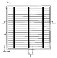
- FIG. 3 is a cross-sectional view showing an XZ cross section at a position indicated by a one-dot chain line III-III in FIG.
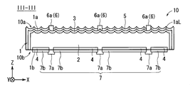
- FIG. 3 is a cross-sectional view showing an XZ cross section at a position indicated by a one-dot chain line III-III in FIG.
- It is an exploded view showing typically a section of a solar cell module concerning one embodiment.
- It is a top view which shows typically the external appearance of the solar cell module which concerns on one Embodiment.
- It is a flowchart which shows the manufacture flow of the solar cell element which concerns on one Embodiment.
- 1 to 5 are provided with a right-handed XYZ coordinate system in which the extending direction of the first output extraction electrode 6a (the upward direction in the drawing of FIG. 1) is the Y direction.
- ⁇ (1) Solar cell element> 1 to 3 are diagrams showing a solar cell element 10 according to an embodiment.
- the solar cell element 10 has a first main surface 10 a and a second main surface 10 b.
- the first major surface 10a is a surface that receives incident light (also referred to as a light receiving surface).
- the 2nd main surface 10b is a surface (it is also called a non-light-receiving surface) located in the solar cell element 10 on the opposite side to the 1st main surface 10a.
- the first main surface 10 a is drawn as the + Z side upper surface of the solar cell element 10
- the second main surface 10 b is drawn as the ⁇ Z side lower surface of the solar cell element 10.
- the solar cell element 10 includes a plate-like semiconductor substrate 1.
- the semiconductor substrate 1 includes a first semiconductor layer 2 and a second semiconductor layer 3.
- the first semiconductor layer 2 is a first conductivity type semiconductor layer.
- the second semiconductor layer 3 is a second conductivity type semiconductor layer having a conductivity type opposite to the first conductivity type.
- the second semiconductor layer 3 is disposed at least on the first main surface 10 a side of the first semiconductor layer 2.
- the solar cell element 10 includes a first electrode 6 electrically connected to the second semiconductor layer 3 disposed on the first main surface 10a side.
- the solar cell element 10 includes a semiconductor substrate 1, a third semiconductor layer 4, an antireflection layer 5, a first electrode 6, and a second electrode 7.
- the semiconductor substrate 1 includes the first semiconductor layer 2 and the second semiconductor layer 3 provided on the first main surface 10a side of the first semiconductor layer 2.
- the first semiconductor layer 2 a plate-like semiconductor having the first conductivity type can be adopted.
- the first conductivity type may be a p-type, for example.
- crystalline silicon such as single crystal silicon and polycrystalline silicon can be adopted.
- the thickness of the first semiconductor layer 2 may be, for example, 250 ⁇ m or less, and may be 150 ⁇ m or less.
- the shape of the first semiconductor layer 2 is not particularly limited, but for example, the first semiconductor layer 2 can be easily manufactured if the first semiconductor layer 2 has a quadrangular shape in plan view.
- a plate-like substrate of crystalline silicon exhibiting p-type conductivity also referred to as a crystalline silicon substrate
- the first semiconductor layer 2 can exhibit a p-type conductivity type.
- the second semiconductor layer 3 is a semiconductor layer exhibiting a second conductivity type opposite to that of the first semiconductor layer 2.
- the second semiconductor layer 3 is disposed at least on the first main surface 10 a side of the first semiconductor layer 2.
- the first semiconductor layer 2 and the second semiconductor layer 3 form a pn junction region.
- the second semiconductor layer 3 may be formed so as to exhibit n-type conductivity.
- the second semiconductor layer is formed in the surface layer of the crystalline silicon substrate. 3 is formed.
- a portion of the crystalline silicon substrate other than the second semiconductor layer 3 can be the first semiconductor layer 2.
- the second semiconductor layer 3 may be formed so as to exhibit p-type conductivity.
- an uneven portion 1aL is arranged on the first main surface 1a side of the semiconductor substrate 1.
- the height of the convex portion in the uneven portion 1aL may be, for example, 0.1 ⁇ m or more and 10 ⁇ m or less, and the width of the convex portion may be, for example, about 1 ⁇ m or more and 20 ⁇ m or less.
- grooved part 1aL should just be a substantially spherical shape, for example.
- the height of the convex portion referred to here is based on a plane (also referred to as a reference plane) passing through the bottom surface of the concave portion and parallel to the second main surface 10b, and from the reference plane in the normal direction of the reference plane. It means the distance to the top surface of the convex part.
- the width of the convex part means the distance between the top surfaces of an adjacent convex part in the direction parallel to the said reference plane.
- the antireflection layer 5 is a film for improving the efficiency of light absorption in the solar cell element 10.
- the antireflection layer 5 is disposed on the first main surface 1 a side of the semiconductor substrate 1.
- a material of the antireflection layer 5 for example, silicon nitride, titanium oxide, silicon oxide, magnesium oxide, indium tin oxide, tin oxide or zinc oxide is employed.
- the thickness of the antireflection layer 5 may be appropriately set according to the materials of the semiconductor substrate 1 and the antireflection layer 5. Thereby, in the solar cell element 10, it is possible to realize a condition in which light is not easily reflected by irradiation with various light.
- the refractive index of the antireflection layer 5 may be, for example, about 1.8 or more and 2.3 or less, and the thickness of the antireflection layer 5 is For example, it may be about 50 nm or more and 120 nm or less.
- the antireflection layer 5 functions as a passivation film, thereby realizing a passivation effect.
- the third semiconductor layer 4 is formed on the second main surface 1 b side of the semiconductor substrate 1.
- the third semiconductor layer 4 has the same conductivity type as the first semiconductor layer 2.
- the concentration of the dopant element in the third semiconductor layer 4 is higher than the concentration of the dopant element in the first semiconductor layer 2. That is, the third semiconductor layer 4 is formed by doping the semiconductor substrate 1 with a dopant element at a higher concentration than the dopant element doped into the semiconductor substrate 1 to form the first semiconductor layer 2.
- the third semiconductor layer 4 has a role of reducing carrier recombination in a region of the semiconductor substrate 1 on the second main surface 1b side. For this reason, the presence of the third semiconductor layer 4 reduces a decrease in conversion efficiency in the solar cell element 10.
- the third semiconductor layer 4 generates an internal electric field on the second main surface 1 b side of the semiconductor substrate 1.
- the third semiconductor is diffused by diffusing a dopant element such as boron or aluminum on the second main surface 1b side of the semiconductor substrate 1.
- a dopant element such as boron or aluminum on the second main surface 1b side of the semiconductor substrate 1.
- Layer 4 is formed.
- the concentration of the dopant element in the third semiconductor layer 4 may be, for example, about 1 ⁇ 10 18 atoms / cm 3 or more and about 5 ⁇ 10 21 atoms / cm 3 or less.
- the first electrode 6 is disposed on the first main surface 1 a side of the semiconductor substrate 1. As shown in FIG. 1, the first electrode 6 includes, for example, a plurality of first output extraction electrodes 6a extending in the Y direction and a large number of linear first current collecting electrodes 6b extending in the X direction. And are included. Here, at least a part of the first output extraction electrode 6a is electrically connected to the first current collecting electrode 6b by crossing the first current collecting electrode 6b.
- the width of the first collector electrode 6b in the short direction may be, for example, about 50 ⁇ m or more and about 200 ⁇ m or less.
- the width in the short direction of the first output extraction electrode 6a may be, for example, about 1.3 mm or more and 2.5 mm or less.
- the width in the short direction of the first current collecting electrode 6b may be smaller than the width in the short direction of the first output extraction electrode 6a.
- interval of the adjacent 1st current collection electrodes 6b among the some 1st current collection electrodes 6b should just be 1.5 mm or more and about 3 mm or less.
- the thickness of the 1st electrode 6 should just be about 10 micrometers or more and about 40 micrometers or less, for example.
- a conductive paste containing silver as a main component also referred to as a silver paste
- the first electrode 6 is formed.
- the second electrode 7 is disposed on the second main surface 1b side of the semiconductor substrate 1. As shown in FIG. 2, the second electrode 7 includes a second output extraction electrode 7a and a second current collecting electrode 7b.
- the thickness of the second output extraction electrode 7a may be, for example, about 10 ⁇ m or more and about 30 ⁇ m or less.
- the width of the second output extraction electrode 7a in the short direction may be, for example, not less than 1.3 mm and not more than 7 mm.
- the second output extraction electrode 7a is formed by the same material and manufacturing method as the first electrode 6. That is, the second output extraction electrode 7a is formed, for example, by baking after a silver paste is applied in a desired pattern on the second main surface 1b side of the semiconductor substrate 1 by screen printing or the like.
- the second current collecting electrode 7b may be formed on substantially the entire surface of the main surface on the second main surface 1b side of the semiconductor substrate 1 except for the region where the second output extraction electrode 7a is formed.
- the thickness of the 2nd current collection electrode 7b should just be 15 micrometers or more and about 50 micrometers or less.
- a conductive paste containing aluminum as a main component also referred to as an aluminum paste
- the solar cell module 20 includes one or more solar cell elements 10.
- the solar cell module 20 may include a plurality of solar cell elements 10 that are electrically connected.
- Such a solar cell module 20 is formed by connecting a plurality of solar cell elements 10 in series and in parallel, for example, when the electric output of a single solar cell element 10 is small.
- a practical electrical output can be taken out by combining a plurality of solar cell modules 20.
- the solar cell module 20 includes a plurality of solar cell elements 10 will be described.
- the solar cell module 20 is a laminate in which, for example, a transparent member 22, a front side filler 24, a plurality of solar cell elements 10, a wiring member 21, a back side filler 25, and a back surface protective material 23 are laminated.
- the transparent member 22 is a member for protecting the light receiving surface that receives sunlight in the solar cell module 20.
- the transparent member 22 may be, for example, a transparent flat plate member.
- the front side filler 24 and the back side filler 25 may be, for example, a transparent filler.
- the back surface protective material 23 is a member for protecting the solar cell module 20 from the back surface.
- EVA ethylene / vinyl acetate copolymer
- the back surface protective material 23 is a member for protecting the solar cell module 20 from the back surface.
- PET polyethylene terephthalate
- PVF polyvinyl fluoride resin
- the back surface protective material 23 may have a single layer structure or a laminated structure.
- the wiring member 21 is a member (also referred to as a connection member) that electrically connects the plurality of solar cell elements 10.
- the solar cell elements 10 adjacent to each other in the Y direction are the first electrode 6 of one solar cell element 10 and the second electrode of the other solar cell element 10. 7 is connected by a wiring member 21.
- the thickness of the wiring member 21 may be, for example, about 0.1 mm or more and about 0.2 mm or less.
- the width of the wiring member 21 may be about 2 mm.
- a member in which the entire surface of a copper foil is coated with solder is used as the wiring member 21.
- the solar cell module 20 may be provided with the frame 28 which hold
- the material of the frame body 28 for example, aluminum having both corrosion resistance and strength is employed.
- the solar cell element 10 included in the solar cell module 20 for example, due to the presence of the concavo-convex portion 1aL, the reflectance of light on the light receiving surface is reduced, and the light enters the solar cell element 10 inside. It is possible to capture efficiently. Moreover, in the solar cell element 10, high output characteristics are easily realized by reducing metal elements mixed in the semiconductor substrate 1 described later. Therefore, the solar cell module 20 excellent in output characteristics is realized.
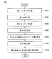
- FIG. 6 is a flowchart showing a manufacturing flow of the solar cell element 10 according to the embodiment.
- the solar cell element 10 is manufactured by sequentially performing steps S1 to S6.
- step S1 a step of preparing the semiconductor substrate 1 exhibiting the first conductivity type (also referred to as a substrate preparation step) is performed.
- the first conductivity type may be p-type, for example.
- step S2 the first main surface 1a of the semiconductor substrate 1 is subjected to an etching process using an acid aqueous solution, whereby a step of forming the uneven portion 1aL on the first main surface 1a (also referred to as an uneven portion forming step). Done.
- step S3 a process of forming a second semiconductor layer 3 of a second conductivity type opposite to the first conductivity type in a region on the first main surface 1a side of the semiconductor substrate 1 (also referred to as a semiconductor layer forming process). Is done.
- a portion of the semiconductor substrate 1 other than the second semiconductor layer 3 can be the first semiconductor layer 2.
- the semiconductor substrate 1 having the first semiconductor layer 2 exhibiting the p-type conductivity and the second semiconductor layer 3 exhibiting the n-type conductivity and having the uneven portion 1aL is formed.
- step S4 a step of forming the antireflection layer 5 on the first main surface 1a of the semiconductor substrate 1, that is, the second semiconductor layer 3 (also referred to as an antireflection layer forming step) is performed.
- step S5 a step of forming the third semiconductor layer 4 by diffusing the first conductivity type dopant element in a high concentration in the region on the second main surface 1b side of the semiconductor substrate 1 (a high concentration diffusion layer). Also referred to as a forming step).
- step S ⁇ b> 6 the first electrode 6 is formed on the second conductive type second semiconductor layer 3 in the semiconductor substrate 1, and the second side opposite to the first main surface 1 a in the semiconductor substrate 1 is formed.
- a step of forming second electrode 7 on main surface 1b (also referred to as an electrode forming step) is performed.
- the semiconductor substrate 1 is a single crystal silicon substrate
- the semiconductor substrate 1 is formed by, for example, a pulling method or the like.
- the semiconductor substrate 1 is a polycrystalline silicon substrate
- the semiconductor substrate 1 is formed by, for example, a casting method. In the following, an example in which a p-type polycrystalline silicon substrate is used as the semiconductor substrate 1 will be described.
- FIG. 7 is a flowchart showing a processing flow according to one aspect of the substrate preparation process.
- the semiconductor substrate 1 is prepared by sequentially performing the processes of steps S11 to S13.
- step S11 for example, an ingot of polycrystalline silicon as a semiconductor material is manufactured by a casting method.
- step S12 the ingot produced in step S11 is sliced to a thickness of 250 ⁇ m or less, for example.
- the ingot is sliced by a fixed abrasive type wire saw apparatus using a wire (also referred to as an abrasive fixed wire) to which abrasive grains are fixed in advance.
- the semiconductor substrate 1 is formed.
- step S13 the semiconductor substrate 1 contaminated in step S12 is cleaned by cleaning with a cleaning liquid. Thereby, the semiconductor substrate 1 is prepared.
- the semiconductor substrate 1 prepared by the substrate preparation step has a layer having mechanical damage (also referred to as a mechanical damage layer) in the cut surface and the region in the vicinity thereof, which are generated by being thinly sliced.
- a layer having mechanical damage also referred to as a mechanical damage layer
- the cut surface of the semiconductor substrate 1 formed by the fixed abrasive type wire saw device is compared with the cut surface of the semiconductor substrate formed by the free abrasive type wire saw device.
- the electron microscope may be a scanning electron microscope (SEM), for example.
- the cut surface of the semiconductor substrate 1 formed by the fixed abrasive type wire saw device is compressed to about 200 MPa or more and about 500 MPa or less. There is stress.
- the compressive stress in the cut surface of the semiconductor substrate formed with the loose abrasive type wire saw device is 200 MPa or less. That is, it is presumed that the use of the fixed abrasive type wire saw device provides the semiconductor substrate 1 with a small mechanical damage layer and a small release of residual stress due to the occurrence of microcracks or the like.
- the surface of the semiconductor substrate 1 may be subjected to a very small amount of etching process using an aqueous solution such as NaOH, KOH, hydrofluoric acid, or hydrofluoric acid.
- an aqueous solution such as NaOH, KOH, hydrofluoric acid, or hydrofluoric acid.
- Uneven portion forming step> As a method for forming the uneven portion 1aL, a wet etching process using an alkaline aqueous solution such as NaOH and an acid aqueous solution such as hydrofluoric acid, or a dry etching process using RIE (Reactive Ion Etching) or the like is adopted.
- RIE Reactive Ion Etching
- an etching treatment with an acid aqueous solution containing hydrofluoric acid and nitric acid is performed on the first main surface 1a.
- grooved part 1aL is formed in the 1st main surface 1a.
- at least one of an etching process using an acid aqueous solution containing hydrofluoric acid and hydrochloric acid (also referred to as a mixed acid aqueous solution) and an etching process using a hydrofluoric acid aqueous solution and a hydrochloric acid aqueous solution is performed on the first main surface 1a. Applied.
- a step in which the semiconductor substrate 1 is washed with water may be performed after the first treatment step and before the second treatment step.
- a water washing process in which the semiconductor substrate 1 is washed with water may be performed.
- these water washing steps may not be performed.
- FIG. 8 is a flowchart showing an example of the processing flow of the first aspect of the uneven portion forming step.
- the concavo-convex portion 1aL is formed on the first main surface 1a of the semiconductor substrate 1 by sequentially performing the processes of steps S21 to S25.
- step S21 for example, a first processing step is performed.
- the semiconductor substrate 1 is immersed in an acid aqueous solution containing hydrofluoric acid and nitric acid. Thereby, the uneven part 1aL is formed on the first main surface 1a of the semiconductor substrate 1.
- step S22 a water washing process in which the semiconductor substrate 1 is washed with water is performed.
- a cassette holding one or more semiconductor substrates 1 may be immersed in water placed in a washing treatment tank.
- the time for which the cassette is immersed in water may be, for example, about 5 seconds or more and about 60 seconds or less.
- the temperature of water should just be about 15 degreeC or more and 40 degrees C or less, for example.
- the semiconductor substrate 1 may be washed with water by pouring water onto the semiconductor substrate 1 using a device such as a shower. Thereby, mixing of the acid aqueous solution to the process in the next process of the water washing process is reduced.
- step S23 the second processing step is performed. Thereby, the stain film formed on the surface of the semiconductor substrate 1 is removed.
- the semiconductor substrate 1 may be immersed in an alkaline aqueous solution.
- an aqueous solution containing at least one of sodium hydroxide, potassium hydroxide, ammonium hydroxide and sodium carbonate is employed as the alkaline aqueous solution.
- a cassette holding one or more semiconductor substrates 1 may be immersed in an aqueous ammonium hydroxide solution placed in a treatment tank.
- the mass concentration of ammonium hydroxide in the aqueous ammonium hydroxide solution may be, for example, 0.005% or more and 5% or less.
- the time for which the cassette is immersed in the aqueous ammonium hydroxide solution may be, for example, about 5 seconds or more and about 200 seconds or less.
- the temperature of the ammonium hydroxide aqueous solution should just be about 10 degreeC or more and about 40 degrees C or less, for example.
- step S24 a water washing process is performed in which the semiconductor substrate 1 is washed with water.
- the process similar to the water washing process in step S22 should just be performed. Thereby, mixing of alkaline aqueous solution to the process in the next process of the water washing process is reduced.
- step S25 a third processing step is performed.
- the semiconductor substrate 1 is immersed in a mixed acid aqueous solution containing hydrofluoric acid and hydrochloric acid.
- the alkaline aqueous solution adhering to the semiconductor substrate 1 is neutralized by the mixed acid aqueous solution or the like, and the oxide film formed on the surface of the semiconductor substrate 1 is removed.
- sodium ions, potassium ions, and the like attached to the vicinity of the surface of the semiconductor substrate 1 in the second processing step in step S23 are removed by hydrochloric acid.
- a water washing step and a drying step may be employed.
- the immersion of the semiconductor substrate 1 in an aqueous hydrofluoric acid solution and the immersion of the semiconductor substrate 1 in an aqueous hydrochloric acid solution may be performed in order.
- treatment with steam containing hydrofluoric acid and hydrochloric acid may be performed.
- the steam containing hydrofluoric acid and hydrochloric acid is generated, for example, by heating a mixed acid aqueous solution containing hydrofluoric acid and hydrochloric acid.
- the vapor containing hydrofluoric acid and hydrochloric acid is also generated by other methods such as carrier gas being blown into the mixed acid aqueous solution containing hydrofluoric acid and hydrochloric acid and vented.
- treatment with steam containing hydrofluoric acid and treatment with steam containing hydrochloric acid may be performed in order. That is, in the third treatment step, it is only necessary to perform etching treatment with hydrofluoric acid and hydrochloric acid on the first main surface 1a.
- the concavo-convex portion may also be formed on the second main surface 1b side of the semiconductor substrate 1.
- a dry etching process using RIE or the like is performed.
- an etching residue is attached to the first main surface 1a of the semiconductor substrate 1 to perform etching (also referred to as a residue utilizing etching step), and the first main surface 1a.
- Steps for removing etching residues are sequentially performed.
- an etching process using hydrofluoric acid and hydrochloric acid is performed on the first main surface 1a. Thereby, an etching residue is removed from the 1st main surface 1a.
- FIG. 9 is a flowchart showing an example of the processing flow of the second aspect of the uneven portion forming step.
- step S2 instead of step S2 in which the processes in steps S21 to S25 shown in FIG. 8 are performed, step S2A in which the processes in steps S21A to S22A are sequentially performed is performed.
- the uneven part 1aL can be formed on the first main surface 1a of the semiconductor substrate 1.
- step S21A an etching process using residue is performed.
- a chlorine-based gas, a fluorine-based gas, and an oxygen gas are used as an etching gas, and the etching gas is turned into plasma, whereby the first main surface 1a is etched.
- the constituent components are separated from the first main surface 1a of the semiconductor substrate 1 by the corrosive action, but a part of the constituent components are not completely detached from the first main surface 1a, and the semiconductor substrate The first main surface 1a may remain attached to the first main surface 1a. Further, a part of the constituent components once detached from the first main surface 1a can be adsorbed again on the first main surface 1a.
- the constituent components remaining and adsorbed again on the first main surface 1a become etching residues. That is, in this etching process, an etching residue mainly composed of the material of the semiconductor substrate 1 is intentionally left and reattached to the first main surface 1a of the semiconductor substrate 1, and the etching residue is used as a mask. Then, the etching residue is used as a mask in the etching process, whereby the first main surface 1a of the semiconductor substrate 1 is roughened.
- step S22A a residue removal process is performed.
- the first major surface 1a of the semiconductor substrate 1 is treated with a mixed acid aqueous solution containing hydrofluoric acid and hydrochloric acid, whereby the etching residue is removed from the first major surface 1a.
- a mixed acid aqueous solution containing hydrofluoric acid and hydrochloric acid for example, a dilute hydrofluoric acid aqueous solution containing hydrochloric acid having a mass concentration of hydrochloric acid of 2% or more and 20% or less is employed.
- a cassette holding one or more semiconductor substrates 1 may be immersed in a dilute hydrofluoric acid aqueous solution containing hydrochloric acid placed in a treatment tank.
- the mass concentration of hydrochloric acid in the dilute hydrofluoric acid aqueous solution containing hydrochloric acid may be an arbitrary mass concentration set in advance.
- the time for which the cassette is immersed in the dilute hydrofluoric acid aqueous solution containing hydrochloric acid may be, for example, about 5 seconds or longer and within about 120 seconds.
- the temperature of the dilute hydrofluoric acid aqueous solution containing hydrochloric acid may be, for example, about 10 ° C. or more and about 60 ° C. or less.
- a water washing step and a drying step may be employed.
- the immersion of the semiconductor substrate 1 in a hydrofluoric acid aqueous solution and the immersion of the semiconductor substrate 1 in a hydrochloric acid aqueous solution may be sequentially performed.
- treatment with steam containing hydrofluoric acid and hydrochloric acid may be performed.
- the steam containing hydrofluoric acid and hydrochloric acid is generated, for example, by heating a mixed acid aqueous solution containing hydrofluoric acid and hydrochloric acid.
- the vapor containing hydrofluoric acid and hydrochloric acid is also generated by other methods such as carrier gas being blown into the mixed acid aqueous solution containing hydrofluoric acid and hydrochloric acid and vented.
- treatment with steam containing hydrofluoric acid and treatment with steam containing hydrochloric acid may be sequentially performed. That is, in the residue removal step, the first main surface 1a may be etched with hydrofluoric acid and hydrochloric acid.
- the uneven portion 1aL formed by RIE becomes a fine uneven portion than the uneven portion 1aL formed by using a wet etching process. For this reason, the water repellency tends to deteriorate in the portion of the first main surface 1a where the uneven portion 1aL is formed.
- the natural oxide film formed on the first main surface 1a by the contact with the atmosphere after the residue-use etching process in step S21A is effectively treated with, for example, a mixed acid aqueous solution containing hydrochloric acid. Removed. Thereby, the water repellency of the first main surface 1a of the semiconductor substrate 1 is improved. As a result, the first main surface 1a after the treatment with the liquid can be easily dried, and the generation of the watermark on the first main surface 1a is reduced.
- the first main surface 1a is subjected to a first etching process using an acid aqueous solution (also referred to as a first acid aqueous solution) containing hydrofluoric acid, nitric acid and sulfuric acid.
- the first main surface 1a is subjected to a second etching process using an acid aqueous solution (also referred to as a second acid aqueous solution) containing hydrofluoric acid and nitric acid and substantially free of sulfuric acid.
- substantially free of sulfuric acid means that a very small amount of sulfuric acid is allowed to be contained.
- a first water washing step in which the semiconductor substrate 1 is washed after the first etching treatment step and before the second etching treatment step may be performed.
- the 2nd water washing process by which the semiconductor substrate 1 is washed with water may be performed after a 2nd etching process process.
- any one of these 1st and 2nd water washing processes may be performed, and both do not need to be performed.
- the stain film may be removed by immersing the semiconductor substrate 1 in an alkaline aqueous solution.
- the 3rd water washing process by which the semiconductor substrate 1 is washed with water after the process by aqueous alkali solution may be performed.
- FIG. 10 is a flowchart showing an example of the processing flow of the third aspect of the uneven portion forming step.
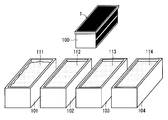
- FIG. 11 is a figure for demonstrating the 3rd aspect of an uneven
- step S2B instead of step S2 in which the processes in steps S21 to S25 shown in FIG. 8 are performed, step S2B in which the processes in steps S21B to S27B are sequentially performed is performed.
- the uneven part 1aL is formed on the first main surface 1a of the semiconductor substrate 1.
- the semiconductor substrate 1 is used which has few mechanical damage layers and little release of residual stress due to generation of microcracks or the like.
- step S ⁇ b> 21 ⁇ / b> B the first etching process using the first acid aqueous solution 111 is performed on the first main surface 1 a of the semiconductor substrate 1.
- a cassette 100 holding about tens to hundreds of semiconductor substrates 1 is immersed in a first acid aqueous solution 111 placed in a first treatment tank 101.
- the semiconductor substrate 1 may be immersed in the first acid aqueous solution 111 such that the first main surface 1a of the semiconductor substrate 1 and the liquid surface of the first acid aqueous solution 111 have a substantially vertical relationship.
- the method of immersing the semiconductor substrate 1 in the first acid aqueous solution 111 is not limited to the method of immersing the cassette 100 in the first acid aqueous solution 111.
- the semiconductor substrate 1, and the like. are appropriately selected.
- the first acid aqueous solution 111 is, for example, a mixture of a hydrofluoric acid aqueous solution having a hydrofluoric acid mass concentration of 46%, a nitric acid aqueous solution having a nitric acid mass concentration of 60%, and a sulfuric acid aqueous solution having a mass concentration of sulfuric acid of 95%. If it is good.
- the ratio of the volume of the hydrofluoric acid aqueous solution having a mass concentration of hydrofluoric acid of 46%, the volume of the nitric acid aqueous solution having a mass concentration of 60% nitric acid, and the volume of the sulfuric acid aqueous solution having a mass concentration of sulfuric acid of 95% to be mixed.
- the temperature of the first acid aqueous solution 111 may be, for example, about 15 ° C. or more and about 40 ° C. or less.
- the time for which the semiconductor substrate 1 is immersed in the first acid aqueous solution 111 may be, for example, about 10 seconds or more and about 180 seconds or less.
- the first acid aqueous solution 111 may contain other acid different from hydrofluoric acid, nitric acid, and sulfuric acid.
- the etching speed in the first etching process may be controlled by adding acetic acid to the first acid aqueous solution 111.
- the first acid aqueous solution 111 is used, so that the surface of the silicon substrate as the semiconductor substrate 1 is oxidized by nitric acid to form silicon oxide. At this time, bubbles such as a nitrogen oxide gas and a nitrogen oxide hydrogen gas are generated. The generated silicon oxide is etched with hydrofluoric acid.
- the chemical formula of the main reaction in the first etching process is as follows.
- HNO 2 gas bubbles are generated when HNO in a substance (also referred to as a reaction product) generated by the reaction further reacts with water.
- a substance also referred to as a reaction product
- the viscosity of the first acid aqueous solution 111 is increased by the inclusion of sulfuric acid.
- the etching process of the semiconductor substrate 1 is slower in the region in contact with the bubbles than in the region not in contact with the bubbles, so One main surface 1a is suitably formed.
- the HNO 2 gas bubbles are easily held locally between the semiconductor substrates 1 adjacent in the cassette 100.
- the interval between adjacent semiconductor substrates 1 is not less than 3 mm and not more than 5 mm, bubbles are easily held between adjacent semiconductor substrates 1.
- rate of the etching process of the semiconductor substrate 1 becomes slow.
- a concavo-convex portion is further suitably formed on the first main surface 1 a of the semiconductor substrate 1.
- the etching process can preferentially proceed even at a crystal defect portion in the damaged layer on the surface of the semiconductor substrate 1. For this reason, on the surface of the semiconductor substrate 1, the damaged layer is used as a starting point to form a recess, and the etching process can proceed. As a result, the shape of the concave portion on the surface of the semiconductor substrate 1 is increased, and the concave and convex portion is suitably formed.
- the concavo-convex portion formed on the first main surface 1a in the first etching step has a larger number of regions where the convex portions are flat than the final concavo-convex portion 1aL of the semiconductor substrate 1. That is, in the concavo-convex portion formed by the first acid aqueous solution 111, the top surface of the bulge is wider than the final concavo-convex portion 1 aL of the semiconductor substrate 1.
- the amount of etching of the semiconductor substrate 1 in the first etching step (also referred to as etching amount) is, for example, that the amount of change in the weight of the semiconductor substrate 1 before and after the etching process is converted into the thickness of the semiconductor substrate 1. Is calculated by The etching amount may be, for example, a thickness of 0.1 ⁇ m or more and 20 ⁇ m or less on one surface of the semiconductor substrate 1.
- step S22B a first water washing step in which the semiconductor substrate 1 is washed with water is performed. Thereby, mixing of the 1st acid aqueous solution 111 to the 2nd acid aqueous solution 113 used in the 2nd etching process of step S23B is reduced. As a result, the etching rate in the second etching process is maintained.
- the cassette 100 holding about several tens to hundreds of semiconductor substrates 1 is immersed in the water 112 placed in the first washing tank 102.
- the time for which the cassette is immersed in the water 112 may be, for example, about 5 seconds or more and about 60 seconds or less.
- the temperature of the water 112 should just be 15 degreeC or more and about 40 degreeC or less, for example.
- the semiconductor substrate 1 may be washed with water by pouring water onto the semiconductor substrate 1 using a device such as a shower. Thereby, mixing of the 1st acid aqueous solution 111 to the process in the next process of a 1st water washing process is reduced.
- step S23B a second etching process using the second acid aqueous solution 113 is performed on the first main surface 1a of the semiconductor substrate 1.
- a cassette 100 holding about several tens to hundreds of semiconductor substrates 1 is immersed in a second acid aqueous solution 113 placed in a second treatment tank 103.
- the etching process with the second acid aqueous solution 113 is performed on the first main surface 1a of the semiconductor substrate 1 that has been subjected to the etching process with the first acid aqueous solution 111.
- the semiconductor substrate 1 may be immersed in the second acid aqueous solution 113 so that the first main surface 1a of the semiconductor substrate 1 and the liquid surface of the second acid aqueous solution 113 have a substantially vertical relationship.
- the second acid aqueous solution 113 may be, for example, a mixture of a hydrofluoric acid aqueous solution having a hydrofluoric acid mass concentration of 46%, a nitric acid aqueous solution having a mass concentration of nitric acid of 60%, and water.
- the ratio of the volume of the hydrofluoric acid aqueous solution having a mass concentration of 46% hydrofluoric acid and the volume of the aqueous nitric acid having a mass concentration of nitric acid of 60% and the volume of water mixed at this time is, for example, 2 to 6:12. : 5 to 20 is sufficient.
- the temperature of the second acid aqueous solution 113 may be, for example, about 5 ° C.
- the time for which the semiconductor substrate 1 is immersed in the second acid aqueous solution 113 may be, for example, about 60 seconds or more and about 180 seconds or less.
- the second acid aqueous solution 113 may contain other acid different from hydrofluoric acid, nitric acid, and sulfuric acid.
- the rate of etching in the second etching process may be controlled by adding acetic acid to the second acid aqueous solution 113.
- the second acid aqueous solution 113 is used, so that the etching process proceeds on the first main surface 1a based on the uneven portion formed by the first acid aqueous solution 111.
- grooved part can reduce.
- the concavo-convex portion 1aL where light reflection is suitably reduced is formed.
- the chemical formula of the main reaction in the second etching step is as follows.
- the amount (etching amount) by which the semiconductor substrate 1 is etched in the second etching step is calculated by converting the amount of change in the weight of the semiconductor substrate 1 before and after the etching process into the thickness of the semiconductor substrate 1. .
- the etching amount may be, for example, a thickness of 1 ⁇ m or more and 5 ⁇ m or less on one surface of the semiconductor substrate 1.
- the uneven part 1aL is formed on the first main surface 1a side of the semiconductor substrate 1.
- the height of the convex portion in the uneven portion 1aL may be, for example, 0.1 ⁇ m or more and 10 ⁇ m or less, and the width of the convex portion may be, for example, about 1 ⁇ m or more and 20 ⁇ m or less.
- grooved part 1aL should just be a substantially spherical shape, for example.
- the temperature T2 of the second acid aqueous solution 113 in the second etching step may be lower than the temperature T1 of the first acid aqueous solution 111 in the first etching step. That is, the second etching process using the second acid aqueous solution 113 may be performed on the first main surface 1a of the semiconductor substrate 1 while the relationship of T1> T2 is satisfied. Thereby, the reaction between the second acid aqueous solution 113 and the semiconductor substrate 1 is reduced, and the portion where the bond between silicon atoms is weak is preferentially etched. As a result, the concavo-convex portion 1aL in which the reflection of light is further reduced is formed. In this case, the temperature of the 2nd acid aqueous solution 113 should just be set to 5 degreeC or more and 12 degrees C or less, for example.
- the ratio of the mass of nitric acid to the mass of hydrofluoric acid in the second acid aqueous solution 113 may be larger than the ratio of the mass of nitric acid to the mass of hydrofluoric acid in the first acid aqueous solution 111.
- the value obtained by dividing the mass of nitric acid by the mass of hydrofluoric acid may be larger in the second acid aqueous solution 113 than in the first acid aqueous solution 111.
- the second etching process is performed on the semiconductor substrate 1 by the second acid aqueous solution 113 in which the ratio R2 of the mass of nitric acid to the mass of hydrofluoric acid is larger than the ratio R1 of the mass of nitric acid to the mass of hydrofluoric acid in the first acid aqueous solution 111.
- the first main surface 1a may be provided.
- the ratio R1 may be a value obtained by dividing the mass of nitric acid by the mass of hydrofluoric acid for the first acid aqueous solution 111.
- the ratio R2 may be a value obtained by dividing the mass of nitric acid by the mass of hydrofluoric acid for the second acid aqueous solution 113.
- the ratio R1 and the ratio R2 may be, for example, the ratio of the volume of the nitric acid aqueous solution to the volume of the hydrofluoric acid aqueous solution for the hydrofluoric acid aqueous solution and the nitric acid aqueous solution to be mixed. That is, a value obtained by dividing the volume of the nitric acid aqueous solution by the volume of the hydrofluoric acid aqueous solution may be used. In this case, for example, a hydrofluoric acid aqueous solution having a mass concentration of hydrofluoric acid of 46% and a nitric acid aqueous solution having a mass concentration of nitric acid of 60% may be used.
- step S24B a second water washing process is performed in which the semiconductor substrate 1 is washed with water. Thereby, mixing of the 2nd acid aqueous solution 113 to the alkaline aqueous solution used in the process of step S25B is reduced.
- a cassette 100 holding several tens to hundreds of semiconductor substrates 1 is filled with water 114 placed in the second water washing tank 104. Soaked in.
- the time for which the cassette is immersed in the water 114 may be, for example, about 5 seconds or more and about 60 seconds or less.
- the temperature of water 114 should just be 15 degreeC or more and about 40 degrees C or less, for example.
- the semiconductor substrate 1 may be washed with water by pouring water onto the semiconductor substrate 1 using a device such as a shower. Thereby, mixing of the 2nd acid aqueous solution 113 to the process in the next process of a 2nd water washing process is reduced.
- the semiconductor substrate 1 may be rinsed for a longer time than the time in which the semiconductor substrate 1 is washed in the first water washing step. That is, the washing time T4 in the second washing step may be longer than the washing time T3 in the first washing step. In this case, excessive growth of the stain film in the first water washing step is reduced. As a result, in the second etching step, a decrease in the etching rate due to the stain film is reduced.
- step S25B the stain film formed on the surface of the semiconductor substrate 1 is removed by treating the semiconductor substrate 1 with an alkaline aqueous solution.
- the semiconductor substrate 1 may be immersed in an alkaline aqueous solution.
- an aqueous solution containing at least one of sodium hydroxide, potassium hydroxide, ammonium hydroxide and sodium carbonate is employed as the alkaline aqueous solution.
- a cassette holding one or more semiconductor substrates 1 may be immersed in an aqueous ammonium hydroxide solution placed in a treatment tank.
- the mass concentration of ammonium hydroxide in the aqueous ammonium hydroxide solution may be, for example, 0.005% or more and 5% or less.
- the time for which the cassette is immersed in the aqueous ammonium hydroxide solution may be, for example, about 5 seconds or more and about 200 seconds or less.
- the temperature of the ammonium hydroxide aqueous solution should just be about 10 degreeC or more and about 40 degrees C or less, for example.
- step S26B a third water washing step in which the semiconductor substrate 1 is washed with water is performed. Thereby, mixing of alkaline aqueous solution to the process in the next process of a 3rd water washing process is reduced.
- the cassette 100 holding about several tens to hundreds of semiconductor substrates 1 is immersed in water placed in a water washing tank.
- the time for which the cassette is immersed in water may be, for example, about 5 seconds or more and about 60 seconds or less.
- the temperature of water should just be about 15 degreeC or more and 40 degrees C or less, for example.
- the semiconductor substrate 1 may be washed with water by pouring water onto the semiconductor substrate 1 using a device such as a shower. Thereby, mixing of alkaline aqueous solution to the process in the next process of a 3rd water washing process is reduced.
- step S27B the surface of the semiconductor substrate 1 is treated with an acid aqueous solution or the like.
- the alkaline aqueous solution adhering to the semiconductor substrate 1 is neutralized, and the oxide film formed on the surface of the semiconductor substrate 1 is removed.
- the cassette 100 holding about several tens to hundreds of semiconductor substrates 1 is a dilute hydrofluoric acid aqueous solution in which the mass concentration of hydrofluoric acid in the treatment tank is 0.1% or more and 25% or less. Soaked in.
- the temperature of dilute hydrofluoric acid aqueous solution should just be 10 degreeC or more and 40 degrees C or less, for example.
- the etching process by a hydrofluoric acid and hydrochloric acid may be performed similarly to a 3rd process process.
- a water washing step and a drying step may be employed.
- the semiconductor substrate 1 is immersed in the first acid aqueous solution 111 containing hydrofluoric acid, nitric acid, and sulfuric acid, and then contains hydrofluoric acid, nitric acid, and sulfuric acid.
- the concavo-convex portion 1aL is formed by being immersed in the second acid aqueous solution 113 which is not substantially contained.
- a suitable uneven portion 1aL is formed on the first main surface 1a of the semiconductor substrate 1.
- the width of the convex portion is larger in the concave-convex portion 1aL than the concave-convex portion formed by the etching process using only the first acid aqueous solution 111. That is, the concavo-convex portion 1aL where light reflection is suitably reduced is formed. And the presence of such an uneven portion 1aL reduces the reflectance of light on the light receiving surface, and the light is efficiently taken into the solar cell element 10.
- the etching process time until a desired etching amount is obtained can be increased. For this reason, in order to reduce the decrease in the etching process speed, for example, a new solution of the first acid aqueous solution 111 is usually added to the processing tank. However, when the number of semiconductor substrates 1 to be etched by the first acid aqueous solution 111 is increased, even if a new solution of the first acid aqueous solution 111 is added to the processing tank, the etching process speed is greatly reduced, which is preferable. There is a possibility that the uneven portion 1aL is not formed.
- the two-step etching process by the 1st etching process using the 1st acid aqueous solution 111 and the 2nd etching process using the 2nd acid aqueous solution 113 is carried out. Done. For this reason, the time for the etching process using the first acid aqueous solution 111 can be shortened. Thereby, even if the number of semiconductor substrates 1 subjected to the etching process using the first acid aqueous solution 111 is increased, a decrease in the etching process speed in the first etching process is reduced. As a result, the concavo-convex portion 1aL where light reflection is suitably reduced is formed.
- the concavo-convex portion may also be formed on the second main surface 1b side of the semiconductor substrate 1.
- the semiconductor layer forming step for example, the second semiconductor layer 3 is formed by using a thermal diffusion method.
- a thermal diffusion method for example, a specific aspect of the semiconductor formation process will be described.
- a step of forming a laminated portion of the second semiconductor layer 3 and the glass layer on the first main surface 1a side of the semiconductor substrate 1 (also referred to as a laminated portion forming step), and removing the glass layer Processes to be performed (also referred to as glass layer removal process) are performed in order.
- the laminated portion forming step for example, a second semiconductor layer 3 and a glass layer disposed on the second semiconductor layer 3 in a region on the first main surface 1a side of the semiconductor substrate 1 by a thermal diffusion method.
- a laminated portion in which is laminated is formed.
- the glass layer contains an element that becomes a dopant of the second conductivity type.
- the second semiconductor layer 3 and the glass layer are laminated not only in the region on the first main surface 1a side of the semiconductor substrate 1 but also in the region on the second main surface 1b side of the semiconductor substrate 1.
- a laminated portion may be formed.
- the glass layer removal step the glass layer using hydrofluoric acid and hydrochloric acid is removed.
- the laminated part containing the 2nd semiconductor layer 3 and a glass layer is formed in the 2nd main surface 1b side of the semiconductor substrate 1, it is after a laminated part formation process and before a glass layer removal process.
- the step of removing the laminated portion on the second main surface 1b side (also referred to as a laminated portion removing step) may be performed. Thereby, the glass layer and the second semiconductor layer 3 formed in the region on the second main surface 1b side are removed.
- the productivity of the solar cell element 10 is improved by a series of steps in which the glass layer removal step is subsequently performed after the stacked portion removal step.
- FIG. 12 is a flowchart illustrating a processing flow of one aspect of the semiconductor layer forming step.
- the second semiconductor layer 3 is formed on the first main surface 1a side of the semiconductor substrate 1 by sequentially performing the processes of steps S31 to S33.
- step S ⁇ b> 31 a laminated part forming process is performed in which the second semiconductor layer 3 and a glass layer disposed on the second semiconductor layer 3 are formed on the semiconductor substrate 1.
- step S ⁇ b> 32 a stacked portion removing process is performed in which the stacked portion including the second semiconductor layer 3 and the glass layer formed on the second main surface 1 b side of the semiconductor substrate 1 is removed.
- step S33 a glass layer removing process is performed in which the glass layer is removed using hydrofluoric acid and hydrochloric acid.
- the second conductive type second semiconductor layer 3 and the glass layer are formed in the region of the semiconductor substrate 1 on the first main surface 1a side.
- the second conductivity type may be n-type, for example.
- the second conductive type second semiconductor layer 3 and the glass layer may be formed in a region on the second main surface 1b side of the semiconductor substrate 1.
- the first semiconductor layer 3 As a method for forming the first semiconductor layer 3, for example, a coating thermal diffusion method in which thermal diffusion is performed after P 2 O 5 in a paste state is applied to the surface of the semiconductor substrate 1, and phosphorus oxychloride in a gas state A vapor phase thermal diffusion method using (POCl 3 ) as a diffusion source is employed.
- the thickness of the first semiconductor layer 3 formed at this time may be about 0.2 ⁇ m or more and about 2 ⁇ m or less.
- the thickness of the second semiconductor layer 3 is substantially equivalent to the depth at which the second semiconductor layer 3 is formed from the surface of the semiconductor substrate 1.
- the sheet resistance of the second semiconductor layer 3 may be 40 ⁇ / ⁇ or more and about 200 ⁇ / ⁇ .
- heat treatment in a temperature range of about 600 ° C. to 800 ° C. in an atmosphere containing a diffusion gas mainly containing POCl 3 or the like. May be applied to the semiconductor substrate 1.
- the heat treatment time may be about 5 minutes or more and about 30 minutes or less.
- a glass layer containing phosphorus as an element serving as an n-type conductivity dopant is formed in a region near the surface of the semiconductor substrate 1.
- the glass layer containing phosphorus can include a layer of primarily phosphorus glass.
- the semiconductor substrate 1 may be subjected to the next heat treatment in a high temperature range of 800 ° C.
- the heat treatment time may be about 10 minutes or more and about 40 minutes or less.
- Laminate removal process for example, an acid aqueous solution containing hydrofluoric acid and nitric acid (also referred to as a second mixed acid aqueous solution) is used, and the glass layer and the second layer formed on the second main surface 1b side of the semiconductor substrate 1 are used.
- the stacked portion including the semiconductor layer 3 is removed. Thereby, the first semiconductor layer 2 of the first conductivity type is exposed on the second main surface 1b of the semiconductor substrate 1.
- the first conductivity type may be p-type, for example.
- the second semiconductor layer 3 is formed by a vapor phase thermal diffusion method or the like in a state where a diffusion mask is arranged on the second main surface 1b of the semiconductor substrate 1 in advance.
- a diffusion mask is removed is also conceivable.
- the semiconductor substrate 1 may have the same structure as that after the laminated portion removing step. In this case, since the second semiconductor layer 3 and the glass layer are not formed on the second main surface 1b side of the semiconductor substrate 1, the stacked portion removing step is not necessary.
- FIG. 13 is a flowchart showing an example of the processing flow of the first aspect of the stacked portion removing step.
- the glass layer formed in the region on the second main surface 1b side of the semiconductor substrate 1 is obtained by sequentially performing the processes of steps S321 to S322.
- the stacked portion including the second semiconductor layer 3 is removed.
- step S321 an etching process using a second mixed acid aqueous solution containing hydrofluoric acid and nitric acid is performed. Specifically, an etching process in which the second mixed acid aqueous solution is used to remove the laminated portion including the glass layer and the second semiconductor layer 3 formed in the region on the second main surface 1b side of the semiconductor substrate 1. Is given. More specifically, for example, a glass layer formed on the second main surface 1b side of the semiconductor substrate 1 by immersing the second main surface 1b side of the semiconductor substrate 1 in a hydrofluoric acid aqueous solution as the second mixed acid aqueous solution, The second semiconductor layer 3 is removed.
- the glass layer and the second semiconductor layer 3 formed on the second main surface 1b side of the semiconductor substrate 1 in a state where the phosphor glass as the glass layer remains on the first main surface 1a side of the semiconductor substrate 1. Is removed.
- the second semiconductor layer 3 disposed on the first main surface 1a side of the semiconductor substrate 1 is removed due to the presence of phosphorous glass as the glass layer disposed on the first main surface 1a side of the semiconductor substrate 1. Further, damage given to the second semiconductor layer 3 is reduced.
- the second mixed acid aqueous solution may contain sulfuric acid in addition to hydrofluoric acid and nitric acid. That is, in the etching process of step S321, the second mixed acid aqueous solution containing hydrofluoric acid, nitric acid and sulfuric acid is used, and the glass layer and the second semiconductor layer formed in the region on the second main surface 1b side of the semiconductor substrate 1 are used. 3 may be subjected to an etching process in which the stacked portion including 3 is removed. In this case, the viscosity of the second mixed acid aqueous solution can increase. As a result, the second mixed acid aqueous solution scatters and the second mixed acid aqueous solution hardly adheres to the first main surface 1 a side of the semiconductor substrate 1. As a result, the removal of the second semiconductor layer 3 disposed on the first main surface 1a side of the semiconductor substrate 1 and the damage given to the second semiconductor layer 3 are further reduced.
- step S322 an alkaline aqueous solution is used, and a process of treating the second main surface 1b (also referred to as a first alkali treatment process) is performed.
- the semiconductor substrate 1 is immersed in an alkaline aqueous solution.
- an aqueous solution containing at least one of sodium hydroxide, potassium hydroxide, ammonium hydroxide and sodium carbonate is employed as the alkaline aqueous solution.
- the second main surface 1b side of the semiconductor substrate 1 may be immersed in an aqueous potassium hydroxide solution as an alkaline aqueous solution.
- the mass concentration of potassium hydroxide in the potassium hydroxide aqueous solution may be, for example, 1% or more and 20% or less.
- the time for which the cassette is immersed in the potassium hydroxide aqueous solution may be, for example, about 5 seconds or more and about 120 seconds or less.
- the temperature of potassium hydroxide aqueous solution should just be about 10 degreeC or more and about 40 degrees C or less, for example.
- step S321 the stain film formed on the second main surface 1b side of the semiconductor substrate 1 in the etching process of step S321 is removed by the first alkali treatment process. For this reason, a stain film may not be interposed between the second electrode 7 formed in the electrode forming process, which is a process subsequent to the semiconductor layer forming process, and the semiconductor substrate 1. As a result, the problem that the adhesion strength between the semiconductor substrate 1 and the second electrode 7 decreases due to the interposition of the stain film between the second electrode 7 and the semiconductor substrate 1 hardly occurs. Therefore, a decrease in output characteristics and a decrease in reliability of the solar cell element 10 are reduced.
- the water washing step in which the semiconductor substrate 1 is washed with water is performed after the etching step similar to that in the first aspect of the stacked portion removing step is performed.
- a first alkali treatment step similar to the first aspect of the stacked portion removing step may be performed.
- a water washing step in which the semiconductor substrate 1 is washed with water may be performed after the first alkali treatment step.
- FIG. 14 is a flowchart showing an example of the processing flow of the second aspect of the stacked portion removing step.
- step S32A in which the processes of steps S321A to S324A are sequentially performed is performed instead of step S32 in which the processes of steps S321 to S322 shown in FIG. 14 are performed.
- the laminated part including the glass layer and the second semiconductor layer 3 formed in the region on the second main surface 1b side of the semiconductor substrate 1 is removed.
- step S321A an etching process similar to that in step S321 in FIG. 13 is performed. That is, the second mixed acid aqueous solution containing hydrofluoric acid and nitric acid is used, and the stacked portion including the glass layer and the second semiconductor layer 3 formed in the region on the second main surface 1b side of the semiconductor substrate 1 is removed. Etching is performed.
- step S322A a water washing process in which the semiconductor substrate 1 is washed with water is performed.
- a cassette holding one or more semiconductor substrates 1 may be immersed in water placed in a washing treatment tank.
- the time for which the cassette is immersed in water may be, for example, about 5 seconds or more and about 60 seconds or less.
- the temperature of water should just be about 15 degreeC or more and 40 degrees C or less, for example.
- the semiconductor substrate 1 may be washed with water by pouring water onto the semiconductor substrate 1 using a device such as a shower. Thereby, mixing of the 2nd mixed acid aqueous solution to the process in the next process of an etching process is reduced.
- step S323A a first alkali treatment step similar to step S322 in FIG. 13 is performed. As a result, the stain film formed on the second main surface 1b side of the semiconductor substrate 1 in the etching step in step S321A is removed.
- step S324A a water washing process in which the semiconductor substrate 1 is washed with water is performed.
- a cassette holding one or more semiconductor substrates 1 may be immersed in water contained in a rinsing treatment tank.
- the time for which the cassette is immersed in water may be, for example, about 5 seconds or more and about 60 seconds or less.
- the temperature of water should just be about 15 degreeC or more and 40 degrees C or less, for example.
- the semiconductor substrate 1 may be washed with water by pouring water onto the semiconductor substrate 1 using a device such as a shower. Thereby, mixing of alkaline aqueous solution to the process in the process following a 1st alkali treatment process is reduced.
- glass layer removal step for example, an etching process using hydrofluoric acid and hydrochloric acid is performed.
- a wet etching process using an acid aqueous solution (also referred to as a first mixed acid aqueous solution) containing hydrofluoric acid and hydrochloric acid may be performed.
- an etching process using a vapor of hydrofluoric acid and a vapor of hydrochloric acid may be performed.
- the second conductivity type may be n-type, for example.
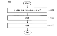
- FIG. 15 is a flowchart showing an example of the processing flow of the first aspect of the glass layer removal step.
- the glass layer formed on the first main surface 1a side of the semiconductor substrate 1 is removed by sequentially performing the processes of steps S331 to S333.
- step S331 an etching process using hydrofluoric acid and hydrochloric acid is performed. Thereby, the glass layer arranged on the first main surface 1a side of the semiconductor substrate 1 is removed.
- the glass layer may be phosphor glass or the like, for example.
- the first main surface 1a side of the semiconductor substrate 1 is disposed on the first main surface 1a side of the semiconductor substrate 1 by being treated with a first mixed acid aqueous solution containing hydrofluoric acid and hydrochloric acid.
- the glass layer is removed.
- a cassette holding about tens to hundreds of semiconductor substrates 1 is immersed in a first mixed acid aqueous solution placed in a processing tank.
- the semiconductor substrate 1 is immersed in the first mixed acid aqueous solution so that the first main surface 1a of the semiconductor substrate 1 and the liquid surface of the first mixed acid aqueous solution have a substantially vertical relationship.
- the method in which the semiconductor substrate 1 is immersed in the first mixed acid aqueous solution is not limited to the method in which the cassette is immersed in the first mixed acid aqueous solution.
- the shape of the semiconductor substrate 1, and the like. are appropriately selected.
- the solar cell element 10 having excellent output characteristics is realized as compared with the case where the glass layer is removed only with hydrofluoric acid.
- hydrochloric acid is contained in the first mixed acid aqueous solution used when the glass layer is removed, the removal efficiency of metal ions existing in the vicinity of the surface of the semiconductor substrate 1 due to the high reactivity of chloride ions. Can increase. That is, the removal efficiency of the metal element existing near the surface of the semiconductor substrate 1 can be increased.
- in 1st mixed acid aqueous solution low pH is implement
- the first mixed acid aqueous solution may be, for example, a mixture of a hydrofluoric acid aqueous solution having a hydrofluoric acid mass concentration of 46%, a hydrochloric acid aqueous solution having a mass concentration of hydrochloric acid of 35%, and water.
- the ratio of the volume of the hydrofluoric acid aqueous solution having a mass concentration of hydrofluoric acid of 46% and the volume of the aqueous hydrochloric acid solution having a mass concentration of hydrochloric acid of 35% and the volume of water mixed at this time is, for example, 1: 0.01. It may be up to 0.5: 5.
- the ratio between the mass concentration of hydrofluoric acid and the mass concentration of hydrochloric acid in the first mixed acid aqueous solution may be, for example, 2 to 100: 1.
- the mass concentration of hydrofluoric acid in the first mixed acid aqueous solution, may be not less than 2 times and not more than 100 times the mass concentration of hydrochloric acid.
- the temperature of the first mixed acid aqueous solution when the etching process is performed may be, for example, about 15 ° C. or more and about 40 ° C. or less.
- the time for which the semiconductor substrate 1 is immersed in the first mixed acid aqueous solution may be, for example, not less than 10 seconds and not more than 180 seconds.
- step S331 instead of performing the etching process using the first mixed acid aqueous solution on the first main surface 1a side of the semiconductor substrate 1, for example, the etching process using the hydrofluoric acid aqueous solution and the etching process using the hydrochloric acid aqueous solution are performed on the semiconductor substrate 1.
- the first main surface 1a may be provided in order.
- step S332 a water washing process in which the semiconductor substrate 1 is washed with water is performed.
- a cassette holding one or more semiconductor substrates 1 may be immersed in water placed in a washing treatment tank.
- the time for which the cassette is immersed in water may be, for example, about 5 seconds or more and about 60 seconds or less.
- the temperature of water should just be about 15 degreeC or more and 40 degrees C or less, for example.
- the semiconductor substrate 1 may be washed with water by pouring water onto the semiconductor substrate 1 using a device such as a shower.
- the water repellency on the surface of the semiconductor substrate 1 can be improved by etching the semiconductor substrate 1 with the first mixed acid aqueous solution.
- step S333 a drying process in which the semiconductor substrate 1 is dried is performed.
- the semiconductor substrate 1 is dried by spraying high-pressure nitrogen gas or air onto the surface of the semiconductor substrate 1 with a spray nozzle. At this time, drying is easily performed due to good water repellency on the surface of the semiconductor substrate 1. As a result, the generation of watermarks on the surface of the semiconductor substrate 1 is reduced.
- a method in which the semiconductor substrate 1 is dried by using a centrifugal force of rotation in a centrifugal dryer to blow water droplets may be employed. .
- the following first removal method may be used as a method of removing the glass layer disposed on the first main surface 1a side of the semiconductor substrate 1 by an etching process using a vapor containing acid.
- a second removal method is employed.
- the first main surface 1a side of the semiconductor substrate 1 is exposed to a vapor containing hydrofluoric acid and hydrochloric acid, so that the first main surface 1a side of the semiconductor substrate 1 is disposed.
- the glass layer is removed.
- a cassette holding one or more semiconductor substrates 1 is disposed in the processing chamber, and steam containing hydrofluoric acid and hydrochloric acid is fed into the processing chamber.
- the glass layer distribute
- the vapor containing hydrofluoric acid and hydrochloric acid is generated, for example, by heating the first mixed acid aqueous solution containing hydrofluoric acid and hydrochloric acid.
- the vapor containing hydrofluoric acid and hydrochloric acid is also generated by other methods, for example, a carrier gas is blown into the first mixed acid aqueous solution containing hydrofluoric acid and hydrochloric acid and aerated. In this case, an etching process using a first mixed acid aqueous solution containing hydrofluoric acid and hydrochloric acid is performed.
- the first mixed acid aqueous solution may be, for example, a mixture of a hydrofluoric acid aqueous solution having a hydrofluoric acid mass concentration of 49% and a hydrochloric acid aqueous solution having a mass concentration of hydrochloric acid of 35%.
- the ratio of the volume of hydrofluoric acid aqueous solution having a mass concentration of hydrofluoric acid of 49% and the volume of hydrochloric acid aqueous solution having a mass concentration of hydrochloric acid of 35% to be mixed at this time is, for example, 10 to 4: 1. It ’s fine.
- the 1st main surface 1a side of the semiconductor substrate 1 is exposed to the vapor
- the time for which the first main surface 1a side of the semiconductor substrate 1 is exposed to the vapor may be, for example, not less than 10 seconds and not more than 300 seconds.
- the temperature in the chamber may be a room temperature of about 25 ° C., for example. Thereby, the glass layer arranged on the first main surface 1a side of the semiconductor substrate 1 is removed.
- the etching process using hydrofluoric acid vapor and the etching process using hydrochloric acid vapor are separately performed. May be done. Specifically, for example, first, a first process is performed in which the first main surface 1a side of the semiconductor substrate 1 is exposed to vapor containing hydrofluoric acid. Thereby, the glass layer arranged on the first main surface 1a side of the semiconductor substrate 1 is removed. Thereafter, a second process is performed in which the first main surface 1a side of the semiconductor substrate 1 is exposed to vapor containing hydrochloric acid.
- a cassette holding one or more semiconductor substrates 1 is arranged in the first processing chamber, and vapor containing hydrofluoric acid is fed into the first processing chamber.
- arranged by the etching process at the 1st main surface 1a side of the semiconductor substrate 1 is removed.
- the vapor containing hydrofluoric acid is generated, for example, by heating a hydrofluoric acid aqueous solution.
- the vapor containing hydrofluoric acid is also generated by other methods such as a carrier gas being blown into an aqueous hydrofluoric acid solution and vented.
- a cassette holding one or more semiconductor substrates 1 is arranged in the second processing chamber, and steam containing hydrochloric acid is fed into the second processing chamber.
- steam containing hydrochloric acid is fed into the second processing chamber.
- various metal ions existing in the vicinity of the surface of the semiconductor substrate 1 are removed.
- the vapor containing hydrochloric acid is generated, for example, by heating an aqueous hydrochloric acid solution.
- the vapor containing hydrochloric acid is also generated by other methods such as a carrier gas being blown into an aqueous hydrochloric acid solution and vented. In this case, an etching process using a hydrofluoric acid aqueous solution and a hydrochloric acid aqueous solution is performed.
- the semiconductor substrate 1 is introduced into the vapor generated by introducing air into a tank in which a hydrofluoric acid aqueous solution having a mass concentration of hydrofluoric acid of 49% disposed in the chamber is placed.
- the 1st main surface 1a side of is exposed.
- the time for which the first main surface 1a side of the semiconductor substrate 1 is exposed to the vapor may be, for example, not less than 10 seconds and not more than 200 seconds.
- the temperature in the chamber may be a room temperature of about 25 ° C., for example. Thereby, the glass layer arranged on the first main surface 1a side of the semiconductor substrate 1 is removed.
- the first main component of the semiconductor substrate 1 is introduced into the vapor generated by introducing air into a tank in which a hydrochloric acid aqueous solution having a mass concentration of hydrochloric acid of 35% disposed in the chamber is placed.
- the surface 1a side is exposed.
- the time for which the first main surface 1a side of the semiconductor substrate 1 is exposed to the vapor may be, for example, not less than 10 seconds and not more than 200 seconds.
- the temperature in the chamber may be a room temperature of about 25 ° C., for example.
- the antireflection layer 5 is formed on the first main surface 1 a side of the semiconductor substrate 1. That is, the antireflection layer 5 is formed on the second semiconductor layer 3.
- a method of forming the antireflection layer 5 for example, PECVD (Plasma Enhanced Chemical Vapor Deposition) method, vapor deposition method, sputtering method, and the like are employed.
- the PECVD method when used, for example, after a mixed gas of silane (SiH 4 ) and ammonia (NH 3 ) is diluted with nitrogen (N 2 ), it is turned into plasma by glow discharge decomposition, and silicon nitride is mainly formed. Is deposited. Thereby, a film mainly containing silicon nitride is formed as the antireflection layer 5.
- the temperature in the reaction chamber where the gas is turned into plasma by glow discharge decomposition may be about 500 ° C., for example.
- the third semiconductor layer 4 is formed by diffusing the impurity element of the first conductivity type at a high concentration on the second main surface 1b side of the semiconductor substrate 1.
- the following first formation method and second formation method are employed.
- boron tribromide (BBr 3 ) is used as a diffusion source, and thermal diffusion is performed in a temperature range of about 800 ° C. to about 1100 ° C. Thereby, the third semiconductor layer 4 is formed on the second main surface 1b side of the semiconductor substrate 1.
- the aluminum paste is at 600 ° C. or higher and Baking is performed at a temperature range of 850 ° C. or lower. At this time, aluminum diffuses into the semiconductor substrate 1. Thereby, the third semiconductor layer 4 is formed on the second main surface 1b side of the semiconductor substrate 1.
- a region in which aluminum is selectively diffused (also referred to as a diffusion region) in a region in the vicinity of the surface of the second main surface 1b of the semiconductor substrate 1 on which the aluminum paste is applied. Say) is formed. Further, even when the second semiconductor layer 3 is formed on the second main surface 1b side of the semiconductor substrate 1 in the semiconductor formation step, aluminum paste is applied from above the second semiconductor layer 3 on the second main surface 1b side. The second semiconductor layer 3 on the second main surface 1b side is replaced with the third semiconductor layer 4 by being fired later. For this reason, the lamination
- the manufacturing process of the solar cell element 10 can be simplified.
- the glass layer removing step the glass layers on the first main surface 1a side and the second main surface 1b side of the semiconductor substrate 1 may be removed.
- a groove portion for performing pn separation may be formed using a laser or the like in the peripheral portion of the semiconductor substrate 1 on the first main surface 1a side or the second main surface 1b side.
- Electrode formation process In the electrode formation step, the first electrode 6 including the first output extraction electrode 6a and the first collector electrode 6b, and the second electrode 7 including the second output extraction electrode 7a and the second collector electrode 7b are formed.
- the first electrode 6 is formed using, for example, a conductive paste containing a metal powder mainly containing silver (Ag) or the like, an organic vehicle, and glass frit.
- a conductive paste containing a metal powder mainly containing silver (Ag) or the like, an organic vehicle, and glass frit.
- the conductive paste is applied on the first main surface 1a of the semiconductor substrate 1, it reaches a maximum temperature of 600 ° C. or more and 850 ° C. or less in a time of several tens of seconds or more and within several tens of minutes.
- the conductive paste is baked by the heat treatment to be held. Thereby, the first electrode 6 is formed.
- a method of applying the conductive paste for example, a screen printing method or the like is employed.
- the drying process which evaporates the component of the solvent in a conductive paste may be performed at preset temperature.
- the first output extraction electrode 6a and the first collector electrode 6b are formed in one step without being formed separately.
- the second current collecting electrode 7b is formed using, for example, an aluminum paste containing aluminum powder and an organic vehicle.
- an aluminum paste is applied to substantially the entire surface of the second main surface 1b of the semiconductor substrate 1 except for a part of the portion where the second output extraction electrode 7a is formed.
- a method of applying the aluminum paste for example, a screen printing method or the like is employed.
- a drying step of evaporating the solvent component in the aluminum paste may be performed at a preset temperature. Thereby, in each process after this drying process, it is hard to adhere aluminum paste to each part other than the part which should be applied. For this reason, workability
- the second current collecting electrode 7b may be formed by baking aluminum paste in the high concentration diffusion forming step.
- the second output extraction electrode 7a is formed using, for example, a silver paste containing metal powder mainly containing silver powder or the like, an organic vehicle, and glass frit.
- the silver paste has a predetermined shape on the second main surface 1b of the semiconductor substrate 1. It is applied to have. At this time, the silver paste is applied to a position in contact with a part of the aluminum paste for forming the second current collecting electrode 7b.
- the second output extraction electrode 7a is formed so as to overlap a part of the second current collecting electrode 7b.
- a method of applying the silver paste for example, a screen printing method or the like is employed.
- coating a silver paste on the 2nd main surface 1b of the semiconductor substrate 1 the drying process which evaporates the component of the solvent in a silver paste may be performed at preset temperature.
- the semiconductor substrate 1 coated with the aluminum paste and the silver paste is held at a maximum temperature of 600 ° C. or more and 850 ° C. or less in a baking furnace for a time of several tens of seconds or more and several tens of minutes or less. Heat treatment is performed. Thereby, the second electrode 7 is formed by firing the aluminum paste and the silver paste.
- the method of forming the first and second electrodes 6 and 7 using printing and baking has been described, but the first and second electrodes 6 and 7 may be formed by, for example, a vapor deposition method, a sputtering method, and the like. It may be formed by other forming methods such as a plating method.
- the first etching process using the first acid aqueous solution and the second etching process using the second acid aqueous solution are performed in this order.
- the above-described preferable uneven portion 1aL is formed.
- the reflectance of the light in a light-receiving surface is reduced, and the solar cell element 10 which can take in light inside efficiently is implement
- the short-circuit current density is improved, and the solar cell element 10 having excellent output characteristics is realized. That is, the solar cell module 20 having excellent output characteristics is realized.
- the metal element mixed in the semiconductor substrate 1 is employ
- the manufacturing method of the solar cell element 10 which concerns on one Embodiment, before the glass layer removal process, in the said lamination
- the conductive paste applied on the first main surface 1a of the semiconductor substrate 1 and the aluminum paste and silver paste applied on the second main surface 1b of the semiconductor substrate 1 are the same step. It may be fired.
- a passivation film may be provided on the second main surface 1b side of the semiconductor substrate 1.
- the passivation film can play a role of reducing carrier recombination on the second main surface 1 b which is the back surface of the semiconductor substrate 1.
- a silicon nitride film for example, a silicon nitride film, a silicon oxide (SiO 2 ) film, an aluminum oxide (Al 2 O 3 ) film, a titanium oxide (TiO 2 ) film, or the like is employed.
- examples of the silicon-based nitride film include a silicon nitride (Si 3 N 4 ) film and an amorphous silicon nitride (a-SiN x ) film.
- the thickness of the passivation film may be about 10 nm or more and about 200 nm or less, for example.
- a method for forming the passivation film a PECVD method, a vapor deposition method, a sputtering method, or the like is employed.
- a structure used for a PERC (Passivated Emitter and Rear Cell) structure or a PERL (Passivated Emitter Rear Locally Diffused) structure is employed. good.
- the passivation film is formed of the same film as the antireflection layer 5
- the passivation film is formed in the same process as the process of forming the antireflection layer 5.
- the second semiconductor layer 3 is a semiconductor layer exhibiting p-type conductivity containing boron
- boron glass as a glass layer is removed by an etching process in the same process as the glass layer removing process. .
- a back contact type structure in which the first output extraction electrode 6a is disposed on the second main surface 1b side of the semiconductor substrate 1 may be employed.
- a conductive portion that penetrates the semiconductor substrate 1 is provided.
- the conductive portion and the first current collecting electrode 6b arranged on the first main surface 1a of the semiconductor substrate 1 are electrically connected.
- the conductive portion is electrically connected to the first output extraction electrode 6 a disposed on the second main surface 1 b side of the semiconductor substrate 1.
- a polycrystalline silicon ingot is sliced with a fixed abrasive type wire saw device, and has a thickness of 220 ⁇ m, a square board shape with a side length of 156 mm, and a specific resistance of 1.5 ⁇ ⁇ cm.
- a polycrystalline silicon substrate as the semiconductor substrate 1 was prepared. Then, the surface of the polycrystalline silicon substrate was cleaned.
- an uneven portion 1aL was formed on the first main surface 1a of the semiconductor substrate 1.
- the uneven portion 1aL was formed by the following three forming methods under the conditions 1 to 3.
- the semiconductor substrate 1 was etched only by the first etching step. That is, in the formation method under Condition 1, the uneven portion 1aL was formed by etching the semiconductor substrate 1 with the first acid aqueous solution 111 containing hydrofluoric acid, nitric acid, and sulfuric acid.
- the semiconductor substrate 1 was etched only by the second etching step.
- the uneven portion 1aL was formed by etching the semiconductor substrate 1 with the second acid aqueous solution 113 containing hydrofluoric acid and nitric acid and substantially not containing sulfuric acid.
- the semiconductor substrate 1 was etched by the second etching process. That is, in the formation method of Condition 3, after the semiconductor substrate 1 is etched with the first acid aqueous solution 111, the semiconductor substrate 1 is etched with the second acid aqueous solution 113, whereby the uneven portion 1aL is formed. Been formed.
- the first acid aqueous solution 111 is composed of a hydrofluoric acid aqueous solution having a hydrofluoric acid mass concentration of 46%, a nitric acid aqueous solution having a nitric acid mass concentration of 60%, and a sulfuric acid aqueous solution having a mass concentration of sulfuric acid of 95%.
- a hydrofluoric acid aqueous solution having a hydrofluoric acid mass concentration of 46% a nitric acid aqueous solution having a nitric acid mass concentration of 60%
- a sulfuric acid aqueous solution having a mass concentration of sulfuric acid of 95% The ratio was 1: 3: 10.
- the second acid aqueous solution 113 was prepared by mixing a hydrofluoric acid aqueous solution having a hydrofluoric acid mass concentration of 46%, a nitric acid aqueous solution having a nitric acid mass concentration of 60%, and water.
- the ratio of the volume of the hydrofluoric acid aqueous solution in which the mass concentration of hydrofluoric acid to be mixed is 46% and the volume of the nitric acid aqueous solution in which the mass concentration of nitric acid is 60% and the volume of water is 3: 12: 7. It was done.
- the second semiconductor layer 3 was formed on the first main surface 1a side of the semiconductor substrate 1 on which the concavo-convex portion 1aL was formed by a vapor phase thermal diffusion method using POCl 3 in a gas state as a diffusion source. At this time, the sheet resistance of the second semiconductor layer 3 was 70 ⁇ / ⁇ . Thus, the semiconductor substrate 1 including the first semiconductor layer 2 and the second semiconductor layer 3 was prepared.
- a silicon nitride film that becomes the antireflection layer 5 is formed on the first main surface 1a by PECVD. Been formed.
- the aluminum paste was applied to substantially the entire second main surface 1b of the semiconductor substrate 1, the aluminum paste was baked to form the third semiconductor layer 4 and the second current collecting electrode 7b. Also, after the silver paste is applied to the first main surface 1a and the second main surface 1b of the semiconductor substrate 1, the silver paste is baked to form the first electrode 6 and the second output extraction electrode 7a. It was.
- a groove for performing pn separation by a laser was formed in the peripheral portion of the semiconductor substrate 1 on the second main surface 1b side, so that a solar cell element was manufactured.
- the solar cell element of sample number 1 in which the uneven portion 1aL is formed by the formation method of condition 1 the solar cell element of sample number 2 in which the uneven portion 1aL is formed by the formation method of condition 2
- a solar cell element of sample number 3 in which the uneven portion 1aL was formed by the forming method was manufactured.
- the output characteristics (short-circuit current Isc, open-circuit voltage Voc, fill factor FF, conversion efficiency) of the solar cell elements of sample numbers 1 to 3 were measured. These output characteristics were measured under the condition that AM (air mass) was 1.5 and the irradiation intensity of light was 100 mW / cm 2 based on JIS C 8913. The measurement results are shown in Table 1.
- the shape (arithmetic average roughness Ra, root mean square roughness RMS, surface area / area) of the uneven portion 1aL of the solar cell element was measured at five points. It was.
- the lens magnification of the laser microscope is 150 times, the surface area is the surface area generated by the uneven portion 1aL of the semiconductor substrate, and the area is the area of the measured region.
- Ra is 1.140 ⁇ m or more and 1.195 ⁇ m or less
- RMS is 1.383 ⁇ m or more and 1.555 ⁇ m or less
- the surface area / area was 5.748 or more and 5.809 or less
- Ra is 0.210 ⁇ m or more and 0.233 ⁇ m or less
- RMS is 0.251 ⁇ m or more and 0.280 ⁇ m or less
- the surface area / area is 1.188 or more and 1.219 or less.
- Ra is 0.913 ⁇ m or more and 0.994 ⁇ m or less
- RMS is 1.182 ⁇ m or more and 1.280 ⁇ m or less
- the surface area / area is 5.361 or more and 5.410 or less.
- the increase in the short-circuit current density and conversion efficiency of these solar cell elements is considered to be due to the fact that the reflection of light was reduced by the formation of the suitable uneven portion 1aL.
- an ingot of polycrystalline silicon is sliced with a free abrasive type wire saw device, and has a thickness of 220 ⁇ m, a square board shape with a side length of 156 mm, and a specific resistance of 1.5 ⁇ ⁇ cm.
- a polycrystalline silicon substrate as the semiconductor substrate 1 was prepared. Then, the surface of the polycrystalline silicon substrate was cleaned.
- the concavo-convex portion 1aL was formed by the four forming methods of the following conditions A to D.
- the semiconductor substrate 1 is treated with a mixed acid aqueous solution containing hydrofluoric acid and nitric acid, a treatment with an alkaline aqueous solution consisting essentially of an aqueous sodium hydroxide solution, and an acid consisting essentially of an aqueous hydrofluoric acid solution.
- the treatment with the aqueous solution was performed in this order.
- the mixed acid aqueous solution was prepared by mixing a hydrofluoric acid aqueous solution having a hydrofluoric acid mass concentration of 46%, a nitric acid aqueous solution having a nitric acid mass concentration of 60%, and water.
- the ratio of the volume of the hydrofluoric acid aqueous solution in which the mass concentration of hydrofluoric acid to be mixed is 46% and the volume of the nitric acid aqueous solution in which the mass concentration of nitric acid is 60% and the volume of water is 3: 12: 7. It was done.
- the mass concentration of hydrofluoric acid in the acid aqueous solution substantially consisting of the hydrofluoric acid aqueous solution was 5%.
- the semiconductor substrate 1 is treated with a mixed acid aqueous solution containing hydrofluoric acid and nitric acid, a treatment with an alkaline aqueous solution substantially consisting of a sodium hydroxide aqueous solution, a substantially hydrofluoric acid aqueous solution and a hydrochloric acid aqueous solution.
- the treatment with the acid aqueous solution consisting of was performed in this order.
- the mixed acid aqueous solution was the same as the mixed acid aqueous solution of Condition A.
- an acid aqueous solution substantially composed of a hydrofluoric acid aqueous solution and a hydrochloric acid aqueous solution a hydrofluoric acid aqueous solution having a mass concentration of hydrofluoric acid of 49%, a hydrochloric acid aqueous solution having a mass concentration of hydrochloric acid of 35%, and water are mixed.
- the ratio of the volume of the hydrofluoric acid aqueous solution in which the mass concentration of hydrofluoric acid to be mixed is 49% and the volume of the hydrochloric acid aqueous solution in which the mass concentration of hydrochloric acid is 35% and the volume of water is 1: 0.08: It was set to 10.
- the semiconductor substrate 1 is processed by RIE using SF 6 gas, Cl 2 gas, and O 2 gas as an etching gas, and substantially comprises a hydrofluoric acid aqueous solution and a hydrochloric acid aqueous solution.
- the treatment with the acid aqueous solution was performed in this order.
- an acid aqueous solution consisting essentially of a hydrofluoric acid aqueous solution and a hydrochloric acid aqueous solution
- a hydrochloric acid aqueous solution having a mass concentration of hydrochloric acid of 35% and water are mixed.
- the ratio of the volume of the hydrofluoric acid aqueous solution in which the mass concentration of hydrofluoric acid to be mixed is 49% and the volume of the hydrochloric acid aqueous solution in which the mass concentration of hydrochloric acid is 35% and the volume of water is 1: 0.08: 2.
- the second semiconductor layer 3 was formed on the first main surface 1a side of the semiconductor substrate 1 on which the concavo-convex portion 1aL was formed by a vapor phase thermal diffusion method using POCl 3 in a gas state as a diffusion source. At this time, the sheet resistance of the second semiconductor layer 3 was 70 ⁇ / ⁇ . Thus, the semiconductor substrate 1 including the first semiconductor layer 2 and the second semiconductor layer 3 was prepared.
- phosphorus glass as a glass layer formed on the surface of the obtained semiconductor substrate 1 was removed by etching.
- the phosphorus glass was removed by two removal methods under the following conditions a and b.
- the phosphor glass as the glass layer was removed by the etching treatment with the first mixed acid aqueous solution substantially consisting of the hydrofluoric acid aqueous solution and the hydrochloric acid aqueous solution.
- the first mixed acid aqueous solution was prepared by mixing a hydrofluoric acid aqueous solution having a mass concentration of hydrofluoric acid of 49%, a hydrochloric acid aqueous solution having a mass concentration of hydrochloric acid of 35%, and water.
- the ratio of the volume of the hydrofluoric acid aqueous solution in which the mass concentration of hydrofluoric acid to be mixed is 49% and the volume of the hydrochloric acid aqueous solution in which the mass concentration of hydrochloric acid is 35% and the volume of water is 1: 0.08: It was set to 10.
- a silicon nitride film to be the antireflection layer 5 was formed on the first main surface 1a by PECVD.
- the aluminum paste was applied to substantially the entire second main surface 1b of the semiconductor substrate 1, the aluminum paste was baked to form the third semiconductor layer 4 and the second current collecting electrode 7b. Also, after the silver paste is applied to the first main surface 1a and the second main surface 1b of the semiconductor substrate 1, the silver paste is baked to form the first electrode 6 and the second output extraction electrode 7a. It was.
- a groove for performing pn separation by a laser was formed in the peripheral portion of the semiconductor substrate 1 on the second main surface 1b side, so that a solar cell element was manufactured.
- the solar cell element of sample number 4 was manufactured by adopting the formation method of condition A and the removal method of condition a.
- the solar cell element of sample number 5 was manufactured by adopting the formation method of condition B and the removal method of condition a.
- the solar cell element of sample number 6 was manufactured by adopting the formation method of condition C and the removal method of condition a.
- the solar cell element of sample number 7 was manufactured by adopting the formation method of condition D and the removal method of condition a.
- the solar cell element of sample number 8 was manufactured by adopting the forming method of condition A and the removing method of condition b.
- the solar cell element of sample number 9 was manufactured by adopting the formation method of condition B and the removal method of condition b.
- the method for forming condition C and the method for removing condition b were adopted to produce a solar cell element of sample number 10.
- the solar cell element of sample number 11 was manufactured by adopting the formation method of condition D and the removal method of condition b.
- the output characteristics (short circuit current Isc, open circuit voltage Voc, fill factor FF, conversion efficiency) of the solar cell elements were measured for the solar cell elements of sample numbers 4 to 11. These output characteristics were measured under the condition that AM (air mass) was 1.5 and the irradiation intensity of light was 100 mW / cm 2 based on JIS C 8913.
- the measurement result is a value normalized by setting each output characteristic of the sample number 8 to 1, and Table 2 shows a comparison value with the sample number 8 in each sample number.
- This increase in the conversion efficiency is considered to be due to the effect of using the first mixed acid aqueous solution consisting essentially of a hydrofluoric acid aqueous solution and a hydrochloric acid aqueous solution when the phosphorus glass was removed by the etching process.
- the removal efficiency of the metal element existing near the surface of the semiconductor substrate 1 is enhanced by hydrochloric acid, and the adhesion of the metal element present in the solution to the surface of the semiconductor substrate 1 is reduced by hydrochloric acid. It is thought that it was because of.
- the semiconductor substrate 1 is formed by an acid aqueous solution substantially consisting of a hydrofluoric acid aqueous solution and a hydrochloric acid aqueous solution in the concavo-convex portion forming step.
- the semiconductor substrate 1 is formed by an acid aqueous solution substantially composed of a hydrofluoric acid aqueous solution and a hydrochloric acid aqueous solution in the concavo-convex portion forming step.
- the semiconductor substrate 1 is formed by an acid aqueous solution substantially composed of a hydrofluoric acid aqueous solution and a hydrochloric acid aqueous solution in the concavo-convex portion forming step.
- the metal element existing in the vicinity of the surface of the semiconductor substrate 1 is further removed after the thermal diffusion process in the semiconductor layer forming step, so that the pn junction region is dramatically improved. It is thought that high conversion efficiency was realized because of the improved quality.
- the solar cell element of sample number 7 has a relatively high conversion efficiency compared to the solar cell element of sample number 6.
- One cause of the improvement in the output characteristics is that the oxide film formed on the uneven portion 1aL is effectively removed by the acid aqueous solution substantially composed of the hydrofluoric acid aqueous solution and the hydrochloric acid aqueous solution. This is considered to be because the water repellency on the 1 main surface 1a was greatly improved.
- the output of the uneven diffusion of the dopant in the semiconductor substrate 1 during the thermal diffusion in the semiconductor layer forming process is improved by the significant improvement in water repellency on the first main surface 1a of the semiconductor substrate 1. This is thought to contribute to the improvement of characteristics.
Landscapes
- Photovoltaic Devices (AREA)
- Weting (AREA)
- Life Sciences & Earth Sciences (AREA)
- Chemical & Material Sciences (AREA)
- Crystallography & Structural Chemistry (AREA)
- Sustainable Development (AREA)
Abstract
Description
図1から図3は、一実施形態に係る太陽電池素子10を示す図である。図1から図3で示されるように、太陽電池素子10は、第1主面10aおよび第2主面10bを有している。第1主面10aは、入射光を受光する面(受光面とも言う)である。また、第2主面10bは、太陽電池素子10のうちの第1主面10aの反対側に位置する面(非受光面とも言う)である。図3では、第1主面10aが太陽電池素子10の+Z側の上面として描かれており、第2主面10bが太陽電池素子10の-Z側の下面として描かれている。
一実施形態に係る太陽電池モジュール20は、1つ以上の太陽電池素子10を備えている。例えば、太陽電池モジュール20は、電気的に接続されている複数の太陽電池素子10を備えていれば良い。このような太陽電池モジュール20は、単独の太陽電池素子10の電気出力が小さな場合に、複数の太陽電池素子10が例えば直列および並列に接続されることで形成される。そして、例えば、複数の太陽電池モジュール20が組み合わされることで、実用的な電気出力が取り出され得る。以下では、太陽電池モジュール20が、複数の太陽電池素子10を備えている一例を挙げて説明する。
<(3-1)太陽電池素子の製造方法の概要>
図6は、一実施形態に係る太陽電池素子10の製造フローを示すフローチャートである。ここでは、図6で示されるように、ステップS1~S6が順に行われることで、太陽電池素子10が製造される。
半導体基板1が単結晶シリコン基板である場合は、例えば引き上げ法等によって半導体基板1が形成される。また、半導体基板1が多結晶シリコン基板である場合は、例えば鋳造法等によって半導体基板1が形成される。なお、以下では、半導体基板1としてp型の多結晶シリコン基板が用いられた一例について説明する。
凹凸部1aLの形成方法としては、NaOH等のアルカリ水溶液およびフッ硝酸等の酸水溶液が用いられた湿式のエッチング処理、あるいはRIE(Reactive Ion Etching)等が使用された乾式のエッチング処理等が採用される。以下では、凹凸部形成工程の第1~3態様を例示して説明する。
凹凸部形成工程の第1態様では、酸水溶液を用いた湿式のエッチング処理およびアルカリ水溶液による処理が行われる。具体的には、凹凸部形成工程の第1態様では、半導体基板1の第1主面1aにエッチング処理が施される第1処理工程と、アルカリ水溶液が用いられて第1主面1aが処理される第2処理工程と、第1主面1aにエッチング処理が施される第3処理工程が順に行われる。ここで、第1処理工程では、フッ酸および硝酸を含む酸水溶液によるエッチング処理が第1主面1aに施される。これにより、第1主面1aに凹凸部1aLが形成される。第3処理工程では、フッ酸および塩酸を含む酸水溶液(混合酸水溶液とも言う)によるエッチング処理、ならびにフッ酸水溶液および塩酸水溶液によるエッチング処理のうちの少なくとも一方のエッチング処理が第1主面1aに施される。
凹凸部形成工程の第2態様では、RIE等が用いられた乾式のエッチング処理が行われる。具体的には、凹凸部形成工程の第2態様では、半導体基板1の第1主面1aにエッチング残渣を付着させてエッチングを施す工程(残渣利用エッチング工程とも言う)と、第1主面1aからエッチング残渣を除去する工程(残渣除去工程とも言う)が順に行われる。ここで、残渣除去工程では、フッ酸および塩酸が用いられたエッチング処理が第1主面1aに施される。これにより、第1主面1aからエッチング残渣が除去される。
凹凸部形成工程の第3態様では、酸水溶液を用いた湿式のエッチング処理が行われる。具体的には、凹凸部形成工程の第3態様では、半導体基板1の第1主面1aに第1エッチング処理が施される第1エッチング工程と、該第1主面1aに第2エッチング処理が施される第2エッチング工程が順に行われる。これにより、第1主面1aに凹凸部1aLが形成される。ここで、第1エッチング工程は、フッ酸、硝酸および硫酸を含む酸水溶液(第1酸水溶液とも言う)による第1エッチング処理が第1主面1aに施される。第2エッチング工程では、フッ酸および硝酸を含み且つ硫酸を実質的に含まない酸水溶液(第2酸水溶液とも言う)による第2エッチング処理が第1主面1aに施される。ここで、硫酸を実質的に含まないとは、ごく微量の硫酸を含むことが許容されることを意味している。
半導体層形成工程では、例えば、熱拡散法が用いられて第2半導体層3が形成される。以下、半導体形成工程の具体的な態様について説明する。
積層部形成工程では、例えば、半導体基板1の第1主面1a側の領域に第2導電型の第2半導体層3およびガラス層が形成される。第2導電型は、例えば、n型であれば良い。また、積層部形成工程では、半導体基板1の第2主面1b側の領域に第2導電型の第2半導体層3およびガラス層が形成されても良い。
積層部除去工程においては、例えば、フッ酸および硝酸を含む酸水溶液(第2混合酸水溶液とも言う)が用いられて、半導体基板1の第2主面1b側に形成されたガラス層と第2半導体層3とを含む積層部が除去される。これにより、半導体基板1の第2主面1bにおいて第1導電型の第1半導体層2が露出させられる。第1導電型は、例えばp型であれば良い。
積層部除去工程の第1態様では、第2混合酸水溶液を用いた湿式のエッチング処理およびアルカリ水溶液による処理が行われる。
積層部除去工程の第2態様では、上記積層部除去工程の第1態様と同様なエッチング工程が行われた後に、半導体基板1が水洗いされる水洗工程が行われる。また、該水洗工程の後に半導体基板1の表面にステイン膜が形成される場合には、上記積層部除去工程の第1態様と同様な第1アルカリ処理工程が行われても良い。さらに、該第1アルカリ処理工程の後に、半導体基板1が水洗いされる水洗工程が行われても良い。
ガラス層除去工程においては、例えば、フッ酸および塩酸が用いられたエッチング処理が行われる。該エッチング処理では、例えば、フッ酸および塩酸を含む酸水溶液(第1混合酸水溶液とも言う)が用いられた湿式のエッチング処理が行われれば良い。また、該エッチング処理では、例えば、フッ酸の蒸気および塩酸の蒸気が用いられたエッチング処理が行われても良い。これにより、半導体基板1の第1主面1a側に配されているガラス層が除去されて、半導体基板1の第1主面1aにおいて第2導電型の第2半導体層3が露出させられる。第2導電型は、例えば、n型であれば良い。
ガラス層除去工程の第1態様では、フッ酸および塩酸を含む第1混合酸水溶液が用いられた湿式のエッチング処理が行われる。
ガラス層除去工程の第2態様では、酸を含む蒸気が用いられたエッチング処理によって半導体基板1の第1主面1a側に配されているガラス層が除去される。なお、ガラス層除去工程の第2態様におけるエッチング処理以外の工程については、上記ガラス層除去工程の第1態様におけるエッチング処理以外の工程と同様であるため、重複説明を省略する。
反射防止層形成工程では、まず、半導体基板1の第1主面1a側に、反射防止層5が形成される。すなわち、第2半導体層3上に反射防止層5が形成される。ここで、反射防止層5の形成方法としては、例えば、PECVD(Plasma Enhanced Chemical Vapor Deposition)法、蒸着法およびスパッタリング法等が採用される。PECVD法が用いられる場合、例えば、シラン(SiH4)とアンモニア(NH3)との混合ガスが、窒素(N2)で希釈された後に、グロー放電分解によってプラズマ化されて、主として窒化シリコンが堆積される。これにより、窒化シリコンを主に含む膜が反射防止層5として形成される。なお、この場合、ガスがグロー放電分解によってプラズマ化される反応室内の温度は、例えば、500℃程度であれば良い。
高濃度拡散形成工程では、半導体基板1の第2主面1b側に、第1導電型に係る不純物元素が高濃度に拡散されることで、第3半導体層4が形成される。第3半導体層4の形成方法としては、例えば、次の第1の形成方法と第2の形成方法とが採用される。
電極形成工程では、第1出力取出電極6aと第1集電電極6bとを含む第1電極6、および第2出力取出電極7aと第2集電電極7bとを含む第2電極7が形成される。第1電極6および第2電極7の形成方法としては、例えば、次のような形成方法が採用される。
以上のように、一実施形態に係る太陽電池素子10の製造方法によれば、例えば、第1酸水溶液による第1エッチング処理と第2酸水溶液による第2エッチング処理とがこの順に行われることで、上記好適な凹凸部1aLが形成される。これにより、受光面における光の反射率が低減され、光を内部に効率良く取り込むことが可能な太陽電池素子10が実現される。その結果、短絡電流密度が向上し、出力特性の優れた太陽電池素子10が実現される。すなわち、出力特性に優れた太陽電池モジュール20が実現される。
なお、本発明は上記一実施形態に限定されるものではなく、以下のように、本発明の範囲内で多くの修正および変更を加えることができる。
以下に、一実施形態に係る太陽電池素子10の製造方法の第1の実施例について説明する。なお、参照図面は、図1~図3である。

以下に、一実施形態に係る太陽電池素子10の製造方法の第2の実施例について説明する。なお、参照図面は、図1~図3である。
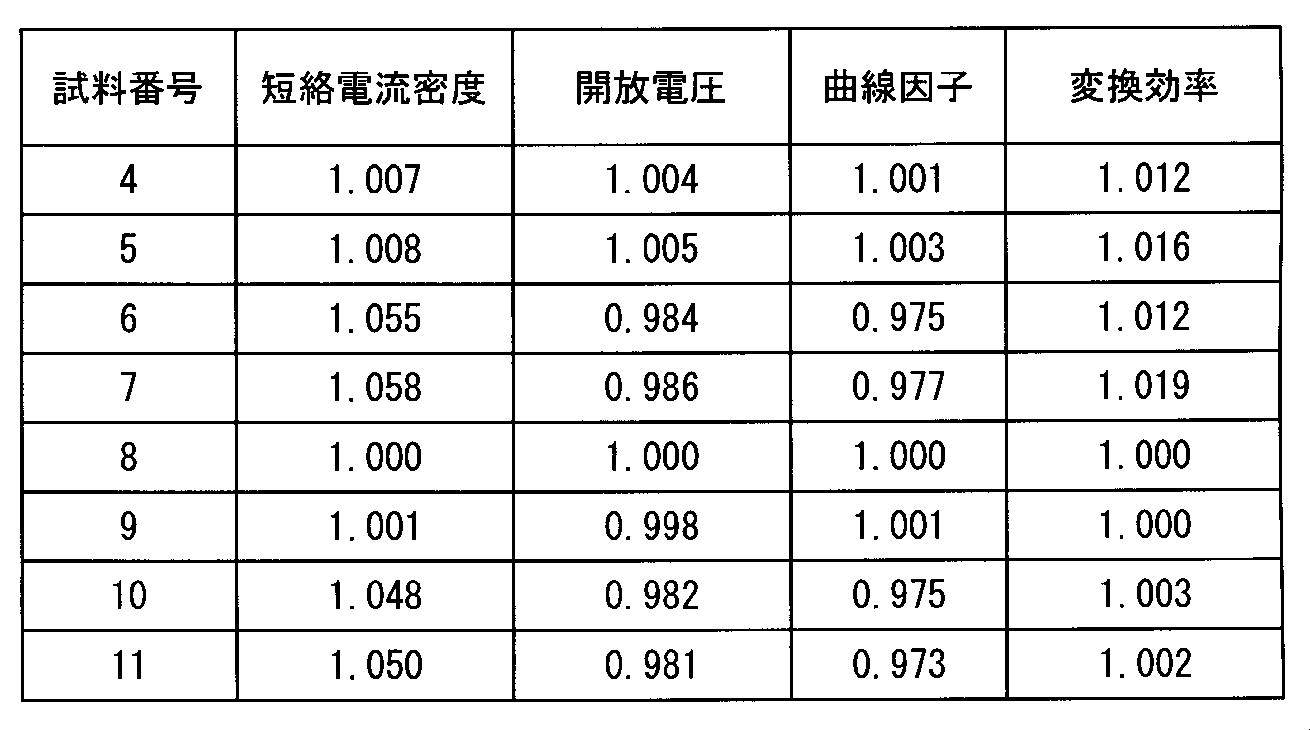
1a,10a 第1主面
1b,10b 第2主面
1aL 凹凸部
2 第1半導体層
3 第2半導体層
4 第3半導体層
5 反射防止層
6 第1電極
6a 第1出力取出電極
6b 第1集電電極
7 第2電極
7a 第2出力取出電極
7b 第2集電電極
10 太陽電池素子
Claims (15)
- 第1導電型の半導体基板の第1主面に酸水溶液によるエッチング処理を施すことで、該半導体基板の前記第1主面に凹凸部を形成する凹凸部形成工程と、
前記半導体基板の前記第1主面側の領域に前記第1導電型とは逆の導電型である第2導電型の半導体層を形成する半導体層形成工程とを有し、
前記凹凸部形成工程は、前記半導体基板の前記第1主面に、フッ酸、硝酸および硫酸を含む第1酸水溶液による第1エッチング処理を施す第1エッチング工程と、該第1エッチング工程の後に、前記半導体基板の前記第1主面に、フッ酸および硝酸を含み且つ硫酸を実質的に含まない第2酸水溶液による第2エッチング処理を施す第2エッチング工程とを有する太陽電池素子の製造方法。 - 前記第2エッチング工程において、前記第1エッチング工程における前記第1酸水溶液の温度よりも低い温度の前記第2酸水溶液によって、前記第2エッチング処理を前記半導体基板の前記第1主面に施す、請求項1に記載の太陽電池素子の製造方法。
- 前記第2エッチング工程において、フッ酸の質量に対する硝酸の質量の比率が前記第1酸水溶液におけるフッ酸の質量に対する硝酸の質量の比率よりも大きい前記第2酸水溶液によって、前記第2エッチング処理を前記半導体基板の前記第1主面に施す、請求項1または請求項2に記載の太陽電池素子の製造方法。
- 前記凹凸部形成工程は、前記第1エッチング工程の後であって前記第2エッチング工程の前に前記半導体基板の前記第1主面の水洗を行う第1水洗工程と、前記第2エッチング工程の後に前記半導体基板の前記第1主面の水洗を行う第2水洗工程とをさらに有し、
前記第2水洗工程において、前記第1水洗工程における水洗の時間よりも長い時間の水洗を行う、請求項1から請求項3のいずれか1つの請求項に記載の太陽電池素子の製造方法。 - 前記第1エッチング工程において、前記半導体基板の前記第1主面と前記第1酸水溶液の液面とが略垂直の関係を有するように、前記半導体基板を前記第1酸水溶液に浸漬する、請求項1から請求項4のいずれか1つの請求項に記載の太陽電池素子の製造方法。
- 半導体材料のインゴットを、砥粒が固着しているワイヤーによって薄切りにして、前記半導体基板を準備する基板準備工程をさらに有する、請求項1から請求項5のいずれか1つの請求項に記載の太陽電池素子の製造方法。
- 熱拡散法によって、第1導電型の半導体基板の第1主面側の領域に該第1導電型とは逆の導電型である第2導電型の半導体層および該半導体層上に配され且つ前記第2導電型に係るドーパントとなる元素を含むガラス層を形成する積層部形成工程と、
フッ酸および塩酸を用いた前記ガラス層の除去を行うガラス層除去工程とを有する太陽電池素子の製造方法。 - 前記ガラス層除去工程において、フッ酸の質量濃度が塩酸の質量濃度の2倍以上で且つ100倍以下である第1混合酸水溶液を用いる、請求項7に記載の太陽電池素子の製造方法。
- 前記積層部形成工程において、前記半導体基板の前記第1主面側の領域および前記第1主面とは逆側の第2主面側の領域に、前記半導体層および該半導体層上に配される前記ガラス層を形成して、
前記積層部形成工程の後であって前記ガラス層除去工程の前に、前記半導体基板の前記第2主面側の領域に形成された前記ガラス層および前記半導体層を除去する積層部除去工程をさらに有し、
該積層部除去工程は、フッ酸および硝酸を含む第2混合酸水溶液を用いて、前記半導体基板の前記第2主面側の領域に形成された前記ガラス層および前記半導体層を除去するとともに、前記第2主面にエッチング処理を施すエッチング工程と、該エッチング工程の後にアルカリ水溶液を用いて前記第2主面を処理する第1アルカリ処理工程とを有している、請求項7または請求項8に記載の太陽電池素子の製造方法。 - 前記エッチング工程において、フッ酸、硝酸および硫酸を含む前記第2混合酸水溶液を用いて、前記半導体基板の前記第2主面側の領域に形成された前記ガラス層および前記半導体層を除去するとともに、前記第2主面に前記エッチング処理を施す、請求項9に記載の太陽電池素子の製造方法。
- 前記積層部形成工程の前に、前記半導体基板の前記第1主面にエッチング処理を施すことによって前記半導体基板の前記第1主面に凹凸部を形成する凹凸部形成工程をさらに有する、請求項7から請求項10のいずれか1つの請求項に記載の太陽電池素子の製造方法。
- 前記凹凸部形成工程は、前記半導体基板の前記第1主面に、フッ酸および硝酸を含む酸水溶液によるエッチング処理を施す第1処理工程と、該第1処理工程の後にアルカリ水溶液を用いて前記第1主面を処理する第2処理工程と、該第2処理工程の後にフッ酸および塩酸を含む混合酸水溶液によるエッチング処理、ならびにフッ酸水溶液および塩酸水溶液によるエッチング処理のうちの少なくとも一方のエッチング処理を前記第1主面に施す第3処理工程とを有する、請求項11に記載の太陽電池素子の製造方法。
- 前記凹凸部形成工程は、前記半導体基板の前記第1主面にエッチング残渣を付着させながらエッチング処理を施す残渣利用エッチング工程と、該残渣利用エッチング工程の後に、フッ酸および塩酸を用いたエッチング処理を前記第1主面に施すことで、該第1主面から前記エッチング残渣を除去する残渣除去工程とを有する、請求項11に記載の太陽電池素子の製造方法。
- 請求項1から請求項13のいずれか1つの請求項に記載の太陽電池素子の製造方法によって製造された太陽電池素子。
- 請求項14に記載の複数の前記太陽電池素子と、
該複数の太陽電池素子を電気的に接続する接続部材とを備える太陽電池モジュール。
Priority Applications (2)
| Application Number | Priority Date | Filing Date | Title |
|---|---|---|---|
| JP2012554858A JP5677469B2 (ja) | 2011-01-27 | 2012-01-27 | 太陽電池素子の製造方法、太陽電池素子、および太陽電池モジュール |
| US13/982,230 US9123840B2 (en) | 2011-01-27 | 2012-01-27 | Solar cell element manufacturing method, solar cell element, and solar cell module |
Applications Claiming Priority (4)
| Application Number | Priority Date | Filing Date | Title |
|---|---|---|---|
| JP2011-014715 | 2011-01-27 | ||
| JP2011014715 | 2011-01-27 | ||
| JP2011042196 | 2011-02-28 | ||
| JP2011-042196 | 2011-02-28 |
Publications (1)
| Publication Number | Publication Date |
|---|---|
| WO2012102368A1 true WO2012102368A1 (ja) | 2012-08-02 |
Family
ID=46580931
Family Applications (1)
| Application Number | Title | Priority Date | Filing Date |
|---|---|---|---|
| PCT/JP2012/051757 Ceased WO2012102368A1 (ja) | 2011-01-27 | 2012-01-27 | 太陽電池素子の製造方法、太陽電池素子、および太陽電池モジュール |
Country Status (3)
| Country | Link |
|---|---|
| US (1) | US9123840B2 (ja) |
| JP (1) | JP5677469B2 (ja) |
| WO (1) | WO2012102368A1 (ja) |
Cited By (4)
| Publication number | Priority date | Publication date | Assignee | Title |
|---|---|---|---|---|
| WO2013049558A3 (en) * | 2011-09-30 | 2013-10-10 | Silicor Materials Inc. | Textured photovoltaic cells and methods |
| WO2014175072A1 (ja) * | 2013-04-26 | 2014-10-30 | 株式会社Tkx | 太陽電池用シリコンウエハー及びその製造方法 |
| JP2014232829A (ja) * | 2013-05-30 | 2014-12-11 | 日本化成株式会社 | 太陽電池用シリコンウエハーの製造方法 |
| JP2015056586A (ja) * | 2013-09-13 | 2015-03-23 | 独立行政法人産業技術総合研究所 | 結晶系シリコン太陽電池及びその製造方法 |
Families Citing this family (4)
| Publication number | Priority date | Publication date | Assignee | Title |
|---|---|---|---|---|
| US9082901B2 (en) * | 2012-04-11 | 2015-07-14 | E I Du Pont De Nemours And Company | Solar cell and manufacturing method of the same |
| CA2953790C (en) | 2014-06-27 | 2021-11-23 | Vidrio Plano De Mexico, S.A. De C.V. | Production method for sheets of glass with a diffuse finish, and resulting sheet of glass |
| CN105576074A (zh) * | 2014-10-08 | 2016-05-11 | 上海神舟新能源发展有限公司 | 一种n型双面电池的湿法刻蚀方法 |
| CN118658915B (zh) * | 2024-08-20 | 2024-11-01 | 金阳(泉州)新能源科技有限公司 | 设置反型隔离结构的联合钝化背接触电池及其制备和应用 |
Citations (3)
| Publication number | Priority date | Publication date | Assignee | Title |
|---|---|---|---|---|
| JP2003258285A (ja) * | 2002-02-27 | 2003-09-12 | Sharp Corp | 表面凹凸構造の作製方法及び太陽電池 |
| JP2003309276A (ja) * | 2002-04-16 | 2003-10-31 | Sharp Corp | 基板の表面加工方法及び太陽電池 |
| JP2005311060A (ja) * | 2004-04-21 | 2005-11-04 | Sharp Corp | 太陽電池の製造方法、太陽電池 |
Family Cites Families (6)
| Publication number | Priority date | Publication date | Assignee | Title |
|---|---|---|---|---|
| US6787692B2 (en) * | 2000-10-31 | 2004-09-07 | National Institute Of Advanced Industrial Science & Technology | Solar cell substrate, thin-film solar cell, and multi-junction thin-film solar cell |
| JP4319006B2 (ja) | 2003-10-23 | 2009-08-26 | シャープ株式会社 | 太陽電池セルの製造方法 |
| JP2005340643A (ja) | 2004-05-28 | 2005-12-08 | Sharp Corp | 太陽電池用半導体基板の製造方法 |
| KR100860367B1 (ko) * | 2006-08-21 | 2008-09-25 | 제일모직주식회사 | 금속실리사이드막 대비 실리콘 산화막에 대한 상대적인 식각 선택성이 향상된 식각용액 |
| JP2008181965A (ja) * | 2007-01-23 | 2008-08-07 | Sharp Corp | 積層型光電変換装置及びその製造方法 |
| TWI559372B (zh) * | 2010-04-06 | 2016-11-21 | 薄膜電子Asa公司 | 磊晶結構、其形成方法及含此結構之元件 |
-
2012
- 2012-01-27 JP JP2012554858A patent/JP5677469B2/ja not_active Expired - Fee Related
- 2012-01-27 US US13/982,230 patent/US9123840B2/en not_active Expired - Fee Related
- 2012-01-27 WO PCT/JP2012/051757 patent/WO2012102368A1/ja not_active Ceased
Patent Citations (3)
| Publication number | Priority date | Publication date | Assignee | Title |
|---|---|---|---|---|
| JP2003258285A (ja) * | 2002-02-27 | 2003-09-12 | Sharp Corp | 表面凹凸構造の作製方法及び太陽電池 |
| JP2003309276A (ja) * | 2002-04-16 | 2003-10-31 | Sharp Corp | 基板の表面加工方法及び太陽電池 |
| JP2005311060A (ja) * | 2004-04-21 | 2005-11-04 | Sharp Corp | 太陽電池の製造方法、太陽電池 |
Cited By (7)
| Publication number | Priority date | Publication date | Assignee | Title |
|---|---|---|---|---|
| WO2013049558A3 (en) * | 2011-09-30 | 2013-10-10 | Silicor Materials Inc. | Textured photovoltaic cells and methods |
| WO2014175072A1 (ja) * | 2013-04-26 | 2014-10-30 | 株式会社Tkx | 太陽電池用シリコンウエハー及びその製造方法 |
| JP2014225633A (ja) * | 2013-04-26 | 2014-12-04 | 株式会社Tkx | 太陽電池用シリコンウエハー及びその製造方法 |
| CN105144351A (zh) * | 2013-04-26 | 2015-12-09 | 株式会社Tkx | 太阳能电池用硅晶圆及其制造方法 |
| CN105144351B (zh) * | 2013-04-26 | 2017-09-26 | 株式会社Tkx | 太阳能电池用硅晶圆及其制造方法 |
| JP2014232829A (ja) * | 2013-05-30 | 2014-12-11 | 日本化成株式会社 | 太陽電池用シリコンウエハーの製造方法 |
| JP2015056586A (ja) * | 2013-09-13 | 2015-03-23 | 独立行政法人産業技術総合研究所 | 結晶系シリコン太陽電池及びその製造方法 |
Also Published As
| Publication number | Publication date |
|---|---|
| US9123840B2 (en) | 2015-09-01 |
| JP5677469B2 (ja) | 2015-02-25 |
| US20140000675A1 (en) | 2014-01-02 |
| JPWO2012102368A1 (ja) | 2014-06-30 |
Similar Documents
| Publication | Publication Date | Title |
|---|---|---|
| JP5677469B2 (ja) | 太陽電池素子の製造方法、太陽電池素子、および太陽電池モジュール | |
| CN101150148B (zh) | 铝背发射结n型单晶硅太阳电池制作工艺 | |
| JP6285545B2 (ja) | 太陽電池素子および太陽電池モジュール | |
| US9171975B2 (en) | Solar cell element and process for production thereof | |
| JP6482692B2 (ja) | 太陽電池素子 | |
| TW201703277A (zh) | 一種局部背接觸太陽能電池的製備方法 | |
| WO2007122897A1 (ja) | インターコネクタ付き太陽電池、太陽電池モジュールおよび太陽電池モジュールの製造方法 | |
| WO2011145731A1 (ja) | 太陽電池素子およびその製造方法ならびに太陽電池モジュール | |
| CN102593263A (zh) | N型晶体硅背发射结太阳能电池的制备方法及腐蚀液 | |
| JP6423373B2 (ja) | 光電変換素子およびそれを備えた太陽電池モジュール | |
| TWI611589B (zh) | 太陽電池及太陽電池模組 | |
| CN105161553A (zh) | 一种新型全背电极晶体硅太阳电池的制备方法 | |
| CN105826408B (zh) | 局部背表面场n型太阳能电池及制备方法和组件、系统 | |
| JP2014011246A (ja) | 太陽電池素子および太陽電池モジュール | |
| WO2016068237A1 (ja) | 太陽電池モジュール | |
| WO2015122257A1 (ja) | 光電変換素子 | |
| JP6430842B2 (ja) | 太陽電池素子の製造方法および太陽電池モジュールの製造方法 | |
| JPWO2009157053A1 (ja) | 光起電力装置およびその製造方法 | |
| JP6502147B2 (ja) | 太陽電池の製造方法および太陽電池モジュールの製造方法 | |
| JP2012256713A (ja) | 太陽電池の製造方法 | |
| CN105304758A (zh) | 一种降低背接触光伏电池贯孔电极处漏电的方法 | |
| JP5920421B2 (ja) | 太陽電池モジュールの製造方法 | |
| CN114628539A (zh) | 一种金刚线切割多晶硅片的制绒方法、制绒硅片及太阳能电池片 | |
| CN102460656B (zh) | 太阳能电池的制造方法 | |
| JP2013089665A (ja) | 太陽電池の製造方法、太陽電池及び太陽電池モジュール |
Legal Events
| Date | Code | Title | Description |
|---|---|---|---|
| 121 | Ep: the epo has been informed by wipo that ep was designated in this application |
Ref document number: 12738745 Country of ref document: EP Kind code of ref document: A1 |
|
| ENP | Entry into the national phase |
Ref document number: 2012554858 Country of ref document: JP Kind code of ref document: A |
|
| WWE | Wipo information: entry into national phase |
Ref document number: 13982230 Country of ref document: US |
|
| NENP | Non-entry into the national phase |
Ref country code: DE |
|
| 122 | Ep: pct application non-entry in european phase |
Ref document number: 12738745 Country of ref document: EP Kind code of ref document: A1 |