WO2012101879A1 - 放射線画像取得装置 - Google Patents
放射線画像取得装置 Download PDFInfo
- Publication number
- WO2012101879A1 WO2012101879A1 PCT/JP2011/074327 JP2011074327W WO2012101879A1 WO 2012101879 A1 WO2012101879 A1 WO 2012101879A1 JP 2011074327 W JP2011074327 W JP 2011074327W WO 2012101879 A1 WO2012101879 A1 WO 2012101879A1
- Authority
- WO
- WIPO (PCT)
- Prior art keywords
- radiation
- incident surface
- image acquisition
- wavelength conversion
- scintillation light
- Prior art date
Links
- 230000005855 radiation Effects 0.000 title claims abstract description 152
- 238000003384 imaging method Methods 0.000 claims abstract description 81
- 238000006243 chemical reaction Methods 0.000 claims abstract description 71
- 230000004044 response Effects 0.000 claims abstract description 4
- 230000003287 optical effect Effects 0.000 claims description 42
- 239000000835 fiber Substances 0.000 claims description 14
- 239000004065 semiconductor Substances 0.000 claims description 14
- 238000007689 inspection Methods 0.000 claims description 5
- 230000008878 coupling Effects 0.000 description 7
- 238000010168 coupling process Methods 0.000 description 7
- 238000005859 coupling reaction Methods 0.000 description 7
- 230000005540 biological transmission Effects 0.000 description 6
- 238000001514 detection method Methods 0.000 description 6
- 230000009977 dual effect Effects 0.000 description 5
- 230000000694 effects Effects 0.000 description 5
- 230000004048 modification Effects 0.000 description 4
- 238000012986 modification Methods 0.000 description 4
- 229910052684 Cerium Inorganic materials 0.000 description 2
- 238000010521 absorption reaction Methods 0.000 description 2
- 238000009792 diffusion process Methods 0.000 description 2
- 238000000926 separation method Methods 0.000 description 2
- 229910052710 silicon Inorganic materials 0.000 description 2
- 239000010703 silicon Substances 0.000 description 2
- 229910052688 Gadolinium Inorganic materials 0.000 description 1
- 229910052771 Terbium Inorganic materials 0.000 description 1
- 230000002238 attenuated effect Effects 0.000 description 1
- 230000008901 benefit Effects 0.000 description 1
- 235000013305 food Nutrition 0.000 description 1
- 230000006870 function Effects 0.000 description 1
- 239000012466 permeate Substances 0.000 description 1
- 230000000007 visual effect Effects 0.000 description 1
Images


Classifications
-
- G—PHYSICS
- G01—MEASURING; TESTING
- G01N—INVESTIGATING OR ANALYSING MATERIALS BY DETERMINING THEIR CHEMICAL OR PHYSICAL PROPERTIES
- G01N23/00—Investigating or analysing materials by the use of wave or particle radiation, e.g. X-rays or neutrons, not covered by groups G01N3/00 – G01N17/00, G01N21/00 or G01N22/00
- G01N23/02—Investigating or analysing materials by the use of wave or particle radiation, e.g. X-rays or neutrons, not covered by groups G01N3/00 – G01N17/00, G01N21/00 or G01N22/00 by transmitting the radiation through the material
- G01N23/04—Investigating or analysing materials by the use of wave or particle radiation, e.g. X-rays or neutrons, not covered by groups G01N3/00 – G01N17/00, G01N21/00 or G01N22/00 by transmitting the radiation through the material and forming images of the material
-
- G—PHYSICS
- G01—MEASURING; TESTING
- G01T—MEASUREMENT OF NUCLEAR OR X-RADIATION
- G01T1/00—Measuring X-radiation, gamma radiation, corpuscular radiation, or cosmic radiation
- G01T1/16—Measuring radiation intensity
- G01T1/20—Measuring radiation intensity with scintillation detectors
-
- G—PHYSICS
- G01—MEASURING; TESTING
- G01T—MEASUREMENT OF NUCLEAR OR X-RADIATION
- G01T1/00—Measuring X-radiation, gamma radiation, corpuscular radiation, or cosmic radiation
- G01T1/16—Measuring radiation intensity
- G01T1/20—Measuring radiation intensity with scintillation detectors
- G01T1/2002—Optical details, e.g. reflecting or diffusing layers
-
- G—PHYSICS
- G01—MEASURING; TESTING
- G01N—INVESTIGATING OR ANALYSING MATERIALS BY DETERMINING THEIR CHEMICAL OR PHYSICAL PROPERTIES
- G01N2223/00—Investigating materials by wave or particle radiation
- G01N2223/60—Specific applications or type of materials
- G01N2223/611—Specific applications or type of materials patterned objects; electronic devices
Definitions
- the present invention relates to a radiation image acquisition apparatus.
- a flat scintillator is irradiated with X-rays emitted from an X-ray source and transmitted through an imaging object, and visible light (scintillation light) emitted from the scintillator is emitted from the scintillator.
- a photodetecting element is coupled to the incident surface of the X-ray and the back surface of the scintillator, and visible light is detected by each of the light detecting element on the incident surface side and the light detecting element on the back surface side. , Increasing the detection efficiency of visible light.
- an apparatus that detects scintillation light on both sides of a scintillator can acquire radiation images in different energy bands on the incident surface side and the back surface side, and so-called dual-energy image acquisition is possible. It becomes possible.
- the radiation that has passed through the object passes through the light detection element on the incident surface side and reaches the scintillator, so that radiation in a relatively low energy band reaches the light detection element on the incident surface side.
- Will be absorbed For example, when the object is formed of light atoms, radiation that has passed through the object may be absorbed by the light detection element on the incident surface side.
- the radiation that has passed through the object is affected by the light detection element on the incident surface side.
- an object of the present invention is to provide a radiographic image acquisition apparatus that can acquire radiographic images of different energy bands and that can reduce the influence on radiation transmitted through an object.
- a radiation image acquisition apparatus includes a radiation source that emits radiation, a flat wavelength conversion member that generates scintillation light in response to incidence of radiation emitted from the radiation source and transmitted through the object,
- the first imaging unit that collects and images the scintillation light emitted in the normal direction of the incident surface from the radiation incident surface of the wavelength conversion member, and the surface opposite to the incident surface of the wavelength conversion member
- second image pickup means for collecting and imaging the scintillation light emitted in the normal direction of the side surface.
- Each is condensed and imaged.
- the first imaging means is disposed at a position separated from the wavelength conversion member in order to collect the scintillation light emitted from the incident surface. Therefore, it can be set as the structure which does not interpose an imaging means between a target object and a wavelength conversion member, and the situation where the imaging means affects the radiation which permeate
- first imaging unit and the second imaging unit collect scintillation light emitted in the normal direction from the incident surface and the opposite surface, respectively, there is no radiation that is free from perspective. An image can be acquired, and calculation between images on the incident surface side and the opposite surface side is facilitated.
- each of the first imaging unit and the second imaging unit includes a condenser lens unit that collects the scintillation light emitted from the wavelength conversion member, an imaging unit that images the collected scintillation light, and The aspect which has this may be sufficient.
- a condenser lens unit that collects the scintillation light emitted from the wavelength conversion member
- an imaging unit that images the collected scintillation light
- the radiation source is arranged so that the angle formed by the optical axis of the radiation source and the incident surface is larger than 0 degree and smaller than 90 degrees, and the first imaging means is arranged on the normal line of the incident surface. It may be an embodiment. In this case, it is possible to directly collect the scintillation light in the normal direction of the incident surface by the first imaging unit and to dispose the first imaging unit from the optical axis of the radiation source. Therefore, the above-described operational effects can be easily realized, and further, the exposure of the first imaging unit due to radiation can be suppressed, and the generation of noise inside the first imaging unit can be suppressed.
- the radiation source is arranged on the normal line of the incident surface, and the first imaging unit is arranged at a position deviated from the normal line of the incident surface, and is arranged between the wavelength conversion member and the radiation source.
- the aspect which condenses scintillation light via a reflective mirror may be sufficient.
- the radiation source since the radiation source is disposed on the normal line of the incident surface, no distortion occurs in the projected image on the wavelength conversion member, and calculation for correcting the tilt of the projected image is not necessary. Furthermore, exposure of the first imaging unit due to radiation can be suppressed, and generation of noise inside the first imaging unit can be suppressed.
- the second imaging means is an aspect in which the scintillation light is collected through a reflection mirror that is disposed at a position deviated from the normal line of the opposite surface and disposed on the normal line of the opposite surface. Also good. In this case, exposure of the second imaging unit due to radiation can be suppressed, and generation of noise inside the second imaging unit can be suppressed. Furthermore, the optical path length from the wavelength conversion member to the first and second imaging means can be adjusted, and the alignment of the first and second imaging means becomes easy. As a result, it becomes easy to match the imaging conditions (simultaneity of imaging timing, identity of imaging position, etc.) of the first and second imaging means.
- a mode in which a tapered fiber is disposed between the opposite surface of the wavelength conversion member and the second imaging unit so as to face the opposite surface may be employed.
- the scintillation light on the opposite surface side can be condensed with high condensing efficiency by the tapered fiber.
- radiation is blocked by the taper fiber, and exposure of the second imaging means can be prevented.
- the object may be a semiconductor device
- the radiation image acquisition apparatus may be applied to a semiconductor failure inspection apparatus that uses the semiconductor device as an inspection target.
- the imaging unit image acquisition device for image acquisition
- radiation images in different energy bands can be acquired, and the influence on radiation transmitted through the object can be reduced.
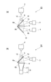
- FIGS. 7A and 7B are front views of a radiological image acquisition apparatus which is a modification of the present invention.
- FIGS. 8A to 8C are front views of a radiographic image acquisition apparatus which is a modification of the present invention.
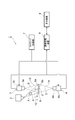
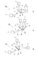
- a radiological image acquisition apparatus 1 is an apparatus for acquiring a radiographic image of an object A such as an electronic component such as a semiconductor device or a food product.
- the radiation image acquisition apparatus 1 generates scintillation light in response to the radiation source 2 that emits radiation such as white X-rays toward the object A and the radiation that is emitted from the radiation source 2 and transmitted through the object A.
- the surface conversion photodetector 6, the surface observation photodetector 3 that collects and images the scintillation light emitted from the radiation incident surface 6 a of the wavelength conversion plate 6, and the surface opposite to the incident surface 6 a.
- a back observation optical detector 4 that collects and images the scintillation light emitted from the back surface 6b.
- the radiation source 2, the wavelength conversion plate 6, the front surface observation photodetector 3, and the back surface observation photodetector 4 are housed in a housing (not shown) and fixed in the housing.
- the wavelength conversion plate 6 is a flat wavelength conversion member, for example, Gd 2 O 2 S: Tb, Gd 2 O 2 S: Pr, CsI: Tl, CdWO 4 , CaWO 4 , Gd 2 SiO 5 : Ce, Lu A scintillator such as 0.4 Gd 1.6 SiO 5 , Bi 4 Ge 3 O 12 , Lu 2 SiO 5 : Ce, Y 2 SiO 5 , YAlO 3 : Ce, Y 2 O 2 S: Tb, YTaO 4 : Tm.
- the thickness of the wavelength conversion plate 6 is set to an appropriate value depending on the energy band of the radiation detected in the range of several ⁇ m to several mm.
- the surface observation photodetector 3 uses the projection image (radiation transmission image) of the object A projected on the wavelength conversion plate 6 as the incident surface 6a side of the wavelength conversion plate 6. This is an indirect conversion type image pickup means for picking up an image.
- the surface detector 3 includes a condensing lens unit 3a that condenses the scintillation light emitted from the incident surface 6a of the wavelength conversion plate 6, and an imaging unit 3b that images the scintillation light collected by the condensing lens unit 3a. , A lens coupling type detector.
- the condensing lens unit 3 a condenses the scintillation light in the surface detector visual field 13.
- a CMOS sensor or a CCD sensor is used as the imaging unit 3b. Note that the light receiving surface of the imaging unit 3b can be substantially parallel to the incident surface 6a.
- the back surface observation light detector 4 projects a projection image (radiation transmission image) of the object A projected on the wavelength conversion plate 6 from the back surface 6b side of the wavelength conversion plate 6.
- This is an indirect conversion type imaging means for imaging.
- the back detector 4 includes a condensing lens unit 4a that condenses the scintillation light emitted from the back surface 6b of the wavelength conversion plate 6, an imaging unit 4b that images the scintillation light collected by the condensing lens unit 4a, This is a lens coupling type detector having the same structure as the surface detector 3 described above.
- the condensing lens unit 4 a condenses the scintillation light in the back detector field of view 14.
- a CMOS sensor or a CCD sensor is used as the imaging unit 4b.
- the light receiving surface of the imaging unit 4b can be substantially parallel to the back surface 6b.
- the radiological image acquisition apparatus 1 inputs a timing control unit 7 that controls imaging timing in the front surface detector 3 and the back surface detector 4 and an image signal output from the front surface detector 3 and the back surface detector 4.
- An image processing device 8 that executes predetermined processing such as image processing based on each of the image signals, and a display device 9 that receives the image signal output from the image processing device 8 and displays a radiation image are provided.
- the timing control unit 7 and the image processing apparatus 8 are configured by a computer having a CPU (Central Processing Unit), a ROM (Read Only Memory), a RAM (Random Access Memory), an input / output interface, and the like.
- a known display is used as the display device 9.
- the timing control unit 7 and the image processing device 8 may be configured as a program executed by a single computer or may be configured as a unit provided individually.
- the radiation source 2 is arranged so that the optical axis X of the radiation forms a predetermined angle ⁇ with respect to the normal B of the incident surface 6 a of the wavelength conversion plate 6. That is, the radiation source 2 faces the object A and the incident surface 6a and is disposed at a position deviating from the normal B of the incident surface 6a. In other words, the radiation source 2 is arranged so that the angle formed by the optical axis X and the incident surface 6a is greater than 0 degree and less than 90 degrees.
- the optical axis X of the radiation is a straight line connecting the radiation emission point of the radiation source 2 and an arbitrary point ⁇ on the incident surface 6 a of the wavelength conversion plate 6.
- an arbitrary point ⁇ is set to be the center point of the incident surface 6a, and in this case, radiation is irradiated relatively uniformly.
- the normal B is a straight line perpendicular to the incident surface 6a extending from an arbitrary point ⁇ on the incident surface 6a.
- an arbitrary point ⁇ is set to be the center point of the incident surface 6a, and the optical axis X and the normal B of the radiation are arbitrary points ⁇ (arbitrary point ⁇ of the incident surface 6a).
- the arbitrary point ⁇ and the arbitrary point ⁇ do not need to be the center point of the incident surface 6a, and need not be the same point.
- the surface detector 3 is arranged so that the optical axis of the built-in condenser lens portion 3a is orthogonal to the incident surface 6a so that the scintillation light emitted from the incident surface 6a of the wavelength conversion plate 6 can be imaged. ing.
- the optical axis of the condensing lens unit 3a coincides with the normal B of the incident surface 6a. That is, the surface detector 3 faces the incident surface 6a and is disposed on the normal B of the incident surface 6a. Therefore, since the surface detector 3 can capture the scintillation light emitted in the normal B direction of the incident surface 6a, it is easy to acquire an image with less tilt.
- the condensing lens unit 3a focuses on the incident surface 6a and collects the scintillation light emitted from the incident surface 6a in the normal B direction toward the imaging unit 3b.
- the surface detector 3 is disposed off the optical axis X of the radiation source 2. That is, the surface detector 3 is arranged so as to be separated from the radiation emission region (region where the radiation bundle 12 exists) from the radiation source 2. As a result, exposure of the surface detector 3 by radiation from the radiation source 2 is prevented, and generation of noise due to generation of a direct radiation conversion signal inside the surface detector 3 is prevented. Further, the surface detector 3 is arranged so that the perpendicular line dropped from the center of the condenser lens portion 3a to the incident surface 6a of the wavelength conversion plate 6 is within the range of the incident surface 6a, and the incident of the wavelength conversion plate 6 It arrange
- the back surface detector 4 is disposed so that the optical axis of the built-in condenser lens portion 4a is orthogonal to the back surface 6b so that the scintillation light emitted from the back surface 6b of the wavelength conversion plate 6 can be imaged.
- the optical axis of the condenser lens portion 4a coincides with the normal C of the back surface 6b. That is, the back surface detector 4 faces the back surface 6b and is disposed on the normal line C of the back surface 6b. Therefore, since the back surface detector 4 can image the scintillation light emitted in the normal C direction of the back surface 6b, it is easy to acquire an image with less tilt.
- the normal C is a straight line extending from an arbitrary point ⁇ on the back surface 6b and perpendicular to the back surface 6b.
- an arbitrary point ⁇ is set as the center point of the back surface 6b, and the arbitrary point ⁇ on the incident surface 6a and the arbitrary point ⁇ on the back surface 6b are located on the same straight line.
- the straight line coincides with the normal B and the normal C.
- the condensing lens unit 4a focuses on the back surface 6b, and condenses the scintillation light emitted from the back surface 6b in the normal C direction toward the imaging unit 4b.
- the optical path length from the incident surface 6 a of the wavelength conversion plate 6 to the front surface detector 3 and the optical path length from the back surface 6 b of the wavelength conversion plate 6 to the back surface detector 4 are equal. Note that the optical path length from the incident surface 6a of the wavelength conversion plate 6 to the surface detector 3 and the optical path length from the back surface 6b of the wavelength conversion plate 6 to the back surface detector 4 may be different. It is necessary to adjust the size of the image by processing or the like.
- control by the timing control unit 7 is performed so that imaging by the front surface detector 3 and the back surface detector 4 is performed simultaneously.
- the imaging timing control of the timing control unit 7 the radiation transmission image of the object A can be imaged in different energy bands. More specifically, the surface detector 3 images a relatively low energy band radiation transmission image, and the back surface detector 4 images a relatively high energy band radiation transmission image. Thereby, dual energy imaging is realized.
- the radiographic image acquisition apparatus 1 it is possible to control the imaging timings of the front surface detector 3 and the back surface detector 4 to be different from each other. Further, the exposure time and the number of shots in the front surface detector 3 and the back surface detector 4 may be controlled to be different.
- the surface detector 3 detects fluorescence (scintillation light) relatively converted on the incident surface 6a side.
- the detection of the fluorescence converted on the incident surface 6a side has features that there is little fluorescence blur and the brightness of the fluorescence is high. This is because in the surface observation, the influence of diffusion and self-absorption inside the wavelength conversion plate 6 can be reduced.
- the back surface detector 4 detects the fluorescence converted relatively on the back surface 6 b side of the wavelength conversion plate 6. Also in this case, the influence of diffusion and self-absorption inside the wavelength conversion plate 6 can be reduced.
- image signals corresponding to the radiation images on both the front and back surfaces are output to the image processing device 8 by the front surface detector 3 and the back surface detector 4, respectively.
- the image processing device 8 performs inter-image operations such as a difference operation and an addition operation based on the input image signal.
- the image signal after image processing is output to the display device 9.
- the display device 9 displays a radiation image corresponding to the input image signal after image processing.
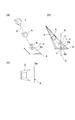
- FIG. 2A is a perspective view showing a positional relationship between the radiation source 2, the object A, and the wavelength conversion plate 6 in the radiation image acquisition apparatus 1, and FIG. 2B is a radiation source 2, the object A, and FIG. 2C is a plan view showing a projection image D of the object A projected on the wavelength conversion plate 6.
- FIG. 2 shows a case where the object A has a cubic shape for easy understanding.
- the radiation source 2 is disposed at a position deviating from the normal B of the incident surface 6a, and the optical axis X of the radiation makes a predetermined angle ⁇ with respect to the normal B of the incident surface 6a. If not, as shown in FIG. 2C, the projected image D on the incident surface 6a is tilted.
- the front surface detector 3 and the back surface detector 4 capture the projected image D from the directions of the normals B and C, respectively, no distortion occurs in the image, and the calculation between the two images in the image processing device 8 is easy. become. Note that the tilt of the projection image D is corrected by the image processing device 8 as necessary.
- the main body of the radiation source 2 is shown to be parallel to the optical axis X, but the direction in which the radiation source 2 is arranged depends on the layout of the apparatus. It can be set appropriately.
- the scintillation light emitted from the incident surface 6a and the back surface 6b of the wavelength conversion plate 6 is condensed by the front surface detector 3 and the back surface detector 4, respectively.
- Dual energy imaging is realized in which radiographs of different energy bands are acquired.
- the surface detector 3 is disposed at a position separated from the wavelength conversion plate 6, and no detector is interposed between the object A and the wavelength conversion plate 6. Therefore, a situation in which the imaging unit affects the radiation transmitted through the object A is avoided. Therefore, the influence on the radiation transmitted through the object A is reduced, and the radiation in the low energy band is suitably detected.
- the shadow of the detector is not reflected in the radiation transmission image, the generation of noise components is suppressed, and the attenuation of the radiation by the detector does not occur, so that the decrease in signal components is suppressed.
- the difference between the low energy band and the high energy band in dual energy imaging can be increased, high energy resolution can be exhibited, and high contrast can be achieved.
- This advantage is particularly remarkable when the object A is formed from silicon or atoms lighter than silicon. That is, even when the object A is formed from light atoms, the low energy band radiation transmitted through the object A is converted into scintillation light without being absorbed or attenuated, and this light is detected on the surface.
- a radiation image in a low energy band can be obtained with high accuracy. Furthermore, a low-energy image and a high-energy image can be simultaneously acquired with a single imaging, ensuring simultaneity, reducing the amount of exposure, and eliminating pixel misregistration (misregistration). Also, dual energy can be realized with one wavelength conversion plate 6.
- the front surface detector 3 and the back surface detector 4 collect scintillation light emitted from the incident surface 6a and the back surface 6b in the normal B and C directions, respectively, so that a radiographic image with no tilt is obtained. The calculation between the images on the incident surface 6a side and the back surface 6b side is facilitated.
- a low-energy image and a high-energy image can be acquired simultaneously with a single white X-ray imaging, ensuring simultaneity, reducing exposure, and pixel misregistration (misregistration). ) Is resolved.
- the scintillation light in the normal B direction of the incident surface 6a is directly condensed by the surface detector 3, and the surface detector 3 is removed from the optical axis X of the radiation source 2, the above-described operation is performed. The effect is easily realized, and further, the exposure of the surface detector 3 due to radiation is prevented, and the generation of noise inside the surface detector 3 is suppressed.
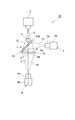
- FIG. 3 is a front view of the radiological image acquisition apparatus according to the second embodiment.
- the radiation image acquisition apparatus 1A shown in FIG. 3 is different from the radiation image acquisition apparatus 1 of the first embodiment shown in FIG. 1 in that the radiation source 2 is arranged on the normal B of the incident surface 6a.
- the surface detector 3 is disposed at a position deviated from the normal line B of the incident surface 6a, and a reflection mirror 15 disposed on the normal line B (optical axis X) between the wavelength conversion plate 6 and the radiation source 2 is provided. It is a point which condenses scintillation light through.
- the timing control unit 7, the image processing device 8, and the display device 9 are not shown.
- illustration of these configurations is omitted.
- the radiation source 2 is arranged so that the optical axis X of the radiation coincides with the normal B of the incident surface 6a.
- the reflecting mirror 15 is arranged such that the reflecting surface 15a forms a predetermined angle (for example, 45 degrees) with respect to the normal B direction, and the scintillation emitted from the incident surface 6a in the normal B direction.
- the light is reflected in a predetermined direction with respect to the normal B.
- an optical mirror that transmits radiation is used as the reflection mirror 15.
- the surface detector 3 is arranged so that the angle formed by the optical axis of the built-in condenser lens portion 3a and the reflection surface 15a is equal to the angle formed by the normal B and the reflection surface 15a.
- the condensing lens unit 3a condenses the scintillation light emitted in the normal B direction from the incident surface 6a and reflected in a predetermined direction with respect to the normal B by the reflecting mirror 15 toward the imaging unit 3b.
- the surface detector 3 is arranged so as to be separated from the radiation emission region (region where the radiation bundle 12 exists) from the radiation source 2. As a result, exposure of the surface detector 3 by radiation from the radiation source 2 is prevented, and generation of noise due to generation of a direct radiation conversion signal inside the surface detector 3 is prevented. Further, the optical path length from the incident surface 6 a of the wavelength conversion plate 6 to the front surface detector 3 and the optical path length from the back surface 6 b of the wavelength conversion plate 6 to the back surface detector 4 may be equal.
- FIG. 4A is a perspective view showing the positional relationship between the radiation source 2, the object A, and the wavelength conversion plate 6 in the radiation image acquisition apparatus 1A
- FIG. 4B is the radiation source 2
- FIG. 4C is a plan view showing a projection image E of the object A projected onto the wavelength conversion plate 6.
- FIG. 4 shows a case where the object A has a cubic shape for easy understanding.
- FIG. 4A when the radiation source 2 is disposed on the normal line B of the incident surface 6a and the optical axis X of the radiation coincides with the normal line B of the incident surface 6a, FIG.
- FIG. 5A no tilt occurs in the projected image E on the incident surface 6a.
- the front surface detector 3 captures the projected image E from the normal B direction via the reflection mirror 15 and the back surface detector 4 captures the projected image E from the normal C direction. Does not occur, and the calculation between the two images in the image processing apparatus 8 is facilitated. Further, since there is no tilt in the projection image E, the tilt correction by the image processing device 8 is not necessary.
- the reflection mirror 15 is disposed on the optical axis X of the radiation source 2, so that radiation is absorbed by the reflection mirror 15.
- the same effects as the radiological image acquisition apparatus 1 can be obtained. Further, since the radiation source 2 is arranged on the normal line B of the incident surface 6a, no distortion occurs in the projection image E onto the wavelength conversion plate 6, and an operation for correcting the inclination of the projection image E becomes unnecessary. ing. Furthermore, exposure of the surface detector 3 due to radiation is prevented, and generation of noise inside the surface detector 3 is prevented.
- FIG. 5 is a front view of the radiation image acquisition apparatus according to the third embodiment.
- the radiological image acquisition apparatus 1B shown in FIG. 5 is different from the radiological image acquisition apparatus 1 of the first embodiment shown in FIG. This is a point where the scintillation light is collected through the reflection mirror 16 arranged on the normal line C. More specifically, the reflecting mirror 16 is disposed such that the reflecting surface 16a forms a predetermined angle (for example, 45 degrees) with respect to the normal C direction, and is emitted from the back surface 6b in the normal C direction. The scintillation light thus reflected is reflected in a predetermined direction with respect to the normal C.
- the reflection mirror 16 for example, an optical mirror or a prism is used.
- the back surface detector 4 is arranged so that the angle formed by the optical axis of the built-in condenser lens portion 4a and the reflection surface 16a is equal to the angle formed by the normal C and the reflection surface 16a.
- the condensing lens unit 4a collects the scintillation light emitted from the back surface 6b in the normal C direction and reflected by the reflecting mirror 16 in the predetermined direction with respect to the normal C toward the imaging unit 4b.
- the back surface detector 4 is arranged so as to be separated from the radiation emission region (region where the radiation bundle 12 exists) from the radiation source 2. As a result, exposure of the back surface detector 4 due to radiation from the radiation source 2 is prevented, and noise is prevented from being generated due to the direct conversion signal of radiation inside the back surface detector 4. Further, the optical path length from the incident surface 6 a of the wavelength conversion plate 6 to the front surface detector 3 and the optical path length from the back surface 6 b of the wavelength conversion plate 6 to the back surface detector 4 may be equal.
- the same effects as the radiation image acquisition apparatuses 1 and 1A are exhibited. Further, exposure of the back surface detector 4 due to radiation is prevented, and generation of noise inside the back surface detector 4 is prevented. Furthermore, the optical path lengths from the wavelength conversion plate 6 to the front surface detector 3 and the back surface detector 4 can be adjusted, and the first and second imaging means can be easily aligned. As a result, it becomes easy to match the imaging conditions (simultaneity of imaging timing, identity of imaging position, etc.) of the first and second imaging means.
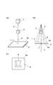
- FIG. 6 is a front view of the radiation image acquisition apparatus according to the fourth embodiment.
- the radiographic image acquisition apparatus 1C shown in FIG. 6 is different from the radiographic image acquisition apparatus 1 of the first embodiment shown in FIG. 1 in that the taper fiber 17 faces the back surface 6b between the back surface 6b and the back surface detector 4. Is the point where is placed. More specifically, the taper fiber 17 is arranged so that the axis thereof coincides with the normal line C of the back surface 6b, and scintillation light emitted from the back surface 6b in the normal C direction is collected by the back surface detector 4. The light is guided to the optical lens unit.
- the tapered fiber 17 and the back surface detector 4 constitute a fiber coupling detector 18.
- the same effects as the radiation image acquisition devices 1, 1A, 1B are exhibited. Further, the scintillation light on the back surface 6b side is condensed with high condensing efficiency by the taper fiber 17. Usually, the fluorescent image on the back surface 6b side of the wavelength conversion plate 6 tends to be dark, but by adopting the fiber coupling detector 18, the loss of the optical system can be reduced. Furthermore, radiation from the radiation source 2 is blocked by the taper fiber 17 and the back surface detector 4 is prevented from being exposed.
- this invention is not limited to the said embodiment.
- the radiation source 2 when the radiation source 2 is disposed on the normal B of the incident surface 6a, various modifications shown in FIG. 7 can be employed. That is, as shown to Fig.7 (a), while setting the reflective mirror 15 in the entrance plane 6a side, it can also be set as the radiographic image acquisition apparatus 1D which has arrange
- the radiation source 2 when the radiation source 2 is disposed at a position deviating from the normal line B of the incident surface 6a, various modifications shown in FIG. 8 can be adopted. That is, as shown to Fig.8 (a), while setting the reflective mirror 15 to the entrance plane 6a side, it can also be set as the radiographic image acquisition apparatus 1F which has arrange
- the reflective mirrors 15 and 16 when using the reflective mirrors 15 and 16, the reflective mirrors 15 and 16 are arrange
- the normal lines B and C are orthogonal to each other has been described, the present invention is not limited to such an arrangement, and the angles of the reflection mirrors 15 and 16 and the arrangement of the front surface detector 3 and the rear surface detector 4 depend on the layout in the apparatus. It can be changed accordingly.
- the radiation source 2 is arranged so that the optical axis X is orthogonal to the incident surface 6a
- the surface detector 3 is arranged so that the optical axis of the condenser lens portion 3a is orthogonal to the incident surface 6a. can do. That is, the optical axis X of the radiation source 2 and the optical axis of the condensing lens unit 3a are parallel to each other, and the distance between these optical axes is equal to the distance between the points ⁇ and ⁇ . Even in such a configuration, the surface detector 3 can collect and image scintillation light emitted in the normal direction of the incident surface 6a.
- the lens coupling type detector is used as the detector.
- the condenser lens unit and the imaging unit may be provided separately.
- the radiation image acquisition apparatus of the above embodiment is a semiconductor fault inspection apparatus in which the object A is a semiconductor device and the semiconductor device is an inspection target.
- the imaging unit image acquisition device for image acquisition
- radiation images in different energy bands can be acquired, and the influence on radiation transmitted through the object can be reduced.
Landscapes
- Physics & Mathematics (AREA)
- Health & Medical Sciences (AREA)
- Life Sciences & Earth Sciences (AREA)
- General Physics & Mathematics (AREA)
- High Energy & Nuclear Physics (AREA)
- Molecular Biology (AREA)
- Spectroscopy & Molecular Physics (AREA)
- Chemical & Material Sciences (AREA)
- Analytical Chemistry (AREA)
- Biochemistry (AREA)
- General Health & Medical Sciences (AREA)
- Immunology (AREA)
- Pathology (AREA)
- Measurement Of Radiation (AREA)
- Analysing Materials By The Use Of Radiation (AREA)
Priority Applications (5)
| Application Number | Priority Date | Filing Date | Title |
|---|---|---|---|
| ES11857086T ES2787256T3 (es) | 2011-01-25 | 2011-10-21 | Dispositivo de adquisición de imágenes de radiación |
| EP11857086.0A EP2669665B1 (en) | 2011-01-25 | 2011-10-21 | Radiation image acquisition device |
| DK11857086.0T DK2669665T3 (da) | 2011-01-25 | 2011-10-21 | Strålingsbilledopfangningsanordning |
| CN201190001001.8U CN203616268U (zh) | 2011-01-25 | 2011-10-21 | 放射线图像取得装置 |
| US13/981,469 US9279890B2 (en) | 2011-01-25 | 2011-10-21 | Radiation image acquisition device |
Applications Claiming Priority (2)
| Application Number | Priority Date | Filing Date | Title |
|---|---|---|---|
| JP2011013192A JP5784916B2 (ja) | 2011-01-25 | 2011-01-25 | 放射線画像取得装置 |
| JP2011-013192 | 2011-01-25 |
Publications (1)
| Publication Number | Publication Date |
|---|---|
| WO2012101879A1 true WO2012101879A1 (ja) | 2012-08-02 |
Family
ID=46580466
Family Applications (1)
| Application Number | Title | Priority Date | Filing Date |
|---|---|---|---|
| PCT/JP2011/074327 WO2012101879A1 (ja) | 2011-01-25 | 2011-10-21 | 放射線画像取得装置 |
Country Status (8)
Cited By (3)
| Publication number | Priority date | Publication date | Assignee | Title |
|---|---|---|---|---|
| WO2014013829A1 (ja) * | 2012-07-20 | 2014-01-23 | 浜松ホトニクス株式会社 | 放射線画像取得装置 |
| JPWO2017056680A1 (ja) * | 2015-09-30 | 2018-07-19 | 浜松ホトニクス株式会社 | 放射線画像取得システムおよび放射線画像取得方法 |
| US10101469B2 (en) | 2011-01-25 | 2018-10-16 | Hamamatsu Photonics K.K. | Radiation image acquisition device |
Families Citing this family (7)
| Publication number | Priority date | Publication date | Assignee | Title |
|---|---|---|---|---|
| EP2919037A1 (fr) * | 2014-03-13 | 2015-09-16 | Université de Technologie de Troyes | Procédé d'optimisation de la collection de photons dans des cristaux scintillateurs, cristal et utilisations associés |
| WO2015198961A1 (ja) * | 2014-06-24 | 2015-12-30 | 株式会社クボタ | 電動機の固定子及び回転電機の冷却構造 |
| CN104155681A (zh) * | 2014-07-21 | 2014-11-19 | 北京辛耕普华医疗科技有限公司 | 用于监测放射源的定位仪及监测放射源的方法 |
| CA3038417A1 (en) | 2016-09-29 | 2018-04-05 | Marel Iceland Ehf. | A method of generating a three dimensional surface profile of a food object |
| KR102592905B1 (ko) * | 2016-12-21 | 2023-10-23 | 삼성전자주식회사 | 엑스선 영상 촬영 장치 및 제어방법 |
| DK3690429T3 (en) * | 2019-02-04 | 2021-12-13 | Microtec Srl | Tunnel ct scanner |
| WO2022113507A1 (ja) | 2020-11-25 | 2022-06-02 | 浜松ホトニクス株式会社 | 撮像ユニット及び撮像システム |
Citations (4)
| Publication number | Priority date | Publication date | Assignee | Title |
|---|---|---|---|---|
| JPH0727866A (ja) | 1993-07-14 | 1995-01-31 | Fuji Photo Film Co Ltd | 放射線検出器 |
| JP2000510729A (ja) * | 1996-05-13 | 2000-08-22 | ユニバーシテイ・オブ・マサチユセツツ・メデイカル・センター | 定量的放射線撮像法のためのシステム |
| JP2005207827A (ja) * | 2004-01-21 | 2005-08-04 | Nagoya Electric Works Co Ltd | X線検査装置、x線検査方法およびx線検査装置の制御プログラム |
| JP2007155653A (ja) * | 2005-12-08 | 2007-06-21 | Olympus Corp | 放射線観察装置 |
Family Cites Families (11)
| Publication number | Priority date | Publication date | Assignee | Title |
|---|---|---|---|---|
| US4578803A (en) * | 1981-12-07 | 1986-03-25 | Albert Macovski | Energy-selective x-ray recording and readout system |
| JPH0795100B2 (ja) | 1986-09-24 | 1995-10-11 | 株式会社日立メデイコ | X線荷物検査装置 |
| JPH05152391A (ja) * | 1991-12-02 | 1993-06-18 | Fujitsu Ltd | X線検査装置 |
| JPH05312734A (ja) * | 1992-05-11 | 1993-11-22 | Fujitsu Ltd | X線検出方法 |
| JPH0861941A (ja) * | 1994-08-23 | 1996-03-08 | Toshiba Corp | 放射線検査装置 |
| JP2000298198A (ja) | 1999-02-08 | 2000-10-24 | Fuji Photo Film Co Ltd | 放射線画像データ取得方法および装置 |
| JP2001004561A (ja) * | 1999-06-17 | 2001-01-12 | On Denshi Kk | 基板検査装置 |
| US7130375B1 (en) * | 2004-01-14 | 2006-10-31 | Xradia, Inc. | High resolution direct-projection type x-ray microtomography system using synchrotron or laboratory-based x-ray source |
| US7405406B1 (en) | 2006-04-21 | 2008-07-29 | Radiation Monitoring Devices, Inc. | Two-sided scintillation detectors and related methods |
| JP4853964B2 (ja) * | 2006-12-28 | 2012-01-11 | 株式会社Ihi検査計測 | X線検査装置用のx線センサ |
| JP2007327967A (ja) * | 2007-07-30 | 2007-12-20 | Toshiba Corp | 放射線弁別測定装置 |
-
2011
- 2011-01-25 JP JP2011013192A patent/JP5784916B2/ja active Active
- 2011-10-21 ES ES11857086T patent/ES2787256T3/es active Active
- 2011-10-21 EP EP11857086.0A patent/EP2669665B1/en active Active
- 2011-10-21 DK DK11857086.0T patent/DK2669665T3/da active
- 2011-10-21 US US13/981,469 patent/US9279890B2/en active Active
- 2011-10-21 WO PCT/JP2011/074327 patent/WO2012101879A1/ja active Application Filing
- 2011-10-21 DE DE202011110808.6U patent/DE202011110808U1/de not_active Expired - Lifetime
- 2011-10-21 CN CN201190001001.8U patent/CN203616268U/zh not_active Expired - Lifetime
Patent Citations (4)
| Publication number | Priority date | Publication date | Assignee | Title |
|---|---|---|---|---|
| JPH0727866A (ja) | 1993-07-14 | 1995-01-31 | Fuji Photo Film Co Ltd | 放射線検出器 |
| JP2000510729A (ja) * | 1996-05-13 | 2000-08-22 | ユニバーシテイ・オブ・マサチユセツツ・メデイカル・センター | 定量的放射線撮像法のためのシステム |
| JP2005207827A (ja) * | 2004-01-21 | 2005-08-04 | Nagoya Electric Works Co Ltd | X線検査装置、x線検査方法およびx線検査装置の制御プログラム |
| JP2007155653A (ja) * | 2005-12-08 | 2007-06-21 | Olympus Corp | 放射線観察装置 |
Cited By (9)
| Publication number | Priority date | Publication date | Assignee | Title |
|---|---|---|---|---|
| US10101469B2 (en) | 2011-01-25 | 2018-10-16 | Hamamatsu Photonics K.K. | Radiation image acquisition device |
| US10746884B2 (en) | 2011-01-25 | 2020-08-18 | Hamamatsu Photonics K.K. | Radiation image acquisition device |
| WO2014013829A1 (ja) * | 2012-07-20 | 2014-01-23 | 浜松ホトニクス株式会社 | 放射線画像取得装置 |
| JP2014021015A (ja) * | 2012-07-20 | 2014-02-03 | Hamamatsu Photonics Kk | 放射線画像取得装置 |
| US9500600B2 (en) | 2012-07-20 | 2016-11-22 | Hamamatsu Photonics K.K. | Radiation image acquisition system |
| US10234406B2 (en) | 2012-07-20 | 2019-03-19 | Hamamatsu Photonics K.K. | Radiation image acquisition system |
| JPWO2017056680A1 (ja) * | 2015-09-30 | 2018-07-19 | 浜松ホトニクス株式会社 | 放射線画像取得システムおよび放射線画像取得方法 |
| US10859715B2 (en) | 2015-09-30 | 2020-12-08 | Hamamatsu Photonics K.K. | Radiation image acquisition system and radiation image acquisition method |
| US11237278B2 (en) | 2015-09-30 | 2022-02-01 | Hamamatsu Photonics K.K. | Radiation image acquisition system and radiation image acquisition method |
Also Published As
| Publication number | Publication date |
|---|---|
| EP2669665A4 (en) | 2017-04-19 |
| US9279890B2 (en) | 2016-03-08 |
| JP2012154733A (ja) | 2012-08-16 |
| JP5784916B2 (ja) | 2015-09-24 |
| ES2787256T3 (es) | 2020-10-15 |
| DE202011110808U1 (de) | 2016-07-14 |
| EP2669665B1 (en) | 2020-04-01 |
| EP2669665A1 (en) | 2013-12-04 |
| DK2669665T3 (da) | 2020-06-02 |
| CN203616268U (zh) | 2014-05-28 |
| US20140016753A1 (en) | 2014-01-16 |
Similar Documents
| Publication | Publication Date | Title |
|---|---|---|
| JP5792472B2 (ja) | 放射線画像取得装置 | |
| JP5784916B2 (ja) | 放射線画像取得装置 | |
| JP5890099B2 (ja) | 放射線画像取得装置 | |
| JP5944254B2 (ja) | 放射線画像取得装置 | |
| US8829449B2 (en) | Scintillator plate | |
| JP5973040B2 (ja) | 放射線画像取得装置 | |
| JP3204649U (ja) | 放射線画像取得装置及び撮像ユニット | |
| JP6671413B2 (ja) | 放射線画像取得装置 | |
| JP5706387B2 (ja) | シンチレータプレート及び画像取得装置 | |
| JP6345720B2 (ja) | 放射線画像取得装置および放射線画像取得装置の調整方法 | |
| WO2022113507A1 (ja) | 撮像ユニット及び撮像システム |
Legal Events
| Date | Code | Title | Description |
|---|---|---|---|
| WWE | Wipo information: entry into national phase |
Ref document number: 201190001001.8 Country of ref document: CN |
|
| 121 | Ep: the epo has been informed by wipo that ep was designated in this application |
Ref document number: 11857086 Country of ref document: EP Kind code of ref document: A1 |
|
| NENP | Non-entry into the national phase |
Ref country code: DE |
|
| WWE | Wipo information: entry into national phase |
Ref document number: 2011857086 Country of ref document: EP |
|
| WWE | Wipo information: entry into national phase |
Ref document number: 13981469 Country of ref document: US |