WO2012101879A1 - Radiation image acquisition device - Google Patents
Radiation image acquisition device Download PDFInfo
- Publication number
- WO2012101879A1 WO2012101879A1 PCT/JP2011/074327 JP2011074327W WO2012101879A1 WO 2012101879 A1 WO2012101879 A1 WO 2012101879A1 JP 2011074327 W JP2011074327 W JP 2011074327W WO 2012101879 A1 WO2012101879 A1 WO 2012101879A1
- Authority
- WO
- WIPO (PCT)
- Prior art keywords
- radiation
- incident surface
- image acquisition
- wavelength conversion
- scintillation light
- Prior art date
Links
Images


Classifications
-
- G—PHYSICS
- G01—MEASURING; TESTING
- G01N—INVESTIGATING OR ANALYSING MATERIALS BY DETERMINING THEIR CHEMICAL OR PHYSICAL PROPERTIES
- G01N23/00—Investigating or analysing materials by the use of wave or particle radiation, e.g. X-rays or neutrons, not covered by groups G01N3/00 – G01N17/00, G01N21/00 or G01N22/00
- G01N23/02—Investigating or analysing materials by the use of wave or particle radiation, e.g. X-rays or neutrons, not covered by groups G01N3/00 – G01N17/00, G01N21/00 or G01N22/00 by transmitting the radiation through the material
- G01N23/04—Investigating or analysing materials by the use of wave or particle radiation, e.g. X-rays or neutrons, not covered by groups G01N3/00 – G01N17/00, G01N21/00 or G01N22/00 by transmitting the radiation through the material and forming images of the material
-
- G—PHYSICS
- G01—MEASURING; TESTING
- G01T—MEASUREMENT OF NUCLEAR OR X-RADIATION
- G01T1/00—Measuring X-radiation, gamma radiation, corpuscular radiation, or cosmic radiation
- G01T1/16—Measuring radiation intensity
- G01T1/20—Measuring radiation intensity with scintillation detectors
-
- G—PHYSICS
- G01—MEASURING; TESTING
- G01T—MEASUREMENT OF NUCLEAR OR X-RADIATION
- G01T1/00—Measuring X-radiation, gamma radiation, corpuscular radiation, or cosmic radiation
- G01T1/16—Measuring radiation intensity
- G01T1/20—Measuring radiation intensity with scintillation detectors
- G01T1/2002—Optical details, e.g. reflecting or diffusing layers
-
- G—PHYSICS
- G01—MEASURING; TESTING
- G01N—INVESTIGATING OR ANALYSING MATERIALS BY DETERMINING THEIR CHEMICAL OR PHYSICAL PROPERTIES
- G01N2223/00—Investigating materials by wave or particle radiation
- G01N2223/60—Specific applications or type of materials
- G01N2223/611—Specific applications or type of materials patterned objects; electronic devices
Definitions
- the present invention relates to a radiation image acquisition apparatus.
- a flat scintillator is irradiated with X-rays emitted from an X-ray source and transmitted through an imaging object, and visible light (scintillation light) emitted from the scintillator is emitted from the scintillator.
- a photodetecting element is coupled to the incident surface of the X-ray and the back surface of the scintillator, and visible light is detected by each of the light detecting element on the incident surface side and the light detecting element on the back surface side. , Increasing the detection efficiency of visible light.
- an apparatus that detects scintillation light on both sides of a scintillator can acquire radiation images in different energy bands on the incident surface side and the back surface side, and so-called dual-energy image acquisition is possible. It becomes possible.
- the radiation that has passed through the object passes through the light detection element on the incident surface side and reaches the scintillator, so that radiation in a relatively low energy band reaches the light detection element on the incident surface side.
- Will be absorbed For example, when the object is formed of light atoms, radiation that has passed through the object may be absorbed by the light detection element on the incident surface side.
- the radiation that has passed through the object is affected by the light detection element on the incident surface side.
- an object of the present invention is to provide a radiographic image acquisition apparatus that can acquire radiographic images of different energy bands and that can reduce the influence on radiation transmitted through an object.
- a radiation image acquisition apparatus includes a radiation source that emits radiation, a flat wavelength conversion member that generates scintillation light in response to incidence of radiation emitted from the radiation source and transmitted through the object,
- the first imaging unit that collects and images the scintillation light emitted in the normal direction of the incident surface from the radiation incident surface of the wavelength conversion member, and the surface opposite to the incident surface of the wavelength conversion member
- second image pickup means for collecting and imaging the scintillation light emitted in the normal direction of the side surface.
- Each is condensed and imaged.
- the first imaging means is disposed at a position separated from the wavelength conversion member in order to collect the scintillation light emitted from the incident surface. Therefore, it can be set as the structure which does not interpose an imaging means between a target object and a wavelength conversion member, and the situation where the imaging means affects the radiation which permeate
- first imaging unit and the second imaging unit collect scintillation light emitted in the normal direction from the incident surface and the opposite surface, respectively, there is no radiation that is free from perspective. An image can be acquired, and calculation between images on the incident surface side and the opposite surface side is facilitated.
- each of the first imaging unit and the second imaging unit includes a condenser lens unit that collects the scintillation light emitted from the wavelength conversion member, an imaging unit that images the collected scintillation light, and The aspect which has this may be sufficient.
- a condenser lens unit that collects the scintillation light emitted from the wavelength conversion member
- an imaging unit that images the collected scintillation light
- the radiation source is arranged so that the angle formed by the optical axis of the radiation source and the incident surface is larger than 0 degree and smaller than 90 degrees, and the first imaging means is arranged on the normal line of the incident surface. It may be an embodiment. In this case, it is possible to directly collect the scintillation light in the normal direction of the incident surface by the first imaging unit and to dispose the first imaging unit from the optical axis of the radiation source. Therefore, the above-described operational effects can be easily realized, and further, the exposure of the first imaging unit due to radiation can be suppressed, and the generation of noise inside the first imaging unit can be suppressed.
- the radiation source is arranged on the normal line of the incident surface, and the first imaging unit is arranged at a position deviated from the normal line of the incident surface, and is arranged between the wavelength conversion member and the radiation source.
- the aspect which condenses scintillation light via a reflective mirror may be sufficient.
- the radiation source since the radiation source is disposed on the normal line of the incident surface, no distortion occurs in the projected image on the wavelength conversion member, and calculation for correcting the tilt of the projected image is not necessary. Furthermore, exposure of the first imaging unit due to radiation can be suppressed, and generation of noise inside the first imaging unit can be suppressed.
- the second imaging means is an aspect in which the scintillation light is collected through a reflection mirror that is disposed at a position deviated from the normal line of the opposite surface and disposed on the normal line of the opposite surface. Also good. In this case, exposure of the second imaging unit due to radiation can be suppressed, and generation of noise inside the second imaging unit can be suppressed. Furthermore, the optical path length from the wavelength conversion member to the first and second imaging means can be adjusted, and the alignment of the first and second imaging means becomes easy. As a result, it becomes easy to match the imaging conditions (simultaneity of imaging timing, identity of imaging position, etc.) of the first and second imaging means.
- a mode in which a tapered fiber is disposed between the opposite surface of the wavelength conversion member and the second imaging unit so as to face the opposite surface may be employed.
- the scintillation light on the opposite surface side can be condensed with high condensing efficiency by the tapered fiber.
- radiation is blocked by the taper fiber, and exposure of the second imaging means can be prevented.
- the object may be a semiconductor device
- the radiation image acquisition apparatus may be applied to a semiconductor failure inspection apparatus that uses the semiconductor device as an inspection target.
- the imaging unit image acquisition device for image acquisition
- radiation images in different energy bands can be acquired, and the influence on radiation transmitted through the object can be reduced.
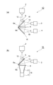
- FIGS. 7A and 7B are front views of a radiological image acquisition apparatus which is a modification of the present invention.
- FIGS. 8A to 8C are front views of a radiographic image acquisition apparatus which is a modification of the present invention.
- a radiological image acquisition apparatus 1 is an apparatus for acquiring a radiographic image of an object A such as an electronic component such as a semiconductor device or a food product.
- the radiation image acquisition apparatus 1 generates scintillation light in response to the radiation source 2 that emits radiation such as white X-rays toward the object A and the radiation that is emitted from the radiation source 2 and transmitted through the object A.
- the surface conversion photodetector 6, the surface observation photodetector 3 that collects and images the scintillation light emitted from the radiation incident surface 6 a of the wavelength conversion plate 6, and the surface opposite to the incident surface 6 a.
- a back observation optical detector 4 that collects and images the scintillation light emitted from the back surface 6b.
- the radiation source 2, the wavelength conversion plate 6, the front surface observation photodetector 3, and the back surface observation photodetector 4 are housed in a housing (not shown) and fixed in the housing.
- the wavelength conversion plate 6 is a flat wavelength conversion member, for example, Gd 2 O 2 S: Tb, Gd 2 O 2 S: Pr, CsI: Tl, CdWO 4 , CaWO 4 , Gd 2 SiO 5 : Ce, Lu A scintillator such as 0.4 Gd 1.6 SiO 5 , Bi 4 Ge 3 O 12 , Lu 2 SiO 5 : Ce, Y 2 SiO 5 , YAlO 3 : Ce, Y 2 O 2 S: Tb, YTaO 4 : Tm.
- the thickness of the wavelength conversion plate 6 is set to an appropriate value depending on the energy band of the radiation detected in the range of several ⁇ m to several mm.
- the surface observation photodetector 3 uses the projection image (radiation transmission image) of the object A projected on the wavelength conversion plate 6 as the incident surface 6a side of the wavelength conversion plate 6. This is an indirect conversion type image pickup means for picking up an image.
- the surface detector 3 includes a condensing lens unit 3a that condenses the scintillation light emitted from the incident surface 6a of the wavelength conversion plate 6, and an imaging unit 3b that images the scintillation light collected by the condensing lens unit 3a. , A lens coupling type detector.
- the condensing lens unit 3 a condenses the scintillation light in the surface detector visual field 13.
- a CMOS sensor or a CCD sensor is used as the imaging unit 3b. Note that the light receiving surface of the imaging unit 3b can be substantially parallel to the incident surface 6a.
- the back surface observation light detector 4 projects a projection image (radiation transmission image) of the object A projected on the wavelength conversion plate 6 from the back surface 6b side of the wavelength conversion plate 6.
- This is an indirect conversion type imaging means for imaging.
- the back detector 4 includes a condensing lens unit 4a that condenses the scintillation light emitted from the back surface 6b of the wavelength conversion plate 6, an imaging unit 4b that images the scintillation light collected by the condensing lens unit 4a, This is a lens coupling type detector having the same structure as the surface detector 3 described above.
- the condensing lens unit 4 a condenses the scintillation light in the back detector field of view 14.
- a CMOS sensor or a CCD sensor is used as the imaging unit 4b.
- the light receiving surface of the imaging unit 4b can be substantially parallel to the back surface 6b.
- the radiological image acquisition apparatus 1 inputs a timing control unit 7 that controls imaging timing in the front surface detector 3 and the back surface detector 4 and an image signal output from the front surface detector 3 and the back surface detector 4.
- An image processing device 8 that executes predetermined processing such as image processing based on each of the image signals, and a display device 9 that receives the image signal output from the image processing device 8 and displays a radiation image are provided.
- the timing control unit 7 and the image processing apparatus 8 are configured by a computer having a CPU (Central Processing Unit), a ROM (Read Only Memory), a RAM (Random Access Memory), an input / output interface, and the like.
- a known display is used as the display device 9.
- the timing control unit 7 and the image processing device 8 may be configured as a program executed by a single computer or may be configured as a unit provided individually.
- the radiation source 2 is arranged so that the optical axis X of the radiation forms a predetermined angle ⁇ with respect to the normal B of the incident surface 6 a of the wavelength conversion plate 6. That is, the radiation source 2 faces the object A and the incident surface 6a and is disposed at a position deviating from the normal B of the incident surface 6a. In other words, the radiation source 2 is arranged so that the angle formed by the optical axis X and the incident surface 6a is greater than 0 degree and less than 90 degrees.
- the optical axis X of the radiation is a straight line connecting the radiation emission point of the radiation source 2 and an arbitrary point ⁇ on the incident surface 6 a of the wavelength conversion plate 6.
- an arbitrary point ⁇ is set to be the center point of the incident surface 6a, and in this case, radiation is irradiated relatively uniformly.
- the normal B is a straight line perpendicular to the incident surface 6a extending from an arbitrary point ⁇ on the incident surface 6a.
- an arbitrary point ⁇ is set to be the center point of the incident surface 6a, and the optical axis X and the normal B of the radiation are arbitrary points ⁇ (arbitrary point ⁇ of the incident surface 6a).
- the arbitrary point ⁇ and the arbitrary point ⁇ do not need to be the center point of the incident surface 6a, and need not be the same point.
- the surface detector 3 is arranged so that the optical axis of the built-in condenser lens portion 3a is orthogonal to the incident surface 6a so that the scintillation light emitted from the incident surface 6a of the wavelength conversion plate 6 can be imaged. ing.
- the optical axis of the condensing lens unit 3a coincides with the normal B of the incident surface 6a. That is, the surface detector 3 faces the incident surface 6a and is disposed on the normal B of the incident surface 6a. Therefore, since the surface detector 3 can capture the scintillation light emitted in the normal B direction of the incident surface 6a, it is easy to acquire an image with less tilt.
- the condensing lens unit 3a focuses on the incident surface 6a and collects the scintillation light emitted from the incident surface 6a in the normal B direction toward the imaging unit 3b.
- the surface detector 3 is disposed off the optical axis X of the radiation source 2. That is, the surface detector 3 is arranged so as to be separated from the radiation emission region (region where the radiation bundle 12 exists) from the radiation source 2. As a result, exposure of the surface detector 3 by radiation from the radiation source 2 is prevented, and generation of noise due to generation of a direct radiation conversion signal inside the surface detector 3 is prevented. Further, the surface detector 3 is arranged so that the perpendicular line dropped from the center of the condenser lens portion 3a to the incident surface 6a of the wavelength conversion plate 6 is within the range of the incident surface 6a, and the incident of the wavelength conversion plate 6 It arrange
- the back surface detector 4 is disposed so that the optical axis of the built-in condenser lens portion 4a is orthogonal to the back surface 6b so that the scintillation light emitted from the back surface 6b of the wavelength conversion plate 6 can be imaged.
- the optical axis of the condenser lens portion 4a coincides with the normal C of the back surface 6b. That is, the back surface detector 4 faces the back surface 6b and is disposed on the normal line C of the back surface 6b. Therefore, since the back surface detector 4 can image the scintillation light emitted in the normal C direction of the back surface 6b, it is easy to acquire an image with less tilt.
- the normal C is a straight line extending from an arbitrary point ⁇ on the back surface 6b and perpendicular to the back surface 6b.
- an arbitrary point ⁇ is set as the center point of the back surface 6b, and the arbitrary point ⁇ on the incident surface 6a and the arbitrary point ⁇ on the back surface 6b are located on the same straight line.
- the straight line coincides with the normal B and the normal C.
- the condensing lens unit 4a focuses on the back surface 6b, and condenses the scintillation light emitted from the back surface 6b in the normal C direction toward the imaging unit 4b.
- the optical path length from the incident surface 6 a of the wavelength conversion plate 6 to the front surface detector 3 and the optical path length from the back surface 6 b of the wavelength conversion plate 6 to the back surface detector 4 are equal. Note that the optical path length from the incident surface 6a of the wavelength conversion plate 6 to the surface detector 3 and the optical path length from the back surface 6b of the wavelength conversion plate 6 to the back surface detector 4 may be different. It is necessary to adjust the size of the image by processing or the like.
- control by the timing control unit 7 is performed so that imaging by the front surface detector 3 and the back surface detector 4 is performed simultaneously.
- the imaging timing control of the timing control unit 7 the radiation transmission image of the object A can be imaged in different energy bands. More specifically, the surface detector 3 images a relatively low energy band radiation transmission image, and the back surface detector 4 images a relatively high energy band radiation transmission image. Thereby, dual energy imaging is realized.
- the radiographic image acquisition apparatus 1 it is possible to control the imaging timings of the front surface detector 3 and the back surface detector 4 to be different from each other. Further, the exposure time and the number of shots in the front surface detector 3 and the back surface detector 4 may be controlled to be different.
- the surface detector 3 detects fluorescence (scintillation light) relatively converted on the incident surface 6a side.
- the detection of the fluorescence converted on the incident surface 6a side has features that there is little fluorescence blur and the brightness of the fluorescence is high. This is because in the surface observation, the influence of diffusion and self-absorption inside the wavelength conversion plate 6 can be reduced.
- the back surface detector 4 detects the fluorescence converted relatively on the back surface 6 b side of the wavelength conversion plate 6. Also in this case, the influence of diffusion and self-absorption inside the wavelength conversion plate 6 can be reduced.
- image signals corresponding to the radiation images on both the front and back surfaces are output to the image processing device 8 by the front surface detector 3 and the back surface detector 4, respectively.
- the image processing device 8 performs inter-image operations such as a difference operation and an addition operation based on the input image signal.
- the image signal after image processing is output to the display device 9.
- the display device 9 displays a radiation image corresponding to the input image signal after image processing.
- FIG. 2A is a perspective view showing a positional relationship between the radiation source 2, the object A, and the wavelength conversion plate 6 in the radiation image acquisition apparatus 1, and FIG. 2B is a radiation source 2, the object A, and FIG. 2C is a plan view showing a projection image D of the object A projected on the wavelength conversion plate 6.
- FIG. 2 shows a case where the object A has a cubic shape for easy understanding.
- the radiation source 2 is disposed at a position deviating from the normal B of the incident surface 6a, and the optical axis X of the radiation makes a predetermined angle ⁇ with respect to the normal B of the incident surface 6a. If not, as shown in FIG. 2C, the projected image D on the incident surface 6a is tilted.
- the front surface detector 3 and the back surface detector 4 capture the projected image D from the directions of the normals B and C, respectively, no distortion occurs in the image, and the calculation between the two images in the image processing device 8 is easy. become. Note that the tilt of the projection image D is corrected by the image processing device 8 as necessary.
- the main body of the radiation source 2 is shown to be parallel to the optical axis X, but the direction in which the radiation source 2 is arranged depends on the layout of the apparatus. It can be set appropriately.
- the scintillation light emitted from the incident surface 6a and the back surface 6b of the wavelength conversion plate 6 is condensed by the front surface detector 3 and the back surface detector 4, respectively.
- Dual energy imaging is realized in which radiographs of different energy bands are acquired.
- the surface detector 3 is disposed at a position separated from the wavelength conversion plate 6, and no detector is interposed between the object A and the wavelength conversion plate 6. Therefore, a situation in which the imaging unit affects the radiation transmitted through the object A is avoided. Therefore, the influence on the radiation transmitted through the object A is reduced, and the radiation in the low energy band is suitably detected.
- the shadow of the detector is not reflected in the radiation transmission image, the generation of noise components is suppressed, and the attenuation of the radiation by the detector does not occur, so that the decrease in signal components is suppressed.
- the difference between the low energy band and the high energy band in dual energy imaging can be increased, high energy resolution can be exhibited, and high contrast can be achieved.
- This advantage is particularly remarkable when the object A is formed from silicon or atoms lighter than silicon. That is, even when the object A is formed from light atoms, the low energy band radiation transmitted through the object A is converted into scintillation light without being absorbed or attenuated, and this light is detected on the surface.
- a radiation image in a low energy band can be obtained with high accuracy. Furthermore, a low-energy image and a high-energy image can be simultaneously acquired with a single imaging, ensuring simultaneity, reducing the amount of exposure, and eliminating pixel misregistration (misregistration). Also, dual energy can be realized with one wavelength conversion plate 6.
- the front surface detector 3 and the back surface detector 4 collect scintillation light emitted from the incident surface 6a and the back surface 6b in the normal B and C directions, respectively, so that a radiographic image with no tilt is obtained. The calculation between the images on the incident surface 6a side and the back surface 6b side is facilitated.
- a low-energy image and a high-energy image can be acquired simultaneously with a single white X-ray imaging, ensuring simultaneity, reducing exposure, and pixel misregistration (misregistration). ) Is resolved.
- the scintillation light in the normal B direction of the incident surface 6a is directly condensed by the surface detector 3, and the surface detector 3 is removed from the optical axis X of the radiation source 2, the above-described operation is performed. The effect is easily realized, and further, the exposure of the surface detector 3 due to radiation is prevented, and the generation of noise inside the surface detector 3 is suppressed.
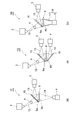
- FIG. 3 is a front view of the radiological image acquisition apparatus according to the second embodiment.
- the radiation image acquisition apparatus 1A shown in FIG. 3 is different from the radiation image acquisition apparatus 1 of the first embodiment shown in FIG. 1 in that the radiation source 2 is arranged on the normal B of the incident surface 6a.
- the surface detector 3 is disposed at a position deviated from the normal line B of the incident surface 6a, and a reflection mirror 15 disposed on the normal line B (optical axis X) between the wavelength conversion plate 6 and the radiation source 2 is provided. It is a point which condenses scintillation light through.
- the timing control unit 7, the image processing device 8, and the display device 9 are not shown.
- illustration of these configurations is omitted.
- the radiation source 2 is arranged so that the optical axis X of the radiation coincides with the normal B of the incident surface 6a.
- the reflecting mirror 15 is arranged such that the reflecting surface 15a forms a predetermined angle (for example, 45 degrees) with respect to the normal B direction, and the scintillation emitted from the incident surface 6a in the normal B direction.
- the light is reflected in a predetermined direction with respect to the normal B.
- an optical mirror that transmits radiation is used as the reflection mirror 15.
- the surface detector 3 is arranged so that the angle formed by the optical axis of the built-in condenser lens portion 3a and the reflection surface 15a is equal to the angle formed by the normal B and the reflection surface 15a.
- the condensing lens unit 3a condenses the scintillation light emitted in the normal B direction from the incident surface 6a and reflected in a predetermined direction with respect to the normal B by the reflecting mirror 15 toward the imaging unit 3b.
- the surface detector 3 is arranged so as to be separated from the radiation emission region (region where the radiation bundle 12 exists) from the radiation source 2. As a result, exposure of the surface detector 3 by radiation from the radiation source 2 is prevented, and generation of noise due to generation of a direct radiation conversion signal inside the surface detector 3 is prevented. Further, the optical path length from the incident surface 6 a of the wavelength conversion plate 6 to the front surface detector 3 and the optical path length from the back surface 6 b of the wavelength conversion plate 6 to the back surface detector 4 may be equal.
- FIG. 4A is a perspective view showing the positional relationship between the radiation source 2, the object A, and the wavelength conversion plate 6 in the radiation image acquisition apparatus 1A
- FIG. 4B is the radiation source 2
- FIG. 4C is a plan view showing a projection image E of the object A projected onto the wavelength conversion plate 6.
- FIG. 4 shows a case where the object A has a cubic shape for easy understanding.
- FIG. 4A when the radiation source 2 is disposed on the normal line B of the incident surface 6a and the optical axis X of the radiation coincides with the normal line B of the incident surface 6a, FIG.
- FIG. 5A no tilt occurs in the projected image E on the incident surface 6a.
- the front surface detector 3 captures the projected image E from the normal B direction via the reflection mirror 15 and the back surface detector 4 captures the projected image E from the normal C direction. Does not occur, and the calculation between the two images in the image processing apparatus 8 is facilitated. Further, since there is no tilt in the projection image E, the tilt correction by the image processing device 8 is not necessary.
- the reflection mirror 15 is disposed on the optical axis X of the radiation source 2, so that radiation is absorbed by the reflection mirror 15.
- the same effects as the radiological image acquisition apparatus 1 can be obtained. Further, since the radiation source 2 is arranged on the normal line B of the incident surface 6a, no distortion occurs in the projection image E onto the wavelength conversion plate 6, and an operation for correcting the inclination of the projection image E becomes unnecessary. ing. Furthermore, exposure of the surface detector 3 due to radiation is prevented, and generation of noise inside the surface detector 3 is prevented.
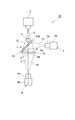
- FIG. 5 is a front view of the radiation image acquisition apparatus according to the third embodiment.
- the radiological image acquisition apparatus 1B shown in FIG. 5 is different from the radiological image acquisition apparatus 1 of the first embodiment shown in FIG. This is a point where the scintillation light is collected through the reflection mirror 16 arranged on the normal line C. More specifically, the reflecting mirror 16 is disposed such that the reflecting surface 16a forms a predetermined angle (for example, 45 degrees) with respect to the normal C direction, and is emitted from the back surface 6b in the normal C direction. The scintillation light thus reflected is reflected in a predetermined direction with respect to the normal C.
- the reflection mirror 16 for example, an optical mirror or a prism is used.
- the back surface detector 4 is arranged so that the angle formed by the optical axis of the built-in condenser lens portion 4a and the reflection surface 16a is equal to the angle formed by the normal C and the reflection surface 16a.
- the condensing lens unit 4a collects the scintillation light emitted from the back surface 6b in the normal C direction and reflected by the reflecting mirror 16 in the predetermined direction with respect to the normal C toward the imaging unit 4b.
- the back surface detector 4 is arranged so as to be separated from the radiation emission region (region where the radiation bundle 12 exists) from the radiation source 2. As a result, exposure of the back surface detector 4 due to radiation from the radiation source 2 is prevented, and noise is prevented from being generated due to the direct conversion signal of radiation inside the back surface detector 4. Further, the optical path length from the incident surface 6 a of the wavelength conversion plate 6 to the front surface detector 3 and the optical path length from the back surface 6 b of the wavelength conversion plate 6 to the back surface detector 4 may be equal.
- the same effects as the radiation image acquisition apparatuses 1 and 1A are exhibited. Further, exposure of the back surface detector 4 due to radiation is prevented, and generation of noise inside the back surface detector 4 is prevented. Furthermore, the optical path lengths from the wavelength conversion plate 6 to the front surface detector 3 and the back surface detector 4 can be adjusted, and the first and second imaging means can be easily aligned. As a result, it becomes easy to match the imaging conditions (simultaneity of imaging timing, identity of imaging position, etc.) of the first and second imaging means.
- FIG. 6 is a front view of the radiation image acquisition apparatus according to the fourth embodiment.
- the radiographic image acquisition apparatus 1C shown in FIG. 6 is different from the radiographic image acquisition apparatus 1 of the first embodiment shown in FIG. 1 in that the taper fiber 17 faces the back surface 6b between the back surface 6b and the back surface detector 4. Is the point where is placed. More specifically, the taper fiber 17 is arranged so that the axis thereof coincides with the normal line C of the back surface 6b, and scintillation light emitted from the back surface 6b in the normal C direction is collected by the back surface detector 4. The light is guided to the optical lens unit.
- the tapered fiber 17 and the back surface detector 4 constitute a fiber coupling detector 18.
- the same effects as the radiation image acquisition devices 1, 1A, 1B are exhibited. Further, the scintillation light on the back surface 6b side is condensed with high condensing efficiency by the taper fiber 17. Usually, the fluorescent image on the back surface 6b side of the wavelength conversion plate 6 tends to be dark, but by adopting the fiber coupling detector 18, the loss of the optical system can be reduced. Furthermore, radiation from the radiation source 2 is blocked by the taper fiber 17 and the back surface detector 4 is prevented from being exposed.
- this invention is not limited to the said embodiment.
- the radiation source 2 when the radiation source 2 is disposed on the normal B of the incident surface 6a, various modifications shown in FIG. 7 can be employed. That is, as shown to Fig.7 (a), while setting the reflective mirror 15 in the entrance plane 6a side, it can also be set as the radiographic image acquisition apparatus 1D which has arrange
- the radiation source 2 when the radiation source 2 is disposed at a position deviating from the normal line B of the incident surface 6a, various modifications shown in FIG. 8 can be adopted. That is, as shown to Fig.8 (a), while setting the reflective mirror 15 to the entrance plane 6a side, it can also be set as the radiographic image acquisition apparatus 1F which has arrange
- the reflective mirrors 15 and 16 when using the reflective mirrors 15 and 16, the reflective mirrors 15 and 16 are arrange
- the normal lines B and C are orthogonal to each other has been described, the present invention is not limited to such an arrangement, and the angles of the reflection mirrors 15 and 16 and the arrangement of the front surface detector 3 and the rear surface detector 4 depend on the layout in the apparatus. It can be changed accordingly.
- the radiation source 2 is arranged so that the optical axis X is orthogonal to the incident surface 6a
- the surface detector 3 is arranged so that the optical axis of the condenser lens portion 3a is orthogonal to the incident surface 6a. can do. That is, the optical axis X of the radiation source 2 and the optical axis of the condensing lens unit 3a are parallel to each other, and the distance between these optical axes is equal to the distance between the points ⁇ and ⁇ . Even in such a configuration, the surface detector 3 can collect and image scintillation light emitted in the normal direction of the incident surface 6a.
- the lens coupling type detector is used as the detector.
- the condenser lens unit and the imaging unit may be provided separately.
- the radiation image acquisition apparatus of the above embodiment is a semiconductor fault inspection apparatus in which the object A is a semiconductor device and the semiconductor device is an inspection target.
- the imaging unit image acquisition device for image acquisition
- radiation images in different energy bands can be acquired, and the influence on radiation transmitted through the object can be reduced.
Abstract
A radiation image acquisition device is provided with a radiation source which emits irradiation, a tabular wavelength conversion member which generates scintillation light in response to the incidence of radiation emitted from the radiation source and transmitted through an object, a first imaging means for capturing images by collecting scintillation light emitted from the radiation incident surface of the wavelength conversion member in the direction normal to said incident surface, and a second imaging means for capturing images by collecting scintillation light emitted from the surface opposite the incident surface of the wavelength conversion member from a direction normal to said opposite surface.
Description
本発明は、放射線画像取得装置に関する。
The present invention relates to a radiation image acquisition apparatus.
従来、下記特許文献1に記載されるように、X線源から発せられて撮像対象物を透過したX線を平板状のシンチレータに照射し、シンチレータで発光した可視光(シンチレーション光)をシンチレータの両面に積層させた固体光検出器により検出し、各固体光検出器から出力された画像信号を重ね合わせて放射線画像を取得する装置が知られている。この装置では、シンチレータにおけるX線の入射面およびその裏面に光検出素子をカップリングさせており、入射面側の光検出素子と裏面側の光検出素子とのそれぞれにおいて可視光を検出することで、可視光の検出効率を高めている。
Conventionally, as described in Patent Document 1 below, a flat scintillator is irradiated with X-rays emitted from an X-ray source and transmitted through an imaging object, and visible light (scintillation light) emitted from the scintillator is emitted from the scintillator. 2. Description of the Related Art There is known an apparatus that obtains a radiation image by superimposing image signals output from each solid-state detector, which are detected by solid-state photodetectors laminated on both sides. In this apparatus, a photodetecting element is coupled to the incident surface of the X-ray and the back surface of the scintillator, and visible light is detected by each of the light detecting element on the incident surface side and the light detecting element on the back surface side. , Increasing the detection efficiency of visible light.
上記のようにシンチレータの両面でシンチレーション光を検出する装置では、入射面側とその裏面側とで異なるエネルギー帯の放射線画像を取得することができ、いわゆるデュアルエナジー(dual-energy)の画像取得が可能となる。
As described above, an apparatus that detects scintillation light on both sides of a scintillator can acquire radiation images in different energy bands on the incident surface side and the back surface side, and so-called dual-energy image acquisition is possible. It becomes possible.
しかしながら、上述した従来の装置では、対象物を透過した放射線は、入射面側の光検出素子を透過してシンチレータに到達するため、比較的低いエネルギー帯の放射線が入射面側の光検出素子に吸収されてしまう。例えば、対象物が軽い原子から形成される場合、対象物を透過した放射線が入射面側の光検出素子によって吸収されることがある。このように、対象物を透過した放射線が入射面側の光検出素子の影響を受けてしまうという問題がある。
However, in the conventional apparatus described above, the radiation that has passed through the object passes through the light detection element on the incident surface side and reaches the scintillator, so that radiation in a relatively low energy band reaches the light detection element on the incident surface side. Will be absorbed. For example, when the object is formed of light atoms, radiation that has passed through the object may be absorbed by the light detection element on the incident surface side. Thus, there is a problem that the radiation that has passed through the object is affected by the light detection element on the incident surface side.
そこで本発明は、異なるエネルギー帯の放射線画像を取得することができ、しかも、対象物を透過した放射線に与える影響を低減することができる放射線画像取得装置を提供することを目的とする。
Therefore, an object of the present invention is to provide a radiographic image acquisition apparatus that can acquire radiographic images of different energy bands and that can reduce the influence on radiation transmitted through an object.
本発明の一形態に係る放射線画像取得装置は、放射線を出射する放射線源と、放射線源から出射され、対象物を透過した放射線の入射に応じてシンチレーション光を発生させる平板状の波長変換部材と、波長変換部材の放射線の入射面から入射面の法線方向に出射されるシンチレーション光を集光して撮像する第1の撮像手段と、波長変換部材の入射面とは反対側の面から反対側の面の法線方向に出射されるシンチレーション光を集光して撮像する第2の撮像手段と、を備えることを特徴とする。
A radiation image acquisition apparatus according to an aspect of the present invention includes a radiation source that emits radiation, a flat wavelength conversion member that generates scintillation light in response to incidence of radiation emitted from the radiation source and transmitted through the object, The first imaging unit that collects and images the scintillation light emitted in the normal direction of the incident surface from the radiation incident surface of the wavelength conversion member, and the surface opposite to the incident surface of the wavelength conversion member And second image pickup means for collecting and imaging the scintillation light emitted in the normal direction of the side surface.
本発明の一形態に係る放射線画像取得装置によれば、第1の撮像手段および第2の撮像手段によって、波長変換部材の放射線の入射面とその反対側の面とから出射されるシンチレーション光がそれぞれ集光され、撮像される。これにより、異なるエネルギー帯の放射線画像を取得するデュアルエナジー撮像が実現される。ここで、第1の撮像手段は、入射面から出射されるシンチレーション光を集光するため、波長変換部材から離間した位置に配置される。よって、対象物と波長変換部材との間に撮像手段が介在しない構成とすることができ、撮像手段が対象物を透過した放射線に影響を与えてしまうような事態を回避できる。従って、対象物を透過した放射線に与える影響を低減することができる。さらには、第1の撮像手段および第2の撮像手段は、入射面およびその反対側の面からそれぞれ法線方向に出射されるシンチレーション光を集光するため、いずれもあおり(perspective)がない放射線画像を取得することができ、入射面側および反対側の面側の画像間における演算が容易になる。
According to the radiological image acquisition apparatus according to one aspect of the present invention, the scintillation light emitted from the radiation incident surface and the opposite surface of the wavelength conversion member by the first imaging unit and the second imaging unit. Each is condensed and imaged. Thereby, dual energy imaging for acquiring radiographic images in different energy bands is realized. Here, the first imaging means is disposed at a position separated from the wavelength conversion member in order to collect the scintillation light emitted from the incident surface. Therefore, it can be set as the structure which does not interpose an imaging means between a target object and a wavelength conversion member, and the situation where the imaging means affects the radiation which permeate | transmitted the target object can be avoided. Therefore, the influence on the radiation transmitted through the object can be reduced. Further, since the first imaging unit and the second imaging unit collect scintillation light emitted in the normal direction from the incident surface and the opposite surface, respectively, there is no radiation that is free from perspective. An image can be acquired, and calculation between images on the incident surface side and the opposite surface side is facilitated.
ここで、第1の撮像手段および第2の撮像手段のそれぞれは、波長変換部材から出射されるシンチレーション光を集光する集光レンズ部と、集光されたシンチレーション光を撮像する撮像部と、を有する態様であってもよい。この場合、波長変換部材の入射面および反対側の面の各面に焦点が合うように集光することで、エネルギー分別が良好で、明るい放射線画像を取得することができる。
Here, each of the first imaging unit and the second imaging unit includes a condenser lens unit that collects the scintillation light emitted from the wavelength conversion member, an imaging unit that images the collected scintillation light, and The aspect which has this may be sufficient. In this case, by condensing so that each of the incident surface and the opposite surface of the wavelength conversion member is in focus, energy separation is good and a bright radiation image can be acquired.
また、放射線源は、放射線源の光軸と入射面とのなす角度が0度より大きく90度より小さくなるように配置されると共に、第1の撮像手段は、入射面の法線上に配置される態様であってもよい。この場合、第1の撮像手段によって入射面の法線方向のシンチレーション光を直接集光すると共に、放射線源の光軸上から第1の撮像手段を外して配置することができる。よって、上記した作用効果を容易に実現でき、さらには、放射線による第1の撮像手段の被曝を抑制することができ、第1の撮像手段の内部におけるノイズの発生を抑制できる。
The radiation source is arranged so that the angle formed by the optical axis of the radiation source and the incident surface is larger than 0 degree and smaller than 90 degrees, and the first imaging means is arranged on the normal line of the incident surface. It may be an embodiment. In this case, it is possible to directly collect the scintillation light in the normal direction of the incident surface by the first imaging unit and to dispose the first imaging unit from the optical axis of the radiation source. Therefore, the above-described operational effects can be easily realized, and further, the exposure of the first imaging unit due to radiation can be suppressed, and the generation of noise inside the first imaging unit can be suppressed.
また、放射線源は、入射面の法線上に配置されると共に、第1の撮像手段は、入射面の法線から外れた位置に配置され、波長変換部材と放射線源との間に配置された反射ミラーを介してシンチレーション光を集光する態様であってもよい。この場合、放射線源が入射面の法線上に配置されるため、波長変換部材への投影像にあおりが生じず、投影像のあおりを補正するための演算が不要となる。さらには、放射線による第1の撮像手段の被曝を抑制することができ、第1の撮像手段の内部におけるノイズの発生を抑制できる。
The radiation source is arranged on the normal line of the incident surface, and the first imaging unit is arranged at a position deviated from the normal line of the incident surface, and is arranged between the wavelength conversion member and the radiation source. The aspect which condenses scintillation light via a reflective mirror may be sufficient. In this case, since the radiation source is disposed on the normal line of the incident surface, no distortion occurs in the projected image on the wavelength conversion member, and calculation for correcting the tilt of the projected image is not necessary. Furthermore, exposure of the first imaging unit due to radiation can be suppressed, and generation of noise inside the first imaging unit can be suppressed.
また、第2の撮像手段は、反対側の面の法線から外れた位置に配置され、反対側の面の法線上に配置された反射ミラーを介してシンチレーション光を集光する態様であってもよい。この場合、放射線による第2の撮像手段の被曝を抑制することができ、第2の撮像手段の内部におけるノイズの発生を抑制できる。さらには、波長変換部材からの第1および第2の撮像手段までの光路長を調整することができ、第1および第2の撮像手段の位置合わせが容易になる。その結果として、第1および第2の撮像手段の撮像条件(撮像タイミングの同時性や撮像位置の同一性など)を合せやすくなる。
Further, the second imaging means is an aspect in which the scintillation light is collected through a reflection mirror that is disposed at a position deviated from the normal line of the opposite surface and disposed on the normal line of the opposite surface. Also good. In this case, exposure of the second imaging unit due to radiation can be suppressed, and generation of noise inside the second imaging unit can be suppressed. Furthermore, the optical path length from the wavelength conversion member to the first and second imaging means can be adjusted, and the alignment of the first and second imaging means becomes easy. As a result, it becomes easy to match the imaging conditions (simultaneity of imaging timing, identity of imaging position, etc.) of the first and second imaging means.
また、波長変換部材の反対側の面と第2の撮像手段との間には、反対側の面に対面させてテーパファイバ(tapered fiber)が配置されている態様であってもよい。この場合、テーパファイバによって反対側の面側のシンチレーション光を高い集光効率で集光できる。さらには、テーパファイバによって放射線が遮断され、第2の撮像手段の被爆を防止することができる。
Further, a mode in which a tapered fiber is disposed between the opposite surface of the wavelength conversion member and the second imaging unit so as to face the opposite surface may be employed. In this case, the scintillation light on the opposite surface side can be condensed with high condensing efficiency by the tapered fiber. Furthermore, radiation is blocked by the taper fiber, and exposure of the second imaging means can be prevented.
また、対象物は半導体デバイスであり、上記放射線画像取得装置は、当該半導体デバイスを検査対象とする半導体故障検査装置に適用される態様であってもよい。この場合、検査対象となる半導体デバイスを透過した放射線が撮像部(画像取得用の撮像素子)によりカットされることがないため、半導体デバイスの故障などを精度良く検出することができる。
Further, the object may be a semiconductor device, and the radiation image acquisition apparatus may be applied to a semiconductor failure inspection apparatus that uses the semiconductor device as an inspection target. In this case, since the radiation that has passed through the semiconductor device to be inspected is not cut by the imaging unit (image acquisition device for image acquisition), a failure of the semiconductor device can be detected with high accuracy.
本発明の一形態によれば、異なるエネルギー帯の放射線画像を取得することができ、かつ、対象物を透過した放射線に与える影響を低減することができる。
According to one aspect of the present invention, radiation images in different energy bands can be acquired, and the influence on radiation transmitted through the object can be reduced.
以下、図面を参照しつつ本発明の実施形態について詳細に説明する。なお、図面の説明においては同一又は相当部分には同一符号を付し、重複する説明を省略する。また、各図面は説明用のために作成されたものであり、説明の対象部位を特に強調するように描かれている。そのため、図面における各部材の寸法比率は、必ずしも実際のものとは一致しない。
Hereinafter, embodiments of the present invention will be described in detail with reference to the drawings. In the description of the drawings, the same or corresponding parts are denoted by the same reference numerals, and redundant description is omitted. Each drawing is made for the purpose of explanation, and is drawn so as to particularly emphasize the target portion of the explanation. Therefore, the dimensional ratio of each member in the drawings does not necessarily match the actual one.
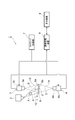
図1に示すように、放射線画像取得装置1は、半導体デバイス等の電子部品や食料品等といった対象物Aの放射線画像を取得するための装置である。放射線画像取得装置1は、対象物Aに向けて白色X線等の放射線を出射する放射線源2と、放射線源2から出射されて対象物Aを透過した放射線の入射に応じてシンチレーション光を発生させる波長変換板6と、波長変換板6の放射線の入射面6aから出射されるシンチレーション光を集光して撮像する表面観察用光検出器3と、入射面6aとは反対側の面である裏面6bから出射されるシンチレーション光を集光して撮像する裏面観察用光検出器4と、を備えている。これらの放射線源2、波長変換板6、表面観察用光検出器3、及び裏面観察用光検出器4は、図示しない筐体に収容され、筐体内で固定される。
As shown in FIG. 1, a radiological image acquisition apparatus 1 is an apparatus for acquiring a radiographic image of an object A such as an electronic component such as a semiconductor device or a food product. The radiation image acquisition apparatus 1 generates scintillation light in response to the radiation source 2 that emits radiation such as white X-rays toward the object A and the radiation that is emitted from the radiation source 2 and transmitted through the object A. The surface conversion photodetector 6, the surface observation photodetector 3 that collects and images the scintillation light emitted from the radiation incident surface 6 a of the wavelength conversion plate 6, and the surface opposite to the incident surface 6 a. A back observation optical detector 4 that collects and images the scintillation light emitted from the back surface 6b. The radiation source 2, the wavelength conversion plate 6, the front surface observation photodetector 3, and the back surface observation photodetector 4 are housed in a housing (not shown) and fixed in the housing.
波長変換板6は、平板状の波長変換部材であり、例えばGd2O2S:Tb、Gd2O2S:Pr、CsI:Tl、CdWO4、CaWO4、Gd2SiO5:Ce、Lu0.4Gd1.6SiO5、Bi4Ge3O12、Lu2SiO5:Ce、Y2SiO5、YAlO3:Ce、Y2O2S:Tb、YTaO4:Tm等のシンチレータである。波長変換板6の厚さは数μm~数mmの範囲で検出する放射線のエネルギー帯によって適切な値に設定されている。
The wavelength conversion plate 6 is a flat wavelength conversion member, for example, Gd 2 O 2 S: Tb, Gd 2 O 2 S: Pr, CsI: Tl, CdWO 4 , CaWO 4 , Gd 2 SiO 5 : Ce, Lu A scintillator such as 0.4 Gd 1.6 SiO 5 , Bi 4 Ge 3 O 12 , Lu 2 SiO 5 : Ce, Y 2 SiO 5 , YAlO 3 : Ce, Y 2 O 2 S: Tb, YTaO 4 : Tm. The thickness of the wavelength conversion plate 6 is set to an appropriate value depending on the energy band of the radiation detected in the range of several μm to several mm.
表面観察用光検出器3(以下、「表面検出器3」と称する)は、波長変換板6に投影された対象物Aの投影像(放射線透過像)を波長変換板6の入射面6a側から撮像する間接変換方式の撮像手段である。表面検出器3は、波長変換板6の入射面6aから出射されるシンチレーション光を集光する集光レンズ部3aと、集光レンズ部3aにより集光されたシンチレーション光を撮像する撮像部3bと、を有するレンズカップリング型の検出器である。集光レンズ部3aは、表面検出器視野13のシンチレーション光を集光する。撮像部3bとしては、例えばCMOSセンサ、CCDセンサ等が用いられる。なお、撮像部3bの受光面は入射面6aに略平行とすることができる。
The surface observation photodetector 3 (hereinafter, referred to as “surface detector 3”) uses the projection image (radiation transmission image) of the object A projected on the wavelength conversion plate 6 as the incident surface 6a side of the wavelength conversion plate 6. This is an indirect conversion type image pickup means for picking up an image. The surface detector 3 includes a condensing lens unit 3a that condenses the scintillation light emitted from the incident surface 6a of the wavelength conversion plate 6, and an imaging unit 3b that images the scintillation light collected by the condensing lens unit 3a. , A lens coupling type detector. The condensing lens unit 3 a condenses the scintillation light in the surface detector visual field 13. For example, a CMOS sensor or a CCD sensor is used as the imaging unit 3b. Note that the light receiving surface of the imaging unit 3b can be substantially parallel to the incident surface 6a.
裏面観察用光検出器4(以下、「裏面検出器4」と称する)は、波長変換板6に投影された対象物Aの投影像(放射線透過像)を波長変換板6の裏面6b側から撮像する間接変換方式の撮像手段である。裏面検出器4は、波長変換板6の裏面6bから出射されるシンチレーション光を集光する集光レンズ部4aと、集光レンズ部4aにより集光されたシンチレーション光を撮像する撮像部4bと、を有するレンズカップリング型の検出器であり、上記の表面検出器3と同様の構成を有している。集光レンズ部4aは、裏面検出器視野14のシンチレーション光を集光する。撮像部4bとしては、例えばCMOSセンサ、CCDセンサ等が用いられる。なお、撮像部4bの受光面は裏面6bに略平行とすることができる。
The back surface observation light detector 4 (hereinafter referred to as “back surface detector 4”) projects a projection image (radiation transmission image) of the object A projected on the wavelength conversion plate 6 from the back surface 6b side of the wavelength conversion plate 6. This is an indirect conversion type imaging means for imaging. The back detector 4 includes a condensing lens unit 4a that condenses the scintillation light emitted from the back surface 6b of the wavelength conversion plate 6, an imaging unit 4b that images the scintillation light collected by the condensing lens unit 4a, This is a lens coupling type detector having the same structure as the surface detector 3 described above. The condensing lens unit 4 a condenses the scintillation light in the back detector field of view 14. For example, a CMOS sensor or a CCD sensor is used as the imaging unit 4b. The light receiving surface of the imaging unit 4b can be substantially parallel to the back surface 6b.
さらに、放射線画像取得装置1は、表面検出器3および裏面検出器4における撮像タイミングを制御するタイミング制御部7と、表面検出器3および裏面検出器4から出力された画像信号を入力し、入力した各画像信号に基づいて画像処理等の所定の処理を実行する画像処理装置8と、画像処理装置8から出力された画像信号を入力し、放射線画像を表示する表示装置9とを備えている。タイミング制御部7および画像処理装置8は、CPU(Central Processing Unit)、ROM(Read Only Memory)、RAM(Random Access Memory)、及び入出力インターフェイス等を有するコンピュータから構成される。表示装置9としては、公知のディスプレイが用いられる。なお、タイミング制御部7および画像処理装置8は、単一のコンピュータにより実行されるプログラムとして構成してもよいし、個別に設けられるユニットとして構成してもよい。
Further, the radiological image acquisition apparatus 1 inputs a timing control unit 7 that controls imaging timing in the front surface detector 3 and the back surface detector 4 and an image signal output from the front surface detector 3 and the back surface detector 4. An image processing device 8 that executes predetermined processing such as image processing based on each of the image signals, and a display device 9 that receives the image signal output from the image processing device 8 and displays a radiation image are provided. . The timing control unit 7 and the image processing apparatus 8 are configured by a computer having a CPU (Central Processing Unit), a ROM (Read Only Memory), a RAM (Random Access Memory), an input / output interface, and the like. A known display is used as the display device 9. The timing control unit 7 and the image processing device 8 may be configured as a program executed by a single computer or may be configured as a unit provided individually.
続いて、上記した放射線源2、波長変換板6、表面検出器3、及び裏面検出器4の位置関係について説明する。図1に示すように、放射線源2は、放射線の光軸Xが波長変換板6の入射面6aの法線Bに対して所定の角度θをなすように配置されている。すなわち、放射線源2は、対象物Aおよび入射面6aに対峙すると共に、入射面6aの法線Bから外れた位置に配置されている。換言すれば、放射線源2は、光軸Xと入射面6aとのなす角度が0度より大きく90度より小さくなるように配置されている。ここで、放射線の光軸Xとは、放射線源2の放射線出射点と波長変換板6の入射面6a上の任意の点γとを結ぶ直線である。本実施形態では、任意の点γが入射面6aの中心点となるように設定されており、この場合、比較的むらなく放射線が照射される。また、法線Bとは、入射面6a上の任意の点αから延びる入射面6aに対して垂直な直線である。本実施形態では、任意の点αが入射面6aの中心点となるように設定されており、放射線の光軸Xと法線Bとは、入射面6aの任意の点γ(任意の点α)で交わる。もちろん、任意の点γおよび任意の点αは入射面6aの中心点である必要はなく、同一の点である必要もない。
Subsequently, the positional relationship between the radiation source 2, the wavelength conversion plate 6, the front surface detector 3, and the back surface detector 4 will be described. As shown in FIG. 1, the radiation source 2 is arranged so that the optical axis X of the radiation forms a predetermined angle θ with respect to the normal B of the incident surface 6 a of the wavelength conversion plate 6. That is, the radiation source 2 faces the object A and the incident surface 6a and is disposed at a position deviating from the normal B of the incident surface 6a. In other words, the radiation source 2 is arranged so that the angle formed by the optical axis X and the incident surface 6a is greater than 0 degree and less than 90 degrees. Here, the optical axis X of the radiation is a straight line connecting the radiation emission point of the radiation source 2 and an arbitrary point γ on the incident surface 6 a of the wavelength conversion plate 6. In the present embodiment, an arbitrary point γ is set to be the center point of the incident surface 6a, and in this case, radiation is irradiated relatively uniformly. The normal B is a straight line perpendicular to the incident surface 6a extending from an arbitrary point α on the incident surface 6a. In the present embodiment, an arbitrary point α is set to be the center point of the incident surface 6a, and the optical axis X and the normal B of the radiation are arbitrary points γ (arbitrary point α of the incident surface 6a). ) Of course, the arbitrary point γ and the arbitrary point α do not need to be the center point of the incident surface 6a, and need not be the same point.
表面検出器3は、波長変換板6の入射面6aから出射されたシンチレーション光を撮像可能なように、内蔵する集光レンズ部3aの光軸が入射面6aに対して直交するように配置されている。ここで、集光レンズ部3aの光軸は、入射面6aの法線Bに一致している。すなわち、表面検出器3は、入射面6aに対峙すると共に、入射面6aの法線B上に配置されている。従って、表面検出器3は、入射面6aの法線B方向に出射されたシンチレーション光を撮像可能であるため、あおりの少ない画像を取得しやすい。集光レンズ部3aは、入射面6a上に焦点を合わせ、入射面6aから法線B方向に出射されたシンチレーション光を撮像部3bに向けて集光する。
The surface detector 3 is arranged so that the optical axis of the built-in condenser lens portion 3a is orthogonal to the incident surface 6a so that the scintillation light emitted from the incident surface 6a of the wavelength conversion plate 6 can be imaged. ing. Here, the optical axis of the condensing lens unit 3a coincides with the normal B of the incident surface 6a. That is, the surface detector 3 faces the incident surface 6a and is disposed on the normal B of the incident surface 6a. Therefore, since the surface detector 3 can capture the scintillation light emitted in the normal B direction of the incident surface 6a, it is easy to acquire an image with less tilt. The condensing lens unit 3a focuses on the incident surface 6a and collects the scintillation light emitted from the incident surface 6a in the normal B direction toward the imaging unit 3b.
上記のようにして、表面検出器3は、放射線源2の光軸X上から外して配置されている。すなわち、表面検出器3は、放射線源2からの放射線の出射領域(放射線束12が存在する領域)から離れるように配置されている。これにより、放射線源2からの放射線による表面検出器3の被曝が防止され、表面検出器3の内部で放射線の直接変換信号が生じてノイズが発生することが防止されている。また、表面検出器3は、集光レンズ部3aの中心から波長変換板6の入射面6aに降ろした垂線が入射面6aの範囲内であるように配置され、かつ、波長変換板6の入射面6a上方に配置されている。これにより、比較的多くのシンチレーション光を検出可能となる。
As described above, the surface detector 3 is disposed off the optical axis X of the radiation source 2. That is, the surface detector 3 is arranged so as to be separated from the radiation emission region (region where the radiation bundle 12 exists) from the radiation source 2. As a result, exposure of the surface detector 3 by radiation from the radiation source 2 is prevented, and generation of noise due to generation of a direct radiation conversion signal inside the surface detector 3 is prevented. Further, the surface detector 3 is arranged so that the perpendicular line dropped from the center of the condenser lens portion 3a to the incident surface 6a of the wavelength conversion plate 6 is within the range of the incident surface 6a, and the incident of the wavelength conversion plate 6 It arrange | positions above the surface 6a. Thereby, a relatively large amount of scintillation light can be detected.
裏面検出器4は、波長変換板6の裏面6bから出射されたシンチレーション光を撮像可能なように、内蔵する集光レンズ部4aの光軸が裏面6bに対して直交するように配置されている。ここで、集光レンズ部4aの光軸は、裏面6bの法線Cに一致している。すなわち、裏面検出器4は、裏面6bに対峙すると共に、裏面6bの法線C上に配置されている。従って、裏面検出器4は、裏面6bの法線C方向に出射されたシンチレーション光を撮像可能であるため、あおりの少ない画像を取得しやすい。ここで、法線Cとは、裏面6b上の任意の点βから延び、裏面6bに対して垂直な直線である。特に、本実施形態では、任意の点βが裏面6bの中心点に設定されており、入射面6a上の任意の点αと裏面6b上の任意の点βは同一直線上に位置し、この直線は法線Bと法線Cに一致する。集光レンズ部4aは、裏面6b上に焦点を合わせ、裏面6bから法線C方向に出射されたシンチレーション光を撮像部4bに向けて集光する。
The back surface detector 4 is disposed so that the optical axis of the built-in condenser lens portion 4a is orthogonal to the back surface 6b so that the scintillation light emitted from the back surface 6b of the wavelength conversion plate 6 can be imaged. . Here, the optical axis of the condenser lens portion 4a coincides with the normal C of the back surface 6b. That is, the back surface detector 4 faces the back surface 6b and is disposed on the normal line C of the back surface 6b. Therefore, since the back surface detector 4 can image the scintillation light emitted in the normal C direction of the back surface 6b, it is easy to acquire an image with less tilt. Here, the normal C is a straight line extending from an arbitrary point β on the back surface 6b and perpendicular to the back surface 6b. In particular, in the present embodiment, an arbitrary point β is set as the center point of the back surface 6b, and the arbitrary point α on the incident surface 6a and the arbitrary point β on the back surface 6b are located on the same straight line. The straight line coincides with the normal B and the normal C. The condensing lens unit 4a focuses on the back surface 6b, and condenses the scintillation light emitted from the back surface 6b in the normal C direction toward the imaging unit 4b.
放射線画像取得装置1では、波長変換板6の入射面6aから表面検出器3までの光路長と、波長変換板6の裏面6bから裏面検出器4までの光路長とは、等しくなっている。なお、波長変換板6の入射面6aから表面検出器3までの光路長と、波長変換板6の裏面6bから裏面検出器4までの光路長とは異なっていてもよいが、この場合、画像処理等により画像の大きさなどを合わせる必要がある。
In the radiation image acquisition apparatus 1, the optical path length from the incident surface 6 a of the wavelength conversion plate 6 to the front surface detector 3 and the optical path length from the back surface 6 b of the wavelength conversion plate 6 to the back surface detector 4 are equal. Note that the optical path length from the incident surface 6a of the wavelength conversion plate 6 to the surface detector 3 and the optical path length from the back surface 6b of the wavelength conversion plate 6 to the back surface detector 4 may be different. It is necessary to adjust the size of the image by processing or the like.
続いて、上記の構成を有する放射線画像取得装置1の動作について説明する。まず、表面検出器3および裏面検出器4による撮像が同時に行われるよう、タイミング制御部7による制御が行われる。タイミング制御部7の撮像タイミング制御により、対象物Aの放射線透過像を異なるエネルギー帯で画像化することができる。詳述すると、表面検出器3によって比較的低いエネルギー帯の放射線透過像が画像化され、また、裏面検出器4によって比較的高いエネルギー帯の放射線透過像が画像化される。これにより、デュアルエナジー撮像が実現される。なお、放射線画像取得装置1では、表面検出器3と裏面検出器4との撮像タイミングをそれぞれ異なるように制御することが可能である。また、表面検出器3と裏面検出器4とのそれぞれにおける露光時間や撮影枚数が異なるように制御してもよい。
Subsequently, the operation of the radiation image acquisition apparatus 1 having the above configuration will be described. First, control by the timing control unit 7 is performed so that imaging by the front surface detector 3 and the back surface detector 4 is performed simultaneously. By the imaging timing control of the timing control unit 7, the radiation transmission image of the object A can be imaged in different energy bands. More specifically, the surface detector 3 images a relatively low energy band radiation transmission image, and the back surface detector 4 images a relatively high energy band radiation transmission image. Thereby, dual energy imaging is realized. In the radiographic image acquisition apparatus 1, it is possible to control the imaging timings of the front surface detector 3 and the back surface detector 4 to be different from each other. Further, the exposure time and the number of shots in the front surface detector 3 and the back surface detector 4 may be controlled to be different.
表面検出器3および裏面検出器4の機能に関し、換言すると、表面検出器3によって、比較的入射面6a側で変換された蛍光(シンチレーション光)が検出される。入射面6a側で変換された蛍光の検出は、蛍光のボケ(blur)が少なく、また、蛍光の輝度が高いといった特長を有する。これは、表面観察においては、波長変換板6の内部における拡散や自己吸収の影響を低減できるためである。一方、裏面検出器4では、波長変換板6の比較的裏面6b側で変換された蛍光が検出される。この場合も、波長変換板6の内部における拡散や自己吸収の影響を低減できる。
Regarding the functions of the front surface detector 3 and the back surface detector 4, in other words, the surface detector 3 detects fluorescence (scintillation light) relatively converted on the incident surface 6a side. The detection of the fluorescence converted on the incident surface 6a side has features that there is little fluorescence blur and the brightness of the fluorescence is high. This is because in the surface observation, the influence of diffusion and self-absorption inside the wavelength conversion plate 6 can be reduced. On the other hand, the back surface detector 4 detects the fluorescence converted relatively on the back surface 6 b side of the wavelength conversion plate 6. Also in this case, the influence of diffusion and self-absorption inside the wavelength conversion plate 6 can be reduced.
次に、表面検出器3および裏面検出器4のそれぞれによって、表裏両面の放射線画像に対応する画像信号が画像処理装置8に出力される。表面検出器3および裏面検出器4のそれぞれから出力された画像信号が画像処理装置8に入力されると、画像処理装置8によって、入力した画像信号に基づいて差分演算や加算演算といった画像間演算などの所定の処理が実行され、画像処理後の画像信号が表示装置9に出力される。そして、画像処理装置8から出力された画像処理後の画像信号が表示装置9に入力されると、表示装置9によって、入力した画像処理後の画像信号に応じた放射線画像が表示される。
Next, image signals corresponding to the radiation images on both the front and back surfaces are output to the image processing device 8 by the front surface detector 3 and the back surface detector 4, respectively. When the image signal output from each of the front surface detector 3 and the back surface detector 4 is input to the image processing device 8, the image processing device 8 performs inter-image operations such as a difference operation and an addition operation based on the input image signal. The image signal after image processing is output to the display device 9. Then, when the image signal after image processing output from the image processing device 8 is input to the display device 9, the display device 9 displays a radiation image corresponding to the input image signal after image processing.
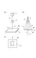
図2(a)は、放射線画像取得装置1における放射線源2、対象物A、及び波長変換板6の位置関係を示す斜視図、図2(b)は、放射線源2、対象物A、及び波長変換板6の位置関係を示す正面図、図2(c)は、波長変換板6に投影される対象物Aの投影像Dを示す平面図である。図2では、理解を容易にするために、対象物Aが立方体形状である場合について示している。図2(a)に示すように、放射線源2が入射面6aの法線Bから外れた位置に配置され、放射線の光軸Xが入射面6aの法線Bに対して所定の角度θをなしていると、図2(c)に示すように、入射面6a上への投影像Dにはあおりが生じることとなる。そして、表面検出器3および裏面検出器4では、投影像Dをそれぞれ法線B,C方向から撮像するため、画像にはあおりが生じず、画像処理装置8での両画像間における演算が容易になる。なお、投影像Dのあおりは、画像処理装置8によって、必要に応じて補正される。なお図2(a)では、説明の便宜上、放射線源2の本体が光軸Xに対して平行となるよう図示されているが、放射線源2が配置される向きは、装置のレイアウトに応じて適宜設定することができる。
2A is a perspective view showing a positional relationship between the radiation source 2, the object A, and the wavelength conversion plate 6 in the radiation image acquisition apparatus 1, and FIG. 2B is a radiation source 2, the object A, and FIG. 2C is a plan view showing a projection image D of the object A projected on the wavelength conversion plate 6. FIG. 2 shows a case where the object A has a cubic shape for easy understanding. As shown in FIG. 2A, the radiation source 2 is disposed at a position deviating from the normal B of the incident surface 6a, and the optical axis X of the radiation makes a predetermined angle θ with respect to the normal B of the incident surface 6a. If not, as shown in FIG. 2C, the projected image D on the incident surface 6a is tilted. Since the front surface detector 3 and the back surface detector 4 capture the projected image D from the directions of the normals B and C, respectively, no distortion occurs in the image, and the calculation between the two images in the image processing device 8 is easy. become. Note that the tilt of the projection image D is corrected by the image processing device 8 as necessary. In FIG. 2A, for convenience of explanation, the main body of the radiation source 2 is shown to be parallel to the optical axis X, but the direction in which the radiation source 2 is arranged depends on the layout of the apparatus. It can be set appropriately.
以上説明した本実施形態の放射線画像取得装置1によれば、表面検出器3および裏面検出器4によって、波長変換板6の入射面6aと裏面6bとから出射されるシンチレーション光がそれぞれ集光され、撮像され、異なるエネルギー帯の放射線画像を取得するデュアルエナジー撮像が実現される。ここで、表面検出器3は、波長変換板6から離間した位置に配置されており、対象物Aと波長変換板6との間には検出器が何ら介在していない。よって、撮像手段が対象物Aを透過した放射線に影響を与えてしまうような事態が回避される。従って、対象物Aを透過した放射線に与える影響が低減され、低エネルギー帯の放射線が好適に検出される。換言すれば、放射線透過像に検出器の影が映り込まないため、ノイズ成分の発生が抑制されると共に、検出器による放射線の減衰も生じないため、信号成分の減少が抑制される。その結果として、デュアルエナジー撮像における低エネルギー帯と高エネルギー帯との差を大きくでき、高度なエネルギー分解能が発揮され、高コントラスト化を図ることができる。この利点は、対象物Aがシリコンもしくはシリコンより軽い原子から形成される場合、特に顕著に発揮される。すなわち、対象物Aが軽い原子から形成される場合であっても、対象物Aを透過した低エネルギー帯の放射線が吸収されたり減衰したりすることなくシンチレーション光に変換され、この光が表面検出器3によって撮像されるため、低エネルギー帯の放射線画像を精度良く取得することができる。さらにまた、一回の撮像で低エネルギー画像と高エネルギー画像を同時に取得でき、同時性の確保、被爆量の低減、及び画素ずれ(ミスレジストレーション(misregistration))の解消が図られる。また、1枚の波長変換板6でもデュアルエナジー化が実現される。しかも、表面検出器3および裏面検出器4は、入射面6aおよび裏面6bからそれぞれ法線B,C方向に出射されるシンチレーション光を集光するため、いずれもあおりがない放射線画像を取得することができ、入射面6a側および裏面6b側の画像間における演算が容易になる。
According to the radiological image acquisition apparatus 1 of the present embodiment described above, the scintillation light emitted from the incident surface 6a and the back surface 6b of the wavelength conversion plate 6 is condensed by the front surface detector 3 and the back surface detector 4, respectively. Dual energy imaging is realized in which radiographs of different energy bands are acquired. Here, the surface detector 3 is disposed at a position separated from the wavelength conversion plate 6, and no detector is interposed between the object A and the wavelength conversion plate 6. Therefore, a situation in which the imaging unit affects the radiation transmitted through the object A is avoided. Therefore, the influence on the radiation transmitted through the object A is reduced, and the radiation in the low energy band is suitably detected. In other words, since the shadow of the detector is not reflected in the radiation transmission image, the generation of noise components is suppressed, and the attenuation of the radiation by the detector does not occur, so that the decrease in signal components is suppressed. As a result, the difference between the low energy band and the high energy band in dual energy imaging can be increased, high energy resolution can be exhibited, and high contrast can be achieved. This advantage is particularly remarkable when the object A is formed from silicon or atoms lighter than silicon. That is, even when the object A is formed from light atoms, the low energy band radiation transmitted through the object A is converted into scintillation light without being absorbed or attenuated, and this light is detected on the surface. Since the image is taken by the device 3, a radiation image in a low energy band can be obtained with high accuracy. Furthermore, a low-energy image and a high-energy image can be simultaneously acquired with a single imaging, ensuring simultaneity, reducing the amount of exposure, and eliminating pixel misregistration (misregistration). Also, dual energy can be realized with one wavelength conversion plate 6. In addition, the front surface detector 3 and the back surface detector 4 collect scintillation light emitted from the incident surface 6a and the back surface 6b in the normal B and C directions, respectively, so that a radiographic image with no tilt is obtained. The calculation between the images on the incident surface 6a side and the back surface 6b side is facilitated.
また、放射線として白色X線を用いる場合でも、白色X線の一回の撮像で低エネルギー画像と高エネルギー画像を同時に取得でき、同時性の確保、被爆量の低減、及び画素ずれ(ミスレジストレーション)の解消が図られる。
In addition, even when white X-rays are used as radiation, a low-energy image and a high-energy image can be acquired simultaneously with a single white X-ray imaging, ensuring simultaneity, reducing exposure, and pixel misregistration (misregistration). ) Is resolved.
また、波長変換板6の入射面6aおよび裏面6bの各面に焦点が合うように、集光レンズ部3aおよび集光レンズ部4aによって集光することで、エネルギー分別が良好で、明るい放射線画像を取得できる。
In addition, by collecting light by the condensing lens unit 3a and the condensing lens unit 4a so that the respective surfaces of the incident surface 6a and the back surface 6b of the wavelength conversion plate 6 are focused, a bright radiation image with good energy separation. Can be obtained.
また、表面検出器3によって入射面6aの法線B方向のシンチレーション光を直接集光すると共に、放射線源2の光軸X上から表面検出器3を外して配置しているため、上記した作用効果が容易に実現され、さらには、放射線による表面検出器3の被曝が防止され、表面検出器3の内部におけるノイズの発生が抑制される。
Further, since the scintillation light in the normal B direction of the incident surface 6a is directly condensed by the surface detector 3, and the surface detector 3 is removed from the optical axis X of the radiation source 2, the above-described operation is performed. The effect is easily realized, and further, the exposure of the surface detector 3 due to radiation is prevented, and the generation of noise inside the surface detector 3 is suppressed.
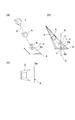
図3は、第2実施形態に係る放射線画像取得装置の正面図である。図3に示す放射線画像取得装置1Aが図1に示した第1実施形態の放射線画像取得装置1と異なる点は、放射線源2が入射面6aの法線B上に配置されている点と、表面検出器3が、入射面6aの法線Bから外れた位置に配置され、波長変換板6と放射線源2との間で法線B(光軸X)上に配置された反射ミラー15を介してシンチレーション光を集光する点である。なお、図3においては、タイミング制御部7、画像処理装置8、及び表示装置9の図示は省略されている。図5~図8においても、同様に、これらの構成の図示は省略されている。
FIG. 3 is a front view of the radiological image acquisition apparatus according to the second embodiment. The radiation image acquisition apparatus 1A shown in FIG. 3 is different from the radiation image acquisition apparatus 1 of the first embodiment shown in FIG. 1 in that the radiation source 2 is arranged on the normal B of the incident surface 6a. The surface detector 3 is disposed at a position deviated from the normal line B of the incident surface 6a, and a reflection mirror 15 disposed on the normal line B (optical axis X) between the wavelength conversion plate 6 and the radiation source 2 is provided. It is a point which condenses scintillation light through. In FIG. 3, the timing control unit 7, the image processing device 8, and the display device 9 are not shown. Similarly, in FIGS. 5 to 8, illustration of these configurations is omitted.
放射線画像取得装置1Aの構成に関し、より具体的には、放射線源2は、放射線の光軸Xが入射面6aの法線Bに一致するように配置されている。また、反射ミラー15は、その反射面15aが法線B方向に対して所定の角度(例えば、45度)をなすように配置されており、入射面6aから法線B方向に出射されたシンチレーション光を法線Bに対して所定の方向に反射する。反射ミラー15としては、例えば放射線を透過する光学ミラーが用いられる。表面検出器3は、内蔵する集光レンズ部3aの光軸および反射面15aのなす角と、法線Bおよび反射面15aのなす角とが等しくなるように配置されている。この集光レンズ部3aは、入射面6aから法線B方向に出射され、反射ミラー15により法線Bに対して所定の方向に反射されたシンチレーション光を撮像部3bに向けて集光する。
Regarding the configuration of the radiation image acquisition apparatus 1A, more specifically, the radiation source 2 is arranged so that the optical axis X of the radiation coincides with the normal B of the incident surface 6a. The reflecting mirror 15 is arranged such that the reflecting surface 15a forms a predetermined angle (for example, 45 degrees) with respect to the normal B direction, and the scintillation emitted from the incident surface 6a in the normal B direction. The light is reflected in a predetermined direction with respect to the normal B. For example, an optical mirror that transmits radiation is used as the reflection mirror 15. The surface detector 3 is arranged so that the angle formed by the optical axis of the built-in condenser lens portion 3a and the reflection surface 15a is equal to the angle formed by the normal B and the reflection surface 15a. The condensing lens unit 3a condenses the scintillation light emitted in the normal B direction from the incident surface 6a and reflected in a predetermined direction with respect to the normal B by the reflecting mirror 15 toward the imaging unit 3b.
上記のようにして、表面検出器3は、放射線源2からの放射線の出射領域(放射線束12が存在する領域)から離れるように配置されている。これにより、放射線源2からの放射線による表面検出器3の被曝が防止され、表面検出器3の内部で放射線の直接変換信号が生じてノイズが発生することが防止されている。また、波長変換板6の入射面6aから表面検出器3までの光路長と、波長変換板6の裏面6bから裏面検出器4までの光路長とは、等しくてもよい。
As described above, the surface detector 3 is arranged so as to be separated from the radiation emission region (region where the radiation bundle 12 exists) from the radiation source 2. As a result, exposure of the surface detector 3 by radiation from the radiation source 2 is prevented, and generation of noise due to generation of a direct radiation conversion signal inside the surface detector 3 is prevented. Further, the optical path length from the incident surface 6 a of the wavelength conversion plate 6 to the front surface detector 3 and the optical path length from the back surface 6 b of the wavelength conversion plate 6 to the back surface detector 4 may be equal.
図4(a)は、放射線画像取得装置1Aにおける放射線源2、対象物A、及び波長変換板6の位置関係を示す斜視図、図4(b)は、放射線源2、対象物A、及び波長変換板6の位置関係を示す正面図、図4(c)は、波長変換板6に投影される対象物Aの投影像Eを示す平面図である。図4では、理解を容易にするために、対象物Aが立方体形状である場合について示している。図4(a)に示すように、放射線源2が入射面6aの法線B上に配置され、放射線の光軸Xが入射面6aの法線Bに一致していると、図4(c)に示すように、入射面6a上への投影像Eにはあおりが生じない。そして、表面検出器3では、投影像Eを反射ミラー15を介して法線B方向から撮像すると共に、裏面検出器4では、投影像Eを法線C方向から撮像するため、画像にはあおりが生じず、画像処理装置8での両画像間における演算が容易になる。また、投影像Eにあおりが無いので、画像処理装置8によるあおり補正は不要になっている。なお、放射線画像取得装置1Aでは、反射ミラー15が放射線源2の光軸X上に配置されているため、反射ミラー15による放射線の吸収が生じる。
4A is a perspective view showing the positional relationship between the radiation source 2, the object A, and the wavelength conversion plate 6 in the radiation image acquisition apparatus 1A, and FIG. 4B is the radiation source 2, the object A, and FIG. 4C is a plan view showing a projection image E of the object A projected onto the wavelength conversion plate 6. FIG. 4 shows a case where the object A has a cubic shape for easy understanding. As shown in FIG. 4A, when the radiation source 2 is disposed on the normal line B of the incident surface 6a and the optical axis X of the radiation coincides with the normal line B of the incident surface 6a, FIG. As shown in FIG. 5A, no tilt occurs in the projected image E on the incident surface 6a. The front surface detector 3 captures the projected image E from the normal B direction via the reflection mirror 15 and the back surface detector 4 captures the projected image E from the normal C direction. Does not occur, and the calculation between the two images in the image processing apparatus 8 is facilitated. Further, since there is no tilt in the projection image E, the tilt correction by the image processing device 8 is not necessary. In the radiographic image acquisition apparatus 1A, the reflection mirror 15 is disposed on the optical axis X of the radiation source 2, so that radiation is absorbed by the reflection mirror 15.
放射線画像取得装置1Aによれば、放射線画像取得装置1と同様の作用効果が奏される。また、放射線源2が入射面6aの法線B上に配置されるため、波長変換板6への投影像Eにあおりが生じず、投影像Eのあおりを補正するための演算が不要になっている。さらには、放射線による表面検出器3の被曝が防止され、表面検出器3の内部におけるノイズの発生が防止される。
According to the radiological image acquisition apparatus 1A, the same effects as the radiological image acquisition apparatus 1 can be obtained. Further, since the radiation source 2 is arranged on the normal line B of the incident surface 6a, no distortion occurs in the projection image E onto the wavelength conversion plate 6, and an operation for correcting the inclination of the projection image E becomes unnecessary. ing. Furthermore, exposure of the surface detector 3 due to radiation is prevented, and generation of noise inside the surface detector 3 is prevented.
図5は、第3実施形態に係る放射線画像取得装置の正面図である。図5に示す放射線画像取得装置1Bが図1に示した第1実施形態の放射線画像取得装置1と異なる点は、裏面検出器4が、裏面6bの法線Cから外れた位置に配置され、法線C上に配置された反射ミラー16を介してシンチレーション光を集光する点である。より具体的には、反射ミラー16は、その反射面16aが法線C方向に対して所定の角度(例えば、45度)をなすように配置されており、裏面6bから法線C方向に出射されたシンチレーション光を法線Cに対して所定の方向に反射する。反射ミラー16としては、例えば光学ミラーや又はプリズムが用いられる。裏面検出器4は、内蔵する集光レンズ部4aの光軸および反射面16aのなす角と、法線Cおよび反射面16aのなす角とが等しくなるように配置されている。この集光レンズ部4aは、裏面6bから法線C方向に出射され、反射ミラー16により法線Cに対して所定の方向に反射されたシンチレーション光を撮像部4bに向けて集光する。
FIG. 5 is a front view of the radiation image acquisition apparatus according to the third embodiment. The radiological image acquisition apparatus 1B shown in FIG. 5 is different from the radiological image acquisition apparatus 1 of the first embodiment shown in FIG. This is a point where the scintillation light is collected through the reflection mirror 16 arranged on the normal line C. More specifically, the reflecting mirror 16 is disposed such that the reflecting surface 16a forms a predetermined angle (for example, 45 degrees) with respect to the normal C direction, and is emitted from the back surface 6b in the normal C direction. The scintillation light thus reflected is reflected in a predetermined direction with respect to the normal C. As the reflection mirror 16, for example, an optical mirror or a prism is used. The back surface detector 4 is arranged so that the angle formed by the optical axis of the built-in condenser lens portion 4a and the reflection surface 16a is equal to the angle formed by the normal C and the reflection surface 16a. The condensing lens unit 4a collects the scintillation light emitted from the back surface 6b in the normal C direction and reflected by the reflecting mirror 16 in the predetermined direction with respect to the normal C toward the imaging unit 4b.
上記のようにして、裏面検出器4は、放射線源2からの放射線の出射領域(放射線束12が存在する領域)から離れるように配置されている。これにより、放射線源2からの放射線による裏面検出器4の被曝が防止され、裏面検出器4の内部で放射線の直接変換信号が生じてノイズが発生することが防止されている。また、波長変換板6の入射面6aから表面検出器3までの光路長と、波長変換板6の裏面6bから裏面検出器4までの光路長とは、等しくてもよい。
As described above, the back surface detector 4 is arranged so as to be separated from the radiation emission region (region where the radiation bundle 12 exists) from the radiation source 2. As a result, exposure of the back surface detector 4 due to radiation from the radiation source 2 is prevented, and noise is prevented from being generated due to the direct conversion signal of radiation inside the back surface detector 4. Further, the optical path length from the incident surface 6 a of the wavelength conversion plate 6 to the front surface detector 3 and the optical path length from the back surface 6 b of the wavelength conversion plate 6 to the back surface detector 4 may be equal.
放射線画像取得装置1Bによれば、放射線画像取得装置1,1Aと同様の作用効果が奏される。また、放射線による裏面検出器4の被曝が防止され、裏面検出器4の内部におけるノイズの発生が防止される。さらには、波長変換板6からの表面検出器3および裏面検出器4までの光路長を調整することができ、第1および第2の撮像手段の位置合わせが容易になる。その結果として、第1および第2の撮像手段の撮像条件(撮像タイミングの同時性や撮像位置の同一性など)を合せやすくなる。
According to the radiation image acquisition apparatus 1B, the same effects as the radiation image acquisition apparatuses 1 and 1A are exhibited. Further, exposure of the back surface detector 4 due to radiation is prevented, and generation of noise inside the back surface detector 4 is prevented. Furthermore, the optical path lengths from the wavelength conversion plate 6 to the front surface detector 3 and the back surface detector 4 can be adjusted, and the first and second imaging means can be easily aligned. As a result, it becomes easy to match the imaging conditions (simultaneity of imaging timing, identity of imaging position, etc.) of the first and second imaging means.
図6は、第4実施形態に係る放射線画像取得装置の正面図である。図6に示す放射線画像取得装置1Cが図1に示した第1実施形態の放射線画像取得装置1と異なる点は、裏面6bと裏面検出器4との間で裏面6bに対面させてテーパファイバ17が配置されている点である。より具体的には、テーパファイバ17は、その軸線が裏面6bの法線Cに一致するように配置されており、裏面6bから法線C方向に出射されたシンチレーション光を裏面検出器4の集光レンズ部に導光する。このテーパファイバ17と裏面検出器4とによって、ファイバカップリング検出器18が構成されている。
FIG. 6 is a front view of the radiation image acquisition apparatus according to the fourth embodiment. The radiographic image acquisition apparatus 1C shown in FIG. 6 is different from the radiographic image acquisition apparatus 1 of the first embodiment shown in FIG. 1 in that the taper fiber 17 faces the back surface 6b between the back surface 6b and the back surface detector 4. Is the point where is placed. More specifically, the taper fiber 17 is arranged so that the axis thereof coincides with the normal line C of the back surface 6b, and scintillation light emitted from the back surface 6b in the normal C direction is collected by the back surface detector 4. The light is guided to the optical lens unit. The tapered fiber 17 and the back surface detector 4 constitute a fiber coupling detector 18.
放射線画像取得装置1Cによれば、放射線画像取得装置1,1A,1Bと同様の作用効果が奏される。また、テーパファイバ17によって裏面6b側のシンチレーション光が高い集光効率で集光される。通常、波長変換板6の裏面6b側の蛍光象は暗くなりがちであるが、ファイバカップリング検出器18を採用することで光学系のロスを減らすことが可能になっている。さらには、テーパファイバ17によって放射線源2からの放射線が遮断され、裏面検出器4の被爆が防止される。
According to the radiation image acquisition device 1C, the same effects as the radiation image acquisition devices 1, 1A, 1B are exhibited. Further, the scintillation light on the back surface 6b side is condensed with high condensing efficiency by the taper fiber 17. Usually, the fluorescent image on the back surface 6b side of the wavelength conversion plate 6 tends to be dark, but by adopting the fiber coupling detector 18, the loss of the optical system can be reduced. Furthermore, radiation from the radiation source 2 is blocked by the taper fiber 17 and the back surface detector 4 is prevented from being exposed.
以上、本発明の実施形態について説明したが、本発明は上記実施形態に限られるものではない。例えば、放射線源2が入射面6aの法線B上に配置される場合において、図7に示す各種の変形態様を採ることもできる。すなわち、図7(a)に示すように、入射面6a側に反射ミラー15を配置すると共に、裏面6b側に反射ミラー16を配置した放射線画像取得装置1Dとすることもできる。また、図7(b)に示すように、入射面6a側に反射ミラー15を配置すると共に、裏面6b側にファイバカップリング検出器18を配置した放射線画像取得装置1Eとすることもできる。
As mentioned above, although embodiment of this invention was described, this invention is not limited to the said embodiment. For example, when the radiation source 2 is disposed on the normal B of the incident surface 6a, various modifications shown in FIG. 7 can be employed. That is, as shown to Fig.7 (a), while setting the reflective mirror 15 in the entrance plane 6a side, it can also be set as the radiographic image acquisition apparatus 1D which has arrange | positioned the reflective mirror 16 in the back surface 6b side. Further, as shown in FIG. 7B, the radiation image acquisition apparatus 1E in which the reflection mirror 15 is disposed on the incident surface 6a side and the fiber coupling detector 18 is disposed on the back surface 6b side can be provided.
さらには、放射線源2が入射面6aの法線Bから外れた位置に配置される場合において、図8に示す各種の変形態様を採ることもできる。すなわち、図8(a)に示すように、入射面6a側に反射ミラー15を配置すると共に、裏面6bの法線C上に裏面検出器4を配置した放射線画像取得装置1Fとすることもできる。また、図8(b)に示すように、入射面6a側に反射ミラー15を配置すると共に、裏面6b側に反射ミラー16を配置した放射線画像取得装置1Gとすることもできる。さらには、図8(c)に示すように、入射面6a側に反射ミラー15を配置すると共に、裏面6b側にファイバカップリング検出器18を配置した放射線画像取得装置1Hとすることもできる。
Furthermore, when the radiation source 2 is disposed at a position deviating from the normal line B of the incident surface 6a, various modifications shown in FIG. 8 can be adopted. That is, as shown to Fig.8 (a), while setting the reflective mirror 15 to the entrance plane 6a side, it can also be set as the radiographic image acquisition apparatus 1F which has arrange | positioned the back surface detector 4 on the normal line C of the back surface 6b. . Further, as shown in FIG. 8B, the radiation image acquisition apparatus 1G in which the reflection mirror 15 is disposed on the incident surface 6a side and the reflection mirror 16 is disposed on the back surface 6b side can also be provided. Further, as shown in FIG. 8C, the radiation image acquisition apparatus 1H in which the reflection mirror 15 is disposed on the incident surface 6a side and the fiber coupling detector 18 is disposed on the back surface 6b side may be provided.
また、上記実施形態では、反射ミラー15,16を用いる場合、反射ミラー15,16が法線B,Cに対して45度をなすように配置され、集光レンズ部3a,4aの光軸が法線B,Cに対して直交する場合について説明したが、このような配置に限られず、反射ミラー15,16の角度や表面検出器3および裏面検出器4の配置は、装置内のレイアウトに応じて適宜変更することができる。
Moreover, in the said embodiment, when using the reflective mirrors 15 and 16, the reflective mirrors 15 and 16 are arrange | positioned so that it may make 45 degree | times with respect to normal B, C, and the optical axis of the condensing lens part 3a, 4a is set. Although the case where the normal lines B and C are orthogonal to each other has been described, the present invention is not limited to such an arrangement, and the angles of the reflection mirrors 15 and 16 and the arrangement of the front surface detector 3 and the rear surface detector 4 depend on the layout in the apparatus. It can be changed accordingly.
また、上記実施形態では、任意の点γおよび任意の点αが入射面6a上で一致している場合について説明したが、これらは入射面6a上の異なる位置にあっても良い。この場合、光軸Xが入射面6aに対して直交するように放射線源2を配置すると共に、集光レンズ部3aの光軸が入射面6aに対して直交するように表面検出器3を配置することができる。すなわち、放射線源2の光軸Xおよび集光レンズ部3aの光軸は互いに平行となり、これらの光軸同士の離間距離は、点γおよび点αの離間距離に等しくなる。このような構成においても、表面検出器3によって、入射面6aの法線方向に出射されるシンチレーション光を集光して撮像することができる。
In the above embodiment, the case where the arbitrary point γ and the arbitrary point α coincide with each other on the incident surface 6a has been described, but these may be at different positions on the incident surface 6a. In this case, the radiation source 2 is arranged so that the optical axis X is orthogonal to the incident surface 6a, and the surface detector 3 is arranged so that the optical axis of the condenser lens portion 3a is orthogonal to the incident surface 6a. can do. That is, the optical axis X of the radiation source 2 and the optical axis of the condensing lens unit 3a are parallel to each other, and the distance between these optical axes is equal to the distance between the points γ and α. Even in such a configuration, the surface detector 3 can collect and image scintillation light emitted in the normal direction of the incident surface 6a.
また、上記実施形態では、検出器としてレンズカップリング型の検出器を用いたが、集光レンズ部と撮像部とをそれぞれ別体として備えてもよい。
In the above embodiment, the lens coupling type detector is used as the detector. However, the condenser lens unit and the imaging unit may be provided separately.
また、対象物Aを半導体デバイスとし、その半導体デバイスを検査対象とする半導体故障検査装置として上記実施形態の放射線画像取得装置を適用すると有効である。この場合、検査対象となる半導体デバイスを透過した放射線が撮像部(画像取得用の撮像素子)によりカットされることがないため、半導体デバイスの故障などを精度良く検出することができる。
It is also effective to apply the radiation image acquisition apparatus of the above embodiment as a semiconductor fault inspection apparatus in which the object A is a semiconductor device and the semiconductor device is an inspection target. In this case, since the radiation that has passed through the semiconductor device to be inspected is not cut by the imaging unit (image acquisition device for image acquisition), a failure of the semiconductor device can be detected with high accuracy.
本発明の一形態によれば、異なるエネルギー帯の放射線画像を取得することができ、かつ、対象物を透過した放射線に与える影響を低減することができる。
According to one aspect of the present invention, radiation images in different energy bands can be acquired, and the influence on radiation transmitted through the object can be reduced.
1,1A~1H…放射線画像取得装置、2…放射線源、3…表面観察用光検出器(第1の撮像手段)、3a…集光レンズ部、3b…撮像部、4…裏面観察用光検出器(第2の撮像手段)、4a…集光レンズ部、4b…撮像部、6…波長変換板(波長変換部材)、6a…入射面、6b…裏面(反対側の面)、15…反射ミラー、16…反射ミラー、17…テーパファイバ、A…対象物、B…入射面の法線、C…裏面の法線。
DESCRIPTION OF SYMBOLS 1,1A-1H ... Radiation image acquisition apparatus, 2 ... Radiation source, 3 ... Surface detector (1st imaging means), 3a ... Condensing lens part, 3b ... Imaging part, 4 ... Back surface observation light Detector (second imaging means), 4a ... condensing lens unit, 4b ... imaging unit, 6 ... wavelength conversion plate (wavelength conversion member), 6a ... incident surface, 6b ... back surface (opposite surface), 15 ... Reflecting mirror, 16 ... reflecting mirror, 17 ... tapered fiber, A ... object, B ... normality of incident surface, C ... normality of back surface.
Claims (7)
- 放射線を出射する放射線源と、
前記放射線源から出射され、対象物を透過した前記放射線の入射に応じてシンチレーション光を発生させる平板状の波長変換部材と、
前記波長変換部材の前記放射線の入射面から前記入射面の法線方向に出射されるシンチレーション光を集光して撮像する第1の撮像手段と、
前記波長変換部材の前記入射面とは反対側の面から前記反対側の面の法線方向に出射されるシンチレーション光を集光して撮像する第2の撮像手段と、
を備えることを特徴とする放射線画像取得装置。 A radiation source that emits radiation; and
A flat wavelength conversion member that generates scintillation light in response to the incidence of the radiation emitted from the radiation source and transmitted through the object;
First imaging means for collecting and imaging scintillation light emitted in the normal direction of the incident surface from the radiation incident surface of the wavelength conversion member;
Second imaging means for collecting and imaging scintillation light emitted in a normal direction of the opposite surface from a surface opposite to the incident surface of the wavelength conversion member;
A radiological image acquisition apparatus comprising: - 前記第1の撮像手段および前記第2の撮像手段のそれぞれは、
前記波長変換部材から出射される前記シンチレーション光を集光する集光レンズ部と、
集光された前記シンチレーション光を撮像する撮像部と、
を有することを特徴とする請求項1記載の放射線画像取得装置。 Each of the first imaging means and the second imaging means
A condensing lens part that condenses the scintillation light emitted from the wavelength conversion member;
An imaging unit for imaging the collected scintillation light;
The radiological image acquisition apparatus according to claim 1, comprising: - 前記放射線源は、前記放射線源の光軸と前記入射面とのなす角度が0度より大きく90度より小さくなるように配置されると共に、
前記第1の撮像手段は、前記入射面の法線上に配置される
ことを特徴とする請求項1又は2記載の放射線画像取得装置。 The radiation source is arranged such that an angle formed by the optical axis of the radiation source and the incident surface is greater than 0 degree and less than 90 degrees,
The radiographic image acquisition apparatus according to claim 1, wherein the first imaging unit is disposed on a normal line of the incident surface. - 前記放射線源は、前記入射面の法線上に配置されると共に、
前記第1の撮像手段は、前記入射面の法線から外れた位置に配置され、前記波長変換部材と前記放射線源との間に配置された反射ミラーを介して前記シンチレーション光を集光する
ことを特徴とする請求項1又は2記載の放射線画像取得装置。 The radiation source is disposed on a normal line of the incident surface;
The first imaging unit is disposed at a position deviating from the normal line of the incident surface, and condenses the scintillation light via a reflection mirror disposed between the wavelength conversion member and the radiation source. The radiographic image acquisition device according to claim 1 or 2. - 前記第2の撮像手段は、前記反対側の面の法線から外れた位置に配置され、前記反対側の面の法線上に配置された反射ミラーを介して前記シンチレーション光を集光する
ことを特徴とする請求項1~4のいずれか1項に記載の放射線画像取得装置。 The second imaging means is disposed at a position deviating from the normal line of the opposite surface, and condenses the scintillation light via a reflection mirror disposed on the normal line of the opposite surface. The radiological image acquisition apparatus according to any one of claims 1 to 4, characterized in that: - 前記波長変換部材の前記反対側の面と前記第2の撮像手段との間には、前記反対側の面に対面させてテーパファイバが配置されている
ことを特徴とする請求項1~4のいずれか1項に記載の放射線画像取得装置。 The taper fiber is disposed between the opposite surface of the wavelength conversion member and the second imaging unit so as to face the opposite surface. The radiographic image acquisition apparatus of any one of Claims. - 前記対象物は半導体デバイスであり、
当該半導体デバイスを検査対象とする半導体故障検査装置に適用される
ことを特徴とする請求項1~6のいずれか1項に記載の放射線画像取得装置。 The object is a semiconductor device;
7. The radiological image acquisition apparatus according to claim 1, wherein the radiological image acquisition apparatus is applied to a semiconductor fault inspection apparatus that inspects the semiconductor device.
Priority Applications (5)
| Application Number | Priority Date | Filing Date | Title |
|---|---|---|---|
| US13/981,469 US9279890B2 (en) | 2011-01-25 | 2011-10-21 | Radiation image acquisition device |
| CN201190001001.8U CN203616268U (en) | 2011-01-25 | 2011-10-21 | Radioactive ray image obtaining device |
| ES11857086T ES2787256T3 (en) | 2011-01-25 | 2011-10-21 | Radiation imaging device |
| DK11857086.0T DK2669665T3 (en) | 2011-01-25 | 2011-10-21 | RADIATION IMAGE CATCHING DEVICE |
| EP11857086.0A EP2669665B1 (en) | 2011-01-25 | 2011-10-21 | Radiation image acquisition device |
Applications Claiming Priority (2)
| Application Number | Priority Date | Filing Date | Title |
|---|---|---|---|
| JP2011-013192 | 2011-01-25 | ||
| JP2011013192A JP5784916B2 (en) | 2011-01-25 | 2011-01-25 | Radiation image acquisition device |
Publications (1)
| Publication Number | Publication Date |
|---|---|
| WO2012101879A1 true WO2012101879A1 (en) | 2012-08-02 |
Family
ID=46580466
Family Applications (1)
| Application Number | Title | Priority Date | Filing Date |
|---|---|---|---|
| PCT/JP2011/074327 WO2012101879A1 (en) | 2011-01-25 | 2011-10-21 | Radiation image acquisition device |
Country Status (8)
| Country | Link |
|---|---|
| US (1) | US9279890B2 (en) |
| EP (1) | EP2669665B1 (en) |
| JP (1) | JP5784916B2 (en) |
| CN (1) | CN203616268U (en) |
| DE (1) | DE202011110808U1 (en) |
| DK (1) | DK2669665T3 (en) |
| ES (1) | ES2787256T3 (en) |
| WO (1) | WO2012101879A1 (en) |
Cited By (3)
| Publication number | Priority date | Publication date | Assignee | Title |
|---|---|---|---|---|
| WO2014013829A1 (en) * | 2012-07-20 | 2014-01-23 | 浜松ホトニクス株式会社 | Radiation image acquisition device |
| JPWO2017056680A1 (en) * | 2015-09-30 | 2018-07-19 | 浜松ホトニクス株式会社 | Radiation image acquisition system and radiation image acquisition method |
| US10101469B2 (en) | 2011-01-25 | 2018-10-16 | Hamamatsu Photonics K.K. | Radiation image acquisition device |
Families Citing this family (7)
| Publication number | Priority date | Publication date | Assignee | Title |
|---|---|---|---|---|
| EP2919037A1 (en) * | 2014-03-13 | 2015-09-16 | Université de Technologie de Troyes | Method for optimising the collection of photons in scintillator crystals, crystal and uses thereof |
| EP3163717B1 (en) * | 2014-06-24 | 2024-04-03 | Kubota Corporation | Stator of electric motor and cooling structure for dynamo-electric machine |
| CN104155681A (en) * | 2014-07-21 | 2014-11-19 | 北京辛耕普华医疗科技有限公司 | Locator and method for monitoring radioactive source |
| WO2018060325A1 (en) | 2016-09-29 | 2018-04-05 | Marel Iceland Ehf. | A method of generating a three dimensional surface profile of a food object |
| KR102592905B1 (en) * | 2016-12-21 | 2023-10-23 | 삼성전자주식회사 | X-ray image capturing apparatus and controlling method thereof |
| DK3690429T3 (en) * | 2019-02-04 | 2021-12-13 | Microtec Srl | Tunnel ct scanner |
| JPWO2022113507A1 (en) | 2020-11-25 | 2022-06-02 |
Citations (4)
| Publication number | Priority date | Publication date | Assignee | Title |
|---|---|---|---|---|
| JPH0727866A (en) | 1993-07-14 | 1995-01-31 | Fuji Photo Film Co Ltd | Radiation detector |
| JP2000510729A (en) * | 1996-05-13 | 2000-08-22 | ユニバーシテイ・オブ・マサチユセツツ・メデイカル・センター | System for quantitative radiation imaging |
| JP2005207827A (en) * | 2004-01-21 | 2005-08-04 | Nagoya Electric Works Co Ltd | X-ray inspection device and method, and control program of x-ray inspection device |
| JP2007155653A (en) * | 2005-12-08 | 2007-06-21 | Olympus Corp | Radiation observation apparatus |
Family Cites Families (11)
| Publication number | Priority date | Publication date | Assignee | Title |
|---|---|---|---|---|
| US4578803A (en) * | 1981-12-07 | 1986-03-25 | Albert Macovski | Energy-selective x-ray recording and readout system |
| JPH0795100B2 (en) | 1986-09-24 | 1995-10-11 | 株式会社日立メデイコ | X-ray baggage inspection device |
| JPH05152391A (en) * | 1991-12-02 | 1993-06-18 | Fujitsu Ltd | X-ray test device |
| JPH05312734A (en) * | 1992-05-11 | 1993-11-22 | Fujitsu Ltd | X-ray detection |
| JPH0861941A (en) * | 1994-08-23 | 1996-03-08 | Toshiba Corp | Radiation inspecting device |
| JP2000298198A (en) | 1999-02-08 | 2000-10-24 | Fuji Photo Film Co Ltd | Method and device for acquiring radiograph data |
| JP2001004561A (en) * | 1999-06-17 | 2001-01-12 | On Denshi Kk | Board inspecting device |
| US7130375B1 (en) * | 2004-01-14 | 2006-10-31 | Xradia, Inc. | High resolution direct-projection type x-ray microtomography system using synchrotron or laboratory-based x-ray source |
| US7405406B1 (en) | 2006-04-21 | 2008-07-29 | Radiation Monitoring Devices, Inc. | Two-sided scintillation detectors and related methods |
| JP4853964B2 (en) * | 2006-12-28 | 2012-01-11 | 株式会社Ihi検査計測 | X-ray sensor for X-ray inspection equipment |
| JP2007327967A (en) * | 2007-07-30 | 2007-12-20 | Toshiba Corp | Radiation discrimination measuring device |
-
2011
- 2011-01-25 JP JP2011013192A patent/JP5784916B2/en active Active
- 2011-10-21 CN CN201190001001.8U patent/CN203616268U/en not_active Expired - Lifetime
- 2011-10-21 DE DE202011110808.6U patent/DE202011110808U1/en not_active Expired - Lifetime
- 2011-10-21 WO PCT/JP2011/074327 patent/WO2012101879A1/en active Application Filing
- 2011-10-21 US US13/981,469 patent/US9279890B2/en active Active
- 2011-10-21 ES ES11857086T patent/ES2787256T3/en active Active
- 2011-10-21 DK DK11857086.0T patent/DK2669665T3/en active
- 2011-10-21 EP EP11857086.0A patent/EP2669665B1/en active Active
Patent Citations (4)
| Publication number | Priority date | Publication date | Assignee | Title |
|---|---|---|---|---|
| JPH0727866A (en) | 1993-07-14 | 1995-01-31 | Fuji Photo Film Co Ltd | Radiation detector |
| JP2000510729A (en) * | 1996-05-13 | 2000-08-22 | ユニバーシテイ・オブ・マサチユセツツ・メデイカル・センター | System for quantitative radiation imaging |
| JP2005207827A (en) * | 2004-01-21 | 2005-08-04 | Nagoya Electric Works Co Ltd | X-ray inspection device and method, and control program of x-ray inspection device |
| JP2007155653A (en) * | 2005-12-08 | 2007-06-21 | Olympus Corp | Radiation observation apparatus |
Cited By (9)
| Publication number | Priority date | Publication date | Assignee | Title |
|---|---|---|---|---|
| US10101469B2 (en) | 2011-01-25 | 2018-10-16 | Hamamatsu Photonics K.K. | Radiation image acquisition device |
| US10746884B2 (en) | 2011-01-25 | 2020-08-18 | Hamamatsu Photonics K.K. | Radiation image acquisition device |
| WO2014013829A1 (en) * | 2012-07-20 | 2014-01-23 | 浜松ホトニクス株式会社 | Radiation image acquisition device |
| JP2014021015A (en) * | 2012-07-20 | 2014-02-03 | Hamamatsu Photonics Kk | Radiographic image acquisition device |
| US9500600B2 (en) | 2012-07-20 | 2016-11-22 | Hamamatsu Photonics K.K. | Radiation image acquisition system |
| US10234406B2 (en) | 2012-07-20 | 2019-03-19 | Hamamatsu Photonics K.K. | Radiation image acquisition system |
| JPWO2017056680A1 (en) * | 2015-09-30 | 2018-07-19 | 浜松ホトニクス株式会社 | Radiation image acquisition system and radiation image acquisition method |
| US10859715B2 (en) | 2015-09-30 | 2020-12-08 | Hamamatsu Photonics K.K. | Radiation image acquisition system and radiation image acquisition method |
| US11237278B2 (en) | 2015-09-30 | 2022-02-01 | Hamamatsu Photonics K.K. | Radiation image acquisition system and radiation image acquisition method |
Also Published As
| Publication number | Publication date |
|---|---|
| CN203616268U (en) | 2014-05-28 |
| ES2787256T3 (en) | 2020-10-15 |
| JP5784916B2 (en) | 2015-09-24 |
| EP2669665B1 (en) | 2020-04-01 |
| DE202011110808U1 (en) | 2016-07-14 |
| EP2669665A4 (en) | 2017-04-19 |
| US20140016753A1 (en) | 2014-01-16 |
| EP2669665A1 (en) | 2013-12-04 |
| US9279890B2 (en) | 2016-03-08 |
| JP2012154733A (en) | 2012-08-16 |
| DK2669665T3 (en) | 2020-06-02 |
Similar Documents
| Publication | Publication Date | Title |
|---|---|---|
| JP5784916B2 (en) | Radiation image acquisition device | |
| JP5792472B2 (en) | Radiation image acquisition device | |
| JP5890099B2 (en) | Radiation image acquisition device | |
| JP5944254B2 (en) | Radiation image acquisition device | |
| US8829449B2 (en) | Scintillator plate | |
| JP3204649U (en) | Radiation image acquisition device and imaging unit | |
| JP5973040B2 (en) | Radiation image acquisition device | |
| JP6671413B2 (en) | Radiation image acquisition device | |
| JP5706387B2 (en) | Scintillator plate and image acquisition device | |
| WO2022113507A1 (en) | Imaging unit and imaging system | |
| JP6345720B2 (en) | Radiation image acquisition device and method for adjusting radiation image acquisition device |
Legal Events
| Date | Code | Title | Description |
|---|---|---|---|
| WWE | Wipo information: entry into national phase |
Ref document number: 201190001001.8 Country of ref document: CN |
|
| 121 | Ep: the epo has been informed by wipo that ep was designated in this application |
Ref document number: 11857086 Country of ref document: EP Kind code of ref document: A1 |
|
| NENP | Non-entry into the national phase |
Ref country code: DE |
|
| WWE | Wipo information: entry into national phase |
Ref document number: 2011857086 Country of ref document: EP |
|
| WWE | Wipo information: entry into national phase |
Ref document number: 13981469 Country of ref document: US |