WO2022113507A1 - Imaging unit and imaging system - Google Patents
Imaging unit and imaging system Download PDFInfo
- Publication number
- WO2022113507A1 WO2022113507A1 PCT/JP2021/035165 JP2021035165W WO2022113507A1 WO 2022113507 A1 WO2022113507 A1 WO 2022113507A1 JP 2021035165 W JP2021035165 W JP 2021035165W WO 2022113507 A1 WO2022113507 A1 WO 2022113507A1
- Authority
- WO
- WIPO (PCT)
- Prior art keywords
- sensor module
- lens
- scintillator
- scintillation light
- radiation
- Prior art date
Links
- 238000003384 imaging method Methods 0.000 title claims abstract description 64
- 238000012545 processing Methods 0.000 claims abstract description 75
- 230000005855 radiation Effects 0.000 claims description 76
- 230000032258 transport Effects 0.000 claims description 57
- 238000001514 detection method Methods 0.000 claims description 11
- 230000003287 optical effect Effects 0.000 description 34
- 230000000007 visual effect Effects 0.000 description 9
- 238000010586 diagram Methods 0.000 description 8
- 239000000758 substrate Substances 0.000 description 8
- 238000012546 transfer Methods 0.000 description 5
- XEEYBQQBJWHFJM-UHFFFAOYSA-N Iron Chemical compound [Fe] XEEYBQQBJWHFJM-UHFFFAOYSA-N 0.000 description 4
- 238000012937 correction Methods 0.000 description 4
- 239000000463 material Substances 0.000 description 4
- 229910052751 metal Inorganic materials 0.000 description 4
- 239000002184 metal Substances 0.000 description 4
- 230000009977 dual effect Effects 0.000 description 3
- 238000007689 inspection Methods 0.000 description 3
- 230000010354 integration Effects 0.000 description 3
- 230000001681 protective effect Effects 0.000 description 3
- 239000000126 substance Substances 0.000 description 3
- 229910052684 Cerium Inorganic materials 0.000 description 2
- 230000001154 acute effect Effects 0.000 description 2
- 230000008878 coupling Effects 0.000 description 2
- 238000010168 coupling process Methods 0.000 description 2
- 238000005859 coupling reaction Methods 0.000 description 2
- 230000004907 flux Effects 0.000 description 2
- 235000013305 food Nutrition 0.000 description 2
- 239000011521 glass Substances 0.000 description 2
- 238000003702 image correction Methods 0.000 description 2
- 229910052742 iron Inorganic materials 0.000 description 2
- 229910001220 stainless steel Inorganic materials 0.000 description 2
- 239000010935 stainless steel Substances 0.000 description 2
- PXFBZOLANLWPMH-UHFFFAOYSA-N 16-Epiaffinine Natural products C1C(C2=CC=CC=C2N2)=C2C(=O)CC2C(=CC)CN(C)C1C2CO PXFBZOLANLWPMH-UHFFFAOYSA-N 0.000 description 1
- RYGMFSIKBFXOCR-UHFFFAOYSA-N Copper Chemical compound [Cu] RYGMFSIKBFXOCR-UHFFFAOYSA-N 0.000 description 1
- 229910052688 Gadolinium Inorganic materials 0.000 description 1
- 241000238631 Hexapoda Species 0.000 description 1
- 229910052771 Terbium Inorganic materials 0.000 description 1
- 229910052782 aluminium Inorganic materials 0.000 description 1
- XAGFODPZIPBFFR-UHFFFAOYSA-N aluminium Chemical compound [Al] XAGFODPZIPBFFR-UHFFFAOYSA-N 0.000 description 1
- 230000002146 bilateral effect Effects 0.000 description 1
- 210000000988 bone and bone Anatomy 0.000 description 1
- 238000006243 chemical reaction Methods 0.000 description 1
- 229910052802 copper Inorganic materials 0.000 description 1
- 239000010949 copper Substances 0.000 description 1
- 238000007599 discharging Methods 0.000 description 1
- 239000010794 food waste Substances 0.000 description 1
- 239000011133 lead Substances 0.000 description 1
- 235000013372 meat Nutrition 0.000 description 1
- 238000000034 method Methods 0.000 description 1
- 230000004048 modification Effects 0.000 description 1
- 238000012986 modification Methods 0.000 description 1
- 239000011295 pitch Substances 0.000 description 1
- 230000002194 synthesizing effect Effects 0.000 description 1
- 230000009466 transformation Effects 0.000 description 1
- WFKWXMTUELFFGS-UHFFFAOYSA-N tungsten Chemical compound [W] WFKWXMTUELFFGS-UHFFFAOYSA-N 0.000 description 1
- 229910052721 tungsten Inorganic materials 0.000 description 1
- 239000010937 tungsten Substances 0.000 description 1
- 125000000391 vinyl group Chemical group [H]C([*])=C([H])[H] 0.000 description 1
- 229920002554 vinyl polymer Polymers 0.000 description 1
Images


Classifications
-
- G—PHYSICS
- G01—MEASURING; TESTING
- G01T—MEASUREMENT OF NUCLEAR OR X-RADIATION
- G01T1/00—Measuring X-radiation, gamma radiation, corpuscular radiation, or cosmic radiation
- G01T1/16—Measuring radiation intensity
- G01T1/20—Measuring radiation intensity with scintillation detectors
- G01T1/2002—Optical details, e.g. reflecting or diffusing layers
-
- G—PHYSICS
- G01—MEASURING; TESTING
- G01N—INVESTIGATING OR ANALYSING MATERIALS BY DETERMINING THEIR CHEMICAL OR PHYSICAL PROPERTIES
- G01N23/00—Investigating or analysing materials by the use of wave or particle radiation, e.g. X-rays or neutrons, not covered by groups G01N3/00 – G01N17/00, G01N21/00 or G01N22/00
- G01N23/02—Investigating or analysing materials by the use of wave or particle radiation, e.g. X-rays or neutrons, not covered by groups G01N3/00 – G01N17/00, G01N21/00 or G01N22/00 by transmitting the radiation through the material
- G01N23/04—Investigating or analysing materials by the use of wave or particle radiation, e.g. X-rays or neutrons, not covered by groups G01N3/00 – G01N17/00, G01N21/00 or G01N22/00 by transmitting the radiation through the material and forming images of the material
-
- G—PHYSICS
- G01—MEASURING; TESTING
- G01T—MEASUREMENT OF NUCLEAR OR X-RADIATION
- G01T1/00—Measuring X-radiation, gamma radiation, corpuscular radiation, or cosmic radiation
- G01T1/16—Measuring radiation intensity
- G01T1/20—Measuring radiation intensity with scintillation detectors
- G01T1/2018—Scintillation-photodiode combinations
- G01T1/20187—Position of the scintillator with respect to the photodiode, e.g. photodiode surrounding the crystal, the crystal surrounding the photodiode, shape or size of the scintillator
-
- G—PHYSICS
- G01—MEASURING; TESTING
- G01T—MEASUREMENT OF NUCLEAR OR X-RADIATION
- G01T1/00—Measuring X-radiation, gamma radiation, corpuscular radiation, or cosmic radiation
- G01T1/16—Measuring radiation intensity
- G01T1/20—Measuring radiation intensity with scintillation detectors
- G01T1/2018—Scintillation-photodiode combinations
- G01T1/20188—Auxiliary details, e.g. casings or cooling
-
- G06T5/92—
-
- G—PHYSICS
- G06—COMPUTING; CALCULATING OR COUNTING
- G06T—IMAGE DATA PROCESSING OR GENERATION, IN GENERAL
- G06T2207/00—Indexing scheme for image analysis or image enhancement
- G06T2207/10—Image acquisition modality
- G06T2207/10116—X-ray image
Definitions
- This disclosure relates to an imaging unit and an imaging system.
- This conventional imaging system includes a first sensor module and a second sensor module that detect scintillation light emitted from a scintillator.
- the first sensor module and the second sensor module capture images of scintillation light emitted from the front surface and the back surface of the scintillator, respectively.
- dual energy imaging that acquires radiographic images of objects in different energy bands is realized.
- the configuration of the image pickup unit constituting the image pickup system becomes complicated. Further, in an imaging system as described above, there may be restrictions on the arrangement of scintillators in optimizing the imaging of an object. In that case, it is required to secure the degree of freedom in adjusting the imaging position in the imaging unit.
- An object of the present disclosure is to provide an imaging unit and an imaging system that can secure the degree of freedom in adjusting the imaging position with a simple configuration.
- the image pickup unit includes a first sensor module, a second sensor module, a processing board, a first connection member, and a second connection member.
- the first sensor module detects the first lens that collects the first scintillation light and the first scintillation light that is collected by the first lens, and outputs the first image signal corresponding to the detection result.
- the second sensor module detects the second lens that collects the second scintillation light and the second scintillation light that is collected by the second lens, and outputs the second image signal corresponding to the detection result.
- the processing board executes image processing based on the first image signal and the second image signal.
- the first connecting member electrically connects the first sensor module and the processing board and has flexibility.
- the second connecting member electrically connects the second sensor module and the processing board and has flexibility.
- a processing board for processing the first image signal and the second image signal from the first sensor module and the second sensor module is shared. Therefore, the configuration can be simplified as compared with the configuration in which the processing board is provided for each sensor module. Further, in this image pickup unit, each of the first connecting member and the second connecting member connecting the first sensor module and the second sensor module to the processing board has flexibility when the processing board is standardized. Therefore, the imaging positions of the first sensor module and the second sensor module can be adjusted separately. Therefore, a sufficient degree of freedom in adjusting the imaging position can be ensured.
- the imaging unit may further include a scintillator that emits scintillation light when radiation is incident. This makes it possible to improve workability when incorporating the image pickup unit into the image pickup system.
- the scintillator may have a first surface that is an incident surface of radiation and a second surface that faces the first surface.
- the first sensor module may be arranged on the first surface side of the scintillator in the direction facing the first surface and the second surface.
- the first sensor module may detect the scintillation light emitted from the first surface due to the incident of radiation as the first scintillation light.
- the second sensor module may be arranged on the second surface side of the scintillator in the facing direction.
- the second sensor module may detect the scintillation light emitted from the second surface due to the incident of radiation as the second scintillation light.
- the first sensor module and the second sensor module may be arranged apart from the scintillator on one side in the in-plane direction of the first surface and the second surface.
- the distance between the first lens and the first surface of the first sensor module in the facing direction may be smaller than the distance between the second lens and the second surface of the second sensor module in the facing direction.
- the in-plane position of the second lens may be closer to the scintillator side than the in-plane position of the first lens.
- the scintillator may have a first surface that is an incident surface of radiation and a second surface that faces the first surface.
- the first sensor module and the second sensor module may be arranged on the first surface side of the scintillator in the direction facing the first surface and the second surface, and may be arranged in the in-plane direction of the first surface.
- the first sensor module may detect the scintillation light emitted from the first surface due to the incident of radiation as the first scintillation light.
- the second sensor module may detect the scintillation light emitted from the first surface due to the incident of radiation as the second scintillation light. In this case, the scintillation light from one side of the scintillator can be accurately detected by the first sensor module and the second sensor module, respectively.
- the scintillator may have a first surface that is an incident surface of radiation and a second surface that faces the first surface.
- the first sensor module and the second sensor module may be arranged on the second surface side of the scintillator in the direction facing the first surface and the second surface, and may be arranged in the in-plane direction of the second surface.
- the first sensor module may detect the scintillation light emitted from the second surface due to the incident of radiation as the first scintillation light.
- the second sensor module may detect the scintillation light emitted from the second surface due to the incident of radiation as the second scintillation light. In this case, the scintillation light from one side of the scintillator can be accurately detected by the first sensor module and the second sensor module, respectively.
- a part of the field of view of the first lens of the first sensor module and the second lens of the second sensor module may overlap each other.
- the scintillation light can be imaged in a wide range without blind spots.
- the first sensor module and the second sensor module may be arranged apart from the scintillator on one side in the in-plane direction of the first surface and the second surface.
- the distance between the first lens of the first sensor module and the scintillator in the facing direction may be equal to the distance between the second lens of the second sensor module and the scintillator in the facing direction.
- the positions of the first lens and the second lens in the in-plane direction with respect to the scintillator may be the same. In this case, the first lens and the second lens can be shared.
- the imaging system includes a transport device that transports an object, a radiation source that emits radiation toward the object transported by the transport device, and an image signal corresponding to radiation transmitted through the object.
- the above-mentioned image pickup unit that performs image processing based on the above-mentioned image processing unit is provided. According to this imaging system, as described above, the configuration can be simplified and the degree of freedom in adjusting the imaging position can be sufficiently secured.
- an imaging unit and an imaging system that can secure the degree of freedom in adjusting the imaging position with a simple configuration.
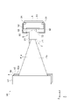
- FIG. 1 is a diagram showing a schematic configuration of an imaging system according to the first embodiment.
- FIG. 2 is a plan view of the image pickup unit shown in FIG.
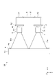
- FIG. 3 is a diagram showing a schematic configuration of an imaging unit according to a second embodiment.
- FIG. 4 is a plan view of the image pickup unit shown in FIG.
- FIG. 5 is a diagram showing the fields of view of the first lens and the second lens shown in FIG.
- FIG. 6 is a diagram showing a schematic configuration of an imaging unit according to a third embodiment.
- FIG. 7 is a plan view of the image pickup unit shown in FIG.
- FIG. 1 is a diagram showing a schematic configuration of an imaging system according to the first embodiment of the present disclosure.
- FIG. 2 is a plan view of the image pickup unit shown in FIG.
- the imaging system 1 of the first embodiment is a device for acquiring a radiographic image of an object A.
- the imaging system 1 is a scintillator double-sided observation type X-ray imaging system.
- the imaging system 1 is applied to, for example, in-line X-ray examination.
- the image pickup system 1 is excellent in the discrimination performance of a substance composed of, for example, a light element.
- the image pickup system 1 is applied to fields such as food inspection and battery inspection.
- the object A contains, for example, a substance composed of a light element. In the field of food inspection, for example, the presence or absence of foreign matter being caught is inspected. Examples of such substances include food waste, hair, vinyl, insects, bones in meat and the like.
- the image pickup system 1 emits radiation L such as white X-rays toward the transport device 20 that transports the object A in a predetermined transport direction D (X-axis direction) and the object A that is transported by the transport device 20. It includes a radiation source 30 and an image pickup unit 3A that executes image processing based on an image signal corresponding to the radiation L transmitted through the object A.
- the transport device 20 has, for example, a belt conveyor 21 that moves in an orbit.
- the object A is placed or held on the transport surface 21a of the belt conveyor 21.
- the belt conveyor 21 is a transfer stage or a transfer unit.
- the transport device 20 includes a drive source (not shown) that drives the belt conveyor 21.
- the transport device 20 is configured to transport the object A in the transport direction D at a constant speed. In other words, the object A is transported on the predetermined transport path P by the transport device 20.
- the transport direction D is the horizontal direction.
- the transport path P is linear.
- the direction in which the transport path P extends is parallel to the transport direction D.
- the transport timing and transport speed of the object A in the transport device 20 are preset and controlled by the control unit.
- the image pickup system 1 is compatible with all types of transport devices 20.
- the transport direction D and the transport path P may be horizontal.
- the transport direction D and the transport path P may be inclined with respect to the horizontal.
- the transport path P does not have to be linear and may be curved.
- the transport direction D may be a tangent line in a portion of the transport path P that overlaps the irradiation region of radiation.
- the transport device 20 does not have to have a physical transport surface 21a.
- the transport device 20 may transport the object A in a state of being lifted by air.
- the transport device 20 may transport the object A by discharging the object A into the air.
- the transport path P may be, for example, a parabolic shape.
- the transport device 20 may have a roller conveyor including a plurality of rollers.
- the radiation source 30 emits radiation L.
- the radiation L is, for example, a cone beam X-ray.
- the radiation source 30 may be a microfocus X-ray source or a millifocus X-ray source.
- the radiation L emitted from the radiation source 30 forms a radiation flux.
- the region where the radiation flux exists is the emission region of the radiation source 30.
- the image pickup unit 3A is arranged on the side opposite to the radiation source 30 with respect to the transport surface 21a of the belt conveyor 21.
- the image pickup unit 3A is attached to the transport device 20 so as not to interfere with the circulation of the belt conveyor 21.
- the image pickup unit 3A is arranged with some space from the transport unit so as not to interfere with the movement of the transport unit such as a belt conveyor or a roller conveyor.
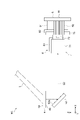
- the image pickup unit 3A includes a scintillator 4, a first mirror 51, a second mirror 52, a first sensor module 6, a second sensor module 7, a processing board (image processing unit, control unit) 8, and a first. It includes a connecting member 91 and a second connecting member 92.
- the scintillator 4 is a wavelength conversion member.
- the scintillator 4 emits scintillation light by incident radiation L transmitted through the object A.
- the scintillator 4 has a rectangular plate shape extending in the detection width direction (Y-axis direction).
- the scintillator 4 has a first surface 4a which is an incident surface of the radiation L, and a second surface 4b which faces the first surface 4a in the Z-axis direction.
- the first surface 4a and the second surface 4b are parallel to the transport surface 21a of the belt conveyor 21.
- the first surface 4a faces the radiation source 30 side.
- the scintillator 4 converts the radiation L transmitted through the object A into scintillation light (visible light).
- X-rays having relatively low energy are converted into scintillation light S1 by the first surface 4a of the scintillator 4, and are output from the first surface 4a. Further, X-rays having relatively high energy are converted into scintillation light S2 by the second surface 4b of the scintillator 4, and output from the second surface 4b.
- the scintillator 4 is, for example, Gd 2 O 2 S: Tb, Gd 2 O 2 S: Pr, CsI: Tl, CdWO 4 , CaWO 4 , Gd 2SiO 5 : Ce, Lu 0.4 Gd 1.6SiO 5 , Bi 4 Ge 3 O. 12 , Lu 2SiO 5 : Ce, Y 2SiO 5 , YAlO 3 : Ce, Y 2 O 2 S: Tb, YTaO 4 : Tm, YAG: Ce, YAG: Pr, YGAG : Ce, YGAG: Pr, GAGG: It consists of Ce etc.
- the thickness of the scintillator 4 is set to an appropriate value depending on the energy band of the radiation to be detected in the range of several ⁇ m to several mm.
- the scintillator 4 may be composed of one scintillator.
- the scintillator 4 may be a combination of a plurality of scintillators. When combining a plurality of scintillators, the types of scintillators may be the same or different.
- the first mirror 51 is, for example, a mirror made of aluminum-deposited glass or mirror-processed metal.
- the first mirror 51 is arranged on the radiation source 30 side with respect to the scintillator 4.
- the first mirror 51 has a rectangular plate shape extending in the detection width direction (Y-axis direction).
- the first mirror 51 has a reflecting surface 51a.
- the reflective surface 51a has an acute angle with respect to the first surface 4a of the scintillator 4.
- the reflective surface 51a faces diagonally with respect to the first surface 4a and also diagonally with respect to the first sensor module 6.
- the reflecting surface 51a reflects the scintillation light S1 emitted from the first surface 4a toward the first sensor module 6.
- the second mirror 52 is, for example, a mirror made of aluminum-deposited glass or mirror-processed metal.
- the second mirror 52 is arranged on the side opposite to the first mirror 51 with respect to the scintillator 4.
- the second mirror 52 has a rectangular plate shape extending in the detection width direction (Y-axis direction).
- the second mirror 52 has a reflecting surface 52a.
- the reflective surface 52a has an acute angle with respect to the second surface 4b of the scintillator 4.
- the reflective surface 52a faces obliquely with respect to the second surface 4b and also diagonally with respect to the second sensor module 7.
- the reflecting surface 52a reflects the scintillation light S2 emitted from the second surface 4b toward the second sensor module 7.
- the reflecting surface 51a has a sufficient area for reflecting the scintillation light S1 emitted in the normal direction of the first surface 4a.
- the reflecting surface 52a has a sufficient area for reflecting the scintillation light S2 emitted in the normal direction of the second surface 4b.
- the angle between the reflecting surface 51a and the first surface 4a and the angle between the reflecting surface 52a and the second surface 4b are each within a range of 40 degrees or more and 50 degrees or less. In this embodiment, these angles are 45 degrees. These angles may be determined based on the arrangement of the radiation source 30 and the position of the slit of the housing described later. The arrangement of the first sensor module 6 and the second sensor module 7 may be appropriately adjusted depending on the magnitude of these angles.
- the first sensor module 6 is separated from the scintillator 4 on one side (in-plane direction of the first surface 4a and the second surface 4b of the scintillator 4) in the X-axis direction (the wake side of the transport direction D from the scintillator 4). Is arranged.
- the first sensor module 6 is arranged on the first surface 4a side of the scintillator 4 in the Z-axis direction (the direction opposite to the first surface 4a and the second surface 4b of the scintillator 4).
- the first sensor module 6 detects the scintillation light S1 emitted from the first surface 4a due to the incident of the radiation L as the first scintillation light.
- the first scintillation light refers to the scintillation light detected by the first sensor module.
- the first sensor module 6 performs imaging according to the movement of the object A.
- the first sensor module 6 is a lens coupling type detector. Specifically, the first sensor module 6 has a first lens 61, a first body 62, and a first sensor 63.
- the first lens 61 is attached to the first body 62.
- the first lens 61 faces the reflection surface 51a of the first mirror 51 in the X-axis direction.
- the optical axis of the first lens 61 is parallel to the X-axis direction.
- the focus of the first lens 61 is aligned with the reflecting surface 51a.
- the field of view 61a of the first lens 61 covers a wide range of the reflecting surface 51a in the Y-axis direction.
- the first lens 61 collects the scintillation light S1 reflected by the reflecting surface 51a.
- the first sensor 63 is provided in the first body 62. The first sensor 63 detects the scintillation light S1 focused by the first lens 61, and outputs a first image signal corresponding to the detection result.
- the first sensor 63 is an image sensor.
- the first sensor 63 is, for example, a general line sensor, a multi-line sensor, or an area image sensor capable of TDI (time delay integration) drive.
- the first sensor 63 is, for example, a CCD area image sensor or a CMOS image sensor.
- the first sensor 63 has an element row in which a plurality of light receiving elements are arranged in a row in the pixel direction.
- the image pitches of the plurality of light receiving elements may be the same or different.
- a plurality of element trains are arranged in a plurality of stages in the integration direction corresponding to the moving direction of the object A.
- the first sensor 63 has a scan direction corresponding to the transport direction D of the object A and a line direction orthogonal to the scan direction.
- This scanning direction is the above-mentioned integration direction and is parallel to the Z-axis direction.
- the line direction is the pixel direction described above, and is parallel to the Y-axis direction.
- the scanning direction is the direction converted from the transport direction D via the first mirror 51. In this embodiment, the scanning direction is changed by 90 degrees from the transport direction D.
- the first sensor 63 is controlled by the control unit to transfer charges in accordance with the movement of the object A. That is, the first sensor 63 transfers charges on the light receiving surface in synchronization with the movement of the object A by the transport device 20. This makes it possible to obtain a radiographic image having a good S / N ratio.
- the control unit controls the radiation source 30 and the first sensor module 6 to turn on the radiation source 30 in accordance with the imaging timing of the first sensor module 6. There may be.
- the first sensor module 6 may be controlled by a signal from an encoder provided on the stage.
- the second sensor module 7 is arranged away from the scintillator 4 on one side in the X-axis direction.
- the second sensor module 7 is arranged on the second surface 4b side of the scintillator 4 in the Z-axis direction.
- the second sensor module 7 detects the scintillation light S2 emitted from the second surface 4b due to the incident of the radiation L as the second scintillation light.
- the second scintillation light refers to the scintillation light detected by the second sensor module.
- the second sensor module 7 performs imaging according to the movement of the object A.
- the second sensor module 7 is a lens coupling type detector. Specifically, the second sensor module 7 has a second lens 71, a second body 72, and a second sensor 73.
- the second lens 71 is attached to the second body 72.
- the second lens 71 faces the reflection surface 52a of the second mirror 52 in the X-axis direction.
- the optical axis of the second lens 71 is parallel to the X-axis direction.
- the focus of the second lens 71 is aligned with the reflecting surface 52a.
- the field of view 71a of the second lens 71 covers a wide range of the reflecting surface 52a in the Y-axis direction.
- the second lens 71 collects the scintillation light S2 reflected by the reflecting surface 52a.
- the second sensor 73 is provided in the second body 72.
- the second sensor 73 detects the scintillation light S2 focused by the second lens 71, and outputs a second image signal corresponding to the detection result.
- the second sensor 73 has the same configuration as the first sensor 63, and is controlled in the same manner as the first sensor 63. A detailed description of the second sensor 73 will be omitted.
- the processing board 8 has a board 81 and a processor (not shown) attached to the board 81.
- the processing board 8 functions as an image processing unit that executes image processing based on the first image signal output from the first sensor 63 and the second image signal output from the second sensor 73.
- the processing substrate 8 has magnification correction, luminance value correction, dark correction, shooting correction, affine transformation processing, edge enhancement processing, and noise for at least one of the first image signal and the second image signal. Performs image processing such as removal processing, bilateral filter processing, or angle of view adjustment.
- the processing board 8 outputs a radiographic image created by executing image processing to a computer.
- the processing board 8 functions as a control unit that controls the image pickup condition by the first sensor 63 and the image pickup condition by the second sensor 73. Specifically, the processing board 8 sets the exposure time, gain, imaging frequency, imaging timing, and the like for the first sensor 63 and the second sensor 73. Further, the processing board 8 adjusts the image pickup timing of the first sensor 63, the image pickup timing of the second sensor 73, and the image processing timing as an image processing unit or a control unit. This facilitates processing such as matching the detection ranges of the first image signal and the second image signal, and comparing or synthesizing the first image signal and the second image signal. The processing board 8 may control at least one of the first image signal and the second image signal to delay the output within a range exceeding the exposure time.
- one processing board 8 is provided for the first sensor module 6 and the second sensor module 7. That is, the processing board 8 is shared with the first sensor module 6 and the second sensor module 7.
- the first connection member 91 electrically connects the first sensor module 6 and the processing board 8. Specifically, the first connection member 91 electrically connects the first sensor 63 and the image processing processor via the wiring provided on the first body 62 and the wiring provided on the substrate 81. There is.
- the second connection member 92 electrically connects the second sensor module 7 and the processing board 8. Specifically, the second connecting member 92 electrically connects the second sensor 73 and the image processing processor via the wiring provided on the second body 72 and the wiring provided on the substrate 81. There is. As a result, the first image signal and the second image signal can be output to the processing board 8.
- Each of the first connecting member 91 and the second connecting member 92 has flexibility. Each of the first connecting member 91 and the second connecting member 92 can be easily deformed by receiving a load corresponding to, for example, the force of a worker's finger.
- Each of the first connecting member 91 and the second connecting member 92 is composed of, for example, a cable, a connector, or the like.
- Each of the first connecting member 91 and the second connecting member 92 is composed of, for example, a harness, a connector, or the like.
- Each of the first connecting member 91 and the second connecting member 92 is, for example, a flexible connector.
- the image pickup unit 3A has, for example, a rectangular parallelepiped housing (not shown).
- the scintillator 4, the first mirror 51, the second mirror 52, the first sensor module 6, the second sensor module 7, and the processing board 8 are housed in a housing.
- the scintillator 4, the first mirror 51, the second mirror 52, the first sensor module 6, the second sensor module 7, and the processing board 8 are each held by a housing.
- a slit is formed in the wall portion on the side of the radiation source 30 in the housing to allow the radiation L emitted from the radiation source 30 to pass through.
- the slit has a rectangular shape extending in the detection width direction (Y-axis direction), for example.
- the housing is made of, for example, a material that can shield X-rays.
- the housing is a so-called dark box.
- the housing may be made of metal, for example.
- the housing is made of, for example, aluminum, iron, stainless steel, or the like.
- the housing may include a protective material.
- the protective material is, for example, metal. Examples of the protective material include lead, tungsten, copper, iron, stainless steel and the like.
- the housing has a shape elongated in the transport direction D. The housing may be attached to the transport device 20.
- the imaging system 1 includes a control unit (not shown).
- the control unit controls the radiation source 30 based on the values of the tube voltage and tube current of the radiation source 30 stored by the user's input or the like.
- the control unit controls each of the first sensor module 6 and the second sensor module 7 based on the exposure times of the first sensor module 6 and the second sensor module 7 stored by the user's input or the like.
- the control unit and the image processing processor of the processing board 8 may be separate processors or the same processor.
- the distance between the reflection surface 51a in the Z-axis direction and the first surface 4a of the scintillator 4 is smaller than the distance between the reflection surface 52a in the Z-axis direction and the second surface 4b of the scintillator 4. That is, the optical path length of the scintillation light S1 between the reflecting surface 51a and the first surface 4a in the Z-axis direction is larger than the optical path length of the scintillation light S2 between the reflecting surface 52a and the second surface 4b in the Z-axis direction. It's getting smaller.
- the distance between the first lens 61 and the first surface 4a of the scintillator 4 in the Z-axis direction is smaller than the distance between the second lens 71 and the second surface 4b of the scintillator 4 in the Z-axis direction.
- the distance between the optical axis of the first lens 61 and the first surface 4a is smaller than the distance between the optical axis of the second lens 71 and the second surface 4b.
- the position of the second lens 71 in the X-axis direction is closer to the scintillator 4 side than the position of the first lens 61 in the X-axis direction.
- the optical path length of the scintillation light S2 between the reflection surface 52a and the second lens 71 in the X-axis direction is larger than the optical path length of the scintillation light S1 between the reflection surface 51a and the first lens 61 in the X-axis direction. It's getting smaller.
- the optical path length of the scintillation light S1 between the first surface 4a of the scintillator 4 and the first lens 61 becomes equal to the optical path length of the scintillation light S2 between the second surface 4b of the scintillator 4 and the second lens 71.
- the first mirror 51 and the first sensor module 6 are brought close to the scintillator 4 in the Z-axis direction, and the optical path length of the scintillation light S1 and the optical path length of the scintillation light S2 are matched. There is. As a result, the scintillator 4 can be brought close to the object A, and a radiographic image of the object A can be acquired with high accuracy.
- each of the first connecting member 91 and the second connecting member 92 has flexibility. That is, while the first sensor module 6 and the second sensor module 7 are connected to the processing board 8 by the first connecting member 91 and the second connecting member 92, the positions with respect to the processing board 8 can be adjusted. There is. Thereby, by adjusting the positions of the first sensor module 6 and the second sensor module 7, the positional relationship as described above can be easily adjusted.
- the object A is transported in the transport direction D by the transport device 20. Further, the radiation source 30 emits the radiation L toward the object A. The radiation L transmitted through the object A is incident on the first surface 4a. Next, the radiation L is converted into scintillation light by the scintillator 4. The scintillation light S1 emitted from the first surface 4a is reflected by the first mirror 51 and is imaged on the first sensor 63 by the first lens 61 of the first sensor module 6. The first sensor 63 captures the scintillation light S1 (scintillation image) imaged by the first lens 61.
- the first sensor module 6 outputs the radiographic image data (first image signal) obtained by imaging to the processing board 8. Similar to the first sensor module 6, the second sensor module 7 captures the scintillation light S2 and outputs the obtained radiographic image data (second image signal) to the processing substrate 8.
- the processing substrate 8 inputs radiographic image data, executes predetermined processing such as image processing on the input radiographic image data, and creates a radiographic image.
- the processing board 8 outputs the created radiographic image to a computer.
- the computer displays the radiographic image output from the processing board 8. As a result, a radiographic image obtained by observing both sides of the object A can be obtained.
- the processing substrate 8 for processing the first image signal and the second image signal from the first sensor module 6 and the second sensor module 7 is shared. Therefore, the configuration can be simplified as compared with the configuration in which the processing board is provided for each sensor module. Further, in the image pickup unit 3A, in order to standardize the processing board 8, each of the first connecting member 91 and the second connecting member 92 connecting the first sensor module 6 and the second sensor module 7 to the processing board 8 is flexible. have. Therefore, the imaging positions of the first sensor module 6 and the second sensor module 7 can be adjusted separately, and a sufficient degree of freedom in adjusting the imaging position can be ensured.
- the image pickup unit 3A includes a scintillator 4 that emits scintillation lights S1 and S2 when radiation L is incident. This makes it possible to improve workability when incorporating the image pickup unit 3A into the image pickup system 1.
- the scintillator 4 has a first surface 4a which is an incident surface of the radiation L and a second surface 4b which faces the first surface 4a.
- the first sensor module 6 is arranged on the first surface 4a side of the scintillator 4 in the Z-axis direction.
- the first sensor module 6 detects the scintillation light S1 emitted from the first surface 4a due to the incident of the radiation L as the first scintillation light.
- the second sensor module 7 is arranged on the second surface 4b side of the scintillator 4 in the Z-axis direction.
- the second sensor module 7 detects the scintillation light S2 emitted from the second surface 4b due to the incident of the radiation L as the second scintillation light.
- the first sensor module 6 and the second sensor module 7 are arranged apart from the scintillator 4 on one side in the X-axis direction.
- the distance between the first lens 61 of the first sensor module 6 and the first surface 4a in the Z-axis direction is smaller than the distance between the second lens 71 and the second surface 4b of the second sensor module 7 in the Z-axis direction. ing.
- the position of the second lens 71 in the X-axis direction is closer to the scintillator 4 side than the position of the first lens 61 in the Z-axis direction.
- the optical path length of the scintillation light S1 (first scintillation light) and the optical path length of the scintillation light S2 (second scintillation light) are matched. Can be done.
- the configuration can be simplified and the degree of freedom in adjusting the image pickup position can be sufficiently secured.
- FIG. 3 is a diagram showing a schematic configuration of an imaging unit according to the second embodiment of the present disclosure.
- FIG. 4 is a plan view of the image pickup unit shown in FIG.
- the first sensor module 6 and the second sensor module 7 are arranged on the first surface 4a side of the scintillator 4 and in the Y-axis direction. It differs from the image pickup unit 3A of the first embodiment in that it is lined up and does not include the second mirror 52.
- the imaging system according to the second embodiment is a scintillator surface observation type X-ray imaging system.
- the first sensor module 6 and the second sensor module 7 are arranged on the first surface 4a side of the scintillator 4 in the Z-axis direction and are arranged in the Y-axis direction (in-plane direction of the first surface 4a). I'm out.
- the first sensor module 6 detects the scintillation light S1 emitted from the first surface 4a due to the incident of the radiation L as the first scintillation light.
- the second sensor module 7 detects the scintillation light S1 emitted from the first surface 4a due to the incident of the radiation L as the second scintillation light.
- the distance between the first lens 61 of the first sensor module 6 and the scintillator 4 in the Z-axis direction is equal to the distance between the second lens 71 of the second sensor module 7 and the scintillator 4 in the Z-axis direction.
- the distance between the optical axis of the first lens 61 and the first surface 4a is equal to the distance between the optical axis of the second lens 71 and the first surface 4a. That is, the optical path length of the scintillation light S1 (the scintlation light S1 incident on the first lens 61) between the reflection surface 51a and the first surface 4a of the first mirror 51 in the Z-axis direction is the reflection surface 51a and the first surface. It is equal to the optical path length in the Z-axis direction of the scintillation light S1 (the scintillation light S1 incident on the second lens 71) with and from 4a.
- the positions of the first lens 61 and the second lens 71 in the X-axis direction with respect to the scintillator 4 are the same. That is, the optical path length of the scintillation light S1 between the reflection surface 51a and the first lens 61 in the X-axis direction is equal to the optical path length of the scintillation light S1 between the reflection surface 51a and the second lens 71 in the X-axis direction. It has become. As described above, the optical path length of the scintillation light S1 between the first surface 4a of the scintillator 4 and the first lens 61 is the optical path length of the scintillation light S1 between the first surface 4a of the scintillator 4 and the second lens 71. Is equal to.
- FIG. 5 is a diagram showing the fields of view of the first lens 61 and the second lens 71 shown in FIG. In FIG. 5, the illustration of the first mirror 51 is omitted. As shown in FIG. 5, a part of the visual field of the first lens 61 and the second lens 71 overlap each other in the Y-axis direction. Specifically, when viewed from the Z-axis direction, the range in the Y-axis direction of the field of view 61a of the first lens 61 with respect to the first surface 4a and the range of the field of view 61a of the second lens 71 with respect to the first surface 4a in the Y-axis direction. Some of them overlap with each other.
- the width of the overlapping region R in the Y-axis direction can be adjusted by adjusting the positions of the first sensor module 6 and the second sensor module 7 in the Y-axis direction.
- the image pickup unit 3B by arranging the first sensor module 6 and the second sensor module 7 in the Y-axis direction, the field of view as the image pickup unit 3B in the Y-axis direction is widened, and the overlapping region R is appropriately set.
- the visual field 61a and the visual field 71a in the Y-axis direction are continuous.
- the positions of the first sensor module 6 and the second sensor module 7 with respect to the processing board 8 are respectively. Is adjustable. Thereby, by adjusting the positions of the first sensor module 6 and the second sensor module 7, the positional relationship as described above can be easily adjusted.
- the scintillator 4 has a first surface 4a which is an incident surface of the radiation L and a second surface 4b which faces the first surface 4a.
- the first sensor module 6 and the second sensor module 7 are arranged on the first surface 4a side of the scintillator 4 in the Z-axis direction and are arranged in the Y-axis direction.
- the first sensor module 6 detects the scintillation light S1 emitted from the first surface 4a due to the incident of the radiation L as the first scintillation light.
- the second sensor module 7 detects the scintillation light S1 emitted from the first surface 4a due to the incident of the radiation L as the second scintillation light.
- the scintillation light S1 from one side of the scintillator 4 can be accurately detected by the first sensor module 6 and the second sensor module 7, respectively.
- the first sensor module 6 and the second sensor module 7 are arranged apart from the scintillator 4 on one side in the X-axis direction.
- the distance between the first lens 61 of the first sensor module 6 and the scintillator 4 in the Z-axis direction is equal to the distance between the second lens 71 of the second sensor module 7 and the scintillator 4 in the Z-axis direction.
- the positions of the first lens 61 and the second lens 71 with respect to the scintillator 4 are the same in the X-axis direction. Thereby, the first lens 61 and the second lens 71 can be shared.
- the image correction caused by the difference between the optical path length of the scintillation light S1 (first scintillation light) incident on the first lens 61 and the optical path length of the scintillation light S1 (second scintillation light) incident on the second lens 71 is performed. Since it is unnecessary, it is possible to avoid complication of image processing on the processing substrate 8.
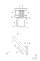
- FIG. 6 is a diagram showing a schematic configuration of an imaging unit according to a third embodiment of the present disclosure.
- FIG. 7 is a plan view of the image pickup unit shown in FIG.
- the first sensor module 6 and the second sensor module 7 are arranged on the second surface 4b side of the scintillator 4, and a second. It is different from the image pickup unit 3B of the second embodiment in that the first mirror 51 is not provided and the second mirror 52 is provided.
- the imaging system according to the third embodiment is a scintillator backside observation type X-ray imaging system.
- the first sensor module 6 and the second sensor module 7 are arranged on the second surface 4b side of the scintillator 4 in the Z-axis direction.
- the first sensor module 6 detects the scintillation light S2 emitted from the second surface 4b due to the incident of the radiation L as the first scintillation light.
- the second sensor module 7 detects the scintillation light S2 emitted from the second surface 4b due to the incident of the radiation L as the second scintillation light.
- the distance between the optical axis of the first lens 61 and the second surface 4b is the distance between the optical axis of the second lens 71 and the second surface 4b.
- the positions of the first lens 61 and the second lens 71 in the X-axis direction with respect to the scintillator 4 are the same.
- a part of the visual field of the first lens 61 and the second lens 71 overlap each other in the Y-axis direction.
- the scintillator 4 has a first surface 4a which is an incident surface of the radiation L and a second surface 4b which faces the first surface 4a.
- the first sensor module 6 and the second sensor module 7 are arranged on the second surface 4b side of the scintillator 4 in the Z-axis direction and are arranged in the Y-axis direction.
- the first sensor module 6 detects the scintillation light S2 emitted from the second surface 4b due to the incident of the radiation L as the first scintillation light.
- the second sensor module 7 detects the scintillation light S2 emitted from the second surface 4b due to the incident of the radiation L as the second scintillation light.
- the scintillation light S2 from one side of the scintillator 4 can be accurately detected by the first sensor module 6 and the second sensor module 7, respectively.
- the present disclosure is not limited to the above embodiment.
- the image pickup units 3A, 3B, 3C are provided with the scintillator 4, but the image pickup units 3A, 3B, 3C may not be provided with the scintillator 4.
- the scintillator 4 does not have to be configured as the image pickup unit 3A, 3B, 3C.
- the scintillator 4 may be configured as an imaging system.
- Imaging system 3A, 3B, 3C ... Imaging unit, 4 ... Scintillator, 4a ... 1st surface, 4b ... 2nd surface, 6 ... 1st sensor module, 7 ... 2nd sensor module, 8 ... Processing board, 20 ... transport device, 30 ... radiation source, 61 ... first lens, 61a, 71a ... field of view, 63 ... first sensor, 71 ... second lens, 73 ... second sensor, 91 ... first connecting member, 92 ... second Connecting member, A ... object, L ... radiation, S1, S2 ... scintillation light.
Abstract
Description
図1は、本開示の第1実施形態に係る撮像システムの概略構成を示す図である。図2は、図1に示される撮像ユニットの平面図である。図1及び図2に示すように、第1実施形態の撮像システム1は、対象物Aの放射線画像を取得するための装置である。撮像システム1は、シンチレータ両面観察方式のX線撮影システムである。撮像システム1は、たとえばインラインX線検査に適用される。撮像システム1は、たとえば軽元素からなる物質の弁別性能に優れている。撮像システム1は、たとえば、食品検査やバッテリー検査などの分野に適用される。対象物Aは、たとえば、軽元素からなる物質を含有する。食品検査の分野では、たとえば異物の噛み込みの有無が検査される。このような物質としては、たとえば、食品のくず、髪の毛、ビニール、虫、肉の中の骨等が挙げられる。 [First Embodiment]
FIG. 1 is a diagram showing a schematic configuration of an imaging system according to the first embodiment of the present disclosure. FIG. 2 is a plan view of the image pickup unit shown in FIG. As shown in FIGS. 1 and 2, the imaging system 1 of the first embodiment is a device for acquiring a radiographic image of an object A. The imaging system 1 is a scintillator double-sided observation type X-ray imaging system. The imaging system 1 is applied to, for example, in-line X-ray examination. The image pickup system 1 is excellent in the discrimination performance of a substance composed of, for example, a light element. The image pickup system 1 is applied to fields such as food inspection and battery inspection. The object A contains, for example, a substance composed of a light element. In the field of food inspection, for example, the presence or absence of foreign matter being caught is inspected. Examples of such substances include food waste, hair, vinyl, insects, bones in meat and the like.
図3は、本開示の第2実施形態に係る撮像ユニットの概略構成を示す図である。図4は、図3に示される撮像ユニットの平面図である。図3及び図4に示すように、第2実施形態に係る撮像ユニット3Bは、第1センサモジュール6及び第2センサモジュール7がシンチレータ4の第1面4a側に配置されると共にY軸方向に並んでいる点、及び第2ミラー52を備えていない点で第1実施形態の撮像ユニット3Aと異なっている。 [Second Embodiment]
FIG. 3 is a diagram showing a schematic configuration of an imaging unit according to the second embodiment of the present disclosure. FIG. 4 is a plan view of the image pickup unit shown in FIG. As shown in FIGS. 3 and 4, in the
図6は、本開示の第3実施形態に係る撮像ユニットの概略構成を示す図である。図7は、図6に示される撮像ユニットの平面図である。図6及び図7に示すように、第3実施形態に係る撮像ユニット3Cは、第1センサモジュール6及び第2センサモジュール7がシンチレータ4の第2面4b側に配置されている点、及び第1ミラー51を備えず第2ミラー52を備えている点で第2実施形態の撮像ユニット3Bと異なっている。 [Third Embodiment]
FIG. 6 is a diagram showing a schematic configuration of an imaging unit according to a third embodiment of the present disclosure. FIG. 7 is a plan view of the image pickup unit shown in FIG. As shown in FIGS. 6 and 7, in the
本開示は、上記実施形態に限られるものではない。たとえば、撮像ユニット3A,3B,3Cがシンチレータ4を備えていたが、撮像ユニット3A,3B,3Cは、シンチレータ4を備えていなくてもよい。シンチレータ4は、撮像ユニット3A,3B,3Cの構成ではなくてもよい。シンチレータ4は、撮像システムの構成であってもよい。 [Modification example]
The present disclosure is not limited to the above embodiment. For example, the
Claims (9)
- 第1シンチレーション光を集光する第1レンズ、及び前記第1レンズにより集光された前記第1シンチレーション光を検出し、検出結果に対応する第1画像信号を出力する第1センサを有する第1センサモジュールと、
第2シンチレーション光を集光する第2レンズ、及び前記第2レンズにより集光された前記第2シンチレーション光を検出し、検出結果に対応する第2画像信号を出力する第2センサを有する第2センサモジュールと、
前記第1画像信号及び前記第2画像信号に基づく画像処理を実行する処理基板と、
前記第1センサモジュールと前記処理基板とを電気的に接続する可撓性の第1接続部材と、
前記第2センサモジュールと前記処理基板とを電気的に接続する可撓性の第2接続部材と、を備える、撮像ユニット。 A first lens having a first lens that collects the first scintillation light and a first sensor that detects the first scintillation light collected by the first lens and outputs a first image signal corresponding to the detection result. With the sensor module
A second lens having a second lens that collects the second scintillation light and a second sensor that detects the second scintillation light focused by the second lens and outputs a second image signal corresponding to the detection result. With the sensor module
A processing board that executes image processing based on the first image signal and the second image signal, and
A flexible first connection member that electrically connects the first sensor module and the processing board, and
An image pickup unit comprising a flexible second connection member that electrically connects the second sensor module and the processing board. - 放射線の入射によってシンチレーション光を出射するシンチレータを更に備える、請求項1に記載の撮像ユニット。 The imaging unit according to claim 1, further comprising a scintillator that emits scintillation light when radiation is incident.
- 前記シンチレータは、前記放射線の入射面となる第1面と、前記第1面と対向する第2面と、を有し、
前記第1センサモジュールは、前記第1面と前記第2面との対向方向において前記シンチレータの前記第1面側に配置され、前記放射線の入射によって前記第1面から出射する前記シンチレーション光を前記第1シンチレーション光として検出し、
前記第2センサモジュールは、前記対向方向において前記シンチレータの前記第2面側に配置され、前記放射線の入射によって前記第2面から出射する前記シンチレーション光を前記第2シンチレーション光として検出する、請求項2に記載の撮像ユニット。 The scintillator has a first surface that is an incident surface of the radiation and a second surface that faces the first surface.
The first sensor module is arranged on the first surface side of the scintillator in a direction facing the first surface and the second surface, and the scintillation light emitted from the first surface due to the incident of the radiation is emitted from the first surface. Detected as the first scintillation light,
The second sensor module is arranged on the second surface side of the scintillator in the facing direction, and detects the scintillation light emitted from the second surface by the incident of the radiation as the second scintillation light. 2. The imaging unit according to 2. - 前記第1センサモジュール及び前記第2センサモジュールは、前記第1面及び前記第2面の面内方向の一側において前記シンチレータから離間して配置されており、
前記対向方向における前記第1センサモジュールの前記第1レンズと前記第1面との間隔は、前記対向方向における前記第2センサモジュールの前記第2レンズと前記第2面との間隔よりも小さくなっており、
前記第2レンズの前記面内方向の位置は、前記第1レンズの前記面内方向の位置よりも前記シンチレータ側に近接している、請求項3に記載の撮像ユニット。 The first sensor module and the second sensor module are arranged apart from the scintillator on one side of the first surface and the second surface in the in-plane direction.
The distance between the first lens of the first sensor module and the first surface in the facing direction is smaller than the distance between the second lens and the second surface of the second sensor module in the facing direction. And
The imaging unit according to claim 3, wherein the position of the second lens in the in-plane direction is closer to the scintillator side than the position of the first lens in the in-plane direction. - 前記シンチレータは、前記放射線の入射面となる第1面と、前記1面と対向する第2面と、を有し、
前記第1センサモジュール及び前記第2センサモジュールは、前記第1面と前記第2面との対向方向において前記シンチレータの前記第1面側に配置されると共に前記第1面の面内方向に並んでおり、
前記第1センサモジュールは、前記放射線の入射によって前記第1面から出射する前記シンチレーション光を前記第1シンチレーション光として検出し、
前記第2センサモジュールは、前記放射線の入射によって前記第1面から出射する前記シンチレーション光を前記第2シンチレーション光として検出する、請求項2に記載の撮像ユニット。 The scintillator has a first surface that is an incident surface of the radiation and a second surface that faces the first surface.
The first sensor module and the second sensor module are arranged on the first surface side of the scintillator in the direction opposite to the first surface and the second surface, and are arranged in the in-plane direction of the first surface. And
The first sensor module detects the scintillation light emitted from the first surface due to the incident of the radiation as the first scintillation light.
The imaging unit according to claim 2, wherein the second sensor module detects the scintillation light emitted from the first surface due to the incident of the radiation as the second scintillation light. - 前記シンチレータは、前記放射線の入射面となる第1面と、前記第1面と対向する第2面と、を有し、
前記第1センサモジュール及び前記第2センサモジュールは、前記第1面と前記第2面との対向方向において前記シンチレータの前記第2面側に配置されると共に前記第2面の面内方向に並んでおり、
前記第1センサモジュールは、前記放射線の入射によって前記第2面から出射する前記シンチレーション光を前記第1シンチレーション光として検出し、
前記第2センサモジュールは、前記放射線の入射によって前記第2面から出射する前記シンチレーション光を前記第2シンチレーション光として検出する、請求項2に記載の撮像ユニット。 The scintillator has a first surface that is an incident surface of the radiation and a second surface that faces the first surface.
The first sensor module and the second sensor module are arranged on the second surface side of the scintillator in the direction opposite to the first surface and the second surface, and are arranged in the in-plane direction of the second surface. And
The first sensor module detects the scintillation light emitted from the second surface due to the incident of the radiation as the first scintillation light.
The imaging unit according to claim 2, wherein the second sensor module detects the scintillation light emitted from the second surface due to the incident of the radiation as the second scintillation light. - 前記第1面及び前記第2面の前記面内方向において、前記第1センサモジュールの前記第1レンズと前記第2センサモジュールの前記第2レンズとの視野一部同士が重なっている、請求項5又は6に記載の撮像ユニット。 A claim that a part of the field of view of the first lens of the first sensor module and the second lens of the second sensor module overlap each other in the in-plane direction of the first surface and the second surface. 5. The imaging unit according to 5.
- 前記第1センサモジュール及び前記第2センサモジュールは、前記第1面及び前記第2面の面内方向の一側において前記シンチレータから離間して配置されており、
前記対向方向における前記第1センサモジュールの前記第1レンズと前記シンチレータとの間隔は、前記対向方向における前記第2センサモジュールの前記第2レンズと前記シンチレータとの間隔と等しくなっており、
前記シンチレータに対する前記第1レンズ及び前記第2レンズの前記面内方向の位置が一致している、請求項5~7のいずれか一項に記載の撮像ユニット。 The first sensor module and the second sensor module are arranged apart from the scintillator on one side of the first surface and the second surface in the in-plane direction.
The distance between the first lens of the first sensor module and the scintillator in the facing direction is equal to the distance between the second lens of the second sensor module and the scintillator in the facing direction.
The imaging unit according to any one of claims 5 to 7, wherein the positions of the first lens and the second lens in the in-plane direction with respect to the scintillator are the same. - 対象物を搬送する搬送装置と、
前記搬送装置によって搬送される前記対象物に向けて放射線を出射する放射線源と、
前記対象物を透過した前記放射線に対応する画像信号に基づく画像処理を実行する請求項1~8のいずれか一項に記載の撮像ユニットと、を備える、撮像システム。 A transport device that transports objects and
A radiation source that emits radiation toward the object transported by the transport device,
An imaging system comprising the imaging unit according to any one of claims 1 to 8, which performs image processing based on an image signal corresponding to the radiation transmitted through the object.
Priority Applications (5)
| Application Number | Priority Date | Filing Date | Title |
|---|---|---|---|
| KR1020237015006A KR20230109134A (en) | 2020-11-25 | 2021-09-24 | Imaging unit and imaging system |
| JP2022565089A JPWO2022113507A1 (en) | 2020-11-25 | 2021-09-24 | |
| CN202180078988.1A CN116472474A (en) | 2020-11-25 | 2021-09-24 | Image pickup unit and image pickup system |
| EP21897485.5A EP4206745A1 (en) | 2020-11-25 | 2021-09-24 | Imaging unit and imaging system |
| US18/032,407 US20230400421A1 (en) | 2020-11-25 | 2021-09-24 | Imaging unit and imaging system |
Applications Claiming Priority (2)
| Application Number | Priority Date | Filing Date | Title |
|---|---|---|---|
| JP2020-195049 | 2020-11-25 | ||
| JP2020195049 | 2020-11-25 |
Publications (1)
| Publication Number | Publication Date |
|---|---|
| WO2022113507A1 true WO2022113507A1 (en) | 2022-06-02 |
Family
ID=81755522
Family Applications (1)
| Application Number | Title | Priority Date | Filing Date |
|---|---|---|---|
| PCT/JP2021/035165 WO2022113507A1 (en) | 2020-11-25 | 2021-09-24 | Imaging unit and imaging system |
Country Status (7)
| Country | Link |
|---|---|
| US (1) | US20230400421A1 (en) |
| EP (1) | EP4206745A1 (en) |
| JP (1) | JPWO2022113507A1 (en) |
| KR (1) | KR20230109134A (en) |
| CN (1) | CN116472474A (en) |
| TW (1) | TW202223372A (en) |
| WO (1) | WO2022113507A1 (en) |
Citations (4)
| Publication number | Priority date | Publication date | Assignee | Title |
|---|---|---|---|---|
| JP2002034961A (en) * | 2000-07-31 | 2002-02-05 | Konica Corp | Radiographing apparatus and radiographing method |
| JP2012154733A (en) | 2011-01-25 | 2012-08-16 | Hamamatsu Photonics Kk | Device for taking radiation image |
| JP2014179356A (en) * | 2011-07-21 | 2014-09-25 | Fujifilm Corp | Radiation image detector and radiograph device |
| JP2020139816A (en) * | 2019-02-27 | 2020-09-03 | 浜松ホトニクス株式会社 | Imaging unit and radiation image acquisition system |
-
2021
- 2021-09-24 JP JP2022565089A patent/JPWO2022113507A1/ja active Pending
- 2021-09-24 CN CN202180078988.1A patent/CN116472474A/en active Pending
- 2021-09-24 EP EP21897485.5A patent/EP4206745A1/en active Pending
- 2021-09-24 KR KR1020237015006A patent/KR20230109134A/en active Search and Examination
- 2021-09-24 WO PCT/JP2021/035165 patent/WO2022113507A1/en active Application Filing
- 2021-09-24 US US18/032,407 patent/US20230400421A1/en active Pending
- 2021-10-13 TW TW110137902A patent/TW202223372A/en unknown
Patent Citations (4)
| Publication number | Priority date | Publication date | Assignee | Title |
|---|---|---|---|---|
| JP2002034961A (en) * | 2000-07-31 | 2002-02-05 | Konica Corp | Radiographing apparatus and radiographing method |
| JP2012154733A (en) | 2011-01-25 | 2012-08-16 | Hamamatsu Photonics Kk | Device for taking radiation image |
| JP2014179356A (en) * | 2011-07-21 | 2014-09-25 | Fujifilm Corp | Radiation image detector and radiograph device |
| JP2020139816A (en) * | 2019-02-27 | 2020-09-03 | 浜松ホトニクス株式会社 | Imaging unit and radiation image acquisition system |
Also Published As
| Publication number | Publication date |
|---|---|
| KR20230109134A (en) | 2023-07-19 |
| EP4206745A1 (en) | 2023-07-05 |
| US20230400421A1 (en) | 2023-12-14 |
| CN116472474A (en) | 2023-07-21 |
| TW202223372A (en) | 2022-06-16 |
| JPWO2022113507A1 (en) | 2022-06-02 |
Similar Documents
| Publication | Publication Date | Title |
|---|---|---|
| US10746884B2 (en) | Radiation image acquisition device | |
| US10234406B2 (en) | Radiation image acquisition system | |
| JP5784916B2 (en) | Radiation image acquisition device | |
| CN106128540B (en) | Scintillator panel | |
| US20230344958A1 (en) | Imaging unit and radiation image acquisition system | |
| JP7457187B2 (en) | Imaging unit | |
| WO2022113507A1 (en) | Imaging unit and imaging system | |
| JP6671413B2 (en) | Radiation image acquisition device | |
| JP3204649U (en) | Radiation image acquisition device and imaging unit | |
| JP5973040B2 (en) | Radiation image acquisition device | |
| US11693132B2 (en) | Scintillator attachment structure in radiation imaging unit | |
| JP5706387B2 (en) | Scintillator plate and image acquisition device | |
| JP6345720B2 (en) | Radiation image acquisition device and method for adjusting radiation image acquisition device |
Legal Events
| Date | Code | Title | Description |
|---|---|---|---|
| 121 | Ep: the epo has been informed by wipo that ep was designated in this application |
Ref document number: 21897485 Country of ref document: EP Kind code of ref document: A1 |
|
| ENP | Entry into the national phase |
Ref document number: 2022565089 Country of ref document: JP Kind code of ref document: A |
|
| ENP | Entry into the national phase |
Ref document number: 2021897485 Country of ref document: EP Effective date: 20230327 |
|
| WWE | Wipo information: entry into national phase |
Ref document number: 202180078988.1 Country of ref document: CN |
|
| NENP | Non-entry into the national phase |
Ref country code: DE |