EP4206745A1 - Imaging unit and imaging system - Google Patents
Imaging unit and imaging system Download PDFInfo
- Publication number
- EP4206745A1 EP4206745A1 EP21897485.5A EP21897485A EP4206745A1 EP 4206745 A1 EP4206745 A1 EP 4206745A1 EP 21897485 A EP21897485 A EP 21897485A EP 4206745 A1 EP4206745 A1 EP 4206745A1
- Authority
- EP
- European Patent Office
- Prior art keywords
- sensor module
- lens
- scintillator
- scintillation light
- radiation
- Prior art date
- Legal status (The legal status is an assumption and is not a legal conclusion. Google has not performed a legal analysis and makes no representation as to the accuracy of the status listed.)
- Pending
Links
- 238000003384 imaging method Methods 0.000 title claims abstract description 119
- 238000012545 processing Methods 0.000 claims abstract description 71
- 239000000758 substrate Substances 0.000 claims abstract description 52
- 230000005855 radiation Effects 0.000 claims description 90
- 230000000007 visual effect Effects 0.000 claims description 26
- 238000001514 detection method Methods 0.000 claims description 11
- 230000003287 optical effect Effects 0.000 description 33
- 238000000034 method Methods 0.000 description 8
- XEEYBQQBJWHFJM-UHFFFAOYSA-N Iron Chemical compound [Fe] XEEYBQQBJWHFJM-UHFFFAOYSA-N 0.000 description 4
- 238000007689 inspection Methods 0.000 description 4
- 239000000463 material Substances 0.000 description 4
- 229910052751 metal Inorganic materials 0.000 description 4
- 239000002184 metal Substances 0.000 description 4
- 230000008569 process Effects 0.000 description 4
- 229910052782 aluminium Inorganic materials 0.000 description 3
- XAGFODPZIPBFFR-UHFFFAOYSA-N aluminium Chemical compound [Al] XAGFODPZIPBFFR-UHFFFAOYSA-N 0.000 description 3
- 238000012937 correction Methods 0.000 description 3
- 235000013305 food Nutrition 0.000 description 3
- 230000010354 integration Effects 0.000 description 3
- 230000001681 protective effect Effects 0.000 description 3
- 238000012546 transfer Methods 0.000 description 3
- 230000001154 acute effect Effects 0.000 description 2
- 230000004907 flux Effects 0.000 description 2
- 239000011521 glass Substances 0.000 description 2
- 238000003702 image correction Methods 0.000 description 2
- 229910052742 iron Inorganic materials 0.000 description 2
- 229910001220 stainless steel Inorganic materials 0.000 description 2
- 239000010935 stainless steel Substances 0.000 description 2
- 239000000126 substance Substances 0.000 description 2
- PXFBZOLANLWPMH-UHFFFAOYSA-N 16-Epiaffinine Natural products C1C(C2=CC=CC=C2N2)=C2C(=O)CC2C(=CC)CN(C)C1C2CO PXFBZOLANLWPMH-UHFFFAOYSA-N 0.000 description 1
- 229910004829 CaWO4 Inorganic materials 0.000 description 1
- RYGMFSIKBFXOCR-UHFFFAOYSA-N Copper Chemical compound [Cu] RYGMFSIKBFXOCR-UHFFFAOYSA-N 0.000 description 1
- 241000238631 Hexapoda Species 0.000 description 1
- 229910003016 Lu2SiO5 Inorganic materials 0.000 description 1
- 238000003705 background correction Methods 0.000 description 1
- 230000002146 bilateral effect Effects 0.000 description 1
- 230000000903 blocking effect Effects 0.000 description 1
- 210000000988 bone and bone Anatomy 0.000 description 1
- 229910019990 cerium-doped yttrium aluminum garnet Inorganic materials 0.000 description 1
- 238000006243 chemical reaction Methods 0.000 description 1
- 229910052802 copper Inorganic materials 0.000 description 1
- 239000010949 copper Substances 0.000 description 1
- 230000000694 effects Effects 0.000 description 1
- 238000001914 filtration Methods 0.000 description 1
- 239000010794 food waste Substances 0.000 description 1
- 239000011133 lead Substances 0.000 description 1
- 235000013372 meat Nutrition 0.000 description 1
- 230000004048 modification Effects 0.000 description 1
- 238000012986 modification Methods 0.000 description 1
- 239000011295 pitch Substances 0.000 description 1
- 230000009466 transformation Effects 0.000 description 1
- WFKWXMTUELFFGS-UHFFFAOYSA-N tungsten Chemical compound [W] WFKWXMTUELFFGS-UHFFFAOYSA-N 0.000 description 1
- 229910052721 tungsten Inorganic materials 0.000 description 1
- 239000010937 tungsten Substances 0.000 description 1
- 125000000391 vinyl group Chemical group [H]C([*])=C([H])[H] 0.000 description 1
- 229920002554 vinyl polymer Polymers 0.000 description 1
Images


Classifications
-
- G—PHYSICS
- G01—MEASURING; TESTING
- G01T—MEASUREMENT OF NUCLEAR OR X-RADIATION
- G01T1/00—Measuring X-radiation, gamma radiation, corpuscular radiation, or cosmic radiation
- G01T1/16—Measuring radiation intensity
- G01T1/20—Measuring radiation intensity with scintillation detectors
- G01T1/2002—Optical details, e.g. reflecting or diffusing layers
-
- G—PHYSICS
- G01—MEASURING; TESTING
- G01N—INVESTIGATING OR ANALYSING MATERIALS BY DETERMINING THEIR CHEMICAL OR PHYSICAL PROPERTIES
- G01N23/00—Investigating or analysing materials by the use of wave or particle radiation, e.g. X-rays or neutrons, not covered by groups G01N3/00 – G01N17/00, G01N21/00 or G01N22/00
- G01N23/02—Investigating or analysing materials by the use of wave or particle radiation, e.g. X-rays or neutrons, not covered by groups G01N3/00 – G01N17/00, G01N21/00 or G01N22/00 by transmitting the radiation through the material
- G01N23/04—Investigating or analysing materials by the use of wave or particle radiation, e.g. X-rays or neutrons, not covered by groups G01N3/00 – G01N17/00, G01N21/00 or G01N22/00 by transmitting the radiation through the material and forming images of the material
-
- G—PHYSICS
- G01—MEASURING; TESTING
- G01T—MEASUREMENT OF NUCLEAR OR X-RADIATION
- G01T1/00—Measuring X-radiation, gamma radiation, corpuscular radiation, or cosmic radiation
- G01T1/16—Measuring radiation intensity
- G01T1/20—Measuring radiation intensity with scintillation detectors
- G01T1/2018—Scintillation-photodiode combinations
- G01T1/20187—Position of the scintillator with respect to the photodiode, e.g. photodiode surrounding the crystal, the crystal surrounding the photodiode, shape or size of the scintillator
-
- G—PHYSICS
- G01—MEASURING; TESTING
- G01T—MEASUREMENT OF NUCLEAR OR X-RADIATION
- G01T1/00—Measuring X-radiation, gamma radiation, corpuscular radiation, or cosmic radiation
- G01T1/16—Measuring radiation intensity
- G01T1/20—Measuring radiation intensity with scintillation detectors
- G01T1/2018—Scintillation-photodiode combinations
- G01T1/20188—Auxiliary details, e.g. casings or cooling
-
- G06T5/92—
-
- G—PHYSICS
- G06—COMPUTING; CALCULATING OR COUNTING
- G06T—IMAGE DATA PROCESSING OR GENERATION, IN GENERAL
- G06T2207/00—Indexing scheme for image analysis or image enhancement
- G06T2207/10—Image acquisition modality
- G06T2207/10116—X-ray image
Definitions
- the present disclosure relates to an imaging unit and an imaging system.
- the imaging system of the related art includes a first sensor module and a second sensor module that detect scintillation lights emitted from a scintillator.
- the first sensor module and the second sensor module capture images of respective scintillation lights emitted from a front surface and a back surface of the scintillator. Accordingly, dual-energy imaging for acquiring radiation images of an object in different energy bands is realized.
- Patent Literature 1 Japanese Unexamined Patent Publication No. 2012-154733
- An object of the present disclosure is to provide an imaging unit and an imaging system capable of ensuring the degree of freedom in adjusting imaging positions with a simple configuration.
- An imaging unit includes: a first sensor module; a second sensor module; a processing substrate; a first connection member; and a second connection member.
- the first sensor module includes a first lens that condenses a first scintillation light, and a first sensor that detects the first scintillation light condensed by the first lens, and that outputs a first image signal corresponding to a detection result.
- the second sensor module includes a second lens that condenses a second scintillation light, and a second sensor that detects the second scintillation light condensed by the second lens, and that outputs a second image signal corresponding to a detection result.
- the processing substrate executes image processing based on the first image signal and the second image signal.
- the first connection member electrically connects the first sensor module and the processing substrate, and has flexibility.
- the second connection member electrically connects the second sensor module and the processing substrate, and has flexibility.
- the processing substrate that processes the first image signal and the second image signal from the first sensor module and the second sensor module is common. Therefore, the configuration is simplified compared to a configuration in which a processing substrate is provided for each sensor module.
- each of the first connection member and the second connection member that connect the first sensor module and the second sensor module to the processing substrate, respectively has flexibility for common use of the processing substrate. For this reason, the imaging positions of the first sensor module and the second sensor module can be separately adjusted. Therefore, the degree of freedom in adjusting the imaging positions can be sufficiently ensured.
- the imaging unit may further include a scintillator that emits a scintillation light upon an incidence of radiation. Accordingly, workability when the imaging unit is assembled to an imaging system can be improved.
- the scintillator may have a first surface serving as an incident surface of the radiation, and a second surface facing the first surface.
- the first sensor module may be disposed on a first surface side of the scintillator in a facing direction between the first surface and the second surface.
- the first sensor module may detect the scintillation light emitted from the first surface upon the incidence of the radiation, as the first scintillation light.
- the second sensor module may be disposed on a second surface side of the scintillator in the facing direction.
- the second sensor module may detect the scintillation light emitted from the second surface upon the incidence of the radiation, as the second scintillation light. Accordingly, for example, dual-energy imaging using a scintillation light in a low energy band and a scintillation light in a high energy band can be suitably realized.
- the first sensor module and the second sensor module may be disposed apart from the scintillator on one side in an in-plane direction of the first surface and the second surface.
- An interval between the first lens of the first sensor module and the first surface in the facing direction may be smaller than an interval between the second lens of the second sensor module and the second surface in the facing direction.
- a position of the second lens in the in-plane direction may be closer to a scintillator side than a position of the first lens in the in-plane direction.
- the scintillator may have a first surface serving as an incident surface of the radiation, and a second surface facing the first surface.
- the first sensor module and the second sensor module may be disposed on a first surface side of the scintillator in a facing direction between the first surface and the second surface, and may be arranged in an in-plane direction of the first surface.
- the first sensor module may detect the scintillation light emitted from the first surface upon the incidence of the radiation, as the first scintillation light.
- the second sensor module may detect the scintillation light emitted from the first surface upon the incidence of the radiation, as the second scintillation light. In this case, the respective scintillation lights from single side of the scintillator can be accurately detected by the first sensor module and the second sensor module.
- the scintillator may have a first surface serving as an incident surface of the radiation, and a second surface facing the first surface.
- the first sensor module and the second sensor module may be disposed on a second surface side of the scintillator in a facing direction between the first surface and the second surface, and may be arranged in an in-plane direction of the second surface.
- the first sensor module may detect the scintillation light emitted from the second surface upon the incidence of the radiation, as the first scintillation light.
- the second sensor module may detect the scintillation light emitted from the second surface upon the incidence of the radiation, as the second scintillation light. In this case, the respective scintillation lights from single side of the scintillator can be accurately detected by the first sensor module and the second sensor module.
- a visual field of the first lens of the first sensor module and a visual field of the second lens of the second sensor module may partially overlap each other in the in-plane direction of the first surface and the second surface.
- the visual field of the first lens and the visual field of the second lens are continuous with each other, an image of the scintillation light can be captured over a wide range without a blind spot.
- the first sensor module and the second sensor module may be disposed apart from the scintillator on one side in the in-plane direction of the first surface and the second surface.
- An interval between the first lens of the first sensor module and the scintillator in the facing direction may be equal to an interval between the second lens of the second sensor module and the scintillator in the facing direction.
- Positions of the first lens and the second lens in the in-plane direction with respect to the scintillator may coincide with each other. In this case, the first lens and the second lens can be common.
- An imaging system includes: a conveying device that conveys an object; a radiation source that emits radiation toward the object conveyed by the conveying device; and the imaging unit that executes image processing based on an image signal corresponding to the radiation that has transmitted through the object.
- the imaging system as described above, the configuration can be simplified, and the degree of freedom in adjusting imaging positions can be sufficiently ensured.
- the imaging unit and the imaging system capable of ensuring the degree of freedom in adjusting the imaging positions with a simple configuration.
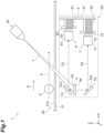
- FIG. 1 is a view showing a schematic configuration of an imaging system according to a first embodiment of the present disclosure.
- FIG. 2 is a plan view of an imaging unit shown in FIG. 1 .
- an imaging system 1 of the first embodiment is a device that acquires a radiation image of an object A.
- the imaging system 1 is an X-ray imaging system using a scintillator double-sided observation method.
- the imaging system 1 is applied to, for example, in-line X-ray inspection.
- the imaging system 1 shows good performance in discriminating, for example, a substance consisting of a light element.
- the imaging system 1 is applied to, for example, a field such as food inspection or battery inspection.
- the object A contains, for example, a substance consisting of a light element.
- a substance consisting of a light element In the field of food inspection, for example, it is inspected whether or not foreign matter is caught in food. Examples of such matter include food waste, hair, vinyl, insects, bones in meat, and the like.
- the imaging system 1 includes a conveying device 20 that conveys the object A in a predetermined conveying direction D (X-axis direction); a radiation source 30 that emits radiation L such as a white X-ray toward the object A conveyed by the conveying device 20; and an imaging unit 3A that executes image processing based on an image signal corresponding to the radiation L that has transmitted through the object A.
- a conveying device 20 that conveys the object A in a predetermined conveying direction D (X-axis direction)
- a radiation source 30 that emits radiation L such as a white X-ray toward the object A conveyed by the conveying device 20
- an imaging unit 3A that executes image processing based on an image signal corresponding to the radiation L that has transmitted through the object A.
- the conveying device 20 includes, for example, a belt conveyor 21 that moves on a revolving trajectory.
- the object A is placed or held on a conveying surface 21a of the belt conveyor 21.
- the belt conveyor 21 is a conveying stage or a conveying unit.
- the conveying device 20 includes a drive source (not shown) that drives the belt conveyor 21.
- the conveying device 20 is configured to convey the object A in the conveying direction D at a constant speed. In other words, the object A is conveyed on a predetermined conveying path P by the conveying device 20.
- the conveying direction D is a horizontal direction.
- the conveying path P has a linear shape.
- a direction in which the conveying path P extends is parallel to the conveying direction D.
- a conveying timing or a conveying speed of the object A in the conveying device 20 is set in advance and is controlled by a control unit.
- the imaging system 1 is compatible with the conveying device 20 of any form.
- the conveying direction D and the conveying path P may be horizontal.
- the conveying direction D and the conveying path P may be inclined with respect to the horizontal.
- the conveying path P may have a linear shape or a curved shape. In that case, the conveying direction D may be tangent to a portion of the conveying path P overlapping an irradiation region of the radiation.
- the conveying device 20 may not have the physical conveying surface 21a.
- the conveying device 20 may convey the object A in a state where the object A is lifted by the air.
- the conveying device 20 may convey the object A by releasing the object A to the air.
- the conveying path P may have, for example, a parabolic shape.
- the conveying device 20 may include a roller conveyor including a plurality of rollers.
- the radiation source 30 emits the radiation L.
- the radiation L is, for example, a cone beam X-ray.
- the radiation source 30 may be a microfocus X-ray source or a millifocus X-ray source.
- the radiation L emitted from the radiation source 30 forms a radiation flux.
- a presence region of the radiation flux is an emission region of the radiation source 30.
- the imaging unit 3A is disposed opposite the radiation source 30 with respect to the conveying surface 21a of the belt conveyor 21.
- the imaging unit 3A is attached to the conveying device 20 so as not to interfere with the revolving of the belt conveyor 21.
- the same also applies to the case where the conveying device 20 is a roller conveyor.
- the imaging unit 3A is disposed with some gap from the conveying unit so as not to interfere with movement of the conveying unit such as a belt conveyor, or a roller conveyor.
- the imaging unit 3A includes a scintillator 4, a first mirror 51, a second mirror 52, a first sensor module 6, a second sensor module 7, a processing substrate (image processing unit and control unit) 8, a first connection member 91, and a second connection member 92.
- the scintillator 4 is a wavelength conversion member.
- the scintillator 4 emits a scintillation light upon an incidence of the radiation L that has transmitted through the object A.
- the scintillator 4 has an oblong plate shape extending in a detection width direction (Y-axis direction).
- the scintillator 4 has a first surface 4a serving as an incident surface of the radiation L, and a second surface 4b facing the first surface 4a in a Z-axis direction.
- the first surface 4a and the second surface 4b are parallel to the conveying surface 21a of the belt conveyor 21.
- the first surface 4a faces a radiation source 30 side.
- the scintillator 4 converts the radiation L that has transmitted through the object A, into a scintillation light (visible light).
- An X-ray having a relatively low energy is converted into a scintillation light S1 by the first surface 4a of the scintillator 4, and the scintillation light S1 is output from the first surface 4a.
- an X-ray having a relatively high energy is converted into a scintillation light S2 by the second surface 4b of the scintillator 4, and the scintillation light S2 is output from the second surface 4b.
- the scintillator 4 consists of, for example, Gd 2 O 2 S:Tb, Gd 2 O 2 S:Pr, CsLTl, CdWO 4 , CaWO 4 , Gd 2 SiO 5 :Ce, Lu 0.4 Gd 1.6 SiO 5 , Bi 4 Ge 3 O 12 , Lu 2 SiO 5 :Ce, Y 2 SiO 5 , YAlO 3 :Ce, Y 2 O 2 S:Tb, YTaO 4 :Tm, YAG:Ce, YAG:Pr, YGAG:Ce, YGAG:Pr, GAGG:Ce, or the like.
- a thickness of the scintillator 4 is set to an appropriate value within a range of several ⁇ m to several mm depending on an energy band of radiation to be detected.
- the scintillator 4 may be formed of one scintillator.
- the scintillator 4 may be a combination of a plurality of scintillators. When the plurality of scintillators are combined, the types of the scintillators may be the same or different.
- the first mirror 51 is, for example, a mirror made of glass onto aluminum is evaporated or mirror-finished metal.
- the first mirror 51 is disposed on the radiation source 30 side with respect to the scintillator 4.
- the first mirror 51 has an oblong plate shape extending in the detection width direction (Y-axis direction).
- the first mirror 51 has a reflective surface 51a.
- the reflective surface 51a forms at an acute angle with respect to the first surface 4a of the scintillator 4.
- the reflective surface 51a obliquely faces the first surface 4a, and obliquely faces the first sensor module 6.
- the reflective surface 51a reflects the scintillation light S1 emitted from the first surface 4a, toward the first sensor module 6.
- the second mirror 52 is, for example, a mirror made of glass onto aluminum is evaporated or mirror-finished metal.
- the second mirror 52 is disposed opposite the first mirror 51 with respect to the scintillator 4.
- the second mirror 52 has an oblong plate shape extending in the detection width direction (Y-axis direction).
- the second mirror 52 has a reflective surface 52a.
- the reflective surface 52a forms at an acute angle with respect to the second surface 4b of the scintillator 4.
- the reflective surface 52a obliquely faces the second surface 4b, and obliquely faces the second sensor module 7.
- the reflective surface 52a reflects the scintillation light S2 emitted from the second surface 4b, toward the second sensor module 7.
- the reflective surface 51a has an area sufficient enough to reflect the scintillation light S1 emitted in a normal direction of the first surface 4a.
- the reflective surface 52a has an area sufficient enough to reflect the scintillation light S2 emitted in a normal direction of the second surface 4b. It is preferable that each of an angle between the reflective surface 51a and the first surface 4a and an angle between the reflective surface 52a and the second surface 4b is an angle within a range of 40 degrees or more 50 degrees or less. In the present embodiment, the angle is 45 degrees. The angle may be determined based on the disposition of the radiation source 30 or the position of a slit of a housing to be described later. Depending on the magnitude of the angle, the disposition of the first sensor module 6 and the second sensor module 7 may be appropriately adjusted.
- the first sensor module 6 is disposed apart from the scintillator 4 on one side (downstream side of the scintillator 4 in the conveying direction D) of the X-axis direction (in-plane direction of the first surface 4a and the second surface 4b of the scintillator 4).
- the first sensor module 6 is disposed on a first surface 4a side of the scintillator 4 in the Z-axis direction (facing direction between the first surface 4a and the second surface 4b of the scintillator 4).
- the first sensor module 6 detects the scintillation light S1 emitted from the first surface 4a upon an incidence of the radiation L, as a first scintillation light.
- the first scintillation light refers to a scintillation light detected by the first sensor module.
- the first sensor module 6 captures an image of the object A according to movement of the object A.
- the first sensor module 6 is a lens-coupled detector.
- the first sensor module 6 includes a first lens 61, a first body 62, and a first sensor 63.
- the first lens 61 is attached to the first body 62.
- the first lens 61 faces the reflective surface 51a of the first mirror 51 in the X-axis direction.
- An optical axis of the first lens 61 is parallel to the X-axis direction.
- the first lens 61 is focused on the reflective surface 51a.
- a visual field 61a of the first lens 61 extends over a wide range of the reflective surface 51a in the Y-axis direction.
- the first lens 61 condenses the scintillation light S1 reflected by the reflective surface 51a.
- the first sensor 63 is provided inside the first body 62. The first sensor 63 detects the scintillation light S1 condensed by the first lens 61, and outputs a first image signal corresponding to a detection result.
- the first sensor 63 is an image sensor.
- the first sensor 63 is, for example, a general line sensor, a multi-line sensor, or an area image sensor that can be driven in a time delay integration (TDI) mode.
- the first sensor 63 is, for example, a CCD area image sensor or a CMOS image sensor.
- the first sensor 63 has an element row along which a plurality of light-receiving elements are arranged in a row in a pixel direction.
- the image pitches of the plurality of light-receiving elements may be the same or different.
- a plurality of stages of the element rows are arranged in an integration direction to correspond to a movement direction of the object A.
- the first sensor 63 has a scanning direction corresponding to the conveying direction D of the object A, and a line direction orthogonal to the scanning direction.
- the scanning direction is the foregoing integration direction, and is parallel to the Z-axis direction.
- the line direction is the foregoing pixel direction, and is parallel to the Y-axis direction.
- the scanning direction is a direction that is converted from the conveying direction D via the first mirror 51. In the present embodiment, the scanning direction is converted from the conveying direction D by 90 degrees.
- the first sensor 63 is controlled by the control unit to perform charge transfer according to movement of the object A. Namely, the first sensor 63 performs charge transfer on a light receiving surface in synchronization with movement of the object A by the conveying device 20. Accordingly, a radiation image having a good S/N ratio can be obtained
- the control unit is configured to control the radiation source 30 and the first sensor module 6 to turn on the radiation source 30 according to an imaging timing of the first sensor module 6.
- the first sensor module 6 may be controlled by a signal from an encoder provided on a stage.
- the second sensor module 7 is disposed apart from the scintillator 4 on the one side in the X-axis direction.
- the second sensor module 7 is disposed on a second surface 4b side of the scintillator 4 in the Z-axis direction.
- the second sensor module 7 detects the scintillation light S2 emitted from the second surface 4b upon an incidence of the radiation L, as a second scintillation light.
- the second scintillation light refers to a scintillation light detected by the second sensor module.
- the second sensor module 7 captures an image of the object A according to movement of the object A.
- the second sensor module 7 is a lens-coupled detector.
- the second sensor module 7 includes a second lens 71, a second body 72, and a second sensor 73.
- the second lens 71 is attached to the second body 72.
- the second lens 71 faces the reflective surface 52a of the second mirror 52 in the X-axis direction.
- An optical axis of the second lens 71 is parallel to the X-axis direction.
- the second lens 71 is focused on the reflective surface 52a.
- a visual field 71a of the second lens 71 extends over a wide range of the reflective surface 52a in the Y-axis direction.
- the second lens 71 condenses the scintillation light S2 reflected by the reflective surface 52a.
- the second sensor 73 is provided inside the second body 72.
- the second sensor 73 detects the scintillation light S2 condensed by the second lens 71, and outputs a second image signal corresponding to a detection result.
- the second sensor 73 has the same configuration as that of the first sensor 63, and is controlled in the same manner as in the first sensor 63. A detailed description of the second sensor 73 will not be repeated.
- the processing substrate 8 includes a substrate 81 and a processor (not shown) attached to the substrate 81.
- the processing substrate 8 functions as an image processing unit that executes image processing based on the first image signal output from the first sensor 63 and on the second image signal output from the second sensor 73. Specifically, the processing substrate 8 performs image processing such as magnification correction, luminance value correction, dark correction, shading correction, affine transformation processing, edge enhancement processing, noise removal processing, bilateral filtering, or view angle adjustment on at least one of the first image signal and the second image signal.
- the processing substrate 8 outputs a radiation image created by executing the image processing, to a computer.
- the processing substrate 8 functions as a control unit that controls imaging conditions of the first sensor 63 and imaging conditions of the second sensor 73. Specifically, the processing substrate 8 sets an exposure time, a gain, an imaging frequency, an imaging timing, and the like for the first sensor 63 and the second sensor 73. In addition, the processing substrate 8 adjusts the imaging timing of the first sensor 63, the imaging timing of the second sensor 73, and image processing timing as the image processing unit and as the control unit. Accordingly, a process of causing the detection ranges of the first image signal and the second image signal to coincide with each other and a process of such as comparing or combining the first image signal and the second image signal are facilitated. The processing substrate 8 may perform control to delay the output of at least one of the first image signal and the second image signal within a range more than the exposure time.
- one processing substrate 8 is provided for the first sensor module 6 and the second sensor module 7. Namely, the processing substrate 8 is common to the first sensor module 6 and the second sensor module 7.
- the first connection member 91 electrically connects the first sensor module 6 and the processing substrate 8. Specifically, the first connection member 91 electrically connects the first sensor 63 and the image processing processor via wirings provided on the first body 62 and via wirings provided on the substrate 81.
- the second connection member 92 electrically connects the second sensor module 7 and the processing substrate 8. Specifically, the second connection member 92 electrically connects the second sensor 73 and the image processing processor via wirings provided on the second body 72 and via wirings provided on the substrate 81. Accordingly, the first image signal and the second image signal can be output to the processing substrate 8.
- Each of the first connection member 91 and the second connection member 92 has flexibility. Each of the first connection member 91 and the second connection member 92 is easily deformable to the extent that the first connection member 91 and the second connection member 92 receive a load corresponding to, for example, a force of worker's fingers.
- Each of the first connection member 91 and the second connection member 92 is formed of, for example, a cable, a connector, and the like.
- Each of the first connection member 91 and the second connection member 92 is formed of, for example, a harness, a connector, and the like.
- Each of the first connection member 91 and the second connection member 92 is, for example, a flexible connector.
- the imaging unit 3A includes, for example, a housing (not shown) having a rectangular parallelepiped shape.
- the scintillator 4, the first mirror 51, the second mirror 52, the first sensor module 6, the second sensor module 7, and the processing substrate 8 are housed in the housing.
- Each of the scintillator 4, the first mirror 51, the second mirror 52, the first sensor module 6, the second sensor module 7, and the processing substrate 8 is held by the housing.
- a slit through which the radiation L emitted from the radiation source 30 passes is formed in a wall portion on the radiation source 30 side of the housing.
- the slit has, for example, an oblong shape extending in the detection width direction (Y-axis direction).
- the housing is made of, for example, a material capable of blocking X-rays.
- the housing is a so-called dark box.
- the housing may be made of, for example, metal.
- the housing is made of, for example, aluminum, iron, stainless steel, or the like.
- the housing may contain a protective material.
- the protective material is, for example, metal. Examples of the protective material include lead, tungsten, copper, iron, stainless steel, and the like.
- the housing has a shape that is long in the conveying direction D. The housing may be attached to the conveying device 20.
- the imaging system 1 includes the control unit (not shown).
- the control unit controls the radiation source 30 based on a value of a tube voltage or a tube current of the radiation source 30 stored by a user's input or the like.
- the control unit controls each of the first sensor module 6 and the second sensor module 7 based on the exposure time and the like of each of the first sensor module 6 and the second sensor module 7 stored by a user's input or the like.
- the control unit and the image processing processor of the processing substrate 8 may be separate processors or the same processor.
- An interval between the reflective surface 51a and the first surface 4a of the scintillator 4 in the Z-axis direction is smaller than an interval between the reflective surface 52a and the second surface 4b of the scintillator 4 in the Z-axis direction.
- an optical path length of the scintillation light S1 in the Z-axis direction between the reflective surface 51a and the first surface 4a is smaller than an optical path length of the scintillation light S2 in the Z-axis direction between the reflective surface 52a and the second surface 4b.
- An interval between the first lens 61 and the first surface 4a of the scintillator 4 in the Z-axis direction is smaller than an interval between the second lens 71 and the second surface 4b of the scintillator 4 in the Z-axis direction.
- an interval between the optical axis of the first lens 61 and the first surface 4a is smaller than an interval between the optical axis of the second lens 71 and the second surface 4b.
- a position of the second lens 71 in the X-axis direction is closer to a scintillator 4 side than a position of the first lens 61 in the X-axis direction.
- an optical path length of the scintillation light S2 in the X-axis direction between the reflective surface 52a and the second lens 71 is smaller than an optical path length of the scintillation light S1 in the X-axis direction between the reflective surface 51a and the first lens 61.
- An optical path length of the scintillation light S1 between the first surface 4a of the scintillator 4 and the first lens 61 is equal to an optical path length of the scintillation light S2 between the second surface 4b of the scintillator 4 and the second lens 71.
- the sum of the optical path length of the scintillation light S1 in the Z-axis direction between the reflective surface 51a and the first surface 4a and the optical path length of the scintillation light S1 in the X-axis direction between the reflective surface 51a and the first lens 61 is equal to the sum of the optical path length of the scintillation light S2 in the Z-axis direction between the reflective surface 52a and the second surface 4b and the optical path length of the scintillation light S2 in the X-axis direction between the reflective surface 52a and the second lens 71.
- the first mirror 51 and the first sensor module 6 are disposed close to the scintillator 4 in the Z-axis direction, and the optical path length of the scintillation light S1 and the scintillation light S2 are set to coincide with each other. Accordingly, the scintillator 4 can be disposed close to the object A, and a radiation image of the object A can be accurately acquired.
- each of the first connection member 91 and the second connection member 92 has flexibility. Namely, the first sensor module 6 and the second sensor module 7 are connected to the processing substrate 8 by the first connection member 91 and the second connection member 92, and the positions thereof with respect to the processing substrate 8 can be adjusted. Accordingly, the above-described positional relationship can be easily adjusted by adjusting the position of each of the first sensor module 6 and the second sensor module 7.
- the object A is conveyed in the conveying direction D by the conveying device 20.
- the radiation source 30 emits the radiation L toward the object A.
- the radiation L that has transmitted through the object A is incident on the first surface 4a.
- the radiation L is converted into a scintillation light by the scintillator 4.
- the scintillation light S1 emitted from the first surface 4a is reflected by the first mirror 51, and is imaged on the first sensor 63 by the first lens 61 of the first sensor module 6.
- the first sensor 63 captures an image of the scintillation light S1 (scintillation image) imaged by the first lens 61.
- the first sensor module 6 outputs the radiation image data (first image signal) obtained by imaging, to the processing substrate 8.
- the second sensor module 7 captures an image of the scintillation light S2, and outputs the obtained radiation image data (second image signal) to the processing substrate 8.
- the radiation image data is input to the processing substrate 8, and the processing substrate 8 executes predetermined processing such as image processing on the input radiation image data to create a radiation image.
- the processing substrate 8 outputs the created radiation image to the computer.
- the computer displays the radiation image output from the processing substrate 8. As described above, the radiation image is obtained by double-sided observation of the object A.
- the processing substrate 8 that processes the first image signal and the second image signal from the first sensor module 6 and the second sensor module 7 is common. Therefore, the configuration is simplified compared to a configuration in which a processing substrate is provided for each sensor module.
- each of the first connection member 91 and the second connection member 92 that connect the first sensor module 6 and the second sensor module 7 to the processing substrate 8, respectively has flexibility for common use of the processing substrate 8. For this reason, the imaging positions of the first sensor module 6 and the second sensor module 7 can be separately adjusted, and the degree of freedom in adjusting the imaging positions can be sufficiently ensured.
- the imaging unit 3A includes the scintillator 4 that emits the scintillation lights S1 and S2 upon an incidence of the radiation L. Accordingly, workability when the imaging unit 3A is assembled to the imaging system 1 can be improved.
- the scintillator 4 has the first surface 4a serving as an incident surface of the radiation L, and the second surface 4b facing the first surface 4a.
- the first sensor module 6 is disposed on the first surface 4a side of the scintillator 4 in the Z-axis direction.
- the first sensor module 6 detects the scintillation light S1 emitted from the first surface 4a upon an incidence of the radiation L, as the first scintillation light.
- the second sensor module 7 is disposed on the second surface 4b side of the scintillator 4 in the Z-axis direction.
- the second sensor module 7 detects the scintillation light S2 emitted from the second surface 4b upon an incidence of the radiation L, as the second scintillation light. Accordingly, for example, dual-energy imaging using a scintillation light in a low energy band and a scintillation light in a high energy band can be suitably realized.
- the first sensor module 6 and the second sensor module 7 are disposed apart from the scintillator 4 on the one side in the X-axis direction.
- the interval between the first lens 61 of the first sensor module 6 and the first surface 4a in the Z-axis direction is smaller than the interval between the second lens 71 of the second sensor module 7 and the second surface 4b in the Z-axis direction.
- the position of the second lens 71 in the X-axis direction is closer to the scintillator 4 side than the position of the first lens 61 in the Z-axis direction. Accordingly, when the imaging unit 3A is assembled to the imaging system 1, the first surface 4a of the scintillator 4 can be disposed close to the object A.
- the optical path length of the scintillation light S1 (first scintillation light) and the optical path length of the scintillation light S2 (second scintillation light) can be set to coincide with each other.
- the configuration can be simplified, and the degree of freedom in adjusting the imaging positions can be sufficiently ensured.
- FIG. 3 is a view showing a schematic configuration of an imaging unit according to a second embodiment of the present disclosure.
- FIG. 4 is a plan view of the imaging unit shown in FIG. 3 .
- an imaging unit 3B according to the second embodiment differs from the imaging unit 3A of the first embodiment in that the first sensor module 6 and the second sensor module 7 are disposed on the first surface 4a side of the scintillator 4 and are arranged in the Y-axis direction and the second mirror 52 is not provided.
- An imaging system is an X-ray imaging system using a scintillator front surface observation method.
- the first sensor module 6 and the second sensor module 7 are disposed on the first surface 4a side of the scintillator 4 in the Z-axis direction, and are arranged in the Y-axis direction (in-plane direction of the first surface 4a).
- the first sensor module 6 detects the scintillation light S1 emitted from the first surface 4a upon an incidence of the radiation L, as a first scintillation light.
- the second sensor module 7 detects the scintillation light S1 emitted from the first surface 4a upon an incidence of the radiation L, as a second scintillation light.
- An interval between the first lens 61 of the first sensor module 6 and the scintillator 4 in the Z-axis direction is equal to an interval between the second lens 71 of the second sensor module 7 and the scintillator 4 in the Z-axis direction.
- an interval between the optical axis of the first lens 61 and the first surface 4a is equal to an interval between the optical axis of the second lens 71 and the first surface 4a.
- an optical path length of the scintillation light S1 (the scintillation light S1 to be incident on the first lens 61) in the Z-axis direction between the reflective surface 51a of the first mirror 51 and the first surface 4a is equal to an optical path length of the scintillation light S1 (the scintillation light S1 to be incident on the second lens 71) in the Z-axis direction between the reflective surface 51a and the first surface 4a.
- an optical path length of the scintillation light S1 in the X-axis direction between the reflective surface 51a and the first lens 61 is equal to an optical path length of the scintillation light S1 in the X-axis direction between the reflective surface 51a and the second lens 71.
- an optical path length of the scintillation light S1 between the first surface 4a of the scintillator 4 and the first lens 61 is equal to an optical path length of the scintillation light S1 between the first surface 4a of the scintillator 4 and the second lens 71.
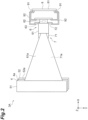
- FIG. 5 is a view showing visual fields of the first lens 61 and the second lens 71 shown in FIG. 3 .
- the first mirror 51 is not shown.
- the visual fields of the first lens 61 and the second lens 71 partially overlap each other in the Y-axis direction.
- the range of the visual field 61a of the first lens 61 in the Y-axis direction with respect to the first surface 4a and the range of the visual field 61a of the second lens 71 in the Y-axis direction with respect to the first surface 4a partially overlap each other.
- the range of the visual field 61a of the first lens 61 in the Y-axis direction and the range of the visual field 71a of the second lens 71 in the Y-axis direction partially overlap each other on the reflective surface 51a (refer to FIG. 3 ) of the first mirror 51.
- An overlapping region R exists between the visual field 61a and the visual field 71a.
- a width of the overlapping region R in the Y-axis direction can be adjusted by adjusting the positions of the first sensor module 6 and the second sensor module 7 in the Y-axis direction.
- the first sensor module 6 and the second sensor module 7 are arranged in the Y-axis direction, so that a visual field of the imaging unit 3B in the Y-axis direction is widened, and the overlapping region R is appropriately provided, so that the visual field 61a and the visual field 71a are continuous with each other in the Y-axis direction.
- the first connection member 91 and the second connection member 92 have flexibility, the position of each of the first sensor module 6 and the second sensor module 7 with respect to the processing substrate 8 can be adjusted. Accordingly, the above-described positional relationship can be easily adjusted by adjusting the position of each of the first sensor module 6 and the second sensor module 7.
- the scintillator 4 has the first surface 4a serving as an incident surface of the radiation L, and the second surface 4b facing the first surface 4a.
- the first sensor module 6 and the second sensor module 7 are disposed on the first surface 4a side of the scintillator 4 in the Z-axis direction, and are arranged in the Y-axis direction.
- the first sensor module 6 detects the scintillation light S1 emitted from the first surface 4a upon an incidence of the radiation L, as the first scintillation light.
- the second sensor module 7 detects the scintillation light S1 emitted from the first surface 4a upon an incidence of the radiation L, as the second scintillation light. Accordingly, the respective scintillation lights S1 from single side of the scintillator 4 can be accurately detected by the first sensor module 6 and the second sensor module 7.
- the visual field 61a of the first lens 61 of the first sensor module 6 and the visual field 71a of the second lens 71 of the second sensor module 7 partially overlap each other in the Z-axis direction. Accordingly, the visual field 61a of the first lens 61 and the visual field 71a of the second lens 71 are continuous with each other, and an image of the scintillation light S1 can be captured over a wide range without a blind spot.
- the first sensor module 6 and the second sensor module 7 are disposed apart from the scintillator 4 on the one side in the X-axis direction.
- the interval between the first lens 61 of the first sensor module 6 and the scintillator 4 in the Z-axis direction is equal to the interval between the second lens 71 of the second sensor module 7 and the scintillator 4 in the Z-axis direction.
- the positions of the first lens 61 and the second lens 71 in the X-axis direction with respect to the scintillator 4 coincide with each other. Accordingly, the first lens 61 and the second lens 71 can be common.
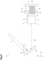
- FIG. 6 is a view showing a schematic configuration of an imaging unit according to a third embodiment of the present disclosure.
- FIG. 7 is a plan view of the imaging unit shown in FIG. 6 .
- an imaging unit 3C according to the third embodiment differs from the imaging unit 3B of the second embodiment in that the first sensor module 6 and the second sensor module 7 are disposed on the second surface 4b side of the scintillator 4, and in that the first mirror 51 is not provided and the second mirror 52 is provided.
- An imaging system is an X-ray imaging system using a scintillator back surface observation method.
- the first sensor module 6 and the second sensor module 7 are disposed on the second surface 4b side of the scintillator 4 in the Z-axis direction.
- the first sensor module 6 detects the scintillation light S2 emitted from the second surface 4b upon an incidence of the radiation L, as a first scintillation light.
- the second sensor module 7 detects the scintillation light S2 emitted from the second surface 4b upon an incidence of the radiation L, as a second scintillation light.
- an interval between the optical axis of the first lens 61 and the second surface 4b is equal to an interval between the optical axis of the second lens 71 and the second surface 4b, and the positions of the first lens 61 and the second lens 71 in the X-axis direction with respect to the scintillator 4 coincide with each other.
- the visual fields of the first lens 61 and the second lens 71 partially overlap each other in the Y-axis direction.
- the scintillator 4 has the first surface 4a serving as an incident surface of the radiation L, and the second surface 4b facing the first surface 4a.
- the first sensor module 6 and the second sensor module 7 are disposed on the second surface 4b side of the scintillator 4 in the Z-axis direction, and are arranged in the Y-axis direction.
- the first sensor module 6 detects the scintillation light S2 emitted from the second surface 4b upon an incidence of the radiation L, as the first scintillation light.
- the second sensor module 7 detects the scintillation light S2 emitted from the second surface 4b upon an incidence of the radiation L, as the second scintillation light. Accordingly, the respective scintillation lights S2 from single side of the scintillator 4 can be accurately detected by the first sensor module 6 and the second sensor module 7.
- the imaging units 3A, 3B, and 3C include the scintillator 4, but the imaging units 3A, 3B, and 3C may not include the scintillator 4.
- the scintillator 4 may not be a configuration of the imaging units 3A, 3B, and 3C.
- the scintillator 4 may be a configuration of the imaging system.
- imaging system 3A, 3B, 3C: imaging unit
- 4 scintillator
- 4a first surface
- 4b second surface
- 6 first sensor module
- 7 second sensor module
- 8 processing substrate
- 20 conveying device
- 30 radiation source
- 61 first lens
- 61a visual field
- 63 first sensor
- 71 second lens
- 73 second sensor
- 91 first connection member
- 92 second connection member
- A object
- L radiation
- S1, S2 scintillation light.
Abstract
An imaging unit includes: a first sensor module; a second sensor module; a processing substrate; a first connection member; and a second connection member. The first sensor module includes a first lens and a first sensor. The second sensor module includes a second lens and a second sensor. The processing substrate executes image processing based on the first image signal and the second image signal. The first connection member electrically connects the first sensor module and the processing substrate, and has flexibility. The second connection member electrically connects the second sensor module and the processing substrate, and has flexibility.
Description
- The present disclosure relates to an imaging unit and an imaging system.
- As an imaging system of the related art, for example, there is an imaging system described in
Patent Literature 1. The imaging system of the related art includes a first sensor module and a second sensor module that detect scintillation lights emitted from a scintillator. The first sensor module and the second sensor module capture images of respective scintillation lights emitted from a front surface and a back surface of the scintillator. Accordingly, dual-energy imaging for acquiring radiation images of an object in different energy bands is realized. - Patent Literature 1:
Japanese Unexamined Patent Publication No. 2012-154733 - In the imaging system above described, since a plurality of sensor modules are used, it is considered that a configuration of an imaging unit forming the imaging system becomes complicated. In addition, in the imaging system described above, there may be restrictions on the disposition of the scintillator to optimize imaging of the object. In that case, ensuring the degree of freedom in adjusting imaging positions in the imaging unit is required.
- An object of the present disclosure is to provide an imaging unit and an imaging system capable of ensuring the degree of freedom in adjusting imaging positions with a simple configuration.
- An imaging unit according to one aspect of the present disclosure includes: a first sensor module; a second sensor module; a processing substrate; a first connection member; and a second connection member. The first sensor module includes a first lens that condenses a first scintillation light, and a first sensor that detects the first scintillation light condensed by the first lens, and that outputs a first image signal corresponding to a detection result. The second sensor module includes a second lens that condenses a second scintillation light, and a second sensor that detects the second scintillation light condensed by the second lens, and that outputs a second image signal corresponding to a detection result. The processing substrate executes image processing based on the first image signal and the second image signal. The first connection member electrically connects the first sensor module and the processing substrate, and has flexibility. The second connection member electrically connects the second sensor module and the processing substrate, and has flexibility.
- In the imaging unit, the processing substrate that processes the first image signal and the second image signal from the first sensor module and the second sensor module is common. Therefore, the configuration is simplified compared to a configuration in which a processing substrate is provided for each sensor module. In addition, in the imaging unit, each of the first connection member and the second connection member that connect the first sensor module and the second sensor module to the processing substrate, respectively, has flexibility for common use of the processing substrate. For this reason, the imaging positions of the first sensor module and the second sensor module can be separately adjusted. Therefore, the degree of freedom in adjusting the imaging positions can be sufficiently ensured.
- The imaging unit may further include a scintillator that emits a scintillation light upon an incidence of radiation. Accordingly, workability when the imaging unit is assembled to an imaging system can be improved.
- The scintillator may have a first surface serving as an incident surface of the radiation, and a second surface facing the first surface. The first sensor module may be disposed on a first surface side of the scintillator in a facing direction between the first surface and the second surface. The first sensor module may detect the scintillation light emitted from the first surface upon the incidence of the radiation, as the first scintillation light. The second sensor module may be disposed on a second surface side of the scintillator in the facing direction. The second sensor module may detect the scintillation light emitted from the second surface upon the incidence of the radiation, as the second scintillation light. Accordingly, for example, dual-energy imaging using a scintillation light in a low energy band and a scintillation light in a high energy band can be suitably realized.
- The first sensor module and the second sensor module may be disposed apart from the scintillator on one side in an in-plane direction of the first surface and the second surface. An interval between the first lens of the first sensor module and the first surface in the facing direction may be smaller than an interval between the second lens of the second sensor module and the second surface in the facing direction. A position of the second lens in the in-plane direction may be closer to a scintillator side than a position of the first lens in the in-plane direction. In this case, when the imaging unit is assembled to the imaging system, the first surface of the scintillator can be disposed close to an object. In addition, even when the first surface of the scintillator is disposed close to the object, an optical path length of the first scintillation light and an optical path length of the second scintillation light can be set to coincide with each other.
- The scintillator may have a first surface serving as an incident surface of the radiation, and a second surface facing the first surface. The first sensor module and the second sensor module may be disposed on a first surface side of the scintillator in a facing direction between the first surface and the second surface, and may be arranged in an in-plane direction of the first surface. The first sensor module may detect the scintillation light emitted from the first surface upon the incidence of the radiation, as the first scintillation light. The second sensor module may detect the scintillation light emitted from the first surface upon the incidence of the radiation, as the second scintillation light. In this case, the respective scintillation lights from single side of the scintillator can be accurately detected by the first sensor module and the second sensor module.
- The scintillator may have a first surface serving as an incident surface of the radiation, and a second surface facing the first surface. The first sensor module and the second sensor module may be disposed on a second surface side of the scintillator in a facing direction between the first surface and the second surface, and may be arranged in an in-plane direction of the second surface. The first sensor module may detect the scintillation light emitted from the second surface upon the incidence of the radiation, as the first scintillation light. The second sensor module may detect the scintillation light emitted from the second surface upon the incidence of the radiation, as the second scintillation light. In this case, the respective scintillation lights from single side of the scintillator can be accurately detected by the first sensor module and the second sensor module.
- A visual field of the first lens of the first sensor module and a visual field of the second lens of the second sensor module may partially overlap each other in the in-plane direction of the first surface and the second surface. In this case, since the visual field of the first lens and the visual field of the second lens are continuous with each other, an image of the scintillation light can be captured over a wide range without a blind spot.
- The first sensor module and the second sensor module may be disposed apart from the scintillator on one side in the in-plane direction of the first surface and the second surface. An interval between the first lens of the first sensor module and the scintillator in the facing direction may be equal to an interval between the second lens of the second sensor module and the scintillator in the facing direction. Positions of the first lens and the second lens in the in-plane direction with respect to the scintillator may coincide with each other. In this case, the first lens and the second lens can be common. In addition, since image correction due to a difference between the optical path length of the first scintillation light to be incident on the first lens and the optical path length of the second scintillation light to be incident on the second lens is not required, image processing in the processing substrate can be prevented from being complicated.
- An imaging system according to one aspect of the present disclosure includes: a conveying device that conveys an object; a radiation source that emits radiation toward the object conveyed by the conveying device; and the imaging unit that executes image processing based on an image signal corresponding to the radiation that has transmitted through the object. According to the imaging system, as described above, the configuration can be simplified, and the degree of freedom in adjusting imaging positions can be sufficiently ensured.
- According to the present disclosure, it is possible to provide the imaging unit and the imaging system capable of ensuring the degree of freedom in adjusting the imaging positions with a simple configuration.
-
-
FIG. 1 is a view showing a schematic configuration of an imaging system according to a first embodiment. -
FIG. 2 is a plan view of an imaging unit shown inFIG. 1 . -
FIG. 3 is a view showing a schematic configuration of an imaging unit according to a second embodiment. -
FIG. 4 is a plan view of the imaging unit shown inFIG. 3 . -
FIG. 5 is a view showing visual fields of a first lens and a second lens shown inFIG. 3 . -
FIG. 6 is a view showing a schematic configuration of an imaging unit according to a third embodiment. -
FIG. 7 is a plan view of the imaging unit shown inFIG. 6 . - Hereinafter, embodiments of the present disclosure will be described with reference to the drawings. In the description of the drawings, the same elements are denoted by the same reference signs, and duplicate descriptions will not be repeated. In addition, in each drawing, for convenience of description, portions to be described are drawn in an emphasized manner. For this reason, a dimensional ratio of each member in the drawings does not necessarily coincide with an actual dimensional ratio.
- [First embodiment]
FIG. 1 is a view showing a schematic configuration of an imaging system according to a first embodiment of the present disclosure.FIG. 2 is a plan view of an imaging unit shown inFIG. 1 . As shown inFIGS. 1 and2 , animaging system 1 of the first embodiment is a device that acquires a radiation image of an object A. Theimaging system 1 is an X-ray imaging system using a scintillator double-sided observation method. Theimaging system 1 is applied to, for example, in-line X-ray inspection. Theimaging system 1 shows good performance in discriminating, for example, a substance consisting of a light element. Theimaging system 1 is applied to, for example, a field such as food inspection or battery inspection. The object A contains, for example, a substance consisting of a light element. In the field of food inspection, for example, it is inspected whether or not foreign matter is caught in food. Examples of such matter include food waste, hair, vinyl, insects, bones in meat, and the like. - The
imaging system 1 includes a conveyingdevice 20 that conveys the object A in a predetermined conveying direction D (X-axis direction); aradiation source 30 that emits radiation L such as a white X-ray toward the object A conveyed by the conveyingdevice 20; and animaging unit 3A that executes image processing based on an image signal corresponding to the radiation L that has transmitted through the object A. - The conveying
device 20 includes, for example, abelt conveyor 21 that moves on a revolving trajectory. The object A is placed or held on a conveyingsurface 21a of thebelt conveyor 21. Thebelt conveyor 21 is a conveying stage or a conveying unit. The conveyingdevice 20 includes a drive source (not shown) that drives thebelt conveyor 21. The conveyingdevice 20 is configured to convey the object A in the conveying direction D at a constant speed. In other words, the object A is conveyed on a predetermined conveying path P by the conveyingdevice 20. In the present embodiment, the conveying direction D is a horizontal direction. In addition, the conveying path P has a linear shape. A direction in which the conveying path P extends is parallel to the conveying direction D. A conveying timing or a conveying speed of the object A in the conveyingdevice 20 is set in advance and is controlled by a control unit. - The
imaging system 1 is compatible with the conveyingdevice 20 of any form. The conveying direction D and the conveying path P may be horizontal. The conveying direction D and the conveying path P may be inclined with respect to the horizontal. The conveying path P may have a linear shape or a curved shape. In that case, the conveying direction D may be tangent to a portion of the conveying path P overlapping an irradiation region of the radiation. The conveyingdevice 20 may not have the physical conveyingsurface 21a. The conveyingdevice 20 may convey the object A in a state where the object A is lifted by the air. The conveyingdevice 20 may convey the object A by releasing the object A to the air. In that case, the conveying path P may have, for example, a parabolic shape. The conveyingdevice 20 may include a roller conveyor including a plurality of rollers. - The
radiation source 30 emits the radiation L. The radiation L is, for example, a cone beam X-ray. Theradiation source 30 may be a microfocus X-ray source or a millifocus X-ray source. The radiation L emitted from theradiation source 30 forms a radiation flux. A presence region of the radiation flux is an emission region of theradiation source 30. - The
imaging unit 3A is disposed opposite theradiation source 30 with respect to the conveyingsurface 21a of thebelt conveyor 21. Theimaging unit 3A is attached to the conveyingdevice 20 so as not to interfere with the revolving of thebelt conveyor 21. The same also applies to the case where the conveyingdevice 20 is a roller conveyor. Theimaging unit 3A is disposed with some gap from the conveying unit so as not to interfere with movement of the conveying unit such as a belt conveyor, or a roller conveyor. - The
imaging unit 3A includes ascintillator 4, afirst mirror 51, asecond mirror 52, afirst sensor module 6, asecond sensor module 7, a processing substrate (image processing unit and control unit) 8, afirst connection member 91, and asecond connection member 92. - The
scintillator 4 is a wavelength conversion member. Thescintillator 4 emits a scintillation light upon an incidence of the radiation L that has transmitted through the object A. Thescintillator 4 has an oblong plate shape extending in a detection width direction (Y-axis direction). Thescintillator 4 has afirst surface 4a serving as an incident surface of the radiation L, and asecond surface 4b facing thefirst surface 4a in a Z-axis direction. Thefirst surface 4a and thesecond surface 4b are parallel to the conveyingsurface 21a of thebelt conveyor 21. Thefirst surface 4a faces aradiation source 30 side. Thescintillator 4 converts the radiation L that has transmitted through the object A, into a scintillation light (visible light). An X-ray having a relatively low energy is converted into a scintillation light S1 by thefirst surface 4a of thescintillator 4, and the scintillation light S1 is output from thefirst surface 4a. In addition, an X-ray having a relatively high energy is converted into a scintillation light S2 by thesecond surface 4b of thescintillator 4, and the scintillation light S2 is output from thesecond surface 4b. - The
scintillator 4 consists of, for example, Gd2O2S:Tb, Gd2O2S:Pr, CsLTl, CdWO4, CaWO4, Gd2SiO5:Ce, Lu0.4Gd1.6SiO5, Bi4Ge3O12, Lu2SiO5:Ce, Y2SiO5, YAlO3:Ce, Y2O2S:Tb, YTaO4:Tm, YAG:Ce, YAG:Pr, YGAG:Ce, YGAG:Pr, GAGG:Ce, or the like. A thickness of thescintillator 4 is set to an appropriate value within a range of several µm to several mm depending on an energy band of radiation to be detected. Thescintillator 4 may be formed of one scintillator. Thescintillator 4 may be a combination of a plurality of scintillators. When the plurality of scintillators are combined, the types of the scintillators may be the same or different. - The
first mirror 51 is, for example, a mirror made of glass onto aluminum is evaporated or mirror-finished metal. Thefirst mirror 51 is disposed on theradiation source 30 side with respect to thescintillator 4. Thefirst mirror 51 has an oblong plate shape extending in the detection width direction (Y-axis direction). Thefirst mirror 51 has areflective surface 51a. Thereflective surface 51a forms at an acute angle with respect to thefirst surface 4a of thescintillator 4. Thereflective surface 51a obliquely faces thefirst surface 4a, and obliquely faces thefirst sensor module 6. Thereflective surface 51a reflects the scintillation light S1 emitted from thefirst surface 4a, toward thefirst sensor module 6. - The
second mirror 52 is, for example, a mirror made of glass onto aluminum is evaporated or mirror-finished metal. Thesecond mirror 52 is disposed opposite thefirst mirror 51 with respect to thescintillator 4. Thesecond mirror 52 has an oblong plate shape extending in the detection width direction (Y-axis direction). Thesecond mirror 52 has areflective surface 52a. Thereflective surface 52a forms at an acute angle with respect to thesecond surface 4b of thescintillator 4. Thereflective surface 52a obliquely faces thesecond surface 4b, and obliquely faces thesecond sensor module 7. Thereflective surface 52a reflects the scintillation light S2 emitted from thesecond surface 4b, toward thesecond sensor module 7. - The
reflective surface 51a has an area sufficient enough to reflect the scintillation light S1 emitted in a normal direction of thefirst surface 4a. Thereflective surface 52a has an area sufficient enough to reflect the scintillation light S2 emitted in a normal direction of thesecond surface 4b. It is preferable that each of an angle between thereflective surface 51a and thefirst surface 4a and an angle between thereflective surface 52a and thesecond surface 4b is an angle within a range of 40 degrees or more 50 degrees or less. In the present embodiment, the angle is 45 degrees. The angle may be determined based on the disposition of theradiation source 30 or the position of a slit of a housing to be described later. Depending on the magnitude of the angle, the disposition of thefirst sensor module 6 and thesecond sensor module 7 may be appropriately adjusted. - The
first sensor module 6 is disposed apart from thescintillator 4 on one side (downstream side of thescintillator 4 in the conveying direction D) of the X-axis direction (in-plane direction of thefirst surface 4a and thesecond surface 4b of the scintillator 4). Thefirst sensor module 6 is disposed on afirst surface 4a side of thescintillator 4 in the Z-axis direction (facing direction between thefirst surface 4a and thesecond surface 4b of the scintillator 4). Thefirst sensor module 6 detects the scintillation light S1 emitted from thefirst surface 4a upon an incidence of the radiation L, as a first scintillation light. Incidentally, the first scintillation light refers to a scintillation light detected by the first sensor module. - The
first sensor module 6 captures an image of the object A according to movement of the object A. Thefirst sensor module 6 is a lens-coupled detector. Specifically, thefirst sensor module 6 includes afirst lens 61, afirst body 62, and afirst sensor 63. Thefirst lens 61 is attached to thefirst body 62. Thefirst lens 61 faces thereflective surface 51a of thefirst mirror 51 in the X-axis direction. An optical axis of thefirst lens 61 is parallel to the X-axis direction. Thefirst lens 61 is focused on thereflective surface 51a. Avisual field 61a of thefirst lens 61 extends over a wide range of thereflective surface 51a in the Y-axis direction. Thefirst lens 61 condenses the scintillation light S1 reflected by thereflective surface 51a. Thefirst sensor 63 is provided inside thefirst body 62. Thefirst sensor 63 detects the scintillation light S1 condensed by thefirst lens 61, and outputs a first image signal corresponding to a detection result. - The
first sensor 63 is an image sensor. Thefirst sensor 63 is, for example, a general line sensor, a multi-line sensor, or an area image sensor that can be driven in a time delay integration (TDI) mode. Thefirst sensor 63 is, for example, a CCD area image sensor or a CMOS image sensor. Thefirst sensor 63 has an element row along which a plurality of light-receiving elements are arranged in a row in a pixel direction. The image pitches of the plurality of light-receiving elements may be the same or different. In thefirst sensor 63, a plurality of stages of the element rows are arranged in an integration direction to correspond to a movement direction of the object A. Thefirst sensor 63 has a scanning direction corresponding to the conveying direction D of the object A, and a line direction orthogonal to the scanning direction. The scanning direction is the foregoing integration direction, and is parallel to the Z-axis direction. The line direction is the foregoing pixel direction, and is parallel to the Y-axis direction. The scanning direction is a direction that is converted from the conveying direction D via thefirst mirror 51. In the present embodiment, the scanning direction is converted from the conveying direction D by 90 degrees. - The
first sensor 63 is controlled by the control unit to perform charge transfer according to movement of the object A. Namely, thefirst sensor 63 performs charge transfer on a light receiving surface in synchronization with movement of the object A by the conveyingdevice 20. Accordingly, a radiation image having a good S/N ratio can be obtained When thefirst sensor 63 is an area image sensor, the control unit is configured to control theradiation source 30 and thefirst sensor module 6 to turn on theradiation source 30 according to an imaging timing of thefirst sensor module 6. Thefirst sensor module 6 may be controlled by a signal from an encoder provided on a stage. - The
second sensor module 7 is disposed apart from thescintillator 4 on the one side in the X-axis direction. Thesecond sensor module 7 is disposed on asecond surface 4b side of thescintillator 4 in the Z-axis direction. Thesecond sensor module 7 detects the scintillation light S2 emitted from thesecond surface 4b upon an incidence of the radiation L, as a second scintillation light. Incidentally, the second scintillation light refers to a scintillation light detected by the second sensor module. - The
second sensor module 7 captures an image of the object A according to movement of the object A. Thesecond sensor module 7 is a lens-coupled detector. Specifically, thesecond sensor module 7 includes asecond lens 71, asecond body 72, and asecond sensor 73. Thesecond lens 71 is attached to thesecond body 72. Thesecond lens 71 faces thereflective surface 52a of thesecond mirror 52 in the X-axis direction. An optical axis of thesecond lens 71 is parallel to the X-axis direction. Thesecond lens 71 is focused on thereflective surface 52a. Avisual field 71a of thesecond lens 71 extends over a wide range of thereflective surface 52a in the Y-axis direction. Thesecond lens 71 condenses the scintillation light S2 reflected by thereflective surface 52a. Thesecond sensor 73 is provided inside thesecond body 72. Thesecond sensor 73 detects the scintillation light S2 condensed by thesecond lens 71, and outputs a second image signal corresponding to a detection result. Thesecond sensor 73 has the same configuration as that of thefirst sensor 63, and is controlled in the same manner as in thefirst sensor 63. A detailed description of thesecond sensor 73 will not be repeated. - The
processing substrate 8 includes asubstrate 81 and a processor (not shown) attached to thesubstrate 81. Theprocessing substrate 8 functions as an image processing unit that executes image processing based on the first image signal output from thefirst sensor 63 and on the second image signal output from thesecond sensor 73. Specifically, theprocessing substrate 8 performs image processing such as magnification correction, luminance value correction, dark correction, shading correction, affine transformation processing, edge enhancement processing, noise removal processing, bilateral filtering, or view angle adjustment on at least one of the first image signal and the second image signal. Theprocessing substrate 8 outputs a radiation image created by executing the image processing, to a computer. - In addition, the
processing substrate 8 functions as a control unit that controls imaging conditions of thefirst sensor 63 and imaging conditions of thesecond sensor 73. Specifically, theprocessing substrate 8 sets an exposure time, a gain, an imaging frequency, an imaging timing, and the like for thefirst sensor 63 and thesecond sensor 73. In addition, theprocessing substrate 8 adjusts the imaging timing of thefirst sensor 63, the imaging timing of thesecond sensor 73, and image processing timing as the image processing unit and as the control unit. Accordingly, a process of causing the detection ranges of the first image signal and the second image signal to coincide with each other and a process of such as comparing or combining the first image signal and the second image signal are facilitated. Theprocessing substrate 8 may perform control to delay the output of at least one of the first image signal and the second image signal within a range more than the exposure time. - Here, one
processing substrate 8 is provided for thefirst sensor module 6 and thesecond sensor module 7. Namely, theprocessing substrate 8 is common to thefirst sensor module 6 and thesecond sensor module 7. - The
first connection member 91 electrically connects thefirst sensor module 6 and theprocessing substrate 8. Specifically, thefirst connection member 91 electrically connects thefirst sensor 63 and the image processing processor via wirings provided on thefirst body 62 and via wirings provided on thesubstrate 81. Thesecond connection member 92 electrically connects thesecond sensor module 7 and theprocessing substrate 8. Specifically, thesecond connection member 92 electrically connects thesecond sensor 73 and the image processing processor via wirings provided on thesecond body 72 and via wirings provided on thesubstrate 81. Accordingly, the first image signal and the second image signal can be output to theprocessing substrate 8. - Each of the
first connection member 91 and thesecond connection member 92 has flexibility. Each of thefirst connection member 91 and thesecond connection member 92 is easily deformable to the extent that thefirst connection member 91 and thesecond connection member 92 receive a load corresponding to, for example, a force of worker's fingers. Each of thefirst connection member 91 and thesecond connection member 92 is formed of, for example, a cable, a connector, and the like. Each of thefirst connection member 91 and thesecond connection member 92 is formed of, for example, a harness, a connector, and the like. Each of thefirst connection member 91 and thesecond connection member 92 is, for example, a flexible connector. - The
imaging unit 3A includes, for example, a housing (not shown) having a rectangular parallelepiped shape. Thescintillator 4, thefirst mirror 51, thesecond mirror 52, thefirst sensor module 6, thesecond sensor module 7, and theprocessing substrate 8 are housed in the housing. Each of thescintillator 4, thefirst mirror 51, thesecond mirror 52, thefirst sensor module 6, thesecond sensor module 7, and theprocessing substrate 8 is held by the housing. A slit through which the radiation L emitted from theradiation source 30 passes is formed in a wall portion on theradiation source 30 side of the housing. The slit has, for example, an oblong shape extending in the detection width direction (Y-axis direction). - The housing is made of, for example, a material capable of blocking X-rays. The housing is a so-called dark box. The housing may be made of, for example, metal. The housing is made of, for example, aluminum, iron, stainless steel, or the like. The housing may contain a protective material. The protective material is, for example, metal. Examples of the protective material include lead, tungsten, copper, iron, stainless steel, and the like. The housing has a shape that is long in the conveying direction D. The housing may be attached to the conveying
device 20. - The
imaging system 1 includes the control unit (not shown). The control unit controls theradiation source 30 based on a value of a tube voltage or a tube current of theradiation source 30 stored by a user's input or the like. The control unit controls each of thefirst sensor module 6 and thesecond sensor module 7 based on the exposure time and the like of each of thefirst sensor module 6 and thesecond sensor module 7 stored by a user's input or the like. The control unit and the image processing processor of theprocessing substrate 8 may be separate processors or the same processor. - Next, a positional relationship between the
scintillator 4, thefirst mirror 51, thesecond mirror 52, thefirst sensor module 6, and thesecond sensor module 7 will be described. - An interval between the
reflective surface 51a and thefirst surface 4a of thescintillator 4 in the Z-axis direction is smaller than an interval between thereflective surface 52a and thesecond surface 4b of thescintillator 4 in the Z-axis direction. Namely, an optical path length of the scintillation light S1 in the Z-axis direction between thereflective surface 51a and thefirst surface 4a is smaller than an optical path length of the scintillation light S2 in the Z-axis direction between thereflective surface 52a and thesecond surface 4b. - An interval between the
first lens 61 and thefirst surface 4a of thescintillator 4 in the Z-axis direction is smaller than an interval between thesecond lens 71 and thesecond surface 4b of thescintillator 4 in the Z-axis direction. Specifically, an interval between the optical axis of thefirst lens 61 and thefirst surface 4a is smaller than an interval between the optical axis of thesecond lens 71 and thesecond surface 4b. A position of thesecond lens 71 in the X-axis direction is closer to ascintillator 4 side than a position of thefirst lens 61 in the X-axis direction. Namely, an optical path length of the scintillation light S2 in the X-axis direction between thereflective surface 52a and thesecond lens 71 is smaller than an optical path length of the scintillation light S1 in the X-axis direction between thereflective surface 51a and thefirst lens 61. - An optical path length of the scintillation light S1 between the
first surface 4a of thescintillator 4 and thefirst lens 61 is equal to an optical path length of the scintillation light S2 between thesecond surface 4b of thescintillator 4 and thesecond lens 71. Specifically, the sum of the optical path length of the scintillation light S1 in the Z-axis direction between thereflective surface 51a and thefirst surface 4a and the optical path length of the scintillation light S1 in the X-axis direction between thereflective surface 51a and thefirst lens 61 is equal to the sum of the optical path length of the scintillation light S2 in the Z-axis direction between thereflective surface 52a and thesecond surface 4b and the optical path length of the scintillation light S2 in the X-axis direction between thereflective surface 52a and thesecond lens 71. - In such a manner, in the imaging unit 3, the
first mirror 51 and thefirst sensor module 6 are disposed close to thescintillator 4 in the Z-axis direction, and the optical path length of the scintillation light S1 and the scintillation light S2 are set to coincide with each other. Accordingly, thescintillator 4 can be disposed close to the object A, and a radiation image of the object A can be accurately acquired. - Here, as described above, each of the
first connection member 91 and thesecond connection member 92 has flexibility. Namely, thefirst sensor module 6 and thesecond sensor module 7 are connected to theprocessing substrate 8 by thefirst connection member 91 and thesecond connection member 92, and the positions thereof with respect to theprocessing substrate 8 can be adjusted. Accordingly, the above-described positional relationship can be easily adjusted by adjusting the position of each of thefirst sensor module 6 and thesecond sensor module 7. - Subsequently, an operation of the
imaging system 1, namely, a method for acquiring a radiation image will be described. - First, the object A is conveyed in the conveying direction D by the conveying
device 20. In addition, theradiation source 30 emits the radiation L toward the object A. The radiation L that has transmitted through the object A is incident on thefirst surface 4a. Next, the radiation L is converted into a scintillation light by thescintillator 4. The scintillation light S1 emitted from thefirst surface 4a is reflected by thefirst mirror 51, and is imaged on thefirst sensor 63 by thefirst lens 61 of thefirst sensor module 6. Thefirst sensor 63 captures an image of the scintillation light S1 (scintillation image) imaged by thefirst lens 61. - In this imaging step, charge transfer (TDI operation when the
first sensor 63 is an area image sensor) is performed synchronously with movement of the object A. Thefirst sensor module 6 outputs the radiation image data (first image signal) obtained by imaging, to theprocessing substrate 8. Similarly to thefirst sensor module 6, thesecond sensor module 7 captures an image of the scintillation light S2, and outputs the obtained radiation image data (second image signal) to theprocessing substrate 8. The radiation image data is input to theprocessing substrate 8, and theprocessing substrate 8 executes predetermined processing such as image processing on the input radiation image data to create a radiation image. Theprocessing substrate 8 outputs the created radiation image to the computer. The computer displays the radiation image output from theprocessing substrate 8. As described above, the radiation image is obtained by double-sided observation of the object A. - As described above, in the
imaging unit 3A, theprocessing substrate 8 that processes the first image signal and the second image signal from thefirst sensor module 6 and thesecond sensor module 7 is common. Therefore, the configuration is simplified compared to a configuration in which a processing substrate is provided for each sensor module. In addition, in theimaging unit 3A, each of thefirst connection member 91 and thesecond connection member 92 that connect thefirst sensor module 6 and thesecond sensor module 7 to theprocessing substrate 8, respectively, has flexibility for common use of theprocessing substrate 8. For this reason, the imaging positions of thefirst sensor module 6 and thesecond sensor module 7 can be separately adjusted, and the degree of freedom in adjusting the imaging positions can be sufficiently ensured. - The
imaging unit 3A includes thescintillator 4 that emits the scintillation lights S1 and S2 upon an incidence of the radiation L. Accordingly, workability when theimaging unit 3A is assembled to theimaging system 1 can be improved. - The
scintillator 4 has thefirst surface 4a serving as an incident surface of the radiation L, and thesecond surface 4b facing thefirst surface 4a. Thefirst sensor module 6 is disposed on thefirst surface 4a side of thescintillator 4 in the Z-axis direction. Thefirst sensor module 6 detects the scintillation light S1 emitted from thefirst surface 4a upon an incidence of the radiation L, as the first scintillation light. Thesecond sensor module 7 is disposed on thesecond surface 4b side of thescintillator 4 in the Z-axis direction. Thesecond sensor module 7 detects the scintillation light S2 emitted from thesecond surface 4b upon an incidence of the radiation L, as the second scintillation light. Accordingly, for example, dual-energy imaging using a scintillation light in a low energy band and a scintillation light in a high energy band can be suitably realized. - The
first sensor module 6 and thesecond sensor module 7 are disposed apart from thescintillator 4 on the one side in the X-axis direction. The interval between thefirst lens 61 of thefirst sensor module 6 and thefirst surface 4a in the Z-axis direction is smaller than the interval between thesecond lens 71 of thesecond sensor module 7 and thesecond surface 4b in the Z-axis direction. The position of thesecond lens 71 in the X-axis direction is closer to thescintillator 4 side than the position of thefirst lens 61 in the Z-axis direction. Accordingly, when theimaging unit 3A is assembled to theimaging system 1, thefirst surface 4a of thescintillator 4 can be disposed close to the object A. In addition, even when thefirst surface 4a of thescintillator 4 is disposed close to the object A, the optical path length of the scintillation light S1 (first scintillation light) and the optical path length of the scintillation light S2 (second scintillation light) can be set to coincide with each other. - According to the
imaging system 1, as described above, the configuration can be simplified, and the degree of freedom in adjusting the imaging positions can be sufficiently ensured. - [Second embodiment]
FIG. 3 is a view showing a schematic configuration of an imaging unit according to a second embodiment of the present disclosure.FIG. 4 is a plan view of the imaging unit shown inFIG. 3 . As shown inFIGS. 3 and4 , animaging unit 3B according to the second embodiment differs from theimaging unit 3A of the first embodiment in that thefirst sensor module 6 and thesecond sensor module 7 are disposed on thefirst surface 4a side of thescintillator 4 and are arranged in the Y-axis direction and thesecond mirror 52 is not provided. - An imaging system according to the second embodiment is an X-ray imaging system using a scintillator front surface observation method. In the
imaging unit 3B, thefirst sensor module 6 and thesecond sensor module 7 are disposed on thefirst surface 4a side of thescintillator 4 in the Z-axis direction, and are arranged in the Y-axis direction (in-plane direction of thefirst surface 4a). Thefirst sensor module 6 detects the scintillation light S1 emitted from thefirst surface 4a upon an incidence of the radiation L, as a first scintillation light. Thesecond sensor module 7 detects the scintillation light S1 emitted from thefirst surface 4a upon an incidence of the radiation L, as a second scintillation light. - An interval between the
first lens 61 of thefirst sensor module 6 and thescintillator 4 in the Z-axis direction is equal to an interval between thesecond lens 71 of thesecond sensor module 7 and thescintillator 4 in the Z-axis direction. Specifically, an interval between the optical axis of thefirst lens 61 and thefirst surface 4a is equal to an interval between the optical axis of thesecond lens 71 and thefirst surface 4a. Namely, an optical path length of the scintillation light S1 (the scintillation light S1 to be incident on the first lens 61) in the Z-axis direction between thereflective surface 51a of thefirst mirror 51 and thefirst surface 4a is equal to an optical path length of the scintillation light S1 (the scintillation light S1 to be incident on the second lens 71) in the Z-axis direction between thereflective surface 51a and thefirst surface 4a. - The positions of the
first lens 61 and thesecond lens 71 in the X-axis direction with respect to thescintillator 4 coincide with each other. Namely, an optical path length of the scintillation light S1 in the X-axis direction between thereflective surface 51a and thefirst lens 61 is equal to an optical path length of the scintillation light S1 in the X-axis direction between thereflective surface 51a and thesecond lens 71. In such a manner, an optical path length of the scintillation light S1 between thefirst surface 4a of thescintillator 4 and thefirst lens 61 is equal to an optical path length of the scintillation light S1 between thefirst surface 4a of thescintillator 4 and thesecond lens 71. -
FIG. 5 is a view showing visual fields of thefirst lens 61 and thesecond lens 71 shown inFIG. 3 . InFIG. 5 , thefirst mirror 51 is not shown. As shown inFIG. 5 , the visual fields of thefirst lens 61 and thesecond lens 71 partially overlap each other in the Y-axis direction. Specifically, when viewed in the Z-axis direction, the range of thevisual field 61a of thefirst lens 61 in the Y-axis direction with respect to thefirst surface 4a and the range of thevisual field 61a of thesecond lens 71 in the Y-axis direction with respect to thefirst surface 4a partially overlap each other. When viewed in the Z-axis direction, the range of thevisual field 61a of thefirst lens 61 in the Y-axis direction and the range of thevisual field 71a of thesecond lens 71 in the Y-axis direction partially overlap each other on thereflective surface 51a (refer toFIG. 3 ) of thefirst mirror 51. An overlapping region R exists between thevisual field 61a and thevisual field 71a. A width of the overlapping region R in the Y-axis direction can be adjusted by adjusting the positions of thefirst sensor module 6 and thesecond sensor module 7 in the Y-axis direction. - In such a manner, in the
imaging unit 3B, thefirst sensor module 6 and thesecond sensor module 7 are arranged in the Y-axis direction, so that a visual field of theimaging unit 3B in the Y-axis direction is widened, and the overlapping region R is appropriately provided, so that thevisual field 61a and thevisual field 71a are continuous with each other in the Y-axis direction. - Here, as described above, since the
first connection member 91 and thesecond connection member 92 have flexibility, the position of each of thefirst sensor module 6 and thesecond sensor module 7 with respect to theprocessing substrate 8 can be adjusted. Accordingly, the above-described positional relationship can be easily adjusted by adjusting the position of each of thefirst sensor module 6 and thesecond sensor module 7. - As described above, the
scintillator 4 has thefirst surface 4a serving as an incident surface of the radiation L, and thesecond surface 4b facing thefirst surface 4a. Thefirst sensor module 6 and thesecond sensor module 7 are disposed on thefirst surface 4a side of thescintillator 4 in the Z-axis direction, and are arranged in the Y-axis direction. Thefirst sensor module 6 detects the scintillation light S1 emitted from thefirst surface 4a upon an incidence of the radiation L, as the first scintillation light. Thesecond sensor module 7 detects the scintillation light S1 emitted from thefirst surface 4a upon an incidence of the radiation L, as the second scintillation light. Accordingly, the respective scintillation lights S1 from single side of thescintillator 4 can be accurately detected by thefirst sensor module 6 and thesecond sensor module 7. - The
visual field 61a of thefirst lens 61 of thefirst sensor module 6 and thevisual field 71a of thesecond lens 71 of thesecond sensor module 7 partially overlap each other in the Z-axis direction. Accordingly, thevisual field 61a of thefirst lens 61 and thevisual field 71a of thesecond lens 71 are continuous with each other, and an image of the scintillation light S1 can be captured over a wide range without a blind spot. - The
first sensor module 6 and thesecond sensor module 7 are disposed apart from thescintillator 4 on the one side in the X-axis direction. The interval between thefirst lens 61 of thefirst sensor module 6 and thescintillator 4 in the Z-axis direction is equal to the interval between thesecond lens 71 of thesecond sensor module 7 and thescintillator 4 in the Z-axis direction. The positions of thefirst lens 61 and thesecond lens 71 in the X-axis direction with respect to thescintillator 4 coincide with each other. Accordingly, thefirst lens 61 and thesecond lens 71 can be common. In addition, since image correction due to a difference between the optical path length of the scintillation light S1 (first scintillation light) to be incident on thefirst lens 61 and the optical path length of the scintillation light S1 (second scintillation light) to be incident on thesecond lens 71 is not required, image processing in theprocessing substrate 8 can be prevented from being complicated. - [Third embodiment]
FIG. 6 is a view showing a schematic configuration of an imaging unit according to a third embodiment of the present disclosure.FIG. 7 is a plan view of the imaging unit shown inFIG. 6 . As shown inFIGS. 6 and7 , animaging unit 3C according to the third embodiment differs from theimaging unit 3B of the second embodiment in that thefirst sensor module 6 and thesecond sensor module 7 are disposed on thesecond surface 4b side of thescintillator 4, and in that thefirst mirror 51 is not provided and thesecond mirror 52 is provided. - An imaging system according to the third embodiment is an X-ray imaging system using a scintillator back surface observation method. In the
imaging unit 3C, thefirst sensor module 6 and thesecond sensor module 7 are disposed on thesecond surface 4b side of thescintillator 4 in the Z-axis direction. Thefirst sensor module 6 detects the scintillation light S2 emitted from thesecond surface 4b upon an incidence of the radiation L, as a first scintillation light. Thesecond sensor module 7 detects the scintillation light S2 emitted from thesecond surface 4b upon an incidence of the radiation L, as a second scintillation light. - In the
imaging unit 3C, similarly to theimaging unit 3B according to the second embodiment, an interval between the optical axis of thefirst lens 61 and thesecond surface 4b is equal to an interval between the optical axis of thesecond lens 71 and thesecond surface 4b, and the positions of thefirst lens 61 and thesecond lens 71 in the X-axis direction with respect to thescintillator 4 coincide with each other. In addition, in theimaging unit 3C, similarly to theimaging unit 3B of the second embodiment, the visual fields of thefirst lens 61 and thesecond lens 71 partially overlap each other in the Y-axis direction. - As described above, the
scintillator 4 has thefirst surface 4a serving as an incident surface of the radiation L, and thesecond surface 4b facing thefirst surface 4a. Thefirst sensor module 6 and thesecond sensor module 7 are disposed on thesecond surface 4b side of thescintillator 4 in the Z-axis direction, and are arranged in the Y-axis direction. Thefirst sensor module 6 detects the scintillation light S2 emitted from thesecond surface 4b upon an incidence of the radiation L, as the first scintillation light. Thesecond sensor module 7 detects the scintillation light S2 emitted from thesecond surface 4b upon an incidence of the radiation L, as the second scintillation light. Accordingly, the respective scintillation lights S2 from single side of thescintillator 4 can be accurately detected by thefirst sensor module 6 and thesecond sensor module 7. - [Modification examples] The present disclosure is not limited to the foregoing embodiments. For example, the
imaging units scintillator 4, but theimaging units scintillator 4. Thescintillator 4 may not be a configuration of theimaging units scintillator 4 may be a configuration of the imaging system. - 1: imaging system, 3A, 3B, 3C: imaging unit, 4: scintillator, 4a: first surface, 4b: second surface, 6: first sensor module, 7: second sensor module, 8: processing substrate, 20: conveying device, 30: radiation source, 61: first lens, 61a, 71a: visual field, 63: first sensor, 71: second lens, 73: second sensor, 91: first connection member, 92: second connection member, A: object, L: radiation, S1, S2: scintillation light.
Claims (9)
- An imaging unit comprising:a first sensor module including a first lens that condenses a first scintillation light, and a first sensor that detects the first scintillation light condensed by the first lens, and that outputs a first image signal corresponding to a detection result;a second sensor module including a second lens that condenses a second scintillation light, and a second sensor that detects the second scintillation light condensed by the second lens, and that outputs a second image signal corresponding to a detection result;a processing substrate that executes image processing based on the first image signal and the second image signal;a first connection member having flexibility, and electrically connecting the first sensor module and the processing substrate; anda second connection member having flexibility, and electrically connecting the second sensor module and the processing substrate.
- The imaging unit according to claim 1, further comprising:
a scintillator that emits a scintillation light upon an incidence of radiation. - The imaging unit according to claim 2,wherein the scintillator has a first surface serving as an incident surface of the radiation, and a second surface facing the first surface,the first sensor module is disposed on a first surface side of the scintillator in a facing direction between the first surface and the second surface, and detects the scintillation light emitted from the first surface upon the incidence of the radiation, as the first scintillation light, and the second sensor module is disposed on a second surface side of the scintillator in the facing direction, and detects the scintillation light emitted from the second surface upon the incidence of the radiation, as the second scintillation light.
- The imaging unit according to claim 3,wherein the first sensor module and the second sensor module are disposed apart from the scintillator on one side in an in-plane direction of the first surface and the second surface,an interval between the first lens of the first sensor module and the first surface in the facing direction is smaller than an interval between the second lens of the second sensor module and the second surface in the facing direction, anda position of the second lens in the in-plane direction is closer to a scintillator side than a position of the first lens in the in-plane direction.
- The imaging unit according to claim 2,wherein the scintillator has a first surface serving as an incident surface of the radiation, and a second surface facing the first surface,the first sensor module and the second sensor module are disposed on a first surface side of the scintillator in a facing direction between the first surface and the second surface, and are arranged in an in-plane direction of the first surface,the first sensor module detects the scintillation light emitted from the first surface upon the incidence of the radiation, as the first scintillation light, andthe second sensor module detects the scintillation light emitted from the first surface upon the incidence of the radiation, as the second scintillation light.
- The imaging unit according to claim 2,wherein the scintillator has a first surface serving as an incident surface of the radiation, and a second surface facing the first surface,the first sensor module and the second sensor module are disposed on a second surface side of the scintillator in a facing direction between the first surface and the second surface, and are arranged in an in-plane direction of the second surface,the first sensor module detects the scintillation light emitted from the second surface upon the incidence of the radiation, as the first scintillation light, andthe second sensor module detects the scintillation light emitted from the second surface upon the incidence of the radiation, as the second scintillation light.
- The imaging unit according to claim 5 or 6,
wherein a visual field of the first lens of the first sensor module and a visual field of the second lens of the second sensor module partially overlap each other in the in-plane direction of the first surface and the second surface. - The imaging unit according to any one of claims 5 to 7,wherein the first sensor module and the second sensor module are disposed apart from the scintillator on one side in the in-plane direction of the first surface and the second surface,an interval between the first lens of the first sensor module and the scintillator in the facing direction is equal to an interval between the second lens of the second sensor module and the scintillator in the facing direction, andpositions of the first lens and the second lens in the in-plane direction with respect to the scintillator coincide with each other.
- An imaging system comprising:a conveying device that conveys an object;a radiation source that emits radiation toward the object conveyed by the conveying device; andthe imaging unit according to any one of claims 1 to 8 that executes image processing based on an image signal corresponding to the radiation that has transmitted through the object.
Applications Claiming Priority (2)
| Application Number | Priority Date | Filing Date | Title |
|---|---|---|---|
| JP2020195049 | 2020-11-25 | ||
| PCT/JP2021/035165 WO2022113507A1 (en) | 2020-11-25 | 2021-09-24 | Imaging unit and imaging system |
Publications (1)
| Publication Number | Publication Date |
|---|---|
| EP4206745A1 true EP4206745A1 (en) | 2023-07-05 |
Family
ID=81755522
Family Applications (1)
| Application Number | Title | Priority Date | Filing Date |
|---|---|---|---|
| EP21897485.5A Pending EP4206745A1 (en) | 2020-11-25 | 2021-09-24 | Imaging unit and imaging system |
Country Status (7)
| Country | Link |
|---|---|
| US (1) | US20230400421A1 (en) |
| EP (1) | EP4206745A1 (en) |
| JP (1) | JPWO2022113507A1 (en) |
| KR (1) | KR20230109134A (en) |
| CN (1) | CN116472474A (en) |
| TW (1) | TW202223372A (en) |
| WO (1) | WO2022113507A1 (en) |
Family Cites Families (4)
| Publication number | Priority date | Publication date | Assignee | Title |
|---|---|---|---|---|
| JP2002034961A (en) * | 2000-07-31 | 2002-02-05 | Konica Corp | Radiographing apparatus and radiographing method |
| JP5784916B2 (en) | 2011-01-25 | 2015-09-24 | 浜松ホトニクス株式会社 | Radiation image acquisition device |
| JP2014179356A (en) * | 2011-07-21 | 2014-09-25 | Fujifilm Corp | Radiation image detector and radiograph device |
| JP6719004B1 (en) * | 2019-02-27 | 2020-07-08 | 浜松ホトニクス株式会社 | Imaging unit and radiation image acquisition system |
-
2021
- 2021-09-24 JP JP2022565089A patent/JPWO2022113507A1/ja active Pending
- 2021-09-24 CN CN202180078988.1A patent/CN116472474A/en active Pending
- 2021-09-24 EP EP21897485.5A patent/EP4206745A1/en active Pending
- 2021-09-24 KR KR1020237015006A patent/KR20230109134A/en active Search and Examination
- 2021-09-24 WO PCT/JP2021/035165 patent/WO2022113507A1/en active Application Filing
- 2021-09-24 US US18/032,407 patent/US20230400421A1/en active Pending
- 2021-10-13 TW TW110137902A patent/TW202223372A/en unknown
Also Published As
| Publication number | Publication date |
|---|---|
| KR20230109134A (en) | 2023-07-19 |
| US20230400421A1 (en) | 2023-12-14 |
| CN116472474A (en) | 2023-07-21 |
| TW202223372A (en) | 2022-06-16 |
| WO2022113507A1 (en) | 2022-06-02 |
| JPWO2022113507A1 (en) | 2022-06-02 |
Similar Documents
| Publication | Publication Date | Title |
|---|---|---|
| US10101469B2 (en) | Radiation image acquisition device | |
| EP2669665B1 (en) | Radiation image acquisition device | |
| US20230344958A1 (en) | Imaging unit and radiation image acquisition system | |
| EP2876466B1 (en) | Radiation image acquisition device | |
| EP2669898A1 (en) | Scintillator plate | |
| US11237278B2 (en) | Radiation image acquisition system and radiation image acquisition method | |
| EP4206745A1 (en) | Imaging unit and imaging system | |
| JP2020160079A (en) | Imaging unit and radiation image acquisition system | |
| US11693132B2 (en) | Scintillator attachment structure in radiation imaging unit | |
| JP5706387B2 (en) | Scintillator plate and image acquisition device | |
| US20230258580A1 (en) | Imaging unit, radiological image acquisition system, and radiological image acquisition method | |
| TW202405415A (en) | X-ray inspection device and X-ray inspection method | |
| CN117795381A (en) | Radiation detector | |
| JP2016106230A (en) | Radiation image acquisition device and adjustment method of radiation image acquisition device |
Legal Events
| Date | Code | Title | Description |
|---|---|---|---|
| STAA | Information on the status of an ep patent application or granted ep patent |
Free format text: STATUS: THE INTERNATIONAL PUBLICATION HAS BEEN MADE |
|
| PUAI | Public reference made under article 153(3) epc to a published international application that has entered the european phase |
Free format text: ORIGINAL CODE: 0009012 |
|
| STAA | Information on the status of an ep patent application or granted ep patent |
Free format text: STATUS: REQUEST FOR EXAMINATION WAS MADE |
|
| 17P | Request for examination filed |
Effective date: 20230327 |
|
| AK | Designated contracting states |
Kind code of ref document: A1 Designated state(s): AL AT BE BG CH CY CZ DE DK EE ES FI FR GB GR HR HU IE IS IT LI LT LU LV MC MK MT NL NO PL PT RO RS SE SI SK SM TR |
|
| DAV | Request for validation of the european patent (deleted) | ||
| DAX | Request for extension of the european patent (deleted) |