WO2012091126A1 - 薄膜トランジスタの半導体層用酸化物およびスパッタリングターゲット、並びに薄膜トランジスタ - Google Patents
薄膜トランジスタの半導体層用酸化物およびスパッタリングターゲット、並びに薄膜トランジスタ Download PDFInfo
- Publication number
- WO2012091126A1 WO2012091126A1 PCT/JP2011/080483 JP2011080483W WO2012091126A1 WO 2012091126 A1 WO2012091126 A1 WO 2012091126A1 JP 2011080483 W JP2011080483 W JP 2011080483W WO 2012091126 A1 WO2012091126 A1 WO 2012091126A1
- Authority
- WO
- WIPO (PCT)
- Prior art keywords
- oxide
- semiconductor layer
- atomic
- film transistor
- group
- Prior art date
- Legal status (The legal status is an assumption and is not a legal conclusion. Google has not performed a legal analysis and makes no representation as to the accuracy of the status listed.)
- Ceased
Links
Images




Classifications
-
- C—CHEMISTRY; METALLURGY
- C23—COATING METALLIC MATERIAL; COATING MATERIAL WITH METALLIC MATERIAL; CHEMICAL SURFACE TREATMENT; DIFFUSION TREATMENT OF METALLIC MATERIAL; COATING BY VACUUM EVAPORATION, BY SPUTTERING, BY ION IMPLANTATION OR BY CHEMICAL VAPOUR DEPOSITION, IN GENERAL; INHIBITING CORROSION OF METALLIC MATERIAL OR INCRUSTATION IN GENERAL
- C23C—COATING METALLIC MATERIAL; COATING MATERIAL WITH METALLIC MATERIAL; SURFACE TREATMENT OF METALLIC MATERIAL BY DIFFUSION INTO THE SURFACE, BY CHEMICAL CONVERSION OR SUBSTITUTION; COATING BY VACUUM EVAPORATION, BY SPUTTERING, BY ION IMPLANTATION OR BY CHEMICAL VAPOUR DEPOSITION, IN GENERAL
- C23C14/00—Coating by vacuum evaporation, by sputtering or by ion implantation of the coating forming material
- C23C14/06—Coating by vacuum evaporation, by sputtering or by ion implantation of the coating forming material characterised by the coating material
- C23C14/08—Oxides
- C23C14/086—Oxides of zinc, germanium, cadmium, indium, tin, thallium or bismuth
-
- C—CHEMISTRY; METALLURGY
- C23—COATING METALLIC MATERIAL; COATING MATERIAL WITH METALLIC MATERIAL; CHEMICAL SURFACE TREATMENT; DIFFUSION TREATMENT OF METALLIC MATERIAL; COATING BY VACUUM EVAPORATION, BY SPUTTERING, BY ION IMPLANTATION OR BY CHEMICAL VAPOUR DEPOSITION, IN GENERAL; INHIBITING CORROSION OF METALLIC MATERIAL OR INCRUSTATION IN GENERAL
- C23C—COATING METALLIC MATERIAL; COATING MATERIAL WITH METALLIC MATERIAL; SURFACE TREATMENT OF METALLIC MATERIAL BY DIFFUSION INTO THE SURFACE, BY CHEMICAL CONVERSION OR SUBSTITUTION; COATING BY VACUUM EVAPORATION, BY SPUTTERING, BY ION IMPLANTATION OR BY CHEMICAL VAPOUR DEPOSITION, IN GENERAL
- C23C14/00—Coating by vacuum evaporation, by sputtering or by ion implantation of the coating forming material
- C23C14/22—Coating by vacuum evaporation, by sputtering or by ion implantation of the coating forming material characterised by the process of coating
- C23C14/34—Sputtering
- C23C14/3407—Cathode assembly for sputtering apparatus, e.g. Target
- C23C14/3414—Metallurgical or chemical aspects of target preparation, e.g. casting, powder metallurgy
-
- H—ELECTRICITY
- H10—SEMICONDUCTOR DEVICES; ELECTRIC SOLID-STATE DEVICES NOT OTHERWISE PROVIDED FOR
- H10D—INORGANIC ELECTRIC SEMICONDUCTOR DEVICES
- H10D30/00—Field-effect transistors [FET]
- H10D30/60—Insulated-gate field-effect transistors [IGFET]
- H10D30/67—Thin-film transistors [TFT]
- H10D30/674—Thin-film transistors [TFT] characterised by the active materials
- H10D30/6755—Oxide semiconductors, e.g. zinc oxide, copper aluminium oxide or cadmium stannate
-
- H—ELECTRICITY
- H10—SEMICONDUCTOR DEVICES; ELECTRIC SOLID-STATE DEVICES NOT OTHERWISE PROVIDED FOR
- H10D—INORGANIC ELECTRIC SEMICONDUCTOR DEVICES
- H10D86/00—Integrated devices formed in or on insulating or conducting substrates, e.g. formed in silicon-on-insulator [SOI] substrates or on stainless steel or glass substrates
- H10D86/40—Integrated devices formed in or on insulating or conducting substrates, e.g. formed in silicon-on-insulator [SOI] substrates or on stainless steel or glass substrates characterised by multiple TFTs
- H10D86/60—Integrated devices formed in or on insulating or conducting substrates, e.g. formed in silicon-on-insulator [SOI] substrates or on stainless steel or glass substrates characterised by multiple TFTs wherein the TFTs are in active matrices
-
- H—ELECTRICITY
- H10—SEMICONDUCTOR DEVICES; ELECTRIC SOLID-STATE DEVICES NOT OTHERWISE PROVIDED FOR
- H10D—INORGANIC ELECTRIC SEMICONDUCTOR DEVICES
- H10D86/00—Integrated devices formed in or on insulating or conducting substrates, e.g. formed in silicon-on-insulator [SOI] substrates or on stainless steel or glass substrates
- H10D86/80—Integrated devices formed in or on insulating or conducting substrates, e.g. formed in silicon-on-insulator [SOI] substrates or on stainless steel or glass substrates characterised by multiple passive components, e.g. resistors, capacitors or inductors
- H10D86/85—Integrated devices formed in or on insulating or conducting substrates, e.g. formed in silicon-on-insulator [SOI] substrates or on stainless steel or glass substrates characterised by multiple passive components, e.g. resistors, capacitors or inductors characterised by only passive components
-
- H—ELECTRICITY
- H10—SEMICONDUCTOR DEVICES; ELECTRIC SOLID-STATE DEVICES NOT OTHERWISE PROVIDED FOR
- H10K—ORGANIC ELECTRIC SOLID-STATE DEVICES
- H10K59/00—Integrated devices, or assemblies of multiple devices, comprising at least one organic light-emitting element covered by group H10K50/00
- H10K59/10—OLED displays
- H10K59/12—Active-matrix OLED [AMOLED] displays
- H10K59/121—Active-matrix OLED [AMOLED] displays characterised by the geometry or disposition of pixel elements
- H10K59/1213—Active-matrix OLED [AMOLED] displays characterised by the geometry or disposition of pixel elements the pixel elements being TFTs
-
- H—ELECTRICITY
- H10—SEMICONDUCTOR DEVICES; ELECTRIC SOLID-STATE DEVICES NOT OTHERWISE PROVIDED FOR
- H10P—GENERIC PROCESSES OR APPARATUS FOR THE MANUFACTURE OR TREATMENT OF DEVICES COVERED BY CLASS H10
- H10P14/00—Formation of materials, e.g. in the shape of layers or pillars
- H10P14/20—Formation of materials, e.g. in the shape of layers or pillars of semiconductor materials
- H10P14/22—Formation of materials, e.g. in the shape of layers or pillars of semiconductor materials using physical deposition, e.g. vacuum deposition or sputtering
-
- H—ELECTRICITY
- H10—SEMICONDUCTOR DEVICES; ELECTRIC SOLID-STATE DEVICES NOT OTHERWISE PROVIDED FOR
- H10P—GENERIC PROCESSES OR APPARATUS FOR THE MANUFACTURE OR TREATMENT OF DEVICES COVERED BY CLASS H10
- H10P14/00—Formation of materials, e.g. in the shape of layers or pillars
- H10P14/20—Formation of materials, e.g. in the shape of layers or pillars of semiconductor materials
- H10P14/34—Deposited materials, e.g. layers
- H10P14/3402—Deposited materials, e.g. layers characterised by the chemical composition
- H10P14/3424—Deposited materials, e.g. layers characterised by the chemical composition being Group IIB-VIA materials
- H10P14/3426—Oxides
-
- H—ELECTRICITY
- H10—SEMICONDUCTOR DEVICES; ELECTRIC SOLID-STATE DEVICES NOT OTHERWISE PROVIDED FOR
- H10P—GENERIC PROCESSES OR APPARATUS FOR THE MANUFACTURE OR TREATMENT OF DEVICES COVERED BY CLASS H10
- H10P14/00—Formation of materials, e.g. in the shape of layers or pillars
- H10P14/20—Formation of materials, e.g. in the shape of layers or pillars of semiconductor materials
- H10P14/34—Deposited materials, e.g. layers
- H10P14/3402—Deposited materials, e.g. layers characterised by the chemical composition
- H10P14/3434—Deposited materials, e.g. layers characterised by the chemical composition being oxide semiconductor materials
Definitions
- the present invention relates to an oxide for a semiconductor layer of a thin film transistor used in a display device such as a liquid crystal display or an organic EL display, a sputtering target for forming the oxide, and a thin film transistor including the oxide.
- Amorphous (amorphous) oxide semiconductors have higher carrier mobility (also referred to as field-effect mobility, hereinafter sometimes referred to simply as “mobility”) compared to general-purpose amorphous silicon (a-Si).
- mobility also referred to as field-effect mobility, hereinafter sometimes referred to simply as “mobility”
- a-Si general-purpose amorphous silicon
- an amorphous oxide semiconductor made of indium, gallium, zinc, and oxygen (In-Ga-Zn-O, hereinafter sometimes referred to as "IGZO") has extremely high carrier mobility. Therefore, it is preferably used.
- Patent Document 1 includes an element such as In, Zn, Sn, and Ga, and Mo, and the atomic composition ratio of Mo with respect to the total number of metal atoms in the amorphous oxide is 0.1 to 5 atomic%.
- An amorphous oxide is disclosed, and an example discloses a TFT using an active layer in which Mo is added to IGZO.
- the on-current the maximum drain current when a positive voltage is applied to the gate electrode and the drain electrode
- the off-current a negative voltage is applied to the gate electrode and a positive voltage is applied to the drain voltage
- a TFT using an oxide semiconductor layer such as IGZO is required to have excellent resistance (stress resistance) to stress such as voltage application and light irradiation.
- stress resistance stress resistance
- the threshold voltage changes (shifts) significantly.
- the switching characteristics of the threshold voltage causes a decrease in the reliability of the display device itself such as a liquid crystal display or an organic EL display equipped with a TFT, and therefore it is desired to improve stress tolerance (less change before and after stress application). ing.
- the light emitting element is a current driving method, it is required to be resistant to a positive bias stress in which a positive voltage is applied to the gate electrode for a long time.
- a positive bias is applied to the gate electrode for a long time, electrons are accumulated at the interface between the gate insulating film and the semiconductor layer in the TFT, and a threshold voltage shift that causes the above-described decrease in reliability occurs.
- Patent Document 2 As a method for suppressing such a threshold voltage shift due to a positive bias stress, in Patent Document 2, an oxide-containing interface stabilization layer having the same properties as an insulator layer is formed by using an oxide semiconductor and a gate that are likely to cause defects. A technique is disclosed in which an insulating layer is stacked at an interface with an insulating film. According to this method, although the stress resistance of the positive bias is improved, the insulator layer has to be formed with two kinds of materials, and it is necessary to add a sputtering target and a film formation chamber. And this leads to a decrease in productivity.
- Ga among the metals (In, Ga, Zn) constituting IGZO is excellent in the action of increasing the band gap and has a strong bond with oxygen, but has an action of lowering the mobility. Therefore, an In—Zn—O oxide semiconductor (IZO) that does not contain Ga has higher mobility than IGZO, but has a problem in that it tends to cause oxygen deficiency and unstable TFT characteristics. .
- IZO In—Zn—O oxide semiconductor
- the present invention has been made in view of the above circumstances, and an object of the present invention is to provide a thin film transistor including an In—Zn—O oxide semiconductor that does not contain Ga with good switching characteristics and stress resistance, and in particular positive bias.
- the amount of change in threshold voltage before and after stress application is small and excellent in stability.
- it is used for film formation of an oxide for a thin film transistor semiconductor layer suitable for application to an organic EL display device and the oxide for a semiconductor layer.
- a sputtering target, a thin film transistor using the oxide for a semiconductor layer, and a display device are provided.
- the oxide for a semiconductor layer of a thin film transistor according to the present invention that has solved the above problems is at least one selected from the group consisting of In, Zn, Al, Si, Ta, Ti, La, Mg, and Nb. And the element (X group element).
- the contents (atomic%) of In, Zn, and X group elements contained in the oxide for a semiconductor layer are [In], [Zn], and [X], respectively, 100 ⁇
- the X amount represented by [X] / ([In] + [Zn] + [X]) is 0.1 to 5 atomic%.
- the contents (atomic%) of In, Zn, and X group elements contained in the oxide for a semiconductor layer are [In], [Zn], and [X], respectively, 100 ⁇
- the amount of In represented by [In] / ([In] + [Zn] + [X]) is 15 atomic% or more.
- the group X element is Al, Ti, or Mg.
- the oxide for a semiconductor layer is formed by a sputtering method.
- the present invention also includes a thin film transistor including any of the semiconductor layer oxides described above as a semiconductor layer of the thin film transistor.
- the semiconductor layer has a density of 6.0 g / cm 3 or more.
- the present invention includes a display device including the above-described thin film transistor.
- the present invention includes an organic EL display device including the above-described thin film transistor.
- the sputtering target of the present invention that has solved the above-mentioned problems is a sputtering target for forming the semiconductor layer oxide according to any one of the above, and includes In, Zn, Al, Si, and Ta. And at least one element (X group element) selected from the group consisting of Ti, La, Mg, and Nb.
- the group X element is Al, Ti, or Mg.
- the oxide for a semiconductor layer of the present invention is excellent in switching characteristics and stress resistance of a thin film transistor, and particularly has a small threshold voltage change after application of a positive bias, and thus provides a thin film transistor excellent in TFT characteristics and positive bias stress resistance. I was able to. As a result, when the thin film transistor is used, a highly reliable display device can be obtained.
- the oxide for a semiconductor layer of the present invention is particularly suitably used for an EL display device that requires positive bias stress resistance, current stress resistance, and the like.
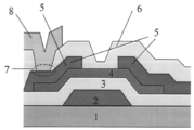
- FIG. 1 is a schematic cross-sectional view for explaining a thin film transistor including a semiconductor layer.
- FIG. 2 is a schematic cross-sectional view for explaining a configuration including an etch stopper layer in the thin film transistor of FIG.
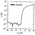
- FIG. 3 is a diagram showing TFT characteristics when IGZO (conventional example) is used for the oxide semiconductor layer.
- FIG. 4 is a graph showing TFT characteristics when In—Zn—Sn—O (comparative example) is used for the oxide semiconductor layer.
- FIG. 5A is a diagram showing TFT characteristics when In—Zn—Hf—O (comparative example) is used for the oxide semiconductor layer.
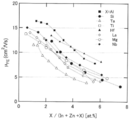
- FIG. 6 is a graph showing the influence of the amount of X on the field effect mobility in In—Zn—X—O.
- FIG. 7 is a graph showing the influence of the amount of In on the field effect mobility in In—Zn—X—O.
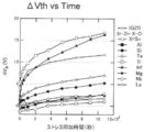
- FIG. 9A is a graph showing the effect of the type of group X element on the time variation of the threshold voltage under positive bias stress in In—Zn—X—O.
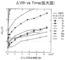
- FIG. 9B is a partially enlarged view of FIG. 9A.
- the inventors of the present invention have studied TFT characteristics and stress resistance (especially positive resistance) when an In—Zn—O oxide (IZO) containing In and Zn and not containing Ga is used for an active layer (semiconductor layer) of a TFT.
- IZO In—Zn—O oxide
- Various studies have been made in order to improve the stress tolerance after bias application.
- X group element selected from the group consisting of Al, Si, Ta, Ti, La, Mg, and Nb
- a TFT including an oxide semiconductor containing an element belonging to the X group (X group element) in IZO has higher mobility than IGZO and is applied with a positive bias. Excellent resistance to stress afterwards.
- a TFT including an oxide semiconductor containing an element other than the X group element for example, Hf, Sn
- Hf, Sn the X group element
- the oxide for a semiconductor layer of the thin film transistor (TFT) according to the present invention is at least one X selected from the group X consisting of In, Zn, Al, Si, Ta, Ti, La, Mg, and Nb. And group elements.
- the oxide of the present invention may be represented by In—Zn—X—O.
- all the metals (In, Zn, and X group elements) constituting the oxide (In—Zn—X—O) of the present invention are included in the In, Zn, and X groups included in the oxide.
- X represented by 100 ⁇ [X] / ([In] + [Zn] + [X]) where the element contents (atomic%) are [In], [Zn], and [X], respectively.
- the amount (atomic%) may be simply abbreviated as X amount.
- [X] is a single amount when it contains one kind of X group element, and is a total amount when it contains two or more kinds of X group elements.
- the In amount (atomic%) represented by 100 ⁇ [In] / ([In] + [Zn] + [X]) may be simply abbreviated as In amount.
- the characteristic part of the present invention is that the above-mentioned group X element is contained in a predetermined amount in In—Zn—O.
- the X group element has an effect of improving stability against positive bias stress (positive bias stress resistance), and elements other than the X group element defined in the present invention (Sn and Compared with the case where Hf) is added, the threshold voltage change ⁇ Vth after applying the positive bias can be significantly reduced (see FIGS. 8 and 9).
- the present invention since the content of the group X element is appropriately controlled, high mobility can be ensured (see FIG. 6).
- the drain current value is not greatly reduced by the addition of the X group element, and the TFT characteristics are good (see FIG. 5).
- the X group element may be added alone or in combination of two or more.
- a preferred X group element type is Al, Ti, or Mg, more preferably Al or Ti, and still more preferably Ti.
- the X group element has an effect of suppressing the generation of oxygen vacancies that cause surplus electrons in the oxide semiconductor. It is considered that oxygen vacancies are reduced by the addition of the group X element, and the stress resistance against stresses such as voltage and light is improved because the oxide has a stable structure.
- the amount of X calculated as described above varies depending on the amount of In, but is preferably about 0.1 to 5 atomic%.
- This amount of X is determined in consideration of the carrier density, the stability of the semiconductor, and the like, and is slightly different depending on the type of the X group element. Strictly speaking, for example, as shown in FIG. 6 to be described later, depending on the type of the X group element, the content that can exhibit the same effect (field effect mobility in FIG. 6) is also different. It is preferable to appropriately control appropriately depending on the type. However, the tendency of the effect due to the addition of the X group element is the same.
- a more preferable X amount varies depending on the type of the X group, but is generally 0.5 to 3 atomic%.
- the amount of In calculated as described above is preferably 15 atomic% or more.
- In has an effect of improving mobility, and the oxide (In—Zn—X—O) of the present invention also shows a tendency that the mobility increases as the In amount increases.
- the In amount is preferably 15 atomic% or more, and more preferably 20 atomic% or more.
- the amount of In becomes too large, the stability of the TFT is lowered, so that it is preferably 70 atomic% or less. More preferably, it is 50 atomic% or less.
- the ratio between the metals is not particularly limited as long as the oxide containing these metals has an amorphous phase and exhibits semiconductor characteristics.
- In—Zn—O itself is also known as a transparent conductive film, and the ratio of each metal capable of forming an amorphous phase (specifically, each molar ratio of InO and ZnO) is described, for example, in Non-Patent Document 1 described above. Has been.
- the oxide is preferably formed by a sputtering method using a sputtering target (hereinafter also referred to as “target”).
- a sputtering target hereinafter also referred to as “target”.
- an oxide can be formed by a chemical film formation method such as a coating method, a thin film excellent in in-plane uniformity of components and film thickness can be easily formed by a sputtering method.
- a sputtering target containing the above-mentioned elements and having the same composition as the desired oxide thereby forming a thin film having a desired component composition without fear of composition deviation.
- an oxide target containing In, Zn, and at least one X group element selected from the X group consisting of Al, Si, Ta, Ti, La, Mg, and Nb is used as a target.
- Such sputtering targets are also included within the scope of the present invention.
- the contents (atomic%) of In, Zn, and X group elements contained in the sputtering target are [In], [Zn], and [X], respectively, 100 ⁇ [X] / ([In ] + [Zn] + [X]) is preferably 0.1 to 5 atomic%.
- the amount of In represented by + [Zn] + [X]) is preferably 15 atomic% or more.
- the group X element is preferably Al, Ti, or Mg, more preferably Al or Ti, and further preferably Ti.
- a film may be formed by using a co-sputtering method (Co-Sputter method) in which two targets having different compositions are discharged at the same time, whereby oxide semiconductor films having different X element contents in the same substrate surface.
- Co-Sputter method a co-sputtering method
- a target containing indium oxide and zinc oxide and a target containing an X group element can be prepared, and an In—Zn—X—O oxide film can be formed by co-sputtering.
- a pure metal target containing only the X group element, an alloy target containing the X group element, an oxide target containing the X group element, or the like can be used.
- the target can be manufactured by, for example, a powder sintering method.
- Sputtering using the target is preferably performed by setting the substrate temperature to room temperature and appropriately controlling the amount of oxygen added.
- a preferable density of the oxide semiconductor layer is 6.0 g / cm 3 or more (described later).
- the gas pressure, input power, and substrate temperature during sputtering film formation it is preferable to appropriately control the gas pressure, input power, and substrate temperature during sputtering film formation.
- the oxide density is also affected by the heat treatment conditions after film formation, it is preferable to appropriately control the heat treatment conditions after film formation.
- Such heat treatment can be controlled, for example, in the thermal history in the TFT manufacturing process. For example, a pre-annealing process (a heat treatment performed immediately after patterning after wet etching of the oxide semiconductor layer) described later is performed. As a result, the film density is improved.
- the gas pressure at the time of film formation is lowered, it is considered that a dense (high density) film can be formed by scattering of sputtered atoms, so the lower the gas pressure at the time of film formation, the better, generally 1-5 mTorr. It is recommended to control within the range. Also, the lower the input power, the better, and it is recommended to set it to approximately 2.0 W / cm 2 or more. It is recommended that the substrate temperature during film formation be controlled within the range of room temperature to 200 ° C. As the heat treatment conditions after film formation, for example, it is recommended that the heat treatment be performed at 250 to 400 ° C. for 10 minutes to 3 hours in an air atmosphere.
- the preferred film thickness of the oxide formed as described above is 30 nm to 200 nm, and more preferably 30 nm to 80 nm.
- the present invention includes a TFT including the oxide as a semiconductor layer of the TFT.
- the TFT is not particularly limited as long as it has at least a gate electrode, a gate insulating film, the above-described oxide semiconductor layer, a source electrode, and a drain electrode on a substrate.
- the density of the oxide semiconductor layer is preferably 6.0 g / cm 3 or more.
- the density of the oxide semiconductor layer is preferably as high as possible, more preferably 6.2 g / cm 3 or more, and still more preferably 6.4 g / cm 3 or more. Note that the density of the oxide semiconductor layer is measured by a method described in Examples described later.
- FIG. 1 illustrates a bottom-gate TFT, but the present invention is not limited thereto, and a top-gate TFT including a gate insulating film and a gate electrode in this order on an oxide semiconductor layer may be used.
- a gate electrode 2 and a gate insulating film 3 are formed on a substrate 1, and an oxide semiconductor layer 4 is formed thereon.
- a source / drain electrode 5 is formed on the oxide semiconductor layer 4, a protective film (insulating film) 6 is formed thereon, and the transparent conductive film 8 is electrically connected to the source / drain electrode 5 through the contact hole 7. It is connected to the.
- the method for forming the gate electrode 2 and the gate insulating film 3 on the substrate 1 is not particularly limited, and a commonly used method can be employed. Further, the types of the gate electrode 2 and the gate insulating film 3 are not particularly limited, and those commonly used can be used.
- the gate electrode 2 Al or Cu metal having a low electrical resistivity, refractory metal such as Mo, Cr, or Ti having high heat resistance, or an alloy thereof can be preferably used.
- the gate insulating film typically include a silicon oxide film, a silicon nitride film, and a silicon oxynitride film. In addition, oxides such as Al 2 O 3 and Y 2 O 3 and those obtained by stacking these can also be used.
- the oxide semiconductor layer 4 is formed.
- the oxide semiconductor layer 4 is preferably formed by a DC sputtering method or an RF sputtering method using a sputtering target having the same composition as the thin film.
- the film may be formed by co-sputtering.
- the oxide semiconductor layer 4 is subjected to wet etching and then patterned. Immediately after the patterning, it is preferable to perform heat treatment (pre-annealing) for improving the film quality of the oxide semiconductor layer 4 so that the on-state current and field-effect mobility of the transistor characteristics are increased and the transistor performance is improved.
- pre-annealing conditions are, for example, temperature: about 250 to 350 ° C., time: about 15 to 120 minutes.
- the source / drain electrodes 5 are formed.
- the type of the source / drain electrode is not particularly limited, and those commonly used can be used.
- a metal or alloy such as Al, Mo, or Cu may be used as in the gate electrode, or pure Ti may be used as in the examples described later.
- a metal thin film can be formed by magnetron sputtering, and then patterned by photolithography, and wet etching can be performed to form an electrode.
- the oxide semiconductor layer 4 is etched and damaged during wet etching, and defects are generated on the surface of the oxide semiconductor layer 4, so that transistor characteristics may be deteriorated.
- a method of forming an etch stopper layer 9 such as SiO 2 on the oxide semiconductor layer 4 to protect the oxide semiconductor layer 4 is generally employed. Yes.
- the etch stopper layer 9 is formed and patterned before forming the source / drain electrodes 5 to protect the channel surface.
- Another method for forming the source / drain electrode 5 is, for example, a method in which a metal thin film is formed by a magnetron sputtering method and then formed by a lift-off method. According to this method, it is also possible to process the electrode without performing wet etching. In the examples described later, this method is employed. After forming a metal thin film, patterning was performed using a lift-off method.
- a protective film (insulating film) 6 is formed over the oxide semiconductor layer 4 by a CVD (Chemical Vapor Deposition) method.
- the surface of the oxide semiconductor film easily becomes conductive due to plasma damage caused by CVD (probably because oxygen vacancies generated on the surface of the oxide semiconductor serve as electron donors), thus avoiding the above problem. Therefore, in the embodiment described below, it was N 2 O plasma irradiation before the formation of the protective film.
- the conditions described in the following document were adopted as the irradiation conditions of N 2 O plasma. J. et al. Park et al., Appl. Phys. Lett. , 1993, 053505 (2008).
- the transparent conductive film 8 is electrically connected to the drain electrode 5 through the contact hole 7.
- the types of the transparent conductive film and the drain electrode are not particularly limited, and commonly used ones can be used.
- As the drain electrode for example, those exemplified for the source / drain electrodes described above can be used.
- Example 1 Based on the method described above, the thin film transistor (TFT) shown in FIG. 1 was fabricated and evaluated for each characteristic.
- a glass substrate (Corning EAGLE 2000, diameter 100 mm ⁇ thickness 0.7 mm) on the Mo film as the gate electrode 100 nm, and the gate insulating film were sequentially formed SiO 2 a (200 nm).
- the gate electrode was formed by DC sputtering using a pure Mo sputtering target.
- the sputtering conditions were a film formation power density of 3.8 W / cm 2 at room temperature, a gas pressure of 2 mTorr, and an Ar gas flow rate of 20 sccm.
- the gate insulating film was formed by plasma CVD using a carrier gas: a mixed gas of SiH 4 and N 2 O, a deposition power of 1.27 W / cm 3 , and a deposition temperature of 320 ° C.
- the gas pressure during film formation was 133 Pa.
- oxide thin films having various compositions described in Table 1 to be described later were formed by a sputtering method using a sputtering target (described later).
- a sputtering target As an oxide thin film, in addition to In—Zn—X—O (invention example) containing an X group element in In—Zn—O, for comparison, IGZO containing Ga as an element other than the X group element (for example) Conventional examples), In—Zn—Sn—O containing Sn (conventional example), and In—Zn—Hf—O containing Hf (comparative example) were also formed.
- a sputtering target having an In: Ga: Zn ratio (atomic% ratio) of 1: 1: 1 was used, and a film was formed using a DC sputtering method.
- a sputtering target having an In: Ga: Zn ratio (atomic% ratio) of 1: 1: 1 was used, and a film was formed using a DC sputtering method.
- In—Zn—X—O Al, Si, Ta, Ti, La, Mg, Nb
- In—Zn—Hf—O, and In—Zn—Sn—O was formed using a Co-Sputter method in which three sputtering targets having different compositions were discharged simultaneously.
- three types of sputtering targets were used: indium oxide (In 2 O 3 ), zinc oxide (ZnO), and an oxide target of an X group element.
- Each content of the metal element in the oxide thin film thus obtained was analyzed by an XPS (X-ray Photoelectron Spectroscopy) method.
- Pre-annealing was performed to improve the film quality. Pre-annealing was performed at 350 ° C. for 1 hour in an air atmosphere.
- pure Ti was used to form source / drain electrodes by a lift-off method. Specifically, after patterning using a photoresist, a Ti thin film was formed by DC sputtering (film thickness was 100 nm). The conditions for forming the Ti thin film for the source / drain electrodes are the same as those for the gate electrode described above. Subsequently, unnecessary photoresist was removed by applying an ultrasonic cleaner in an acetone solution, and lift-off was performed. The channel length of the TFT was 10 ⁇ m and the channel width was 200 ⁇ m.
- a protective film for protecting the oxide semiconductor layer was formed.
- a laminated film (total film thickness 150 nm) of SiO 2 (film thickness 200 nm) and SiN (film thickness 150 nm) was used.
- the above-mentioned SiO 2 and SiN were formed using “PD-220NL” manufactured by Samco and using the plasma CVD method.
- SiO 2 and SiN films were sequentially formed.
- a mixed gas of N 2 O and SiH 4 was used for forming the SiO 2 film, and a mixed gas of SiH 4 , N 2 , and NH 3 was used for forming the SiN film.
- the film formation power was 100 W and the film formation temperature was 150 ° C.
- ITO film film thickness: 80 nm
- a carrier gas a mixed gas of argon and oxygen gas
- film formation power 200 W
- gas pressure 5 mTorr
- transistor characteristics drain current-gate voltage characteristics, Id-Vg characteristics
- threshold voltage threshold voltage
- S value S value
- Field effect mobility (5) Stress tolerance after applying positive bias stress were examined.
- transistor characteristics were measured by using a semiconductor parameter analyzer “4156C” manufactured by Agilent Technology. Detailed measurement conditions are as follows. Source voltage: 0V Drain voltage: 10V Gate voltage: -30 to 30V (measurement interval: 0.25V) Substrate temperature: room temperature
- Threshold voltage The threshold voltage is roughly a value of a gate voltage when the transistor shifts from an off state (a state where the drain current is low) to an on state (a state where the drain current is high).
- the threshold voltage is defined as a voltage when the drain current is in the vicinity of 1 nA between the on-current and the off-current.
- S value is the minimum value of the gate voltage required to increase the drain current when rising from the off state to the on state in the Id-Vg characteristic, and the lower the S value, the more the drain current The increase becomes steep, indicating that the device characteristics are good.
- the field effect mobility ⁇ FE was derived from the TFT characteristics in a saturation region where V d > V g ⁇ V th .
- V g and V th are the gate voltage and threshold voltage
- I d is the drain current
- L and W are the channel length and channel width of the TFT element
- C i is the capacitance of the gate insulating film
- ⁇ FE was defined as field effect mobility.
- the field effect mobility ⁇ FE is derived from the following equation. In this example, the field effect mobility ⁇ FE was derived from the drain current-gate voltage characteristics (I d -V g characteristics) in the vicinity of the gate voltage satisfying the saturation region.
- FIG. 3 shows the Id-Vg characteristics of a TFT using a conventional IGZO (In—Ga—Zn—O) as a semiconductor layer, and the composition of IGZO is In atomic ratio (molar ratio).
- Ga: Zn 1: 1: 1.
- FIG. 4 shows Id—Vg characteristics in a TFT using In—Zn—Sn—O as a semiconductor layer.
- Zn: Sn is an atomic ratio (molar ratio)
- In: Zn: Sn 30: 60:10 (Note that the molar ratio of In: Zn is 1: 2).
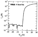
- FIG. 5A (a) to (d) show In—Ga—X—O with Si, Al, Ta, and Ti added as an X group element
- FIG. 5A (e) shows Hf as an element other than the X group element.
- Each of the added In—Ga—Hf—O shows the Id—Vg characteristics of the TFTs used in the semiconductor layer, and in each case, the In amount is 30 atomic%, and in (a), the Si amount is 3.1. Atomic%, (b) Al content is 1.6 atomic%, (c) Ta content is 1.4 atomic%, (d) Ti content is 2.4 atomic%, (e) Hf content is 3 0.0 atomic percent.
- the molar ratio of In: Zn is about 30:60 to 70 for all.
- 5B (a) to 5 (c) show Id-Vg characteristics in a TFT using a semiconductor layer of In—Ga—X—O containing La, Mg, and Nb as X group elements.
- the In content is 30 atomic%
- the La content is 2 atomic% in (a)
- the Mg content is 2 atomic% in (b)
- the Nb content is 1 atomic% in (c).
- the molar ratio of In: Zn is about 30:60 to 70 for all.
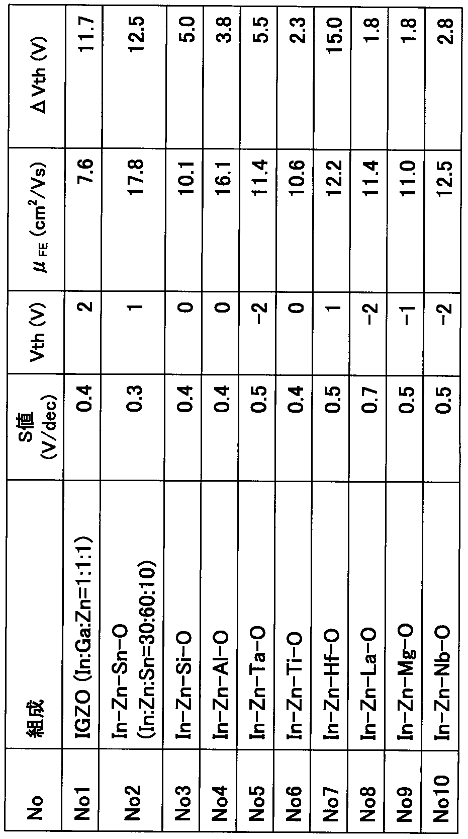
- Table 1 summarizes the characteristic results of TFTs using the above oxides as semiconductor layers.
- the I d -V g characteristic of the conventional IGZO (No. 1 in Table 1) will be described with reference to FIG.
- V g near 0V increases from the negative side to the positive side.
- all examples had very high mobility exceeding the value of conventional IGZO (7.6 cm 2 / Vs).
- ⁇ Hf
- ⁇ Mg
- ⁇ La
- FIG. 7 shows a relationship between the amount of In and the threshold voltage V th with ⁇ .
- the threshold voltage V th hardly varies with the addition of the In amount, but the field effect mobility ⁇ FE has a high In amount dependency, and the electric field increases as the In amount increases. It can be seen that the effect mobility is improved. Specifically, the field effect mobility tended to increase rapidly from the vicinity of 10 atomic% of the In amount, and the mobility increased gradually when the In amount was about 20 atomic%.
- FIG. 7 shows the results when Al is added as an X group element.
- Al is added as an X group element.
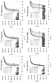
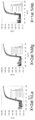
- the graph shows changes over time in TFT characteristics when a positive bias is applied for 0 to 3 hours (10800 seconds) at a substrate temperature of 60 ° C.
- these figures show the results when the substrate temperature is 25 ° C. (room temperature) (shown as “as depo” in FIG. 8), which has a corresponding X group element. The results are the same as those shown in FIGS.
- FIG. 8A reference is first made to a graph of Hf and Sn not defined by the present invention.
- the threshold voltage V th is shifted in the positive direction due to the increase of the substrate temperature. It can be seen that the threshold voltage shifts further to the positive side as the stress application time becomes longer (see ⁇ in the figure, the stress application time becomes longer from 0 sec to 10800 sec in the direction of the arrow). This is presumably because an acceptor-like defect occurred at the interface between the gate insulating film and the semiconductor layer as a result of continuing to apply a positive bias to the TFT, and electrons were trapped at the interface.
- the threshold voltage V due to heating at a substrate temperature of 25 ° C. ⁇ 60 ° C. It can be seen that there is no significant change in th , and that even when positive bias stress is continuously applied, the change in V th is smaller than when Sn or Hf is used.
- FIGS. 9A and 9B are shown in FIGS. 9A and 9B.
- FIG. 9B is a partially enlarged view of FIG. 9A.
- the threshold voltage change amount [Delta] V th of the stress application time is obtained by calculating as the difference between the threshold voltage at the stress time, the threshold voltage before stress application.
- the result of IGZO (conventional example) is also shown for reference.
- the threshold voltage V th is shifted in the positive direction when a positive bias is applied, regardless of the type of the X group element. This is presumably because the number of electrons trapped at the interface between the semiconductor layer and the gate insulating film increases by applying a positive bias.
- IGZO in the conventional example is 11.7 V
- ⁇ V th is further increased. It became high and was 16.8V.
- ⁇ V th of the example ( ⁇ ) containing Hf not specified in the present invention was also high, 16.3V. That is, these examples were found to be extremely inferior to positive bias stress tolerance.
- the element added with the X group element defined in the present invention shows good characteristics with the S value and mobility after applying a positive bias stress almost unchanged from those before applying stress. Yes.
- Example 2 In this example, the relationship between the density of the oxide semiconductor film and the TFT characteristics was examined for oxides having the compositions shown in Table 2. Specifically, the density of the oxide film (film thickness: 100 nm) was measured by the following method, and a TFT was produced in the same manner as in Example 1 described above, and the electrolytic effect mobility was measured.
- Table 2 No. 1 in Table 2
- the composition of the oxides 1 and 2 (In—Zn—Sn—O) is shown in No. 1 of Table 1 above. No. 2 in Table 2;
- the composition of the oxides 3 and 4 In—Zn—Al—O) is shown in No. 1 in Table 1 above. No.
- the density of the oxide was measured using XRR (X-ray reflectivity method). Detailed measurement conditions are as follows.
- Table 2 shows the results of Al and Ti as the X group element, but the relationship between the density of the oxide film and the field effect mobility described above is similarly seen when other X group elements are used. It was. From the above results, it can be seen that when the density of the oxide semiconductor layer is 6.0 g / cm 3 or more, a TFT having sufficiently high practical mobility can be obtained.
Landscapes
- Chemical & Material Sciences (AREA)
- Engineering & Computer Science (AREA)
- Organic Chemistry (AREA)
- Materials Engineering (AREA)
- Mechanical Engineering (AREA)
- Metallurgy (AREA)
- Chemical Kinetics & Catalysis (AREA)
- Physics & Mathematics (AREA)
- Geometry (AREA)
- Microelectronics & Electronic Packaging (AREA)
- Thin Film Transistor (AREA)
- Liquid Crystal (AREA)
- Inorganic Compounds Of Heavy Metals (AREA)
- Electroluminescent Light Sources (AREA)
- Physical Vapour Deposition (AREA)
Abstract
Description
J. Parkら、Appl. Phys. Lett., 1993,053505(2008)
前述した方法に基づき、図1に示す薄膜トランジスタ(TFT)を作製し、各特性を評価した。
基板温度:室温
ガス圧:5mTorr
酸素分圧:O2/(Ar+O2)=2%
成膜パワー密度:2.55W/cm2
膜厚:50nm
トランジスタ特性の測定はAgilent Technology社製「4156C」の半導体パラメータアナライザーを使用した。詳細な測定条件は以下のとおりである。
ソース電圧 :0V
ドレイン電圧:10V
ゲート電圧 :-30~30V(測定間隔:0.25V)
基板温度:室温
しきい値電圧とは、おおまかにいえば、トランジスタがオフ状態(ドレイン電流の低い状態)からオン状態(ドレイン電流の高い状態)に移行する際のゲート電圧の値である。本実施例では、ドレイン電流が、オン電流とオフ電流の間の1nA付近であるときの電圧をしきい値電圧と定義した。
S値は、Id-Vg特性においてオフ状態からオン状態に立ち上がる際のドレイン電流を一桁増加させるのに必要なゲート電圧の最小値であり、S値が低いほどドレイン電流の増加が急峻となり、デバイス特性が良好であることを示す。
電界効果移動度μFEは、TFT特性からVd>Vg-Vthである飽和領域にて導出した。飽和領域ではVg、Vthをそれぞれゲート電圧、しきい値電圧、Idをドレイン電流、L、WをそれぞれTFT素子のチャネル長、チャネル幅、Ciをゲート絶縁膜の静電容量、μFEを電界効果移動度とした。電界効果移動度μFEは下式から導出される。本実施例では、飽和領域を満たすゲート電圧付近におけるドレイン電流-ゲート電圧特性(Id-Vg特性)から電界効果移動度μFEを導出した。

本実施例では、実際のパネル駆動時の環境(ストレス)を模擬して、ゲート電極に正バイアスをかけながらストレス印加試験を行った。ストレス印加条件は以下のとおりである。特に有機ELディスプレイの場合、正バイアスストレスによりしきい値電圧が変動して電流値が低下するため、しきい値電圧の変化が小さいほどよい。
ソース電圧:0V
ドレイン電圧:0.1V
ゲート電圧:20V
基板温度:60℃
ストレス印加時間:3時間
本実施例では、表2に記載の組成を有する酸化物について、酸化物半導体膜の密度とTFT特性の関係を調べた。詳細には、以下の方法で酸化物膜(膜厚100nm)の密度を測定すると共に、前述した実施例1と同様にしてTFTを作製し、電解効果移動度を測定した。表2において、表2のNo.1および2の酸化物の組成(In-Zn-Sn-O)は、前述した表1のNo.2と同じであり;表2のNo.3および4の酸化物の組成(In-Zn-Al-O)は、前述した表1のNo.4と同じであり;表2のNo.5および6の酸化物の組成(In-Zn-Ti-O)は、前述した表1のNo.6と同じであり;表2のNo.7の酸化物の組成(In-Zn-La-O)は、前述した表1のNo.8と同じであり;表2のNo.8の酸化物の組成(In-Zn-Mg-O)は、前述した表1のNo.9と同じであり;表2のNo.9の酸化物の組成(In-Zn-Nb-O)は、前述した表1のNo.10と同じである。
酸化物の密度は、XRR(X線反射率法)を用いて測定した。詳細な測定条件は以下のとおりである。
・ターゲット:Cu(線源:Kα線)
・ターゲット出力:45kV-200mA
・測定試料の作製
ガラス基板上に各組成の酸化物を下記スパッタリング条件で成膜した(膜厚100nm)後、前述した実施例1のTFT製造過程におけるプレアニール処理を模擬して、当該プレアニール処理と同じ熱処理を施したものを使用
スパッタガス圧:1mTorrまたは5mTorr
酸素分圧:O2/(Ar+O2)=2%
成膜パワー密度:2.55W/cm2
熱処理:大気雰囲気にて350℃で1時間

2 ゲート電極
3 ゲート絶縁膜
4 酸化物半導体層
5 ソース・ドレイン電極
6 保護膜(絶縁膜)
7 コンタクトホール
8 透明導電膜
9 エッチストッパー層
Claims (13)
- 薄膜トランジスタの半導体層に用いられる酸化物であって、
前記酸化物は、Inと;Znと;Al、Si、Ta、Ti、La、Mg、およびNbよりなる群から選択される少なくとも一種の元素(X群元素)と、を含むことを特徴とする薄膜トランジスタの半導体層用酸化物。 - 半導体層用酸化物に含まれるIn、Zn、X群元素の含有量(原子%)をそれぞれ、[In]、[Zn]、[X]としたとき、100×[X]/([In]+[Zn]+[X])で表されるX量は0.1~5原子%である請求項1に記載の酸化物。
- 半導体層用酸化物に含まれるIn、Zn、X群元素の含有量(原子%)をそれぞれ、[In]、[Zn]、[X]としたとき、100×[In]/([In]+[Zn]+[X])で表されるIn量は15原子%以上である請求項1に記載の酸化物。
- 半導体層用酸化物に含まれるIn、Zn、X群元素の含有量(原子%)をそれぞれ、[In]、[Zn]、[X]としたとき、100×[In]/([In]+[Zn]+[X])で表されるIn量は15原子%以上である請求項2に記載の酸化物。
- 前記X群元素はAl、Ti、またはMgである請求項1に記載の酸化物。
- 請求項1~5のいずれかに記載の酸化物を薄膜トランジスタの半導体層として備えた薄膜トランジスタ。
- 前記半導体層の密度は6.0g/cm3以上である請求項6に記載の薄膜トランジスタ。
- 請求項6に記載の薄膜トランジスタを備えた表示装置。
- 請求項6に記載の薄膜トランジスタを備えた有機EL表示装置。
- 請求項1~5のいずれかに記載の酸化物を成膜するためのスパッタリングターゲットであって、
Inと;Znと;Al、Si、Ta、Ti、La、Mg、およびNbよりなる群から選択される少なくとも一種の元素(X群元素)と、を含むことを特徴とするスパッタリングターゲット。 - スパッタリングターゲット中に含まれるIn、Zn、X群元素の含有量(原子%)をそれぞれ、[In]、[Zn]、[X]としたとき、100×[X]/([In]+[Zn]+[X])で表されるX量は0.1~5原子%である請求項10に記載のスパッタリングターゲット。
- スパッタリングターゲット中に含まれるIn、Zn、X群元素の含有量(原子%)をそれぞれ、[In]、[Zn]、[X]としたとき、100×[In]/([In]+[Zn]+[X])で表されるIn量は15原子%以上である請求項10に記載のスパッタリングターゲット。
- 前記X群元素はAl、Ti、またはMgである請求項10に記載のスパッタリングターゲット。
Priority Applications (3)
| Application Number | Priority Date | Filing Date | Title |
|---|---|---|---|
| US13/994,467 US20130270109A1 (en) | 2010-12-28 | 2011-12-28 | Oxide for semiconductor layer of thin-film transistor, sputtering target, and thin-film transistor |
| CN2011800618352A CN103270602A (zh) | 2010-12-28 | 2011-12-28 | 薄膜晶体管的半导体层用氧化物及溅射靶材,以及薄膜晶体管 |
| KR1020137019491A KR20130097809A (ko) | 2010-12-28 | 2011-12-28 | 박막 트랜지스터의 반도체층용 산화물 및 스퍼터링 타깃, 및 박막 트랜지스터 |
Applications Claiming Priority (2)
| Application Number | Priority Date | Filing Date | Title |
|---|---|---|---|
| JP2010292929 | 2010-12-28 | ||
| JP2010-292929 | 2010-12-28 |
Publications (1)
| Publication Number | Publication Date |
|---|---|
| WO2012091126A1 true WO2012091126A1 (ja) | 2012-07-05 |
Family
ID=46383213
Family Applications (1)
| Application Number | Title | Priority Date | Filing Date |
|---|---|---|---|
| PCT/JP2011/080483 Ceased WO2012091126A1 (ja) | 2010-12-28 | 2011-12-28 | 薄膜トランジスタの半導体層用酸化物およびスパッタリングターゲット、並びに薄膜トランジスタ |
Country Status (6)
| Country | Link |
|---|---|
| US (1) | US20130270109A1 (ja) |
| JP (1) | JP2012151469A (ja) |
| KR (1) | KR20130097809A (ja) |
| CN (1) | CN103270602A (ja) |
| TW (1) | TWI507554B (ja) |
| WO (1) | WO2012091126A1 (ja) |
Cited By (2)
| Publication number | Priority date | Publication date | Assignee | Title |
|---|---|---|---|---|
| JP2020532856A (ja) * | 2017-08-29 | 2020-11-12 | マイクロン テクノロジー,インク. | 高バンド・ギャップ材料を含むストリング・ドライバを備えたデバイス及びシステム、並びに形成の方法 |
| WO2023145497A1 (ja) * | 2022-01-31 | 2023-08-03 | 三井金属鉱業株式会社 | 電界効果トランジスタ及びその製造方法並びに電界効果トランジスタ製造用スパッタリングターゲット材 |
Families Citing this family (29)
| Publication number | Priority date | Publication date | Assignee | Title |
|---|---|---|---|---|
| JP2012124446A (ja) | 2010-04-07 | 2012-06-28 | Kobe Steel Ltd | 薄膜トランジスタの半導体層用酸化物およびスパッタリングターゲット、並びに薄膜トランジスタ |
| JP2012033854A (ja) | 2010-04-20 | 2012-02-16 | Kobe Steel Ltd | 薄膜トランジスタの半導体層用酸化物およびスパッタリングターゲット、並びに薄膜トランジスタ |
| JP5718072B2 (ja) | 2010-07-30 | 2015-05-13 | 三星ディスプレイ株式會社Samsung Display Co.,Ltd. | 薄膜トランジスタの半導体層用酸化物およびスパッタリングターゲット、並びに薄膜トランジスタ |
| JP5651095B2 (ja) | 2010-11-16 | 2015-01-07 | 株式会社コベルコ科研 | 酸化物焼結体およびスパッタリングターゲット |
| JP5811877B2 (ja) * | 2012-02-09 | 2015-11-11 | 住友電気工業株式会社 | 導電性酸化物およびその製造方法 |
| WO2013168748A1 (ja) | 2012-05-09 | 2013-11-14 | 株式会社神戸製鋼所 | 薄膜トランジスタおよび表示装置 |
| JP6068232B2 (ja) | 2012-05-30 | 2017-01-25 | 株式会社神戸製鋼所 | 薄膜トランジスタの半導体層用酸化物、薄膜トランジスタ、表示装置およびスパッタリングターゲット |
| CN104335353B (zh) | 2012-06-06 | 2017-04-05 | 株式会社神户制钢所 | 薄膜晶体管 |
| JP6002088B2 (ja) | 2012-06-06 | 2016-10-05 | 株式会社神戸製鋼所 | 薄膜トランジスタ |
| JP2014225626A (ja) | 2012-08-31 | 2014-12-04 | 株式会社神戸製鋼所 | 薄膜トランジスタおよび表示装置 |
| JP6134230B2 (ja) * | 2012-08-31 | 2017-05-24 | 株式会社神戸製鋼所 | 薄膜トランジスタおよび表示装置 |
| JP6006055B2 (ja) * | 2012-09-07 | 2016-10-12 | 出光興産株式会社 | スパッタリングターゲット |
| JP5947697B2 (ja) * | 2012-10-19 | 2016-07-06 | 出光興産株式会社 | スパッタリングターゲット |
| JP6188712B2 (ja) * | 2012-11-08 | 2017-08-30 | 出光興産株式会社 | スパッタリングターゲット |
| JP6025595B2 (ja) * | 2013-02-15 | 2016-11-16 | 三菱電機株式会社 | 薄膜トランジスタの製造方法 |
| US9312392B2 (en) * | 2013-05-16 | 2016-04-12 | Semiconductor Energy Laboratory Co., Ltd. | Semiconductor device |
| JP2015195327A (ja) * | 2013-06-05 | 2015-11-05 | 株式会社半導体エネルギー研究所 | 半導体装置 |
| JP2015030858A (ja) * | 2013-07-31 | 2015-02-16 | 株式会社アルバック | スパッタリングターゲットの製造方法 |
| KR102120075B1 (ko) * | 2013-12-30 | 2020-06-08 | 엘지디스플레이 주식회사 | 유기발광표시장치 |
| KR101630028B1 (ko) * | 2014-03-03 | 2016-06-13 | 부산대학교 산학협력단 | Pdms 패시베이션층을 적용한 알루미늄-인듐 아연 산화물 반도체 박막트랜지스터의 제조방법 및 이에 의해 제조된 알루미늄-인듐 아연 산화물 반도체 박막트랜지스터 |
| KR20150105527A (ko) | 2014-03-06 | 2015-09-17 | 삼성디스플레이 주식회사 | 산화물 스퍼터링 타겟 및 이를 이용한 박막 트랜지스터 |
| CN108352410B (zh) * | 2015-11-25 | 2021-06-29 | 株式会社爱发科 | 薄膜晶体管、氧化物半导体膜以及溅射靶材 |
| KR102448587B1 (ko) * | 2016-03-22 | 2022-09-28 | 가부시키가이샤 한도오따이 에네루기 켄큐쇼 | 반도체 장치, 및 상기 반도체 장치를 포함하는 표시 장치 |
| JP6800405B2 (ja) * | 2016-07-14 | 2020-12-16 | 東ソー株式会社 | 酸化物焼結体、その製造方法及びスパッタリングターゲット |
| US20230307549A1 (en) * | 2020-08-05 | 2023-09-28 | Mitsui Mining & Smelting Co., Ltd. | Sputtering target material and oxide semiconductor |
| CN113735564A (zh) * | 2021-08-11 | 2021-12-03 | 芜湖映日科技股份有限公司 | 一种Nb掺杂IZO靶胚及其制备方法 |
| WO2023145498A1 (ja) * | 2022-01-31 | 2023-08-03 | 三井金属鉱業株式会社 | スパッタリングターゲット材及び酸化物半導体の製造方法 |
| WO2023145499A1 (ja) * | 2022-01-31 | 2023-08-03 | 三井金属鉱業株式会社 | スパッタリングターゲット |
| US20250220976A1 (en) * | 2022-04-15 | 2025-07-03 | Kabushiki Kaisha Kobe Seiko Sho (Kobe Steel, Ltd.) | Oxide semiconductor film, thin film transistor, sputtering target, and oxide sintered body |
Citations (3)
| Publication number | Priority date | Publication date | Assignee | Title |
|---|---|---|---|---|
| JP2010030824A (ja) * | 2008-07-28 | 2010-02-12 | Idemitsu Kosan Co Ltd | 金属相含有酸化インジウム焼結体及びその製造方法 |
| JP2010222214A (ja) * | 2009-03-25 | 2010-10-07 | Idemitsu Kosan Co Ltd | 金属酸化物薄膜及びその製造方法 |
| JP2010272663A (ja) * | 2009-05-21 | 2010-12-02 | Sony Corp | 薄膜トランジスタ、表示装置、および電子機器 |
Family Cites Families (6)
| Publication number | Priority date | Publication date | Assignee | Title |
|---|---|---|---|---|
| KR101514766B1 (ko) * | 2001-07-17 | 2015-05-12 | 이데미쓰 고산 가부시키가이샤 | 스퍼터링 타겟 및 투명 도전막 |
| JP4221940B2 (ja) * | 2002-03-13 | 2009-02-12 | ソニー株式会社 | 固体撮像素子及び固体撮像装置並びに撮像システム |
| CN101681925B (zh) * | 2007-06-19 | 2011-11-30 | 三星电子株式会社 | 氧化物半导体及包含该氧化物半导体的薄膜晶体管 |
| US8461583B2 (en) * | 2007-12-25 | 2013-06-11 | Idemitsu Kosan Co., Ltd. | Oxide semiconductor field effect transistor and method for manufacturing the same |
| JP5096250B2 (ja) * | 2008-07-18 | 2012-12-12 | 出光興産株式会社 | 酸化物焼結体の製造方法、酸化物焼結体、スパッタリングタ−ゲット、酸化物薄膜、薄膜トランジスタの製造方法及び半導体装置 |
| JP5081959B2 (ja) * | 2010-08-31 | 2012-11-28 | Jx日鉱日石金属株式会社 | 酸化物焼結体及び酸化物半導体薄膜 |
-
2011
- 2011-12-28 TW TW100149224A patent/TWI507554B/zh not_active IP Right Cessation
- 2011-12-28 JP JP2011287287A patent/JP2012151469A/ja active Pending
- 2011-12-28 KR KR1020137019491A patent/KR20130097809A/ko not_active Ceased
- 2011-12-28 US US13/994,467 patent/US20130270109A1/en not_active Abandoned
- 2011-12-28 WO PCT/JP2011/080483 patent/WO2012091126A1/ja not_active Ceased
- 2011-12-28 CN CN2011800618352A patent/CN103270602A/zh active Pending
Patent Citations (3)
| Publication number | Priority date | Publication date | Assignee | Title |
|---|---|---|---|---|
| JP2010030824A (ja) * | 2008-07-28 | 2010-02-12 | Idemitsu Kosan Co Ltd | 金属相含有酸化インジウム焼結体及びその製造方法 |
| JP2010222214A (ja) * | 2009-03-25 | 2010-10-07 | Idemitsu Kosan Co Ltd | 金属酸化物薄膜及びその製造方法 |
| JP2010272663A (ja) * | 2009-05-21 | 2010-12-02 | Sony Corp | 薄膜トランジスタ、表示装置、および電子機器 |
Cited By (5)
| Publication number | Priority date | Publication date | Assignee | Title |
|---|---|---|---|---|
| JP2020532856A (ja) * | 2017-08-29 | 2020-11-12 | マイクロン テクノロジー,インク. | 高バンド・ギャップ材料を含むストリング・ドライバを備えたデバイス及びシステム、並びに形成の方法 |
| JP7097952B2 (ja) | 2017-08-29 | 2022-07-08 | マイクロン テクノロジー,インク. | 高バンド・ギャップ材料を含むストリング・ドライバを備えたデバイス及びシステム、並びに形成の方法 |
| WO2023145497A1 (ja) * | 2022-01-31 | 2023-08-03 | 三井金属鉱業株式会社 | 電界効果トランジスタ及びその製造方法並びに電界効果トランジスタ製造用スパッタリングターゲット材 |
| JP7364824B1 (ja) * | 2022-01-31 | 2023-10-18 | 三井金属鉱業株式会社 | 電界効果トランジスタ及びその製造方法並びに電界効果トランジスタ製造用スパッタリングターゲット材 |
| TWI846271B (zh) * | 2022-01-31 | 2024-06-21 | 日商三井金屬鑛業股份有限公司 | 場效電晶體及其製造方法、以及場效電晶體製造用濺鍍靶材 |
Also Published As
| Publication number | Publication date |
|---|---|
| TWI507554B (zh) | 2015-11-11 |
| TW201243070A (en) | 2012-11-01 |
| US20130270109A1 (en) | 2013-10-17 |
| JP2012151469A (ja) | 2012-08-09 |
| KR20130097809A (ko) | 2013-09-03 |
| CN103270602A (zh) | 2013-08-28 |
Similar Documents
| Publication | Publication Date | Title |
|---|---|---|
| JP5723262B2 (ja) | 薄膜トランジスタおよびスパッタリングターゲット | |
| TWI507554B (zh) | An oxide and a sputtering target for a semiconductor layer of a thin film transistor, and a thin film transistor | |
| JP6043244B2 (ja) | 薄膜トランジスタ | |
| JP5718072B2 (ja) | 薄膜トランジスタの半導体層用酸化物およびスパッタリングターゲット、並びに薄膜トランジスタ | |
| KR101459983B1 (ko) | 박막 트랜지스터의 반도체층용 산화물 및 스퍼터링 타깃 및 박막 트랜지스터 | |
| US10468535B2 (en) | Oxide for semiconductor layer of thin film transistor, sputtering target, and thin film transistor | |
| KR101407402B1 (ko) | 박막 트랜지스터의 반도체층용 산화물 및 스퍼터링 타깃, 및 박막 트랜지스터 | |
| JP6018551B2 (ja) | 薄膜トランジスタ | |
| JP5977569B2 (ja) | 薄膜トランジスタ構造、ならびにその構造を備えた薄膜トランジスタおよび表示装置 | |
| JP6294428B2 (ja) | 薄膜トランジスタの半導体層用酸化物の製造方法、および薄膜トランジスタの特性を向上する方法 | |
| KR102124867B1 (ko) | 박막 트랜지스터의 반도체층용 산화물 및 스퍼터링 타깃 및 박막 트랜지스터 | |
| CN104335354B (zh) | 薄膜晶体管的半导体层用氧化物、薄膜晶体管、显示装置及溅射靶 | |
| WO2013168748A1 (ja) | 薄膜トランジスタおよび表示装置 | |
| JP5645737B2 (ja) | 薄膜トランジスタ構造および表示装置 | |
| JP2013207100A (ja) | 薄膜トランジスタ | |
| JP2016026389A (ja) | 薄膜トランジスタの半導体層用酸化物およびスパッタリングターゲット、並びに薄膜トランジスタ |
Legal Events
| Date | Code | Title | Description |
|---|---|---|---|
| 121 | Ep: the epo has been informed by wipo that ep was designated in this application |
Ref document number: 11853507 Country of ref document: EP Kind code of ref document: A1 |
|
| WWE | Wipo information: entry into national phase |
Ref document number: 13994467 Country of ref document: US |
|
| NENP | Non-entry into the national phase |
Ref country code: DE |
|
| ENP | Entry into the national phase |
Ref document number: 20137019491 Country of ref document: KR Kind code of ref document: A |
|
| 122 | Ep: pct application non-entry in european phase |
Ref document number: 11853507 Country of ref document: EP Kind code of ref document: A1 |