WO2012090366A1 - ワークの研磨方法及び研磨装置 - Google Patents
ワークの研磨方法及び研磨装置 Download PDFInfo
- Publication number
- WO2012090366A1 WO2012090366A1 PCT/JP2011/005856 JP2011005856W WO2012090366A1 WO 2012090366 A1 WO2012090366 A1 WO 2012090366A1 JP 2011005856 W JP2011005856 W JP 2011005856W WO 2012090366 A1 WO2012090366 A1 WO 2012090366A1
- Authority
- WO
- WIPO (PCT)
- Prior art keywords
- polishing
- carrier plate
- temperature
- workpiece
- wafer
- Prior art date
- Legal status (The legal status is an assumption and is not a legal conclusion. Google has not performed a legal analysis and makes no representation as to the accuracy of the status listed.)
- Ceased
Links
Images





Classifications
-
- H—ELECTRICITY
- H10—SEMICONDUCTOR DEVICES; ELECTRIC SOLID-STATE DEVICES NOT OTHERWISE PROVIDED FOR
- H10P—GENERIC PROCESSES OR APPARATUS FOR THE MANUFACTURE OR TREATMENT OF DEVICES COVERED BY CLASS H10
- H10P52/00—Grinding, lapping or polishing of wafers, substrates or parts of devices
-
- B—PERFORMING OPERATIONS; TRANSPORTING
- B24—GRINDING; POLISHING
- B24B—MACHINES, DEVICES, OR PROCESSES FOR GRINDING OR POLISHING; DRESSING OR CONDITIONING OF ABRADING SURFACES; FEEDING OF GRINDING, POLISHING, OR LAPPING AGENTS
- B24B37/00—Lapping machines or devices; Accessories
- B24B37/005—Control means for lapping machines or devices
-
- B—PERFORMING OPERATIONS; TRANSPORTING
- B24—GRINDING; POLISHING
- B24B—MACHINES, DEVICES, OR PROCESSES FOR GRINDING OR POLISHING; DRESSING OR CONDITIONING OF ABRADING SURFACES; FEEDING OF GRINDING, POLISHING, OR LAPPING AGENTS
- B24B37/00—Lapping machines or devices; Accessories
-
- B—PERFORMING OPERATIONS; TRANSPORTING
- B24—GRINDING; POLISHING
- B24B—MACHINES, DEVICES, OR PROCESSES FOR GRINDING OR POLISHING; DRESSING OR CONDITIONING OF ABRADING SURFACES; FEEDING OF GRINDING, POLISHING, OR LAPPING AGENTS
- B24B37/00—Lapping machines or devices; Accessories
- B24B37/005—Control means for lapping machines or devices
- B24B37/015—Temperature control
-
- B—PERFORMING OPERATIONS; TRANSPORTING
- B24—GRINDING; POLISHING
- B24B—MACHINES, DEVICES, OR PROCESSES FOR GRINDING OR POLISHING; DRESSING OR CONDITIONING OF ABRADING SURFACES; FEEDING OF GRINDING, POLISHING, OR LAPPING AGENTS
- B24B37/00—Lapping machines or devices; Accessories
- B24B37/04—Lapping machines or devices; Accessories designed for working plane surfaces
-
- B—PERFORMING OPERATIONS; TRANSPORTING
- B24—GRINDING; POLISHING
- B24B—MACHINES, DEVICES, OR PROCESSES FOR GRINDING OR POLISHING; DRESSING OR CONDITIONING OF ABRADING SURFACES; FEEDING OF GRINDING, POLISHING, OR LAPPING AGENTS
- B24B37/00—Lapping machines or devices; Accessories
- B24B37/04—Lapping machines or devices; Accessories designed for working plane surfaces
- B24B37/07—Lapping machines or devices; Accessories designed for working plane surfaces characterised by the movement of the work or lapping tool
- B24B37/08—Lapping machines or devices; Accessories designed for working plane surfaces characterised by the movement of the work or lapping tool for double side lapping
-
- B—PERFORMING OPERATIONS; TRANSPORTING
- B24—GRINDING; POLISHING
- B24B—MACHINES, DEVICES, OR PROCESSES FOR GRINDING OR POLISHING; DRESSING OR CONDITIONING OF ABRADING SURFACES; FEEDING OF GRINDING, POLISHING, OR LAPPING AGENTS
- B24B49/00—Measuring or gauging equipment for controlling the feed movement of the grinding tool or work; Arrangements of indicating or measuring equipment, e.g. for indicating the start of the grinding operation
- B24B49/14—Measuring or gauging equipment for controlling the feed movement of the grinding tool or work; Arrangements of indicating or measuring equipment, e.g. for indicating the start of the grinding operation taking regard of the temperature during grinding
Definitions
- the present invention relates to a workpiece polishing method and a polishing apparatus, and more particularly, to a workpiece polishing method and a polishing apparatus capable of accurately controlling the polishing amount of a circular workpiece such as a semiconductor wafer that requires high flatness.
- Patent Document 1 describes a method for controlling the polishing amount of a wafer from the amount of decrease in the surface plate driving torque of the double-side polishing apparatus during polishing.
- Patent Document 1 has poor responsiveness to changes in the surface plate torque, and it is difficult to correlate the amount of change in torque with the amount of wafer polishing.
- the polishing end point is judged as a large torque fluctuation, so the polishing amount when the carrier plate and the surface plate are not in contact with each other. There is a problem that it cannot be detected.
- the present invention is intended to solve the above-described problems, and an object of the present invention is to provide a wafer polishing method and a polishing apparatus capable of accurately controlling the polishing amount when performing double-side polishing of a wafer.
- the inventors have made extensive studies to solve the above problems.
- the temperature of the carrier plate holding the wafer in the double-side polishing apparatus is newly found to be an accurate indicator of the polishing amount of the wafer, and the target polishing amount is achieved by measuring the temperature of the carrier plate.
- the new knowledge that the amount of polishing for the control can be accurately performed was obtained.
- the present invention is based on the above findings, and the gist of the present invention is as follows.
- a method for polishing a workpiece comprising: measuring a temperature of the carrier plate; and controlling a polishing amount of the workpiece based on a change in the measured temperature of the carrier plate.
- the workpiece polishing amount is controlled based on a phase change calculated from a temperature change of the carrier plate.
- the phase calculated from the temperature change of the carrier plate means the phase of the vibration component of the temperature of the carrier plate synchronized with the rotation of the carrier plate during double-side polishing of the workpiece.
- FFT Fast Fourier Transform
- the “amplitude calculated from the temperature change of the carrier plate” means the amplitude of the vibration component of the temperature of the carrier plate synchronized with the rotation of the carrier plate during the double-side polishing of the workpiece.
- a method of calculating the vibration component of the temperature of the carrier plate and the amplitude of the vibration component there are a calculation method by an after-mentioned FFT (Fast Fourier Transform) or modeling and a least square method, but it is not particularly limited thereto.
- a rotatable carrier plate in which one or more holding holes for holding a workpiece to be polished are formed and at least one of the holding holes is arranged eccentrically, a lower surface plate on which the carrier plate is placed,
- Means for measuring the temperature of the carrier plate Means for measuring the temperature of the carrier plate; And a control means for controlling the polishing amount of the wafer according to the measured temperature.
- polishing can be accurately controlled in double-sided grinding
- accurate control of the polishing amount eliminates the need for re-polishing due to insufficient polishing and improves the productivity in the wafer manufacturing process.
- the expected amount of wear is not exceeded, it is possible to prevent the occurrence of wafer defects and the wear of the carrier plate.
- (a) It is a figure which shows typically the temperature state of the outer edge part of a carrier plate.
- (b) It is a figure which shows typically the contact state of a carrier plate and an upper and lower surface plate.
- (c) It is a figure which shows the relationship between the distance from the wafer of the site
- (a) It is a figure which shows typically the temperature state of the outer edge part of a carrier plate.
- (b) It is a figure which shows typically the contact state of a carrier plate and an upper and lower surface plate.
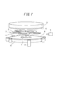
- FIG. 1A is a schematic perspective view of a wafer double-side polishing apparatus according to an embodiment of the present invention.
- FIG. (b) (c) is a figure which shows a mode that the temperature of the outer edge part of a carrier plate is measured using the double-side polish apparatus of (a).
- FIG. 8 is an enlarged view of a part of FIG. It is a figure which shows the relationship between grinding
- polishing It is a figure which shows the relationship between polishing time and the amplitude of the temperature of a carrier plate.
- this double-side polishing apparatus has one or a plurality of, in the illustrated example, five carrier plates 3 each having a holding hole 2 for holding a wafer 1, and these carrier plates 3 are placed thereon.
- a lower surface plate 4 and an upper surface plate 5 paired with the lower surface plate 4 are provided.
- a polishing pad 6 is affixed to each of the opposing surfaces of the upper and lower surface plates 4 and 5.
- the carrier plate 3 is rotatable. In the illustrated example, each carrier plate 3 can be rotated by the sun gear 7 and the internal gear 8.
- the carrier plate 3 has one or more holding holes 2, one in the illustrated example, and the holding holes 2 are eccentric with respect to the center of the carrier plate 3.
- the polishing apparatus includes a temperature measuring means 9 that measures the temperature of the carrier plate 3.
- the inventors performed double-side polishing of the wafer with the apparatus shown in FIG. 1, measured the temperature of the polishing slurry during polishing, and investigated the correlation with the polishing amount. As a result, the expected correlation was obtained. It was not reached. That is, it has been found that the temperature and the reproducibility of the polishing slurry is not good because it is affected by the discharge route.
- the inventors noticed that the temperature change of the polishing slurry was due to the temperature change of the constituent members of the polishing apparatus. Therefore, the temperature of the drainage tank disposed around the carrier plate 3, the upper surface plate 5, and the upper and lower surface plates was measured as a component of the polishing apparatus, and the relationship with the polishing time was evaluated.
- thermotracer manufactured by NEC Sanei Co., Ltd. was used, the wavelength was 8 to 14 ⁇ m, the sampling period was 10 s, and each component was measured from one direction.
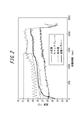
- FIG. 2 shows the temperature change of each constituent member depending on the polishing time.
- the carrier plate had a higher temperature during polishing than the drainage tank and the upper surface plate.
- the temperature of the carrier plate is characterized by having a remarkable periodicity synchronized with the rotation of the carrier plate in the initial stage of polishing, and the temperature becomes higher as the polishing time elapses. The knowledge that it was hard to be influenced by external factors was also obtained.
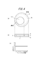
- FIG. 3 shows (a) the temperature distribution of the outer edge 3a of the carrier plate 3 at the initial stage of polishing, (b) the contact state between the wafer 1 and the carrier plate 3 and the polishing pad 6, and (c) the carrier plate. It is the figure which showed the pressure concerning a site
- the outer edge portion 3a refers to a region up to 30 mm radially inward from the outer edge end portion of the carrier plate. As shown in FIG.
- the wafer 1 is held in the holding hole 2 of the carrier plate 3, and the center of the wafer 1 is eccentric with respect to the center of the carrier plate 3.
- the elasticity of the polishing pad 6 causes the polishing pad 6 and the carrier plate 3 to The outer edge 3a of the part comes into strong contact.
- the pressure that the carrier plate 3 receives from the polishing pad 6 increases as the distance from the wafer 1 increases. For this reason, as shown in FIG. 3 (a), due to frictional heat generated by sliding between the portion in the vicinity of the contact portion and the polishing pad 6, the contact portion becomes higher in temperature than the other portions.
- the heat of the wafer 1 is easily conducted to the carrier plate 3, and the temperature rise of the carrier plate 3 due to this heat cannot be ignored.
- the temperature difference in the direction is reversed from the state shown in FIG. 3 (b). That is, among the portions of the carrier plate 3, the portion 3a, which is relatively hotter than the other portions at the initial stage of polishing, is relatively cooler than the other portions after the state shown in FIG. On the other hand, in the initial stage of polishing, the portion that is relatively cooler than the other portions becomes relatively hotter than the other portions after the state shown in FIG. 4 (b).
- the periodicity will be discussed. For example, when the temperature of the carrier plate is measured from one direction by optical means, the temperature of the carrier plate 3 is measured in the circumferential direction as the carrier plate 3 rotates. Therefore, in the initial stage of polishing, a periodic temperature change of the carrier plate 3 appears in synchronization with the rotation period of the carrier plate 3. As shown in FIG. 2, this periodicity decreases as polishing progresses, and as the thickness of the wafer 1 approaches the thickness of the carrier plate 3, the periodicity of temperature change disappears. After that, as the polishing proceeds, as described above, the heat transfer from the wafer 1 to the carrier plate 3 cannot be ignored, so the portion of the carrier plate 3 that is near the distance from the wafer is the initial polishing.
- Such reversal of the high temperature portion of the carrier plate means that the phase of the vibration component is reversed when the temperature of the carrier plate measured in the circumferential direction is decomposed into a direct current component and a vibration component. Therefore, the inventors have obtained the knowledge that the temperature of the carrier plate, in particular, the phase of the vibration component of the temperature of the carrier plate measured in the circumferential direction is a good index indicating the polishing state of the wafer.
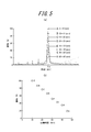
- Fig. 5 (a) shows the change in temperature of the carrier plate shown in Fig. 2, and the polishing time (10 to 45 min) is equally divided into eight time regions (A to H) in order to clarify the characteristics related to the period.
- a to H the amplitude of the vibration component of the temperature of the carrier plate is obtained by Fourier transform, and the graph showing the amplitude in the period axis domain is shown for each time domain.
- each time region has a peak value of amplitude in the vicinity of the value T0 of the rotation period of the carrier plate.
- FIG. 5 (b) is a diagram in which the peak value of the amplitude in each time region is plotted. As shown in FIG.
- the inventors have determined that the temperature of the carrier plate during polishing is higher than that of other components, and the temperature of the carrier plate determines the contact state between the carrier plate and the polishing pad, in other words, the thickness of the wafer. It was found that it was a good index to show. Therefore, it has been found here that by measuring the temperature of the carrier plate, the measured temperature of the carrier plate is associated with the polishing amount, the polishing amount can be accurately controlled, and the target wafer thickness can be achieved. It is. As described above, it is particularly effective to control the polishing amount by grasping the temperature phase and amplitude of the carrier plate.
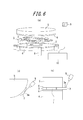
- FIG. 6 (a) is a schematic perspective view showing a wafer double-side polishing apparatus according to one embodiment of the present invention.
- the double-side polishing apparatus of the present invention in addition to the configuration of the double-side polishing apparatus provided with the temperature measuring means 9 for measuring the temperature of the carrier plate 3 shown in FIG.
- Control means 10 is also provided for controlling the polishing amount of the wafer in accordance with the measured temperature.
- the double-side polishing apparatus of the present invention includes a carrier plate 3 having one or more holding holes in the illustrated example.
- the holding hole 2 provided in the carrier plate is eccentric with respect to the center of the carrier plate 3.
- the term “eccentric” means that at least one center of the holding hole is separated from the center of the carrier plate. Specifically, when the carrier plate has two or more holding holes, the carrier plate is always decentered regardless of the arrangement, and when it has only one holding hole, the holding hole is concentric with the carrier plate. If it is not arranged in.
- the wafer 1 is held in the holding hole 2 and the carrier plate is rotated between the upper surface plate 5 and the lower surface plate 4 while supplying the polishing slurry, whereby the wafer 1 and the upper surface plate are fixed.
- the plates 4 and 5 are relatively slid to polish the front and back surfaces of the wafer 1 simultaneously.
- the upper and lower surface plates 4 and 5 can also be rotated. In this case, the upper and lower surface plates 4 and 5 are rotated in directions opposite to each other.
- the temperature of the carrier plate 3 is measured by the temperature measuring means 9, and the wafer 1 is controlled by the control means 10 based on the measured temperature of the carrier plate 3. It is important to control the amount of polishing.
- the temperature of the carrier plate 3 is measured by the temperature measuring means 9, the measured temperature of the carrier plate 3 is made to correspond to the polishing amount, and the polishing amount of the wafer 1 is controlled to an arbitrary target polishing amount by the control means 10. can do.
- the phase of the temperature of the carrier plate is obtained, for example, the phase change is associated with the polishing amount of the wafer, the polishing end point is determined, and the polishing amount is controlled. it can.
- FIG. 7 is a diagram showing the results of performing double-side polishing of the wafer with the apparatus shown in FIG. 1 and measuring the temperature of the carrier plate during polishing.
- the solid line graph in FIG. 8 is an enlarged view of the section of the polishing time of 500 to 600 (s) in FIG. Note that the temperature measurement results shown in FIGS. 7 and 8 are obtained when a temperature sensor of FT-H30 manufactured by Keyence Corporation is used as the temperature measurement means 9 and the wavelength is 8 to 14 ⁇ m and the sampling period is 500 ms.
- the temperature of the carrier plate has a vibration component synchronized with the rotation of the carrier plate. Therefore, the polishing state can be detected by obtaining the phase of the vibration component.
- the phase of the vibration component is not particularly limited.
- the temperature of the carrier plate (solid line graph in FIG. 8) is modeled as shown in the following formula (approximate to the broken line graph in FIG. 8), and the minimum It can be obtained by calculating the parameters A, B, C, and D by the square method.
- Equation 1 below the first and second terms on the right side are vibration components, and the third and fourth terms are direct current components.
- T Asin ( ⁇ t) + Bcos ( ⁇ t) + Ct + D
- ⁇ (2 ⁇ / 60) ⁇ r
- amplitude is (A 2 + B 2 ) 1/2
- the amplitude and phase can be calculated by a technique such as FFT (Fast Fourier Transform).
- the thickness of the wafer relative to the thickness of the carrier plate can be detected by determining the phase of the vibration component of the carrier plate as described above. For example, if the phase at which the wafer thickness and carrier plate thickness are equal is 90 degrees ( ⁇ / 2) from the phase at the start of polishing, the wafer thickness is thicker than the carrier plate thickness. When the time point is the target of the polishing amount at the end of polishing, the polishing is ended before the phase change reaches 90 degrees ( ⁇ / 2). On the other hand, when polishing until the thickness of the wafer becomes thinner than the thickness of the carrier plate, after the phase change reaches 90 degrees ( ⁇ / 2), the polishing corresponding to the target polishing amount is further performed. It is only necessary to set the time and continue polishing for the set polishing time.
- the amplitude of the temperature of the carrier plate is obtained, and for example, the change in the amplitude is associated with the polishing amount to determine the polishing end point, and the polishing amount can be controlled.
- the amplitude of the temperature of the carrier plate can be obtained, for example, by calculating the parameters of the modeled equation by the least square method, or can be obtained, for example, by FFT (Fast Fourier Transform). However, it is not limited to these methods.
- the above linear attenuation relationship of the amplitude is obtained. It is possible to accurately control the polishing amount. That is, when the target of the polishing amount at the end of polishing is the time when the thickness of the wafer is thicker than the thickness of the carrier plate, the polishing can be ended before the amplitude reaches the minimum value.
- polishing until the thickness of the wafer becomes thinner than the thickness of the carrier plate after the amplitude becomes the minimum value, a polishing time corresponding to the target polishing amount is set, and the amount of polishing time set is set. Only polishing can be continued.
- FIG. 9 is a diagram showing the relationship between the polishing time and the amplitude and phase of the vibration component of the temperature of the carrier plate shown in FIG. 7 by the least square method.
- the amplitude is shown as a relative value when the amplitude at the start of polishing is 1.
- the phase broken line
- the phase has a large change in the vicinity because the phase is inverted when the thickness of the wafer and the thickness of the carrier plate become substantially equal.
- the amplitude gradually decreases as the thickness of the wafer approaches the thickness of the carrier plate. For this reason, when the target polishing amount at the end of polishing is set at a time when the thickness of the wafer and the thickness of the carrier plate are equal, it is preferable to use amplitude as an index. In addition, when the target polishing amount at the end of polishing is set at a time when the thickness of the wafer becomes thinner than the thickness of the carrier plate, it is preferable to use a phase as an index. Furthermore, using both phase and amplitude as indices, for example, setting a phase change reference and an amplitude change reference corresponding to the target polishing amount, and polishing ends when both criteria are met. can do.
- both the phase and the amplitude are used as indices, for example, the phase change reference and the amplitude change reference corresponding to the target polishing amount are set, and the polishing is performed when one of the criteria is satisfied. By terminating the process, overpolishing can be further prevented.
- the temperature measuring means 9 for example, an optical means such as an infrared sensor can be used.
- the temperature of the carrier plate 3 is measured by measuring the side surface of the carrier plate 3 by installing the temperature measuring means 9 at the same height as the carrier plate 3.
- the temperature measuring means 9 is arranged above the upper surface plate, and the outer edge 3a of the carrier plate 3 protrudes radially outward from the outer edge of the upper and lower surface plates.
- the temperature of the outer edge portion 3a of the carrier plate thus projected can be measured by the temperature measuring means 9. Thereby, the temperature of a carrier plate can be measured correctly, without receiving the disturbance of the radiant heat from an upper and lower surface plate.
- the calculation of the amplitude and its peak value may be performed by processing the control means 10 from the temperature measured by the temperature measurement means 9, or by providing a calculation means in the temperature measurement means 9. Also good. Further, another calculation means may be interposed between the temperature measurement means 9 and the control means 10.
- the carrier plate whose temperature is to be measured is, for example, stainless steel (SUS) or fiber reinforced plastic in which a reinforcing fiber such as glass fiber, carbon fiber, or aramid fiber is combined with a resin such as epoxy, phenol, or polyimide. Any material can be used, and the surface of these materials coated with diamond-like carbon can also be used so as to improve wear resistance.
- SUS stainless steel
- fiber reinforced plastic in which a reinforcing fiber such as glass fiber, carbon fiber, or aramid fiber is combined with a resin such as epoxy, phenol, or polyimide. Any material can be used, and the surface of these materials coated with diamond-like carbon can also be used so as to improve wear resistance.
- an average of the temperature of the carrier plate 3 can be taken for each rotation period of the carrier plate 3. That is, if the average of the temperature for each rotation period of the carrier plate 3 is taken, the temperature of the carrier plate 3 increases monotonously. Therefore, the increase in the temperature of the carrier plate 3 can be accurately correlated with the increase in the polishing amount. Thus, the polishing end point can be detected, and the polishing amount of the wafer can be accurately controlled.
- the time when the thickness of the wafer becomes equal to the thickness of the carrier plate is defined as the time when the rate of increase of the temperature of the carrier plate per unit time becomes below a certain level, and the temperature of the carrier plate is It can be associated with the polishing amount. Also in this case, a desired polishing amount can be achieved by measuring the temperature of the carrier plate and using the measured temperature as an index. In addition, instead of the average value of the temperature of the carrier plate for each rotation period of the carrier plate, for example, the maximum value of the temperature of the carrier plate for each rotation period of the carrier plate is taken, and this maximum value is used as an index of the polishing amount. You can also.
- Example 1 In order to confirm the effect of the present invention, a test for evaluating the relationship between the phase of the temperature of the carrier plate and the thickness and shape of the wafer was performed by changing the polishing time.
- the polishing time was 5 levels with the polishing time changed between 29 and 32 minutes.
- a 300 mm diameter, crystal orientation (100), p-type silicon wafer was used as a wafer to be polished.
- As the carrier plate a glass fiber reinforced plastic (GFRP) plate in which glass fiber was compounded with an initial epoxy resin having a thickness of 745 ⁇ m was used.
- the center of the wafer was decentered 30 mm from the center of the carrier plate.
- FIG. 10 shows the result of the phase of the carrier plate at the end of polishing for each level with the polishing time changed.
- FIG. 10 shows the phase at the end of polishing on the vertical axis as a relative value when the phase is 0 when the polishing time is 100 seconds.
- FIG. 11 shows the relationship between the phase change and the wafer thickness at the end of polishing, and the relationship between the phase and the SFQR (Site Front least Quares Range) in the vicinity of the outer periphery of the wafer.
- SFQR is an index indicating the flatness of the outer peripheral portion of the wafer according to the SEMI standard. Specifically, this SFQR acquires a plurality of rectangular samples of a predetermined size from a wafer, and calculates the sum of the absolute values of the maximum displacements from the reference plane obtained by the least square method for each acquired sample. Is what you want.
- FIG. 11 shows the relationship between the phase change and the wafer thickness at the end of polishing, and the relationship between the phase and the SFQR (Site Front least Quares Range) in the vicinity of the outer periphery of the wafer.
- the SFQR on the vertical axis and the phase at the end of polishing on the horizontal axis are SFQR at the end of polishing when the polishing time is 30.5 minutes, and the phase after 100 seconds from the start of polishing is 0.
- the relative value is shown.
- SFQR means that the smaller the value, the better the flatness.
- the phase at the end of polishing decreases, and the amount of phase change from the start of polishing becomes ⁇ / 2 or more.
- the periodicity of the temperature change disappears, and then the phase is reversed by the above-described reversal of the high temperature portion.
- FIG. 11 it can be seen that as the phase at the end of polishing changes, SFQR decreases and the flatness of the outer edge of the wafer is improved. Therefore, the temperature of the carrier plate can be measured, and the phase of the temperature of the carrier plate can be correlated with the polishing amount. By determining the end of polishing using this correspondence, the wafer can be made to have a desired flatness. It can be seen that the polishing amount can be accurately controlled.
- Example 2 The same test as in Example 1 was performed except that the polishing time was changed to five levels of “30, 35, 40, 45, 50 (min)”.
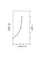
- FIG. 12 shows the result of the amplitude of the carrier plate at the end of polishing for each level with the polishing time changed. In FIG. 12, the amplitude at the end of polishing on the vertical axis is shown as a relative value when the amplitude at the end of polishing is 100 when the polishing time is 30 minutes.
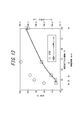
- FIG. 13 shows the relationship between the amplitude and the wafer thickness at the end of polishing, and the relationship between the amplitude and the SFQR in the vicinity of the wafer outer periphery. In FIG.
- the SFQR on the vertical axis and the amplitude at the end of polishing on the horizontal axis are relative values when the amplitude at the end of polishing when the polishing time is 30 min and the amplitude at the end of polishing is 100 respectively. Show. Therefore, SFQR means that the smaller the value, the higher the flatness.
- the amplitude at the end of polishing decreases as the polishing time increases. This means that the periodicity of temperature change disappears as the thickness of the wafer approaches the thickness of the carrier plate. Furthermore, as shown in FIG. 13, when the amplitude at the end of polishing is reduced, SFQR is reduced and the flatness of the outer edge of the wafer is improved. Therefore, the temperature of the carrier plate can be measured, and the amplitude of the temperature of the carrier plate can be associated with the polishing amount. By determining the end of polishing using this correspondence, the wafer can be made to have a desired flatness. It can be seen that the polishing amount can be accurately controlled.
- Example 3 In order to confirm that the effect of the present invention is effective regardless of the material of the carrier plate, a test for evaluating the relationship between the polishing time and the amplitude of the temperature of the carrier plate using three types of carrier plates of different materials. went.
- the three types of materials were those in which the carrier plate was made of GFRP, the carrier plate made of GFRP was coated with diamond-like carbon, and the carrier plate made of SUS was coated with diamond-like carbon.
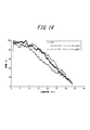
- the initial thickness of the carrier plate made of GFRP is 745 ⁇ m, polishing time is 30 minutes, (2) The initial thickness of the carrier plate made by applying diamond-like carbon to the carrier plate made of GFRP is 746 ⁇ m The polishing time was 32 minutes, (3) the initial thickness of the carrier plate in which diamond-like carbon was applied to a SUS carrier plate was 754 ⁇ m, and the polishing time was 34 minutes. Other conditions are the same as in Example 2. FIG. 14 shows the evaluation results.
- the amplitude decreases with the progress of polishing regardless of the material of the carrier plate, and there is a substantially linear correlation. Therefore, it can be seen that the temperature of the carrier plate can be measured for a carrier plate of any material, and the polishing amount of the wafer can be accurately controlled based on the measured temperature.
- Example 4 As a comparative example, using a carrier plate 3 in which the holding holes 2 are provided concentrically with the carrier plate 3 as shown in FIG. 15, the temperature of the carrier plate 3 during polishing is measured, and the temperature of the carrier plate 3 is measured. A test was conducted to evaluate the transition of the amplitude of the steel with the periodicity and the polishing time.
- the carrier plate was made of GFRP and had an initial thickness of 745 ⁇ m, and the polishing time was 30 (min). Other conditions are the same as in Example 2.
- FIG. 16 is a diagram showing the relationship between the polishing time and the peak value of the amplitude of the temperature of the carrier plate.
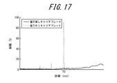
- FIG. 17 is a diagram showing the periodicity of the temperature of the carrier plate.
Landscapes
- Engineering & Computer Science (AREA)
- Mechanical Engineering (AREA)
- Mechanical Treatment Of Semiconductor (AREA)
- Finish Polishing, Edge Sharpening, And Grinding By Specific Grinding Devices (AREA)
- Constituent Portions Of Griding Lathes, Driving, Sensing And Control (AREA)
Abstract
Description
特に近年、半導体素子の微細化と、半導体ウェーハの大口径化により、露光時における半導体ウェーハの平坦度要求が厳しくなってきているという背景から、ウェーハの研磨量を適切に制御する手法が強く希求されている。
その結果、両面研磨装置においてウェーハを保持するキャリアプレートの温度がウェーハの研磨量の正確な指標となることを新たに見出し、キャリアプレートの温度を計測することにより、目標とする研磨量を達成するための研磨量の制御を正確に行うことができることの新規知見を得た。
(1) ワークを保持する保持孔を1つ以上有し、該保持孔の少なくとも1つが偏心して配置されるキャリアプレートにワークを保持し、研磨スラリーを供給しながら、研磨パッドが貼付された上定盤及び下定盤の間で少なくとも前記キャリアプレートを回転させることにより、前記ワークの表裏面を同時に研磨する方法において、
前記キャリアプレートの温度を測定し、測定されたキャリアプレートの温度の変化に基づき、前記ワークの研磨量を制御することを特徴とする、ワークの研磨方法。
ここで、「キャリアプレートの温度変化から算出される位相」とは、ワークの両面研磨時におけるキャリアプレートの回転に同期した、キャリアプレートの温度の振動成分の位相を意味する。キャリアプレートの温度の振動成分、及び当該振動成分の位相の算出方法としては、後述のFFT(高速フーリエ変換)やモデル化による最小二乗法による算出方法などがあるが、特に、これらに限定されない。
ここで、「キャリアプレートの温度変化から算出される振幅」とは、ワークの両面研磨時におけるキャリアプレートの回転に同期した、キャリアプレートの温度の振動成分の振幅を意味する。キャリアプレートの温度の振動成分、及び当該振動成分の振幅の算出方法としては、後述のFFT(高速フーリエ変換)やモデル化による最小二乗法による算出方法などがあるが、特に、これらに限定されない。
前記キャリアプレートの温度を測定する手段と、
測定した温度に応じてウェーハの研磨量を制御する制御手段と、をさらに備えていることを特徴とする、ワークの研磨装置。
また、研磨量の正確な制御によって、研磨不足による再研磨の必要がなくなり、ウェーハ製造工程における生産性が向上する。
さらに、所期した磨耗量を超えることもなくなるため、ウェーハ不良の発生やキャリアプレートの磨耗を防止することもできる。
発明者らは、上述した従前のトルク変化に基づくウェーハの研磨量の制御が不十分であることから、これに代わる手段について鋭意模索した。その結果、研磨末期における状態変化がスラリー温度において顕著であることから、ウェーハの研磨量の指標として、研磨装置の各部及び供給材(スラリー)等の研磨中の何某かの温度変化が適合する可能性に着目した。
そこで、まず、発明者らは、研磨装置の各部及び供給材の温度を測定するために、図1に示す研磨装置を試作した。
図1に示すように、この両面研磨装置は、ウェーハ1を保持する保持孔2を有する、1枚又は複数枚の、図示例で5枚のキャリアプレート3と、これらキャリアプレート3を載置する下定盤4と、下定盤4と対をなす上定盤5とを備えている。
上下定盤4、5の対向面には、それぞれ研磨パッド6が貼布されている。
また、キャリアプレート3は、回転可能である。図示例では、サンギア7とインターナルギア8とによって、各キャリアプレート3を回転させることができる。
キャリアプレート3は、保持孔2を1つ以上、図示例では1つ有しており、当該保持孔2は、キャリアプレート3の中心に対して偏心している。
さらに、この研磨装置は、キャリアプレート3の温度を測定する温度計測手段9を備えている。
次に、発明者らは、研磨スラリーの温度変化が、そもそも研磨装置の構成部材の温度変化によるものであることに着目した。そこで、研磨装置の構成部材として、キャリアプレート3、上定盤5、上下定盤の周囲に配設した排水槽の温度を測定し、研磨時間との関係を評価した。なお、温度計測手段9としては、NEC三栄社製サーモトレーサを用い、波長8~14μm、サンプリング周期10sとし、各構成部材を一方向から計測した。
各構成部材の研磨時間による温度変化を図2に示す。
図3は、研磨初期での、(a)キャリアプレート3の外縁部3aの温度分布の様子、(b)ウェーハ1及びキャリアプレート3と、研磨パッド6との接触状態、(c)キャリアプレートの部位にかかる圧力をウェーハからの距離との関係で示した図である。
ここで、外縁部3aとは、キャリアプレートの外縁端部から径方向内側に30mmまでの領域をいう。
図3(a)に示すように、ウェーハ1は、キャリアプレート3の保持孔2に保持されており、ウェーハ1の中心は、キャリアプレート3の中心に対して偏心している。
ここで、図3(b)に示すように、研磨初期においては、ウェーハ1の厚さはキャリアプレート3の厚さよりも厚いため、研磨パッド6の弾性により、研磨パッド6とキャリアプレート3の一部の外縁部3aが強く接触する。特に、図3(c)に示すように、キャリアプレート3が研磨パッド6から受ける圧力は、ウェーハ1からの距離が離れるほど大きくなる。このため、当該接触部分付近の部位と研磨パッド6との摺動による摩擦熱により、図3(a)に示すように、当該接触部位が他の部分と比較して高温になる。
しかし、図3(b)に示す状態においては、ウェーハ1がキャリアプレート3より厚いため、隙間Gが生じるのに対し、研磨が進行して、図4(b)に示す状態になると、ウェーハ1とキャリアプレート3の厚さが等しくなるため、この隙間がなくなる。
従って、ウェーハ1が有する熱がキャリアプレート3へ伝導しやすくなり、この熱によるキャリアプレート3の昇温が無視できなくなる。
そして、キャリアプレート3の部分のうち、ウェーハ1からの距離が近い部分ほど、温度が高くなる。
つまり、図4(b)に示す状態以降の研磨段階では、キャリアプレート3と研磨パッド6との接触状態が均一になる一方で、ウェーハ1から熱の伝導が無視できなくなるため、キャリアプレートの周方向の温度差は、図3(b)に示す状態から反転することとなる。すなわち、キャリアプレート3の部分のうち、研磨初期において、相対的に他の部分より高温であった部分3aは、図4(b)に示す状態以降では、他の部分より相対的には低温となり、一方で、研磨初期において、他の部分より相対的に低温であった部分は、図4(b)に示す状態以降では、他の部分より相対的に高温となるのである。
キャリアプレートの温度を、例えば一方向から光学的手段によって測定すると、キャリアプレート3の回転と共に、キャリアプレート3の温度を周方向に測定することになる。
従って、研磨初期においては、キャリアプレート3の回転の周期と同期した、キャリアプレート3の周期的温度変化があらわれることになる。この周期性は、図2に示すように、研磨が進行するにつれて小さくなり、ウェーハ1の厚さがキャリアプレート3の厚さに近づくにつれて、温度変化の周期性が消失する。
その後、研磨が進行するに従い、上述したように、ウェーハ1からキャリアプレート3への熱の伝達が無視できなくなるため、キャリアプレート3の部分のうち、ウェーハからの距離が近い部分が、研磨初期とは反対に、より高温となり、キャリアプレートの温度変化の周期性が再びあらわれ始める。
このような、キャリアプレートの高温箇所の反転は、周方向に測定したキャリアプレートの温度を、直流成分と振動成分とに分解した際に、当該振動成分の位相が反転することを意味する。
従って、発明者らは、キャリアプレートの温度、特に、周方向に測定したキャリアプレートの温度の振動成分の位相が、ウェーハの研磨状態を示す良い指標となるという知見を得たものである。
図5(a)は、図2に示したキャリアプレートの温度変化について、その周期に関する特性を明らかにすべく、研磨時間(10~45min)を8つの時間領域(A~H)に等分して、各時間領域A~Hにおいて、フーリエ変換によりキャリアプレートの温度の振動成分の振幅を求め、振幅を周期軸領域で表示したグラフを、上記時間領域ごとに示した図である。
図5(a)に示すように、各時間領域で、キャリアプレートの回転の周期の値T0の付近において振幅のピーク値を有する。
図5(b)は、各時間領域の振幅のピーク値をプロットした図である。図5(b)に示すように、振幅のピーク値は、研磨時間の増大に伴い、ほぼ線形に減衰していくことがわかった。
なお、図5(a)(b)において、縦軸の振幅は、時間領域A(8~10min)における振幅のピーク値を100(%)としたときの相対値で示している。
従って、発明者らは、周方向に測定したキャリアプレートの温度の振幅も、ウェーハの研磨状態を示す良い指標となるという知見を得たものである。
従って、キャリアプレートの温度を測定することにより、測定したキャリアプレートの温度と研磨量とを対応付けて、研磨量を正確に制御し、目標とするウェーハの厚さを達成できることをここに見出したのである。
先に説明したように、特に、キャリアプレートの温度の位相や振幅を把握することにより、研磨量を制御することが有効である。
図6(a)に示すように、本発明の両面研磨装置は、上述の、図1に示した、キャリアプレート3の温度を測定する温度計測手段9を備えた両面研磨装置の構成に加え、測定した温度に応じてウェーハの研磨量を制御する制御手段10も備えている。
また、本発明の両面研磨装置は、1つ以上、図示例では1つの保持孔を有するキャリアプレート3を備えている。キャリアプレートに設けた保持孔2は、キャリアプレート3の中心に対して偏心している。
なお、ここでいう偏心しているとは、保持孔の少なくとも1つの中心がキャリアプレートの中心に対して離間していることをいう。具体的には、キャリアプレートが保持孔を2つ以上有している場合は、それらの配置によらずに必ず偏心し、保持孔を1つのみ有する場合は、保持孔がキャリアプレートと同心円状に配置されていなければよい。
なお、図1に示すように、上下定盤4、5も回転させることができ、この場合、上下定盤4、5は互いに反対方向に回転させる。
ここで、本発明の両面研磨方法においては、ウェーハ1の研磨中において、温度計測手段9によりキャリアプレート3の温度を測定し、測定されたキャリアプレート3の温度に基づき、制御手段10によってウェーハ1の研磨量を制御することが肝要である。
そこで、上記振動成分の位相を求めることにより研磨状態を検出することができる。
上記振動成分の位相は、特には限定しないが、例えば、キャリアプレートの温度(図8の実線のグラフ)を、以下の式のようにモデル化(図8の破線のグラフに近似)し、最小二乗法により、パラメータA、B、C、Dを算出することにより求めることができる。なお、下記の式1においては、右辺の第1項及び第2項が振動成分であり、第3項及び第4項が直流成分である。
(式1)
T=Asin(αt)+Bcos(αt)+Ct+D
(式2)
α=(2π/60)×r
ただし、rはキャリアプレートの回転速度であり、振幅は (A2+B2)1/2、位相θはsin-1θ=B/(A2+B2)1/2もしくはcos-1θ=A/(A2+B2)1/2で算出される。
また、例えば、FFT(高速フーリエ変換)等の手法によっても振幅および位相を算出することができる。
具体的には、上述のように、キャリアプレートの温度の振幅を求め、例えば、この振幅の変化を研磨量と対応させて、研磨終了時点を判断し、研磨量の制御を行うことができる。
すなわち、ウェーハの厚さがキャリアプレートの厚さより厚い時点を研磨終了時における研磨量の目標とする場合は、上記振幅が極小値となる前に研磨を終了することができる。一方で、ウェーハの厚さがキャリアプレートの厚さより薄くなるまで研磨する場合には、振幅が極小値となった後、さらに目標の研磨量に相当する研磨時間を設定し、設定した研磨時間分だけ研磨を続行することができる。
図9は、図7に示すキャリアプレートの温度の振動成分の振幅及び位相を、最小二乗法により求め、研磨時間との関係を示した図である。
なお、振幅は研磨開始時における振幅を1としたときの相対値で示している。
図9に示すように、位相(破線)は、ウェーハの厚さとキャリアプレートの厚さとがほぼ等しくなる時点で、位相の反転が生じるため、この付近での変化が大きい。一方で、振幅(実線)は、ウェーハの厚さがキャリアプレートの厚さに近づくにつれて漸減していく。
このため、研磨終了時点での目標研磨量を、ウェーハの厚さとキャリアプレートの厚さとが等しくなる時点に設定する場合には、指標として振幅を用いることが好ましい。
また、研磨終了時点での目標研磨量を、ウェーハの厚さがキャリアプレートの厚さより薄くなる時点に設定する場合には、指標として位相を用いることが好ましい。
さらに、位相と振幅との双方を指標として用い、例えば、目標とする研磨量に対応する位相の変化の基準と振幅の変化の基準とを設定し、双方の基準を満たした時点で研磨を終了することができる。これにより、研磨不足を回避して再研磨にかかるコストや時間を削減することができる。あるいは、位相と振幅との双方を指標として用い、例えば、目標とする研磨量に対応する位相の変化の基準と振幅の変化の基準とを設定しつつも、一方の基準を満たした時点で研磨を終了することにより、過研磨をより一層防止することができる。
キャリアプレート3の温度の測定は、例えば、図1に示す場合のように、温度計測手段9をキャリアプレート3と同程度の高さに設置してキャリアプレート3の側面部を計測するほか、図6(a)(b)(c)に示すように、温度計測手段9を上定盤の上方に配置し、キャリアプレート3の外縁部3aを上下定盤の外縁より径方向外方に突出させて研磨を行い、突出させたキャリアプレートの外縁部3aの温度を温度計測手段9により測定することもできる。これにより、上下定盤からの輻射熱の外乱を受けることなく、キャリアプレートの温度を正確に測定することができる。
また、振幅及びそのピーク値の算出は、温度計測手段9によって計測された温度から制御手段10にて処理することにより行っても良いし、温度計測手段9内に算出手段を設けることにより行っても良い。さらに、温度計測手段9と制御手段10との間に、他の算出手段を介在させて行うこともできる。
すなわち、キャリアプレート3の自転周期毎の温度の平均をとれば、キャリアプレート3の温度が単調に増加するため、キャリアプレート3の温度の増加を研磨量の増加と対応付けておくことで、正確に研磨終了時点を検出することができ、ウェーハの研磨量を正確に制御することができる。
このとき、例えば、ウェーハの厚さがキャリアプレートの厚さと等しくなる時点を、キャリアプレートの温度の単位時間当たりの増加率が一定以下となった時点であると定義して、キャリアプレートの温度を研磨量と対応付けることができる。
この場合も、キャリアプレートの温度を測定し、測定した温度を指標とすることにより、所望の研磨量を達成することができる。
なお、キャリアプレートの自転周期毎のキャリアプレートの温度の平均値の代わりに、例えば、キャリアプレートの自転周期毎のキャリアプレートの温度の最大値をとり、この最大値を研磨量の指標とすることもできる。
本発明の効果を確かめるため、研磨時間を変えて、キャリアプレートの温度の位相と、ウェーハの厚さ及び形状との関係について評価する試験を行った。
研磨時間は、29~32分間の間で研磨時間を変更した5水準とした。
試験は、研磨に供するウェーハとして、直径300mm、結晶方位(100)、p型のシリコンウェーハを使用した。
キャリアプレートは、初期の厚さ745μmのエポキシ樹脂にガラス繊維を複合したガラス繊維強化プラスチック(GFRP:Glass Fiber Reinforced Plastics)のプレートを用いた。
ここで、ウェーハの中心は、キャリアプレートの中心と、30mm偏心させた。
図6(a)に示す構成の装置を用い、研磨パッドは、ニッタ・ハース社製発泡ウレタン研磨布MHN15、研磨スラリーは、ニッタ・ハース社製Nalco2350を用いた。上下定盤を互いに逆方向に回転させ、キャリアプレートを上定盤と同方向に回転させて、キャリアプレート内に装填したウェーハ表面を研磨した。
温度センサとしては、キーエンス社製FT-H30を用い、波長8~14μm、サンプリング周期500msとした。
図10に、研磨時間を変更した各水準毎の研磨終了時におけるキャリアプレートの位相の結果を示す。なお、図10において、縦軸の研磨終了時の位相は、研磨時間が100秒における位相を0としたときの相対値で示している。
また、図11に、研磨終了時における、位相変化とウェーハの厚さとの関係、および位相とウェーハ外周部近傍のSFQR(Site Front least sQuares Range)との関係を示す。
ここで、SFQRは、SEMI規格に係る、ウェーハの外周部の平坦度を示す指標である。このSFQRは、具体的には、ウェーハから所定寸法の矩形状のサンプルを複数取得し、取得した各サンプルについて最小二乗法により求められた基準面からの最大変位量の絶対値の和を算出することにより求めるものである。
なお、図11において、縦軸のSFQR及び横軸の研磨終了時の位相は、研磨時間が30.5分の場合の研磨終了時における、SFQRを100、研磨開始時から100秒後の位相を0としたときの相対値で示している。SFQRは、値が小さい方が平坦度が良好であることを意味する。
さらに、図11に示すように、研磨終了時の位相が変化するにつれ、SFQRが減少し、ウェーハ外縁部の平坦性が改善されることがわかる。
従って、キャリアプレートの温度を測定し、キャリアプレートの温度の位相を研磨量と対応付けることができ、この対応関係を用いて研磨終了時を判定することで、ウェーハを所望の平坦度にするための研磨量を正確に制御できることがわかる。
研磨時間を「30、35、40、45、50(min)」の5水準に変更した以外は、実施例1と同様の試験を行った。
図12に、研磨時間を変更した各水準毎の研磨終了時におけるキャリアプレートの振幅の結果を示す。なお、図12において、縦軸の研磨終了時の振幅は、研磨時間が30minの場合の研磨終了時における振幅を100としたときの相対値で示している。
また、図13に、研磨終了時における、振幅とウェーハの厚さとの関係、および振幅とウェーハ外周部近傍での上記SFQRとの関係を示す。
なお、図13において、縦軸のSFQR及び横軸の研磨終了時の振幅は、研磨時間が30minの場合の研磨終了時における、SFQR及び研磨終了時の振幅をそれぞれ100としたときの相対値で示している。従って、SFQRは、値が小さい方が平坦度が高いことを意味する。
さらに、図13に示すように、研磨終了時の振幅が小さくなると、SFQRが減少し、ウェーハ外縁部の平坦性が改善されることがわかる。
従って、キャリアプレートの温度を測定し、キャリアプレートの温度の振幅を研磨量と対応付けることができ、この対応関係を用いて研磨終了時を判定することで、ウェーハを所望の平坦度にするための研磨量を正確に制御できることがわかる。
本発明の効果がキャリアプレートの材質によらずに有効であることを確かめるため、材質の異なる3種類のキャリアプレートを用いて、研磨時間とキャリアプレートの温度の振幅との関係を評価する試験を行った。
3種類の材質は、キャリアプレートをGFRP製としたもの、GFRP製のキャリアプレートにダイヤモンドライクカーボンを塗布したもの、SUS製のキャリアプレートにダイヤモンドライクカーボンを塗布したものとした。
試験は、(1)GFRP製のキャリアプレートの初期の厚さは745μmで、研磨時間は30分、(2)GFRP製のキャリアプレートにダイヤモンドライクカーボンを塗布したキャリアプレートの初期の厚さは746μmで、研磨時間は32分、(3) SUS製のキャリアプレートにダイヤモンドライクカーボンを塗布したキャリアプレートの初期の厚さは754μmで、研磨時間は34分として行った。
その他の条件は実施例2と同様である。
図14に、評価結果を示す。
従って、任意の材質のキャリアプレートに対して、キャリアプレートの温度を測定し、測定した温度に基づいて、ウェーハの研磨量を正確に制御することができることがわかる。
比較例として、図15に示すような、保持孔2がキャリアプレート3と同心円状に設けられているキャリアプレート3を用い、研磨中のキャリアプレート3の温度を測定して、キャリアプレート3の温度の振幅の周期性及び研磨時間による推移について評価する試験を行った。
キャリアプレートはGFRP製で、初期の厚さが745μmのものを用い、研磨時間を30(min)とした。その他の条件は、実施例2と同様である。
図16は、研磨時間とキャリアプレートの温度の振幅のピーク値との関係を示す図である。
また、図17は、キャリアプレートの温度の周期性を示す図である。
2 保持孔
3 キャリアプレート
4 下定盤
5 上定盤
6 研磨パッド
7 サンギア
8 インターナルギア
9 温度測定手段
10 研磨量制御手段
G 隙間
Claims (7)
- ワークを保持する保持孔を1つ以上有し、該保持孔の少なくとも1つが偏心して配置されるキャリアプレートにワークを保持し、研磨スラリーを供給しながら、研磨パッドが貼付された上定盤及び下定盤の間で少なくとも前記キャリアプレートを回転させることにより、前記ワークの表裏面を同時に研磨する方法において、
前記キャリアプレートの温度を測定し、測定されたキャリアプレートの温度の変化に基づき、前記ワークの研磨量を制御することを特徴とする、ワークの研磨方法。 - 前記キャリアプレートの温度変化から算出される位相の変化に基づき、前記ワークの研磨量を制御する、請求項1に記載のワークの研磨方法。
- 前記キャリアプレートの温度変化から算出される振幅の変化に基づき、前記ワークの研磨量を制御する、請求項1に記載のワークの研磨方法。
- 前記キャリアプレートの温度変化から算出される、位相の変化と振幅の変化との双方に基づき、前記ワークの研磨量を制御する、請求項1に記載のワークの研磨方法。
- 前記キャリアプレートの外縁部を、前記上下定盤の外縁より径方向外方に突出させて研磨を行い、前記突出させたキャリアプレートの外縁部の温度を光学的温度計測手段により測定する、請求項1~4のいずれか一項に記載のワークの研磨方法。
- 研磨に供するワークを保持する1つ以上の保持孔が形成され、該保持孔の少なくとも1つが偏心して配置される、回転可能なキャリアプレートと、前記キャリアプレートを載置する下定盤及び、該下定盤と対をなす上定盤とを備えた、ワークの両面を研磨する装置において、
前記キャリアプレートの温度を測定する手段と、
測定した温度に応じてウェーハの研磨量を制御する制御手段と、をさらに備えていることを特徴とする、ワークの研磨装置。 - 前記温度計測手段は、光学的計測手段である、請求項6に記載のワークの研磨装置。
Priority Applications (5)
| Application Number | Priority Date | Filing Date | Title |
|---|---|---|---|
| SG2013045679A SG191150A1 (en) | 2010-12-27 | 2011-10-19 | Method and apparatus for polishing workpiece |
| KR1020137015040A KR101436485B1 (ko) | 2010-12-27 | 2011-10-19 | 작업물의 연마방법 및 연마장치 |
| JP2012550680A JP5527430B2 (ja) | 2010-12-27 | 2011-10-19 | ワークの研磨方法 |
| US13/976,205 US9707659B2 (en) | 2010-12-27 | 2011-10-19 | Method and apparatus for polishing workpiece |
| DE112011104610.3T DE112011104610B4 (de) | 2010-12-27 | 2011-10-19 | Verfahren und Vorrichtung zum Polieren eines Werkstücks |
Applications Claiming Priority (2)
| Application Number | Priority Date | Filing Date | Title |
|---|---|---|---|
| JP2010290353 | 2010-12-27 | ||
| JP2010-290353 | 2010-12-27 |
Publications (1)
| Publication Number | Publication Date |
|---|---|
| WO2012090366A1 true WO2012090366A1 (ja) | 2012-07-05 |
Family
ID=46382512
Family Applications (1)
| Application Number | Title | Priority Date | Filing Date |
|---|---|---|---|
| PCT/JP2011/005856 Ceased WO2012090366A1 (ja) | 2010-12-27 | 2011-10-19 | ワークの研磨方法及び研磨装置 |
Country Status (7)
| Country | Link |
|---|---|
| US (1) | US9707659B2 (ja) |
| JP (2) | JP5527430B2 (ja) |
| KR (1) | KR101436485B1 (ja) |
| DE (1) | DE112011104610B4 (ja) |
| SG (1) | SG191150A1 (ja) |
| TW (1) | TWI498958B (ja) |
| WO (1) | WO2012090366A1 (ja) |
Cited By (2)
| Publication number | Priority date | Publication date | Assignee | Title |
|---|---|---|---|---|
| JP2017112302A (ja) * | 2015-12-18 | 2017-06-22 | 株式会社Sumco | ウェーハ研磨方法および研磨装置 |
| JP2019202373A (ja) * | 2018-05-22 | 2019-11-28 | 株式会社Sumco | ワークの両面研磨装置および両面研磨方法 |
Families Citing this family (7)
| Publication number | Priority date | Publication date | Assignee | Title |
|---|---|---|---|---|
| DE102012201465B4 (de) * | 2012-02-01 | 2018-01-18 | Wafios Ag | Verfahren zum Schleifen von Federenden und Federendenschleifmaschine |
| JP6707831B2 (ja) * | 2015-10-09 | 2020-06-10 | 株式会社Sumco | 研削装置および研削方法 |
| DE112017005728T5 (de) * | 2016-12-09 | 2019-08-29 | Shin-Etsu Handotai Co., Ltd. | Träger für doppelseitige Poliervorrichtung, doppelseitige Poliervorrichtung und doppelseitiges Polierverfahren |
| TWI825043B (zh) * | 2017-11-14 | 2023-12-11 | 美商應用材料股份有限公司 | 用於化學機械研磨的溫度控制的方法與系統 |
| CN110303423B (zh) * | 2018-03-20 | 2021-10-26 | 胜高股份有限公司 | 工件的研磨方法及研磨装置 |
| CN113560122A (zh) * | 2021-07-06 | 2021-10-29 | 北京理工大学 | 一种面向tsv的可偏心式旋涂一体化装置 |
| JP2025074660A (ja) * | 2023-10-30 | 2025-05-14 | 株式会社Sumco | ワークの研磨装置及び研磨方法 |
Citations (7)
| Publication number | Priority date | Publication date | Assignee | Title |
|---|---|---|---|---|
| JPH1034529A (ja) * | 1996-07-18 | 1998-02-10 | Speedfam Co Ltd | 自動定寸装置 |
| WO2000012263A1 (en) * | 1998-08-31 | 2000-03-09 | Micron Technology, Inc. | Method and apparatus for wireless transfer of chemical-mechanical planarization measurements |
| JP2000271857A (ja) * | 1999-03-25 | 2000-10-03 | Super Silicon Kenkyusho:Kk | 大口径ウェーハの両面加工方法及び装置 |
| JP2001353658A (ja) * | 2000-06-09 | 2001-12-25 | Mitsubishi Materials Corp | ウェーハ研磨装置及び研磨方法 |
| JP2003197586A (ja) * | 2001-12-28 | 2003-07-11 | Semiconductor Leading Edge Technologies Inc | Cmp装置、研磨パッド及び研磨方法 |
| JP2005005317A (ja) * | 2003-06-09 | 2005-01-06 | Sumitomo Mitsubishi Silicon Corp | 半導体ウェーハの研磨方法およびその研磨装置 |
| JP2008235899A (ja) * | 2007-03-19 | 2008-10-02 | Siltronic Ag | 複数の半導体ウェハを同時に研削するための方法 |
Family Cites Families (6)
| Publication number | Priority date | Publication date | Assignee | Title |
|---|---|---|---|---|
| US6375540B1 (en) * | 2000-06-30 | 2002-04-23 | Lam Research Corporation | End-point detection system for chemical mechanical posing applications |
| JP2002231672A (ja) | 2001-01-31 | 2002-08-16 | Mitsubishi Materials Silicon Corp | ウェーハ研磨方法およびその装置 |
| JP3991598B2 (ja) | 2001-02-26 | 2007-10-17 | 株式会社Sumco | ウエーハ研磨方法 |
| KR100506942B1 (ko) * | 2003-09-03 | 2005-08-05 | 삼성전자주식회사 | 화학적 기계적 연마장치 |
| DE102007013058B4 (de) * | 2007-03-19 | 2024-01-11 | Lapmaster Wolters Gmbh | Verfahren zum gleichzeitigen Schleifen mehrerer Halbleiterscheiben |
| JP5076723B2 (ja) * | 2007-08-09 | 2012-11-21 | 富士通株式会社 | 研磨装置、基板及び電子機器の製造方法 |
-
2011
- 2011-10-19 SG SG2013045679A patent/SG191150A1/en unknown
- 2011-10-19 JP JP2012550680A patent/JP5527430B2/ja active Active
- 2011-10-19 KR KR1020137015040A patent/KR101436485B1/ko active Active
- 2011-10-19 US US13/976,205 patent/US9707659B2/en active Active
- 2011-10-19 WO PCT/JP2011/005856 patent/WO2012090366A1/ja not_active Ceased
- 2011-10-19 DE DE112011104610.3T patent/DE112011104610B4/de active Active
- 2011-11-04 TW TW100140404A patent/TWI498958B/zh active
-
2014
- 2014-04-17 JP JP2014085626A patent/JP5708864B2/ja active Active
Patent Citations (7)
| Publication number | Priority date | Publication date | Assignee | Title |
|---|---|---|---|---|
| JPH1034529A (ja) * | 1996-07-18 | 1998-02-10 | Speedfam Co Ltd | 自動定寸装置 |
| WO2000012263A1 (en) * | 1998-08-31 | 2000-03-09 | Micron Technology, Inc. | Method and apparatus for wireless transfer of chemical-mechanical planarization measurements |
| JP2000271857A (ja) * | 1999-03-25 | 2000-10-03 | Super Silicon Kenkyusho:Kk | 大口径ウェーハの両面加工方法及び装置 |
| JP2001353658A (ja) * | 2000-06-09 | 2001-12-25 | Mitsubishi Materials Corp | ウェーハ研磨装置及び研磨方法 |
| JP2003197586A (ja) * | 2001-12-28 | 2003-07-11 | Semiconductor Leading Edge Technologies Inc | Cmp装置、研磨パッド及び研磨方法 |
| JP2005005317A (ja) * | 2003-06-09 | 2005-01-06 | Sumitomo Mitsubishi Silicon Corp | 半導体ウェーハの研磨方法およびその研磨装置 |
| JP2008235899A (ja) * | 2007-03-19 | 2008-10-02 | Siltronic Ag | 複数の半導体ウェハを同時に研削するための方法 |
Cited By (6)
| Publication number | Priority date | Publication date | Assignee | Title |
|---|---|---|---|---|
| JP2017112302A (ja) * | 2015-12-18 | 2017-06-22 | 株式会社Sumco | ウェーハ研磨方法および研磨装置 |
| JP2019202373A (ja) * | 2018-05-22 | 2019-11-28 | 株式会社Sumco | ワークの両面研磨装置および両面研磨方法 |
| WO2019225087A1 (ja) * | 2018-05-22 | 2019-11-28 | 株式会社Sumco | ワークの両面研磨装置および両面研磨方法 |
| KR20200133811A (ko) * | 2018-05-22 | 2020-11-30 | 가부시키가이샤 사무코 | 워크의 양면 연마 장치 및 양면 연마 방법 |
| JP7031491B2 (ja) | 2018-05-22 | 2022-03-08 | 株式会社Sumco | ワークの両面研磨装置および両面研磨方法 |
| KR102399968B1 (ko) | 2018-05-22 | 2022-05-18 | 가부시키가이샤 사무코 | 워크의 양면 연마 장치 및 양면 연마 방법 |
Also Published As
| Publication number | Publication date |
|---|---|
| TW201230184A (en) | 2012-07-16 |
| JP2014166677A (ja) | 2014-09-11 |
| US20130337723A1 (en) | 2013-12-19 |
| DE112011104610B4 (de) | 2020-03-26 |
| TWI498958B (zh) | 2015-09-01 |
| JPWO2012090366A1 (ja) | 2014-06-05 |
| JP5527430B2 (ja) | 2014-06-18 |
| SG191150A1 (en) | 2013-07-31 |
| KR101436485B1 (ko) | 2014-09-01 |
| US9707659B2 (en) | 2017-07-18 |
| JP5708864B2 (ja) | 2015-04-30 |
| DE112011104610T5 (de) | 2013-10-02 |
| KR20130088867A (ko) | 2013-08-08 |
Similar Documents
| Publication | Publication Date | Title |
|---|---|---|
| JP5708864B2 (ja) | ワークの研磨装置 | |
| JP5924409B2 (ja) | ワークの研磨方法およびワークの研磨装置 | |
| KR20150026930A (ko) | 워크의 양면 연마 장치 및 방법 | |
| JP6490818B2 (ja) | ウエハー研磨装置及びこれを用いたウエハー研磨方法 | |
| US9033764B2 (en) | Method of polishing object to be polished | |
| JP6579056B2 (ja) | ウェーハの両面研磨方法 | |
| TW201730951A (zh) | 晶圓研磨方法及研磨裝置 | |
| JP2010045279A (ja) | 半導体基板の両面研磨方法 | |
| JP6589762B2 (ja) | 両面研磨装置 | |
| KR20150039576A (ko) | 멤브레인, 연마 헤드, 워크의 연마 장치 및 연마 방법, 그리고, 실리콘 웨이퍼 | |
| WO2023035247A1 (zh) | 化学机械抛光设备及其控制方法 | |
| WO2017073265A1 (ja) | 半導体ウェーハの両面研磨方法及びその両面研磨装置 | |
| US9502318B2 (en) | Polish apparatus, polish method, and method of manufacturing semiconductor device | |
| CN110303423B (zh) | 工件的研磨方法及研磨装置 | |
| KR102386609B1 (ko) | 워크의 양면 연마 장치 및 양면 연마 방법 | |
| JP5699783B2 (ja) | ワークの研磨方法及び研磨装置 | |
| Fujita et al. | Pressure distribution control on surface conformable polishing in chemical mechanical planarization | |
| JP4326985B2 (ja) | ウエーハ研磨方法 | |
| KR100931787B1 (ko) | 양면 연마 공정에서 웨이퍼의 평탄도를 제어하는 방법 | |
| JP6973315B2 (ja) | ワークの両面研磨装置および両面研磨方法 | |
| TWI693123B (zh) | 工件的兩面研磨裝置及兩面研磨方法 | |
| KR20220047645A (ko) | 워크의 양면 연마 방법 | |
| JP6398939B2 (ja) | テンプレートの測定方法及び評価方法 | |
| JP2024024161A (ja) | ウェーハの片面研磨方法、ウェーハの製造方法、およびウェーハの片面研磨装置 |
Legal Events
| Date | Code | Title | Description |
|---|---|---|---|
| 121 | Ep: the epo has been informed by wipo that ep was designated in this application |
Ref document number: 11854313 Country of ref document: EP Kind code of ref document: A1 |
|
| WWE | Wipo information: entry into national phase |
Ref document number: 2012550680 Country of ref document: JP |
|
| ENP | Entry into the national phase |
Ref document number: 20137015040 Country of ref document: KR Kind code of ref document: A |
|
| WWE | Wipo information: entry into national phase |
Ref document number: 112011104610 Country of ref document: DE Ref document number: 1120111046103 Country of ref document: DE |
|
| WWE | Wipo information: entry into national phase |
Ref document number: 13976205 Country of ref document: US |
|
| 122 | Ep: pct application non-entry in european phase |
Ref document number: 11854313 Country of ref document: EP Kind code of ref document: A1 |