WO2012081623A1 - 表面検査装置及びその方法 - Google Patents
表面検査装置及びその方法 Download PDFInfo
- Publication number
- WO2012081623A1 WO2012081623A1 PCT/JP2011/078919 JP2011078919W WO2012081623A1 WO 2012081623 A1 WO2012081623 A1 WO 2012081623A1 JP 2011078919 W JP2011078919 W JP 2011078919W WO 2012081623 A1 WO2012081623 A1 WO 2012081623A1
- Authority
- WO
- WIPO (PCT)
- Prior art keywords
- detection signal
- wafer
- substrate
- pattern
- exposure
- Prior art date
- Legal status (The legal status is an assumption and is not a legal conclusion. Google has not performed a legal analysis and makes no representation as to the accuracy of the status listed.)
- Ceased
Links
Images





Classifications
-
- G—PHYSICS
- G01—MEASURING; TESTING
- G01N—INVESTIGATING OR ANALYSING MATERIALS BY DETERMINING THEIR CHEMICAL OR PHYSICAL PROPERTIES
- G01N21/00—Investigating or analysing materials by the use of optical means, i.e. using sub-millimetre waves, infrared, visible or ultraviolet light
- G01N21/84—Systems specially adapted for particular applications
- G01N21/88—Investigating the presence of flaws or contamination
- G01N21/95—Investigating the presence of flaws or contamination characterised by the material or shape of the object to be examined
- G01N21/9501—Semiconductor wafers
-
- G—PHYSICS
- G01—MEASURING; TESTING
- G01N—INVESTIGATING OR ANALYSING MATERIALS BY DETERMINING THEIR CHEMICAL OR PHYSICAL PROPERTIES
- G01N21/00—Investigating or analysing materials by the use of optical means, i.e. using sub-millimetre waves, infrared, visible or ultraviolet light
- G01N21/84—Systems specially adapted for particular applications
- G01N21/88—Investigating the presence of flaws or contamination
- G01N21/94—Investigating contamination, e.g. dust
-
- G—PHYSICS
- G01—MEASURING; TESTING
- G01N—INVESTIGATING OR ANALYSING MATERIALS BY DETERMINING THEIR CHEMICAL OR PHYSICAL PROPERTIES
- G01N21/00—Investigating or analysing materials by the use of optical means, i.e. using sub-millimetre waves, infrared, visible or ultraviolet light
- G01N21/84—Systems specially adapted for particular applications
- G01N21/88—Investigating the presence of flaws or contamination
- G01N21/95—Investigating the presence of flaws or contamination characterised by the material or shape of the object to be examined
- G01N21/956—Inspecting patterns on the surface of objects
- G01N21/95607—Inspecting patterns on the surface of objects using a comparative method
-
- G—PHYSICS
- G02—OPTICS
- G02B—OPTICAL ELEMENTS, SYSTEMS OR APPARATUS
- G02B26/00—Optical devices or arrangements for the control of light using movable or deformable optical elements
- G02B26/08—Optical devices or arrangements for the control of light using movable or deformable optical elements for controlling the direction of light
- G02B26/0808—Optical devices or arrangements for the control of light using movable or deformable optical elements for controlling the direction of light by means of one or more diffracting elements
-
- G—PHYSICS
- G03—PHOTOGRAPHY; CINEMATOGRAPHY; ANALOGOUS TECHNIQUES USING WAVES OTHER THAN OPTICAL WAVES; ELECTROGRAPHY; HOLOGRAPHY
- G03F—PHOTOMECHANICAL PRODUCTION OF TEXTURED OR PATTERNED SURFACES, e.g. FOR PRINTING, FOR PROCESSING OF SEMICONDUCTOR DEVICES; MATERIALS THEREFOR; ORIGINALS THEREFOR; APPARATUS SPECIALLY ADAPTED THEREFOR
- G03F7/00—Photomechanical, e.g. photolithographic, production of textured or patterned surfaces, e.g. printing surfaces; Materials therefor, e.g. comprising photoresists; Apparatus specially adapted therefor
- G03F7/70—Microphotolithographic exposure; Apparatus therefor
- G03F7/70216—Mask projection systems
- G03F7/70341—Details of immersion lithography aspects, e.g. exposure media or control of immersion liquid supply
-
- G—PHYSICS
- G03—PHOTOGRAPHY; CINEMATOGRAPHY; ANALOGOUS TECHNIQUES USING WAVES OTHER THAN OPTICAL WAVES; ELECTROGRAPHY; HOLOGRAPHY
- G03F—PHOTOMECHANICAL PRODUCTION OF TEXTURED OR PATTERNED SURFACES, e.g. FOR PRINTING, FOR PROCESSING OF SEMICONDUCTOR DEVICES; MATERIALS THEREFOR; ORIGINALS THEREFOR; APPARATUS SPECIALLY ADAPTED THEREFOR
- G03F7/00—Photomechanical, e.g. photolithographic, production of textured or patterned surfaces, e.g. printing surfaces; Materials therefor, e.g. comprising photoresists; Apparatus specially adapted therefor
- G03F7/70—Microphotolithographic exposure; Apparatus therefor
- G03F7/70483—Information management; Active and passive control; Testing; Wafer monitoring, e.g. pattern monitoring
- G03F7/70605—Workpiece metrology
- G03F7/70616—Monitoring the printed patterns
- G03F7/70641—Focus
-
- G—PHYSICS
- G03—PHOTOGRAPHY; CINEMATOGRAPHY; ANALOGOUS TECHNIQUES USING WAVES OTHER THAN OPTICAL WAVES; ELECTROGRAPHY; HOLOGRAPHY
- G03F—PHOTOMECHANICAL PRODUCTION OF TEXTURED OR PATTERNED SURFACES, e.g. FOR PRINTING, FOR PROCESSING OF SEMICONDUCTOR DEVICES; MATERIALS THEREFOR; ORIGINALS THEREFOR; APPARATUS SPECIALLY ADAPTED THEREFOR
- G03F7/00—Photomechanical, e.g. photolithographic, production of textured or patterned surfaces, e.g. printing surfaces; Materials therefor, e.g. comprising photoresists; Apparatus specially adapted therefor
- G03F7/70—Microphotolithographic exposure; Apparatus therefor
- G03F7/70483—Information management; Active and passive control; Testing; Wafer monitoring, e.g. pattern monitoring
- G03F7/70605—Workpiece metrology
- G03F7/706843—Metrology apparatus
- G03F7/706845—Calibration, e.g. tool-to-tool calibration, beam alignment, spot position or focus
-
- G—PHYSICS
- G03—PHOTOGRAPHY; CINEMATOGRAPHY; ANALOGOUS TECHNIQUES USING WAVES OTHER THAN OPTICAL WAVES; ELECTROGRAPHY; HOLOGRAPHY
- G03F—PHOTOMECHANICAL PRODUCTION OF TEXTURED OR PATTERNED SURFACES, e.g. FOR PRINTING, FOR PROCESSING OF SEMICONDUCTOR DEVICES; MATERIALS THEREFOR; ORIGINALS THEREFOR; APPARATUS SPECIALLY ADAPTED THEREFOR
- G03F7/00—Photomechanical, e.g. photolithographic, production of textured or patterned surfaces, e.g. printing surfaces; Materials therefor, e.g. comprising photoresists; Apparatus specially adapted therefor
- G03F7/70—Microphotolithographic exposure; Apparatus therefor
- G03F7/70691—Handling of masks or workpieces
- G03F7/70783—Handling stress or warp of chucks, masks or workpieces, e.g. to compensate for imaging errors or considerations related to warpage of masks or workpieces due to their own weight
-
- H—ELECTRICITY
- H10—SEMICONDUCTOR DEVICES; ELECTRIC SOLID-STATE DEVICES NOT OTHERWISE PROVIDED FOR
- H10P—GENERIC PROCESSES OR APPARATUS FOR THE MANUFACTURE OR TREATMENT OF DEVICES COVERED BY CLASS H10
- H10P74/00—Testing or measuring during manufacture or treatment of wafers, substrates or devices
- H10P74/20—Testing or measuring during manufacture or treatment of wafers, substrates or devices characterised by the properties tested or measured, e.g. structural or electrical properties
- H10P74/203—Structural properties, e.g. testing or measuring thicknesses, line widths, warpage, bond strengths or physical defects
-
- H—ELECTRICITY
- H10—SEMICONDUCTOR DEVICES; ELECTRIC SOLID-STATE DEVICES NOT OTHERWISE PROVIDED FOR
- H10P—GENERIC PROCESSES OR APPARATUS FOR THE MANUFACTURE OR TREATMENT OF DEVICES COVERED BY CLASS H10
- H10P76/00—Manufacture or treatment of masks on semiconductor bodies, e.g. by lithography or photolithography
- H10P76/20—Manufacture or treatment of masks on semiconductor bodies, e.g. by lithography or photolithography of masks comprising organic materials
- H10P76/204—Manufacture or treatment of masks on semiconductor bodies, e.g. by lithography or photolithography of masks comprising organic materials of organic photoresist masks
- H10P76/2041—Photolithographic processes
-
- G—PHYSICS
- G01—MEASURING; TESTING
- G01N—INVESTIGATING OR ANALYSING MATERIALS BY DETERMINING THEIR CHEMICAL OR PHYSICAL PROPERTIES
- G01N21/00—Investigating or analysing materials by the use of optical means, i.e. using sub-millimetre waves, infrared, visible or ultraviolet light
- G01N21/84—Systems specially adapted for particular applications
- G01N21/88—Investigating the presence of flaws or contamination
- G01N21/95—Investigating the presence of flaws or contamination characterised by the material or shape of the object to be examined
- G01N21/956—Inspecting patterns on the surface of objects
- G01N21/95607—Inspecting patterns on the surface of objects using a comparative method
- G01N2021/95615—Inspecting patterns on the surface of objects using a comparative method with stored comparision signal
Definitions
- the present invention relates to a surface inspection apparatus and a surface inspection method for inspecting the surface of a substrate having a predetermined pattern.
- the present invention also relates to an exposure system including such a surface inspection apparatus and an exposure apparatus, and a semiconductor device manufacturing method using such a surface inspection method.
- a step-and-scan type exposure apparatus irradiates slit-shaped light through a mask pattern and a projection lens, while a reticle stage (that is, a mask substrate on which the mask pattern is formed) and a wafer stage (that is, a semiconductor pattern).
- the present invention has been made in view of such a problem, and provides an apparatus and a method capable of measuring a processing condition (for example, a focus state at the time of exposure) performed on a substrate with an actual device pattern.
- the purpose is to provide.
- a surface inspection apparatus in an illumination unit that illuminates a predetermined area on the surface of a substrate having a pattern processed under predetermined processing conditions with illumination light, and the predetermined area.
- a detection unit for detecting a first detection signal corresponding to the first light traveling in the first direction from the pattern and a second detection signal corresponding to the second light traveling in the second direction different from the first direction;
- First reference data indicating a relationship between the first detection signal detected by the detection unit and the plurality of known processing conditions for at least one substrate having a plurality of patterns processed under a plurality of known processing conditions.
- Detected first detection Pattern processing on the substrate based on the degree of coincidence between the second reference signal and the second reference signal detected by the detection unit with respect to the substrate And a determination unit for determining the condition.
- the pattern is a pattern provided by exposure for each predetermined region
- the processing condition obtained by the determination unit is at least one of a focus state at the time of exposure and an exposure amount.
- the processing condition determined by the determination unit is the focus state
- the change in the first detection signal and the second detection signal with respect to the change in the focus state is the exposure amount. Can be greater than change to change.
- the preparation unit may be a storage unit that stores the first reference data and the second reference data.
- At least one of the first detection signal and the second detection signal can be based on diffracted light.
- the first direction and the second direction may be directions in which diffracted lights of different orders generated in a pattern within the predetermined region travel.
- at least one of the first detection signal and the second detection signal can be based on a predetermined polarization component.
- the detection unit can detect a third detection signal corresponding to a third light traveling in a third direction different from the first direction and the second direction, and the preparation unit Further stores third reference data indicating the relationship between the third detection signal detected by the detection unit and the plurality of known processing conditions for the substrate having the plurality of patterns, and the determination unit Is the degree of coincidence between the first detection signal detected by the detection unit with respect to the substrate and the first reference data, the second detection signal detected by the detection unit with respect to the substrate, and the second Based on the degree of coincidence with reference data and the degree of coincidence between the third detection signal detected by the detection unit with respect to the substrate and the third reference data, the processing conditions of the pattern on the test substrate are determined. can do.
- the surface inspection apparatus may further include a stage that supports the substrate, and the stage rotates about an axis that is substantially parallel to the supported surface of the substrate and substantially perpendicular to the direction in which the illumination light travels. Can be movable.
- the detection unit is provided so as to be freely inserted into and extracted from an optical path of illumination light that illuminates the substrate, and is configured to transmit an s-polarized component of the illumination light, or the first or first illumination filter.
- a light-receiving side polarizing filter configured to be able to be inserted into and removed from the two optical paths and configured to transmit the s-polarized light component of the first and second lights.
- an exposure system includes an exposure apparatus that exposes a predetermined pattern on the surface of a substrate, and a surface inspection apparatus that performs surface inspection of the substrate that is exposed by the exposure apparatus and provided with the pattern on the surface.
- the surface inspection apparatus is a surface inspection apparatus according to the present invention, and outputs the focus state at the time of exposure to the exposure apparatus as the processing condition obtained by the determination unit.
- the focus setting of the exposure apparatus is corrected according to the focus state at the time of exposure input from the surface inspection apparatus.
- the above-described exposure system may be an immersion type exposure apparatus that exposes the predetermined pattern to the substrate through a liquid.
- the surface inspection method illuminates a predetermined area on the surface of the substrate having a pattern processed under a predetermined processing condition with illumination light, and proceeds in a first direction from the pattern in the predetermined area.
- a first detection signal corresponding to the first light and a second detection signal corresponding to the second light traveling in a second direction different from the first direction, and a plurality of processed by a plurality of known processing conditions For at least one substrate having a pattern, the first reference data indicating the relationship between the first detection signal and the plurality of known processing conditions, and the relationship between the second detection signal and the plurality of known processing conditions.
- Second reference data to be prepared a degree of coincidence between a first detection signal detected from a substrate whose processing conditions are to be obtained and the first reference data, a second detection signal detected from the substrate to be tested, and the Based on the degree of agreement with the second reference data It is adapted to determine the processing conditions of the pattern on the substrate.
- the pattern is a pattern provided by exposure for each predetermined area
- the processing condition to be determined is at least one of a focus state and an exposure amount at the time of exposure
- the processing condition to be determined is the focus state
- the change in the first detection signal and the second detection signal with respect to the change in the focus state is a change with respect to the change in the exposure amount.
- the first reference data and the second reference data are stored, and the preparation can be performed by calling the stored first reference data and second reference data.
- at least one of the first detection signal and the second detection signal can be based on diffracted light.
- the first direction and the second direction may be directions in which diffracted lights of different orders generated in a pattern in the predetermined region travel.
- At least one of the first detection signal and the second detection signal can be based on a predetermined polarization component.
- the semiconductor device manufacturing method according to the present invention is a semiconductor device manufacturing method having a lithography process for exposing a predetermined pattern on the surface of a substrate, wherein the surface inspection method according to the present invention is used after the exposure.
- the board is inspected.
- a processing condition for example, a focus state at the time of exposure
- (A), (b) is a graph which shows the relationship between a focus curve and the best focus. It is a figure which shows distribution of the focus offset amount in a shot. It is a flowchart which shows the method of calculating
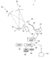
- the surface inspection apparatus of this embodiment is shown in FIG. 1, and the surface of a semiconductor wafer 10 (hereinafter referred to as wafer 10), which is a substrate, is inspected by this apparatus.
- the surface inspection apparatus 1 of the present embodiment includes a stage 5 that supports a substantially disk-shaped wafer 10, and the wafer 10 that is transferred by a transfer device (not shown) is placed on the stage 5. It is placed and fixed and held by vacuum suction.
- the stage 5 supports the wafer 10 so that the wafer 10 can rotate (rotate within the surface of the wafer 10) with the rotational axis of symmetry of the wafer 10 (the central axis of the stage 5) as the rotation axis.
- the orientation of the wafer due to this rotation will be referred to as the wafer orientation angle for convenience.
- the stage 5 can tilt (tilt) the wafer 10 about an axis (tilt axis) passing through a support surface that supports the wafer 10, and can adjust the incident angle of illumination light. Yes.
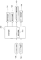
- the surface inspection apparatus 1 further includes an illumination system 20 that irradiates illumination light as parallel light on the entire surface of the wafer 10 supported by the stage 5, and reflected light from the entire surface of the wafer 10 when irradiated with illumination light.
- a light receiving system 30 that collects diffracted light and the like; an imaging device 35 that receives light collected by the light receiving system 30 and detects an image on the surface of the wafer 10; an image processing unit 40; And a storage unit 45.
- the illumination system 20 includes an illumination unit 21 that emits illumination light, and an illumination-side concave mirror 25 that reflects the illumination light emitted from the illumination unit 21 toward the surface of the wafer 10.
- the illumination unit 21 includes a light source unit 22 such as a metal halide lamp or a mercury lamp, a light control unit 23 that extracts light having a predetermined wavelength from the light from the light source unit 22 and adjusts the intensity, and a light control unit 23
- the light guide fiber 24 is configured to guide light to the illumination-side concave mirror 25 as illumination light.
- the surface inspection apparatus 1 includes a main control unit 50 and a hardware control unit 55 connected to the main control unit 50, and the main control unit 50 and the light source unit 22 are dimmed via the hardware control unit 55.
- the main controller 50 receives the digital image data from the imaging device 35 and sends it to the image processor 40.
- the data processed by the image processing unit 40 is sent to the inspection unit 42 by the main control unit 50 and inspected.
- the inspection result and digital image data are sent to the storage unit 45 by the main control unit 50 and stored therein.
- the light from the light source unit 22 passes through the light control unit 23, and illumination light having a predetermined wavelength (for example, a wavelength of 248 nm) having a predetermined intensity is emitted from the light guide fiber 24 to the illumination side concave mirror 25 and guided.
- the illumination light emitted from the optical fiber 24 to the illumination-side concave mirror 25 is converted into a parallel light beam by the illumination-side concave mirror 25 because the emission part of the light guide fiber 24 is disposed on the focal plane of the illumination-side concave mirror 25.
- the surface of the wafer 10 held on the surface is irradiated. Note that the relationship between the incident angle and the outgoing angle of the illumination light with respect to the wafer 10 can be adjusted by tilting the stage 5 about the tilt axis described above to change the mounting angle of the wafer 10.
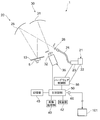
- an illumination-side polarizing filter 26 is provided between the light guide fiber 24 and the illumination-side concave mirror 25 so as to be able to be inserted into and removed from the optical path, and as shown in FIG.
- An inspection using the diffracted light (hereinafter referred to as a diffraction inspection for the sake of convenience) is performed in the extracted state, and as shown in FIG. 2, polarized light (structural complex) is inserted with the illumination side polarization filter 26 inserted in the optical path.
- An inspection using a change in polarization state due to refraction hereinafter referred to as a PER inspection for convenience) is performed (details of the illumination-side polarizing filter 26 will be described later).
- the outgoing light (diffracted light or reflected light) from the surface of the wafer 10 is collected by the light receiving system 30.
- the light receiving system 30 is mainly composed of a light receiving side concave mirror 31 disposed to face the stage 5, and emitted light (diffracted light or reflected light) collected by the light receiving side concave mirror 31 is imaged by the imaging device 35. An image of the wafer 10 is formed on the surface.
- a light receiving side polarizing filter 32 is provided between the light receiving side concave mirror 31 and the imaging device 35 so as to be inserted into and extracted from the optical path. As shown in FIG. 1, the light receiving side polarizing filter 32 is removed from the optical path. In this state, the diffraction inspection is performed, and as shown in FIG. 2, the PER inspection is performed with the light receiving side polarizing filter 32 inserted in the optical path (details of the light receiving side polarizing filter 32 will be described later). To do).
- the imaging device 35 photoelectrically converts the image of the surface of the wafer 10 formed on the imaging surface to generate an image signal (digital image data), and sends it to the main control unit 50.
- the main control unit 50 outputs the image signal to the image processing unit 40.
- the image processing unit 40 generates a digital image of the wafer 10 based on the image signal of the wafer 10 input from the imaging device 35.
- the image data of the non-defective wafer is stored in the storage unit 45 in advance, and the inspection unit 42 receives the image data of the wafer 10 and the image data of the non-defective wafer from the main control unit 50 and compares them. Inspect for defects (abnormality).
- the inspection result by the inspection unit 42 and the image of the wafer 10 at that time are output and displayed by an image display device (not shown).
- the inspection unit 42 can obtain a focus state during exposure by the exposure apparatus 101 using an image of the wafer (details will be described later).
- the illumination-side polarizing filter 26 is arranged in the illumination system 20 so that the illumination light becomes s-polarized light, and the influence of the underlayer is reduced by illuminating with the s-polarized light. Can do.
- the light-receiving side polarizing filter 32 is removed from the optical path.
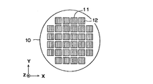
- the wafer 10 is projected and exposed with a predetermined mask pattern onto the uppermost resist film by the exposure device 101, developed by a developing device (not shown), and then a wafer cassette (not shown) by a transport device (not shown). Or it is conveyed on the stage 5 from a developing device. At this time, the wafer 10 is transferred onto the stage 5 in a state where the alignment is performed with reference to the pattern or outer edge (notch, orientation flat, etc.) of the wafer 10. As shown in FIG. 3, a plurality of chip regions 11 are arranged vertically and horizontally (in the XY directions in FIG. 3) on the surface of the wafer 10, and in each chip region 11, a line pattern or a semiconductor pattern is formed.
- a repeating pattern 12 such as a hole pattern is formed.
- One shot of exposure often includes a plurality of chip areas, but in FIG. 3, one chip is taken as one shot for easy understanding.
- the exposure apparatus 101 is the above-described step-and-scan type exposure apparatus, and is electrically connected to the signal output unit 60 of the surface inspection apparatus 1 of the present embodiment via a cable or the like.
- the exposure control can be adjusted based on the data (signal) from.
- the illumination side polarizing filter 26 and the light receiving side polarizing filter 32 are removed from the optical path as shown in FIG. Then, the wafer 10 is transferred onto the stage 5 by a transfer device (not shown). In addition, the positional information of the pattern formed on the surface of the wafer 10 is acquired by an alignment mechanism (not shown) during the transfer, and the wafer 10 is placed at a predetermined position on the stage 5 in a predetermined direction. Can do.
- the stage 5 is rotated so that the illumination direction on the surface of the wafer 10 coincides with the pattern repetition direction (in the case of a line pattern, the illumination direction is orthogonal to the line) and the pattern pitch.
- Is P ⁇ is the wavelength of the illumination light that irradiates the surface of the wafer 10
- ⁇ 1 is the incident angle of the illumination light
- ⁇ 2 is the exit angle of the n-th order diffracted light. Settings are made so that they are satisfied (tilt stage 5).
- the illumination system 20 irradiates the surface of the wafer 10 with illumination light.
- the light from the light source unit 22 in the illumination unit 21 passes through the dimming unit 23 and has a predetermined wavelength (for example, a wavelength of 248 nm).
- Intense illumination light is emitted from the light guide fiber 24 to the illumination-side concave mirror 25, and the illumination light reflected by the illumination-side concave mirror 25 is irradiated onto the surface of the wafer 10 as a parallel light beam.
- the diffracted light diffracted on the surface of the wafer 10 is collected by the light-receiving-side concave mirror 31 and reaches the image pickup surface of the image pickup device 35 to form an image (diffraction image) of the wafer 10.
- a condition of diffracted light determined by a combination of a wafer azimuth angle, an illumination wavelength, an illumination angle, an emission angle, a diffraction order, and the like is referred to as a diffraction condition.
- the imaging device 35 photoelectrically converts the image of the surface of the wafer 10 formed on the imaging surface to generate an image signal, and outputs the image signal to the image processing unit 40.
- the image processing unit 40 generates a digital image of the wafer 10 (hereinafter, the digital image of the wafer 10 based on diffracted light is referred to as a diffracted image for convenience) based on the image signal of the wafer 10 input from the imaging device 35. To do. Further, when generating the diffraction image of the wafer 10, the image processing unit 40 sends the diffraction image to the inspection unit 42 via the main control unit 50, and the inspection unit 42 outputs the image data of the wafer 10 and the image data of the non-defective wafer.
- the presence or absence of a defect (abnormality) on the surface of the wafer 10 is inspected. Then, the inspection results by the image processing unit 40 and the inspection unit 42 and the diffraction image of the wafer 10 at that time are output and displayed by an image display device (not shown).
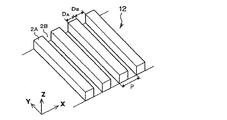
- the repeated pattern 12 is a resist pattern (line pattern) in which a plurality of line portions 2 ⁇ / b> A are arranged at a constant pitch P along the short direction (X direction). . Further, a space 2B is provided between the adjacent line portions 2A. Further, the arrangement direction (X direction) of the line portions 2A will be referred to as a “repetitive direction of the repeated pattern 12”.
- the PER inspection performs an abnormality inspection of the repetitive pattern 12 by using a change in the volume ratio between the line portion 2A and the space portion 2B in the repetitive pattern 12 as described above.
- the ideal volume ratio (design value) is 1: 1.
- the change in the volume ratio is caused by deviation from the appropriate value of the exposure focus, and appears for each shot area of the wafer 10.
- the volume ratio can also be referred to as the area ratio of the cross-sectional shape.
- the illumination side polarizing filter 26 and the light receiving side polarizing filter 32 are inserted on the optical path.
- the stage 5 tilts the wafer 10 to an inclination angle at which the regular reflection light from the wafer 10 irradiated with the illumination light can be received by the light receiving system 30, and stops at a predetermined rotational position.
- the repeating direction of the repeating pattern 12 on the wafer 10 is held so as to be inclined by about 45 degrees with respect to the vibration direction of the illumination light (linearly polarized light L) on the surface of the wafer 10.
- the repeating direction of the repeated pattern 12 on the wafer 10 is inclined by about 45 degrees with respect to the vibration direction of the illumination light (linearly polarized light L) on the surface of the wafer 10
- the light quantity for the inspection of the repeated pattern 12 can be maximized.
- the repetitive direction of the repetitive pattern 12 on the wafer 10 is about 22.5 degrees or about 67.5 with respect to the vibration direction of the illumination light (linearly polarized light L) on the surface of the wafer 10. If it is set at a degree, the sensitivity of the inspection can be increased.
- an angle is not restricted to these, It can set to an arbitrary angle direction.
- the illumination-side polarizing filter 26 is disposed between the light guide fiber 24 and the illumination-side concave mirror 25, and its transmission axis is set to a predetermined direction, and the light from the illumination unit 21 is linearly set according to the transmission axis. Extract polarized light.
- the illumination-side concave mirror 25 converts the light transmitted through the illumination-side polarizing filter 26 into a parallel light beam and is a wafer as a substrate. Illuminate 10.
- the light emitted from the light guide fiber 24 becomes p-polarized linearly polarized light L (see FIG. 5) via the illumination-side polarizing filter 26 and the illumination-side concave mirror 25, and is applied to the entire surface of the wafer 10 as illumination light. Irradiated.
- the traveling direction of the linearly polarized light L (the direction of the principal ray of the linearly polarized light L reaching an arbitrary point on the surface of the wafer 10) is substantially parallel to the optical axis.
- the linearly polarized light L incident on the wafer 10 is p-polarized light, as shown in FIG. 5, the repeating direction of the repeated pattern 12 is the incident surface of the linearly polarized light L (the traveling direction of the linearly polarized light L on the surface of the wafer 10).
- the angle formed by the vibration direction of the linearly polarized light L on the surface of the wafer 10 and the repeating direction of the repeating pattern 12 is also set to 45 degrees.
- the linearly polarized light L changes into the repeated pattern 12 so as to cross the repeated pattern 12 diagonally with the vibration direction of the linearly polarized light L on the surface of the wafer 10 inclined by 45 degrees with respect to the repeated direction of the repeated pattern 12. It will be incident.
- the specularly reflected light reflected on the surface of the wafer 10 is collected by the light receiving side concave mirror 31 of the light receiving system 30 and reaches the image pickup surface of the image pickup device 35. At this time, the light is reflected straight by the structural birefringence in the repetitive pattern 12.
- the polarization state of the polarized light L changes.
- the light receiving side polarizing filter 32 is disposed between the light receiving side concave mirror 31 and the imaging device 35, and the direction of the transmission axis of the light receiving side polarizing filter 32 is orthogonal to the transmission axis of the illumination side polarizing filter 26 described above. Is set (cross Nicole state).
- the light receiving side polarizing filter 32 allows the polarized light component (for example, the s-polarized light component) whose vibration direction is substantially perpendicular to the linearly polarized light L of the regular reflected light from the wafer 10 (repeated pattern 12) to pass through, and to capture the image pickup device. 35.
- a reflected image of the wafer 10 is formed on the imaging surface of the imaging device 35 with a polarized light component whose vibration direction is substantially perpendicular to the linearly polarized light L of the regular reflected light from the wafer 10.
- the light receiving side polarizing filter 32 can be rotated about the optical axis, and the sensitivity is improved by adjusting the minor axis direction of the elliptically polarized regular reflected light and the transmission axis of the light receiving side polarizing filter 32. Can be made. Also in this case, the adjustment angle is several degrees, which is an orthogonal category.
- the illumination side polarizing filter 26 and the light receiving side polarizing filter 32 are inserted on the optical path, and the wafer is then transferred by a not-shown transfer apparatus. 10 is conveyed onto the stage 5.
- the positional information of the pattern formed on the surface of the wafer 10 is acquired by an alignment mechanism (not shown) during the transfer, and the wafer 10 is placed at a predetermined position on the stage 5 in a predetermined direction. Can do.
- the stage 5 tilts the wafer 10 at an inclination angle at which the regular reflection light from the wafer 10 irradiated with the illumination light can be received by the light receiving system 30, stops at a predetermined rotational position, and repeats on the wafer 10.
- the repeating direction of the pattern 12 is held so as to be inclined by 45 degrees with respect to the vibration direction of the illumination light (linearly polarized light L) on the surface of the wafer 10.
- the illumination system 20 irradiates the surface of the wafer 10 with illumination light.
- the light emitted from the light guide fiber 24 of the illumination unit 21 passes through the illumination-side polarizing filter 26 and the illumination-side concave mirror 25 and is p-polarized linearly polarized light L.
- the entire surface of the wafer 10 is irradiated as illumination light.
- the specularly reflected light reflected from the surface of the wafer 10 is collected by the light-receiving-side concave mirror 31 and reaches the image pickup surface of the image pickup device 35 to form an image (reflected image) of the wafer 10.
- the polarization state of the linearly polarized light L changes due to the structural birefringence in the repeating pattern 12, and the light receiving side polarizing filter 32 causes the linearly polarized light L and the vibration direction of the regular reflected light from the wafer 10 (repeating pattern 12).
- a reflected image of the wafer 10 is formed on the imaging surface of the imaging device 35 with a polarized light component that is substantially perpendicular to the linearly polarized light L of the regular reflected light from the wafer 10.
- the imaging device 35 photoelectrically converts an image (reflected image) of the surface of the wafer 10 formed on the imaging surface to generate an image signal (digital image data), and the image signal is transmitted via the main control unit 50.
- the image is output to the image processing unit 40.
- the image processing unit 40 generates a digital image of the wafer 10 (hereinafter, the digital image of the wafer 10 based on the polarization is referred to as a polarization image for convenience) based on the image signal of the wafer 10 input from the imaging device 35. .
- the image processing unit 40 sends the polarization image to the inspection unit 42 via the main control unit 50, and the inspection unit 42 outputs the image data of the wafer 10 and the image data of the non-defective wafer.
- the presence or absence of a defect (abnormality) on the surface of the wafer 10 is inspected. Since the signal intensity (luminance value) of the reflected image of the non-defective wafer is considered to indicate the highest signal intensity (luminance value), for example, the signal intensity change (luminance change) compared to the non-defective wafer is determined in advance.
- the inspection results by the image processing unit 40 and the inspection unit 42 and the polarization image of the wafer 10 at that time are output and displayed by an image display device (not shown).
- the signal intensity is signal intensity corresponding to light detected by the imaging element of the imaging device 35, such as diffraction efficiency, intensity ratio, energy ratio, and the like.
- specular reflection inspection it is also possible to perform inspection based on specularly reflected light from the surface of the wafer 10 (hereinafter referred to as specular reflection inspection for convenience).
- specular reflection inspection the image processing unit 40 generates a digital image based on the regular reflection light from the surface of the wafer 10 (hereinafter referred to as a regular reflection image for convenience), and generates the regular reflection image of the wafer 10. Based on this, the presence or absence of defects (abnormalities) on the surface of the wafer 10 is inspected.
- the inspection unit 42 uses a wafer image that has been exposed and developed under conditions in which the focus offset amount of the exposure apparatus 101 is changed for each shot, and uses a focus curve (focus offset amount and diffracted light of the exposure apparatus 101).
- a curve indicating the relationship between signal strengths) can be obtained.
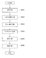
- a method for obtaining the inclination of the image plane of the mask pattern projected and exposed by the exposure apparatus 101 will be described with reference to the flowchart shown in FIG.
- a wafer on which a repeated pattern is formed by changing the focus offset amount (known) of the exposure apparatus 101 is created (step S101).
- the focus offset amount is changed for each exposure shot, a plurality of shots having the same focus offset amount are set, and the shots are arranged separately to be exposed and developed.
- a conditional wafer 10a see FIGS. 7 and 8).
- the shots having the same focus offset amount are arranged separately to cancel the influence of, for example, a difference in resist conditions generated between the center side and the outer peripheral side of the wafer and a so-called left-right difference at the time of scan exposure. Do it for the purpose.
- the resist film (photoresist) formed on the wafer is often formed by coating by spin coating, and as the resist stock solution spreads by spin, the solvent component volatilizes and the viscosity tends to increase and the film tends to become thicker.
- a difference in resist conditions occurs between the center side and the outer peripheral side of the wafer.
- the so-called left / right difference means that, for example, when the scanning direction is the X direction, the reticle moves in the X + direction (the wafer moves in the X ⁇ direction) and the reticle moves in the X ⁇ direction ( This is the difference in exposure while the wafer is moving in the X + direction.
- the condition-wafer 10a swings the focus offset amount in 16 steps from -175 nm to +200 nm in increments of 25 nm.
- Each of the shots in FIG. 7 is indicated by a number (1 to 16) of the stage of the focus offset amount that is shaken in increments of 25 nm, and “′” is attached when the stage is the same and the scanning direction is the reverse direction. is doing.
- exposure with the same focus offset amount as in the shot of the focus offset amount represented by the number 12 is performed by the reticle movement X + direction / center side, one shot / reticle movement X + direction / outer periphery side, one shot / reticle movement X.
- X-Four positions can be set like one shot in the-direction / outer periphery side. Further, for example, exposure with the same focus offset amount as in the shot of the focus offset amount represented by number 15 is performed by two shots / reticle movement in the reticle movement X + direction / outer peripheral side with the center of the conditionally adjusted wafer 10a as the axis of symmetry. Four positions can be set like 2 shots in the X-direction / outer peripheral side. In the example of FIG. 7, the focus offset amount is 16 stages, and each focus offset amount is a total of 64 shots, for a total of 64 shots.
- a plurality of conditioned wafers may be made to obtain the focus curve.
- the shot arrangement for each focus offset amount of each conditionally adjusted wafer is set so as to cancel the influence due to conditions other than the focus offset.
- the conditioned wafer 10a is transferred onto the stage 5 in the same manner as in the diffraction inspection (step S102).
- the illumination system 20 irradiates illumination light onto the surface of the conditioned wafer 10a, and the imaging device 35 photoelectrically converts the diffracted image of the conditioned wafer 10a to generate an image signal,
- the image signal is output to the image processing unit 40 (step S103).
- the diffraction conditions are obtained by using the information of the exposed mask pattern or the diffraction condition search, and the same setting as in the diffraction inspection is performed so that diffracted light is obtained.
- the tilt angle of the stage 5 is changed stepwise in an angle range other than specular reflection to acquire images at the respective tilt angles, and the image is brightened, that is, the tilt angle at which diffracted light is obtained is obtained. Refers to the function.
- the image processing unit 40 generates a diffracted image of the conditionally adjusted wafer 10a based on the image signal of the conditionally adjusted wafer 10a input from the imaging device 35, and performs a pixel unit for each shot with the same focus offset amount (respectively).
- the signal intensities are averaged between the corresponding pixels of the shots (step S104). Note that a portion determined to be a defect by the diffraction inspection is excluded from the above-described averaging target.
- the image processing unit 40 surrounds all shots obtained by averaging (that is, different focus offset amounts) with a plurality of setting areas (small rectangles) set in the shot as shown in FIG.
- the average values of the signal intensities A) (hereinafter referred to as average luminance for convenience) are respectively obtained (step S105). With the processing so far, the average luminance is obtained for each of the plurality of setting areas A provided in the exposure shot when the focus offset is changed in 16 steps from -175 nm to +200 nm in increments of 25 nm.
- the image processing unit 40 sends the averaged data to the inspection unit 42 via the main control unit 50, and the inspection unit 42, as shown in FIG. ,
- a graph showing the relationship between the average luminance in the setting area A at the same position in each shot (with different focus offset amounts) and the corresponding focus offset amount, that is, a focus curve is obtained (step S106).
- the inspection unit 42 obtains approximate curves of the focus curve, respectively (step S107).
- the focus curve obtained here is appropriately referred to as a reference focus curve.
- other arbitrary function forms for example, a cubic expression, etc.
- the inspection unit 42 obtains a focus offset amount at which the average luminance is maximum in the approximate curve of the focus curve (that is, the maximum focus offset amount is in the range of ⁇ 175 nm to +200 nm) (step S108).
- the focus offset amount at which the average luminance is maximized is 2.5 nm.
- the focus offset amount at which the average luminance is maximized is ⁇ 14.5 nm.
- a focus offset amount that maximizes the average luminance is obtained for each setting area A (step S109). In this way, as shown in FIG. 11, it is possible to obtain the distribution of the focus offset amount that maximizes the average brightness of the diffracted light in the shot.
- the inclination of the focus offset amount in the long side direction of the slit (light) exposed by the exposure apparatus 101 that is, the image) Surface inclination
- the inclination of the focus offset amount in the scanning direction of the reticle stage and wafer stage of the exposure apparatus 101 can be obtained (approximately), respectively.
- the inclination of the image plane is a relative positional relationship between the respective image forming points, the inclination of the image plane can be obtained by obtaining the maximum value of the average luminance.
- the image plane inclination obtained in this way is converted into a parameter that can be accepted by the exposure apparatus 101, such as the curvature of field, maximum / minimum value, or diagonal inclination, and then output from the main controller 50 as a signal output.
- the data is output to the exposure apparatus 101 via the unit 60 and reflected in the exposure by the exposure apparatus 101.
- the image plane inclination in the present embodiment is the total image plane with respect to the photoresist layer on the wafer due to the image plane inclination of the projection image by the projection lens in the exposure apparatus 101 and the running error of the reticle stage and wafer stage. It is a slope.
- the inspection unit 42 also has a determination function.
- the inspection unit 42 obtains the focus state at the time of exposure by the exposure apparatus 101, more specifically, the fluctuation state of the focus of the exposure apparatus 101 with respect to the entire surface of the wafer 10, from the diffraction image of the wafer 10 to be inspected. Be able to.
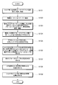
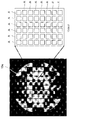
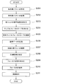
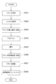
- a method for obtaining the focus state during exposure by the exposure apparatus 101 will be described with reference to the flowchart shown in FIG. First, a conditioned wafer 10b (see FIG. 13) in which a repetitive pattern is formed by changing the focus offset amount and the dose amount (exposure amount) of the exposure apparatus 101 in a matrix is created (step S201).
- the exposure shot at the center of the conditioned wafer 10b is set to the best focus and the best dose, the focus offset amount is changed for each exposure shot arranged in the horizontal direction, and the dose amount is changed for each exposure shot arranged in the vertical direction. To expose and develop.
- a diffraction image of the conditioned wafer 10b is captured and acquired (step S202).
- the conditioned wafer 10b is first transported onto the stage 5 as in the case of diffraction inspection.
- the illumination system 20 irradiates illumination light onto the surface of the conditioned wafer 10b, and the imaging device 35 photoelectrically converts the diffraction image of the conditioned wafer 10b to generate an image signal, and the image signal is sent to the image processing unit 40. Output.
- the image processing unit 40 generates a diffraction image of the conditioned wafer 10b based on the image signal of the conditioned wafer 10b input from the imaging device 35.
- the diffraction images of the conditionally adjusted wafer 10b are captured and acquired for a plurality of conditions determined by a combination of the azimuth angle, illumination wavelength, incident angle, and emission angle of the wafer, that is, for a plurality of diffraction conditions.
- the repetitive pattern of the conditioned wafer 10b has a base layer or base unevenness
- use of illumination light with a short wavelength for example, 248 nm, 313 nm, etc.
- a short wavelength for example, 248 nm, 313 nm, etc.
- the illumination side polarizing filter 26 with the transmission axis set in a predetermined direction is inserted on the optical path so that s-polarized light can be obtained as illumination light, it can be made less susceptible to the influence of the ground.
- the light-receiving side polarizing filter 32 having the transmission axis set in a predetermined direction so as to receive only diffracted light by s-polarized light is inserted on the optical path, it is possible to make it less susceptible to the influence of the ground.
- the image processing unit 40 obtains the signal intensity of each shot for each diffraction image captured and acquired under a plurality of diffraction conditions (step S203). At this time, the average signal intensity in the same shot is defined as the signal intensity of each shot. Thereby, the influence of the inclination of the image plane can be removed.
- the image processing unit 40 sends the averaged diffraction image to the inspection unit 42 via the main control unit 50, and the inspection unit 42 obtains each of the diffraction images captured and acquired under a plurality of diffraction conditions for each different dose amount.
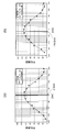
- a graph showing the relationship between the signal intensity of each shot (with the same dose amount and different focus offset amount) and the corresponding focus offset amount, that is, a focus curve (obtained when measuring the inclination of the image plane) In order to distinguish it from the reference focus curve, it is hereinafter referred to as a sample focus curve as appropriate) (step S204).
- a plurality of sample focus curves respectively corresponding to a plurality of diffraction conditions can be obtained for each different dose amount.
- the inspection unit 42 selects at least two types of sample focus curves used for obtaining the focus state at the time of exposure from a plurality of sample focus curves (step S205).
- three types of sample focus curves hereinafter referred to as reference sample focus curves as appropriate to distinguish them from other sample focus curves
- reference sample focus curves as appropriate to distinguish them from other sample focus curves
- a plurality of sample focus curves that are sensitive to changes in focus are extracted from the plurality of sample focus curves.
- a plurality of sample focus curves that are less sensitive to changes in dose are extracted from sample focus curves that are sensitive to changes in focus.
- sample focus curves that are sensitive to changes in focus and less sensitive to changes in dose
- three types of sample focus curves with different peak or bottom positions are used as reference sample focus. Select and determine as a curve.
- the sample focus curve has a plurality of sample focus curves with different doses for each of the three types of diffraction conditions, but in the subsequent calculations, the same dose amount as when the wafer whose focus state is to be measured was exposed. Or use the closest dose amount.
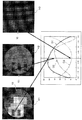
- FIG. 13 shows a diffraction image G1 from which a first reference sample focus curve D1 is obtained, a diffraction image G2 from which a second reference sample focus curve D2 is obtained, and a third reference sample focus, along with three types of reference sample focus curves D1 to D3.
- the diffraction images G3 from which the curve D3 is obtained are respectively shown. Note that each of the diffraction images G1 to G3 shown in FIG.
- each diffraction image may be captured and acquired by changing only the order of the diffracted light.
- the image processing unit 40 When the three types of reference sample focus curves are selected and determined, the image processing unit 40 outputs and stores the data related to the approximate curve equation of the determined reference sample focus curve in the storage unit 45 as reference data (step S206).
- the image processing unit 40 outputs a data map indicating the relationship between the focus offset amount obtained from the approximate curve equation and the signal intensity to the storage unit 45 as reference data, not limited to the approximate curve equation of the reference sample focus curve. And may be stored.
- the NA number of aperture
- the reference data is obtained for each illumination condition and stored in the storage unit 45.
- a diffraction image of the wafer 10 to be inspected is captured and acquired (step S207). At this time, a diffraction image of the wafer 10 is captured and acquired for each of the same three types of diffraction conditions as the diffraction image from which the reference sample focus curve is obtained.
- the image processing unit 40 determines from the signal intensity for each pixel of the diffraction image whether the region corresponding to each pixel is a measurement region in the shot (step S208). ), Pixels corresponding to streets and the like are excluded from the measurement target.
- the image processing unit 40 sends the diffraction image to the inspection unit 42 via the main control unit 50, and the inspection unit 42 inspects the wafer 10 to be inspected.
- the focus fluctuation state of the exposure apparatus 101 with respect to the surface of the wafer 10 is obtained (step S209).
- the exposure apparatus for the surface of the wafer 10 from the signal intensity of the diffraction image of the wafer 10 A focus offset amount 101 is obtained for each predetermined pixel (in units of one or more pixels).
- the area for obtaining the focus offset amount be an area smaller than one shot (for example, 1/10).
- the storage unit 45 stores approximate curve formulas (or data maps) of the reference sample focus curve respectively corresponding to the three types of diffraction conditions. From the signal intensity of the diffraction image of the wafer 10, the focus offset amount can be obtained for each predetermined pixel. Since the focus curve is a curve, a plurality of focus offset amount candidates may be calculated from the signal intensity of one diffraction image (only one candidate may be calculated depending on conditions). On the other hand, by using three types of reference sample focus curves D1 to D3 having different peak or bottom positions (focus offset amounts), one calculated focus offset amount is obtained as shown in FIG. It is decided.
- the focus offset amount that minimizes the sum of squared differences between the signal intensity under each diffraction condition and the approximate curve corresponding to this condition is obtained.
- three types of reference sample focus curves D1 to D3 are prepared for each different dose amount for each of the three types of diffraction conditions, and a focus offset amount at a dose amount that minimizes the sum of squared differences is employed. You may do it.
- the signal intensity may be weighted under the condition that the slope of the curve is relatively large (that is, the sensitivity to the focus change is relatively high).
- the result may not be adopted as an abnormal value.
- the focus offset amount can be calculated for each pixel on the entire surface of the wafer 10, and the focus fluctuation state of the exposure apparatus 101 with respect to the surface of the wafer 10 can be determined.
- the diffraction image H1 and the second reference sample focus curve D2 of the wafer 10 imaged under the diffraction conditions for obtaining the first reference sample focus curve D1 are obtained together with the three types of reference sample focus curves D1 to D3.
- a diffraction image H2 of the wafer 10 imaged under the diffraction condition and a diffraction image H3 of the wafer 10 imaged under the diffraction condition for obtaining the third reference sample focus curve D3 are shown.
- the degree of coincidence with the first reference sample focus curve D1), the second detection signal (second signal intensity K2) corresponding to the diffracted light based on the second diffraction condition from the repeated pattern 12, and the second reference data corresponding to the diffraction condition ( The degree of coincidence with the second reference sample focus curve D2), the third detection signal (third signal intensity K3) corresponding to the diffracted light from the repetitive pattern 12 under the third diffraction condition, and the third corresponding to this diffraction condition It can be seen that the degree of coincidence with the reference data (third reference sample focus curve D3) is high.
- the inspection unit 42 inspects whether the obtained focus offset amount is abnormal (step S210). At this time, for example, if the obtained focus offset amount is within a predetermined threshold range, the inspection unit 42 determines that the normal state is normal, and if the obtained focus offset amount is out of the predetermined threshold range, an abnormality occurs. Is determined.
- the storage unit may be prepared outside the surface inspection apparatus 1 (for example, a control room of a semiconductor manufacturing line) and read out an approximate curve formula (or data map) of the reference sample focus curve through the line. it can.
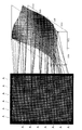
- the image processing unit 40 When the presence / absence of the focus offset amount is inspected, the image processing unit 40 generates an image of the wafer 10 in which the focus offset amount obtained for each pixel is converted into the signal intensity at the pixel, and the focus offset amount inspection result is obtained. And the like are displayed on an image display device (not shown) (step S211).
- the image display device is not limited to the surface inspection device 1 of the present embodiment, and an image display device provided and connected to the outside of the inspection device (for example, a management room of a semiconductor production line) may be used.
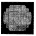
- FIG. 16 shows an example of an image of the wafer 10 obtained by converting the focus offset amount into the signal intensity. Note that the image shown in FIG. 16 is not limited to a black and white image, and may be displayed as a color image.
- the inspection unit 42 includes the first detection signal (first signal intensity K1) detected by the imaging device 35 and the first reference data (first reference sample focus).
- the degree of coincidence between the third reference data (third reference sample focus curve D3) and the focus state (processing condition) at the time of exposure for the repetitive pattern 12 on the wafer 10 is determined.
- the focus state at the time of exposure can be calculated
- reference sample focus curves D1 to D3 Three types of reference data (reference sample focus curves D1 to D3) that are sensitive to changes in focus and less sensitive to changes in dose (exposure amount) are used, and the sensitivity (detection signal) to changes in focus Change) is greater than the sensitivity to the change in dose (change in detection signal). Therefore, it is possible to eliminate the influence due to the change in the dose amount, and it is possible to measure the focus state at the time of exposure more accurately.
- the stage 5 can be tilted around a tilt axis that passes through a support surface that supports the wafer 10, that is, rotates about an axis that is substantially parallel to the supported surface of the wafer 10 and substantially orthogonal to the direction in which illumination light travels. It is configured to be movable.
- the diffraction conditions incident angle of illumination light, etc.
- the focus state during exposure can be changed. It can be measured in a shorter time.
- three types of reference data are used to determine the focus state (processing conditions) at the time of exposure for the repetitive pattern 12 on the wafer 10.
- two types of reference data or five types of reference data may be used.
- the focus state at the time of exposure can be determined using at least two types of reference data that differ in how the detection signal changes with respect to the change in focus.
- the inspection of the repeated pattern 12 exposed and formed on the resist film on the wafer 10 is performed.
- the present invention is not limited to this, and the pattern after etching may be inspected. Good. Thereby, not only the focus state at the time of exposure but also a defect (abnormality) at the time of etching can be detected.
- the polarization image (PER image) of the conditioned wafer 10b is used for each different dose amount in the same manner as described above.
- a plurality of sample focus curves based on the polarization determined by the azimuth angle and the illumination wavelength may be obtained, and a plurality of reference sample focus curves based on the polarization may be selected and determined from these.
- the reference sample focus curve (reference data) based on the polarization the fluctuation state of the focus of the exposure apparatus 101 with respect to the surface of the wafer 10 is obtained from the signal intensity of the polarization image captured and acquired by the imaging apparatus 35.
- the focus state at the time of exposure can be measured with higher accuracy. Further, in measurement using polarized light, the focus offset amount at which the signal intensity is maximized in the focus curve is considered as the best focus, so that the focus offset amount that is the best focus can be easily known.
- the diffraction image and the polarization image may be used in combination such that the first detection signal is a diffraction image and the second detection signal is a polarization image.
- the repetitive pattern 12 on the wafer 10 is used by using three types of reference data (reference sample focus curves D1 to D3) that are sensitive to a change in focus and less sensitive to a change in dose.
- the focus state at the time of exposure is determined, but by extracting multiple sample focus curves from multiple sample focus curves that are sensitive to changes in dose and less sensitive to changes in focus,
- the dose amount at the time of exposure of the repetitive pattern 12 on the wafer 10 can also be determined using the sample dose curve obtained by replacing the focus of the sample focus curve with the dose.
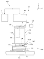
- the exposure system 100 includes an exposure apparatus 101 that projects and exposes a predetermined mask pattern (repeated pattern) on the surface of a wafer 10 coated with a resist, an exposure process by the exposure apparatus 101, and a development process by a developing apparatus (not shown). And the like, and a surface inspection apparatus 1 for inspecting the wafer 10 having the repeated pattern 12 formed on the surface.
- the exposure apparatus 101 includes an illumination system 110, a reticle stage 120, a projection unit 130, a local immersion apparatus 140, a stage apparatus 150, and a main controller 200 (see FIG. 18). It is configured with.
- the directions of arrows X, Y, and Z shown in FIG. 17 will be described as the X-axis direction, the Y-axis direction, and the Z-axis direction, respectively.
- the illumination system 110 includes a light source, an illuminance equalizing optical system including an optical integrator, and an illumination optical system including a reticle blind.
- the reticle is defined by the reticle blind.
- the slit-shaped illumination area on R is illuminated with illumination light (exposure light) with substantially uniform illuminance.
- illumination light for example, ArF excimer laser light (wavelength 193 nm) is used.
- a reticle (photomask) R having a predetermined pattern (for example, a line pattern) formed on the pattern surface (the lower surface in FIG. 17) is fixedly held by, for example, vacuum suction.
- the reticle stage 120 can be moved in the XY plane by a reticle stage driving device 121 (see FIG. 18) including a linear motor, for example, and at a predetermined scanning speed in the scanning direction (here, the Y-axis direction). It is configured to be movable.
- Position information of the reticle stage 120 in the XY plane (including rotation information about the rotation direction around the Z axis) is reflected on the first reflecting mirror 123 having a reflecting surface orthogonal to the Y axis provided on the reticle stage 120 and the X axis.
- Detection is performed by the reticle interferometer 125 via a second reflecting mirror (not shown) having an orthogonal reflecting surface.
- the position information detected by the reticle interferometer 125 is sent to the main controller 200, and the main controller 200 moves the position (and moving speed) of the reticle stage 120 via the reticle stage driving device 121 based on the position information. To control.
- the projection unit 130 is disposed below the reticle stage 120 and includes a lens barrel 131 and a projection optical system 135 held in the lens barrel 131.
- the projection optical system 135 has a plurality of optical elements (lens elements) arranged along the optical axis AX of illumination light, is telecentric on both sides, and has a predetermined projection magnification (for example, 1/4 times, 1/5 times or 1/8 times, etc.). For this reason, when the illumination area on the reticle R is illuminated by the illumination light emitted from the illumination system 110, the illumination light transmitted through the reticle R arranged so that the object plane and the pattern plane of the projection optical system 135 substantially coincide with each other.
- a reduced image of the pattern of the reticle R in the illumination area via the projection optical system 135 is conjugated to the exposure area on the wafer 10 arranged on the image plane side of the projection optical system 135 (the illumination area on the reticle R).
- a region The reticle R is moved in the scanning direction (Y-axis direction) with respect to the illumination area by the synchronous driving of the reticle stage 120 and the stage apparatus 150 that holds the wafer 10, and the wafer 10 is moved in the scanning direction with respect to the exposure area.
- scanning exposure of one shot area on the wafer 10 is performed, and the pattern (mask pattern) of the reticle R is transferred to the shot area.
- the exposure apparatus 101 is provided with a local immersion apparatus 140 for performing immersion type exposure.
- the local liquid immersion device 140 includes a liquid supply device 141, a liquid recovery device 142, a liquid supply tube 143A, a liquid recovery tube 143B, and a nozzle unit 145. Is done.
- the nozzle unit 145 holds the projection unit 130 so as to surround the periphery of the lower end portion of the lens barrel 131 that holds the optical element on the most image plane side (wafer side) constituting the projection optical system 135, here the tip lens 136. It is supported by a frame member (not shown) (a frame member constituting the exposure apparatus 101). Further, as shown in FIG. 17, the nozzle unit 145 is set so that its lower end surface is substantially flush with the lower end surface of the front lens 136.
- the liquid supply device 141 includes a tank that stores liquid, a pressurizing pump, a temperature control device, and a valve that controls the flow rate of the liquid. It is connected to the nozzle unit 145 via a pipe 143A.
- the liquid recovery apparatus 142 includes a tank for storing the recovered liquid, a suction pump, and a valve for controlling the flow rate of the liquid, and is provided via a liquid recovery pipe 143B. Are connected to the nozzle unit 145.
- the main control device 200 controls the operation of the liquid supply device 141 to supply liquid (for example, pure water) between the tip lens 136 and the wafer 10 via the liquid supply tube 143A.
- the operation of the liquid recovery device 142 is controlled to recover the liquid from between the front lens 136 and the wafer 10 via the liquid recovery tube 143B.
- the main controller 200 controls the operation of the liquid supply device 141 and the liquid recovery device 142 so that the amount of supplied liquid and the amount of recovered liquid are always equal. Therefore, a fixed amount of liquid is always exchanged and held between the front lens 136 and the wafer 10, thereby forming an immersion area (immersion space).
- the wafer 10 is exposed by irradiating the wafer 10 with illumination light through the liquid forming the liquid immersion area.
- the stage device 150 includes a wafer stage 151 disposed below the projection unit 130, and a stage driving device 155 (see FIG. 18) for driving the wafer stage 151.
- Wafer stage 151 has a clearance of about several ⁇ m by an air slider (not shown) and is supported to float above base member 105, and is configured to hold wafer 10 on the upper surface of wafer stage 151 by vacuum suction. .
- the wafer stage 151 can be moved in the XY plane along the upper surface of the base member 105 by a motor constituting the stage driving device 155.
- the position information of the wafer stage 151 in the XY plane is detected by the encoder device 156 (see FIG. 18).
- the position information detected by the encoder device 156 is sent to the main control device 200, and the main control device 200 controls the position (and moving speed) of the wafer stage 151 via the stage driving device 155 based on the position information. To do.
- the object plane and the pattern plane of the projection optical system 135 are substantially aligned.
- the reduced image of the pattern of the reticle R in the illumination area is supported on the wafer stage 151 and arranged on the image plane side of the projection optical system 135 through the projection optical system 135 by the illumination light transmitted through the reticle R. Is formed in an exposed region on the wafer 10 (region conjugate to the illumination region on the reticle R).
- the reticle R is moved in the scanning direction (Y-axis direction) with respect to the illumination area, and the wafer 10 is moved in the scanning direction with respect to the exposure area.
- scanning exposure of one shot area on the wafer 10 is performed, and the pattern of the reticle R is transferred to the shot area.
- the pattern 12 is repeatedly formed on the surface by the surface inspection apparatus 1 according to the above-described embodiment after the development process by the development apparatus (not shown).
- the surface of the wafer 10 is inspected.
- the inspection unit 42 of the surface inspection apparatus 1 obtains the fluctuation state of the focus of the exposure apparatus 101 with respect to the surface of the wafer 10 as described above, and the signal output unit 60 and the connection cable (see FIG.
- the information about the obtained focus fluctuation state (focus offset amount) is output to the exposure apparatus 101 via a not-shown).
- the correction processing unit 210 provided in the main controller 200 of the exposure apparatus 101 focuses the exposure apparatus 101 on the surface of the wafer 10 based on the focus fluctuation state of the exposure apparatus 101 input from the surface inspection apparatus 1.
- Various setting parameters related to the focus of the exposure apparatus 101 and the arrangement state of the optical elements are corrected so that the state becomes constant.
- the exposure setting is corrected in order to correct the focus setting of the exposure apparatus 101 according to the focus state at the time of exposure input from the surface inspection apparatus 1 according to the above-described embodiment. Since the focus state at the time can be accurately measured in a short time, correction based on the focus state with higher accuracy can be performed, and the focus of the exposure apparatus 101 can be set more appropriately.
- a semiconductor device includes a design process (step S301) for designing the function and performance of the device, a reticle production process (step S302) for producing a reticle based on the design process, and a wafer for producing a wafer from a silicon material.
- Manufacturing process step S303), reticle pattern transferred to wafer by exposure or the like (including exposure process, development process, etc.) lithography process (step S304), device assembly (dicing process, bonding process, package process, etc.) And an assembly process (step S305), an inspection process for inspecting a device (step S306), and the like.
- a wafer is prepared (step S401), and a resist is applied to the wafer surface to have a predetermined thickness using a coating apparatus such as a spin coater (not shown) (step S402).
- a coating apparatus such as a spin coater (not shown)
- the solvent component of the resist is evaporated by a drying device in the coating device, and film formation is performed on the coated wafer.
- the wafer on which the resist is formed is transferred to the exposure apparatus 101 by a transfer device (not shown) (step S403).
- the wafer carried into the exposure apparatus 101 is aligned by the alignment apparatus provided in the exposure apparatus 101 (step S404).
- the reticle pattern is subjected to reduced exposure on the aligned wafer (step S405).
- the exposed wafer is transferred from the exposure apparatus 101 to a developing device (not shown) and developed (step S406).
- the developed wafer is set by the surface inspection apparatus 1, the focus state of the exposure apparatus 101 is obtained as described above, and the pattern produced on the wafer is inspected by performing diffraction inspection and polarization inspection (S407).
- a wafer in which a defect (abnormality) occurs more than a reference predetermined in the inspection is sent to rework (regeneration processing), and a wafer in which the defect (abnormality) is less than the reference is subjected to post-processing such as an etching process.
- the focus state of the exposure apparatus 101 obtained in step S407 is fed back to the exposure apparatus 101 for correction of focus setting (step S408).
- pattern exposure is performed using the exposure system 100 according to the above-described embodiment in a lithography process. That is, as described above, when the exposure process by the exposure apparatus 101 is performed, the wafer 10 on which the repeated pattern 12 is formed on the surface by the surface inspection apparatus 1 after the development process by the developing apparatus (not shown) and the like. Perform surface inspection. At this time, the surface inspection apparatus 1 determines the focus state at the time of exposure, and the exposure apparatus 101 corrects the focus setting of the exposure apparatus 101 according to the focus state at the time of exposure input from the surface inspection apparatus 1. . As described above, according to the semiconductor device manufacturing method of the present embodiment, the focus state at the time of exposure can be accurately measured in a short time, so that the focus of the exposure apparatus 101 can be set more appropriately. Highly integrated semiconductor devices can be manufactured with high productivity.
- the immersion type exposure apparatus 101 provided with the local immersion apparatus 140 has been described as an example of the exposure apparatus.
- the present teaching is not limited to this, and the exposure system according to the present teaching and The semiconductor device manufacturing method can also be applied to an exposure apparatus that is not an immersion type exposure apparatus.
- the present invention can be applied to an inspection apparatus used in an inspection process after development in the manufacture of a semiconductor device. Thereby, the inspection accuracy of the inspection apparatus can be improved, and the manufacturing efficiency of the semiconductor device can be improved.
Landscapes
- Physics & Mathematics (AREA)
- General Physics & Mathematics (AREA)
- Immunology (AREA)
- Pathology (AREA)
- Chemical & Material Sciences (AREA)
- Analytical Chemistry (AREA)
- Biochemistry (AREA)
- General Health & Medical Sciences (AREA)
- Health & Medical Sciences (AREA)
- Life Sciences & Earth Sciences (AREA)
- Optics & Photonics (AREA)
- Investigating Materials By The Use Of Optical Means Adapted For Particular Applications (AREA)
- Exposure And Positioning Against Photoresist Photosensitive Materials (AREA)
- Exposure Of Semiconductors, Excluding Electron Or Ion Beam Exposure (AREA)
- Testing Or Measuring Of Semiconductors Or The Like (AREA)
- Length Measuring Devices By Optical Means (AREA)
Abstract
Description

10 ウェハ(10a,10b 条件振りウェハ)
20 照明系
30 受光系(検出部) 35 撮像装置(検出部)
40 画像処理部 42 検査部(判定部)
45 記憶部 50 主制御部
100 露光システム 101 露光装置
Claims (21)
- 所定の加工条件で加工されたパターンを有する基板の表面の所定領域を照明光で照明する照明部と、
前記所定領域内にあるパターンから第1方向に進む第1の光に応じた第1検出信号と、前記第1方向と異なる第2方向に進む第2の光に応じた第2検出信号とを検出する検出部と、
複数の既知の加工条件で加工された複数のパターンを有する少なくとも1つの基板に対して、前記検出部により検出される第1検出信号と前記既知の複数の加工条件の関係を示す第1基準データと、前記検出部により検出される第2検出信号と前記既知の複数の加工条件の関係を示す第2基準データとを準備する準備部と、
加工条件を求めるべき基板に対して前記検出部によって検出される第1検出信号と前記第1基準データとの一致度と、前記基板に対して前記検出部によって検出される第2検出信号と前記第2基準データとの一致度とに基づいて前記基板上のパターンの加工条件を判定する判定部とを有することを特徴とする表面検査装置。 - 前記パターンは前記所定領域毎の露光により設けられるパターンであり、前記判定部で求められる前記加工条件は、前記露光時のフォーカス状態と露光量の少なくとも一方であり、
前記加工条件の変化に対する前記第1検出信号の変化と、前記加工条件の変化に対する前記第2検出信号の変化とが相反することを特徴とする請求項1に記載の表面検査装置。 - 前記判定部で判定される前記加工条件は前記フォーカス状態であり、前記フォーカス状態の変化に対する前記第1検出信号及び第2検出信号の変化は、前記露光量の変化に対する変化よりも大きいことを特徴とする請求項2に記載の表面検査装置。
- 前記準備部は、前記第1基準データと前記第2基準データを記憶する記憶部であることを特徴とする請求項1から3のいずれか一項に記載の表面検査装置。
- 前記第1検出信号と前記第2検出信号の少なくとも一方は、回折光に基づくことを特徴とする請求項1から4のいずれか一項に記載の表面検査装置。
- 前記第1方向と前記第2方向は、前記所定領域内にあるパターンで発生する異なる次数の回折光の進む方向であることを特徴とする請求項5に記載の表面検査装置。
- 前記第1検出信号と前記第2検出信号の少なくとも一方は、所定の偏光成分に基づくことを特徴とする請求項1から4のいずれか一項に記載の表面検査装置。
- 前記検出部は前記第1方向とも前記第2方向とも異なる第3方向に進む第3の光に応じた第3検出信号を検出可能であり、
前記準備部には、前記複数のパターンを有する基板に対して、前記検出部により検出される第3検出信号と前記既知の複数の加工条件の関係を示す第3基準データがさらに記憶されており、
前記判定部は、前記被検基板に対して前記検出部によって検出される第1検出信号と前記第1基準データとの一致度と、前記被検基板に対して前記検出部によって検出される第2検出信号と前記第2基準データとの一致度と、前記被検基板に対して前記検出部によって検出される第3検出信号と前記第3基準データとの一致度とに基づいて前記被検基板上のパターンの加工条件を判定することを特徴とする請求項1から7のいずれか一項に記載の表面検査装置。 - 前記基板を支持するステージをさらに有し、該ステージが前記基板の前記支持された面と略平行で前記照明光の進む方向に略直交する軸を中心に回動可能であることを特徴とする請求項1から8のいずれか一項に記載の表面検査装置。
- 前記検出部は、前記基板を照明する照明光の光路に挿抜自在に設けられ、前記照明光のうちs偏光成分を透過させるように構成された照明側偏光フィルタ、又は、第1又は第2の光路に挿抜自在に設けられ、前記第1、第2の光のうちs偏光成分を透過させるように構成された受光側偏光フィルタを備える請求項1から8のいずれか一項に記載の表面検査装置。
- 基板の表面に所定のパターンを露光する露光装置と、前記露光装置により露光されて表面に前記パターンが設けられた基板の表面検査を行う表面検査装置とを備え、
前記表面検査装置は、請求項1から10のいずれか一項に記載の表面検査装置であって、前記判定部で求められた前記加工条件として前記露光時のフォーカス状態を前記露光装置へ出力し、
前記露光装置は、前記表面検査装置から入力された前記露光時のフォーカス状態に応じて、前記露光装置のフォーカスの設定を補正することを特徴とする露光システム。 - 前記露光装置は、前記基板に対して液体を介して前記所定のパターンを露光する液浸型の露光装置である請求項11に記載の露光システム。
- 所定の加工条件で加工されたパターンを有する基板の表面の所定領域を照明光で照明し、前記所定領域内にあるパターンから第1方向に進む第1の光に応じた第1検出信号と、前記第1方向と異なる第2方向に進む第2の光に応じた第2検出信号とを検出し、
複数の既知の加工条件で加工された複数のパターンを有する少なくとも1つの基板に対して、前記第1検出信号と前記既知の複数の加工条件の関係を示す第1基準データと、前記第2検出信号と前記既知の複数の加工条件の関係を示す第2基準データとを準備し、
加工条件を求めるべき基板から検出される第1検出信号と前記第1基準データとの一致度と、前記基板から検出される第2検出信号と前記第2基準データとの一致度とに基づいて前記基板上のパターンの加工条件を判定することを特徴とする表面検査方法。 - 前記パターンは前記所定領域毎の露光により設けられるパターンであり、前記判定される前記加工条件は、前記露光時のフォーカス状態と露光量の少なくとも一方であり、
前記加工条件の変化に対する前記第1検出信号の変化と、前記加工条件の変化に対する前記第2検出信号の変化とが相反することを特徴とする請求項13に記載の表面検査方法。 - 前記判定される前記加工条件は前記フォーカス状態であり、前記フォーカス状態の変化に対する前記第1検出信号及び第2検出信号の変化は、前記露光量の変化に対する変化よりも大きいことを特徴とする請求項14に記載の表面検査方法。
- 前記第1基準データと前記第2基準データとを記憶し、該記憶された前記第1基準データと前記第2基準データとを呼び出すことにより前記準備を行うことを特徴とする請求項13から15のいずれか一項に記載の表面検査方法。
- 前記第1検出信号と前記第2検出信号の少なくとも一方は、回折光に基づくことを特徴とする請求項13から16の何れか一項に記載の表面検査方法。
- 前記第1方向と前記第2方向は、前記所定領域内にあるパターンで発生する異なる次数の回折光の進む方向であることを特徴とする請求項17に記載の表面方法。
- 前記第1検出信号と前記第2検出信号の少なくとも一方は、所定の偏光成分に基づくことを特徴とする請求項13から16のいずれか一項に記載の表面検査方法。
- 前記第1方向とも前記第2方向とも異なる第3方向に進む第3の光に応じた第3検出信号を検出可能であり、
前記複数のパターンを有する基板に対して、前記第3検出信号と前記既知の複数の加工条件の関係を示す第3基準データをさらに記憶し、
前記被検基板から検出される第1検出信号と前記第1基準データとの一致度と、前記被検基板から検出される第2検出信号と前記第2基準データとの一致度と、前記被検基板から検出される第3検出信号と前記第3基準データとの一致度とに基づいて前記被検基板上のパターンの加工条件を判定することを特徴とする請求項13から19のいずれか一項に記載の表面検査方法。 - 基板の表面に所定のパターンを露光するリソグラフィー工程を有した半導体デバイス製造方法であって、
前記露光の後に請求項13から20のいずれか一項に記載の表面検査方法を用いて前記基板の検査を行うことを特徴とする半導体デバイス製造方法。
Priority Applications (3)
| Application Number | Priority Date | Filing Date | Title |
|---|---|---|---|
| CN201180059328.5A CN103250232B (zh) | 2010-12-14 | 2011-12-14 | 表面检查装置及其方法 |
| KR1020137015255A KR101950523B1 (ko) | 2010-12-14 | 2011-12-14 | 표면 검사 장치 및 그 방법 |
| JP2012548813A JP5867412B2 (ja) | 2010-12-14 | 2011-12-14 | 表面検査装置及びその方法 |
Applications Claiming Priority (4)
| Application Number | Priority Date | Filing Date | Title |
|---|---|---|---|
| JP2010-278308 | 2010-12-14 | ||
| JP2010278308 | 2010-12-14 | ||
| JP2011004306 | 2011-01-12 | ||
| JP2011-004306 | 2011-01-12 |
Publications (1)
| Publication Number | Publication Date |
|---|---|
| WO2012081623A1 true WO2012081623A1 (ja) | 2012-06-21 |
Family
ID=46234906
Family Applications (2)
| Application Number | Title | Priority Date | Filing Date |
|---|---|---|---|
| PCT/JP2011/078819 Ceased WO2012081587A1 (ja) | 2010-12-14 | 2011-12-13 | 検査方法、検査装置、露光管理方法、露光システムおよび半導体デバイス |
| PCT/JP2011/078919 Ceased WO2012081623A1 (ja) | 2010-12-14 | 2011-12-14 | 表面検査装置及びその方法 |
Family Applications Before (1)
| Application Number | Title | Priority Date | Filing Date |
|---|---|---|---|
| PCT/JP2011/078819 Ceased WO2012081587A1 (ja) | 2010-12-14 | 2011-12-13 | 検査方法、検査装置、露光管理方法、露光システムおよび半導体デバイス |
Country Status (6)
| Country | Link |
|---|---|
| US (4) | US9240356B2 (ja) |
| JP (2) | JP5924267B2 (ja) |
| KR (1) | KR101950523B1 (ja) |
| CN (1) | CN103250232B (ja) |
| TW (2) | TWI550357B (ja) |
| WO (2) | WO2012081587A1 (ja) |
Families Citing this family (32)
| Publication number | Priority date | Publication date | Assignee | Title |
|---|---|---|---|---|
| JP5924267B2 (ja) | 2010-12-14 | 2016-05-25 | 株式会社ニコン | 検査方法、検査装置、露光管理方法、露光システムおよび半導体デバイスの製造方法 |
| JP6169176B2 (ja) * | 2012-07-23 | 2017-07-26 | エーエスエムエル ネザーランズ ビー.ブイ. | 検査方法及び装置、リソグラフィシステム並びにデバイス製造方法 |
| NL2009367C2 (en) * | 2012-08-27 | 2014-03-03 | Stichting Vu Vumc | Microscopic imaging apparatus and method to detect a microscopic image. |
| WO2014045508A1 (ja) * | 2012-09-18 | 2014-03-27 | 日本電気株式会社 | 検査装置、検査方法、および検査プログラム |
| WO2014098220A1 (ja) | 2012-12-20 | 2014-06-26 | 株式会社ニコン | 評価方法及び装置、加工方法、並びに露光システム |
| JP5957378B2 (ja) * | 2012-12-28 | 2016-07-27 | 株式会社日立ハイテクノロジーズ | 欠陥観察方法および欠陥観察装置 |
| WO2014200648A2 (en) * | 2013-06-14 | 2014-12-18 | Kla-Tencor Corporation | System and method for determining the position of defects on objects, coordinate measuring unit and computer program for coordinate measuring unit |
| JP6313591B2 (ja) * | 2013-12-20 | 2018-04-18 | キヤノン株式会社 | インプリント装置、異物除去方法及び物品の製造方法 |
| NL2015178A (en) * | 2014-08-06 | 2016-07-08 | Asml Netherlands Bv | A Lithographic Apparatus and a Method of Manufacturing a Lithographic Apparatus. |
| WO2016091536A1 (en) * | 2014-12-09 | 2016-06-16 | Asml Netherlands B.V. | Method and apparatus for image analysis |
| WO2016091534A1 (en) | 2014-12-09 | 2016-06-16 | Asml Netherlands B.V. | Method and apparatus for image analysis |
| JP2018056143A (ja) * | 2014-12-26 | 2018-04-05 | 株式会社日立ハイテクノロジーズ | 露光条件評価装置 |
| CN106502055B (zh) * | 2015-09-06 | 2019-04-19 | 中芯国际集成电路制造(上海)有限公司 | 光刻失焦的检测方法 |
| CN108020992B (zh) * | 2016-10-31 | 2019-11-26 | 上海微电子装备(集团)股份有限公司 | 一种浸液供给装置及方法 |
| US10312859B2 (en) * | 2017-05-12 | 2019-06-04 | Michael Gostein | Optical soiling measurement device for photovoltaic arrays |
| KR102368435B1 (ko) * | 2017-07-28 | 2022-03-02 | 삼성전자주식회사 | 기판 검사 장치, 기판 검사 방법 및 이를 이용한 반도체 소자의 제조 방법 |
| JP7010633B2 (ja) * | 2017-09-19 | 2022-01-26 | ファスフォードテクノロジ株式会社 | 半導体製造装置および半導体装置の製造方法 |
| JP7586231B2 (ja) * | 2017-10-25 | 2024-11-19 | 株式会社ニコン | 加工装置、及び、移動体の製造方法 |
| US10451564B2 (en) * | 2017-10-27 | 2019-10-22 | Applied Materials, Inc. | Empirical detection of lens aberration for diffraction-limited optical system |
| US11199506B2 (en) * | 2018-02-21 | 2021-12-14 | Applied Materials Israel Ltd. | Generating a training set usable for examination of a semiconductor specimen |
| CN109241114B (zh) * | 2018-08-31 | 2021-12-03 | 上海华力微电子有限公司 | 故障设备识别系统及识别方法和计算机存储介质 |
| US11131929B2 (en) | 2018-11-07 | 2021-09-28 | Waymo Llc | Systems and methods that utilize angled photolithography for manufacturing light guide elements |
| CN112729150B (zh) * | 2019-10-14 | 2021-10-22 | 中国科学院沈阳自动化研究所 | 机器人夹持下的导管测量方法 |
| US11131934B2 (en) | 2019-10-29 | 2021-09-28 | Waymo Llc | Non-telecentric light guide elements |
| WO2021133436A1 (en) * | 2019-12-26 | 2021-07-01 | Zeng An Andrew | Tool architecture for wafer geometry measurement in semiconductor industry |
| JP7309639B2 (ja) * | 2020-03-13 | 2023-07-18 | キオクシア株式会社 | 半導体装置製造システム、半導体装置製造プログラム、及び半導体装置の製造方法 |
| TWI785582B (zh) * | 2020-05-08 | 2022-12-01 | 荷蘭商Asml荷蘭公司 | 用於在帶電粒子束檢測系統中增強檢測影像之方法、影像增強裝置及其相關非暫時性電腦可讀媒體 |
| CN113399377B (zh) * | 2020-06-23 | 2023-11-03 | 中科见微智能装备(苏州)有限公司 | 除尘头、粘性除尘装置、灰尘清除装置及方法 |
| JP7399049B2 (ja) * | 2020-08-27 | 2023-12-15 | 信越化学工業株式会社 | 基板の欠陥検査方法および欠陥検査装置 |
| JP7604354B2 (ja) * | 2021-10-29 | 2024-12-23 | 株式会社ニューフレアテクノロジー | 検査装置及び焦点位置調整方法 |
| CN114813770A (zh) * | 2022-03-24 | 2022-07-29 | 上海御微半导体技术有限公司 | 半导体光学检测方法及系统 |
| CN114518367B (zh) * | 2022-04-18 | 2022-07-05 | 深圳市汇图技术有限公司 | 一种印刷板路光学追踪检测装置 |
Citations (9)
| Publication number | Priority date | Publication date | Assignee | Title |
|---|---|---|---|---|
| JPH02224319A (ja) * | 1989-02-27 | 1990-09-06 | Oki Electric Ind Co Ltd | 縮小投影露光装置の実用解像力評価方法 |
| JP2002289503A (ja) * | 2001-03-27 | 2002-10-04 | Toshiba Corp | フォーカスモニタ方法及び露光装置 |
| JP2002299205A (ja) * | 2001-03-29 | 2002-10-11 | Toshiba Corp | 半導体製造装置の制御方法 |
| JP2003168641A (ja) * | 2001-12-03 | 2003-06-13 | Mitsubishi Electric Corp | 露光条件を管理することが可能な半導体装置の製造方法およびそれを用いて製造された半導体装置 |
| JP2006186177A (ja) * | 2004-12-28 | 2006-07-13 | Oki Electric Ind Co Ltd | 半導体装置の製造方法 |
| JP2007304054A (ja) * | 2006-05-15 | 2007-11-22 | Nikon Corp | 表面検査方法及び表面検査装置 |
| WO2010052934A1 (ja) * | 2008-11-10 | 2010-05-14 | 株式会社ニコン | 評価装置および評価方法 |
| JP2011040434A (ja) * | 2009-08-06 | 2011-02-24 | Nikon Corp | 検査装置 |
| WO2011135867A1 (ja) * | 2010-04-30 | 2011-11-03 | 株式会社ニコン | 検査装置および検査方法 |
Family Cites Families (29)
| Publication number | Priority date | Publication date | Assignee | Title |
|---|---|---|---|---|
| EP0502679B1 (en) * | 1991-03-04 | 2001-03-07 | AT&T Corp. | Semiconductor integrated circuit fabrication utilizing latent imagery |
| JP3776176B2 (ja) * | 1996-09-19 | 2006-05-17 | ユー・エム・シー・ジャパン株式会社 | フォトリソグラフィー工程におけるデフォーカス検出方法 |
| JP3901798B2 (ja) | 1997-06-12 | 2007-04-04 | 大日本印刷株式会社 | プリント配線板の製造装置 |
| JPH1116819A (ja) * | 1997-06-27 | 1999-01-22 | Hitachi Ltd | 露光方法および基板ホルダ |
| JP3900601B2 (ja) | 1997-07-18 | 2007-04-04 | 株式会社ニコン | 露光条件選択方法、及び該方法で使用される検査装置 |
| JP4010649B2 (ja) * | 1998-06-05 | 2007-11-21 | 株式会社ルネサステクノロジ | 異物検査装置 |
| JP2000162137A (ja) * | 1998-11-26 | 2000-06-16 | Nikon Corp | 面検査装置 |
| JP4591802B2 (ja) * | 2000-09-13 | 2010-12-01 | 株式会社ニコン | 表面検査装置および方法 |
| JP2002168795A (ja) * | 2000-11-10 | 2002-06-14 | Internatl Business Mach Corp <Ibm> | レジスト・パターン検査装置及び検査方法 |
| KR100455684B1 (ko) | 2001-01-24 | 2004-11-06 | 가부시끼가이샤 도시바 | 포커스 모니터 방법, 노광 장치 및 노광용 마스크 |
| US6900888B2 (en) * | 2001-09-13 | 2005-05-31 | Hitachi High-Technologies Corporation | Method and apparatus for inspecting a pattern formed on a substrate |
| US7643137B2 (en) | 2003-03-26 | 2010-01-05 | Nikon Corporation | Defect inspection apparatus, defect inspection method and method of inspecting hole pattern |
| JP4901090B2 (ja) * | 2004-10-06 | 2012-03-21 | 株式会社ニコン | 欠陥検査方法及び欠陥検出装置 |
| JP4529366B2 (ja) | 2003-03-26 | 2010-08-25 | 株式会社ニコン | 欠陥検査装置、欠陥検査方法及びホールパターンの検査方法 |
| JP4343069B2 (ja) * | 2004-09-10 | 2009-10-14 | 東京エレクトロン株式会社 | 塗布、現像装置、露光装置及びレジストパターン形成方法。 |
| JP4802481B2 (ja) * | 2004-11-09 | 2011-10-26 | 株式会社ニコン | 表面検査装置および表面検査方法および露光システム |
| US7719671B2 (en) | 2006-02-24 | 2010-05-18 | Hitachi High-Technologies Corporation | Foreign matter inspection method and foreign matter inspection apparatus |
| WO2008026593A1 (en) | 2006-08-30 | 2008-03-06 | Nikon Corporation | Exposure apparatus, device production method, cleaning method, and cleaning member |
| JP4755054B2 (ja) | 2006-09-01 | 2011-08-24 | 株式会社日立ハイテクノロジーズ | 表面検査方法、及び表面検査装置 |
| JP2008249921A (ja) * | 2007-03-30 | 2008-10-16 | Advanced Mask Inspection Technology Kk | レチクル欠陥検査装置およびレチクル欠陥検査方法 |
| JP5039495B2 (ja) * | 2007-10-04 | 2012-10-03 | ルネサスエレクトロニクス株式会社 | マスクブランク検査方法、反射型露光マスクの製造方法、反射型露光方法および半導体集積回路の製造方法 |
| US8111406B2 (en) * | 2007-11-14 | 2012-02-07 | Nikon Corporation | Surface position detecting apparatus, surface position detecting method, exposure apparatus, and device manufacturing method |
| JP5440782B2 (ja) | 2008-01-18 | 2014-03-12 | 株式会社ニコン | 表面検査装置および表面検査方法 |
| KR20110000573A (ko) | 2008-04-09 | 2011-01-03 | 가부시키가이샤 니콘 | 표면 검사 방법 및 표면 검사 장치 |
| JP5012651B2 (ja) * | 2008-05-14 | 2012-08-29 | 東京エレクトロン株式会社 | 塗布装置、塗布方法、塗布、現像装置及び記憶媒体 |
| JP2010153407A (ja) * | 2008-12-23 | 2010-07-08 | Nikon Corp | 清掃方法及び装置、並びに露光方法及び装置 |
| CN103283002B (zh) * | 2010-10-26 | 2016-06-15 | 株式会社尼康 | 检查装置、检查方法、曝光方法、以及半导体元件的制造方法 |
| JP5924267B2 (ja) | 2010-12-14 | 2016-05-25 | 株式会社ニコン | 検査方法、検査装置、露光管理方法、露光システムおよび半導体デバイスの製造方法 |
| US9653367B2 (en) * | 2015-06-29 | 2017-05-16 | Globalfoundries Inc. | Methods including a processing of wafers and spin coating tool |
-
2011
- 2011-12-13 JP JP2012548796A patent/JP5924267B2/ja active Active
- 2011-12-13 WO PCT/JP2011/078819 patent/WO2012081587A1/ja not_active Ceased
- 2011-12-14 CN CN201180059328.5A patent/CN103250232B/zh active Active
- 2011-12-14 KR KR1020137015255A patent/KR101950523B1/ko active Active
- 2011-12-14 TW TW100146166A patent/TWI550357B/zh active
- 2011-12-14 WO PCT/JP2011/078919 patent/WO2012081623A1/ja not_active Ceased
- 2011-12-14 US US13/325,195 patent/US9240356B2/en active Active
- 2011-12-14 JP JP2012548813A patent/JP5867412B2/ja active Active
- 2011-12-14 US US13/325,228 patent/US8945954B2/en active Active
- 2011-12-14 TW TW100146165A patent/TWI550356B/zh active
-
2014
- 2014-10-30 US US14/528,389 patent/US9964497B2/en active Active
-
2015
- 2015-10-19 US US14/886,847 patent/US9322788B2/en active Active
Patent Citations (9)
| Publication number | Priority date | Publication date | Assignee | Title |
|---|---|---|---|---|
| JPH02224319A (ja) * | 1989-02-27 | 1990-09-06 | Oki Electric Ind Co Ltd | 縮小投影露光装置の実用解像力評価方法 |
| JP2002289503A (ja) * | 2001-03-27 | 2002-10-04 | Toshiba Corp | フォーカスモニタ方法及び露光装置 |
| JP2002299205A (ja) * | 2001-03-29 | 2002-10-11 | Toshiba Corp | 半導体製造装置の制御方法 |
| JP2003168641A (ja) * | 2001-12-03 | 2003-06-13 | Mitsubishi Electric Corp | 露光条件を管理することが可能な半導体装置の製造方法およびそれを用いて製造された半導体装置 |
| JP2006186177A (ja) * | 2004-12-28 | 2006-07-13 | Oki Electric Ind Co Ltd | 半導体装置の製造方法 |
| JP2007304054A (ja) * | 2006-05-15 | 2007-11-22 | Nikon Corp | 表面検査方法及び表面検査装置 |
| WO2010052934A1 (ja) * | 2008-11-10 | 2010-05-14 | 株式会社ニコン | 評価装置および評価方法 |
| JP2011040434A (ja) * | 2009-08-06 | 2011-02-24 | Nikon Corp | 検査装置 |
| WO2011135867A1 (ja) * | 2010-04-30 | 2011-11-03 | 株式会社ニコン | 検査装置および検査方法 |
Also Published As
| Publication number | Publication date |
|---|---|
| US9322788B2 (en) | 2016-04-26 |
| CN103250232A (zh) | 2013-08-14 |
| CN103250232B (zh) | 2016-01-27 |
| US20120164763A1 (en) | 2012-06-28 |
| TW201229688A (en) | 2012-07-16 |
| US9240356B2 (en) | 2016-01-19 |
| JPWO2012081587A1 (ja) | 2014-05-22 |
| US9964497B2 (en) | 2018-05-08 |
| TWI550356B (zh) | 2016-09-21 |
| TW201234134A (en) | 2012-08-16 |
| US20160041108A1 (en) | 2016-02-11 |
| JP5867412B2 (ja) | 2016-02-24 |
| US20150049314A1 (en) | 2015-02-19 |
| US20120156810A1 (en) | 2012-06-21 |
| JPWO2012081623A1 (ja) | 2014-05-22 |
| KR101950523B1 (ko) | 2019-04-22 |
| US8945954B2 (en) | 2015-02-03 |
| KR20130132853A (ko) | 2013-12-05 |
| WO2012081587A1 (ja) | 2012-06-21 |
| TWI550357B (zh) | 2016-09-21 |
| JP5924267B2 (ja) | 2016-05-25 |
Similar Documents
| Publication | Publication Date | Title |
|---|---|---|
| JP5867412B2 (ja) | 表面検査装置及びその方法 | |
| JP5765345B2 (ja) | 検査装置、検査方法、露光方法、および半導体デバイスの製造方法 | |
| TWI391625B (zh) | 表面檢視設備、表面檢視方法和曝光系統 | |
| CN102884609B (zh) | 检查装置及检查方法 | |
| US20140315330A1 (en) | Measurement device, measurement method, and method for manufacturing semiconductor device | |
| JP5434353B2 (ja) | 表面検査装置および表面検査方法 | |
| JP5434352B2 (ja) | 表面検査装置および表面検査方法 | |
| TW201348888A (zh) | 光學裝置、像差測定方法、及半導體元件之製造方法 | |
| JP2006269669A (ja) | 計測装置及び計測方法、露光装置並びにデバイス製造方法 | |
| JP2013108779A (ja) | 表面検査装置、表面検査方法、および露光システム | |
| JP2006250843A (ja) | 表面検査装置 | |
| JP2006250839A (ja) | 表面検査装置 |
Legal Events
| Date | Code | Title | Description |
|---|---|---|---|
| 121 | Ep: the epo has been informed by wipo that ep was designated in this application |
Ref document number: 11848776 Country of ref document: EP Kind code of ref document: A1 |
|
| ENP | Entry into the national phase |
Ref document number: 2012548813 Country of ref document: JP Kind code of ref document: A |
|
| ENP | Entry into the national phase |
Ref document number: 20137015255 Country of ref document: KR Kind code of ref document: A |
|
| NENP | Non-entry into the national phase |
Ref country code: DE |
|
| 122 | Ep: pct application non-entry in european phase |
Ref document number: 11848776 Country of ref document: EP Kind code of ref document: A1 |