WO2012081342A1 - 電子材料用Cu-Ni-Si-Co系銅合金及びその製造方法 - Google Patents
電子材料用Cu-Ni-Si-Co系銅合金及びその製造方法 Download PDFInfo
- Publication number
- WO2012081342A1 WO2012081342A1 PCT/JP2011/076082 JP2011076082W WO2012081342A1 WO 2012081342 A1 WO2012081342 A1 WO 2012081342A1 JP 2011076082 W JP2011076082 W JP 2011076082W WO 2012081342 A1 WO2012081342 A1 WO 2012081342A1
- Authority
- WO
- WIPO (PCT)
- Prior art keywords
- mass
- copper alloy
- stage
- alloy strip
- strip according
- Prior art date
Links
- 229910000881 Cu alloy Inorganic materials 0.000 title claims abstract description 86
- 239000000463 material Substances 0.000 title claims abstract description 46
- 238000004519 manufacturing process Methods 0.000 title claims description 22
- 229910018598 Si-Co Inorganic materials 0.000 title abstract description 19
- 229910008453 Si—Co Inorganic materials 0.000 title abstract description 19
- 239000010949 copper Substances 0.000 claims abstract description 24
- RYGMFSIKBFXOCR-UHFFFAOYSA-N Copper Chemical compound [Cu] RYGMFSIKBFXOCR-UHFFFAOYSA-N 0.000 claims abstract description 23
- 238000005096 rolling process Methods 0.000 claims abstract description 22
- 229910052802 copper Inorganic materials 0.000 claims abstract description 9
- 238000002441 X-ray diffraction Methods 0.000 claims abstract description 6
- 239000012535 impurity Substances 0.000 claims abstract description 6
- 238000001816 cooling Methods 0.000 claims description 89
- 239000002245 particle Substances 0.000 claims description 84
- 230000032683 aging Effects 0.000 claims description 59
- 238000005097 cold rolling Methods 0.000 claims description 22
- 238000005098 hot rolling Methods 0.000 claims description 20
- 238000000034 method Methods 0.000 claims description 18
- 238000000137 annealing Methods 0.000 claims description 17
- 238000010438 heat treatment Methods 0.000 claims description 15
- 239000011159 matrix material Substances 0.000 claims description 13
- 239000000203 mixture Substances 0.000 claims description 12
- 230000035882 stress Effects 0.000 claims description 12
- 230000007423 decrease Effects 0.000 claims description 11
- 238000005266 casting Methods 0.000 claims description 10
- 229910052748 manganese Inorganic materials 0.000 claims description 9
- 229910052718 tin Inorganic materials 0.000 claims description 9
- 229910052725 zinc Inorganic materials 0.000 claims description 9
- 229910052787 antimony Inorganic materials 0.000 claims description 8
- 229910052785 arsenic Inorganic materials 0.000 claims description 8
- 229910052790 beryllium Inorganic materials 0.000 claims description 8
- 229910052796 boron Inorganic materials 0.000 claims description 8
- 229910052749 magnesium Inorganic materials 0.000 claims description 8
- 238000000984 pole figure measurement Methods 0.000 claims description 8
- 238000012545 processing Methods 0.000 claims description 8
- 229910052709 silver Inorganic materials 0.000 claims description 8
- 229910052719 titanium Inorganic materials 0.000 claims description 8
- 229910052726 zirconium Inorganic materials 0.000 claims description 8
- 229910052698 phosphorus Inorganic materials 0.000 claims description 7
- 229910052782 aluminium Inorganic materials 0.000 claims description 6
- 229910052742 iron Inorganic materials 0.000 claims description 6
- 239000012776 electronic material Substances 0.000 claims description 5
- 229910052804 chromium Inorganic materials 0.000 claims 1
- 229910045601 alloy Inorganic materials 0.000 abstract description 12
- 239000000956 alloy Substances 0.000 abstract description 12
- 229910052710 silicon Inorganic materials 0.000 abstract description 11
- 238000007665 sagging Methods 0.000 abstract 1
- 239000000243 solution Substances 0.000 description 41
- 230000000052 comparative effect Effects 0.000 description 20
- XLYOFNOQVPJJNP-UHFFFAOYSA-N water Substances O XLYOFNOQVPJJNP-UHFFFAOYSA-N 0.000 description 16
- 230000000694 effects Effects 0.000 description 15
- 229910052759 nickel Inorganic materials 0.000 description 13
- 238000005452 bending Methods 0.000 description 9
- 239000000047 product Substances 0.000 description 9
- 239000000523 sample Substances 0.000 description 9
- 239000002244 precipitate Substances 0.000 description 7
- 239000006104 solid solution Substances 0.000 description 7
- 238000001556 precipitation Methods 0.000 description 6
- 238000012360 testing method Methods 0.000 description 6
- 229910017876 Cu—Ni—Si Inorganic materials 0.000 description 5
- UREBDLICKHMUKA-CXSFZGCWSA-N dexamethasone Chemical compound C1CC2=CC(=O)C=C[C@]2(C)[C@]2(F)[C@@H]1[C@@H]1C[C@@H](C)[C@@](C(=O)CO)(O)[C@@]1(C)C[C@@H]2O UREBDLICKHMUKA-CXSFZGCWSA-N 0.000 description 5
- 230000001771 impaired effect Effects 0.000 description 5
- 238000009826 distribution Methods 0.000 description 4
- 238000005259 measurement Methods 0.000 description 4
- 238000004881 precipitation hardening Methods 0.000 description 4
- 238000003483 aging Methods 0.000 description 3
- 238000004453 electron probe microanalysis Methods 0.000 description 3
- 239000011888 foil Substances 0.000 description 3
- 238000000691 measurement method Methods 0.000 description 3
- 238000002844 melting Methods 0.000 description 3
- 230000008018 melting Effects 0.000 description 3
- 239000003595 mist Substances 0.000 description 3
- 229920006395 saturated elastomer Polymers 0.000 description 3
- 229910021332 silicide Inorganic materials 0.000 description 3
- FVBUAEGBCNSCDD-UHFFFAOYSA-N silicide(4-) Chemical compound [Si-4] FVBUAEGBCNSCDD-UHFFFAOYSA-N 0.000 description 3
- 229910020711 Co—Si Inorganic materials 0.000 description 2
- NBIIXXVUZAFLBC-UHFFFAOYSA-N Phosphoric acid Chemical compound OP(O)(O)=O NBIIXXVUZAFLBC-UHFFFAOYSA-N 0.000 description 2
- QAOWNCQODCNURD-UHFFFAOYSA-N Sulfuric acid Chemical compound OS(O)(=O)=O QAOWNCQODCNURD-UHFFFAOYSA-N 0.000 description 2
- 230000003247 decreasing effect Effects 0.000 description 2
- 229910000765 intermetallic Inorganic materials 0.000 description 2
- 239000002184 metal Substances 0.000 description 2
- 229910052751 metal Inorganic materials 0.000 description 2
- 238000007747 plating Methods 0.000 description 2
- 238000005498 polishing Methods 0.000 description 2
- 239000000843 powder Substances 0.000 description 2
- 238000003825 pressing Methods 0.000 description 2
- 238000010583 slow cooling Methods 0.000 description 2
- 238000007711 solidification Methods 0.000 description 2
- 230000008023 solidification Effects 0.000 description 2
- 229910001369 Brass Inorganic materials 0.000 description 1
- 229910000906 Bronze Inorganic materials 0.000 description 1
- 229910018098 Ni-Si Inorganic materials 0.000 description 1
- 229910018529 Ni—Si Inorganic materials 0.000 description 1
- OAICVXFJPJFONN-UHFFFAOYSA-N Phosphorus Chemical compound [P] OAICVXFJPJFONN-UHFFFAOYSA-N 0.000 description 1
- 229910004298 SiO 2 Inorganic materials 0.000 description 1
- 230000001133 acceleration Effects 0.000 description 1
- 238000009825 accumulation Methods 0.000 description 1
- 239000000654 additive Substances 0.000 description 1
- 230000000996 additive effect Effects 0.000 description 1
- 229910000147 aluminium phosphate Inorganic materials 0.000 description 1
- 230000001174 ascending effect Effects 0.000 description 1
- 230000015572 biosynthetic process Effects 0.000 description 1
- 239000010951 brass Substances 0.000 description 1
- 239000010974 bronze Substances 0.000 description 1
- 150000001875 compounds Chemical class 0.000 description 1
- KUNSUQLRTQLHQQ-UHFFFAOYSA-N copper tin Chemical compound [Cu].[Sn] KUNSUQLRTQLHQQ-UHFFFAOYSA-N 0.000 description 1
- 239000013078 crystal Substances 0.000 description 1
- 238000000151 deposition Methods 0.000 description 1
- 230000002542 deteriorative effect Effects 0.000 description 1
- 238000004090 dissolution Methods 0.000 description 1
- 238000005530 etching Methods 0.000 description 1
- 238000000445 field-emission scanning electron microscopy Methods 0.000 description 1
- 239000010419 fine particle Substances 0.000 description 1
- 238000000227 grinding Methods 0.000 description 1
- 238000009776 industrial production Methods 0.000 description 1
- 230000010354 integration Effects 0.000 description 1
- 239000007788 liquid Substances 0.000 description 1
- 230000006911 nucleation Effects 0.000 description 1
- 238000010899 nucleation Methods 0.000 description 1
- 230000003287 optical effect Effects 0.000 description 1
- 238000005554 pickling Methods 0.000 description 1
- 230000001376 precipitating effect Effects 0.000 description 1
- 230000002250 progressing effect Effects 0.000 description 1
- 230000005855 radiation Effects 0.000 description 1
- 239000002994 raw material Substances 0.000 description 1
- 238000001028 reflection method Methods 0.000 description 1
- 238000011160 research Methods 0.000 description 1
- 230000000630 rising effect Effects 0.000 description 1
- 230000003595 spectral effect Effects 0.000 description 1
- 238000005507 spraying Methods 0.000 description 1
- 238000005482 strain hardening Methods 0.000 description 1
- 239000000126 substance Substances 0.000 description 1
- 230000001629 suppression Effects 0.000 description 1
- 239000002344 surface layer Substances 0.000 description 1
- 238000009864 tensile test Methods 0.000 description 1
- 238000004804 winding Methods 0.000 description 1
Images

Classifications
-
- C—CHEMISTRY; METALLURGY
- C22—METALLURGY; FERROUS OR NON-FERROUS ALLOYS; TREATMENT OF ALLOYS OR NON-FERROUS METALS
- C22C—ALLOYS
- C22C9/00—Alloys based on copper
-
- H—ELECTRICITY
- H01—ELECTRIC ELEMENTS
- H01B—CABLES; CONDUCTORS; INSULATORS; SELECTION OF MATERIALS FOR THEIR CONDUCTIVE, INSULATING OR DIELECTRIC PROPERTIES
- H01B1/00—Conductors or conductive bodies characterised by the conductive materials; Selection of materials as conductors
- H01B1/02—Conductors or conductive bodies characterised by the conductive materials; Selection of materials as conductors mainly consisting of metals or alloys
- H01B1/026—Alloys based on copper
-
- B—PERFORMING OPERATIONS; TRANSPORTING
- B21—MECHANICAL METAL-WORKING WITHOUT ESSENTIALLY REMOVING MATERIAL; PUNCHING METAL
- B21B—ROLLING OF METAL
- B21B3/00—Rolling materials of special alloys so far as the composition of the alloy requires or permits special rolling methods or sequences ; Rolling of aluminium, copper, zinc or other non-ferrous metals
-
- C—CHEMISTRY; METALLURGY
- C22—METALLURGY; FERROUS OR NON-FERROUS ALLOYS; TREATMENT OF ALLOYS OR NON-FERROUS METALS
- C22C—ALLOYS
- C22C9/00—Alloys based on copper
- C22C9/06—Alloys based on copper with nickel or cobalt as the next major constituent
-
- C—CHEMISTRY; METALLURGY
- C22—METALLURGY; FERROUS OR NON-FERROUS ALLOYS; TREATMENT OF ALLOYS OR NON-FERROUS METALS
- C22C—ALLOYS
- C22C9/00—Alloys based on copper
- C22C9/10—Alloys based on copper with silicon as the next major constituent
-
- C—CHEMISTRY; METALLURGY
- C22—METALLURGY; FERROUS OR NON-FERROUS ALLOYS; TREATMENT OF ALLOYS OR NON-FERROUS METALS
- C22F—CHANGING THE PHYSICAL STRUCTURE OF NON-FERROUS METALS AND NON-FERROUS ALLOYS
- C22F1/00—Changing the physical structure of non-ferrous metals or alloys by heat treatment or by hot or cold working
- C22F1/06—Changing the physical structure of non-ferrous metals or alloys by heat treatment or by hot or cold working of magnesium or alloys based thereon
-
- C—CHEMISTRY; METALLURGY
- C22—METALLURGY; FERROUS OR NON-FERROUS ALLOYS; TREATMENT OF ALLOYS OR NON-FERROUS METALS
- C22F—CHANGING THE PHYSICAL STRUCTURE OF NON-FERROUS METALS AND NON-FERROUS ALLOYS
- C22F1/00—Changing the physical structure of non-ferrous metals or alloys by heat treatment or by hot or cold working
- C22F1/08—Changing the physical structure of non-ferrous metals or alloys by heat treatment or by hot or cold working of copper or alloys based thereon
-
- H—ELECTRICITY
- H01—ELECTRIC ELEMENTS
- H01B—CABLES; CONDUCTORS; INSULATORS; SELECTION OF MATERIALS FOR THEIR CONDUCTIVE, INSULATING OR DIELECTRIC PROPERTIES
- H01B1/00—Conductors or conductive bodies characterised by the conductive materials; Selection of materials as conductors
- H01B1/02—Conductors or conductive bodies characterised by the conductive materials; Selection of materials as conductors mainly consisting of metals or alloys
Definitions
- the present invention relates to a precipitation hardening type copper alloy, and more particularly to a Cu—Ni—Si—Co based copper alloy suitable for use in various electronic components.
- Copper alloys for electronic materials used in various electronic parts such as connectors, switches, relays, pins, terminals, and lead frames are required to have both high strength and high conductivity (or thermal conductivity) as basic characteristics. Is done. In recent years, high integration and miniaturization / thinning of electronic components have been rapidly progressing, and the level of demand for copper alloys used in electronic device components has been increased accordingly.
- the amount of precipitation hardening type copper alloys is increasing instead of conventional solid solution strengthened copper alloys such as phosphor bronze and brass as copper alloys for electronic materials.
- precipitation-hardened copper alloys by aging the supersaturated solid solution that has undergone solution treatment, fine precipitates are uniformly dispersed, increasing the strength of the alloy and reducing the amount of solid solution elements in the copper. Electrical conductivity is improved. For this reason, a material excellent in mechanical properties such as strength and spring property and having good electrical conductivity and thermal conductivity can be obtained.
- Cu-Ni-Si copper alloys commonly called Corson alloys
- Corson alloys are representative copper alloys that have relatively high electrical conductivity, strength, and bending workability, and are currently active in the industry. It is one of the alloys being developed. In this copper alloy, strength and electrical conductivity are improved by precipitating fine Ni—Si intermetallic compound particles in a copper matrix.
- Patent Document 1 in order to improve the strength, conductivity and spring limit value of the Cu—Ni—Si—Co based copper alloy, a second particle having a particle diameter of 0.1 to 1 ⁇ m is used. An invention is described in which the number density of phase particles is controlled from 5 ⁇ 10 5 to 1 ⁇ 10 7 particles / mm 2 .
- Step 1 of melt casting an ingot having the desired composition; Hot rolling is performed at -950 ° C or higher and 1050 ° C or lower for 1 hour or longer, and the temperature at the end of hot rolling is 850 ° C or higher, and the average cooling rate from 850 ° C to 400 ° C is 15 ° C / s or higher.
- Step 4 for cooling at an average cooling rate of 15 ° C./s or more, A first aging treatment step 5 performed at ⁇ 425 ° C. or more and less than 475 ° C. for 1 to 24 hours; -Cold rolling process 6; A second aging treatment step 5 of 1 to 48 hours at -100 ° C. or more and less than 350 ° C .; A manufacturing method including sequentially performing the above is disclosed.
- Patent Document 2 discloses that each annealing in the production process of a Cu—Ni—Si—Co-based copper alloy can be a stepwise annealing process, typically, stepwise annealing. It is described that the first step is at a higher temperature than the second step and that stepwise annealing can result in a better combination of strength and conductivity than annealing at a constant temperature.
- Patent Document 3 describes a Corson (Cu—Ni—Si) copper alloy having a yield strength of 700 N / mm 2 or more, an electrical conductivity of 35% IACS or more, and excellent bending workability.
- the copper alloy ingot is hot-rolled and rapidly cooled as necessary, then cold-rolled and continuously annealed to obtain a solution recrystallized structure, and then the processing rate Cold rolling at 20% or less and aging treatment at 400 to 600 ° C. for 1 to 8 hours, followed by final annealing at a processing rate of 1 to 20%, followed by short-time annealing at 400 to 550 ° C. for 30 seconds or less
- a method for producing a high-strength copper alloy sheet is described.
- a Cu—Ni—Si—Co based copper alloy having improved strength, conductivity, and spring limit value can be obtained, but the strip material is used on an industrial scale.
- the present inventor has found that there is a problem that the shape accuracy is insufficient when manufacturing, and in particular, the drooping curl is not sufficiently controlled.
- Drooping curl is a phenomenon in which a material warps in the rolling direction.
- the aging treatment is usually performed in a batch furnace from the viewpoint of production efficiency and manufacturing equipment.
- the material is wound while being wound in a coil shape. I'm stuck. As a result, the shape (drooping curl) becomes worse.
- the present inventor has conducted extensive research, and after the solution treatment, an aging treatment and a cold rolling are performed in this order, and the aging treatment is performed in a three-stage aging according to specific temperature and time conditions. It was found that the Cu—Ni—Si—Co based copper alloy strip obtained by carrying out the above in an excellent balance between strength and conductivity, and further, it is possible to suppress drooping curl. And the copper alloy strip obtained by the method was obtained as a result of obtaining the ratio of the diffraction intensity with respect to ⁇ to the copper powder in each ⁇ of the X-ray diffraction pole figure measurement based on the rolled surface.
- the copper alloy strip according to the present invention has a drooping curl in a direction parallel to the rolling direction of 35 mm or less.
- the Ni content (mass%) is [Ni]
- the Co content (mass%) is [Co]
- the 0.2% proof stress is YS (MPa).
- Formula a ⁇ 11 ⁇ ([Ni] + [Co]) 2 + 146 ⁇ ([Ni] + [Co]) + 564 ⁇ YS ⁇ ⁇ 21 ⁇ ([Ni] + [Co]) 2 + 202 ⁇ ([Ni] + [Co]) + 436 Meet.
- the number density of particles having a particle size of 0.1 ⁇ m or more and 1 ⁇ m or less is 5 ⁇ 10 5 to 1 ⁇ . 10 7 pieces / mm 2 .
- the copper alloy strip according to the present invention further contains Cr: 0.03 to 0.5 mass%.
- the Ni content (mass%) is [Ni]
- the Co content (mass%) is [Co]
- the 0.2% proof stress is YS ( MPa) Formula A: ⁇ 14 ⁇ ([Ni] + [Co]) 2 + 164 ⁇ ([Ni] + [Co]) + 551 ⁇ YS ⁇ ⁇ 22 ⁇ ([Ni] + [Co]) 2 + 204 ⁇ ([Ni] + [Co]) + 447 Meet.
- the copper alloy strip according to the present invention is still another embodiment, Furthermore, it contains at least one selected from the group consisting of Mg, P, As, Sb, Be, B, Mn, Sn, Ti, Zr, Al, Fe, Zn, and Ag in a total amount of up to 2.0% by mass.
- Step 4 of performing solution treatment at ⁇ 850 ° C. or more and 1050 ° C. or less, and cooling at an average cooling rate up to 400 ° C. at 10 ° C.
- the third stage is heated for 4 to 30 hours, and the cooling rate from the first stage to the second stage and the cooling speed from the second stage to the third stage are 1 to 8 ° C / min, respectively.
- a manufacturing method of the copper alloy strips include performing a sequentially.
- temper annealing is performed at a material temperature of 200 to 500 ° C. and heated for 1 to 1000 seconds.
- the solution treatment in step 4 is performed under the condition that the material temperature is 650 instead of the cooling condition with the average cooling rate up to 400 ° C. being 10 ° C. or more per second.
- the cooling is performed at an average cooling rate of 1 ° C./s or more and less than 15 ° C./s until the temperature is lowered to °C, and the average cooling rate when the temperature is decreased from 650 ° C. to 400 ° C. is 15 s / s or more.
- the present invention is a copper-stretched product obtained by processing the copper alloy strip according to the present invention.
- the present invention is an electronic component obtained by processing the copper alloy strip according to the present invention.
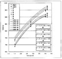
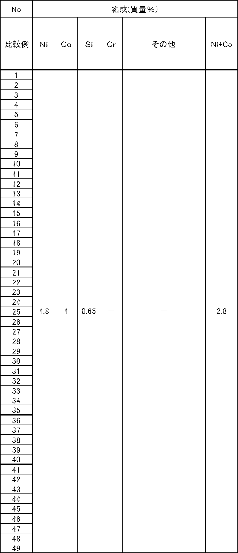
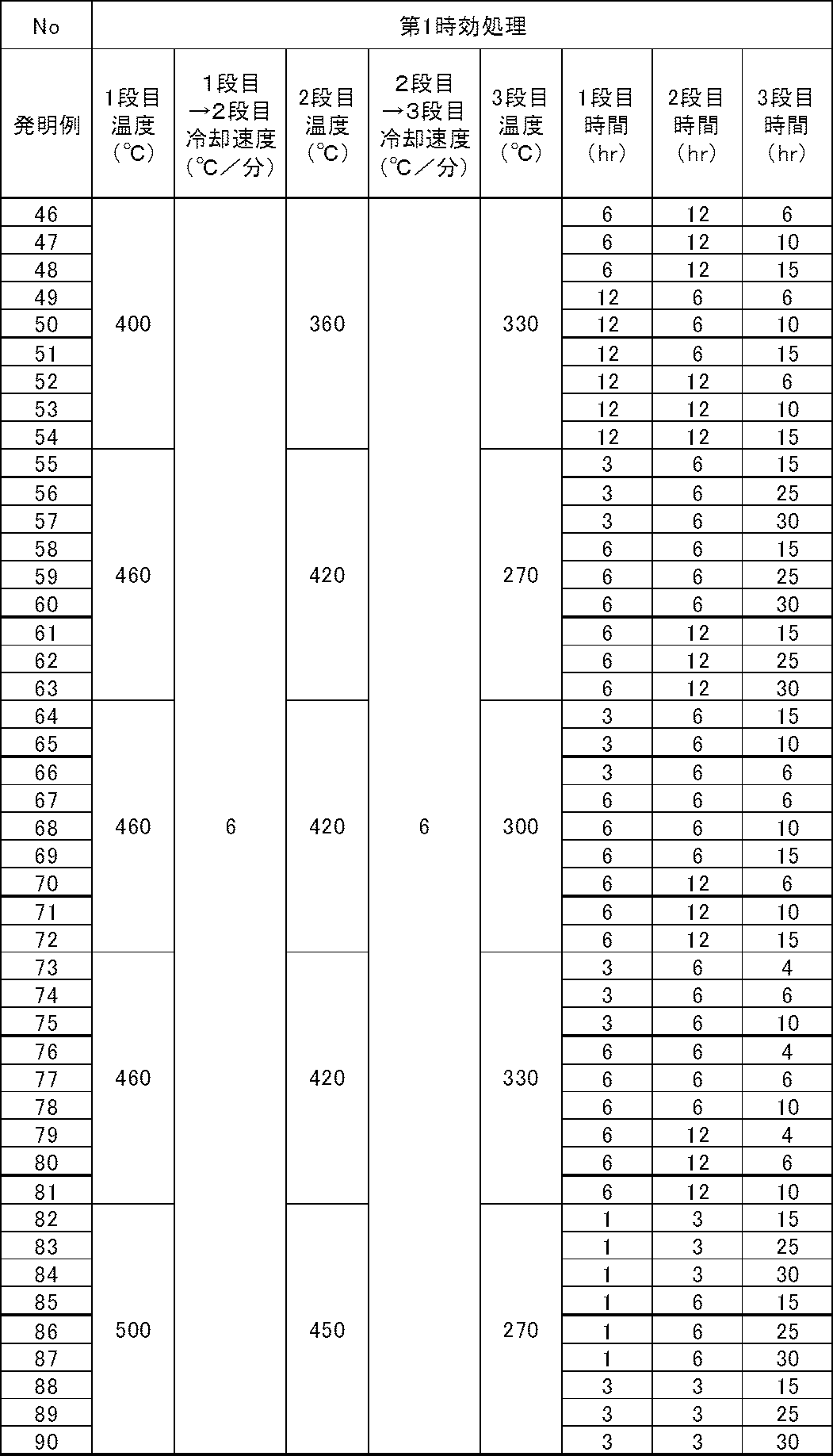
- Invention Example No. 137-139, no. 143 to 145, no. 149-151 and Comparative Example No. 174, 178, and 182 are graphs in which the total mass% concentration of Ni and Co (Ni + Co) is plotted on the x axis and YS is plotted on the y axis.
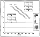
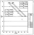
- Invention Example No. 140-142, no. 146-148, no. 152 to 154 and Comparative Example No. 175, 179, and 183 are graphs in which the total mass% concentration of Ni and Co (Ni + Co) is plotted on the x axis and YS is plotted on the y axis.
- Addition amounts of Ni, Co, and Si Ni, Co, and Si form an intermetallic compound by performing an appropriate heat treatment, and can increase the strength without deteriorating conductivity.
- the addition amounts of Ni, Co and Si are less than Ni: 1.0% by mass, Co: less than 0.5% by mass, and Si: less than 0.3% by mass, the desired strength cannot be obtained. If it exceeds 2.5% by mass, Co: more than 2.5% by mass, and Si: more than 1.2% by mass, the strength can be increased, but the electrical conductivity is remarkably lowered, and the hot workability is further deteriorated. Therefore, the addition amounts of Ni, Co, and Si were set to Ni: 1.0 to 2.5 mass%, Co: 0.5 to 2.5 mass%, and Si: 0.3 to 1.2 mass%.
- the addition amounts of Ni, Co, and Si are preferably Ni: 1.5 to 2.0 mass%, Co: 0.5 to 2.0 mass%, and Si: 0.5 to 1.0 mass%.
- the ratio [Ni + Co] / Si of the total mass concentration of Ni and Co with respect to the mass concentration of Si is too low, that is, if the ratio of Si to Ni and Co is too high, the conductivity will be increased by solute Si. In the annealing process, an oxide film of SiO 2 is formed on the material surface layer and the solderability is deteriorated. On the other hand, if the ratio of Ni and Co to Si is too high, the Si required for silicide formation is insufficient and it is difficult to obtain high strength.
- the [Ni + Co] / Si ratio in the alloy composition is preferably controlled within the range of 4 ⁇ [Ni + Co] / Si ⁇ 5, and should be controlled within the range of 4.2 ⁇ [Ni + Co] /Si ⁇ 4.7. Is more preferable.
- the added amount Cr of Cr preferentially precipitates at the grain boundaries in the cooling process during melt casting, so that the grain boundaries can be strengthened, cracks during hot working are less likely to occur, and yield reduction can be suppressed. That is, Cr that has precipitated at the grain boundaries during melt casting is re-dissolved by solution treatment or the like, but during subsequent aging precipitation, precipitated particles having a bcc structure mainly composed of Cr or a compound with Si are generated. In a normal Cu—Ni—Si alloy, Si that did not contribute to aging precipitation of the added Si amount suppresses the increase in conductivity while being dissolved in the matrix, but the silicide-forming element Cr is reduced.
- the amount of dissolved Si can be reduced, and the conductivity can be increased without impairing the strength.
- Cr concentration exceeds 0.5% by mass, coarse second-phase particles are easily formed, so that product characteristics are impaired. Therefore, Cr can be added to the Cu—Ni—Si—Co based copper alloy according to the present invention in a maximum amount of 0.5 mass%.
- the effect is small if it is less than 0.03% by mass, it is preferably added in an amount of 0.03 to 0.5% by mass, more preferably 0.09 to 0.3% by mass.
- the effect of addition is exhibited mainly by solid solution in the matrix phase, but further effects can be exhibited by inclusion in the second phase particles.
- the total concentration of Mg, Mn, Ag and P exceeds 2.0% by mass, the effect of improving characteristics is saturated and manufacturability is impaired. Therefore, in the Cu—Ni—Si—Co based copper alloy according to the present invention, a total of one or more selected from Mg, Mn, Ag and P is 2.0 mass% in total, preferably 1 maximum. .5% by mass can be added.
- the effect is small if it is less than 0.01% by mass, it is preferable to add 0.01 to 1.0% by mass in total, more preferably 0.04 to 0.5% by mass in total.
- the addition of a small amount improves product properties such as strength, stress relaxation properties, and plating properties without impairing electrical conductivity.
- the effect of addition is exhibited mainly by solid solution in the matrix.
- the total amount of Sn and Zn exceeds 2.0% by mass, the effect of improving characteristics is saturated and manufacturability is impaired. Therefore, the Cu—Ni—Si—Co based copper alloy according to the present invention can be added with a total of one or two selected from Sn and Zn up to a maximum of 2.0 mass%.
- the amount is less than 0.05% by mass, the effect is small. Therefore, it is preferable to add 0.05 to 2.0% by mass in total, and more preferably 0.5 to 1.0% by mass in total.
- Addition amounts of As, Sb, Be, B, Ti, Zr, Al, and Fe As, Sb, Be, B, Ti, Zr, Al, and Fe are also adjusted according to required product characteristics. This improves product properties such as conductivity, strength, stress relaxation properties, and plating properties.
- the effect of addition is exhibited mainly by solid solution in the parent phase, but it can also be exhibited by forming the second phase particles having a new composition or contained in the second phase particles. However, if the total amount of these elements exceeds 2.0% by mass, the effect of improving characteristics is saturated and manufacturability is impaired.
- the total of one or more selected from As, Sb, Be, B, Ti, Zr, Al and Fe is 2. 0% by mass can be added. However, since the effect is small if it is less than 0.001% by mass, it is preferable to add 0.001 to 2.0% by mass in total, more preferably 0.05 to 1.0% by mass in total.
- the total amount of Mg, Mn, Ag, P, Sn, Zn, As, Sb, Be, B, Ti, Zr, Al and Fe exceeds 3.0% by mass, manufacturability is easily impaired.
- the total of these is 2.0% by mass or less, more preferably 1.5% by mass or less.
- the copper alloy according to the present invention has a ⁇ 200 ⁇ pole as a result of obtaining the ratio of the diffraction intensity to ⁇ to the copper powder in each ⁇ of the X-ray diffraction pole figure measurement based on the rolling surface.
- the pure copper standard powder is defined as a copper powder having a purity of 99.5% with a 325 mesh (JIS Z8801).
- the copper alloy according to the present invention is a ⁇ 111 ⁇ pole as a result of obtaining a ratio of diffraction intensity to ⁇ to copper powder in each ⁇ of X-ray diffraction pole figure measurement based on the rolling surface.
- the pure copper standard powder is defined as a copper powder having a purity of 99.5% with a 325 mesh (JIS Z8801).
- the ⁇ -axis scan is performed in steps with respect to the 2 ⁇ value of the focused ⁇ hkl ⁇ Cu surface (the scanning angle 2 ⁇ of the detector is fixed).
- the sample is scanned on the ⁇ axis with respect to the angle ⁇ value (in-plane rotation (rotation) from 0 to 360 °).
- the direction perpendicular to the sample surface is defined as ⁇ 90 °, which is used as a measurement reference.
- the pole figure is measured by the reflection method ( ⁇ : ⁇ 15 ° to 90 °).
- the copper alloy strip according to the present invention has a Ni content (mass%) of [Ni], a Co content (mass%) of [Co], and a 0.2% proof stress of YS (MPa). Then, the formula a: ⁇ 11 ⁇ ([Ni] + [Co]) 2 + 146 ⁇ ([Ni] + [Co]) + 564 ⁇ YS ⁇ ⁇ 21 ⁇ ([Ni] + [Co]) 2 +202 X ([Ni] + [Co]) + 436 can be satisfied.
- the copper alloy strip according to the present invention has the formula a ′: ⁇ 11 ⁇ ([Ni] + [Co]) 2 + 146 ⁇ ([Ni] + [Co]) + 554 ⁇ YS ⁇ ⁇ 21 ⁇ ([[ Ni] + [Co]) 2 + 202 ⁇ ([Ni] + [Co]) + 441 can be satisfied.
- the copper alloy strip according to the present invention has the formula a ′′: ⁇ 11 ⁇ ([Ni] + [Co]) 2 + 146 ⁇ ([Ni] + [Co]) + 544 ⁇ YS ⁇ ⁇ 21 ⁇ ( [Ni] + [Co]) 2 + 202 ⁇ ([Ni] + [Co]) + 450 can be satisfied.
- the copper alloy strip containing 0.03 to 0.5 mass% of Cr according to the present invention has a Ni content (mass%) of [Ni] and a Co content (mass%) of [ Co], where 0.2% proof stress is YS (MPa), the formula A: ⁇ 14 ⁇ ([Ni] + [Co]) 2 + 164 ⁇ ([Ni] + [Co]) + 551 ⁇ YS ⁇ ⁇ 22 ⁇ ([Ni] + [Co]) 2 + 204 ⁇ ([Ni] + [Co]) + 447 can be satisfied.
- a copper alloy strip containing 0.03 to 0.5% by mass of Cr according to the present invention has the formula A ′: ⁇ 14 ⁇ ([Ni] + [Co]) 2 + 164 ⁇ ([Ni] + [Co]) + 541 ⁇ YS ⁇ ⁇ 22 ⁇ ([Ni] + [Co]) 2 + 204 ⁇ ([Ni] + [Co]) + 452 can be satisfied.
- the copper alloy strip containing 0.03 to 0.5% by mass of Cr according to the present invention is represented by the formula A ′′: ⁇ 14 ⁇ ([Ni] + [Co]) 2 + 164 ⁇ ([Ni ] + [Co]) + 531 ⁇ YS ⁇ ⁇ 21 ⁇ ([Ni] + [Co]) 2 + 198 ⁇ ([Ni] + [Co]) + 462.
- the copper alloy strip according to the present invention has a drooping curl in a direction parallel to the rolling direction of 35 mm or less, preferably 20 mm or less, more preferably 15 mm or less, for example, 10 to 30 mm.
- the drooping curl in the direction parallel to the rolling direction is obtained by the following procedure. A strip-shaped measurement sample having a length of 500 mm in the longitudinal direction parallel to the rolling direction and a length of 10 mm in the width direction perpendicular to the rolling direction is cut out from the strip to be tested, and one end of the sample in the longitudinal direction is gripped.
- the other end is suspended downward, the amount of warping of the other end with respect to the vertical line is measured, and this is defined as a suspended curl.
- the drooping curl is measured as described above.
- the length in the longitudinal direction parallel to the rolling direction is 500 to 1000 mm, and the length in the width direction perpendicular to the rolling direction is 10 to 50 mm. If the sample is an elongated sample having a, the measurement result of the drooping curl is almost the same.
- the copper alloy strip according to the present invention is 673 ⁇ YS ⁇ 976, 42.5 ⁇ EC ⁇ 57, where 0.2% proof stress is YS (MPa) and electrical conductivity is EC (% IACS). .5, Formula C: ⁇ 0.0563 ⁇ [YS] + 94.1972 ⁇ EC ⁇ ⁇ 0.0563 ⁇ [YS] +98.7040 is satisfied.
- the copper alloy strip according to the present invention is 683 ⁇ YS ⁇ 966, 43 ⁇ EC ⁇ 57, formula C ′: ⁇ 0.0563 ⁇ [YS] + 94.7610 ⁇ EC ⁇ ⁇ 0.0563 ⁇ [YS ] +98.1410 is satisfied.
- the copper alloy strip according to the present invention has 693 ⁇ YS ⁇ 956, 43.5 ⁇ EC ⁇ 56.5, formula C ”: ⁇ 0.0563 ⁇ [YS] + 955.3240 ⁇ EC ⁇ ⁇ 0. 0563 ⁇ [YS] +97.5770 is satisfied.
- a copper alloy strip containing 0.03 to 0.5 mass% of Cr according to the present invention has a 0.2% yield strength of YS (MPa) and a conductivity of EC (% IACS). 679 ⁇ YS ⁇ 982, 43.5 ⁇ EC ⁇ 59.5, and formula D: ⁇ 0.0610 ⁇ [YS] + 99.7465 ⁇ EC ⁇ ⁇ 0.0610 ⁇ [YS] +104.6291 is satisfied.
- a copper alloy strip containing 0.03 to 0.5% by mass of Cr according to the present invention is 689 ⁇ YS ⁇ 972, 44 ⁇ EC ⁇ 59, formula d ′: ⁇ 0.0610 ⁇ [YS + 100.3568 ⁇ EC ⁇ ⁇ 0.0610 ⁇ [YS] +104.0188.
- 699 ⁇ YS ⁇ 962, 44.5 ⁇ EC ⁇ 58.5, formula d ”: ⁇ 0.0610 ⁇ [YS] + 100.9671 ⁇ EC ⁇ ⁇ 0 0.0610 ⁇ [YS] +103.4085 is satisfied.
- the second-phase particle mainly refers to silicide, but is not limited to this.
- Crystallized substances generated in the solidification process of melt casting and precipitation generated in the subsequent cooling process This refers to precipitates generated in the cooling process after hot rolling, precipitates generated in the cooling process after solution treatment, and precipitates generated in the aging process.
- the distribution of second phase particles having a particle size of 0.1 ⁇ m or more and 1 ⁇ m or less is controlled. This further improves the balance of strength, conductivity and drooping curl.
- the number density of the second phase particles having a particle diameter of 0.1 ⁇ m or more and 1 ⁇ m or less is 5 ⁇ 10 5 to 1 ⁇ 10 7 particles / mm 2 , preferably 1 ⁇ 10 6 to 10 ⁇ 10 6 particles. / Mm 2 , more preferably 5 ⁇ 10 6 to 10 ⁇ 10 6 / mm 2 .
- the particle size of the second phase particles refers to the diameter of the smallest circle surrounding the particles when the second phase particles are observed under the following conditions.
- the number density of second phase particles with a particle size of 0.1 ⁇ m or more and 1 ⁇ m or less can be observed by using an electron microscope that can observe particles at high magnification (eg, 3000 times) such as FE-EPMA and FE-SEM and image analysis software. The number and particle size can be measured.
- the sample material may be adjusted by etching the matrix phase under the general electropolishing conditions such that the particles precipitated with the composition of the present invention are not dissolved to reveal the second phase particles.
- the observation surface has no specified rolling surface or cross section of the specimen.
- a Corson copper alloy In a general manufacturing process of a Corson copper alloy, first, an atmospheric melting furnace is used to melt raw materials such as electrolytic copper, Ni, Si, and Co to obtain a molten metal having a desired composition. Then, casting the molten metal into an ingot. Thereafter, hot rolling is performed, and cold rolling and heat treatment are repeated to finish a strip or foil having a desired thickness and characteristics.
- Heat treatment includes solution treatment and aging treatment. In the solution treatment, heating is performed at a high temperature of about 700 to about 1000 ° C. to cause the second phase particles to be dissolved in the Cu matrix and simultaneously to recrystallize the Cu matrix. The solution treatment may be combined with hot rolling.
- the second phase particles that are heated in the temperature range of about 350 to about 550 ° C. for 1 hour or more and solid-dissolved by the solution treatment are precipitated as fine particles of nanometer order.
- This aging treatment increases strength and conductivity.
- cold rolling may be performed before and / or after aging.
- strain relief annealing low temperature annealing
- grinding, polishing, shot blast pickling and the like for removing oxide scale on the surface are appropriately performed.
- the copper alloy according to the present invention also undergoes the manufacturing process described above. However, in order for the finally obtained copper alloy to have the characteristics specified in the present invention, the solution treatment and subsequent steps are strictly performed. It is important to control. Unlike the conventional Cu-Ni-Si-based Corson alloy, the Cu-Ni-Co-Si-based alloy of the present invention is Co (which in some cases is difficult to control second phase particles as an essential component for age precipitation hardening) Further, this is because Cr) is positively added. Co forms secondary phase particles together with Ni and Si because the generation and growth rate is sensitive to the holding temperature and cooling rate during heat treatment.
- Hot rolling is performed after holding at 950 ° C. to 1050 ° C. for 1 hour or longer, and if the temperature at the end of hot rolling is 850 ° C. or higher, even if Co and further Cr are added, it is dissolved in the matrix. be able to.
- the temperature condition of 950 ° C. or higher is a higher temperature setting than other Corson alloys. If the holding temperature before hot rolling is less than 950 ° C., solid solution is insufficient, and if it exceeds 1050 ° C., the material may be dissolved.
- the cooling rate when the material temperature decreases from 850 ° C. to 400 ° C. is 15 ° C./s or more, preferably 18 ° C./s or more, for example, 15 to 25 ° C./s.
- the temperature is preferably 15 to 20 ° C./s.
- the “average cooling rate from 850 ° C. to 400 ° C.” after hot rolling is the time when the material temperature decreases from 850 ° C. to 400 ° C., and “(850 ⁇ 400) (° C. ) / Cooling time (s) ”.
- the purpose of the solution treatment is to increase the age-hardening ability after the solution treatment by solidifying the crystallized particles at the time of dissolution casting and the precipitated particles after hot rolling.
- the holding temperature and time during the solution treatment and the cooling rate after holding are important.
- the solution treatment may be carried out in either a continuous furnace or a batch furnace, but it is preferably carried out in a continuous furnace from the viewpoint of production efficiency when industrially producing the strip material as in the present invention.
- the cooling after the solution treatment is preferably rapid cooling. Specifically, after solution treatment at 850 ° C. to 1050 ° C. for 10 to 3600 seconds, the average cooling rate is 10 ° C./second or more, preferably 15 ° C. or more, more preferably 20 ° C./second or more, and cooling to 400 ° C. Is effective. However, if the average cooling rate is too high, the effect of increasing the strength cannot be obtained sufficiently.
- the “average cooling rate” is a value (° C./second) obtained by measuring the cooling time from the solution temperature to 400 ° C. and calculating “(solution temperature ⁇ 400) (° C.) / Cooling time (second)”. ).
- the cooling condition after the solution treatment it is more preferable to use a two-stage cooling condition as described in Patent Document 1. That is, after the solution treatment, it is preferable to adopt two-stage cooling in which 850 to 650 ° C. is slowly cooled and then 650 to 400 ° C. is rapidly cooled. This further improves strength and conductivity.
- the average cooling rate when the material temperature decreases from the solution treatment temperature to 650 ° C. is 1 ° C./s or more and less than 15 ° C./s, preferably 5 ° C.
- the average cooling rate when the temperature is decreased from 650 ° C. to 400 ° C. is controlled to 15 ° C./s or more, preferably 18 ° C./s or more, for example, 15 to 25 ° C./s. Specifically, it is set to 15 to 20 ° C./s. Since the precipitation of the second phase particles is remarkable up to about 400 ° C., the cooling rate at less than 400 ° C. is not a problem.
- the cooling rate after solution treatment is controlled by adjusting the holding time by providing a slow cooling zone and a cooling zone adjacent to the heating zone heated to the range of 850 ° C to 1050 ° C. can do.
- rapid cooling water cooling may be applied to the cooling method, and in the case of slow cooling, a temperature gradient may be created in the furnace.
- the “average cooling rate until the temperature decreases to 650 ° C.” after the solution treatment is the cooling time when the temperature decreases from the material temperature maintained in the solution treatment to 650 ° C., “(solution treatment temperature ⁇ 650) (° C.) / Cooling time (s) "means a value (° C / s) calculated.
- the “average cooling rate when the temperature decreases from 650 ° C. to 400 ° C.” means a value (° C./s) calculated by “(650 ⁇ 400) (° C.) / Cooling time (s)”.
- Water cooling is the most effective way to speed up cooling. However, since the cooling rate varies depending on the temperature of the water used for water cooling, the cooling can be further accelerated by managing the water temperature. Since the desired cooling rate may not be obtained when the water temperature is 25 ° C. or higher, it is preferably maintained at 25 ° C. or lower. When a material is placed in a tank in which water is stored and cooled with water, the temperature of the water rises and tends to be 25 ° C. or higher, so that the material is cooled in a mist (shower) at a constant water temperature (25 ° C. or lower).
- the cooling rate can also be increased by adding water cooling nozzles or increasing the amount of water per unit time.
- an aging treatment, a cold rolling and an optional temper annealing are sequentially performed after the solution treatment, and the aging treatment is performed at a specific temperature and It is effective to carry out with three-stage aging according to time conditions. That is, by adopting three-stage aging, strength and conductivity are improved, and then cold rolling is performed to reduce drooping curl.
- the strength and conductivity were significantly improved by changing the aging treatment after solution treatment to three-stage aging.
- the growth of the second phase particles precipitated in the first and second stages and the precipitation in the third stage This is considered to be because the work strain is easily accumulated by the rolling of the next step due to the second phase particles.
- the material temperature is heated to 400 to 500 ° C. for 1 to 12 hours, preferably the material temperature is set to 420 to 480 ° C. and heated for 2 to 10 hours, more preferably the material temperature is set to 440 to 460 ° C. Perform the first stage of heating for 3-8 hours.
- the purpose of the first stage is to increase the strength and conductivity by nucleation and growth of the second phase particles.
- the volume fraction of the second phase particles is small, and it is difficult to obtain desired strength and conductivity.
- the volume fraction of the second phase particles increases, but it tends to coarsen and the strength decreases. Becomes stronger.
- the cooling rate is 1 to 8 ° C./min, preferably 3 to 8 ° C./min, more preferably 6 to 8 ° C./min, and the aging temperature of the second stage is shifted.
- the reason for setting such a cooling rate is to prevent the second phase particles precipitated in the first stage from growing excessively.
- the cooling rate here is measured by (first stage aging temperature-second stage aging temperature) (° C) / (cooling time from first stage aging temperature to second stage aging temperature (minutes)).
- the material temperature is heated at 350 to 450 ° C. for 1 to 12 hours, preferably the material temperature is heated at 380 to 430 ° C. for 2 to 10 hours, more preferably the material temperature is heated at 400 to 420 ° C. for 3 to 8 hours.
- the second stage In the second stage, the second phase particles precipitated in the first stage are grown within a range that contributes to strength, and the second phase particles are newly precipitated in the second stage (in the first stage). The purpose is to increase the strength and conductivity by being smaller than the precipitated second phase particles.
- the second phase particles precipitated in the first stage cannot grow, so it is difficult to increase the conductivity. Since the second phase particles cannot be newly deposited, the strength and conductivity cannot be increased. On the other hand, when heated until the material temperature exceeds 450 ° C., or when the heating time exceeds 12 hours, the second phase particles precipitated in the first stage grow too much and become coarse, and the strength decreases. End up.
- the temperature difference between the first stage and the second stage should be 20 to 60 ° C., preferably 20 to 50 ° C., more preferably 20 to 40 ° C.
- the cooling rate is 1 to 8 ° C./min, preferably 3 to 8 ° C./min, more preferably 6 to 8 ° C./min. Move to temperature.
- the cooling rate here is measured by (second stage aging temperature-third stage aging temperature) (° C) / (cooling time from second stage aging temperature to third stage aging temperature (min)).
- the material temperature is heated to 260 to 340 ° C. for 4 to 30 hours, preferably the material temperature is heated to 290 to 330 ° C. for 6 to 25 hours, more preferably the material temperature is set to 300 to 320 ° C. and heated for 8 to 20 hours.
- the purpose of the third stage is to slightly grow the second phase particles precipitated in the first and second stages and to newly generate second phase particles.
- the material temperature in the third stage is less than 260 ° C. or the heating time is less than 4 hours, the second phase particles precipitated in the first stage and the second stage cannot be grown. Therefore, it is difficult to obtain desired strength, conductivity, and spring limit value.
- the second phase particles precipitated in the first and second stages grow too much and become coarse. Therefore, it is difficult to obtain a desired strength.
- the temperature difference between the second stage and the third stage should be 20 to 180 ° C., preferably 50 to 135 ° C., and more preferably 70 to 120 ° C.
- each step is performed within a temperature fluctuation range of 10 ° C. or less.
- the degree of processing (rolling ratio) at this time is preferably 10 to 80%, more preferably 20 to 60% in order to reach a desired strength level and reduce curling. If the degree of work is too high, there is a problem that bending workability is deteriorated. Conversely, if the degree of work is too low, suppression of drooping curl tends to be insufficient.
- temper annealing a temperature range of 200 ° C. to 500 ° C. is set to 1 second to 1000 seconds. By performing the temper annealing, the effect of improving the spring property can be obtained.
- the Cu—Ni—Si—Co based copper alloy strip of the present invention can be processed into various copper products, for example, plates, foils, tubes, bars and wires, and the Cu—Ni—Si—Co according to the present invention.
- the copper alloy can be used after being processed into electronic parts such as lead frames, connectors, pins, terminals, relays, switches, and secondary battery foils.
- the thickness of the copper alloy strip according to the present invention is not particularly limited, but is, for example, 0.005 mm to 1.500 mm. Further, it is preferably 0.030 mm to 0.900 mm, more preferably 0.040 mm to 0.800 mm, and particularly preferably 0.050 mm to 0.400 mm.
- Copper alloy (10 kg) containing each additive element listed in Table 1 and the balance consisting of copper and impurities is melted at 1300 ° C. in a high-frequency melting furnace, and an ingot with a thickness of 30 mm Cast into. Next, this ingot was heated in a batch furnace at 1000 ° C. for 3 hours, then hot-rolled to a plate thickness of 10 mm at an ascending temperature (hot rolling end temperature) of 900 ° C., and immediately after completion of hot rolling, 15 ° C./s. At a cooling rate of 400 ° C. Thereafter, it was allowed to cool in the air.
- a plate having a length of 80 m, a width of 50 mm and a thickness of 0.286 mm was formed by cold rolling.
- solution treatment was performed at 950 ° C. for 120 seconds in a continuous furnace, and then cooled.
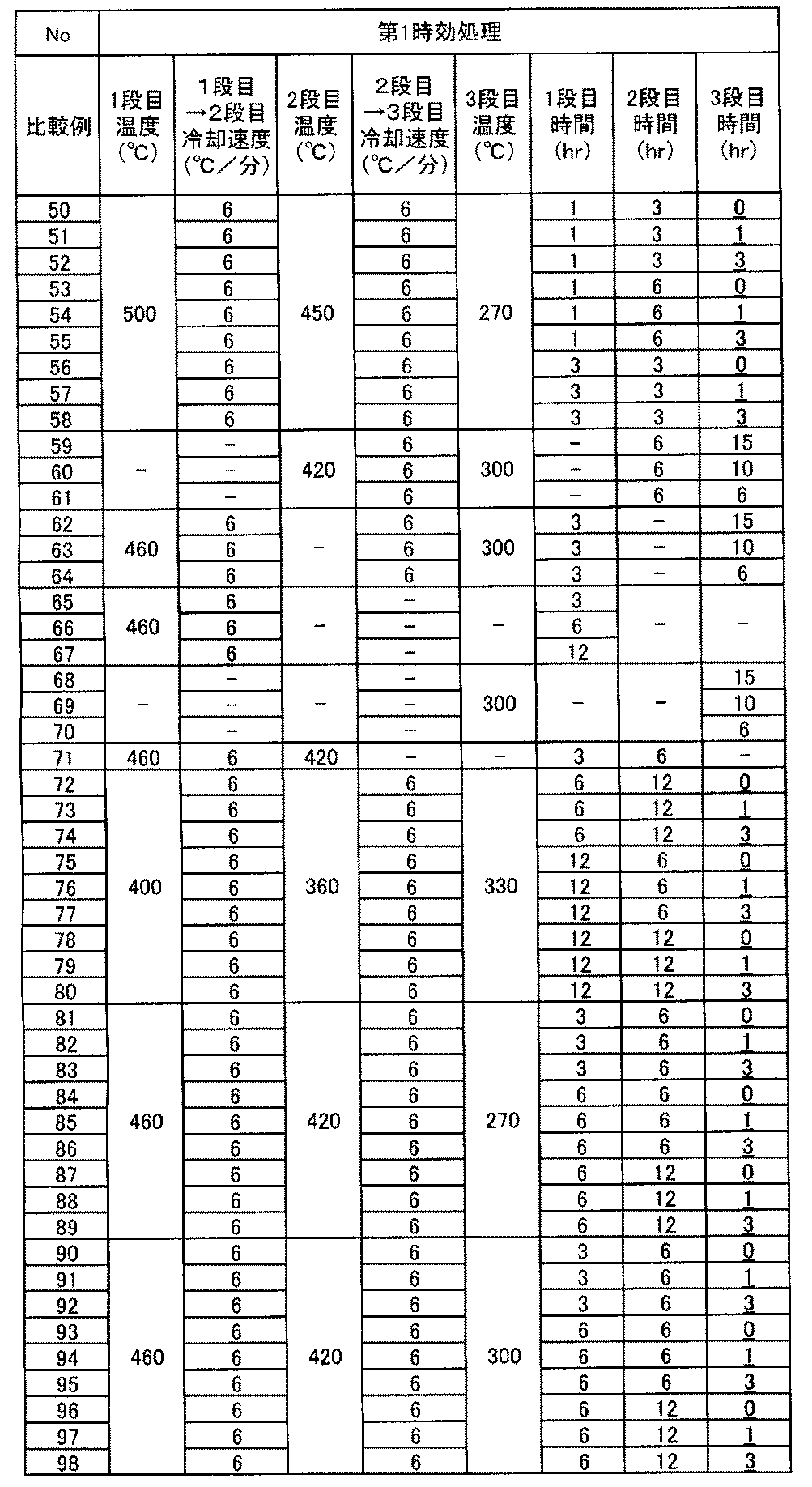
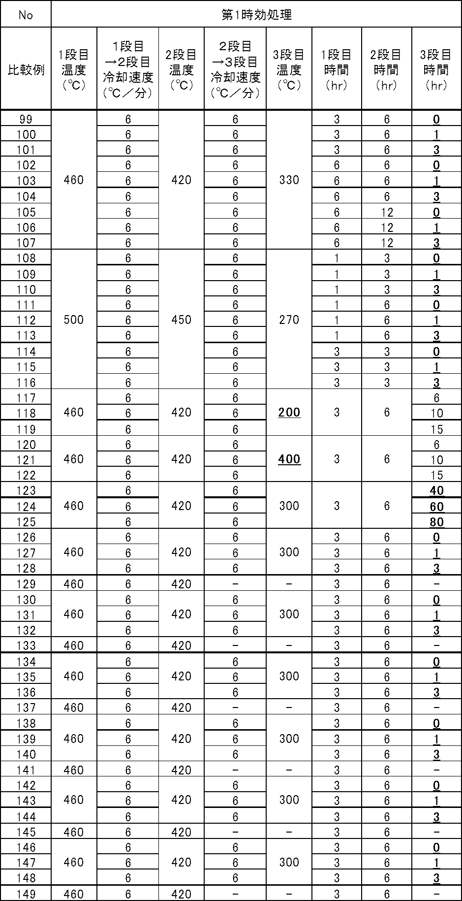
- the cooling conditions were as in Example No. 1 to 136 and Comparative Example No. 1 to 173 and 186 to 191 were water-cooled with an average cooling rate from the solution temperature to 400 ° C. being 20 ° C./s. 137-154 and Comparative Example No. In 174 to 185, the cooling rate from the solution treatment temperature to 650 ° C.
- the surface of the material is electropolished to dissolve the Cu matrix, and the second phase particles remain undissolved. did.
- the electrolytic polishing liquid used was a mixture of phosphoric acid, sulfuric acid, and pure water in an appropriate ratio.
- FE-EPMA electrolytic radiation type EPMA: JXA-8500F manufactured by JEOL Ltd.
- acceleration voltage is 5 to 10 kV
- sample current is 2 ⁇ 10 ⁇ 8 to 10 ⁇ 10 A
- spectral crystals are LDE, TAP, PET .
- the electrical conductivity (EC;% IACS) was determined by volume resistivity measurement using a double bridge according to JIS H0505.
- the drooping curl was obtained by the measurement method described above.
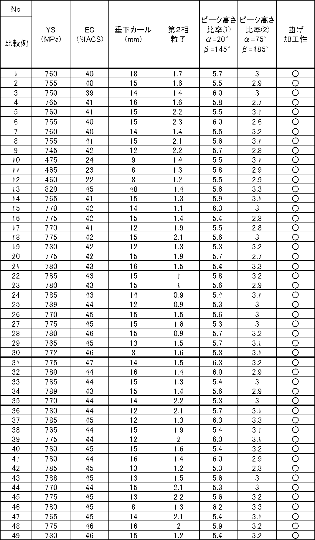
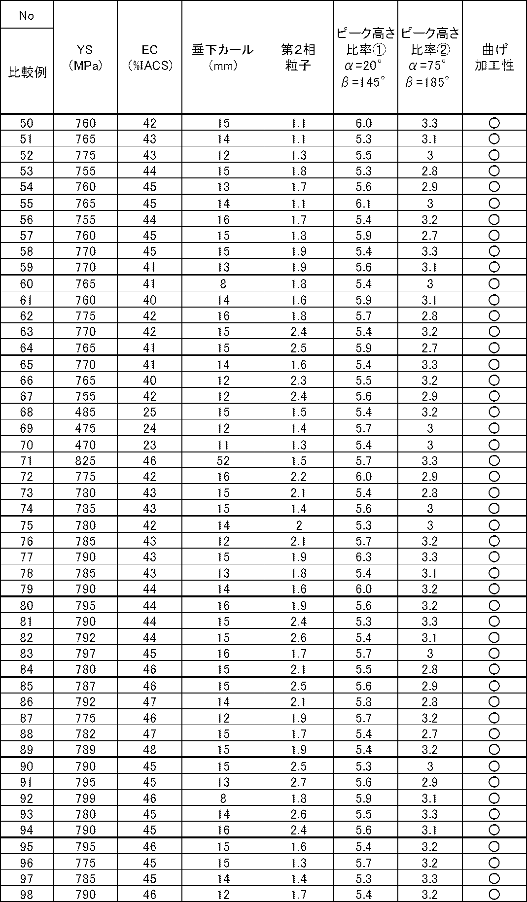
- Table 4 shows the test results of each test piece.
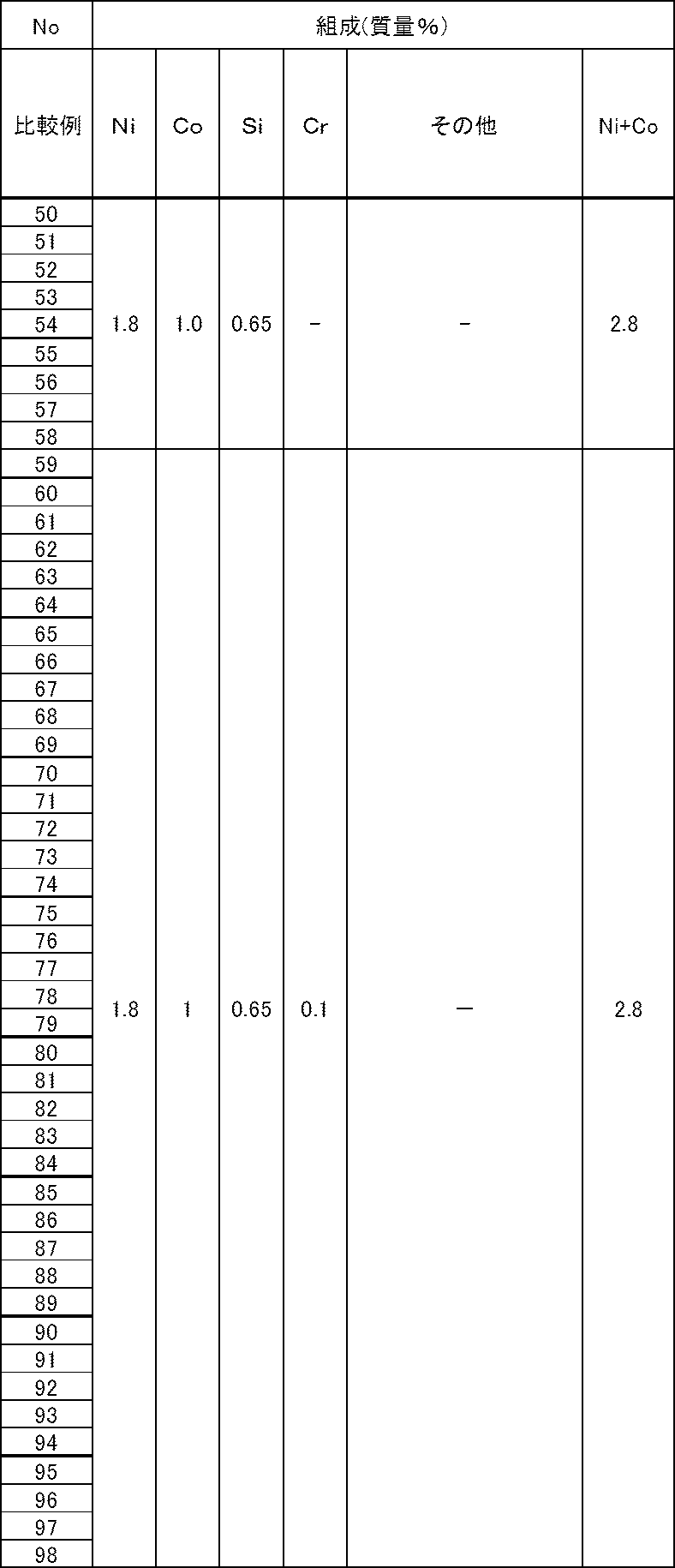
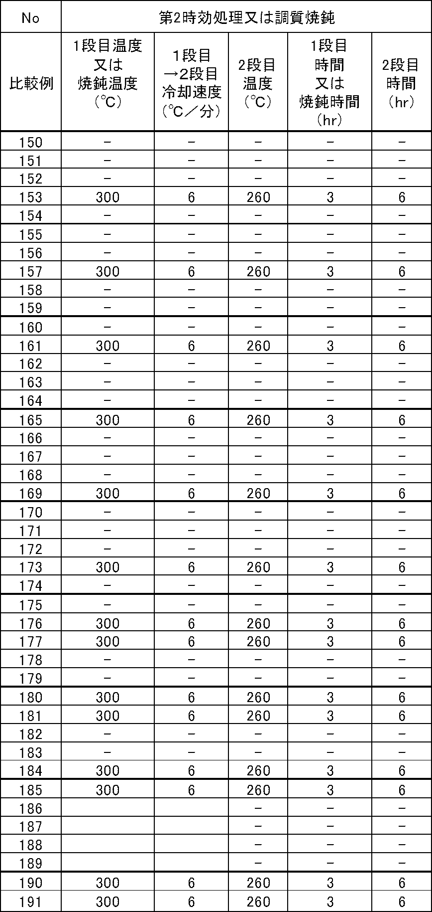
- Comparative Example No. 7 to 12 65 to 70, 174, 175, 178, 179, 182, and 183 are examples in which the first aging is performed by one-stage aging. Comparative Example No.
- Comparative Example No. 120 to 122 are examples in which the aging temperature in the third stage was high. Comparative Example No. 123 to 125 are examples in which the aging time of the third stage is long. Comparative Example No. Reference numerals 186 and 187 are examples in which the cooling rate from the first stage to the second stage, the second stage to the third stage is too high. Comparative Example No. 188 and 189 are examples in which the cooling rate from the first stage to the second stage, the second stage to the third stage is too low. Comparative Example No. 190 and 191 are the same as the steps of the invention example until the cold rolling is performed after the first aging treatment, but the second aging treatment and the cold rolling are performed thereafter. Comparative Example No.
- Inventive Example was changed cooling conditions after solution treatment to the preferred conditions No. 137-154 and Comparative Example No.
- plots of the total mass% concentration of Ni and Co (Ni + Co) on the x-axis and YS on the y-axis are shown in FIG. 1 (without Cr addition) and FIG. 2 (with Cr addition).
- FIGS. 3 (without Cr addition) and FIG. 4 (with Cr addition) show plots of the total mass% Co concentration (Ni + Co) on the x-axis and EC on the y-axis, respectively.
- FIG. 1 without Cr addition
- FIG. 2 with Cr addition
- FIGS. 3 (without Cr addition) and FIG. 4 (with Cr addition) show plots of the total mass% Co concentration (Ni + Co) on the x-axis and EC on the y-axis, respectively.
Landscapes
- Chemical & Material Sciences (AREA)
- Engineering & Computer Science (AREA)
- Mechanical Engineering (AREA)
- Materials Engineering (AREA)
- Metallurgy (AREA)
- Organic Chemistry (AREA)
- Physics & Mathematics (AREA)
- Thermal Sciences (AREA)
- Crystallography & Structural Chemistry (AREA)
- Conductive Materials (AREA)
- Non-Insulated Conductors (AREA)
Abstract
Description
当該文献に記載の銅合金を製造する方法として、
-所望の組成をもつインゴットを溶解鋳造する工程1と、
-950℃以上1050℃以下で1時間以上加熱後に熱間圧延を行い、熱間圧延終了時の温度を850℃以上とし、850℃から400℃までの平均冷却速度を15℃/s以上として冷却する工程2と、
-冷間圧延工程3と、
-850℃以上1050℃以下で溶体化処理を行い、材料温度が650℃に低下するまでの平均冷却速度を1℃/s以上15℃/s未満として冷却し、650℃から400℃まで低下するときの平均冷却速度を15℃/s以上として冷却する工程4と、
-425℃以上475℃未満で1~24時間行う第一の時効処理工程5と、
-冷間圧延工程6と、
-100℃以上350℃未満で1~48時間行う第二の時効処理工程5と、
を順に行なうことを含む製造方法が開示されている。
一方、特許文献3に記載の銅合金製造方法をCu-Ni-Si-Co系銅合金条の工業的生産に応用した場合、垂下カールの問題は生じないが、強度及び導電率のバランスが不十分であることを見出した。
そして、当該方法によって得られた銅合金条は、圧延面を基準としたX線回折極点図測定の各αにおいて、βに対する回折強度の銅粉末に対する比を求めた結果、{200}極点図においてα=20°、β=145°に見られるピーク高さの標準銅粉末のそれに対する比率が5.2倍以下であり、なおかつ、{111}極点図においてα=75°、β=185°に見られるピーク高さの標準銅粉末のそれに対する比率が3.4倍以上であるという特異性を有することを見出した。このような回折ピークが得られた理由は不明であるが、第二相粒子の微細な分布状態が影響を与えていると考えられる。
(a){200}極点図においてα=20°におけるβ走査による回折ピーク強度のうち、β角度145°のピーク高さが標準銅粉末のそれに対して5.2倍以下であること;
(b){111}極点図においてα=75°におけるβ走査による回折ピーク強度のうち、β角度185°のピーク高さが標準銅粉末のそれに対して3.4倍以上であること。
式ア:-11×([Ni]+[Co])2+146×([Ni]+[Co])+564≧YS≧-21×([Ni]+[Co])2+202×([Ni]+[Co])+436
を満たす。
673≦YS≦976、42.5≦EC≦57.5、式ウ:-0.0563×〔YS〕+94.1972≦EC≦-0.0563×〔YS〕+98.7040
を満たす。
式イ:-14×([Ni]+[Co])2+164×([Ni]+[Co])+551≧YS≧-22×([Ni]+[Co])2+204×([Ni]+[Co])+447
を満たす。
679≦YS≦982、43.5≦EC≦59.5、式エ:-0.0610×〔YS〕+99.7465≦EC≦-0.0610×〔YS〕+104.6291
を満たす。
更にMg、P、As、Sb、Be、B、Mn、Sn、Ti、Zr、Al、Fe、Zn及びAgの群から選ばれる少なくとも1種を総計で最大2.0質量%含有する。
-以下の(1)~(3)から選ばれる組成をもつインゴットを溶解鋳造する工程1と、
(1)Ni:1.0~2.5質量%、Co:0.5~2.5質量%、Si:0.3~1.2質量%を含有し、残部がCu及び不可避不純物からなる組成
(2)Ni:1.0~2.5質量%、Co:0.5~2.5質量%、Si:0.3~1.2質量%、Cr:0.03~0.5質量%を含有し、残部がCu及び不可避不純物からなる組成
(3)(1)又は(2)に、更にMg、P、As、Sb、Be、B、Mn、Sn、Ti、Zr、Al、Fe、Zn及びAgの群から選ばれる少なくとも1種を総計で最大2.0質量%含有する組成
-950℃以上1050℃以下で1時間以上加熱後に熱間圧延を行い、熱間圧延終了時の温度を850℃以上とし、850℃から400℃までの平均冷却速度を15℃/s以上として冷却する工程2と、
-冷間圧延工程3と、
-850℃以上1050℃以下で溶体化処理を行い、400℃までの平均冷却速度を毎秒10℃以上として冷却する工程4と、
-材料温度を400~500℃として1~12時間加熱する1段目と、次いで、材料温度を350~450℃として1~12時間加熱する2段目と、次いで、材料温度を260~340℃として4~30時間加熱する3段目を有し、1段目から2段目までの冷却速度及び2段目から3段目までの冷却速度はそれぞれ1~8℃/分とし、1段目と2段目の温度差を20~60℃とし、2段目と3段目の温度差を20~180℃としてバッチ炉で材料をコイル状に巻いたまま多段時効する時効処理工程5と、
-冷間圧延工程6と、
を順に行うことを含む上記銅合金条の製造方法である。
Ni、Co及びSiは、適当な熱処理を施すことにより金属間化合物を形成し、導電率を劣化させずに高強度化が図れる。
Ni、Co及びSiの添加量がそれぞれNi:1.0質量%未満、Co:0.5質量%未満、Si:0.3質量%未満では所望の強度が得られず、逆に、Ni:2.5質量%超、Co:2.5質量%超、Si:1.2質量%超では高強度化は図れるが導電率が著しく低下し、更には熱間加工性が劣化する。よってNi、Co及びSiの添加量はNi:1.0~2.5質量%、Co:0.5~2.5質量%、Si:0.3~1.2質量%とした。Ni、Co及びSiの添加量は好ましくは、Ni:1.5~2.0質量%、Co:0.5~2.0質量%、Si:0.5~1.0質量%である。
そのため、合金組成中の[Ni+Co]/Si比は4≦[Ni+Co]/Si≦5の範囲に制御することが好ましく、4.2≦[Ni+Co]/Si≦4.7の範囲に制御することがより好ましい。
Crは溶解鋳造時の冷却過程において結晶粒界に優先析出するため粒界を強化でき、熱間加工時の割れが発生しにくくなり、歩留低下を抑制できる。すなわち、溶解鋳造時に粒界析出したCrは溶体化処理などで再固溶するが、続く時効析出時にCrを主成分としたbcc構造の析出粒子またはSiとの化合物を生成する。通常のCu-Ni-Si系合金では添加したSi量のうち、時効析出に寄与しなかったSiは母相に固溶したまま導電率の上昇を抑制するが、珪化物形成元素であるCrを添加して、珪化物をさらに析出させることにより、固溶Si量を低減でき、強度を損なわずに導電率を上昇できる。しかしながら、Cr濃度が0.5質量%を超えると粗大な第二相粒子を形成しやすくなるため、製品特性を損なう。従って、本発明に係るCu-Ni-Si-Co系銅合金には、Crを最大で0.5質量%添加することができる。但し、0.03質量%未満ではその効果が小さいので、好ましくは0.03~0.5質量%、より好ましくは0.09~0.3質量%添加するのがよい。
Mg、Mn、Ag及びPは、微量の添加で、導電率を損なわずに強度、応力緩和特性等の製品特性を改善する。添加の効果は主に母相への固溶により発揮されるが、第二相粒子に含有されることで一層の効果を発揮させることもできる。しかしながら、Mg、Mn、Ag及びPの濃度の総計が2.0質量%を超えると特性改善効果が飽和するうえ、製造性を損なう。従って、本発明に係るCu-Ni-Si-Co系銅合金には、Mg、Mn、Ag及びPから選択される1種又は2種以上を総計で最大2.0質量%、好ましくは最大1.5質量%添加することができる。但し、0.01質量%未満ではその効果が小さいので、好ましくは総計で0.01~1.0質量%、より好ましくは総計で0.04~0.5質量%添加するのがよい。
Sn及びZnにおいても、微量の添加で、導電率を損なわずに強度、応力緩和特性、めっき性等の製品特性を改善する。添加の効果は主に母相への固溶により発揮される。しかしながら、Sn及びZnの総計が2.0質量%を超えると特性改善効果が飽和するうえ、製造性を損なう。従って、本発明に係るCu-Ni-Si-Co系銅合金には、Sn及びZnから選択される1種又は2種を総計で最大2.0質量%添加することができる。但し、0.05質量%未満ではその効果が小さいので、好ましくは総計で0.05~2.0質量%、より好ましくは総計で0.5~1.0質量%添加するのがよい。
As、Sb、Be、B、Ti、Zr、Al及びFeにおいても、要求される製品特性に応じて、添加量を調整することで、導電率、強度、応力緩和特性、めっき性等の製品特性を改善する。添加の効果は主に母相への固溶により発揮されるが、第二相粒子に含有され、若しくは新たな組成の第二相粒子を形成することで一層の効果を発揮させることもできる。しかしながら、これらの元素の総計が2.0質量%を超えると特性改善効果が飽和するうえ、製造性を損なう。従って、本発明に係るCu-Ni-Si-Co系銅合金には、As、Sb、Be、B、Ti、Zr、Al及びFeから選択される1種又は2種以上を総計で最大2.0質量%添加することができる。但し、0.001質量%未満ではその効果が小さいので、好ましくは総計で0.001~2.0質量%、より好ましくは総計で0.05~1.0質量%添加するのがよい。
本発明に係る銅合金は一実施形態において、圧延面を基準としたX線回折極点図測定の各αにおいて、βに対する回折強度の銅粉末に対する比を求めた結果で、{200}極点図においてα=20°、β=145°に見られるピーク高さの標準銅粉末のそれに対する比率が(以下、「α=20°におけるβ角度145°のピーク高さ比率」という。)が5.2倍以下である。
α=20°におけるβ角度145°のピーク高さ比率は好ましくは5.0倍以下であり、より好ましくは4.8倍以下であり、典型的には3.5~5.2である。純銅標準粉末は325メッシュ(JIS Z8801)の純度99.5%の銅粉末で定義される。
α=75°におけるβ角度185°のピーク高さ比率は好ましくは3.6倍以上であり、より好ましくは3.8倍以上であり、典型的には3.4~5.0である。純銅標準粉末は325メッシュ(JIS Z8801)の純度99.5%の銅粉末で定義される。
{111}Cu面の回折ピークでのα=75°におけるβ角度185°のピーク高さは、α=75°においてβ角度に対する強度をプロットして、β=185°のピーク値を読み取ることで測定でき、{200}Cu面の回折ピークでのα=20°におけるβ角度145°のピーク高さは、α=20°においてβ角度に対する強度をプロットして、β=145°のピーク値を読み取ることで測定できる。
本発明に係る銅合金条は一実施形態において、Niの含有量(質量%)を[Ni]、Coの含有量(質量%)を[Co]、0.2%耐力をYS(MPa)としたときに、式ア:-11×([Ni]+[Co])2+146×([Ni]+[Co])+564≧YS≧-21×([Ni]+[Co])2+202×([Ni]+[Co])+436を満たすことができる。
本発明に係る銅合金条は好ましい実施形態において、式ア’:-11×([Ni]+[Co])2+146×([Ni]+[Co])+554≧YS≧-21×([Ni]+[Co])2+202×([Ni]+[Co])+441を満たすことができる。
本発明に係る銅合金条は更に好ましい実施形態において、式ア”:-11×([Ni]+[Co])2+146×([Ni]+[Co])+544≧YS≧-21×([Ni]+[Co])2+202×([Ni]+[Co])+450を満たすことができる。
本発明に係るCrを0.03~0.5質量%を含有する銅合金条は好ましい実施形態において、式イ’:-14×([Ni]+[Co])2+164×([Ni]+[Co])+541≧YS≧-22×([Ni]+[Co])2+204×([Ni]+[Co])+452を満たすことができる。
本発明に係るCrを0.03~0.5質量%を含有する銅合金条は更に好ましい実施形態において、式イ”: -14×([Ni]+[Co])2+164×([Ni]+[Co])+531≧YS≧-21×([Ni]+[Co])2+198×([Ni]+[Co])+462を満たすことができる。
本発明において、圧延方向に平行な方向における垂下カールは以下の手順で求める。試験対象となる条材から、圧延方向に平行な長手方向に500mm×圧延方向に直角な幅方向に10mmの長さをもつ細長形状の測定用サンプルを切り出し、このサンプルの長手方向の一端を把持し、他端を下方へと垂下し、この他端の鉛直線に対する反り量を測定し、これを垂下カールとする。なお、本発明においては垂下カールを上記のように測定することとしているが、圧延方向に平行な長手方向の長さが500~1000mmで、圧延方向に直角な幅方向に10~50mmの長さをもつ細長形状のサンプルであれば、垂下カールの測定結果はほとんど変わらない。
本発明において、第二相粒子とは主にシリサイドを指すが、これに限られるものではなく、溶解鋳造の凝固過程に生ずる晶出物及びその後の冷却過程で生ずる析出物、熱間圧延後の冷却過程で生ずる析出物、溶体化処理後の冷却過程で生ずる析出物、及び時効処理過程で生ずる析出物のことを言う。
粒径が0.1μm以上1μm以下の第二相粒子の個数密度はFE-EPMAやFE-SEMなどの高倍率(例えば3000倍)で粒子を観察できる電子顕微鏡と画像解析ソフトの併用により観察可能であり、個数や粒径の測定が可能である。供試材の調整は、本発明組成で析出する粒子が溶解しないような一般的な電解研磨条件に従って母相をエッチングし、第二相粒子を現出させればよい。観察面は供試材の圧延面、断面の指定はない。
コルソン系銅合金の一般的な製造プロセスでは、まず大気溶解炉を用い、電気銅、Ni、Si、Co等の原料を溶解し、所望の組成の溶湯を得る。そして、この溶湯をインゴットに鋳造する。その後、熱間圧延を行い、冷間圧延と熱処理を繰り返して、所望の厚み及び特性を有する条や箔に仕上げる。熱処理には溶体化処理と時効処理がある。溶体化処理では、約700~約1000℃の高温で加熱して、第二相粒子をCu母地中に固溶させ、同時にCu母地を再結晶させる。溶体化処理を、熱間圧延で兼ねることもある。時効処理では、約350~約550℃の温度範囲で1時間以上加熱し、溶体化処理で固溶させた第二相粒子をナノメートルオーダーの微細粒子として析出させる。この時効処理で強度と導電率が上昇する。より高い強度を得るために、時効前及び/又は時効後に冷間圧延を行なうことがある。また、時効後に冷間圧延を行なう場合には、冷間圧延後に歪取焼鈍(低温焼鈍)を行なうことがある。
上記各工程の合間には適宜、表面の酸化スケール除去のための研削、研磨、ショットブラスト酸洗等が適宜行なわれる。
溶体化処理は連続炉及びバッチ炉の何れで実施しても良いが、本発明のような条材を工業的に生産する上では、生産効率の観点から連続炉で実施することが好ましい。
調質焼鈍を行う場合は200℃~500℃の温度範囲で1秒~1000秒の条件とする。調質焼鈍を実施することにより、ばね性の向上の効果が得られる。
表1に記載の各添加元素を含有し、残部が銅及び不純物からなる銅合金(10kg)を、高周波溶解炉で1300℃で溶製し、厚さ30mmのインゴットに鋳造した。次いで、このインゴットをバッチ炉で1000℃で3時間加熱後、上り温度(熱間圧延終了温度)を900℃として板厚10mmまで熱間圧延し、熱間圧延終了後は速やかに15℃/sの冷却速度で400℃まで冷却した。その後は空気中に放置して冷却した。次いで、表面のスケール除去のため厚さ9mmまで面削を施した後、冷間圧延により長さ80m×幅50mm×厚さ0.286mmの板とした。次に連続炉で950℃で溶体化処理を120秒行い、その後冷却した。冷却条件は発明例No.1~136及び比較例No.1~173、186~191では溶体化温度から400℃までの平均冷却速度を20℃/sとして水冷し、発明例No.137~154及び比較例No.174~185では溶体化処理温度から650℃までの冷却速度を5℃/s、650℃から400℃までの平均冷却速度を18℃/sとした。その後は空気中に放置して冷却した。次いで、不活性雰囲気中、表2に記載の各条件で第一の時効処理を施した。その後、0.20mmまで冷間圧延した(圧下率:30%)。最後に、試験条によっては、バッチ炉でコイル状に巻いた材料を不活性雰囲気中、表3に記載の各条件で調質焼鈍を実施するか、又は第二の時効処理を順に実施して、各試験条を製造した。比較例No.190及び191については第二の時効処理の後に冷間圧延(圧下率:20%)を更に実施した。なお、多段時効を行う場合の各段における材料温度は表2及び表3に記載された設定温度±3℃以内に維持した。


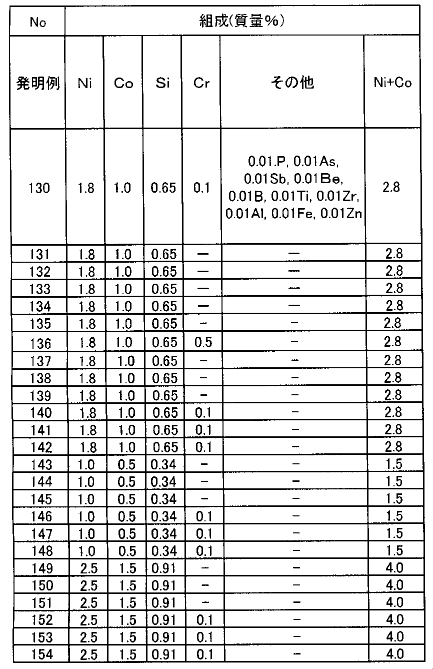


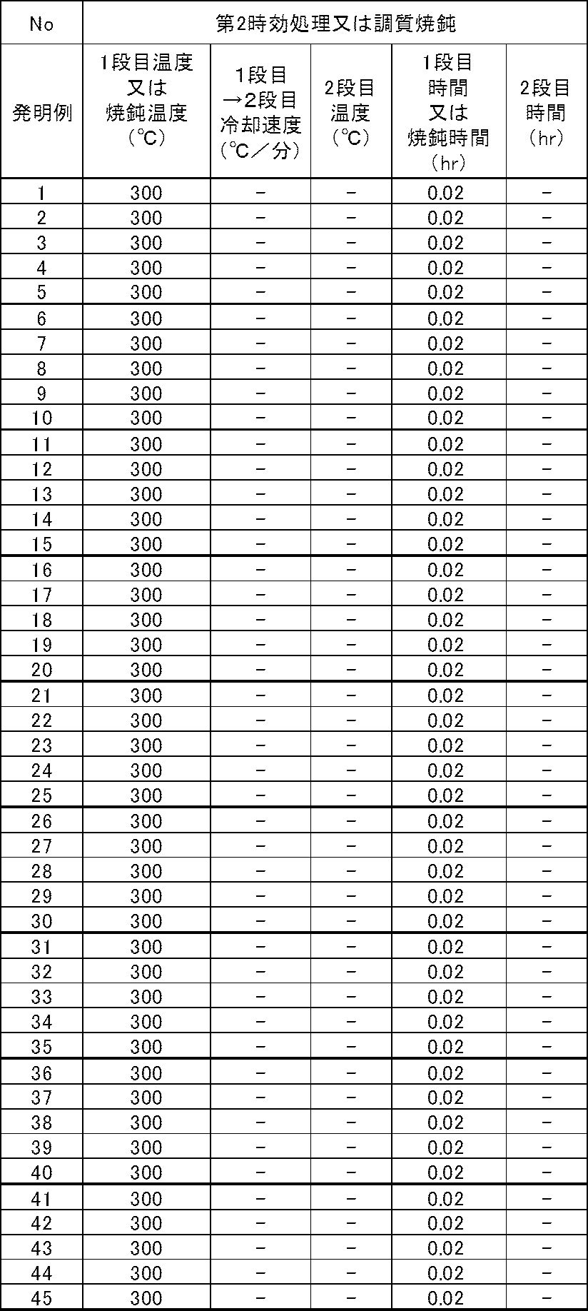
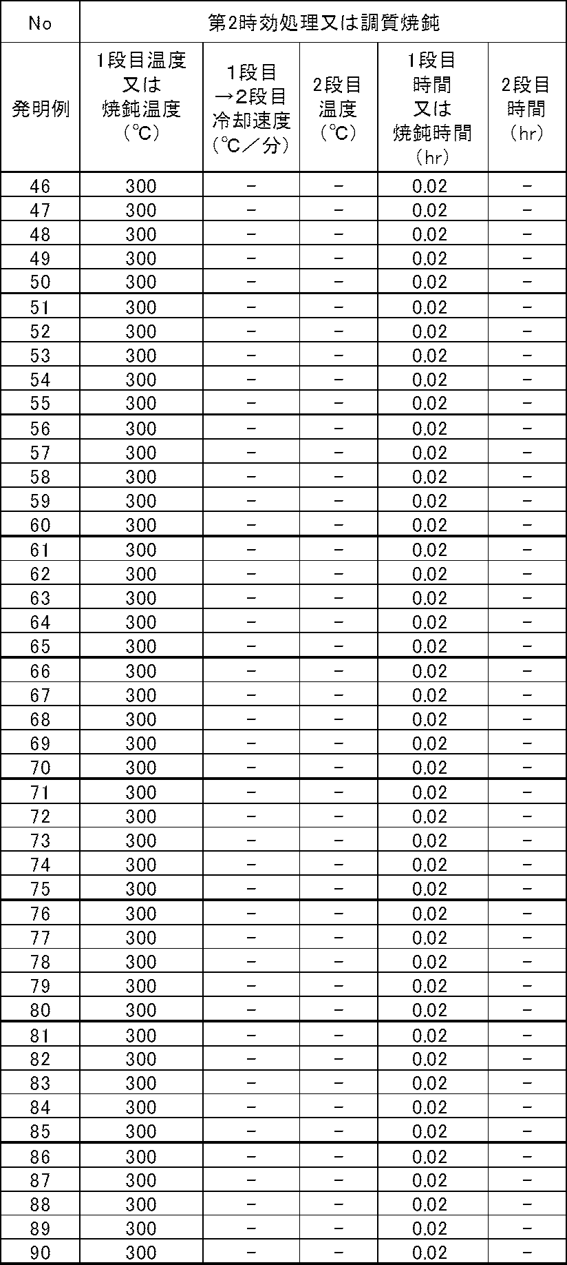

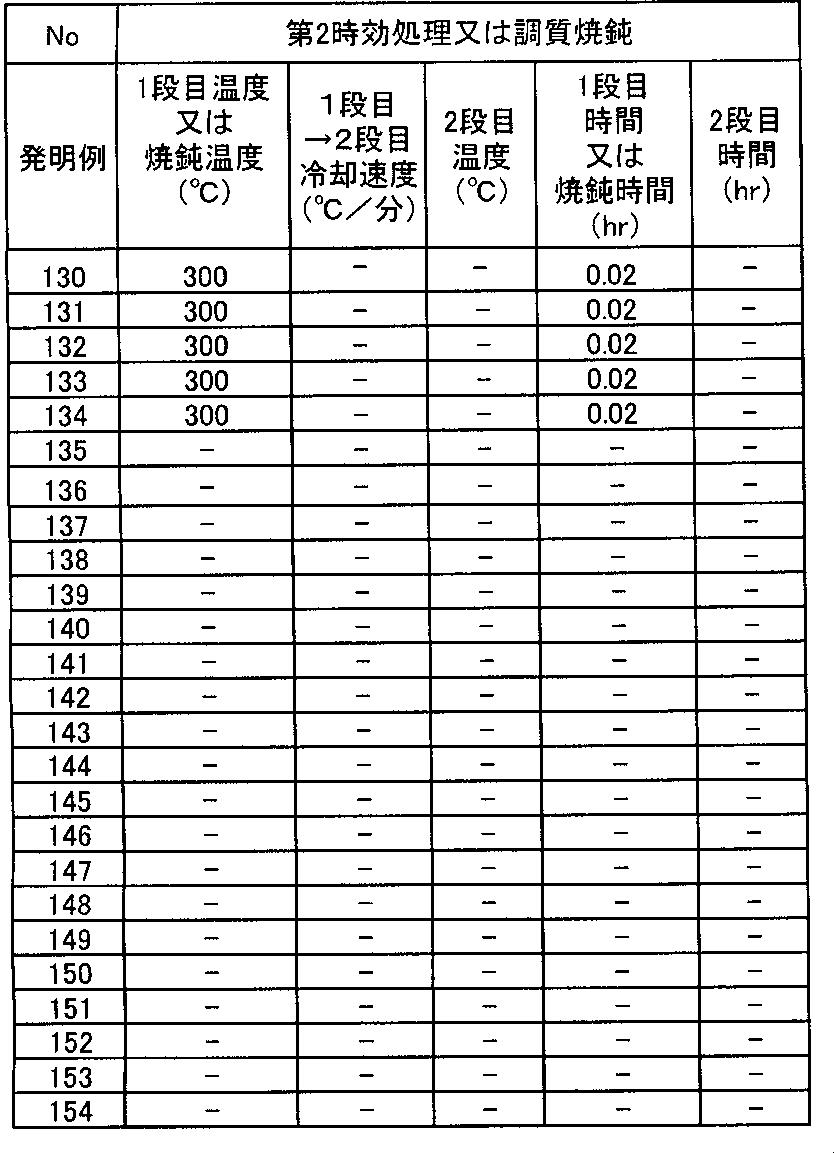


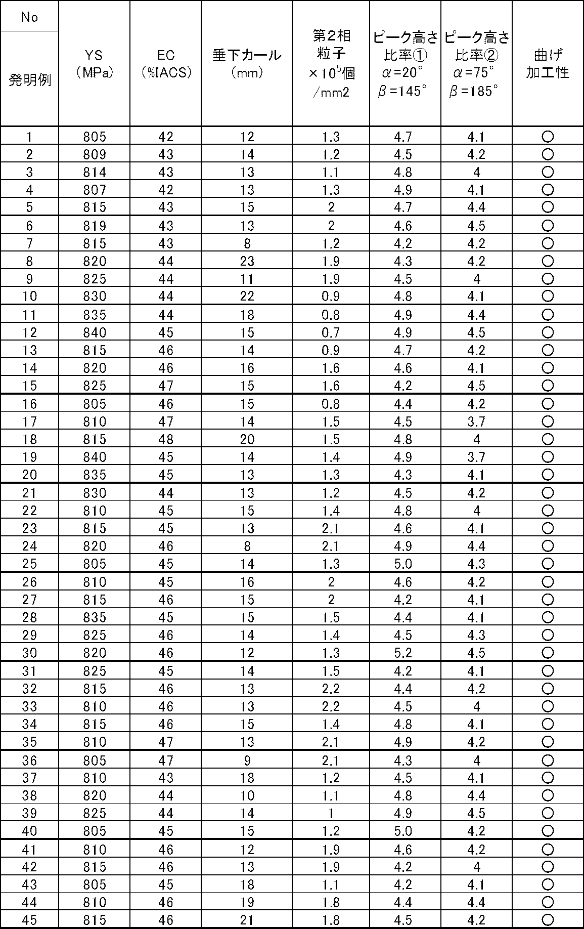


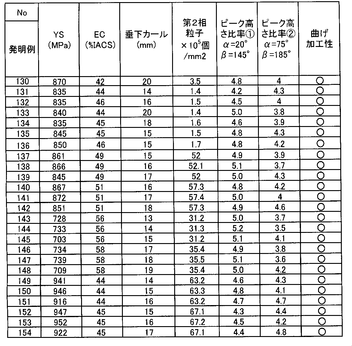

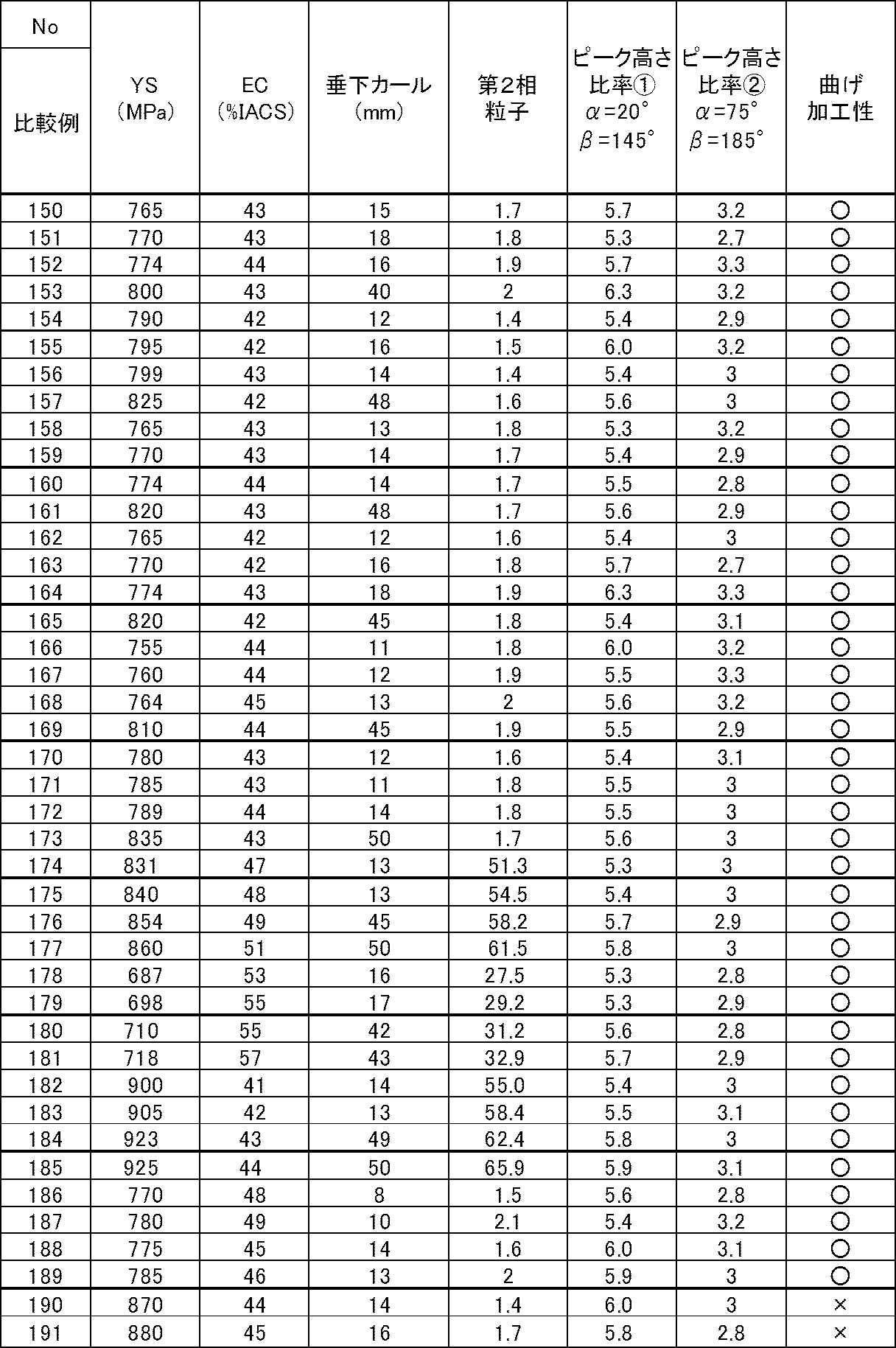
発明例No.1~154は、「α=20°におけるβ角度145°のピーク高さ比率」が5.2倍以下であり、「α=75°におけるβ角度185°のピーク高さ比率」が3.4倍以上であり、強度及び導電率のバランスに優れ、しかも、垂下カールが抑制されていることが分かる。更に、曲げ加工性も優れていることが分かる。また、溶体化処理後の冷却条件を好ましい条件に変更した発明例No.137~154では、母相中に析出した第二相粒子のうち、粒径が0.1μm以上1μm以下のものの個数密度が5×10⁵~1×10⁷個/mm2の範囲にあり、より優れた特性のバランスを達成した。
比較例No.7~12、65~70、174、175、178、179、182、183は、第一の時効を1段時効で行った例である。
比較例No.1~6、13、59~64、71、129、133、137、141、145、149、153、157、161、165、169、173、176、177、180、181、184、185は第一の時効を2段時効で行った例である。
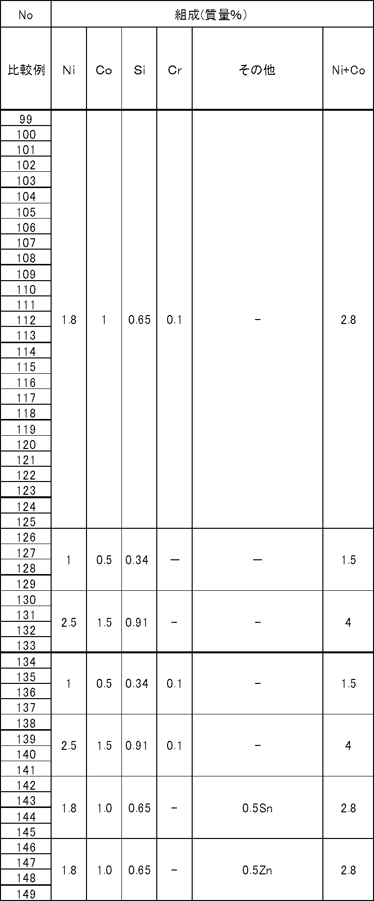
比較例No.14~58、72~116、126~128、130~132、134~136、138~140、142~144、146~148、150~152、154~156、158~160、162~164、166~168、170~172は3段目の時効時間が短かった例である。
比較例No.117~119は3段目の時効温度が低かった例である。
比較例No.120~122は3段目の時効温度が高かった例である。
比較例No.123~125は3段目の時効時間が長かった例である。
比較例No.186及び187は1段目から2段目、2段目から3段目への冷却速度が高すぎた例である。
比較例No.188及び189は1段目から2段目、2段目から3段目への冷却速度が低すぎた例である。
比較例No.190及び191は第1の時効処理後に冷間圧延を実施するまでは発明例の工程と同じであるが、その後に第二の時効処理及び冷間圧延を行った例である。
比較例No.13、71、129、133、137、141、145、149、153、157、161、165、169、173、176、177、180、181、184、185、190、191においては第二の時効処理も実施した。
比較例は何れも「α=20°におけるβ角度145°のピーク高さ比率」が5.2倍を超え、「α=75°におけるβ角度185°のピーク高さ比率」が3.4倍未満であり、発明例に比べて強度、導電性及び垂下カールのバランスに劣っていることが分かる。
図1より、Crを添加しない発明例では、式ア:-11×([Ni]+[Co])2+146×([Ni]+[Co])+564≧YS≧-21×([Ni]+[Co])2+202×([Ni]+[Co])+436の関係を満たすことが分かる。
図2より、Crを添加した発明例では、式イ:-14×([Ni]+[Co])2+164×([Ni]+[Co])+551≧YS≧-22×([Ni]+[Co])2+204×([Ni]+[Co])+447の関係を満たすことが分かる。
図3より、Crを添加しない発明例では、式ウ:-0.0563×〔YS〕+94.1972≦EC≦-0.0563×〔YS〕+98.7040の関係を満たすことが分かる。
図4より、Crを添加した発明例では、式エ:-0.0610×〔YS〕+99.7465≦EC≦-0.0610×〔YS〕+104.6291の関係を満たすことが分かる。
Claims (14)
- Ni:1.0~2.5質量%、Co:0.5~2.5質量%、Si:0.3~1.2質量%を含有し、残部がCu及び不可避不純物からなる電子材料用銅合金条であって、圧延面を基準としたX線回折極点図測定により得られる結果で、下記の(a)及び(b)の両方を満たす銅合金条:
(a){200}極点図においてα=20°におけるβ走査による回折ピーク強度のうち、β角度145°のピーク高さが標準銅粉末のそれに対して5.2倍以下であること;
(b){111}極点図においてα=75°におけるβ走査による回折ピーク強度のうち、β角度185°のピーク高さが標準銅粉末のそれに対して3.4倍以上であること。 - 圧延方向に平行な方向における垂下カールが35mm以下である請求項1に記載の銅合金条。
- Niの含有量(質量%)を[Ni]、Coの含有量(質量%)を[Co]、0.2%耐力をYS(MPa)としたときに、
式ア:-11×([Ni]+[Co])2+146×([Ni]+[Co])+564≧YS≧-21×([Ni]+[Co])2+202×([Ni]+[Co])+436
を満たす請求項1又は2に記載の銅合金条。 - 0.2%耐力をYS(MPa)、導電率をEC(%IACS)としたときに、
673≦YS≦976、42.5≦EC≦57.5、式ウ:-0.0563×〔YS〕+94.1972≦EC≦-0.0563×〔YS〕+98.7040
を満たす請求項1~3の何れか一項に記載の銅合金条。 - 母相中に析出した第二相粒子のうち、粒径が0.1μm以上1μm以下のものの個数密度が5×10⁵~1×10⁷個/mm2である請求項1~4の何れか一項に記載の銅合金条。
- 更にCr:0.03~0.5質量%を含有する請求項1、2又は5に記載の銅合金条。
- Niの含有量(質量%)を[Ni]、Coの含有量(質量%)を[Co]、0.2%耐力をYS(MPa)としたときに、
式イ:-14×([Ni]+[Co])2+164×([Ni]+[Co])+551≧YS≧-22×([Ni]+[Co])2+204×([Ni]+[Co])+447
を満たす請求項6に記載の銅合金条。 - 0.2%耐力をYS(MPa)、導電率をEC(%IACS)としたときに、
679≦YS≦982、43.5≦EC≦59.5、式エ:-0.0610×〔YS〕+99.7465≦EC≦-0.0610×〔YS〕+104.6291
を満たす請求項6又は7に記載の銅合金条。 - 更にMg、P、As、Sb、Be、B、Mn、Sn、Ti、Zr、Al、Fe、Zn及びAgの群から選ばれる少なくとも1種を総計で最大2.0質量%含有する請求項1~8何れか一項記載の銅合金条。
- -以下の(1)~(3)から選ばれる組成をもつインゴットを溶解鋳造する工程1と、
(1)Ni:1.0~2.5質量%、Co:0.5~2.5質量%、Si:0.3~1.2質量%を含有し、残部がCu及び不可避不純物からなる組成
(2)Ni:1.0~2.5質量%、Co:0.5~2.5質量%、Si:0.3~1.2質量%、Cr:0.03~0.5質量%を含有し、残部がCu及び不可避不純物からなる組成
(3)(1)又は(2)に、更にMg、P、As、Sb、Be、B、Mn、Sn、Ti、Zr、Al、Fe、Zn及びAgの群から選ばれる少なくとも1種を総計で最大2.0質量%含有する組成
-950℃以上1050℃以下で1時間以上加熱後に熱間圧延を行い、熱間圧延終了時の温度を850℃以上とし、850℃から400℃までの平均冷却速度を15℃/s以上として冷却する工程2と、
-冷間圧延工程3と、
-850℃以上1050℃以下で溶体化処理を行い、400℃までの平均冷却速度を毎秒10℃以上として冷却する工程4と、
-材料温度を400~500℃として1~12時間加熱する一段目と、次いで、材料温度を350~450℃として1~12時間加熱する二段目と、次いで、材料温度を260~340℃として4~30時間加熱する三段目を有し、一段目から二段目までの冷却速度及び二段目から三段目までの冷却速度はそれぞれ1~8℃/分とし、一段目と二段目の温度差を20~60℃とし、二段目と三段目の温度差を20~180℃としてバッチ炉で材料をコイル状に巻いたまま多段時効する時効処理工程5と、
-冷間圧延工程6と、
を順に行うことを含む請求項1~9の何れか一項に記載の銅合金条の製造方法。 - 工程6の後に、材料温度を200~500℃として1秒~1000秒加熱する調質焼鈍を実施する請求項10に記載の製造方法。
- 工程4における溶体化処理は、400℃までの平均冷却速度を毎秒10℃以上として冷却する条件に替えて、材料温度が650℃に低下するまでの平均冷却速度を1℃/s以上15℃/s未満として冷却し、650℃から400℃まで低下するときの平均冷却速度を15℃/s以上として冷却する請求項10又は11に記載の製造方法。
- 請求項1~9の何れか一項に記載の銅合金条を加工して得られた伸銅品。
- 請求項1~9の何れか一項に記載の銅合金条を加工して得られた電子部品。
Priority Applications (4)
| Application Number | Priority Date | Filing Date | Title |
|---|---|---|---|
| EP11848621.6A EP2641983A4 (en) | 2010-12-13 | 2011-11-11 | COUPLER ALLOY ON CU-NI-SI-CO BASE FOR ELECTRONIC MATERIAL AND METHOD OF MANUFACTURING THEREOF |
| US13/993,648 US9401230B2 (en) | 2010-12-13 | 2011-11-11 | Cu-Ni-Si-Co copper alloy for electronic materials and manufacturing method thereof |
| KR1020137013304A KR20130109161A (ko) | 2010-12-13 | 2011-11-11 | 전자 재료용 Cu-Ni-Si-Co 계 구리 합금 및 그 제조 방법 |
| CN201180059363.7A CN103249851B (zh) | 2010-12-13 | 2011-11-11 | 电子材料用Cu-Ni-Si-Co系铜合金及其制造方法 |
Applications Claiming Priority (2)
| Application Number | Priority Date | Filing Date | Title |
|---|---|---|---|
| JP2010277279A JP5441876B2 (ja) | 2010-12-13 | 2010-12-13 | 電子材料用Cu−Ni−Si−Co系銅合金及びその製造方法 |
| JP2010-277279 | 2010-12-13 |
Publications (1)
| Publication Number | Publication Date |
|---|---|
| WO2012081342A1 true WO2012081342A1 (ja) | 2012-06-21 |
Family
ID=46244455
Family Applications (1)
| Application Number | Title | Priority Date | Filing Date |
|---|---|---|---|
| PCT/JP2011/076082 WO2012081342A1 (ja) | 2010-12-13 | 2011-11-11 | 電子材料用Cu-Ni-Si-Co系銅合金及びその製造方法 |
Country Status (7)
| Country | Link |
|---|---|
| US (1) | US9401230B2 (ja) |
| EP (1) | EP2641983A4 (ja) |
| JP (1) | JP5441876B2 (ja) |
| KR (1) | KR20130109161A (ja) |
| CN (1) | CN103249851B (ja) |
| TW (1) | TWI447240B (ja) |
| WO (1) | WO2012081342A1 (ja) |
Cited By (2)
| Publication number | Priority date | Publication date | Assignee | Title |
|---|---|---|---|---|
| KR20140056003A (ko) * | 2012-10-31 | 2014-05-09 | 도와 메탈테크 가부시키가이샤 | Cu-Ni-Co-Sⅰ계 구리 합금 판재 및 이의 제조법 |
| JP2021046590A (ja) * | 2019-09-19 | 2021-03-25 | Jx金属株式会社 | 銅合金、伸銅品及び電子機器部品 |
Families Citing this family (16)
| Publication number | Priority date | Publication date | Assignee | Title |
|---|---|---|---|---|
| JP4677505B1 (ja) * | 2010-03-31 | 2011-04-27 | Jx日鉱日石金属株式会社 | 電子材料用Cu−Ni−Si−Co系銅合金及びその製造方法 |
| JP5451674B2 (ja) * | 2011-03-28 | 2014-03-26 | Jx日鉱日石金属株式会社 | 電子材料用Cu−Si−Co系銅合金及びその製造方法 |
| JP4799701B1 (ja) * | 2011-03-29 | 2011-10-26 | Jx日鉱日石金属株式会社 | 電子材料用Cu−Co−Si系銅合金条及びその製造方法 |
| JP5623960B2 (ja) * | 2011-03-30 | 2014-11-12 | Jx日鉱日石金属株式会社 | 電子材料用Cu−Ni−Si系銅合金条及びその製造方法 |
| KR101274063B1 (ko) * | 2013-01-22 | 2013-06-12 | 한국기계연구원 | 배향된 석출물을 가지는 금속복합재료 및 이의 제조방법 |
| JP6366298B2 (ja) * | 2014-02-28 | 2018-08-01 | Dowaメタルテック株式会社 | 高強度銅合金薄板材およびその製造方法 |
| JP6573503B2 (ja) * | 2015-08-24 | 2019-09-11 | Dowaメタルテック株式会社 | Cu−Ni−Co−Si系高強度銅合金薄板材およびその製造方法並びに導電ばね部材 |
| WO2017168803A1 (ja) | 2016-03-31 | 2017-10-05 | Dowaメタルテック株式会社 | Cu-Ni-Si系銅合金板材および製造法 |
| JP6385383B2 (ja) * | 2016-03-31 | 2018-09-05 | Jx金属株式会社 | 銅合金板材および銅合金板材の製造方法 |
| US10648067B2 (en) * | 2016-12-15 | 2020-05-12 | Materion Corporation | Precipitation strengthened metal alloy article |
| CN108927518A (zh) * | 2018-07-31 | 2018-12-04 | 西安理工大学 | 快速制备Cu-Ni-Si合金薄板的直接粉末轧制方法 |
| CN112680627B (zh) * | 2020-12-21 | 2022-05-13 | 无锡天宝电机有限公司 | 一种转子导条及其制备方法 |
| CN112921257B (zh) * | 2021-01-25 | 2022-02-01 | 安德伦(重庆)材料科技有限公司 | 一种无铍高强度铜合金零件的热处理方法及其成形方法 |
| JP7538775B2 (ja) * | 2021-05-27 | 2024-08-22 | 日本碍子株式会社 | 銅合金 |
| KR102405236B1 (ko) * | 2022-05-11 | 2022-06-07 | 고려아연 주식회사 | 전해 동박의 제조방법 |
| CN115094258B (zh) * | 2022-07-13 | 2023-02-17 | 浙江惟精新材料股份有限公司 | 一种高强高塑高折弯Cu-Ni-Si-Co合金及其制备方法和应用 |
Citations (4)
| Publication number | Priority date | Publication date | Assignee | Title |
|---|---|---|---|---|
| JP2008013836A (ja) * | 2006-07-10 | 2008-01-24 | Dowa Holdings Co Ltd | 異方性の少ない高強度銅合金板材およびその製造法 |
| JP2009242890A (ja) * | 2008-03-31 | 2009-10-22 | Nippon Mining & Metals Co Ltd | 電子材料用Cu−Ni−Si−Co系銅合金及びその製造方法 |
| JP2009242921A (ja) * | 2008-03-31 | 2009-10-22 | Nippon Mining & Metals Co Ltd | 電子材料用Cu−Ni−Si−Co−Cr系合金 |
| JP2010215976A (ja) * | 2009-03-17 | 2010-09-30 | Furukawa Electric Co Ltd:The | 銅合金板材 |
Family Cites Families (12)
| Publication number | Priority date | Publication date | Assignee | Title |
|---|---|---|---|---|
| US7182823B2 (en) | 2002-07-05 | 2007-02-27 | Olin Corporation | Copper alloy containing cobalt, nickel and silicon |
| CA2559103A1 (en) * | 2004-03-12 | 2005-09-22 | Sumitomo Metal Industries, Ltd. | Copper alloy and method for production thereof |
| JP4809602B2 (ja) * | 2004-05-27 | 2011-11-09 | 古河電気工業株式会社 | 銅合金 |
| JP2006097113A (ja) * | 2004-09-30 | 2006-04-13 | Nippon Mining & Metals Co Ltd | 析出硬化型銅合金の製造方法、析出硬化型銅合金及び伸銅品 |
| JP4566048B2 (ja) | 2005-03-31 | 2010-10-20 | 株式会社神戸製鋼所 | 曲げ加工性に優れた高強度銅合金板及びその製造方法 |
| JP4937815B2 (ja) * | 2007-03-30 | 2012-05-23 | Jx日鉱日石金属株式会社 | 電子材料用Cu−Ni−Si−Co系銅合金及びその製造方法 |
| JP4981748B2 (ja) * | 2007-05-31 | 2012-07-25 | 古河電気工業株式会社 | 電気・電子機器用銅合金 |
| WO2010064547A1 (ja) * | 2008-12-01 | 2010-06-10 | 日鉱金属株式会社 | 電子材料用Cu-Ni-Si-Co系銅合金及びその製造方法 |
| JP4930527B2 (ja) * | 2009-03-05 | 2012-05-16 | 日立電線株式会社 | 銅合金材及び銅合金材の製造方法 |
| JP4677505B1 (ja) * | 2010-03-31 | 2011-04-27 | Jx日鉱日石金属株式会社 | 電子材料用Cu−Ni−Si−Co系銅合金及びその製造方法 |
| JP5451674B2 (ja) * | 2011-03-28 | 2014-03-26 | Jx日鉱日石金属株式会社 | 電子材料用Cu−Si−Co系銅合金及びその製造方法 |
| JP4799701B1 (ja) * | 2011-03-29 | 2011-10-26 | Jx日鉱日石金属株式会社 | 電子材料用Cu−Co−Si系銅合金条及びその製造方法 |
-
2010
- 2010-12-13 JP JP2010277279A patent/JP5441876B2/ja active Active
-
2011
- 2011-11-11 WO PCT/JP2011/076082 patent/WO2012081342A1/ja active Application Filing
- 2011-11-11 EP EP11848621.6A patent/EP2641983A4/en not_active Withdrawn
- 2011-11-11 KR KR1020137013304A patent/KR20130109161A/ko not_active Application Discontinuation
- 2011-11-11 CN CN201180059363.7A patent/CN103249851B/zh active Active
- 2011-11-11 US US13/993,648 patent/US9401230B2/en active Active
- 2011-11-29 TW TW100143686A patent/TWI447240B/zh active
Patent Citations (4)
| Publication number | Priority date | Publication date | Assignee | Title |
|---|---|---|---|---|
| JP2008013836A (ja) * | 2006-07-10 | 2008-01-24 | Dowa Holdings Co Ltd | 異方性の少ない高強度銅合金板材およびその製造法 |
| JP2009242890A (ja) * | 2008-03-31 | 2009-10-22 | Nippon Mining & Metals Co Ltd | 電子材料用Cu−Ni−Si−Co系銅合金及びその製造方法 |
| JP2009242921A (ja) * | 2008-03-31 | 2009-10-22 | Nippon Mining & Metals Co Ltd | 電子材料用Cu−Ni−Si−Co−Cr系合金 |
| JP2010215976A (ja) * | 2009-03-17 | 2010-09-30 | Furukawa Electric Co Ltd:The | 銅合金板材 |
Non-Patent Citations (1)
| Title |
|---|
| See also references of EP2641983A4 * |
Cited By (5)
| Publication number | Priority date | Publication date | Assignee | Title |
|---|---|---|---|---|
| KR20140056003A (ko) * | 2012-10-31 | 2014-05-09 | 도와 메탈테크 가부시키가이샤 | Cu-Ni-Co-Sⅰ계 구리 합금 판재 및 이의 제조법 |
| EP2728025A3 (en) * | 2012-10-31 | 2017-11-01 | Dowa Metaltech Co., Ltd. | Cu-Ni-Co-Si based copper alloy sheet material and method for producing the same |
| KR102222540B1 (ko) * | 2012-10-31 | 2021-03-05 | 도와 메탈테크 가부시키가이샤 | Cu-Ni-Co-Sⅰ계 구리 합금 판재 및 이의 제조법 |
| JP2021046590A (ja) * | 2019-09-19 | 2021-03-25 | Jx金属株式会社 | 銅合金、伸銅品及び電子機器部品 |
| JP7430502B2 (ja) | 2019-09-19 | 2024-02-13 | Jx金属株式会社 | 銅合金線材及び電子機器部品 |
Also Published As
| Publication number | Publication date |
|---|---|
| US9401230B2 (en) | 2016-07-26 |
| EP2641983A1 (en) | 2013-09-25 |
| US20130263978A1 (en) | 2013-10-10 |
| EP2641983A4 (en) | 2016-04-13 |
| JP5441876B2 (ja) | 2014-03-12 |
| TWI447240B (zh) | 2014-08-01 |
| TW201229256A (en) | 2012-07-16 |
| JP2012126934A (ja) | 2012-07-05 |
| CN103249851B (zh) | 2015-06-17 |
| CN103249851A (zh) | 2013-08-14 |
| KR20130109161A (ko) | 2013-10-07 |
Similar Documents
| Publication | Publication Date | Title |
|---|---|---|
| JP5441876B2 (ja) | 電子材料用Cu−Ni−Si−Co系銅合金及びその製造方法 | |
| JP4677505B1 (ja) | 電子材料用Cu−Ni−Si−Co系銅合金及びその製造方法 | |
| JP4799701B1 (ja) | 電子材料用Cu−Co−Si系銅合金条及びその製造方法 | |
| JP4937815B2 (ja) | 電子材料用Cu−Ni−Si−Co系銅合金及びその製造方法 | |
| JP4837697B2 (ja) | 電子材料用Cu−Ni−Si−Co系銅合金及びその製造方法 | |
| JP5506806B2 (ja) | 電子材料用Cu−Ni−Si−Co系銅合金及びその製造方法 | |
| JP5451674B2 (ja) | 電子材料用Cu−Si−Co系銅合金及びその製造方法 | |
| WO2009122869A1 (ja) | 電子材料用Cu-Ni-Si-Co系銅合金及びその製造方法 | |
| JP4708485B2 (ja) | 電子材料用Cu−Co−Si系銅合金及びその製造方法 | |
| WO2012043170A1 (ja) | 電子材料用Cu-Co-Si系銅合金及びその製造方法 | |
| WO2012026488A1 (ja) | 電子材料用Cu-Co-Si系合金 | |
| JP2012193408A (ja) | 曲げ加工性に優れたCu−Ni−Si系合金 | |
| JP6222885B2 (ja) | 電子材料用Cu−Ni−Si−Co系銅合金 | |
| JP2012229467A (ja) | 電子材料用Cu−Ni−Si系銅合金 | |
| JP5524901B2 (ja) | 電子材料用Cu−Ni−Si−Co系銅合金 | |
| JP5623960B2 (ja) | 電子材料用Cu−Ni−Si系銅合金条及びその製造方法 | |
| JP2012229469A (ja) | 電子材料用Cu−Si−Co系銅合金及びその製造方法 | |
| JP2016183418A (ja) | 電子材料用Cu−Ni−Si−Co系銅合金 | |
| JP5595961B2 (ja) | 電子材料用Cu−Ni−Si系銅合金及びその製造方法 | |
| TWI391952B (zh) | Cu-Ni-Si-Co based copper alloy for electronic materials and its manufacturing method | |
| JP2012046804A (ja) | 銅合金材料及びその製造方法 |
Legal Events
| Date | Code | Title | Description |
|---|---|---|---|
| 121 | Ep: the epo has been informed by wipo that ep was designated in this application |
Ref document number: 11848621 Country of ref document: EP Kind code of ref document: A1 |
|
| ENP | Entry into the national phase |
Ref document number: 20137013304 Country of ref document: KR Kind code of ref document: A |
|
| WWE | Wipo information: entry into national phase |
Ref document number: 13993648 Country of ref document: US |
|
| NENP | Non-entry into the national phase |
Ref country code: DE |
|
| REEP | Request for entry into the european phase |
Ref document number: 2011848621 Country of ref document: EP |
|
| WWE | Wipo information: entry into national phase |
Ref document number: 2011848621 Country of ref document: EP |