WO2012077520A1 - 有機電界発光素子 - Google Patents
有機電界発光素子 Download PDFInfo
- Publication number
- WO2012077520A1 WO2012077520A1 PCT/JP2011/077384 JP2011077384W WO2012077520A1 WO 2012077520 A1 WO2012077520 A1 WO 2012077520A1 JP 2011077384 W JP2011077384 W JP 2011077384W WO 2012077520 A1 WO2012077520 A1 WO 2012077520A1
- Authority
- WO
- WIPO (PCT)
- Prior art keywords
- organic
- compound
- group
- general formula
- integer
- Prior art date
Links
- PNRYFGZXGQIDRU-UHFFFAOYSA-N C[n](c1ccc2)c(C=C[I]=C3)c3c1c2-[n]1c(C=C[Cl]=C2)c2c2c1cccc2 Chemical compound C[n](c1ccc2)c(C=C[I]=C3)c3c1c2-[n]1c(C=C[Cl]=C2)c2c2c1cccc2 PNRYFGZXGQIDRU-UHFFFAOYSA-N 0.000 description 1
- KLTYBOPLZHUAHX-UHFFFAOYSA-N c(cc1)cc(c2c3cccc2)c1[n]3-c1c(c2ccccc2[n]2-c3cc(-[n](c4ccccc44)c5c4c(-[n]4c6ccccc6c6c4cccc6)ccc5)nc(-[n]4c5cccc(-[n]6c(cccc7)c7c7ccccc67)c5c5ccccc45)c3)c2ccc1 Chemical compound c(cc1)cc(c2c3cccc2)c1[n]3-c1c(c2ccccc2[n]2-c3cc(-[n](c4ccccc44)c5c4c(-[n]4c6ccccc6c6c4cccc6)ccc5)nc(-[n]4c5cccc(-[n]6c(cccc7)c7c7ccccc67)c5c5ccccc45)c3)c2ccc1 KLTYBOPLZHUAHX-UHFFFAOYSA-N 0.000 description 1
- IVHHVFWRNFJAFC-UHFFFAOYSA-N c(cc1)cc(c2c3cccc2)c1[n]3-c1cccc2c1c(cccc1)c1[n]2-c1cc(-c2cc(-c3cccc(-[n]4c5cccc(-[n]6c7ccccc7c7c6cccc7)c5c5c4cccc5)c3)cc(-c3cccc(-[n]4c5cccc(-[n]6c7ccccc7c7ccccc67)c5c5ccccc45)c3)c2)ccc1 Chemical compound c(cc1)cc(c2c3cccc2)c1[n]3-c1cccc2c1c(cccc1)c1[n]2-c1cc(-c2cc(-c3cccc(-[n]4c5cccc(-[n]6c7ccccc7c7c6cccc7)c5c5c4cccc5)c3)cc(-c3cccc(-[n]4c5cccc(-[n]6c7ccccc7c7ccccc67)c5c5ccccc45)c3)c2)ccc1 IVHHVFWRNFJAFC-UHFFFAOYSA-N 0.000 description 1
- KXNGLDFKLQBGCG-UHFFFAOYSA-N c(cc1)cc(c2ccccc22)c1[n]2-c1cccc2c1c1ccccc1[n]2-c1cc(-[n]2c3cccc(-[n]4c5ccccc5c5c4cccc5)c3c3c2cccc3)nc(-[n]2c3cccc(-[n]4c(cccc5)c5c5c4cccc5)c3c3c2cccc3)n1 Chemical compound c(cc1)cc(c2ccccc22)c1[n]2-c1cccc2c1c1ccccc1[n]2-c1cc(-[n]2c3cccc(-[n]4c5ccccc5c5c4cccc5)c3c3c2cccc3)nc(-[n]2c3cccc(-[n]4c(cccc5)c5c5c4cccc5)c3c3c2cccc3)n1 KXNGLDFKLQBGCG-UHFFFAOYSA-N 0.000 description 1
- OQNCCQGQEGMYDZ-UHFFFAOYSA-N c(cc1)cc(c2ccccc22)c1[n]2-c1cccc2c1c1ccccc1[n]2C(N1)N=C([n]2c3cccc(-[n]4c(cccc5)c5c5c4cccc5)c3c3c2cccc3)N=C1[n]1c2cccc(-[n]3c4ccccc4c4c3cccc4)c2c2ccccc12 Chemical compound c(cc1)cc(c2ccccc22)c1[n]2-c1cccc2c1c1ccccc1[n]2C(N1)N=C([n]2c3cccc(-[n]4c(cccc5)c5c5c4cccc5)c3c3c2cccc3)N=C1[n]1c2cccc(-[n]3c4ccccc4c4c3cccc4)c2c2ccccc12 OQNCCQGQEGMYDZ-UHFFFAOYSA-N 0.000 description 1
Images


Classifications
-
- H—ELECTRICITY
- H10—SEMICONDUCTOR DEVICES; ELECTRIC SOLID-STATE DEVICES NOT OTHERWISE PROVIDED FOR
- H10K—ORGANIC ELECTRIC SOLID-STATE DEVICES
- H10K85/00—Organic materials used in the body or electrodes of devices covered by this subclass
- H10K85/60—Organic compounds having low molecular weight
- H10K85/649—Aromatic compounds comprising a hetero atom
- H10K85/657—Polycyclic condensed heteroaromatic hydrocarbons
- H10K85/6572—Polycyclic condensed heteroaromatic hydrocarbons comprising only nitrogen in the heteroaromatic polycondensed ring system, e.g. phenanthroline or carbazole
-
- C—CHEMISTRY; METALLURGY
- C07—ORGANIC CHEMISTRY
- C07D—HETEROCYCLIC COMPOUNDS
- C07D209/00—Heterocyclic compounds containing five-membered rings, condensed with other rings, with one nitrogen atom as the only ring hetero atom
- C07D209/56—Ring systems containing three or more rings
- C07D209/80—[b, c]- or [b, d]-condensed
- C07D209/82—Carbazoles; Hydrogenated carbazoles
-
- C—CHEMISTRY; METALLURGY
- C07—ORGANIC CHEMISTRY
- C07D—HETEROCYCLIC COMPOUNDS
- C07D401/00—Heterocyclic compounds containing two or more hetero rings, having nitrogen atoms as the only ring hetero atoms, at least one ring being a six-membered ring with only one nitrogen atom
- C07D401/02—Heterocyclic compounds containing two or more hetero rings, having nitrogen atoms as the only ring hetero atoms, at least one ring being a six-membered ring with only one nitrogen atom containing two hetero rings
- C07D401/04—Heterocyclic compounds containing two or more hetero rings, having nitrogen atoms as the only ring hetero atoms, at least one ring being a six-membered ring with only one nitrogen atom containing two hetero rings directly linked by a ring-member-to-ring-member bond
-
- C—CHEMISTRY; METALLURGY
- C07—ORGANIC CHEMISTRY
- C07D—HETEROCYCLIC COMPOUNDS
- C07D403/00—Heterocyclic compounds containing two or more hetero rings, having nitrogen atoms as the only ring hetero atoms, not provided for by group C07D401/00
- C07D403/02—Heterocyclic compounds containing two or more hetero rings, having nitrogen atoms as the only ring hetero atoms, not provided for by group C07D401/00 containing two hetero rings
- C07D403/04—Heterocyclic compounds containing two or more hetero rings, having nitrogen atoms as the only ring hetero atoms, not provided for by group C07D401/00 containing two hetero rings directly linked by a ring-member-to-ring-member bond
-
- C—CHEMISTRY; METALLURGY
- C07—ORGANIC CHEMISTRY
- C07D—HETEROCYCLIC COMPOUNDS
- C07D405/00—Heterocyclic compounds containing both one or more hetero rings having oxygen atoms as the only ring hetero atoms, and one or more rings having nitrogen as the only ring hetero atom
- C07D405/02—Heterocyclic compounds containing both one or more hetero rings having oxygen atoms as the only ring hetero atoms, and one or more rings having nitrogen as the only ring hetero atom containing two hetero rings
- C07D405/04—Heterocyclic compounds containing both one or more hetero rings having oxygen atoms as the only ring hetero atoms, and one or more rings having nitrogen as the only ring hetero atom containing two hetero rings directly linked by a ring-member-to-ring-member bond
-
- C—CHEMISTRY; METALLURGY
- C07—ORGANIC CHEMISTRY
- C07D—HETEROCYCLIC COMPOUNDS
- C07D409/00—Heterocyclic compounds containing two or more hetero rings, at least one ring having sulfur atoms as the only ring hetero atoms
- C07D409/02—Heterocyclic compounds containing two or more hetero rings, at least one ring having sulfur atoms as the only ring hetero atoms containing two hetero rings
- C07D409/04—Heterocyclic compounds containing two or more hetero rings, at least one ring having sulfur atoms as the only ring hetero atoms containing two hetero rings directly linked by a ring-member-to-ring-member bond
-
- C—CHEMISTRY; METALLURGY
- C09—DYES; PAINTS; POLISHES; NATURAL RESINS; ADHESIVES; COMPOSITIONS NOT OTHERWISE PROVIDED FOR; APPLICATIONS OF MATERIALS NOT OTHERWISE PROVIDED FOR
- C09K—MATERIALS FOR MISCELLANEOUS APPLICATIONS, NOT PROVIDED FOR ELSEWHERE
- C09K11/00—Luminescent, e.g. electroluminescent, chemiluminescent materials
- C09K11/06—Luminescent, e.g. electroluminescent, chemiluminescent materials containing organic luminescent materials
-
- H—ELECTRICITY
- H05—ELECTRIC TECHNIQUES NOT OTHERWISE PROVIDED FOR
- H05B—ELECTRIC HEATING; ELECTRIC LIGHT SOURCES NOT OTHERWISE PROVIDED FOR; CIRCUIT ARRANGEMENTS FOR ELECTRIC LIGHT SOURCES, IN GENERAL
- H05B33/00—Electroluminescent light sources
- H05B33/12—Light sources with substantially two-dimensional radiating surfaces
- H05B33/14—Light sources with substantially two-dimensional radiating surfaces characterised by the chemical or physical composition or the arrangement of the electroluminescent material, or by the simultaneous addition of the electroluminescent material in or onto the light source
-
- H—ELECTRICITY
- H10—SEMICONDUCTOR DEVICES; ELECTRIC SOLID-STATE DEVICES NOT OTHERWISE PROVIDED FOR
- H10K—ORGANIC ELECTRIC SOLID-STATE DEVICES
- H10K30/00—Organic devices sensitive to infrared radiation, light, electromagnetic radiation of shorter wavelength or corpuscular radiation
- H10K30/80—Constructional details
- H10K30/865—Intermediate layers comprising a mixture of materials of the adjoining active layers
-
- H—ELECTRICITY
- H10—SEMICONDUCTOR DEVICES; ELECTRIC SOLID-STATE DEVICES NOT OTHERWISE PROVIDED FOR
- H10K—ORGANIC ELECTRIC SOLID-STATE DEVICES
- H10K50/00—Organic light-emitting devices
- H10K50/10—OLEDs or polymer light-emitting diodes [PLED]
- H10K50/11—OLEDs or polymer light-emitting diodes [PLED] characterised by the electroluminescent [EL] layers
- H10K50/125—OLEDs or polymer light-emitting diodes [PLED] characterised by the electroluminescent [EL] layers specially adapted for multicolour light emission, e.g. for emitting white light
- H10K50/13—OLEDs or polymer light-emitting diodes [PLED] characterised by the electroluminescent [EL] layers specially adapted for multicolour light emission, e.g. for emitting white light comprising stacked EL layers within one EL unit
-
- H—ELECTRICITY
- H10—SEMICONDUCTOR DEVICES; ELECTRIC SOLID-STATE DEVICES NOT OTHERWISE PROVIDED FOR
- H10K—ORGANIC ELECTRIC SOLID-STATE DEVICES
- H10K50/00—Organic light-emitting devices
- H10K50/10—OLEDs or polymer light-emitting diodes [PLED]
- H10K50/14—Carrier transporting layers
- H10K50/15—Hole transporting layers
-
- H—ELECTRICITY
- H10—SEMICONDUCTOR DEVICES; ELECTRIC SOLID-STATE DEVICES NOT OTHERWISE PROVIDED FOR
- H10K—ORGANIC ELECTRIC SOLID-STATE DEVICES
- H10K50/00—Organic light-emitting devices
- H10K50/10—OLEDs or polymer light-emitting diodes [PLED]
- H10K50/18—Carrier blocking layers
-
- H—ELECTRICITY
- H10—SEMICONDUCTOR DEVICES; ELECTRIC SOLID-STATE DEVICES NOT OTHERWISE PROVIDED FOR
- H10K—ORGANIC ELECTRIC SOLID-STATE DEVICES
- H10K50/00—Organic light-emitting devices
- H10K50/80—Constructional details
- H10K50/805—Electrodes
- H10K50/81—Anodes
-
- H—ELECTRICITY
- H10—SEMICONDUCTOR DEVICES; ELECTRIC SOLID-STATE DEVICES NOT OTHERWISE PROVIDED FOR
- H10K—ORGANIC ELECTRIC SOLID-STATE DEVICES
- H10K50/00—Organic light-emitting devices
- H10K50/80—Constructional details
- H10K50/805—Electrodes
- H10K50/82—Cathodes
-
- H—ELECTRICITY
- H10—SEMICONDUCTOR DEVICES; ELECTRIC SOLID-STATE DEVICES NOT OTHERWISE PROVIDED FOR
- H10K—ORGANIC ELECTRIC SOLID-STATE DEVICES
- H10K85/00—Organic materials used in the body or electrodes of devices covered by this subclass
- H10K85/60—Organic compounds having low molecular weight
- H10K85/649—Aromatic compounds comprising a hetero atom
- H10K85/657—Polycyclic condensed heteroaromatic hydrocarbons
-
- C—CHEMISTRY; METALLURGY
- C09—DYES; PAINTS; POLISHES; NATURAL RESINS; ADHESIVES; COMPOSITIONS NOT OTHERWISE PROVIDED FOR; APPLICATIONS OF MATERIALS NOT OTHERWISE PROVIDED FOR
- C09K—MATERIALS FOR MISCELLANEOUS APPLICATIONS, NOT PROVIDED FOR ELSEWHERE
- C09K2211/00—Chemical nature of organic luminescent or tenebrescent compounds
- C09K2211/10—Non-macromolecular compounds
- C09K2211/1003—Carbocyclic compounds
- C09K2211/1011—Condensed systems
-
- C—CHEMISTRY; METALLURGY
- C09—DYES; PAINTS; POLISHES; NATURAL RESINS; ADHESIVES; COMPOSITIONS NOT OTHERWISE PROVIDED FOR; APPLICATIONS OF MATERIALS NOT OTHERWISE PROVIDED FOR
- C09K—MATERIALS FOR MISCELLANEOUS APPLICATIONS, NOT PROVIDED FOR ELSEWHERE
- C09K2211/00—Chemical nature of organic luminescent or tenebrescent compounds
- C09K2211/10—Non-macromolecular compounds
- C09K2211/1018—Heterocyclic compounds
- C09K2211/1025—Heterocyclic compounds characterised by ligands
- C09K2211/1029—Heterocyclic compounds characterised by ligands containing one nitrogen atom as the heteroatom
-
- C—CHEMISTRY; METALLURGY
- C09—DYES; PAINTS; POLISHES; NATURAL RESINS; ADHESIVES; COMPOSITIONS NOT OTHERWISE PROVIDED FOR; APPLICATIONS OF MATERIALS NOT OTHERWISE PROVIDED FOR
- C09K—MATERIALS FOR MISCELLANEOUS APPLICATIONS, NOT PROVIDED FOR ELSEWHERE
- C09K2211/00—Chemical nature of organic luminescent or tenebrescent compounds
- C09K2211/10—Non-macromolecular compounds
- C09K2211/1018—Heterocyclic compounds
- C09K2211/1025—Heterocyclic compounds characterised by ligands
- C09K2211/1044—Heterocyclic compounds characterised by ligands containing two nitrogen atoms as heteroatoms
-
- C—CHEMISTRY; METALLURGY
- C09—DYES; PAINTS; POLISHES; NATURAL RESINS; ADHESIVES; COMPOSITIONS NOT OTHERWISE PROVIDED FOR; APPLICATIONS OF MATERIALS NOT OTHERWISE PROVIDED FOR
- C09K—MATERIALS FOR MISCELLANEOUS APPLICATIONS, NOT PROVIDED FOR ELSEWHERE
- C09K2211/00—Chemical nature of organic luminescent or tenebrescent compounds
- C09K2211/10—Non-macromolecular compounds
- C09K2211/1018—Heterocyclic compounds
- C09K2211/1025—Heterocyclic compounds characterised by ligands
- C09K2211/1059—Heterocyclic compounds characterised by ligands containing three nitrogen atoms as heteroatoms
-
- C—CHEMISTRY; METALLURGY
- C09—DYES; PAINTS; POLISHES; NATURAL RESINS; ADHESIVES; COMPOSITIONS NOT OTHERWISE PROVIDED FOR; APPLICATIONS OF MATERIALS NOT OTHERWISE PROVIDED FOR
- C09K—MATERIALS FOR MISCELLANEOUS APPLICATIONS, NOT PROVIDED FOR ELSEWHERE
- C09K2211/00—Chemical nature of organic luminescent or tenebrescent compounds
- C09K2211/10—Non-macromolecular compounds
- C09K2211/1018—Heterocyclic compounds
- C09K2211/1025—Heterocyclic compounds characterised by ligands
- C09K2211/1088—Heterocyclic compounds characterised by ligands containing oxygen as the only heteroatom
-
- C—CHEMISTRY; METALLURGY
- C09—DYES; PAINTS; POLISHES; NATURAL RESINS; ADHESIVES; COMPOSITIONS NOT OTHERWISE PROVIDED FOR; APPLICATIONS OF MATERIALS NOT OTHERWISE PROVIDED FOR
- C09K—MATERIALS FOR MISCELLANEOUS APPLICATIONS, NOT PROVIDED FOR ELSEWHERE
- C09K2211/00—Chemical nature of organic luminescent or tenebrescent compounds
- C09K2211/10—Non-macromolecular compounds
- C09K2211/1018—Heterocyclic compounds
- C09K2211/1025—Heterocyclic compounds characterised by ligands
- C09K2211/1092—Heterocyclic compounds characterised by ligands containing sulfur as the only heteroatom
-
- H—ELECTRICITY
- H10—SEMICONDUCTOR DEVICES; ELECTRIC SOLID-STATE DEVICES NOT OTHERWISE PROVIDED FOR
- H10K—ORGANIC ELECTRIC SOLID-STATE DEVICES
- H10K85/00—Organic materials used in the body or electrodes of devices covered by this subclass
- H10K85/60—Organic compounds having low molecular weight
- H10K85/649—Aromatic compounds comprising a hetero atom
- H10K85/657—Polycyclic condensed heteroaromatic hydrocarbons
- H10K85/6574—Polycyclic condensed heteroaromatic hydrocarbons comprising only oxygen in the heteroaromatic polycondensed ring system, e.g. cumarine dyes
Definitions
- the present invention relates to an organic electroluminescent element containing a carbazole compound having a specific structure, and more particularly to a thin film device that emits light by applying an electric field to a light emitting layer made of an organic compound.
- an organic electroluminescence element (hereinafter referred to as an organic EL element) has a light emitting layer and a pair of counter electrodes sandwiching the layer as its simplest structure. That is, in an organic EL element, when an electric field is applied between both electrodes, electrons are injected from the cathode, holes are injected from the anode, and these are recombined in the light emitting layer to emit light. .
- CBP 4,4′-bis (9-carbazolyl) biphenyl
- Ir (ppy) 3 2,4′-bis (9-carbazolyl) biphenyl
- a host material having high triplet excitation energy and balanced in both charge (hole / electron) injection and transport characteristics is required. Further, a compound that is electrochemically stable and has high heat resistance and excellent amorphous stability is desired, and further improvement is required.
- Patent Document 3 the following carbazole compounds are disclosed.
- the disclosure is not limited to the disclosure of an organic EL device using a compound substituted by the 4-position of carbazole, and does not indicate the usefulness of the organic EL device using a compound in which the 9-position of carbazole is substituted at the 4-position of the carbazole compound. .
- Patent Document 4 discloses an organic EL element using a compound as shown below.
- Patent Document 5 discloses a compound as shown below and an organic EL device using the compound.
- An object of this invention is to provide the practically useful organic EL element which has high efficiency and high drive stability in view of the said present condition, and a compound suitable for it.
- the present invention relates to an organic electroluminescent device in which an anode, a plurality of organic layers and a cathode are laminated on a substrate, and is generally used as at least one layer selected from the group consisting of a light emitting layer, a hole transport layer and an electron blocking layer.
- the present invention relates to an organic electroluminescent device comprising a carbazole compound represented by the formula (1).
- L is an m-valent aromatic hydrocarbon group having 6 to 30 carbon atoms in total or an aromatic heterocyclic group having 3 to 30 carbon atoms in total, but is not a carbazole ring-containing group.
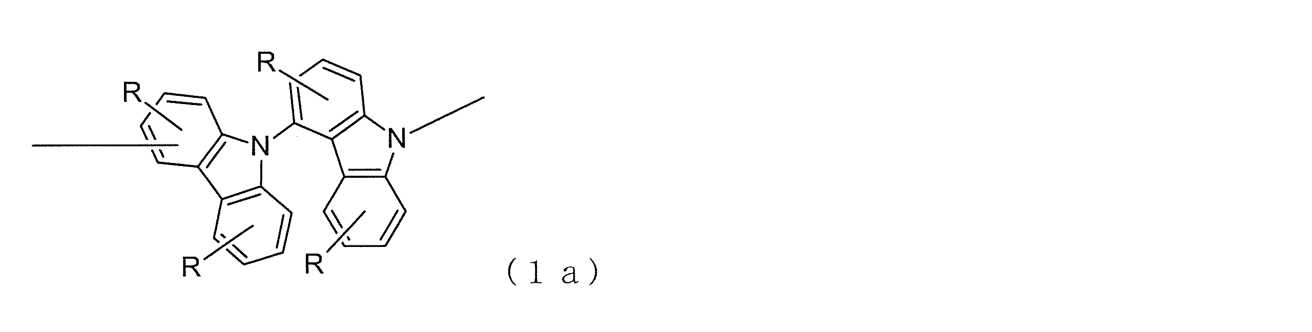
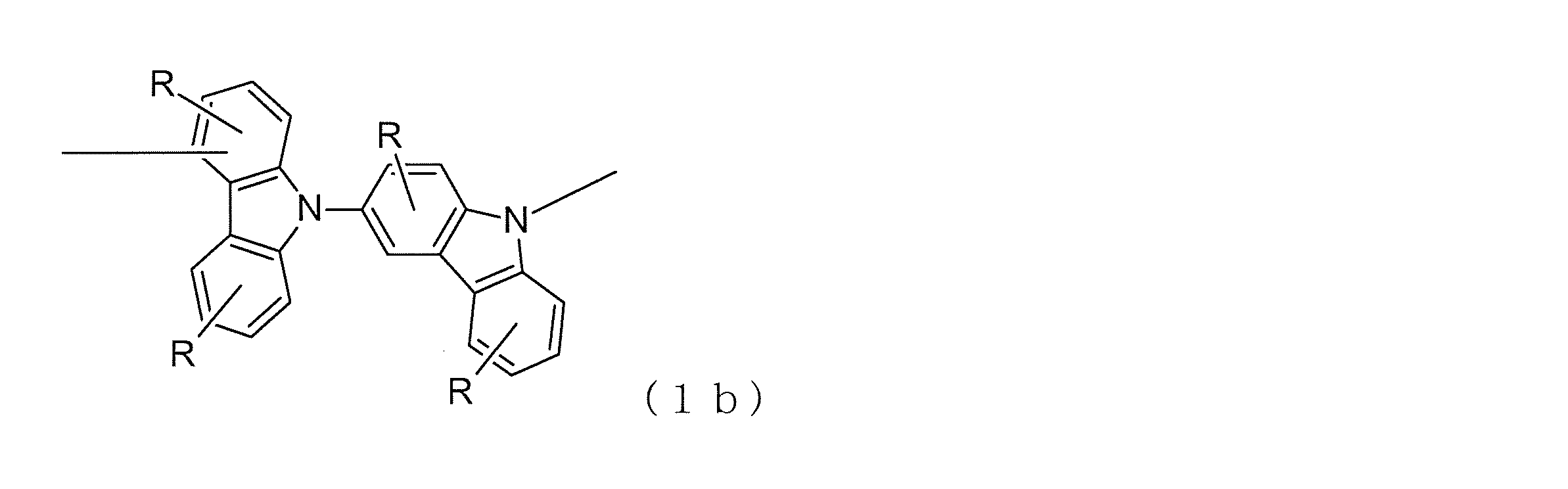
- N is an integer of 1 to 3, and each n is independently an integer of 1 to 4, but at least one n is an integer of 2 to 4, and is represented by at least one formula (1a) in the formula (In general formulas (1) and (1a), each R is independently hydrogen, an alkyl group having 1 to 10 carbon atoms, or a cycloalkyl group having 3 to 11 carbon atoms.)
- n is independently an integer of 1 to 3
- at least one n is preferably an integer of 2 to 3.
- L is preferably an m-valent group generated by removing m hydrogen atoms from any one of the formulas (2) to (5).
- each X independently represents CH or nitrogen
- each R independently represents hydrogen, an alkyl group having 1 to 10 carbon atoms, or a cycloalkyl group having 3 to 11 carbon atoms.
- Y represents oxygen or sulfur
- p represents an integer of 0 to 2.
- L is an m-valent group generated by removing m hydrogen atoms from any one of the formulas (2), (3), or (4).
- the total sum of n is preferably an integer of 2 to 6.
- the present invention relates to the organic electroluminescent element, wherein the organic layer containing a carbazole compound is a light emitting layer containing a phosphorescent dopant.
- the organic electroluminescent device of the present invention contains the carbazole compound represented by the general formula (1) (hereinafter also referred to as the compound represented by the general formula (1)) in the organic layer.
- This carbazole compound has a 4- (9-carbazolyl) carbazole structure, and is considered to bring about the excellent effects as described above.
- L represents an m-valent group formed by removing m hydrogen atoms from an aromatic hydrocarbon having 6 to 30 carbon atoms or an aromatic heterocyclic compound having 3 to 30 carbon atoms.
- L is preferably an m-valent group formed by removing m hydrogen atoms from an aromatic hydrocarbon or aromatic heterocyclic compound having 6 to 18 carbon atoms in total.
- L is not a carbazole ring-containing group.
- the carbazole ring-containing group here is an m-valent group generated by removing m hydrogen atoms from a substituted or unsubstituted carbazole. Specifically, it is an m-valent group generated by removing m hydrogen atoms from N or C constituting the carbazole ring.
- aromatic hydrocarbon or aromatic heterocyclic compound examples include benzene, pentalene, indene, naphthalene, azulene, heptalene, octalene, indacene, acenaphthylene, phenalene, phenanthrene, anthracene, tridene, fluoranthene, acephenanthrylene, and ASEAN.
- Tolylene Triphenylene, Pyrene, Chrysene, Tetraphen, Tetracene, Preaden, Picene, Perylene, Pentaphene, Pentacene, Tetraphenylene, Collanthrylene, Helicene, Hexaphene, Rubicene, Coronene, Trinaphthylene, Heptaphene, Pyrantrene, Furan, Benzofuran, Isobenzofuran , Xanthene, oxatolene, dibenzofuran, perixanthenoxanthene, thiophene, thioxanthene, thianthrene, phen Noxatiin, thionaphthene, isothianaphthene, thiobutene, thiophanthrene, dibenzothiophene, pyrrole, pyrazole, tellurazole, selenazole, thiazole, isothiazole, ox
- the number to be connected is preferably 2 to 10, more preferably 2 to 7, and the connected aromatic rings may be the same or different. Also good.
- the bonding position for bonding to m carbazolyl groups is not limited, and it may be a ring at a terminal portion or a central ring of a linked aromatic ring.
- the aromatic ring is a generic term for an aromatic hydrocarbon ring and an aromatic heterocyclic ring.
- the linked aromatic rings include at least one heterocyclic ring, it is included in the aromatic heterocyclic ring.
- the m-valent group generated from the aromatic compound in which a plurality of aromatic rings are connected is a monovalent group, it is represented by the following formula, for example.
- Ar 1 to Ar 6 represent a substituted or unsubstituted aromatic ring.
- Specific examples of the group formed by connecting a plurality of the aromatic rings include, for example, biphenyl, terphenyl, bipyridine, bipyrimidine, bitriazine, terpyridine, bistriazylbenzene, phenylterphenyl, binaphthalene, phenylpyridine, diphenylpyridine, phenylpyrimidine, diphenyl. And monovalent groups generated by removing hydrogen from pyrimidine, phenyltriazine, diphenyltriazine, phenylnaphthalene, diphenylnaphthalene and the like.
- preferable L forms include m-valent groups generated from the aromatic compounds represented by the formulas (2) to (5), preferably the formulas (2) to (4). These m-valent groups are valent groups generated by removing m hydrogen atoms from the carbon forming the ring appearing in the formulas (2) to (5). When m is 2 or more, the hydrogen atoms to be removed are The same ring may be different.
- each X independently represents methine or nitrogen. Of the Xs constituting each 6-membered ring, 0 to 3 Xs are preferably nitrogen, and more preferably all are methine.
- Y represents oxygen or sulfur.
- p represents an integer of 0 to 2, preferably 0 or 1.
- aromatic compound giving preferable L examples include benzene, pyridine, pyrazine, pyrimidine, pyridazine, triazine, dibenzofuran, dibenzothiophene, biphenyl, terphenyl, bipyridine, bipyrimidine, vitriazine, terpyridine, bistrine.
- Examples include azylbenzene, phenylpyridine, diphenylpyridine, phenylpyrimidine, diphenylpyrimidine, phenyltriazine, diphenyltriazine, phenyldibenzofuran, phenyldibenzothiophene, dibenzofuranylpyridine, and dibenzothienylpyridine. More preferably, benzene, dibenzofuran, dibenzothiophene, biphenyl, terphenyl, bistriazylbenzene, phenyldibenzofuran, and phenyldibenzothiophene are mentioned.
- m represents an integer of 1 to 3.
- m is 1 or 2, more preferably m is 1.
- each n independently represents an integer of 1 to 4.
- n is 1 to 3.
- at least one n is an integer of 2 to 4, and has a bond structure represented by at least one formula (1a) in the formula.
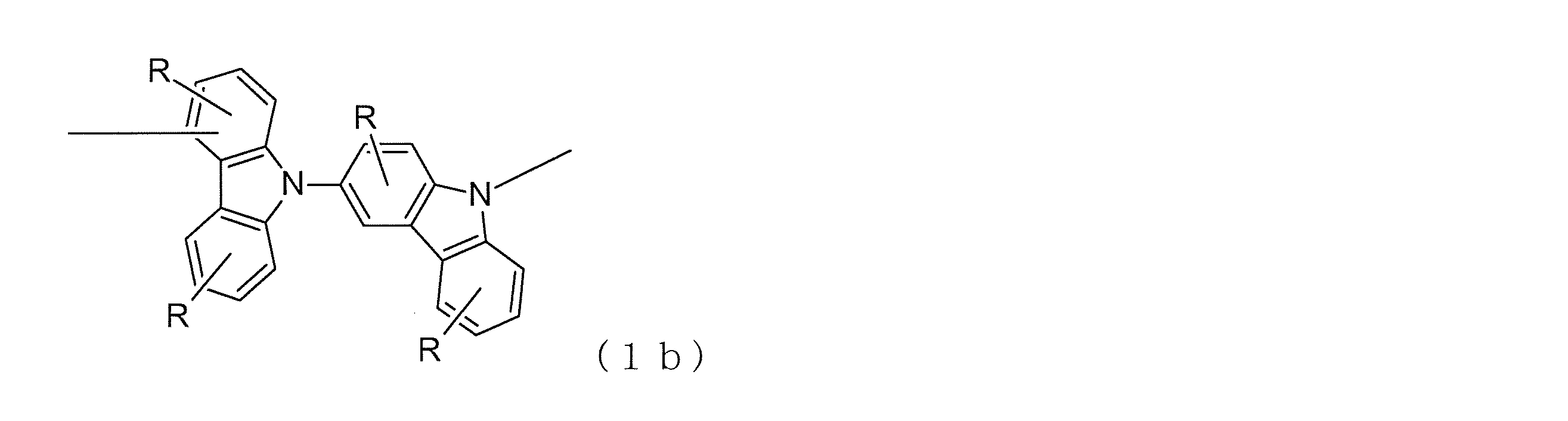
- all the bond structures between carbazole rings are the bond structures represented by the formula (1a) or the formulas (1a) and (1b).
- the carbazole ring refers to a three condensed ring appearing in the general formula (1).
- the total sum of n is an integer of 2 to 12, preferably 2 to 9, and more preferably 2 to 6.
- each R is independently hydrogen, an alkyl group having 1 to 10 carbon atoms, or cycloalkyl having 3 to 11 carbon atoms. Represents a group. Preferred is hydrogen, an alkyl group having 1 to 8 carbon atoms, or a cycloalkyl group having 3 to 8 carbon atoms, and more preferred is hydrogen, an alkyl group having 1 to 4 carbon atoms, or a cycloalkyl group having 5 to 7 carbon atoms. .
- alkyl group examples include a methyl group, an ethyl group, a propyl group, a butyl group, a pentyl group, a hexyl group, a heptyl group, an octyl group, a nonyl group, and a decyl group, preferably a methyl group, an ethyl group, and a propyl group.
- a decyl group preferably a methyl group, an ethyl group, and a propyl group.
- the alkyl group may be linear or branched.
- cycloalkyl group examples include a cyclopropyl group, a cyclobutyl group, a cyclopentyl group, a cyclohexyl group, a cycloheptyl group, a cyclooctyl group, and a methylcyclohexyl group, preferably a cyclohexyl group and a methylcyclohexyl group.
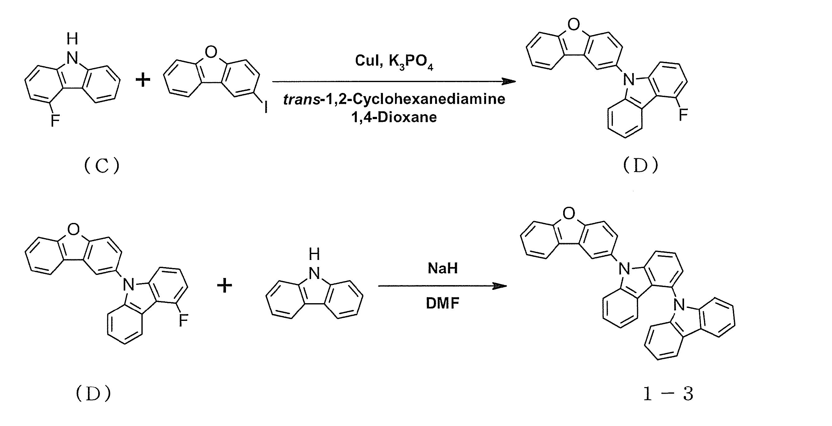
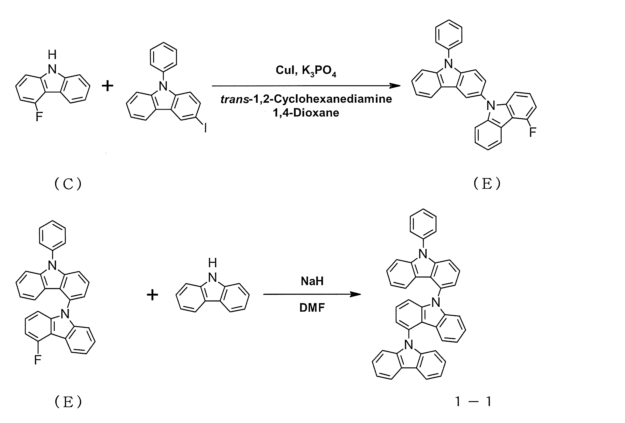
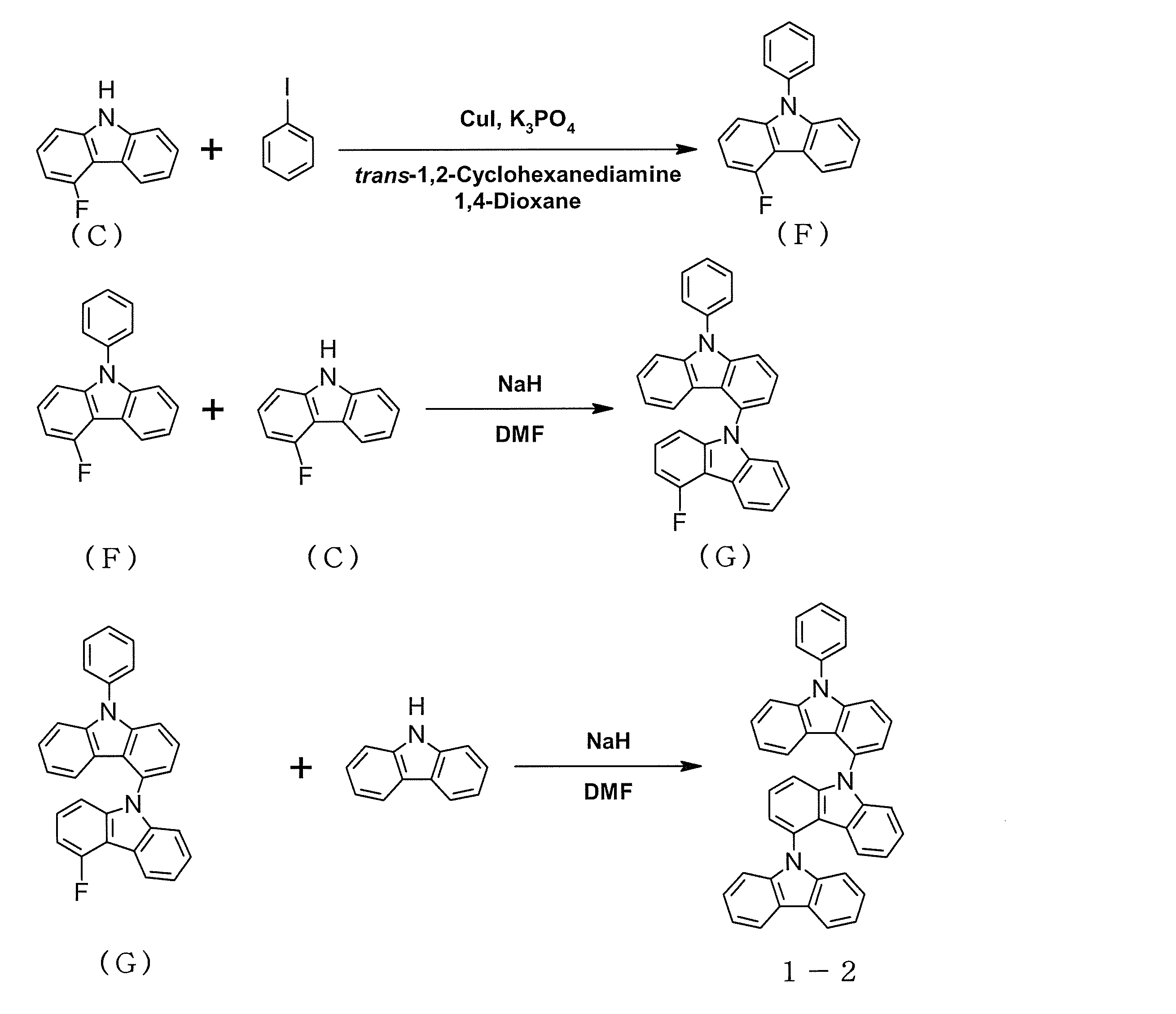
- the carbazole compound of the present invention can be synthesized using a carbazole derivative substituted at the 4-position with a halogen atom, using a known method by selecting a raw material according to the structure of the target compound.
- the 4-fluorocarbazole skeleton of a carbazole derivative substituted at the 4-position with a fluorine atom is described in Journal of Organic Chemistry, 2008, No. 73, p7603 to p7610, and can be synthesized by the following reaction formula with reference to the synthesis examples.
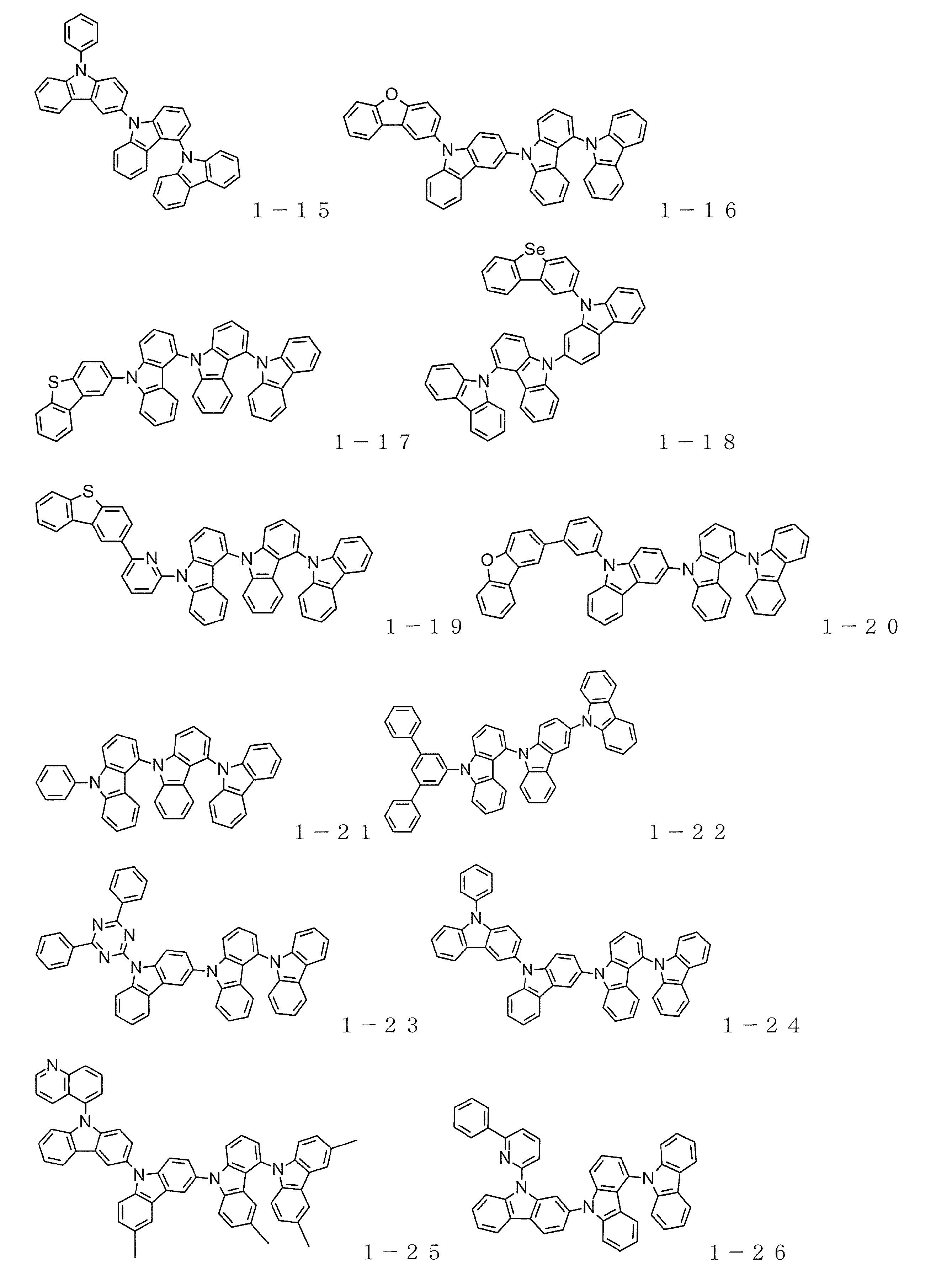
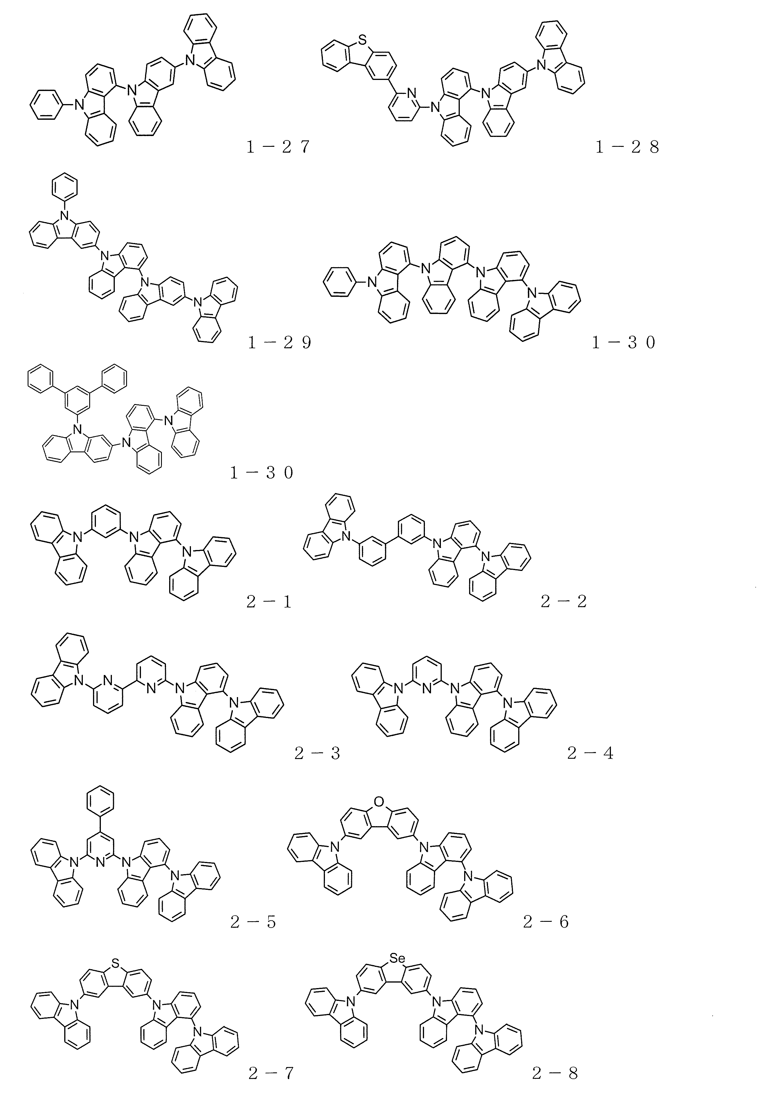
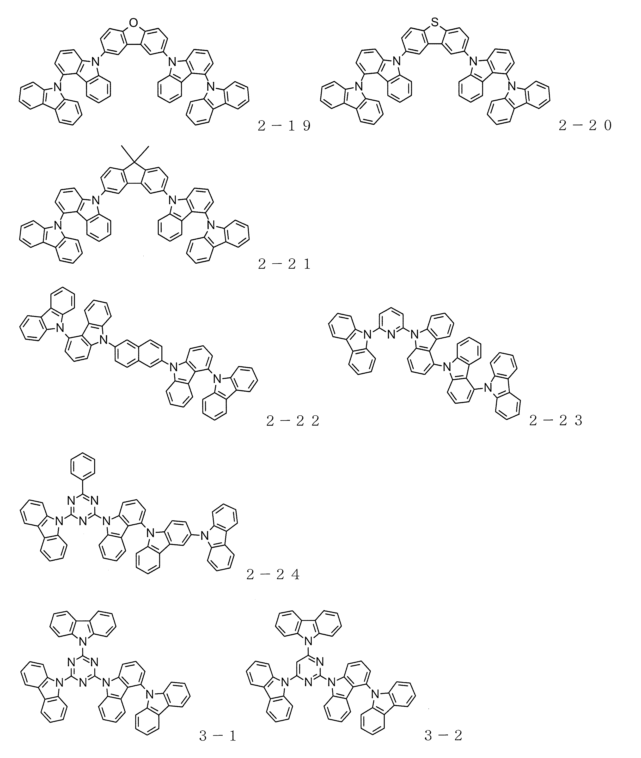
- carbazole compound represented by the general formula (1) Specific examples of the carbazole compound represented by the general formula (1) are shown below, but the material used for the organic electroluminescence device of the present invention is not limited thereto.
- the carbazole compound represented by the general formula (1) includes at least one of a light emitting layer, a hole transport layer, and an electron blocking layer in an organic EL device in which an anode, a plurality of organic layers, and a cathode are stacked on a substrate. By containing it in the organic layer, an excellent organic electroluminescent element is provided.
- a light emitting layer and a positive hole transport layer are preferable. More preferably, it may be contained as a host material of a light emitting layer containing a phosphorescent dopant.
- the organic EL device of the present invention has an organic layer having at least one light emitting layer between an anode and a cathode laminated on a substrate, and at least one of a light emitting layer, a hole transport layer and an electron blocking layer.
- the organic layer contains a compound represented by the general formula (1).
- the light-emitting layer or the hole transport layer contains a compound represented by the general formula (1), and more preferably a compound represented by the general formula (1) together with a phosphorescent dopant is contained in the light-emitting layer. .
- the structure of the organic EL element of the present invention will be described with reference to the drawings.
- the structure of the organic EL element of the present invention is not limited to the illustrated one.
- FIG. 1 is a cross-sectional view showing a structural example of a general organic EL device used in the present invention, wherein 1 is a substrate, 2 is an anode, 3 is a hole injection layer, 4 is a hole transport layer, and 5 is a light emitting layer. , 6 represents an electron transport layer, and 7 represents a cathode.
- the organic EL device of the present invention may have an exciton blocking layer adjacent to the light emitting layer, and may have an electron blocking layer between the light emitting layer and the hole injection layer.
- the exciton blocking layer can be inserted on either the anode side or the cathode side of the light emitting layer, or both can be inserted simultaneously.
- the organic EL device of the present invention has a substrate, an anode, a light emitting layer and a cathode as essential layers, but it is preferable to have a hole injecting and transporting layer and an electron injecting and transporting layer in layers other than the essential layers, and further emit light. It is preferable to have a hole blocking layer between the layer and the electron injecting and transporting layer.
- the hole injection / transport layer means either or both of a hole injection layer and a hole transport layer
- the electron injection / transport layer means either or both of an electron injection layer and an electron transport layer.
- the organic EL element of the present invention is preferably supported on a substrate.
- the substrate is not particularly limited as long as it is conventionally used for an organic EL element.
- a substrate made of glass, transparent plastic, quartz, or the like can be used.
- an electrode material made of a metal, an alloy, an electrically conductive compound, or a mixture thereof having a high work function (4 eV or more) is preferably used.
- electrode materials include metals such as Au, and conductive transparent materials such as CuI, indium tin oxide (ITO), SnO 2 and ZnO.
- conductive transparent materials such as CuI, indium tin oxide (ITO), SnO 2 and ZnO.
- an amorphous material such as IDIXO (In 2 O 3 —ZnO) that can form a transparent conductive film may be used.
- these electrode materials may be formed into a thin film by a method such as vapor deposition or sputtering, and a pattern having a desired shape may be formed by a photolithography method, or when the pattern accuracy is not so high (about 100 ⁇ m or more) ), A pattern may be formed through a mask having a desired shape when the electrode material is deposited or sputtered. Or when using the substance which can be apply
- the transmittance is greater than 10%, and the sheet resistance as the anode is preferably several hundred ⁇ / ⁇ or less.
- the film thickness depends on the material, it is usually selected in the range of 10 to 1000 nm, preferably 10 to 200 nm.
- the cathode a material having a low work function (4 eV or less) metal (referred to as an electron injecting metal), an alloy, an electrically conductive compound, and a mixture thereof as an electrode material is used.
- an electron injecting metal a material having a low work function (4 eV or less) metal
- an alloy a material having a low work function (4 eV or less) metal
- an alloy a material having a low work function (4 eV or less) metal
- an alloy referred to as an electron injecting metal
- an alloy referred to as an electron injecting metal
- a mixture of an electron injecting metal and a second metal which is a stable metal having a larger work function than this for example, a magnesium / silver mixture
- Suitable are a magnesium / aluminum mixture, a magnesium / indium mixture, an aluminum / aluminum oxide (Al 2 O 3 ) mixture, a lithium / aluminum mixture, aluminum and the like.
- the cathode can be produced by forming a thin film of these electrode materials by a method such as vapor deposition or sputtering.
- the sheet resistance as the cathode is preferably several hundred ⁇ / ⁇ or less, and the film thickness is usually selected in the range of 10 nm to 5 ⁇ m, preferably 50 to 200 nm.
- the light emission luminance is improved, which is convenient.
- a transparent or semi-transparent cathode can be produced by producing the conductive transparent material mentioned in the description of the anode on the cathode after producing the metal with a thickness of 1 to 20 nm on the cathode.
- an element in which both the anode and the cathode are transmissive can be manufactured.
- the light emitting layer is a phosphorescent light emitting layer and includes a phosphorescent dopant and a host material.
- the phosphorescent dopant material preferably contains an organometallic complex containing at least one metal selected from ruthenium, rhodium, palladium, silver, rhenium, osmium, iridium, platinum and gold. Such organometallic complexes are known in the prior art documents and the like, and these can be selected and used.
- the emission wavelength of the phosphorescent dopant preferably has a maximum emission wavelength of 550 nm or less.
- Preferred phosphorescent dopants include complexes such as Ir (ppy) 3 having a noble metal element such as Ir as a central metal, complexes such as (Bt) 2 Iracac, and complexes such as (Btp) Ptacac. Specific examples of these complexes are shown below, but are not limited to the following compounds.
- the amount of phosphorescent dopant contained in the light emitting layer is preferably in the range of 1 to 50% by weight. More preferably, it is 5 to 30% by weight.
- the host material in the emissive layer it is preferable to use the compound represented by the general formula (1).
- the material used for the light emitting layer may be a host material other than the compound represented by the general formula (1). .
- a plurality of known host materials may be used in combination.
- a known host compound that can be used is preferably a compound that has a hole transporting ability or an electron transporting ability, prevents the emission of light from becoming longer, and has a high glass transition temperature.
- host materials are known from a large number of patent documents and can be selected from them.
- Specific examples of the host material are not particularly limited, but include indole derivatives, carbazole derivatives, triazole derivatives, oxazole derivatives, oxadiazole derivatives, imidazole derivatives, polyarylalkane derivatives, pyrazoline derivatives, pyrazolone derivatives, phenylenediamine.
- arylamine derivatives amino-substituted chalcone derivatives, styrylanthracene derivatives, fluorenone derivatives, hydrazone derivatives, stilbene derivatives, silazane derivatives, aromatic tertiary amine compounds, styrylamine compounds, aromatic dimethylidene compounds, porphyrin compounds, anthraquino Heterocyclic tetracarboxylic acid anhydrides such as dimethane derivatives, anthrone derivatives, diphenylquinone derivatives, thiopyran dioxide derivatives, naphthalene perylene,
- the injection layer is a layer provided between the electrode and the organic layer for lowering the driving voltage and improving the luminance of light emission.
- the injection layer can be provided as necessary.
- the hole blocking layer has a function of an electron transport layer in a broad sense, and is made of a hole blocking material that has a function of transporting electrons and has a remarkably small ability to transport holes. The probability of recombination of electrons and holes can be improved by blocking.
- a known hole blocking layer material can be used for the hole blocking layer. Moreover, as a hole-blocking layer material, the material of the electron carrying layer mentioned later can be used as needed.
- the electron blocking layer is made of a material that has a function of transporting holes and has a very small ability to transport electrons.
- the electron blocking layer blocks the electrons while transporting holes, and the probability of recombination of electrons and holes. Can be improved.
- the compound represented by the general formula (1) is preferably used. However, when the compound is used for any other organic layer, the material for the hole transport layer described later is used. Can be used as needed.
- the thickness of the electron blocking layer is preferably 3 to 100 nm, more preferably 5 to 30 nm.
- the exciton blocking layer is a layer for preventing excitons generated by recombination of holes and electrons in the light emitting layer from diffusing into the charge transport layer. It becomes possible to efficiently confine in the light emitting layer, and the light emission efficiency of the device can be improved.
- the exciton blocking layer can be inserted on either the anode side or the cathode side adjacent to the light emitting layer, or both can be inserted simultaneously.
- Examples of the material for the exciton blocking layer include 1,3-dicarbazolylbenzene (mCP) and bis (2-methyl-8-quinolinolato) -4-phenylphenolato aluminum (III) (BAlq). It is done.
- mCP 1,3-dicarbazolylbenzene
- BAlq bis (2-methyl-8-quinolinolato) -4-phenylphenolato aluminum
- the hole transport layer is made of a hole transport material having a function of transporting holes, and the hole transport layer can be provided as a single layer or a plurality of layers.
- the hole transport material has either hole injection or transport or electron barrier properties, and may be either organic or inorganic.
- As the hole transport material it is preferable to use the compound represented by the general formula (1). However, when the compound is used in any other organic layer, any one of conventionally known compounds can be used. A thing can be selected and used.
- Examples of known hole transport materials that can be used include triazole derivatives, oxadiazole derivatives, imidazole derivatives, polyarylalkane derivatives, pyrazoline derivatives and pyrazolone derivatives, phenylenediamine derivatives, arylamine derivatives, amino-substituted chalcone derivatives, oxazole derivatives, Examples include styryl anthracene derivatives, fluorenone derivatives, hydrazone derivatives, stilbene derivatives, silazane derivatives, aniline copolymers, and conductive polymer oligomers, particularly thiophene oligomers. Porphyrin compounds, aromatic tertiary amine compounds, and styryl. It is preferable to use an amine compound, and it is more preferable to use an aromatic tertiary amine compound.
- the electron transport layer is made of a material having a function of transporting electrons, and the electron transport layer can be provided as a single layer or a plurality of layers.
- an electron transport material which may also serve as a hole blocking material
- any conventionally known compounds can be selected and used.
- nitro-substituted fluorene derivatives, diphenylquinone derivatives, thiopyran dioxide derivatives, carbodiimides, fluorenylidenemethane derivatives, anthra examples include quinodimethane and anthrone derivatives, oxadiazole derivatives, and the like.
- a thiadiazole derivative in which the oxygen atom of the oxadiazole ring is substituted with a sulfur atom, and a quinoxaline derivative having a quinoxaline ring known as an electron withdrawing group can also be used as an electron transport material.
- a polymer material in which these materials are introduced into a polymer chain or these materials are used as a polymer main chain can also be used.
- intermediate C is 6.4 g (0.034 mol)
- 2-iododibenzofuran is 21.5 g (0.073 mol)
- copper iodide is 36.2 g (0.19 mol)
- trans- 1,2-cyclohexanediamine (23.1 ml, 0.19 mol)
- 1,4-dioxane (162 ml) were added, and the mixture was stirred at 120 ° C overnight.
- the precipitated crystals were collected by filtration, and the solvent was distilled off under reduced pressure.
- the obtained residue was purified by silica gel column chromatography to obtain 7.0 g (0.020 mol, yield 58%) of intermediate D as a white solid.
- Example 1 In the organic EL device shown in FIG. 1, a device in which an electron injection layer was added between the electron transport layer and the cathode was produced. Each thin film was laminated at a vacuum degree of 2.0 ⁇ 10 ⁇ 5 Pa by a vacuum deposition method on a glass substrate on which an anode made of indium tin oxide (ITO) having a thickness of 110 nm was formed. First, copper phthalocyanine (CuPC) was formed to a thickness of 25 nm on ITO as a hole injection layer. Next, N, N-di (naphthalen-1-yl) -N, N-diphenyl-benzidene (NPB) was formed to a thickness of 90 nm as a hole transport layer.
- ITO indium tin oxide
- compound 1-3 as a host material of the light emitting layer and an iridium complex [iridium (III) bis (4,6-di-fluorophenyl) -pyridinate as a blue phosphorescent material as a dopant -N, C2 ′] picolinate] (FIrpic) were co-deposited from different deposition sources to form a light emitting layer with a thickness of 30 nm. The concentration of FIrpic was 10%.
- Alq3 was formed to a thickness of 30 nm as an electron transport layer.
- lithium fluoride (LiF) was formed to a thickness of 1.0 nm as an electron injection layer.
- Al aluminum
- Al was formed as an electrode to a thickness of 70 nm on the electron injection layer, and an organic EL element was produced.
- Examples 2 to 11 As a host material of the light emitting layer, compound 1-8, compound 1-11, compound 1-15, compound 1-17, compound 1-21, compound 1-27, compound 1-30, compound 2-13, compound 2- An organic EL device was produced in the same manner as in Example 1 except that 23 or Compound 3-6 was used.
- Comparative Examples 1 and 2 An organic EL device was produced in the same manner as in Example 1 except that mCP or the following compound H-1 was used as the host material of the light emitting layer.
- the organic EL elements When an external power source was connected to the organic EL elements obtained in the above Examples and Comparative Examples and a direct current voltage was applied, it was confirmed that the organic EL elements had light emission characteristics (initial characteristics) as shown in Table 1.
- the maximum wavelength of the device emission spectrum was 475 nm, indicating that light emission from FIrpic was obtained.
- the compound is a compound used as a host material, and luminance, voltage, and luminous efficiency show values at 2.5 mA / cm 2 .
- Example 12 Each thin film was laminated at a vacuum degree of 2.0 ⁇ 10 ⁇ 5 Pa by a vacuum deposition method on a glass substrate on which an anode made of an ITO substrate having a thickness of 110 nm was formed.
- CuPC was formed to a thickness of 25 nm on ITO as a hole injection layer.
- NPB was formed to a thickness of 40 nm as a hole transport layer.
- Compound 1-3 as a host material and Ir (ppy) 3 as a dopant were co-deposited from different vapor deposition sources on the hole transport layer to form a light emitting layer having a thickness of 40 nm. At this time, the concentration of Ir (ppy) 3 was 10 wt%.
- Alq3 was formed to a thickness of 20 nm as an electron transport layer. Further, LiF was formed to a thickness of 1 nm as an electron injection layer on the electron transport layer. Finally, on the electron injection layer, Al was formed to a thickness of 70 nm as an electrode to produce an organic EL device.
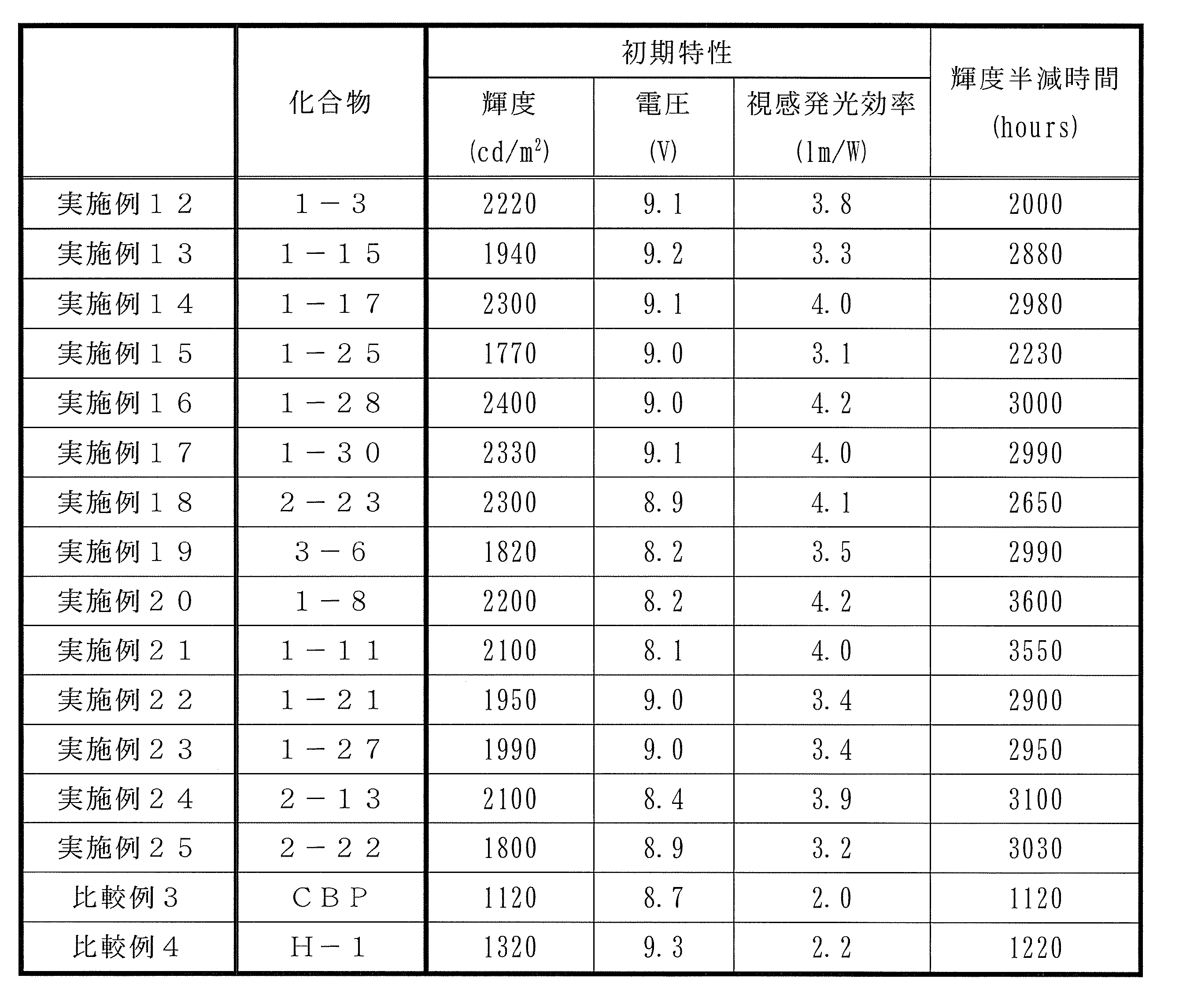
- Examples 13-25 As a host material of the light emitting layer, compound 1-8, compound 1-11, compound 1-15, compound 1-17, compound 1-21, compound 1-25, compound 1-27, compound 1-28, compound 1- 30, an organic EL device was produced in the same manner as in Example 12 except that Compound 2-13, Compound 2-22, Compound 2-23, or Compound 3-6 was used.
- Comparative Examples 3-4 An organic EL device was produced in the same manner as in Example 12 except that CBP or H-1 was used as the host material of the light emitting layer.
- Examples 12 to 25 using the compound represented by the general formula (1) in the light-emitting layer are different in CBP generally known as a phosphorescent host material and H-1 having different carbazole substitution positions. It can be seen that it has higher luminous efficiency characteristics than the case of using. It also shows that the drive life characteristics are good and the stability is high.
- the carbazole compound represented by the general formula (1) has a 4- (9-carbazolyl) carbazole structure, so that it is possible to control the spread of molecular orbitals, to optimize charge balance and to stabilize both charges. Is considered to have an improved effect. Further, it is clear that a highly efficient organic EL phosphor element is realized by using the compound for the light emitting layer.
- the carbazole compound used in the present invention has a 4- (9-carbazolyl) carbazole structure.
- a compound having only a 3- (9-carbazolyl) carbazole structure as shown in Patent Document 5 is known. Since the compound of the present invention has a 4- (9-carbazolyl) carbazole structure, the compound of the present invention exhibits higher hole transportability than the case where carbazole is linked only at other positions. Further, it is considered that the electron transporting property can be improved while ensuring high hole transporting property by substituting the linking group with a specific aromatic group.
- the carbazole compound used in the present invention when used as a host material, it is considered that the transport property of both charges is increased and the recombination probability in the light emitting layer is increased. Due to the above effects, it is considered that the organic EL element of the present invention can achieve a high light emission efficiency, a long driving life, and a highly durable organic EL element.
- the organic EL device according to the present invention has practically satisfactory levels in terms of light emission characteristics, driving life and durability, flat panel display (mobile phone display device, in-vehicle display device, OA computer display device, television, etc.), surface light emission, etc. Its technical value is great in applications to light sources (lighting, light sources for copying machines, backlight light sources for liquid crystal displays and instruments), display boards, and sign lamps that make use of the characteristics of the body.
Abstract
Description


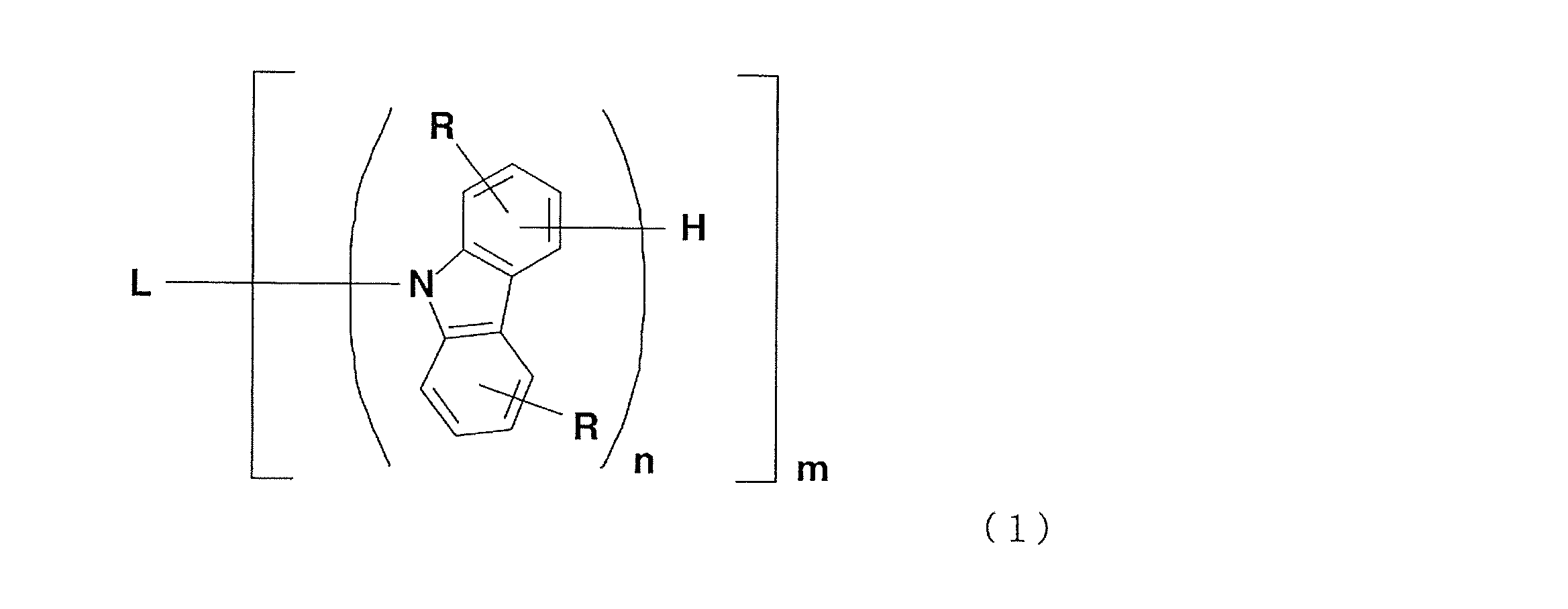
(ここで、Lはm価の総炭素数6~30の芳香族炭化水素基又は総炭素数3~30の芳香族複素環基であるが、カルバゾール環含有基であることはない。mは1~3の整数であり、nはそれぞれ独立して1~4の整数であるが、少なくとも1つのnは2~4の整数であり、式中に少なくとも1つの式(1a)で表される結合構造を有する。一般式(1)及び式(1a)中、Rはそれぞれ独立して水素、炭素数1~10のアルキル基又は炭素数3~11のシクロアルキル基である。)
(ここで、Rは式(1a)と同意である。)

(式(2)~(5)中、Xはそれぞれ独立してCH又は窒素を表し、Rはそれぞれ独立して水素、炭素数1~10のアルキル基又は炭素数3~11のシクロアルキル基を表す。式(3)及び(5)中、Yは酸素又は硫黄を表し、式(4)中、pは0~2の整数を表す。)
また、一般式(1)において、nの総和が2~6の整数であることが好ましい。
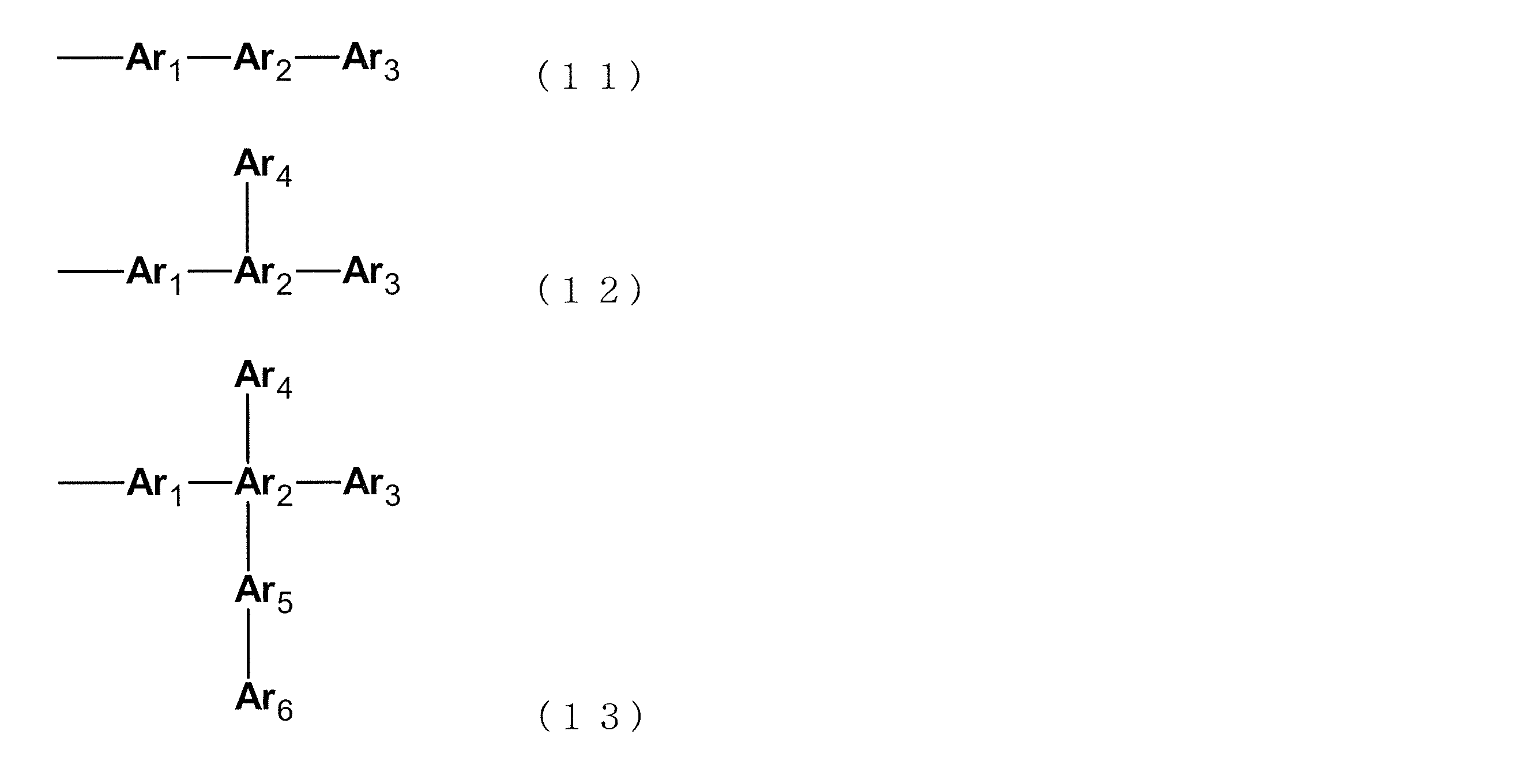
(式(11)~(13)中、Ar1~Ar6は、置換又は無置換の芳香環を示す。)


本発明の有機EL素子は、基板に支持されていることが好ましい。この基板については、特に制限はなく、従来から有機EL素子に慣用されているものであればよく、例えば、ガラス、透明プラスチック、石英などからなるものを用いることができる。
有機EL素子における陽極としては、仕事関数の大きい(4eV以上)金属、合金、電気伝導性化合物及びこれらの混合物を電極物質とするものが好ましく用いられる。このような電極物質の具体例としてはAu等の金属、CuI、インジウムチンオキシド(ITO)、SnO2、ZnO等の導電性透明材料が挙げられる。また、IDIXO(In2O3-ZnO)等非晶質で透明導電膜を作製可能な材料を用いてもよい。陽極はこれらの電極物質を蒸着やスパッタリング等の方法により、薄膜を形成させ、フォトリソグラフィー法で所望の形状のパターンを形成してもよく、あるいはパターン精度をあまり必要としない場合は(100μm以上程度)、上記電極物質の蒸着やスパッタリング時に所望の形状のマスクを介してパターンを形成してもよい。あるいは、有機導電性化合物のように塗布可能な物質を用いる場合には、印刷方式、コーティング方式等湿式成膜法を用いることもできる。この陽極より発光を取り出す場合には、透過率を10%より大きくすることが望ましく、また陽極としてのシート抵抗は数百Ω/□以下が好ましい。更に膜厚は材料にもよるが、通常10~1000nm、好ましくは10~200nmの範囲で選ばれる。
一方、陰極としては、仕事関数の小さい(4eV以下)金属(電子注入性金属と称する)、合金、電気伝導性化合物及びこれらの混合物を電極物質とするものが用いられる。このような電極物質の具体例としては、ナトリウム、ナトリウム-カリウム合金、マグネシウム、リチウム、マグネシウム/銅混合物、マグネシウム/銀混合物、マグネシウム/アルミニウム混合物、マグネシウム/インジウム混合物、アルミニウム/酸化アルミニウム(Al2O3)混合物、インジウム、リチウム/アルミニウム混合物、希土類金属等が挙げられる。これらの中で、電子注入性及び酸化等に対する耐久性の点から、電子注入性金属とこれより仕事関数の値が大きく安定な金属である第二金属との混合物、例えば、マグネシウム/銀混合物、マグネシウム/アルミニウム混合物、マグネシウム/インジウム混合物、アルミニウム/酸化アルミニウム(Al2O3)混合物、リチウム/アルミニウム混合物、アルミニウム等が好適である。陰極はこれらの電極物質を蒸着やスパッタリング等の方法により薄膜を形成させることにより、作製することができる。また、陰極としてのシート抵抗は数百Ω/□以下が好ましく、膜厚は通常10nm~5μm、好ましくは50~200nmの範囲で選ばれる。なお、発光した光を透過させるため、有機EL素子の陽極又は陰極のいずれか一方が、透明又は半透明であれば発光輝度が向上し好都合である。
発光層は燐光発光層であり、燐光発光ドーパントとホスト材料を含む。燐光発光ドーパント材料としては、ルテニウム、ロジウム、パラジウム、銀、レニウム、オスミウム、イリジウム、白金及び金から選ばれる少なくとも1つの金属を含む有機金属錯体を含有するものがよい。かかる有機金属錯体は、前記先行技術文献等で公知であり、これらが選択されて使用可能である。燐光発光ドーパントの発光波長は550nm以下に発光極大波長を有することが望ましい。


注入層とは、駆動電圧低下や発光輝度向上のために電極と有機層間に設けられる層のことで、正孔注入層と電子注入層があり、陽極と発光層又は正孔輸送層の間、及び陰極と発光層又は電子輸送層との間に存在させてもよい。注入層は必要に応じて設けることができる。
正孔阻止層とは広い意味では電子輸送層の機能を有し、電子を輸送する機能を有しつつ正孔を輸送する能力が著しく小さい正孔阻止材料からなり、電子を輸送しつつ正孔を阻止することで電子と正孔の再結合確率を向上させることができる。
電子阻止層とは、正孔を輸送する機能を有しつつ電子を輸送する能力が著しく小さい材料から成り、正孔を輸送しつつ電子を阻止することで電子と正孔が再結合する確率を向上させることができる。
励起子阻止層とは、発光層内で正孔と電子が再結合することにより生じた励起子が電荷輸送層に拡散することを阻止するための層であり、本層の挿入により励起子を効率的に発光層内に閉じ込めることが可能となり、素子の発光効率を向上させることができる。励起子阻止層は発光層に隣接して陽極側、陰極側のいずれにも挿入することができ、両方同時に挿入することも可能である。
正孔輸送層とは正孔を輸送する機能を有する正孔輸送材料からなり、正孔輸送層は単層又は複数層設けることができる。
電子輸送層とは電子を輸送する機能を有する材料からなり、電子輸送層は単層又は複数層設けることができる。
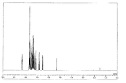
化合物1-3の合成

APCI-TOFMS, m/z 498 [M]+ 、1H-NMR測定結果(測定溶媒:CD2Cl2)を図2に示す。
化合物1-15の合成
化合物1-21の合成
化合物1-27の合成
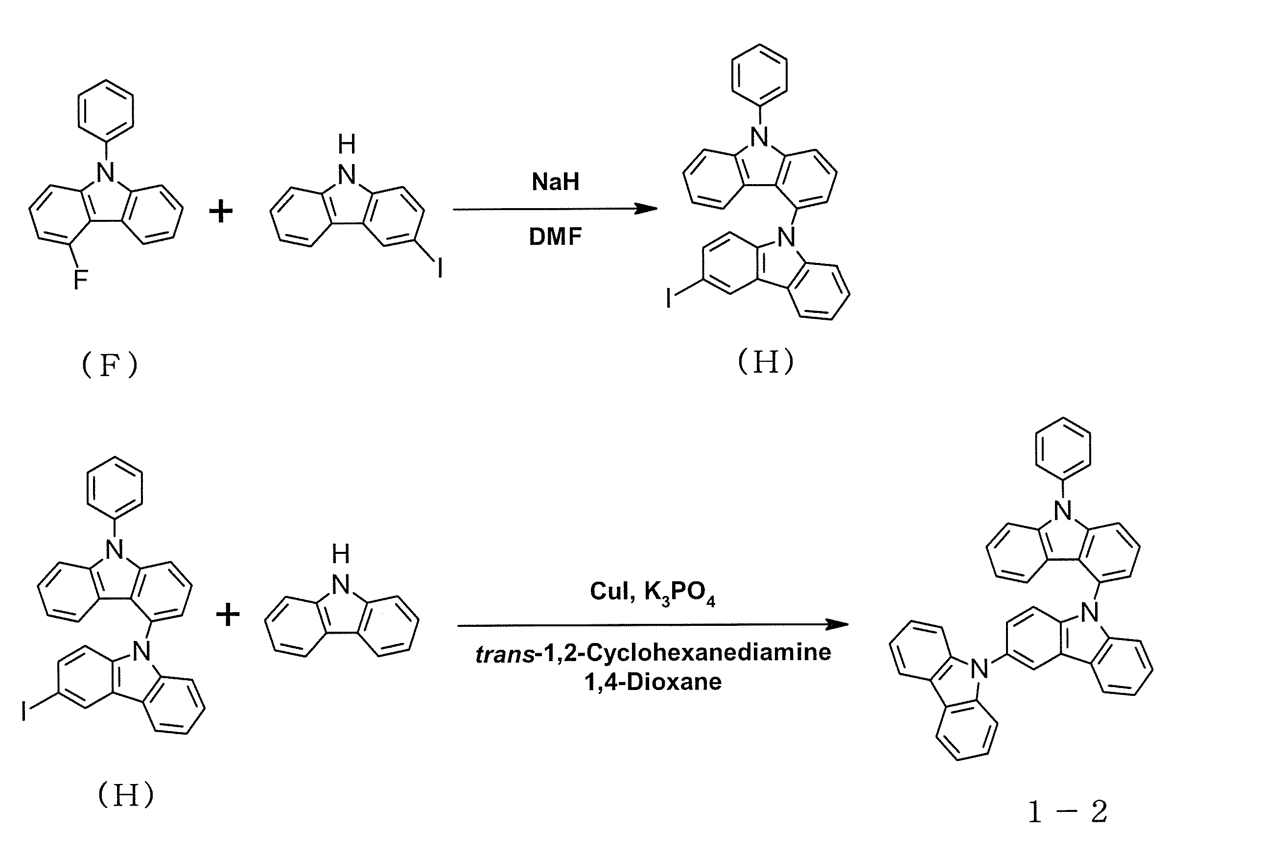
図1に示す有機EL素子において、電子輸送層と陰極との間に電子注入層を追加した素子を作製した。膜厚 110 nm の 酸化インジウムスズ(ITO)からなる陽極が形成されたガラス基板上に、各薄膜を真空蒸着法にて、真空度2.0×10⁻⁵ Pa で積層させた。まず、ITO 上に正孔注入層として、銅フタロシアニン(CuPC)を 25 nm の厚さに形成した。次に、正孔輸送層としてN,N-ジ(ナフタレン-1-イル)-N,N-ジフェニル-ベンジデン(NPB)を 90 nm の厚さに形成した。次に、正孔輸送層上に、発光層のホスト材料としての化合物1-3とドーパントとしての青色燐光材料であるイリジウム錯体[イリジウム(III)ビス(4,6-ジ-フルオロフェニル)-ピリジネート-N,C2']ピコリネート](FIrpic)とを異なる蒸着源から、共蒸着し、30 nm の厚さに発光層を形成した。FIrpicの濃度は 10 %であった。次に、電子輸送層として Alq3 を 30 nm厚さに形成した。更に、電子輸送層上に、電子注入層としてフッ化リチウム(LiF)を 1.0 nm厚さに形成した。最後に、電子注入層上に、電極としてアルミニウム(Al)を70 nm厚さに形成し、有機EL素子を作製した。
発光層のホスト材料として、化合物1-8、化合物1-11、化合物1-15、化合物1-17、化合物1-21、化合物1-27、化合物1-30、化合物2-13、化合物2-23又は化合物3-6を用いた以外は実施例1と同様にして有機EL素子を作製した。
発光層のホスト材料として、mCP又は下記化合物H-1を用いた以外は実施例1と同様にして有機EL素子を作製した。
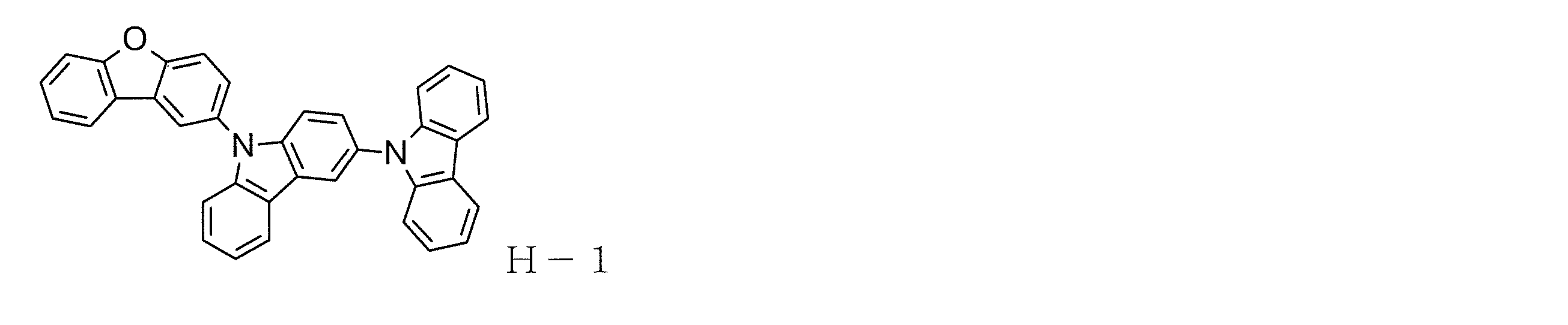
表1において、化合物はホスト材料として使用した化合物であり、輝度、電圧、及び発光効率は、2.5 mA/cm2での値を示す。

膜厚110nmのITO基板からなる陽極が形成されたガラス基板上に、各薄膜を真空蒸着法にて、真空度2.0×10⁻⁵Paで積層させた。まず、ITO上に正孔注入層として、CuPCを 25 nm の厚さに形成した。次に、正孔輸送層としてNPBを40 nmの厚さに形成した。次に、正孔輸送層上に、ホスト材料としての化合物1-3とドーパントとしてのIr(ppy)3とを異なる蒸着源から、共蒸着し、40 nmの厚さに発光層を形成した。この時、Ir(ppy)3の濃度は10 wt%であった。次に、電子輸送層としてAlq3を20nmの厚さに形成した。更に、電子輸送層上に、電子注入層としてLiFを1nmの厚さに形成した。最後に、電子注入層上に、電極としてAlを70nmの厚さに形成し、有機EL素子を作製した。
発光層のホスト材料として、化合物1-8、化合物1-11、化合物1-15、化合物1-17、化合物1-21、化合物1-25、化合物1-27、化合物1-28、化合物1-30、化合物2-13、化合物2-22、化合物2-23又は化合物3-6を用いた以外は実施例12と同様にして有機EL素子を作製した。
発光層のホスト材料としてCBP又はH-1を用いた以外は実施例12と同様にして有機EL素子を作製した。
表2において、化合物はホスト材料として使用した化合物であり、輝度、電圧及び発光効率は、20 mA/cm2での駆動時の値を示し、また、輝度半減時間は、20 mA/cm2の一定電流駆動で評価し、この結果を初期輝度1000 cd/m2の場合に換算した値を示す。
Claims (7)
- 基板上に、陽極、複数の有機層及び陰極が積層されてなる有機電界発光素子において、発光層、正孔輸送層及び電子阻止層からなる群れから選ばれる少なくとも一つの層に一般式(1)で表されるカルバゾール化合物を含有することを特徴とする有機電界発光素子。

ここで、Lはm価の総炭素数6~30の芳香族炭化水素基又は総炭素数3~30の芳香族複素環基であるが、カルバゾール環含有基であることはない。Rはそれぞれ独立して水素、炭素数1~10のアルキル基又は炭素数3~11のシクロアルキル基である。mは1~3の整数であり、nはそれぞれ独立して1~4の整数であるが、少なくとも1つのnは2~4の整数であり、式中に少なくとも1つの式(1a)で表される結合構造を有する。

ここで、Rは一般式(1)と同意である。 - 一般式(1)において、mは1~2の整数であり、nはそれぞれ独立して1~3の整数であり、少なくとも1つのnは2~3の整数である請求項1に記載の有機電界発光素子。
- 一般式(1)において、カルバゾール環間の全ての結合構造が式(1a)、又は式(1a)及び下記式(1b)で表される結合構造である請求項2に記載の有機電界発光素子。
ここで、Rは式(1a)と同意である。 - 一般式(1)において、Lが式(2)~(5)のいずれか1つからm個の水素を除いて生じるm価の基である請求項1に記載の有機電界発光素子。

式(2)~(5)中、Xはそれぞれ独立してCH又は窒素を表し、Rはそれぞれ独立して水素、炭素数1~10のアルキル基又は炭素数3~11のシクロアルキル基を表す。式(3)及び(5)中、Yは酸素又は硫黄を表し、式(4)中、pは0~2の整数を表す。 - 一般式(1)において、Lが式(2)~(4)のいずれか1つからm個の水素を除いて生じるm価の基である請求項4に記載の有機電界発光素子。
- 一般式(1)において、nの総和が2~6の整数である請求項1に記載の有機電界発光素子。
- カルバゾール化合物を含む有機層が、燐光発光ドーパントを含有する発光層であることを特徴とする請求項1~6のいずれかに記載の有機電界発光素子。
Priority Applications (5)
| Application Number | Priority Date | Filing Date | Title |
|---|---|---|---|
| EP11846896.6A EP2650941B1 (en) | 2010-12-09 | 2011-11-28 | Organic electroluminescent element |
| CN201180059022.XA CN103262283B (zh) | 2010-12-09 | 2011-11-28 | 有机电致发光元件 |
| JP2012547786A JP5834023B2 (ja) | 2010-12-09 | 2011-11-28 | 有機電界発光素子 |
| US13/990,511 US9337432B2 (en) | 2010-12-09 | 2011-11-28 | Organic electroluminescent element |
| KR1020137017654A KR101838675B1 (ko) | 2010-12-09 | 2011-11-28 | 유기 전계 발광 소자 |
Applications Claiming Priority (2)
| Application Number | Priority Date | Filing Date | Title |
|---|---|---|---|
| JP2010274334 | 2010-12-09 | ||
| JP2010-274334 | 2010-12-09 |
Publications (1)
| Publication Number | Publication Date |
|---|---|
| WO2012077520A1 true WO2012077520A1 (ja) | 2012-06-14 |
Family
ID=46207012
Family Applications (1)
| Application Number | Title | Priority Date | Filing Date |
|---|---|---|---|
| PCT/JP2011/077384 WO2012077520A1 (ja) | 2010-12-09 | 2011-11-28 | 有機電界発光素子 |
Country Status (7)
| Country | Link |
|---|---|
| US (1) | US9337432B2 (ja) |
| EP (1) | EP2650941B1 (ja) |
| JP (1) | JP5834023B2 (ja) |
| KR (1) | KR101838675B1 (ja) |
| CN (1) | CN103262283B (ja) |
| TW (1) | TWI518071B (ja) |
| WO (1) | WO2012077520A1 (ja) |
Cited By (20)
| Publication number | Priority date | Publication date | Assignee | Title |
|---|---|---|---|---|
| WO2013035275A1 (ja) * | 2011-09-09 | 2013-03-14 | 出光興産株式会社 | 含窒素へテロ芳香族環化合物 |
| WO2013062043A1 (ja) * | 2011-10-26 | 2013-05-02 | 東ソー株式会社 | 4-アミノカルバゾール化合物及びその用途 |
| WO2013081088A1 (ja) * | 2011-12-02 | 2013-06-06 | 国立大学法人九州大学 | 有機発光素子ならびにそれに用いる遅延蛍光材料および化合物 |
| WO2013165192A1 (en) * | 2012-05-02 | 2013-11-07 | Rohm And Haas Electronic Materials Korea Ltd. | Novel organic electroluminescence compounds and organic electroluminescence device containing the same |
| CN103570712A (zh) * | 2012-07-31 | 2014-02-12 | 乐金显示有限公司 | 磷光化合物和使用该磷光化合物的有机发光二极管器件 |
| US20150243894A1 (en) * | 2014-02-21 | 2015-08-27 | Universal Display Corporation | Organic Electroluminescent Materials and Devices |
| KR101550429B1 (ko) * | 2013-04-30 | 2015-09-08 | (주)피엔에이치테크 | 새로운 유기전계발광소자용 화합물 및 그를 포함하는 유기전계발광소자 |
| EP3034506A1 (en) | 2014-12-15 | 2016-06-22 | Idemitsu Kosan Co., Ltd | 4-functionalized carbazole derivatives for electronic applications |
| KR20160092983A (ko) | 2013-12-18 | 2016-08-05 | 이데미쓰 고산 가부시키가이샤 | 화합물, 유기 전기발광 소자용 재료, 잉크 조성물, 유기 전기발광 소자, 전자 기기, 및 화합물의 제조 방법 |
| WO2016158191A1 (ja) * | 2015-03-30 | 2016-10-06 | 新日鉄住金化学株式会社 | 有機電界発光素子 |
| TWI567069B (zh) * | 2012-07-19 | 2017-01-21 | 新日鐵住金化學股份有限公司 | 有機電場發光元件 |
| US9698352B2 (en) | 2012-09-27 | 2017-07-04 | Tosoh Corporation | Amine compound and use thereof |
| WO2017115596A1 (ja) * | 2015-12-28 | 2017-07-06 | 新日鉄住金化学株式会社 | 有機電界発光素子 |
| WO2017169785A1 (ja) * | 2016-03-28 | 2017-10-05 | 新日鉄住金化学株式会社 | 有機電界発光素子 |
| WO2018173598A1 (ja) * | 2017-03-22 | 2018-09-27 | 新日鉄住金化学株式会社 | 有機電界発光素子 |
| WO2018173593A1 (ja) * | 2017-03-23 | 2018-09-27 | 新日鉄住金化学株式会社 | 有機電界発光素子 |
| KR20190025512A (ko) * | 2017-09-01 | 2019-03-11 | 주식회사 엘지화학 | 신규한 화합물 및 이를 이용한 유기발광 소자 |
| JP2019116461A (ja) * | 2017-12-27 | 2019-07-18 | 三星電子株式会社Samsung Electronics Co.,Ltd. | 化合物、有機エレクトロルミネッセンス素子用液状組成物、有機エレクトロルミネッセンス素子用インク組成物、有機エレクトロルミネッセンス素子用薄膜、及び有機エレクトロルミネッセンス素子 |
| WO2022124367A1 (ja) | 2020-12-11 | 2022-06-16 | 日鉄ケミカル&マテリアル株式会社 | 有機電界発光素子用材料及び有機電界発光素子 |
| US11706977B2 (en) | 2018-01-11 | 2023-07-18 | Samsung Electronics Co., Ltd. | Heterocyclic compound, composition including the same, and organic light-emitting device including the heterocyclic compound |
Families Citing this family (9)
| Publication number | Priority date | Publication date | Assignee | Title |
|---|---|---|---|---|
| EP2709181B1 (en) * | 2011-05-12 | 2016-08-10 | Toray Industries, Inc. | Light-emitting element material and light-emitting element |
| US10418564B2 (en) | 2014-04-11 | 2019-09-17 | Merck Patent Gmbh | Materials for organic electroluminescent devices |
| US9312499B1 (en) | 2015-01-05 | 2016-04-12 | Universal Display Corporation | Organic electroluminescent materials and devices |
| US9834808B2 (en) | 2016-01-21 | 2017-12-05 | SeLux Diagnostics, Inc. | Methods for rapid antibiotic susceptibility testing |
| JP7046833B2 (ja) | 2016-01-21 | 2022-04-04 | セルックス・ダイアグノスティクス・インコーポレイテッド | 迅速な抗菌剤感受性試験のための方法 |
| KR102637650B1 (ko) * | 2016-11-30 | 2024-02-15 | 엘지디스플레이 주식회사 | 유기 화합물과 이를 포함하는 유기발광다이오드 및 유기발광 표시장치 |
| WO2018116152A1 (en) * | 2016-12-19 | 2018-06-28 | Idemitsu Kosan Co., Ltd. | Specifically substituted ladder type compounds for organic light emitting devices |
| EP3559252A1 (en) | 2016-12-23 | 2019-10-30 | Selux Diagnostics, Inc. | Methods for improved rapid antimicrobial susceptibility testing |
| CN111548342B (zh) * | 2020-05-12 | 2024-01-19 | 中国科学院长春应用化学研究所 | 以三嗪为中心核的树枝状双极主体材料、制备方法及其在有机电致发光器件上的应用 |
Citations (6)
| Publication number | Priority date | Publication date | Assignee | Title |
|---|---|---|---|---|
| JP2001220380A (ja) * | 2000-02-08 | 2001-08-14 | Samsung Sdi Co Ltd | 高い熱安定性を持つ有機電界発光素子用正孔輸送性化合物及びその製造方法並びに有機電界発光素子 |
| WO2008059943A1 (fr) * | 2006-11-16 | 2008-05-22 | Bando Chemical Industries, Ltd. | Dérivé inédit du carbazole et utilisation de celui-ci |
| WO2009086028A2 (en) * | 2007-12-28 | 2009-07-09 | Universal Display Corporation | Carbazole-containing materials in phosphorescent light emitting diodes |
| WO2011049325A2 (en) * | 2009-10-21 | 2011-04-28 | Cheil Industries Inc. | Novel compound for organic photoelectric device and organic photoelectric device including the same |
| WO2011057706A2 (de) * | 2009-11-14 | 2011-05-19 | Merck Patent Gmbh | Materialien für elektronische vorrichtungen |
| WO2011081061A1 (ja) * | 2009-12-28 | 2011-07-07 | 新日鐵化学株式会社 | 有機電界発光素子 |
Family Cites Families (12)
| Publication number | Priority date | Publication date | Assignee | Title |
|---|---|---|---|---|
| JP4707082B2 (ja) * | 2002-11-26 | 2011-06-22 | コニカミノルタホールディングス株式会社 | 有機エレクトロルミネッセンス素子および表示装置 |
| US7279704B2 (en) * | 2004-05-18 | 2007-10-09 | The University Of Southern California | Complexes with tridentate ligands |
| US7402345B2 (en) | 2004-09-14 | 2008-07-22 | E.I. Du Pont De Nemours And Company | Electroluminescent iridium compounds with fluorinated phenylpyridine ligands, and devices made with such compounds |
| JP2008195841A (ja) * | 2007-02-14 | 2008-08-28 | Toray Ind Inc | 発光素子材料および発光素子 |
| EP2129739B1 (en) * | 2007-03-28 | 2011-06-08 | FUJIFILM Corporation | Organic electroluminescent device |
| US20080284317A1 (en) | 2007-05-17 | 2008-11-20 | Liang-Sheng Liao | Hybrid oled having improved efficiency |
| JP5194596B2 (ja) * | 2007-07-11 | 2013-05-08 | コニカミノルタホールディングス株式会社 | 有機エレクトロルミネッセンス素子、表示装置及び照明装置 |
| US9067947B2 (en) | 2009-01-16 | 2015-06-30 | Universal Display Corporation | Organic electroluminescent materials and devices |
| CN101580521B (zh) * | 2009-04-21 | 2012-09-05 | 中国科学院长春应用化学研究所 | 树枝状有机金属配合物及用该配合物的电致发光器件 |
| JP4523992B1 (ja) | 2009-07-31 | 2010-08-11 | 富士フイルム株式会社 | 有機電界発光素子 |
| KR101420318B1 (ko) * | 2010-06-17 | 2014-07-16 | 이-레이 옵토일렉트로닉스 테크놀로지 컴퍼니 리미티드 | 유기전계발광장치용 화합물 및 이를 포함하는 유기전계발광장치 |
| JP6007467B2 (ja) | 2010-07-27 | 2016-10-12 | コニカミノルタ株式会社 | 有機エレクトロルミネッセンス素子材料、有機エレクトロルミネッセンス素子、 |
-
2011
- 2011-11-28 WO PCT/JP2011/077384 patent/WO2012077520A1/ja active Application Filing
- 2011-11-28 JP JP2012547786A patent/JP5834023B2/ja active Active
- 2011-11-28 KR KR1020137017654A patent/KR101838675B1/ko active IP Right Grant
- 2011-11-28 EP EP11846896.6A patent/EP2650941B1/en active Active
- 2011-11-28 US US13/990,511 patent/US9337432B2/en active Active
- 2011-11-28 CN CN201180059022.XA patent/CN103262283B/zh active Active
- 2011-12-02 TW TW100144412A patent/TWI518071B/zh not_active IP Right Cessation
Patent Citations (6)
| Publication number | Priority date | Publication date | Assignee | Title |
|---|---|---|---|---|
| JP2001220380A (ja) * | 2000-02-08 | 2001-08-14 | Samsung Sdi Co Ltd | 高い熱安定性を持つ有機電界発光素子用正孔輸送性化合物及びその製造方法並びに有機電界発光素子 |
| WO2008059943A1 (fr) * | 2006-11-16 | 2008-05-22 | Bando Chemical Industries, Ltd. | Dérivé inédit du carbazole et utilisation de celui-ci |
| WO2009086028A2 (en) * | 2007-12-28 | 2009-07-09 | Universal Display Corporation | Carbazole-containing materials in phosphorescent light emitting diodes |
| WO2011049325A2 (en) * | 2009-10-21 | 2011-04-28 | Cheil Industries Inc. | Novel compound for organic photoelectric device and organic photoelectric device including the same |
| WO2011057706A2 (de) * | 2009-11-14 | 2011-05-19 | Merck Patent Gmbh | Materialien für elektronische vorrichtungen |
| WO2011081061A1 (ja) * | 2009-12-28 | 2011-07-07 | 新日鐵化学株式会社 | 有機電界発光素子 |
Non-Patent Citations (1)
| Title |
|---|
| See also references of EP2650941A4 * |
Cited By (45)
| Publication number | Priority date | Publication date | Assignee | Title |
|---|---|---|---|---|
| WO2013035275A1 (ja) * | 2011-09-09 | 2013-03-14 | 出光興産株式会社 | 含窒素へテロ芳香族環化合物 |
| US9604972B2 (en) | 2011-09-09 | 2017-03-28 | Idemitsu Kosan Co., Ltd. | Nitrogen-containing heteroaromatic ring compound |
| JPWO2013035275A1 (ja) * | 2011-09-09 | 2015-03-23 | 出光興産株式会社 | 含窒素へテロ芳香族環化合物 |
| WO2013062043A1 (ja) * | 2011-10-26 | 2013-05-02 | 東ソー株式会社 | 4-アミノカルバゾール化合物及びその用途 |
| US9172045B2 (en) | 2011-10-26 | 2015-10-27 | Tosoh Corporation | 4-aminocarbazole compound and use thereof |
| KR20140082847A (ko) * | 2011-10-26 | 2014-07-02 | 토소가부시키가이샤 | 4-아미노카바졸 화합물 및 그 용도 |
| KR102079834B1 (ko) | 2011-10-26 | 2020-02-20 | 토소가부시키가이샤 | 4-아미노카바졸 화합물 및 그 용도 |
| WO2013081088A1 (ja) * | 2011-12-02 | 2013-06-06 | 国立大学法人九州大学 | 有機発光素子ならびにそれに用いる遅延蛍光材料および化合物 |
| JP5679496B2 (ja) * | 2011-12-02 | 2015-03-04 | 国立大学法人九州大学 | 有機発光素子ならびにそれに用いる遅延蛍光材料および化合物 |
| US9153788B2 (en) | 2011-12-02 | 2015-10-06 | Kyushu University National University Corporation | Organic light-emitting device, and delayed fluorescent material and compound used therefor |
| WO2013165192A1 (en) * | 2012-05-02 | 2013-11-07 | Rohm And Haas Electronic Materials Korea Ltd. | Novel organic electroluminescence compounds and organic electroluminescence device containing the same |
| TWI567069B (zh) * | 2012-07-19 | 2017-01-21 | 新日鐵住金化學股份有限公司 | 有機電場發光元件 |
| US9123898B2 (en) | 2012-07-31 | 2015-09-01 | Lg Display Co., Ltd. | Phosphorescent compound and organic light emitting diode device using the same |
| CN103570712A (zh) * | 2012-07-31 | 2014-02-12 | 乐金显示有限公司 | 磷光化合物和使用该磷光化合物的有机发光二极管器件 |
| US9698352B2 (en) | 2012-09-27 | 2017-07-04 | Tosoh Corporation | Amine compound and use thereof |
| KR101550429B1 (ko) * | 2013-04-30 | 2015-09-08 | (주)피엔에이치테크 | 새로운 유기전계발광소자용 화합물 및 그를 포함하는 유기전계발광소자 |
| KR20160092983A (ko) | 2013-12-18 | 2016-08-05 | 이데미쓰 고산 가부시키가이샤 | 화합물, 유기 전기발광 소자용 재료, 잉크 조성물, 유기 전기발광 소자, 전자 기기, 및 화합물의 제조 방법 |
| US10032991B2 (en) | 2013-12-18 | 2018-07-24 | Idemitsu Kosan Co., Ltd. | Compound, organic electroluminescence element material, ink composition, organic electroluminescence element, electronic device, and method for producing compound |
| US10707423B2 (en) | 2014-02-21 | 2020-07-07 | Universal Display Corporation | Organic electroluminescent materials and devices |
| US20150243894A1 (en) * | 2014-02-21 | 2015-08-27 | Universal Display Corporation | Organic Electroluminescent Materials and Devices |
| EP3034506A1 (en) | 2014-12-15 | 2016-06-22 | Idemitsu Kosan Co., Ltd | 4-functionalized carbazole derivatives for electronic applications |
| JPWO2016158191A1 (ja) * | 2015-03-30 | 2018-01-25 | 新日鉄住金化学株式会社 | 有機電界発光素子 |
| KR20170137036A (ko) | 2015-03-30 | 2017-12-12 | 신닛테츠 수미킨 가가쿠 가부시키가이샤 | 유기 전계 발광 소자 |
| WO2016158191A1 (ja) * | 2015-03-30 | 2016-10-06 | 新日鉄住金化学株式会社 | 有機電界発光素子 |
| JPWO2017115596A1 (ja) * | 2015-12-28 | 2018-11-29 | 日鉄ケミカル&マテリアル株式会社 | 有機電界発光素子 |
| WO2017115596A1 (ja) * | 2015-12-28 | 2017-07-06 | 新日鉄住金化学株式会社 | 有機電界発光素子 |
| KR102234085B1 (ko) | 2016-03-28 | 2021-03-31 | 닛테츠 케미컬 앤드 머티리얼 가부시키가이샤 | 유기 전계 발광 소자 |
| JPWO2017169785A1 (ja) * | 2016-03-28 | 2019-02-07 | 日鉄ケミカル&マテリアル株式会社 | 有機電界発光素子 |
| WO2017169785A1 (ja) * | 2016-03-28 | 2017-10-05 | 新日鉄住金化学株式会社 | 有機電界発光素子 |
| KR20180122645A (ko) * | 2016-03-28 | 2018-11-13 | 닛테츠 케미컬 앤드 머티리얼 가부시키가이샤 | 유기 전계 발광 소자 |
| WO2018173598A1 (ja) * | 2017-03-22 | 2018-09-27 | 新日鉄住金化学株式会社 | 有機電界発光素子 |
| JP7037543B2 (ja) | 2017-03-22 | 2022-03-16 | 日鉄ケミカル&マテリアル株式会社 | 有機電界発光素子 |
| JPWO2018173598A1 (ja) * | 2017-03-22 | 2020-01-23 | 日鉄ケミカル&マテリアル株式会社 | 有機電界発光素子 |
| KR20190128208A (ko) * | 2017-03-23 | 2019-11-15 | 닛테츠 케미컬 앤드 머티리얼 가부시키가이샤 | 유기 전계 발광 소자 |
| WO2018173593A1 (ja) * | 2017-03-23 | 2018-09-27 | 新日鉄住金化学株式会社 | 有機電界発光素子 |
| JPWO2018173593A1 (ja) * | 2017-03-23 | 2020-01-23 | 日鉄ケミカル&マテリアル株式会社 | 有機電界発光素子 |
| JP6998366B2 (ja) | 2017-03-23 | 2022-01-18 | 日鉄ケミカル&マテリアル株式会社 | 有機電界発光素子 |
| US11374178B2 (en) | 2017-03-23 | 2022-06-28 | Nippon Steel Chemical & Material Co., Ltd. | Organic electroluminescent element |
| KR102439400B1 (ko) * | 2017-03-23 | 2022-09-02 | 닛테츠 케미컬 앤드 머티리얼 가부시키가이샤 | 유기 전계 발광 소자 |
| KR102121433B1 (ko) * | 2017-09-01 | 2020-06-10 | 주식회사 엘지화학 | 신규한 화합물 및 이를 이용한 유기발광 소자 |
| KR20190025512A (ko) * | 2017-09-01 | 2019-03-11 | 주식회사 엘지화학 | 신규한 화합물 및 이를 이용한 유기발광 소자 |
| US11380851B2 (en) | 2017-09-01 | 2022-07-05 | Lg Chem, Ltd. | Compound and organic light emitting device comprising the same |
| JP2019116461A (ja) * | 2017-12-27 | 2019-07-18 | 三星電子株式会社Samsung Electronics Co.,Ltd. | 化合物、有機エレクトロルミネッセンス素子用液状組成物、有機エレクトロルミネッセンス素子用インク組成物、有機エレクトロルミネッセンス素子用薄膜、及び有機エレクトロルミネッセンス素子 |
| US11706977B2 (en) | 2018-01-11 | 2023-07-18 | Samsung Electronics Co., Ltd. | Heterocyclic compound, composition including the same, and organic light-emitting device including the heterocyclic compound |
| WO2022124367A1 (ja) | 2020-12-11 | 2022-06-16 | 日鉄ケミカル&マテリアル株式会社 | 有機電界発光素子用材料及び有機電界発光素子 |
Also Published As
| Publication number | Publication date |
|---|---|
| EP2650941B1 (en) | 2018-01-24 |
| JPWO2012077520A1 (ja) | 2014-05-19 |
| US20130248845A1 (en) | 2013-09-26 |
| KR101838675B1 (ko) | 2018-03-14 |
| JP5834023B2 (ja) | 2015-12-16 |
| CN103262283A (zh) | 2013-08-21 |
| TW201245150A (en) | 2012-11-16 |
| KR20130127992A (ko) | 2013-11-25 |
| EP2650941A1 (en) | 2013-10-16 |
| EP2650941A4 (en) | 2016-06-15 |
| TWI518071B (zh) | 2016-01-21 |
| US9337432B2 (en) | 2016-05-10 |
| CN103262283B (zh) | 2016-01-20 |
Similar Documents
| Publication | Publication Date | Title |
|---|---|---|
| JP5834023B2 (ja) | 有機電界発光素子 | |
| JP5215481B2 (ja) | 有機電界発光素子 | |
| JP5581341B2 (ja) | 有機電界発光素子 | |
| JP4870245B2 (ja) | 燐光発光素子用材料及びこれを用いた有機電界発光素子 | |
| JP6091428B2 (ja) | 有機電界発光素子 | |
| JP5027947B2 (ja) | 燐光発光素子用材料及びこれを用いた有機電界発光素子 | |
| JP6140146B2 (ja) | 有機電界発光素子 | |
| JP5662994B2 (ja) | 有機電界発光素子 | |
| JP5596706B2 (ja) | 有機電界発光素子 | |
| JP5399418B2 (ja) | 有機電界発光素子 | |
| JP5395161B2 (ja) | 有機電界発光素子 | |
| WO2011081061A1 (ja) | 有機電界発光素子 | |
| WO2012035934A1 (ja) | 有機電界発光素子 | |
| WO2009119163A1 (ja) | 有機電界発光素子用化合物及びこれを用いた有機電界発光素子 | |
| JP5953237B2 (ja) | 有機電界発光素子 | |
| JP5577122B2 (ja) | 有機電界発光素子 |
Legal Events
| Date | Code | Title | Description |
|---|---|---|---|
| 121 | Ep: the epo has been informed by wipo that ep was designated in this application |
Ref document number: 11846896 Country of ref document: EP Kind code of ref document: A1 |
|
| ENP | Entry into the national phase |
Ref document number: 2012547786 Country of ref document: JP Kind code of ref document: A |
|
| WWE | Wipo information: entry into national phase |
Ref document number: 13990511 Country of ref document: US |
|
| NENP | Non-entry into the national phase |
Ref country code: DE |
|
| WWE | Wipo information: entry into national phase |
Ref document number: 2011846896 Country of ref document: EP |
|
| ENP | Entry into the national phase |
Ref document number: 20137017654 Country of ref document: KR Kind code of ref document: A |