WO2012073920A1 - 不純物拡散用塗布液 - Google Patents
不純物拡散用塗布液 Download PDFInfo
- Publication number
- WO2012073920A1 WO2012073920A1 PCT/JP2011/077454 JP2011077454W WO2012073920A1 WO 2012073920 A1 WO2012073920 A1 WO 2012073920A1 JP 2011077454 W JP2011077454 W JP 2011077454W WO 2012073920 A1 WO2012073920 A1 WO 2012073920A1
- Authority
- WO
- WIPO (PCT)
- Prior art keywords
- coating solution
- impurity diffusion
- impurity
- printing
- group
- Prior art date
Links
- 238000000576 coating method Methods 0.000 title claims abstract description 111
- 239000011248 coating agent Substances 0.000 title claims abstract description 109
- 238000009792 diffusion process Methods 0.000 title claims abstract description 75
- 239000012535 impurity Substances 0.000 title claims abstract description 66
- 239000007788 liquid Substances 0.000 title abstract description 22
- 229920005989 resin Polymers 0.000 claims abstract description 58
- 239000011347 resin Substances 0.000 claims abstract description 58
- 239000004372 Polyvinyl alcohol Substances 0.000 claims abstract description 56
- 229920002451 polyvinyl alcohol Polymers 0.000 claims abstract description 56
- XLYOFNOQVPJJNP-UHFFFAOYSA-N water Substances O XLYOFNOQVPJJNP-UHFFFAOYSA-N 0.000 claims abstract description 20
- 150000000180 1,2-diols Chemical class 0.000 claims abstract description 14
- 150000001875 compounds Chemical class 0.000 claims description 24
- 239000004094 surface-active agent Substances 0.000 claims description 17
- LFQSCWFLJHTTHZ-UHFFFAOYSA-N Ethanol Chemical compound CCO LFQSCWFLJHTTHZ-UHFFFAOYSA-N 0.000 claims description 11
- 229910052795 boron group element Inorganic materials 0.000 claims description 8
- 229910052696 pnictogen Inorganic materials 0.000 claims description 7
- 238000007639 printing Methods 0.000 abstract description 31
- 238000007650 screen-printing Methods 0.000 abstract description 20
- 125000004435 hydrogen atom Chemical group [H]* 0.000 abstract description 7
- 125000000962 organic group Chemical group 0.000 abstract description 5
- 239000000243 solution Substances 0.000 description 95
- OKKJLVBELUTLKV-UHFFFAOYSA-N Methanol Chemical compound OC OKKJLVBELUTLKV-UHFFFAOYSA-N 0.000 description 66
- 239000004065 semiconductor Substances 0.000 description 42
- 238000000034 method Methods 0.000 description 41
- XTXRWKRVRITETP-UHFFFAOYSA-N Vinyl acetate Chemical compound CC(=O)OC=C XTXRWKRVRITETP-UHFFFAOYSA-N 0.000 description 23
- 239000000758 substrate Substances 0.000 description 23
- 238000004519 manufacturing process Methods 0.000 description 22
- 238000006116 polymerization reaction Methods 0.000 description 21
- 238000007127 saponification reaction Methods 0.000 description 18
- MWWXARALRVYLAE-UHFFFAOYSA-N 2-acetyloxybut-3-enyl acetate Chemical compound CC(=O)OCC(C=C)OC(C)=O MWWXARALRVYLAE-UHFFFAOYSA-N 0.000 description 17
- 229910052698 phosphorus Inorganic materials 0.000 description 17
- 239000011574 phosphorus Substances 0.000 description 17
- ZOXJGFHDIHLPTG-UHFFFAOYSA-N Boron Chemical compound [B] ZOXJGFHDIHLPTG-UHFFFAOYSA-N 0.000 description 16
- 229910052796 boron Inorganic materials 0.000 description 16
- 239000010408 film Substances 0.000 description 15
- OAICVXFJPJFONN-UHFFFAOYSA-N Phosphorus Chemical compound [P] OAICVXFJPJFONN-UHFFFAOYSA-N 0.000 description 14
- -1 phosphorus compound Chemical class 0.000 description 14
- 150000001298 alcohols Chemical class 0.000 description 11
- 239000000203 mixture Substances 0.000 description 11
- 238000001035 drying Methods 0.000 description 10
- 238000011156 evaluation Methods 0.000 description 10
- 238000002156 mixing Methods 0.000 description 10
- HEMHJVSKTPXQMS-UHFFFAOYSA-M Sodium hydroxide Chemical compound [OH-].[Na+] HEMHJVSKTPXQMS-UHFFFAOYSA-M 0.000 description 9
- 150000001639 boron compounds Chemical class 0.000 description 9
- 239000000178 monomer Substances 0.000 description 9
- IAZDPXIOMUYVGZ-WFGJKAKNSA-N Dimethyl sulfoxide Chemical compound [2H]C([2H])([2H])S(=O)C([2H])([2H])[2H] IAZDPXIOMUYVGZ-WFGJKAKNSA-N 0.000 description 8
- 239000002253 acid Substances 0.000 description 8
- 239000000126 substance Substances 0.000 description 8
- HSFWRNGVRCDJHI-UHFFFAOYSA-N alpha-acetylene Natural products C#C HSFWRNGVRCDJHI-UHFFFAOYSA-N 0.000 description 7
- 150000003018 phosphorus compounds Chemical class 0.000 description 7
- 238000003756 stirring Methods 0.000 description 7
- 229920001567 vinyl ester resin Polymers 0.000 description 7
- OZAIFHULBGXAKX-UHFFFAOYSA-N 2-(2-cyanopropan-2-yldiazenyl)-2-methylpropanenitrile Chemical compound N#CC(C)(C)N=NC(C)(C)C#N OZAIFHULBGXAKX-UHFFFAOYSA-N 0.000 description 6
- IJGRMHOSHXDMSA-UHFFFAOYSA-N Atomic nitrogen Chemical compound N#N IJGRMHOSHXDMSA-UHFFFAOYSA-N 0.000 description 6
- LYCAIKOWRPUZTN-UHFFFAOYSA-N Ethylene glycol Chemical compound OCCO LYCAIKOWRPUZTN-UHFFFAOYSA-N 0.000 description 6
- IAYPIBMASNFSPL-UHFFFAOYSA-N Ethylene oxide Chemical compound C1CO1 IAYPIBMASNFSPL-UHFFFAOYSA-N 0.000 description 6
- PEDCQBHIVMGVHV-UHFFFAOYSA-N Glycerine Chemical compound OCC(O)CO PEDCQBHIVMGVHV-UHFFFAOYSA-N 0.000 description 6
- NBIIXXVUZAFLBC-UHFFFAOYSA-N Phosphoric acid Chemical compound OP(O)(O)=O NBIIXXVUZAFLBC-UHFFFAOYSA-N 0.000 description 6
- 125000000217 alkyl group Chemical group 0.000 description 6
- 125000004432 carbon atom Chemical group C* 0.000 description 6
- 229920001577 copolymer Polymers 0.000 description 6
- 230000000694 effects Effects 0.000 description 6
- 229910021642 ultra pure water Inorganic materials 0.000 description 6
- 239000012498 ultrapure water Substances 0.000 description 6
- SBASXUCJHJRPEV-UHFFFAOYSA-N 2-(2-methoxyethoxy)ethanol Chemical compound COCCOCCO SBASXUCJHJRPEV-UHFFFAOYSA-N 0.000 description 5
- 239000000654 additive Substances 0.000 description 5
- 230000000052 comparative effect Effects 0.000 description 5
- 235000011007 phosphoric acid Nutrition 0.000 description 5
- LXOFYPKXCSULTL-UHFFFAOYSA-N 2,4,7,9-tetramethyldec-5-yne-4,7-diol Chemical compound CC(C)CC(C)(O)C#CC(C)(O)CC(C)C LXOFYPKXCSULTL-UHFFFAOYSA-N 0.000 description 4
- VYPSYNLAJGMNEJ-UHFFFAOYSA-N Silicium dioxide Chemical compound O=[Si]=O VYPSYNLAJGMNEJ-UHFFFAOYSA-N 0.000 description 4
- 238000009835 boiling Methods 0.000 description 4
- 238000006243 chemical reaction Methods 0.000 description 4
- 230000007547 defect Effects 0.000 description 4
- 239000000839 emulsion Substances 0.000 description 4
- 239000010419 fine particle Substances 0.000 description 4
- 229930195733 hydrocarbon Natural products 0.000 description 4
- 150000002430 hydrocarbons Chemical class 0.000 description 4
- 125000002887 hydroxy group Chemical group [H]O* 0.000 description 4
- 238000002360 preparation method Methods 0.000 description 4
- 238000000425 proton nuclear magnetic resonance spectrum Methods 0.000 description 4
- WDCYWAQPCXBPJA-UHFFFAOYSA-N 1,3-dinitrobenzene Chemical compound [O-][N+](=O)C1=CC=CC([N+]([O-])=O)=C1 WDCYWAQPCXBPJA-UHFFFAOYSA-N 0.000 description 3
- 238000005160 1H NMR spectroscopy Methods 0.000 description 3
- BJWMSGRKJIOCNR-UHFFFAOYSA-N 4-ethenyl-1,3-dioxolan-2-one Chemical compound C=CC1COC(=O)O1 BJWMSGRKJIOCNR-UHFFFAOYSA-N 0.000 description 3
- QTBSBXVTEAMEQO-UHFFFAOYSA-N Acetic acid Chemical compound CC(O)=O QTBSBXVTEAMEQO-UHFFFAOYSA-N 0.000 description 3
- DNIAPMSPPWPWGF-UHFFFAOYSA-N Propylene glycol Chemical compound CC(O)CO DNIAPMSPPWPWGF-UHFFFAOYSA-N 0.000 description 3
- XUIMIQQOPSSXEZ-UHFFFAOYSA-N Silicon Chemical compound [Si] XUIMIQQOPSSXEZ-UHFFFAOYSA-N 0.000 description 3
- 239000003513 alkali Substances 0.000 description 3
- 229910000147 aluminium phosphate Inorganic materials 0.000 description 3
- 238000007664 blowing Methods 0.000 description 3
- MTHSVFCYNBDYFN-UHFFFAOYSA-N diethylene glycol Chemical compound OCCOCCO MTHSVFCYNBDYFN-UHFFFAOYSA-N 0.000 description 3
- 238000001914 filtration Methods 0.000 description 3
- 238000010304 firing Methods 0.000 description 3
- 235000011187 glycerol Nutrition 0.000 description 3
- 238000010438 heat treatment Methods 0.000 description 3
- 230000007062 hydrolysis Effects 0.000 description 3
- 238000006460 hydrolysis reaction Methods 0.000 description 3
- 125000001570 methylene group Chemical group [H]C([H])([*:1])[*:2] 0.000 description 3
- 229910052757 nitrogen Inorganic materials 0.000 description 3
- 239000002736 nonionic surfactant Substances 0.000 description 3
- 239000002245 particle Substances 0.000 description 3
- 230000009257 reactivity Effects 0.000 description 3
- 238000010992 reflux Methods 0.000 description 3
- 150000003839 salts Chemical class 0.000 description 3
- 229910052710 silicon Inorganic materials 0.000 description 3
- 239000010703 silicon Substances 0.000 description 3
- CZDYPVPMEAXLPK-UHFFFAOYSA-N tetramethylsilane Chemical compound C[Si](C)(C)C CZDYPVPMEAXLPK-UHFFFAOYSA-N 0.000 description 3
- 125000000391 vinyl group Chemical group [H]C([*])=C([H])[H] 0.000 description 3
- 229920002554 vinyl polymer Polymers 0.000 description 3
- 235000012431 wafers Nutrition 0.000 description 3
- 229920002818 (Hydroxyethyl)methacrylate Polymers 0.000 description 2
- SQXNZBLNWGWIHZ-UHFFFAOYSA-N 4-ethenyl-2,2-dimethyl-1,3-dioxolane Chemical compound CC1(C)OCC(C=C)O1 SQXNZBLNWGWIHZ-UHFFFAOYSA-N 0.000 description 2
- KAKZBPTYRLMSJV-UHFFFAOYSA-N Butadiene Chemical group C=CC=C KAKZBPTYRLMSJV-UHFFFAOYSA-N 0.000 description 2
- 239000004215 Carbon black (E152) Substances 0.000 description 2
- RTZKZFJDLAIYFH-UHFFFAOYSA-N Diethyl ether Chemical compound CCOCC RTZKZFJDLAIYFH-UHFFFAOYSA-N 0.000 description 2
- VGGSQFUCUMXWEO-UHFFFAOYSA-N Ethene Chemical compound C=C VGGSQFUCUMXWEO-UHFFFAOYSA-N 0.000 description 2
- 239000005977 Ethylene Substances 0.000 description 2
- YCKRFDGAMUMZLT-UHFFFAOYSA-N Fluorine atom Chemical compound [F] YCKRFDGAMUMZLT-UHFFFAOYSA-N 0.000 description 2
- UFHFLCQGNIYNRP-UHFFFAOYSA-N Hydrogen Chemical compound [H][H] UFHFLCQGNIYNRP-UHFFFAOYSA-N 0.000 description 2
- WOBHKFSMXKNTIM-UHFFFAOYSA-N Hydroxyethyl methacrylate Chemical compound CC(=C)C(=O)OCCO WOBHKFSMXKNTIM-UHFFFAOYSA-N 0.000 description 2
- KFZMGEQAYNKOFK-UHFFFAOYSA-N Isopropanol Chemical compound CC(C)O KFZMGEQAYNKOFK-UHFFFAOYSA-N 0.000 description 2
- 230000000996 additive effect Effects 0.000 description 2
- 125000002947 alkylene group Chemical group 0.000 description 2
- 239000007864 aqueous solution Substances 0.000 description 2
- KGBXLFKZBHKPEV-UHFFFAOYSA-N boric acid Chemical compound OB(O)O KGBXLFKZBHKPEV-UHFFFAOYSA-N 0.000 description 2
- 239000004327 boric acid Substances 0.000 description 2
- ILAHWRKJUDSMFH-UHFFFAOYSA-N boron tribromide Chemical compound BrB(Br)Br ILAHWRKJUDSMFH-UHFFFAOYSA-N 0.000 description 2
- WTEOIRVLGSZEPR-UHFFFAOYSA-N boron trifluoride Chemical compound FB(F)F WTEOIRVLGSZEPR-UHFFFAOYSA-N 0.000 description 2
- 239000006227 byproduct Substances 0.000 description 2
- 239000008119 colloidal silica Substances 0.000 description 2
- 238000007334 copolymerization reaction Methods 0.000 description 2
- JKWMSGQKBLHBQQ-UHFFFAOYSA-N diboron trioxide Chemical compound O=BOB=O JKWMSGQKBLHBQQ-UHFFFAOYSA-N 0.000 description 2
- 150000002148 esters Chemical class 0.000 description 2
- 229910052731 fluorine Inorganic materials 0.000 description 2
- 239000011737 fluorine Substances 0.000 description 2
- 238000005187 foaming Methods 0.000 description 2
- 229910052732 germanium Inorganic materials 0.000 description 2
- GNPVGFCGXDBREM-UHFFFAOYSA-N germanium atom Chemical compound [Ge] GNPVGFCGXDBREM-UHFFFAOYSA-N 0.000 description 2
- BHEPBYXIRTUNPN-UHFFFAOYSA-N hydridophosphorus(.) (triplet) Chemical compound [PH] BHEPBYXIRTUNPN-UHFFFAOYSA-N 0.000 description 2
- 229910052739 hydrogen Inorganic materials 0.000 description 2
- 239000001257 hydrogen Substances 0.000 description 2
- 239000011344 liquid material Substances 0.000 description 2
- 125000002496 methyl group Chemical group [H]C([H])([H])* 0.000 description 2
- 239000003960 organic solvent Substances 0.000 description 2
- 150000003016 phosphoric acids Chemical class 0.000 description 2
- 229910021420 polycrystalline silicon Inorganic materials 0.000 description 2
- 239000000047 product Substances 0.000 description 2
- UIIIBRHUICCMAI-UHFFFAOYSA-N prop-2-ene-1-sulfonic acid Chemical compound OS(=O)(=O)CC=C UIIIBRHUICCMAI-UHFFFAOYSA-N 0.000 description 2
- 239000000523 sample Substances 0.000 description 2
- 239000007787 solid Substances 0.000 description 2
- 239000002904 solvent Substances 0.000 description 2
- 238000004528 spin coating Methods 0.000 description 2
- 238000003860 storage Methods 0.000 description 2
- DLYUQMMRRRQYAE-UHFFFAOYSA-N tetraphosphorus decaoxide Chemical compound O1P(O2)(=O)OP3(=O)OP1(=O)OP2(=O)O3 DLYUQMMRRRQYAE-UHFFFAOYSA-N 0.000 description 2
- 239000004711 α-olefin Substances 0.000 description 2
- ARXJGSRGQADJSQ-UHFFFAOYSA-N 1-methoxypropan-2-ol Chemical compound COCC(C)O ARXJGSRGQADJSQ-UHFFFAOYSA-N 0.000 description 1
- IHJUECRFYCQBMW-UHFFFAOYSA-N 2,5-dimethylhex-3-yne-2,5-diol Chemical compound CC(C)(O)C#CC(C)(C)O IHJUECRFYCQBMW-UHFFFAOYSA-N 0.000 description 1
- SMZOUWXMTYCWNB-UHFFFAOYSA-N 2-(2-methoxy-5-methylphenyl)ethanamine Chemical compound COC1=CC=C(C)C=C1CCN SMZOUWXMTYCWNB-UHFFFAOYSA-N 0.000 description 1
- JAHNSTQSQJOJLO-UHFFFAOYSA-N 2-(3-fluorophenyl)-1h-imidazole Chemical compound FC1=CC=CC(C=2NC=CN=2)=C1 JAHNSTQSQJOJLO-UHFFFAOYSA-N 0.000 description 1
- XNWFRZJHXBZDAG-UHFFFAOYSA-N 2-METHOXYETHANOL Chemical compound COCCO XNWFRZJHXBZDAG-UHFFFAOYSA-N 0.000 description 1
- NIXOWILDQLNWCW-UHFFFAOYSA-N 2-Propenoic acid Natural products OC(=O)C=C NIXOWILDQLNWCW-UHFFFAOYSA-N 0.000 description 1
- NECRQCBKTGZNMH-UHFFFAOYSA-N 3,5-dimethylhex-1-yn-3-ol Chemical class CC(C)CC(C)(O)C#C NECRQCBKTGZNMH-UHFFFAOYSA-N 0.000 description 1
- ZSPTYLOMNJNZNG-UHFFFAOYSA-N 3-Buten-1-ol Chemical compound OCCC=C ZSPTYLOMNJNZNG-UHFFFAOYSA-N 0.000 description 1
- UKNIFZUWHRYORA-UHFFFAOYSA-N 4,7-dimethyldec-5-yne-4,7-diol oxirane Chemical compound C1CO1.CC(CCC)(C#CC(CCC)(O)C)O UKNIFZUWHRYORA-UHFFFAOYSA-N 0.000 description 1
- IRLPACMLTUPBCL-KQYNXXCUSA-N 5'-adenylyl sulfate Chemical compound C1=NC=2C(N)=NC=NC=2N1[C@@H]1O[C@H](COP(O)(=O)OS(O)(=O)=O)[C@@H](O)[C@H]1O IRLPACMLTUPBCL-KQYNXXCUSA-N 0.000 description 1
- AMKGKYQBASDDJB-UHFFFAOYSA-N 9$l^{2}-borabicyclo[3.3.1]nonane Chemical compound C1CCC2CCCC1[B]2 AMKGKYQBASDDJB-UHFFFAOYSA-N 0.000 description 1
- FEJUGLKDZJDVFY-UHFFFAOYSA-N 9-borabicyclo[3.3.1]nonane Substances C1CCC2CCCC1B2 FEJUGLKDZJDVFY-UHFFFAOYSA-N 0.000 description 1
- NLHHRLWOUZZQLW-UHFFFAOYSA-N Acrylonitrile Chemical compound C=CC#N NLHHRLWOUZZQLW-UHFFFAOYSA-N 0.000 description 1
- 239000004254 Ammonium phosphate Substances 0.000 description 1
- 229910015900 BF3 Inorganic materials 0.000 description 1
- 229910052582 BN Inorganic materials 0.000 description 1
- LSNNMFCWUKXFEE-UHFFFAOYSA-M Bisulfite Chemical compound OS([O-])=O LSNNMFCWUKXFEE-UHFFFAOYSA-M 0.000 description 1
- PZNSFCLAULLKQX-UHFFFAOYSA-N Boron nitride Chemical compound N#B PZNSFCLAULLKQX-UHFFFAOYSA-N 0.000 description 1
- WKBOTKDWSSQWDR-UHFFFAOYSA-N Bromine atom Chemical compound [Br] WKBOTKDWSSQWDR-UHFFFAOYSA-N 0.000 description 1
- XMJQISIHMXWOSQ-UHFFFAOYSA-N C1CO1.CC(C)C(C#CC(C(C)C)(O)C)(O)C Chemical compound C1CO1.CC(C)C(C#CC(C(C)C)(O)C)(O)C XMJQISIHMXWOSQ-UHFFFAOYSA-N 0.000 description 1
- MQWIVWCVCWXDPK-UHFFFAOYSA-N C1CO1.CC(CC)(C#CC(CC)(O)C)O Chemical compound C1CO1.CC(CC)(C#CC(CC)(O)C)O MQWIVWCVCWXDPK-UHFFFAOYSA-N 0.000 description 1
- 101100283604 Caenorhabditis elegans pigk-1 gene Proteins 0.000 description 1
- BVKZGUZCCUSVTD-UHFFFAOYSA-L Carbonate Chemical compound [O-]C([O-])=O BVKZGUZCCUSVTD-UHFFFAOYSA-L 0.000 description 1
- ZAMOUSCENKQFHK-UHFFFAOYSA-N Chlorine atom Chemical compound [Cl] ZAMOUSCENKQFHK-UHFFFAOYSA-N 0.000 description 1
- FBPFZTCFMRRESA-FSIIMWSLSA-N D-Glucitol Natural products OC[C@H](O)[C@H](O)[C@@H](O)[C@H](O)CO FBPFZTCFMRRESA-FSIIMWSLSA-N 0.000 description 1
- FBPFZTCFMRRESA-KVTDHHQDSA-N D-Mannitol Chemical compound OC[C@@H](O)[C@@H](O)[C@H](O)[C@H](O)CO FBPFZTCFMRRESA-KVTDHHQDSA-N 0.000 description 1
- GXBYFVGCMPJVJX-UHFFFAOYSA-N Epoxybutene Chemical class C=CC1CO1 GXBYFVGCMPJVJX-UHFFFAOYSA-N 0.000 description 1
- 229930195725 Mannitol Natural products 0.000 description 1
- CERQOIWHTDAKMF-UHFFFAOYSA-M Methacrylate Chemical compound CC(=C)C([O-])=O CERQOIWHTDAKMF-UHFFFAOYSA-M 0.000 description 1
- 229910019142 PO4 Inorganic materials 0.000 description 1
- RVGRUAULSDPKGF-UHFFFAOYSA-N Poloxamer Chemical compound C1CO1.CC1CO1 RVGRUAULSDPKGF-UHFFFAOYSA-N 0.000 description 1
- OFOBLEOULBTSOW-UHFFFAOYSA-N Propanedioic acid Natural products OC(=O)CC(O)=O OFOBLEOULBTSOW-UHFFFAOYSA-N 0.000 description 1
- ZJCCRDAZUWHFQH-UHFFFAOYSA-N Trimethylolpropane Chemical compound CCC(CO)(CO)CO ZJCCRDAZUWHFQH-UHFFFAOYSA-N 0.000 description 1
- VIRPYONDKXQHHU-HWKANZROSA-N [(e)-4-acetyloxybut-3-enyl] acetate Chemical compound CC(=O)OCC\C=C\OC(C)=O VIRPYONDKXQHHU-HWKANZROSA-N 0.000 description 1
- 125000002777 acetyl group Chemical group [H]C([H])([H])C(*)=O 0.000 description 1
- 230000002378 acidificating effect Effects 0.000 description 1
- 150000007513 acids Chemical class 0.000 description 1
- 229910052783 alkali metal Inorganic materials 0.000 description 1
- 150000001340 alkali metals Chemical class 0.000 description 1
- 150000001336 alkenes Chemical class 0.000 description 1
- 125000004450 alkenylene group Chemical group 0.000 description 1
- 125000004419 alkynylene group Chemical group 0.000 description 1
- AZDRQVAHHNSJOQ-UHFFFAOYSA-N alumane Chemical class [AlH3] AZDRQVAHHNSJOQ-UHFFFAOYSA-N 0.000 description 1
- 150000001408 amides Chemical class 0.000 description 1
- 229910000148 ammonium phosphate Inorganic materials 0.000 description 1
- 235000019289 ammonium phosphates Nutrition 0.000 description 1
- 239000003945 anionic surfactant Substances 0.000 description 1
- 229940058905 antimony compound for treatment of leishmaniasis and trypanosomiasis Drugs 0.000 description 1
- 150000001463 antimony compounds Chemical class 0.000 description 1
- 229920001400 block copolymer Polymers 0.000 description 1
- IUTYMBRQELGIRS-UHFFFAOYSA-N boric acid;1,3,5-triazine-2,4,6-triamine Chemical compound OB(O)O.NC1=NC(N)=NC(N)=N1 IUTYMBRQELGIRS-UHFFFAOYSA-N 0.000 description 1
- YMEKEHSRPZAOGO-UHFFFAOYSA-N boron triiodide Chemical compound IB(I)I YMEKEHSRPZAOGO-UHFFFAOYSA-N 0.000 description 1
- GDTBXPJZTBHREO-UHFFFAOYSA-N bromine Substances BrBr GDTBXPJZTBHREO-UHFFFAOYSA-N 0.000 description 1
- 229910052794 bromium Inorganic materials 0.000 description 1
- CDQSJQSWAWPGKG-UHFFFAOYSA-N butane-1,1-diol Chemical compound CCCC(O)O CDQSJQSWAWPGKG-UHFFFAOYSA-N 0.000 description 1
- 125000005587 carbonate group Chemical group 0.000 description 1
- 125000002843 carboxylic acid group Chemical group 0.000 description 1
- 239000003054 catalyst Substances 0.000 description 1
- 239000003093 cationic surfactant Substances 0.000 description 1
- 239000003153 chemical reaction reagent Substances 0.000 description 1
- 239000003795 chemical substances by application Substances 0.000 description 1
- 229910052801 chlorine Inorganic materials 0.000 description 1
- 239000000460 chlorine Substances 0.000 description 1
- 239000000470 constituent Substances 0.000 description 1
- YOQPKXIRWPWFIE-UHFFFAOYSA-N ctk4c8335 Chemical compound CC(=C)C(=O)OCCOP(=O)=O YOQPKXIRWPWFIE-UHFFFAOYSA-N 0.000 description 1
- 125000004122 cyclic group Chemical group 0.000 description 1
- 230000000911 decarboxylating effect Effects 0.000 description 1
- 238000005238 degreasing Methods 0.000 description 1
- MNNHAPBLZZVQHP-UHFFFAOYSA-N diammonium hydrogen phosphate Chemical compound [NH4+].[NH4+].OP([O-])([O-])=O MNNHAPBLZZVQHP-UHFFFAOYSA-N 0.000 description 1
- AUTNMGCKBXKHNV-UHFFFAOYSA-P diazanium;3,7-dioxido-2,4,6,8,9-pentaoxa-1,3,5,7-tetraborabicyclo[3.3.1]nonane Chemical compound [NH4+].[NH4+].O1B([O-])OB2OB([O-])OB1O2 AUTNMGCKBXKHNV-UHFFFAOYSA-P 0.000 description 1
- 150000002009 diols Chemical class 0.000 description 1
- 239000012153 distilled water Substances 0.000 description 1
- 125000004185 ester group Chemical group 0.000 description 1
- 238000005530 etching Methods 0.000 description 1
- YCUBDDIKWLELPD-UHFFFAOYSA-N ethenyl 2,2-dimethylpropanoate Chemical compound CC(C)(C)C(=O)OC=C YCUBDDIKWLELPD-UHFFFAOYSA-N 0.000 description 1
- WNMORWGTPVWAIB-UHFFFAOYSA-N ethenyl 2-methylpropanoate Chemical compound CC(C)C(=O)OC=C WNMORWGTPVWAIB-UHFFFAOYSA-N 0.000 description 1
- MEGHWIAOTJPCHQ-UHFFFAOYSA-N ethenyl butanoate Chemical compound CCCC(=O)OC=C MEGHWIAOTJPCHQ-UHFFFAOYSA-N 0.000 description 1
- CMDXMIHZUJPRHG-UHFFFAOYSA-N ethenyl decanoate Chemical compound CCCCCCCCCC(=O)OC=C CMDXMIHZUJPRHG-UHFFFAOYSA-N 0.000 description 1
- GLVVKKSPKXTQRB-UHFFFAOYSA-N ethenyl dodecanoate Chemical compound CCCCCCCCCCCC(=O)OC=C GLVVKKSPKXTQRB-UHFFFAOYSA-N 0.000 description 1
- GFJVXXWOPWLRNU-UHFFFAOYSA-N ethenyl formate Chemical compound C=COC=O GFJVXXWOPWLRNU-UHFFFAOYSA-N 0.000 description 1
- AFSIMBWBBOJPJG-UHFFFAOYSA-N ethenyl octadecanoate Chemical compound CCCCCCCCCCCCCCCCCC(=O)OC=C AFSIMBWBBOJPJG-UHFFFAOYSA-N 0.000 description 1
- UIWXSTHGICQLQT-UHFFFAOYSA-N ethenyl propanoate Chemical compound CCC(=O)OC=C UIWXSTHGICQLQT-UHFFFAOYSA-N 0.000 description 1
- 125000001495 ethyl group Chemical group [H]C([H])([H])C([H])([H])* 0.000 description 1
- 239000006260 foam Substances 0.000 description 1
- 229910021485 fumed silica Inorganic materials 0.000 description 1
- 125000000524 functional group Chemical group 0.000 description 1
- 238000007646 gravure printing Methods 0.000 description 1
- JEGUKCSWCFPDGT-UHFFFAOYSA-N h2o hydrate Chemical compound O.O JEGUKCSWCFPDGT-UHFFFAOYSA-N 0.000 description 1
- 229910052736 halogen Inorganic materials 0.000 description 1
- 125000005843 halogen group Chemical group 0.000 description 1
- 150000002367 halogens Chemical class 0.000 description 1
- 229910001385 heavy metal Inorganic materials 0.000 description 1
- WGTGQGJDNAGBCC-UHFFFAOYSA-N hex-5-ene-1,2-diol Chemical compound OCC(O)CCC=C WGTGQGJDNAGBCC-UHFFFAOYSA-N 0.000 description 1
- 238000007602 hot air drying Methods 0.000 description 1
- 239000013067 intermediate product Substances 0.000 description 1
- 125000000959 isobutyl group Chemical group [H]C([H])([H])C([H])(C([H])([H])[H])C([H])([H])* 0.000 description 1
- 125000001449 isopropyl group Chemical group [H]C([H])([H])C([H])(*)C([H])([H])[H] 0.000 description 1
- VZCYOOQTPOCHFL-UPHRSURJSA-N maleic acid Chemical compound OC(=O)\C=C/C(O)=O VZCYOOQTPOCHFL-UPHRSURJSA-N 0.000 description 1
- 239000011976 maleic acid Substances 0.000 description 1
- 239000000594 mannitol Substances 0.000 description 1
- 235000010355 mannitol Nutrition 0.000 description 1
- 239000000463 material Substances 0.000 description 1
- 229910052751 metal Inorganic materials 0.000 description 1
- 239000002184 metal Substances 0.000 description 1
- FQPSGWSUVKBHSU-UHFFFAOYSA-N methacrylamide Chemical compound CC(=C)C(N)=O FQPSGWSUVKBHSU-UHFFFAOYSA-N 0.000 description 1
- 125000001434 methanylylidene group Chemical group [H]C#[*] 0.000 description 1
- LVHBHZANLOWSRM-UHFFFAOYSA-N methylenebutanedioic acid Natural products OC(=O)CC(=C)C(O)=O LVHBHZANLOWSRM-UHFFFAOYSA-N 0.000 description 1
- 238000012986 modification Methods 0.000 description 1
- 230000004048 modification Effects 0.000 description 1
- OMNKZBIFPJNNIO-UHFFFAOYSA-N n-(2-methyl-4-oxopentan-2-yl)prop-2-enamide Chemical compound CC(=O)CC(C)(C)NC(=O)C=C OMNKZBIFPJNNIO-UHFFFAOYSA-N 0.000 description 1
- 125000004108 n-butyl group Chemical group [H]C([H])([H])C([H])([H])C([H])([H])C([H])([H])* 0.000 description 1
- 125000004123 n-propyl group Chemical group [H]C([H])([H])C([H])([H])C([H])([H])* 0.000 description 1
- 125000004957 naphthylene group Chemical group 0.000 description 1
- 150000002825 nitriles Chemical class 0.000 description 1
- JRZJOMJEPLMPRA-UHFFFAOYSA-N olefin Natural products CCCCCCCC=C JRZJOMJEPLMPRA-UHFFFAOYSA-N 0.000 description 1
- PIBWKRNGBLPSSY-UHFFFAOYSA-L palladium(II) chloride Chemical compound Cl[Pd]Cl PIBWKRNGBLPSSY-UHFFFAOYSA-L 0.000 description 1
- LQAVWYMTUMSFBE-UHFFFAOYSA-N pent-4-en-1-ol Chemical compound OCCCC=C LQAVWYMTUMSFBE-UHFFFAOYSA-N 0.000 description 1
- WXZMFSXDPGVJKK-UHFFFAOYSA-N pentaerythritol Chemical compound OCC(CO)(CO)CO WXZMFSXDPGVJKK-UHFFFAOYSA-N 0.000 description 1
- 125000000843 phenylene group Chemical group C1(=C(C=CC=C1)*)* 0.000 description 1
- 235000021317 phosphate Nutrition 0.000 description 1
- 150000003013 phosphoric acid derivatives Chemical class 0.000 description 1
- XFZRQAZGUOTJCS-UHFFFAOYSA-N phosphoric acid;1,3,5-triazine-2,4,6-triamine Chemical compound OP(O)(O)=O.NC1=NC(N)=NC(N)=N1 XFZRQAZGUOTJCS-UHFFFAOYSA-N 0.000 description 1
- FAIAAWCVCHQXDN-UHFFFAOYSA-N phosphorus trichloride Chemical compound ClP(Cl)Cl FAIAAWCVCHQXDN-UHFFFAOYSA-N 0.000 description 1
- 230000000704 physical effect Effects 0.000 description 1
- 229920001223 polyethylene glycol Polymers 0.000 description 1
- QQONPFPTGQHPMA-UHFFFAOYSA-N propylene Natural products CC=C QQONPFPTGQHPMA-UHFFFAOYSA-N 0.000 description 1
- 125000004805 propylene group Chemical group [H]C([H])([H])C([H])([*:1])C([H])([H])[*:2] 0.000 description 1
- 238000011084 recovery Methods 0.000 description 1
- 239000000600 sorbitol Substances 0.000 description 1
- 125000001424 substituent group Chemical group 0.000 description 1
- 150000005846 sugar alcohols Polymers 0.000 description 1
- 125000000542 sulfonic acid group Chemical group 0.000 description 1
- 230000001629 suppression Effects 0.000 description 1
- 125000000999 tert-butyl group Chemical group [H]C([H])([H])C(*)(C([H])([H])[H])C([H])([H])[H] 0.000 description 1
- UWHCKJMYHZGTIT-UHFFFAOYSA-N tetraethylene glycol Chemical compound OCCOCCOCCOCCO UWHCKJMYHZGTIT-UHFFFAOYSA-N 0.000 description 1
- 125000003698 tetramethyl group Chemical group [H]C([H])([H])* 0.000 description 1
- 239000010409 thin film Substances 0.000 description 1
- VZCYOOQTPOCHFL-UHFFFAOYSA-N trans-butenedioic acid Natural products OC(=O)C=CC(O)=O VZCYOOQTPOCHFL-UHFFFAOYSA-N 0.000 description 1
- FAQYAMRNWDIXMY-UHFFFAOYSA-N trichloroborane Chemical compound ClB(Cl)Cl FAQYAMRNWDIXMY-UHFFFAOYSA-N 0.000 description 1
- ZIBGPFATKBEMQZ-UHFFFAOYSA-N triethylene glycol Chemical compound OCCOCCOCCO ZIBGPFATKBEMQZ-UHFFFAOYSA-N 0.000 description 1
- WRECIMRULFAWHA-UHFFFAOYSA-N trimethyl borate Chemical compound COB(OC)OC WRECIMRULFAWHA-UHFFFAOYSA-N 0.000 description 1
- 238000001291 vacuum drying Methods 0.000 description 1
- KOZCZZVUFDCZGG-UHFFFAOYSA-N vinyl benzoate Chemical compound C=COC(=O)C1=CC=CC=C1 KOZCZZVUFDCZGG-UHFFFAOYSA-N 0.000 description 1
- NLVXSWCKKBEXTG-UHFFFAOYSA-N vinylsulfonic acid Chemical compound OS(=O)(=O)C=C NLVXSWCKKBEXTG-UHFFFAOYSA-N 0.000 description 1
- 229920003169 water-soluble polymer Polymers 0.000 description 1
Classifications
-
- H—ELECTRICITY
- H01—ELECTRIC ELEMENTS
- H01L—SEMICONDUCTOR DEVICES NOT COVERED BY CLASS H10
- H01L21/00—Processes or apparatus adapted for the manufacture or treatment of semiconductor or solid state devices or of parts thereof
- H01L21/02—Manufacture or treatment of semiconductor devices or of parts thereof
- H01L21/04—Manufacture or treatment of semiconductor devices or of parts thereof the devices having at least one potential-jump barrier or surface barrier, e.g. PN junction, depletion layer or carrier concentration layer
- H01L21/18—Manufacture or treatment of semiconductor devices or of parts thereof the devices having at least one potential-jump barrier or surface barrier, e.g. PN junction, depletion layer or carrier concentration layer the devices having semiconductor bodies comprising elements of Group IV of the Periodic System or AIIIBV compounds with or without impurities, e.g. doping materials
- H01L21/22—Diffusion of impurity materials, e.g. doping materials, electrode materials, into or out of a semiconductor body, or between semiconductor regions; Interactions between two or more impurities; Redistribution of impurities
- H01L21/228—Diffusion of impurity materials, e.g. doping materials, electrode materials, into or out of a semiconductor body, or between semiconductor regions; Interactions between two or more impurities; Redistribution of impurities using diffusion into or out of a solid from or into a liquid phase, e.g. alloy diffusion processes
-
- H—ELECTRICITY
- H01—ELECTRIC ELEMENTS
- H01L—SEMICONDUCTOR DEVICES NOT COVERED BY CLASS H10
- H01L31/00—Semiconductor devices sensitive to infrared radiation, light, electromagnetic radiation of shorter wavelength or corpuscular radiation and specially adapted either for the conversion of the energy of such radiation into electrical energy or for the control of electrical energy by such radiation; Processes or apparatus specially adapted for the manufacture or treatment thereof or of parts thereof; Details thereof
- H01L31/04—Semiconductor devices sensitive to infrared radiation, light, electromagnetic radiation of shorter wavelength or corpuscular radiation and specially adapted either for the conversion of the energy of such radiation into electrical energy or for the control of electrical energy by such radiation; Processes or apparatus specially adapted for the manufacture or treatment thereof or of parts thereof; Details thereof adapted as photovoltaic [PV] conversion devices
-
- C—CHEMISTRY; METALLURGY
- C09—DYES; PAINTS; POLISHES; NATURAL RESINS; ADHESIVES; COMPOSITIONS NOT OTHERWISE PROVIDED FOR; APPLICATIONS OF MATERIALS NOT OTHERWISE PROVIDED FOR
- C09D—COATING COMPOSITIONS, e.g. PAINTS, VARNISHES OR LACQUERS; FILLING PASTES; CHEMICAL PAINT OR INK REMOVERS; INKS; CORRECTING FLUIDS; WOODSTAINS; PASTES OR SOLIDS FOR COLOURING OR PRINTING; USE OF MATERIALS THEREFOR
- C09D129/00—Coating compositions based on homopolymers or copolymers of compounds having one or more unsaturated aliphatic radicals, each having only one carbon-to-carbon double bond, and at least one being terminated by an alcohol, ether, aldehydo, ketonic, acetal, or ketal radical; Coating compositions based on hydrolysed polymers of esters of unsaturated alcohols with saturated carboxylic acids; Coating compositions based on derivatives of such polymers
- C09D129/02—Homopolymers or copolymers of unsaturated alcohols
- C09D129/04—Polyvinyl alcohol; Partially hydrolysed homopolymers or copolymers of esters of unsaturated alcohols with saturated carboxylic acids
-
- C—CHEMISTRY; METALLURGY
- C30—CRYSTAL GROWTH
- C30B—SINGLE-CRYSTAL GROWTH; UNIDIRECTIONAL SOLIDIFICATION OF EUTECTIC MATERIAL OR UNIDIRECTIONAL DEMIXING OF EUTECTOID MATERIAL; REFINING BY ZONE-MELTING OF MATERIAL; PRODUCTION OF A HOMOGENEOUS POLYCRYSTALLINE MATERIAL WITH DEFINED STRUCTURE; SINGLE CRYSTALS OR HOMOGENEOUS POLYCRYSTALLINE MATERIAL WITH DEFINED STRUCTURE; AFTER-TREATMENT OF SINGLE CRYSTALS OR A HOMOGENEOUS POLYCRYSTALLINE MATERIAL WITH DEFINED STRUCTURE; APPARATUS THEREFOR
- C30B29/00—Single crystals or homogeneous polycrystalline material with defined structure characterised by the material or by their shape
- C30B29/02—Elements
- C30B29/06—Silicon
-
- C—CHEMISTRY; METALLURGY
- C30—CRYSTAL GROWTH
- C30B—SINGLE-CRYSTAL GROWTH; UNIDIRECTIONAL SOLIDIFICATION OF EUTECTIC MATERIAL OR UNIDIRECTIONAL DEMIXING OF EUTECTOID MATERIAL; REFINING BY ZONE-MELTING OF MATERIAL; PRODUCTION OF A HOMOGENEOUS POLYCRYSTALLINE MATERIAL WITH DEFINED STRUCTURE; SINGLE CRYSTALS OR HOMOGENEOUS POLYCRYSTALLINE MATERIAL WITH DEFINED STRUCTURE; AFTER-TREATMENT OF SINGLE CRYSTALS OR A HOMOGENEOUS POLYCRYSTALLINE MATERIAL WITH DEFINED STRUCTURE; APPARATUS THEREFOR
- C30B29/00—Single crystals or homogeneous polycrystalline material with defined structure characterised by the material or by their shape
- C30B29/02—Elements
- C30B29/08—Germanium
-
- C—CHEMISTRY; METALLURGY
- C30—CRYSTAL GROWTH
- C30B—SINGLE-CRYSTAL GROWTH; UNIDIRECTIONAL SOLIDIFICATION OF EUTECTIC MATERIAL OR UNIDIRECTIONAL DEMIXING OF EUTECTOID MATERIAL; REFINING BY ZONE-MELTING OF MATERIAL; PRODUCTION OF A HOMOGENEOUS POLYCRYSTALLINE MATERIAL WITH DEFINED STRUCTURE; SINGLE CRYSTALS OR HOMOGENEOUS POLYCRYSTALLINE MATERIAL WITH DEFINED STRUCTURE; AFTER-TREATMENT OF SINGLE CRYSTALS OR A HOMOGENEOUS POLYCRYSTALLINE MATERIAL WITH DEFINED STRUCTURE; APPARATUS THEREFOR
- C30B31/00—Diffusion or doping processes for single crystals or homogeneous polycrystalline material with defined structure; Apparatus therefor
- C30B31/04—Diffusion or doping processes for single crystals or homogeneous polycrystalline material with defined structure; Apparatus therefor by contacting with diffusion materials in the liquid state
-
- H—ELECTRICITY
- H01—ELECTRIC ELEMENTS
- H01L—SEMICONDUCTOR DEVICES NOT COVERED BY CLASS H10
- H01L21/00—Processes or apparatus adapted for the manufacture or treatment of semiconductor or solid state devices or of parts thereof
- H01L21/02—Manufacture or treatment of semiconductor devices or of parts thereof
- H01L21/04—Manufacture or treatment of semiconductor devices or of parts thereof the devices having at least one potential-jump barrier or surface barrier, e.g. PN junction, depletion layer or carrier concentration layer
- H01L21/18—Manufacture or treatment of semiconductor devices or of parts thereof the devices having at least one potential-jump barrier or surface barrier, e.g. PN junction, depletion layer or carrier concentration layer the devices having semiconductor bodies comprising elements of Group IV of the Periodic System or AIIIBV compounds with or without impurities, e.g. doping materials
- H01L21/22—Diffusion of impurity materials, e.g. doping materials, electrode materials, into or out of a semiconductor body, or between semiconductor regions; Interactions between two or more impurities; Redistribution of impurities
- H01L21/2225—Diffusion sources
-
- H—ELECTRICITY
- H01—ELECTRIC ELEMENTS
- H01L—SEMICONDUCTOR DEVICES NOT COVERED BY CLASS H10
- H01L21/00—Processes or apparatus adapted for the manufacture or treatment of semiconductor or solid state devices or of parts thereof
- H01L21/02—Manufacture or treatment of semiconductor devices or of parts thereof
- H01L21/04—Manufacture or treatment of semiconductor devices or of parts thereof the devices having at least one potential-jump barrier or surface barrier, e.g. PN junction, depletion layer or carrier concentration layer
- H01L21/18—Manufacture or treatment of semiconductor devices or of parts thereof the devices having at least one potential-jump barrier or surface barrier, e.g. PN junction, depletion layer or carrier concentration layer the devices having semiconductor bodies comprising elements of Group IV of the Periodic System or AIIIBV compounds with or without impurities, e.g. doping materials
- H01L21/22—Diffusion of impurity materials, e.g. doping materials, electrode materials, into or out of a semiconductor body, or between semiconductor regions; Interactions between two or more impurities; Redistribution of impurities
- H01L21/225—Diffusion of impurity materials, e.g. doping materials, electrode materials, into or out of a semiconductor body, or between semiconductor regions; Interactions between two or more impurities; Redistribution of impurities using diffusion into or out of a solid from or into a solid phase, e.g. a doped oxide layer
-
- H—ELECTRICITY
- H01—ELECTRIC ELEMENTS
- H01L—SEMICONDUCTOR DEVICES NOT COVERED BY CLASS H10
- H01L29/00—Semiconductor devices adapted for rectifying, amplifying, oscillating or switching, or capacitors or resistors with at least one potential-jump barrier or surface barrier, e.g. PN junction depletion layer or carrier concentration layer; Details of semiconductor bodies or of electrodes thereof ; Multistep manufacturing processes therefor
- H01L29/02—Semiconductor bodies ; Multistep manufacturing processes therefor
- H01L29/36—Semiconductor bodies ; Multistep manufacturing processes therefor characterised by the concentration or distribution of impurities in the bulk material
-
- H—ELECTRICITY
- H01—ELECTRIC ELEMENTS
- H01L—SEMICONDUCTOR DEVICES NOT COVERED BY CLASS H10
- H01L31/00—Semiconductor devices sensitive to infrared radiation, light, electromagnetic radiation of shorter wavelength or corpuscular radiation and specially adapted either for the conversion of the energy of such radiation into electrical energy or for the control of electrical energy by such radiation; Processes or apparatus specially adapted for the manufacture or treatment thereof or of parts thereof; Details thereof
- H01L31/18—Processes or apparatus specially adapted for the manufacture or treatment of these devices or of parts thereof
- H01L31/1804—Processes or apparatus specially adapted for the manufacture or treatment of these devices or of parts thereof comprising only elements of Group IV of the Periodic System
-
- C—CHEMISTRY; METALLURGY
- C08—ORGANIC MACROMOLECULAR COMPOUNDS; THEIR PREPARATION OR CHEMICAL WORKING-UP; COMPOSITIONS BASED THEREON
- C08K—Use of inorganic or non-macromolecular organic substances as compounding ingredients
- C08K3/00—Use of inorganic substances as compounding ingredients
- C08K3/32—Phosphorus-containing compounds
- C08K2003/329—Phosphorus containing acids
-
- C—CHEMISTRY; METALLURGY
- C08—ORGANIC MACROMOLECULAR COMPOUNDS; THEIR PREPARATION OR CHEMICAL WORKING-UP; COMPOSITIONS BASED THEREON
- C08K—Use of inorganic or non-macromolecular organic substances as compounding ingredients
- C08K3/00—Use of inorganic substances as compounding ingredients
- C08K3/32—Phosphorus-containing compounds
-
- Y—GENERAL TAGGING OF NEW TECHNOLOGICAL DEVELOPMENTS; GENERAL TAGGING OF CROSS-SECTIONAL TECHNOLOGIES SPANNING OVER SEVERAL SECTIONS OF THE IPC; TECHNICAL SUBJECTS COVERED BY FORMER USPC CROSS-REFERENCE ART COLLECTIONS [XRACs] AND DIGESTS
- Y02—TECHNOLOGIES OR APPLICATIONS FOR MITIGATION OR ADAPTATION AGAINST CLIMATE CHANGE
- Y02E—REDUCTION OF GREENHOUSE GAS [GHG] EMISSIONS, RELATED TO ENERGY GENERATION, TRANSMISSION OR DISTRIBUTION
- Y02E10/00—Energy generation through renewable energy sources
- Y02E10/50—Photovoltaic [PV] energy
- Y02E10/547—Monocrystalline silicon PV cells
-
- Y—GENERAL TAGGING OF NEW TECHNOLOGICAL DEVELOPMENTS; GENERAL TAGGING OF CROSS-SECTIONAL TECHNOLOGIES SPANNING OVER SEVERAL SECTIONS OF THE IPC; TECHNICAL SUBJECTS COVERED BY FORMER USPC CROSS-REFERENCE ART COLLECTIONS [XRACs] AND DIGESTS
- Y02—TECHNOLOGIES OR APPLICATIONS FOR MITIGATION OR ADAPTATION AGAINST CLIMATE CHANGE
- Y02P—CLIMATE CHANGE MITIGATION TECHNOLOGIES IN THE PRODUCTION OR PROCESSING OF GOODS
- Y02P70/00—Climate change mitigation technologies in the production process for final industrial or consumer products
- Y02P70/50—Manufacturing or production processes characterised by the final manufactured product
Definitions
- the present invention relates to an impurity diffusion coating solution applied on a substrate when an impurity diffusion layer is formed on a semiconductor substrate, and more particularly to an impurity diffusion coating solution suitable for application by screen printing.
- a liquid material containing impurities such as phosphorus and boron is applied to a semiconductor substrate such as germanium and silicon, a film is formed, and then fired.
- a method of forming an impurity diffusion layer in a substrate is widely used.
- the diffusion coating liquid described in Patent Documents 1 and 2 uses a phosphorus compound or boron compound as an impurity, contains a water-soluble polymer such as polyvinyl alcohol and water, and has a specific viscosity range. A uniform film can be formed on a semiconductor substrate, and this is heat-treated to form an impurity diffusion layer, whereby a semiconductor with small variations in resistance can be obtained.
- a water-miscible organic solvent is usually added to the diffusion coating solution used for screen printing in order to improve the leveling property of the coating film by adjusting the drying speed and fluidity.
- the coating liquid described in 1 and 2 since the solubility of the polyvinyl alcohol contained in the coating liquid in the organic solvent is low, the coating liquid thickens over time or insoluble matter occurs depending on the composition and use conditions, and continuous printing occurs. In addition, when printing is continued after a pause, printing defects or pattern defects may occur due to clogging of the screen mesh.
- the present invention provides a coating liquid for impurity diffusion particularly suitable for screen printing because good printability is obtained and stability is excellent even during a long continuous printing and a rest period. It is the purpose.
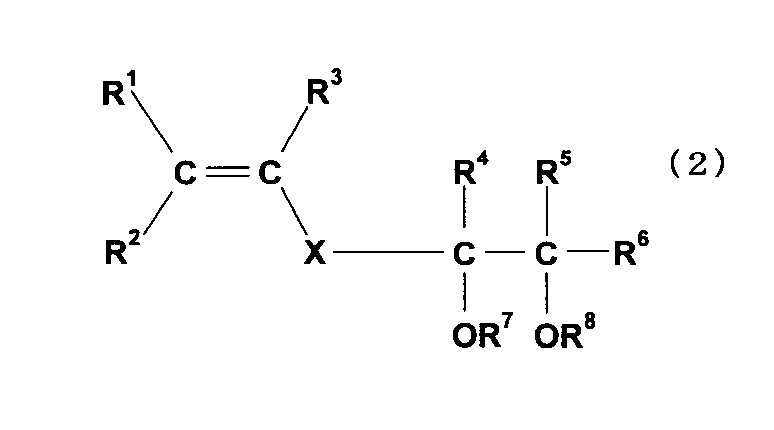
- polyvinyl alcohol resin having a 1,2-diol structural unit represented by the following general formula (1) (hereinafter, polyvinyl alcohol is abbreviated as PVA)
- PVA polyvinyl alcohol
- the inventors have found that the object of the present invention can be achieved by a coating solution for impurity diffusion containing A), impurities (B), and water (C), thereby completing the present invention.
- the present invention relates to a specific structure having a 1,2-diol structure in the side chain as a PVA resin in an impurity diffusion coating solution containing PVA resin, impurities such as phosphorus compounds and boron compounds, and water.
- the greatest feature is to use a unit.
- the impurity diffusion coating solution of the present invention is excellent in stability, when used for screen printing, it is possible to perform continuous printing for a long time and printing with a pause period, especially during pattern printing of solar cells and the like. However, since good printing accuracy can be obtained for a long time, it is extremely useful industrially.
- the coating solution for impurity diffusion of the present invention contains a PVA resin (A) having a structural unit represented by the general formula (1), impurities (B) such as phosphorus compounds and boron compounds, and water. To do.
- PVA resin A having a structural unit represented by the general formula (1)
- impurities B such as phosphorus compounds and boron compounds
- the PVA resin used in the impurity diffusion coating solution of the present invention has a structural unit represented by the following general formula (1), and R 1 , R 2 , and R 3 in the general formula (1) are independent of each other.
- X represents a single bond or a bond chain, and R 4 , R 5 , and R 6 each independently represent a hydrogen atom or an organic group.
- R 1 to R 3 and R 4 to R 6 in the 1,2-diol structural unit represented by the general formula (1) are all hydrogen atoms and X is a single bond.
- a PVA resin having a structural unit represented by the general formula (1 ′) is preferably used.
- R 1 to R 3 and R 4 to R 6 in the structural unit represented by the general formula (1) may be organic groups as long as they do not significantly impair the resin characteristics.
- the organic group include an alkyl group having 1 to 4 carbon atoms such as a methyl group, an ethyl group, an n-propyl group, an isopropyl group, an n-butyl group, an isobutyl group, and a tert-butyl group. May have a functional group such as a halogen group, a hydroxyl group, an ester group, a carboxylic acid group, or a sulfonic acid group, if necessary.
- X in the 1,2-diol structural unit represented by the general formula (1) is most preferably a single bond from the viewpoint of thermal stability or stability under high temperature or acidic conditions.
- a bonded chain may be used as long as it does not inhibit the effects of the present invention.
- Examples of such a bonded chain include hydrocarbons such as alkylene, alkenylene, alkynylene, phenylene, and naphthylene (these hydrocarbons include fluorine, chlorine, bromine, and the like).
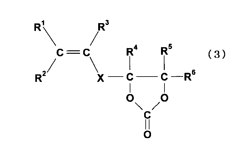
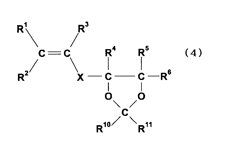
- -O of may be substituted by a halogen) -, - (CH 2 O ) m -, - (OCH 2) m -, - (CH 2 O) m CH 2 -, - CO-, —COCO—, —CO (CH 2 ) m CO—, —CO (C 6 H 4 ) CO—, —S—, —CS—, —SO—, —SO 2 —, —NR—, —CONR—, -NRCO -, - CSNR -, - NRCS -, - NRNR -, - HPO 4 -, - i (OR) 2 -, - OSi (OR) 2 -, - OSi (OR) 2 O -, - Ti (OR) 2 -, - OTi (OR) 2 -, - OTi (OR) 2 O -, - Al (OR)-, -OAl (OR)-, -,
- R is each independently an arbitrary substituent, preferably a hydrogen atom or an alkyl group, and m is a natural number. ).
- R 1 , R 2 , R 3 , X, R 4 , R 5 and R 6 are all the same as in the general formula (1).
- R 7 and R 8 are each independently a hydrogen atom or R 9 —CO— (wherein R 9 is an alkyl group).
- R 10 and R 11 are each independently a hydrogen atom or an alkyl group.
- the method described in JP-A-2006-95825 can be used.
- 3,4-diacyloxy-1-butene as the compound represented by the general formula (2) in the method (i) from the viewpoint of excellent copolymerization reactivity and industrial handleability.
- 3,4-diacetoxy-1-butene is preferably used.
- 3,4-diacetoxy-1-butene is a by-product generated when saponifying the copolymer, and a by-product generated during the saponification is derived from a structural unit derived from vinyl acetate frequently used as a vinyl ester monomer. It is an industrially significant advantage that it is the same as the resulting compound, and it is not necessary to provide any special equipment or process for the subsequent treatment or solvent recovery system, and conventional equipment can be used.
- 3,4-diacetoxy-1-butene is synthesized, for example, by an epoxy butene derivative described in WO00 / 24702, USP 5,623,086, USP 6,072,079, or the like, It can be produced by a reaction in which 1,4-diacetoxy-1-butene, which is an intermediate product of the butanediol production process, is isomerized using a metal catalyst such as palladium chloride. At the reagent level, Across products can be obtained from the market.
- the PVA-based resin obtained by the method (ii) or (iii) is insufficiently decarboxylated or deacetalized, a carbonate ring or acetal ring remains in the side chain, and heat drying during production In the process, the cyclic group may cause the PVA resin to be cross-linked to generate a gel-like material. Therefore, also from this point, the PVA resin obtained by the method (i) is preferably used in the present invention.
- vinyl ester monomers examples include vinyl formate, vinyl acetate, vinyl propionate, vinyl valelate, vinyl butyrate, vinyl isobutyrate, vinyl pivalate, vinyl caprate, vinyl laurate, vinyl stearate, vinyl benzoate, versatic. Although vinyl acid acid etc. are mentioned, vinyl acetate is preferably used economically.
- ⁇ -olefins such as ethylene and propylene
- hydroxy group-containing ⁇ -olefins such as 3-buten-1-ol, 4-penten-1-ol and 5-hexene-1,2-diol, and acylated products thereof, etc.
- Unsaturated acids such as itaconic acid, maleic acid, acrylic acid or salts thereof or mono- or dialkyl esters; nitriles such as acrylonitrile, amides such as methacrylamide, diacetone acrylamide, ethylene sulfonic acid, allyl sulfonic acid, meta Compounds such as allyl sulfonic acid, olefin sulfonic acid such as AMPS or its salts, etc. It may be copolymerized.
- the degree of saponification (measured in accordance with JIS K6726) of the PVA resin (A) used in the present invention is usually 60 to 100 mol%, particularly 70 to 99.9 mol%, and further 80 to 99. Those having 9 mol%, particularly 90 to 99.9 mol%, particularly 98 to 99.8 mol% are preferably used. If the saponification degree is too low, the solubility of the PVA-based resin in water may be reduced, and it may be difficult to obtain a uniform coating solution.
- the average degree of polymerization (measured in accordance with JIS K6726) of the PVA resin (A) is usually 100 to 4000, particularly 200 to 2000, and more preferably 300 to 1500. If the average degree of polymerization is too small, the coating solution may have a low viscosity, and it may be difficult to perform good screen printing, or the coating film may become a thin film, resulting in a shortage of impurity supply. On the other hand, if it is too large, it is unsuitable for screen printing and tends to cause printing defects.
- the content of the 1,2-diol structural unit contained in the PVA resin (A) is usually 0.5 to 30 mol%, particularly 1 to 20 mol%, more preferably 3 to 15 mol%. Used. If the content is too low, the effect of using the PVA resin (A) into which the 1,2-diol structural unit is introduced cannot be obtained. On the other hand, if the content is too high, the drying property is lowered and the productivity is reduced. There is a tendency to decrease.
- the content of the 1,2-diol structural unit in the PVA resin (A) is a 1 H-NMR spectrum (solvent: DMSO-d6, internal standard substance: tetramethyl) of a completely saponified PVA resin. Specifically, peak areas derived from hydroxyl protons, methine protons, and methylene protons in the 1,2-diol units, methylene protons in the main chain, hydroxyl protons linked to the main chain, etc. Calculate from
- the PVA resin (A) used in the present invention may be one type or a mixture of two or more types, and in that case, an unmodified PVA other than the PVA resin (A) described above.
- it may be a mixture with various modified PVA resins, but when a mixture is used, the average value of the degree of polymerization, the degree of saponification, and the content of 1,2-diol structural units may be within the above range. preferable.
- the content of the PVA resin (A) in the impurity diffusion coating solution of the present invention is usually 1 to 30% by weight, preferably 5 to 25% by weight, particularly 10 to 20% by weight. . If the content of the PVA resin (A) is too small, the viscosity of the coating solution tends to be low, and the coating film tends to be difficult to be formed stably. Conversely, if too much, the viscosity of the coating solution is high. Therefore, there is a tendency that the coating workability is deteriorated or the screen mesh is easily clogged in screen printing.
- impurity (B) used in the present invention will be described.
- an impurity (B) for example, a group 13 element compound or a group 15 element compound is used. Moreover, these compounds may be used independently and may be used together.
- the group 15 element compound is generally used as an impurity in the production of an N-type semiconductor, and examples thereof include phosphorus compounds and antimony compounds. Among these, phosphorus compounds are preferably used. Specific examples of such phosphorus compounds include phosphoric acids such as phosphoric anhydride (P 2 O 5 ) and phosphoric acid (H 3 PO 4 ), phosphates such as melamine phosphate and ammonium phosphate, acid phosphoxy methacrylate, Examples thereof include phosphoric esters such as 3-chloro-2-acid phosphooxyethyl methacrylate, acid phosphooxypolyethylene glycol monomethacrylate, and acid phosphoxypolyoxypropylene glycol monomethacrylate, and salts thereof, phosphorus chloride, and the like. Of these, water-soluble ones are preferable, and phosphoric acids are particularly preferably used. Such phosphorus compounds and the like may be used alone or in combination of two or more.
- the content of the group 15 element compound in the coating solution for impurity diffusion of the present invention is usually from 0.1 to 30% by weight, particularly from 0.1 to 10% by weight, particularly from 0.1 to 5% by weight. Is preferably used.
- the content of the Group 15 element compound with respect to 100 parts by weight of the PVA resin (A) is usually 1 to 300 parts by weight, particularly 3 to 200 parts by weight, particularly 5 to 50 parts by weight. If the content of the Group 15 element compound is small, the content of the Group 15 element (phosphorus or the like) in the impurity diffusion layer is small, and a sufficient resistance value may not be obtained. Moreover, when there is too much content of 15 group element compound, the solubility of PVA-type resin (A) may become inadequate.
- the group 13 element compound is generally used as an impurity in the production of a P-type semiconductor, and examples thereof include boron compounds and aluminum compounds.
- boron compounds are preferably used, and specific examples of such boron compounds include boric acid, boric anhydride, boron trifluoride, boron trichloride, boron tribromide, boron triiodide, trimethyl borate, boron nitride, Ammonium tetraborate (hydrate), alkyl borate ester, melamine borate, 9-BBN and the like can be mentioned.
- water-soluble ones are preferable, and boric acid and boric anhydride are particularly preferably used.
- Such boron compounds and the like may be used alone or in combination of two or more.
- the content of the group 13 element compound in the coating solution for impurity diffusion of the present invention is usually from 0.1 to 30% by weight, particularly from 0.1 to 10% by weight, particularly from 0.1 to 5% by weight. Is preferably used. Further, the content of the group 13 element compound with respect to 100 parts by weight of the PVA resin (A) is usually 5 to 50 parts by weight, particularly 10 to 40 parts by weight. If the content of the group 13 element compound is too small, the content of the group 13 element (boron or the like) in the impurity diffusion layer becomes small, and a sufficient resistance value may not be obtained. Moreover, when there is too much content of a group 13 element compound, the solubility of PVA-type resin (A) may become inadequate.
- the water (C) used in the impurity diffusion coating solution of the present invention is preferably one having few impurities such as alkali metals and heavy metals and foreign matter, and most preferably ultrapure water, but ion-exchanged water or distilled water is used. It is also possible.
- the content of water (C) in the coating solution for impurity diffusion of the present invention is usually 20 to 85% by weight, preferably 30 to 80% by weight, particularly 40 to 75% by weight. If the content of water (C) is too small, the viscosity of the coating solution tends to be too high, and the coating workability tends to decrease, or the screen mesh tends to be clogged during screen printing. On the other hand, if the amount is too large, the viscosity may be too low and the coating film may not be stably formed, or the impurity content in the impurity diffusion layer may be too small.
- Alcohols (D) It is preferable that an alcohol (D) is further blended in the impurity diffusion coating solution of the present invention. By blending such alcohols, it is possible to improve the storage stability and flow stability of the coating liquid and the leveling property of the coating film.
- alcohols (D) include monohydric alcohols such as methanol (65 ° C.), ethanol (78 ° C.), isopropanol (82 ° C.); ethylene glycol (197 ° C.), diethylene glycol (244 ° C.) Dihydric alcohols such as triethylene glycol (287 ° C.), tetraethylene glycol (314 ° C.), propylene glycol (188 ° C.); glycerin (290 ° C.), trimethylolpropane (292 ° C.), sorbitol (296 ° C.), Trivalent or higher polyhydric alcohols such as mannitol (290 to 295 ° C.), pentaerythritol (276 ° C.), polyglycerin; and ethylene glycol monomethyl ether (124 ° C.), ethylene glycol nomoethyl ether (136 ° C.), ethylene Glycolmo -n- butyl ether (171
- alcohols having a boiling point higher than that of water that is, a boiling point of 100 ° C. or higher, in that rapid drying of the coated film after printing is suppressed and the leveling property is greatly improved.
- Those having a temperature of -350 ° C, particularly 200-300 ° C are preferably used.
- the blending amount of the alcohol (D) blended in the impurity diffusion coating solution of the present invention is usually 5 to 70 parts by weight, particularly 10 to 60 parts by weight, particularly 30 to 30 parts by weight based on the total amount of the coating solution. A range of 50 parts by weight is preferably used.
- the blending amount of the alcohol (D) with respect to 100 parts by weight of water (C) is usually 5 to 200 parts by weight, particularly 20 to 150 parts by weight, particularly 80 to 120 parts by weight. If the content of the alcohol (D) is too small, the fluidity improving effect and the leveling effect cannot be obtained sufficiently. Is not preferred, and when high-boiling alcohols are used, drying tends to require a high temperature and a long time.
- a surfactant (E) is further added to the impurity diffusion coating solution of the present invention.
- a surfactant By blending such a surfactant, wettability to the semiconductor surface is improved, foaming of the coating liquid is suppressed, and printing defects due to bubbles can be prevented.
- Surfactants used in aqueous liquids can be broadly classified into nonionic surfactants, cationic surfactants, and anionic surfactants, and any of them can be used. Therefore, nonionic surfactants are preferable. As such nonionic surfactants, known ones can be used.
- hydrocarbon surfactants such as block copolymers of ethylene oxide-propylene oxide, acetylene glycol derivatives, silicon -Based surfactants, fluorine-based surfactants and the like.
- hydrocarbon surfactants, particularly acetylene glycol derivatives are preferably used because they are excellent in suppressing foaming and defoaming in the coating solution of the present invention.
- acetylene glycol derivatives those represented by the following formula (5) are preferably used.
- R 12 and R 15 each independently represents an alkyl group having 1 to 20 carbon atoms, preferably having 1 to 5 carbon atoms, particularly preferably having 3 to 5 carbon atoms.
- R 13 and R 14 each independently represents an alkyl group having 1 to 3 carbon atoms, and a methyl group is particularly preferably used.
- R 12 and R 15 and R 13 and R 14 may be the same or different, but those having the same structure are preferably used.
- n and m are each an integer of 0 to 30, and those in which m + n is 1 to 10, particularly 1 to 5, particularly 1 to 3 are preferably used.
- acetylene glycol derivatives include 2,5,8,11-tetramethyl-6-dodecin-5,8-diol ethylene oxide adduct, 5,8-dimethyl-6-dodecin-5,8. -Ethylene oxide adduct of diol, ethylene oxide adduct of 2,4,7,9-tetramethyl-5-decyne-4,7-diol, 4,7-dimethyl-5-decyne-4,7-diol Ethylene oxide adduct, 2,3,6,7-tetramethyl-4-octyne-3,6-diol ethylene oxide adduct, 3,6-dimethyl-4-octyne-3,6-diol ethylene oxide addition And an ethylene oxide adduct of 2,5-dimethyl-3-hexyne-2,5-diol. Among these, ethylene oxide adducts of 2,4,7,9-tetramethyl-6-
- Examples of such commercially available surfactants that are acetylene glycol derivatives include Surfynol series manufactured by Nissin Chemical Industry Co., Ltd.
- the amount of the surfactant (E) blended in the impurity diffusion coating solution of the present invention is usually from 0.1 to 10% by weight, particularly from 0.3 to 8% by weight, especially from 0 to 0%, in the coating solution.
- the range of 5 to 5% by weight is preferably used. If the blending amount of the surfactant (E) is too small, the foam suppression / defoaming effect may be insufficient. On the other hand, if the amount is too large, it may be separated from the liquid and a uniform solution may not be obtained.
- inorganic fine particles can be blended in the impurity diffusion coating solution of the present invention.
- inorganic fine particles silicas such as colloidal silica, amorphous silica, and fumed silica are suitable, and among them, colloidal silica is preferably used.
- the blending amount of such inorganic fine particles is usually 0.5 to 20% by weight in the coating solution, and particularly preferably in the range of 1 to 10% by weight.
- the coating solution for impurity diffusion of the present invention contains the above-mentioned PVA resin (A), impurity (B), and water (C), and if necessary, further alcohols (D), surface activity. Agent (E) and other additives are blended.
- the viscosity at 20 ° C. of such an impurity diffusion coating solution is usually 300 to 100,000 mPa ⁇ s, preferably 500 to 10,000 mPa ⁇ s, particularly 700 to 6,000 mPa ⁇ s. In addition, this viscosity is measured using a B-type viscometer. If the concentration and viscosity of the coating solution are too small, the coating film may not be stably formed or the content of phosphorus, boron, etc. in the impurity diffusion layer may be insufficient. If the viscosity is too large, the coating workability tends to be reduced, or the screen mesh is easily clogged during screen printing.
- the impurity diffusion coating solution of the present invention is obtained by dissolving the PVA resin (A) and the impurity (B) described above in water (C), to which an alcohol compound (D), a surfactant (E), and inorganic fine particles are dissolved. It can prepare by mix
- this preparation method after making PVA-type resin (A) into aqueous solution, the method of mix
- a method of adding this additive to water (C), mixing with other additives after heating and stirring with stirring, and the like can be mentioned, but it is not limited thereto.
- the impurity diffusion coating solution of the present invention thus obtained is excellent in storage stability, so it can be prepared and stored in large quantities, moved in small portions, or used halfway to store the rest. It is also possible to do.
- the impurity diffusion coating solution of the present invention is applied to a semiconductor substrate such as silicon or germanium, and a diffusion layer such as phosphorus or boron is formed in the semiconductor substrate through drying, baking, and diffusion steps. It is manufactured by.
- a known method can be used as a method for applying the impurity diffusion coating solution on the semiconductor substrate. Specifically, a screen printing method, a gravure printing method, a relief printing method, a lithographic printing method, a spin coater method. , Comma coater method, die head coater method, die lip coater method, and the like.
- the coating liquid of the present invention is most effective when used in a screen printing method, and a uniform coating film can be obtained even on a large wafer of 4 inches or more.
- the coating amount of the coating solution on the semiconductor substrate varies depending on the type of the substrate, the use of the semiconductor, the content of impurities (phosphorus compound, boron compound, etc.) in the coating solution, and the desired phosphorus content, boron content, etc. Is usually 1 to 100 g / m 2 , in particular 1 to 50 g / m 2 .
- volatile components such as water are removed from the coating film, and the conditions may be set as appropriate.
- the temperature is 20 to 300 ° C., particularly 100 to 200 ° C. Minutes, in particular 5 to 30 minutes, are used.
- the drying method is not particularly limited, and a known method such as hot air drying, infrared heat drying, or vacuum drying can be used.
- the subsequent firing step (degreasing step) most of the organic components in the coating film are removed using an electric furnace or the like.
- the conditions of such a process need to be adjusted as appropriate depending on the composition of the coating solution and the thickness of the coating film, but are usually 300 to 1000 ° C., particularly 400 to 800 ° C., 1 to 120 minutes, particularly 5 to 60. Implemented in minutes. Further, phosphorus, boron, etc. are diffused in the semiconductor substrate in the diffusion process, and an impurity diffusion layer is formed.
- using an electric furnace or the like under the temperature condition of 800-1400 ° C., It is performed in a state where a plurality of sheets are overlapped. Note that it is possible to omit the diffusion step when the firing step and the diffusion step are performed in one step, or when diffusion proceeds in the baking step and a desired resistance value is obtained.
- the surface resistance of such semiconductors can be controlled by the impurity content, diffusion temperature, diffusion time, etc., and usually has a surface resistance in the range of 0.03 to 10000 ⁇ / ⁇ suitable for the intended use. It is possible to obtain.
- the methanol solution was further diluted with methanol, adjusted to a concentration of 40%, charged into a kneader, and sodium hydroxide was used as a 2% methanol solution while keeping the solution temperature at 40 ° C.
- Saponification was carried out by adding 8 mmol to the total amount of 1 mol of the unit and 3,4-diacetoxy-1-butene structural unit. As saponification progressed, when saponified substances were precipitated and formed into particles, they were separated by filtration, washed well with methanol, and dried in a hot air drier to prepare the intended PVA resin (A1).
- the degree of saponification of the obtained PVA resin (A1) was 99.8 mol% when analyzed by the alkali consumption required for hydrolysis of residual vinyl acetate and 3,4-diacetoxy-1-butene. .
- the average degree of polymerization was 350 when analyzed according to JIS K 6726.
- the content of the 1,2-diol structural unit represented by the general formula (1) is 1 H-NMR (300 MHz proton NMR, DMSO-d6 solution, internal standard substance: tetramethylsilane, 50 ° C.). It was 8 mol% when calculated from the measured integrated value (see Table 1).
- the methanol solution was further diluted with methanol, adjusted to a concentration of 35%, charged into a kneader, and sodium hydroxide was used as a 2% methanol solution while maintaining the solution temperature at 35 ° C.
- the vinyl acetate structure in the copolymer Saponification was carried out by adding 8 mmol to the total amount of 1 mol of the unit and 3,4-diacetoxy-1-butene structural unit. As saponification progressed, when saponified substances were precipitated and formed into particles, they were separated by filtration, washed well with methanol, and dried in a hot air dryer to prepare the intended PVA resin (A2).
- the degree of saponification of the obtained PVA resin (A2) was 99.6 mol% when analyzed by the alkali consumption required for hydrolysis of residual vinyl acetate and 3,4-diacetoxy-1-butene. .
- the average degree of polymerization was 470 when analyzed according to JIS K 6726.
- the content of the 1,2-diol structural unit represented by the general formula (1) is 1 H-NMR (300 MHz proton NMR, DMSO-d6 solution, internal standard substance: tetramethylsilane, 50 ° C.). It was 12 mol% when calculated from the measured integral value (see Table 1).
- the methanol solution was further diluted with methanol, adjusted to a concentration of 30%, charged into a kneader, and the solution temperature was kept at 35 ° C., and sodium hydroxide was used as a 2% methanol solution to form a vinyl acetate structure in the copolymer.
- Saponification was carried out by adding 8 mmol to the total amount of 1 mol of the unit and 3,4-diacetoxy-1-butene structural unit. As saponification progressed, when saponified substances were precipitated and formed into particles, they were separated by filtration, washed well with methanol, and dried in a hot air dryer to prepare the intended PVA resin (A3).
- the degree of saponification of the obtained PVA resin (A3) was 99.7 mol% when analyzed by the alkali consumption required for hydrolysis of residual vinyl acetate and 3,4-diacetoxy-1-butene. .
- the average degree of polymerization was 1200 when analyzed according to JIS K 6726.
- the content of the 1,2-diol structural unit represented by the general formula (1) is 1 H-NMR (300 MHz proton NMR, DMSO-d6 solution, internal standard substance: tetramethylsilane, 50 ° C.). It was 6 mol% when computed from the measured integral value (refer Table 1).
- Example 1 Preparation of coating solution for phosphorus diffusion> 17 g of the PVA resin (A1) obtained in Production Example 1 was added to 40.5 g of ultrapure water (C), and dissolved while stirring under heating to prepare Solution A. Further, 40 g of glycerin is used as the alcohol (D), and ethylene oxide of 2,4,7,9-tetramethyl-5-decyne-4,7-diol, which is an acetylene glycol derivative, is used as the surfactant (E). 1.5 g of an adduct (m + n ⁇ 1.3 in the general formula (1)) was added to prepare a solution B.
- an adduct m + n ⁇ 1.3 in the general formula (1)
- the semiconductor substrate on which the phosphorous diffusion coating solution of the present invention was screen-printed was dried in a hot air circulating dryer at 150 ° C. for 2 minutes, then placed in a 900 ° C. muffle furnace, held for 15 minutes, taken out, and 46% fluorinated.
- the semiconductor substrate was cleaned while being swung in an aqueous hydrogen solution to obtain a semiconductor having a phosphorus diffusion layer in the semiconductor substrate.
- the surface resistance value at the center position of the 30 mm square pattern of the obtained semiconductor was measured using a resistance measuring instrument (“Lorestar” manufactured by Mitsubishi Analytech Co., Ltd., using a PSP probe). The results are shown in Table 3.
- Example 2 In Example 1, the PVA-based resin (A2) obtained in Production Example 2 was used as the PVA-based resin (A), and the amount of each component was as shown in Table 2 and was the same as in Example 1.
- a phosphorus diffusion coating solution was prepared and evaluated in the same manner. Table 2 shows the viscosity of the coating solution, and Table 3 shows the evaluation results. Moreover, the semiconductor using this coating liquid was produced similarly, and evaluated similarly. The results are shown in Table 3.
- Example 1 In Example 1, unmodified PVA (a1) (polymerization degree 320, saponification degree 98.3 mol%) and unmodified PVA (a2) (polymerization degree 450, saponification degree 87.5 mol%) as PVA-based resins ), And a phosphorus diffusion coating solution was prepared and evaluated in the same manner as in Example 1 except that the amount of each component was as shown in Table 2.
- Table 2 shows the viscosity of the coating solution, and Table 3 shows the evaluation results.
- the semiconductor using this coating liquid was produced similarly, and evaluated similarly. The results are shown in Table 3.
- Example 3 In Example 1, the PVA resin (A3) obtained in Production Example 3 was used as the PVA resin (A), niline pentoxide was used as the phosphorus compound (B), and methyl carbitol was used as the alcohol (D).
- a coating solution for phosphorus diffusion was prepared and evaluated in the same manner as in Example 1 except that the surfactant (E) was not used and the amount of each component was as shown in Table 2.
- Table 2 shows the viscosity of the coating solution, and Table 3 shows the evaluation results.
- the semiconductor using this coating liquid was produced similarly, and evaluated similarly. The results are shown in Table 3.
- Example 4 In Example 1, the PVA resin (A3) obtained in Production Example 3 was used as the PVA resin (A), the alcohols (D) and the surfactant (E) were not blended, and the blending amounts of the respective components
- a phosphorus diffusion coating solution was prepared in the same manner as in Example 1 except that the values were as shown in Table 2, and evaluated in the same manner.
- Table 2 shows the viscosity of the coating solution
- Table 3 shows the evaluation results.
- the semiconductor using this coating liquid was produced similarly, and evaluated similarly. The results are shown in Table 3.
- the phosphorus diffusion coating solution of the present invention obtained excellent printability even after being left for a certain time in screen printing.
- the initial printability was good, but when printing was performed after being left, the pattern was chipped.
- the semiconductors obtained using the phosphorous diffusion coating solution of the present invention all had high surface resistance values.
- Example 5 Preparation of boron diffusion coating solution> 18 g of the PVA resin (A1) obtained in Production Example 1 was added to 44 g of ultrapure water (C), and dissolved while stirring under heating to prepare Solution A. Further, 34 g of glycerin is used as the alcohol (D), and ethylene oxide of 2,4,7,9-tetramethyl-5-decyne-4,7-diol, which is an acetylene glycol derivative, is used as the surfactant (E). A solution B was prepared by adding 1.8 g of an adduct (m + n ⁇ 1.3 in the general formula (1)). Boron acid (2.2 g) was added to the solution A as a boron compound (B), and the solution B was further added and stirred to prepare a boron diffusion coating solution. The composition and viscosity of the coating solution obtained are as shown in Table 4.
- the semiconductor substrate on which the boron diffusion coating solution of the present invention was screen-printed was dried in a hot air circulating dryer at 150 ° C. for 2 minutes, then placed in a muffle furnace at 950 ° C., held for 15 minutes, taken out, and 46% fluorinated.
- the semiconductor substrate was washed while being swung in an aqueous hydrogen solution to obtain a semiconductor having a boron diffusion layer in the semiconductor substrate.
- the surface resistance value at the center position of the 30 mm square pattern of the obtained semiconductor was measured using a resistance measuring instrument (“Lorestar” manufactured by Mitsubishi Analytech Co., Ltd., using a PSP probe). The results are shown in Table 5.
- Example 6 In Example 5, 54 g of ultrapure water (C) was used, 7 g of the PVA resin (A3) obtained in Production Example 3 was used as the PVA resin (A), and 35 g of methyl carbitol was used as the alcohol (D).
- a boron diffusion coating solution was prepared and evaluated in the same manner as in Example 5 except that it was used. The composition and viscosity of the coating solution are shown in Table 4, and the evaluation results are shown in Table 5. Moreover, the semiconductor using this coating liquid was produced similarly, and evaluated similarly. The results are shown in Table 5.
- Example 5 Comparative Example 3 In Example 5, 47 g of ultrapure water (C) was used, and 15 g of unmodified PVA (a1) (polymerization degree 320, saponification degree 98.3 mol%) was used as the PVA resin. An attempt was made to prepare a boron diffusion coating solution, but it gelled during preparation.
- Example 5 In Example 5, 47.4 g of ultrapure water (C) was used, 13.6 g of unmodified PVA (a2) (polymerization degree 450, saponification degree 87.5 mol%) was used as the PVA resin, and alcohols (A coating solution for boron diffusion was prepared and evaluated in the same manner as in Example 5 except that 35 g of methyl carbitol was used as D). The composition and viscosity of the coating solution are shown in Table 4, and the evaluation results are shown in Table 5. Moreover, the semiconductor using this coating liquid was produced similarly, and evaluated similarly. The results are shown in Table 5.
- the coating solution for impurity diffusion of the present invention is excellent in stability, and can be used for continuous printing for a long time when subjected to screen printing. In some cases, the printing accuracy is kept good for a long time, which is extremely useful industrially.
Abstract
Description
そこで、大型ウェハーにも対応可能な塗布法としてスクリーン印刷法が検討され、かかる印刷法に好適な不純物含有拡散用塗布液が提案されている。(例えば、特許文献1、2参照。)

以下、本発明について詳細に説明する。
以下、各順に説明する。
まず、本発明で用いられるPVA系樹脂(A)について説明する。
本発明の不純物拡散用塗布液に用いられるPVA系樹脂は、下記一般式(1)で示される構造単位を有するもので、一般式(1)におけるR1、R2、及びR3はそれぞれ独立して水素原子または有機基を示し、Xは単結合または結合鎖を示し、R4、R5、及びR6はそれぞれ独立して水素原子または有機基を示すものである。


なかでも、共重合反応性および工業的な取り扱い性に優れるという点から、(i)の方法において、一般式(2)で表わされる化合物として3,4-ジアシロキシ-1-ブテンを用いることが好ましく、特に3,4-ジアセトキシ-1-ブテンが好ましく用いられる。
なお、ビニルエステル系モノマーとして酢酸ビニルを用い、これと3,4-ジアセトキシ-1-ブテンを共重合させた際の各モノマーの反応性比は、r(酢酸ビニル)=0.710、r(3,4-ジアセトキシ-1-ブテン)=0.701、であり、これは(ii)の方法で用いられる一般式(3)で表される化合物であるビニルエチレンカーボネートの場合の、r(酢酸ビニル)=0.85、r(ビニルエチレンカーボネート)=5.4、と比較して、3,4-ジアセトキシ-1-ブテンが酢酸ビニルとの共重合反応性に優れることを示すものである。
また、試薬レベルではアクロス社の製品を市場から入手することができる。
よって、かかる点からも、(i)の方法によって得られたPVA系樹脂が本発明においては好適に用いられる。
また上述のモノマー(ビニルエステル系モノマー、一般式(2)、(3)、(4)で示される化合物)の他に、樹脂物性に大幅な影響を及ぼさない範囲であれば、共重合成分として、エチレンやプロピレン等のαーオレフィン;3-ブテン-1-オール、4-ペンテン-1-オール、5-ヘキセン-1,2-ジオール等のヒドロキシ基含有α-オレフィン類、およびそのアシル化物などの誘導体;イタコン酸、マレイン酸、アクリル酸等の不飽和酸類あるいはその塩あるいはモノ又はジアルキルエステル;アクリロニトリル等のニトリル類、メタクリルアミド、ジアセトンアクリルアミド等のアミド類、エチレンスルホン酸、アリルスルホン酸、メタアリルスルホン酸、AMPS等のオレフィンスルホン酸あるいはその塩などの化合物、などが共重合されていてもよい。
かかる平均重合度が小さすぎると塗布液が低粘度となり、良好なスクリーン印刷が困難となったり、塗膜が薄膜となり、不純物の供給量が不足する場合がある。逆に大きすぎてもスクリーン印刷には不適であり、印刷不良が発生しやすくなる傾向がある。
かかるPVA系樹脂(A)の含有量が小さすぎると、塗布液の粘度が低くなり、塗膜が安定して形成されにくくなる傾向があり、逆に、多すぎると、塗布液の粘度が高くなるため、塗布作業性が低下したり、スクリーン印刷におけるスクリーンメッシュの目詰まりが起りやすくなる傾向がある。
次に、本発明で用いられる不純物(B)について説明する。
かかる不純物(B)としては、例えば、13族元素化合物や15族元素化合物が用いられる。また、これらの化合物は、単独で用いてもよく、併用してもよい。
なお、かかるリン化合物等は、単独で用いてもよく、二種以上のものを組合わせて用いてもよい。
また、15族元素化合物のPVA系樹脂(A)100重量部に対する含有量は、通常1~300重量部であり、特に3~200重量部、殊に5~50重量部の範囲が用いられる。
かかる15族元素化合物の含有量が小さいと、不純物拡散層中の15族元素(リン等)の含有量が小さくなり、充分な抵抗値が得られない場合がある。また、15族元素化合物の含有量が多すぎると、PVA系樹脂(A)の溶解性が不充分となる場合がある。
なお、かかるホウ素化合物等は、単独で用いてもよく、二種以上のものを組合わせて用いてもよい。
また、13族元素化合物のPVA系樹脂(A)100重量部に対する含有量は、通常5~50重量部であり、特に10~40重量部の範囲が用いられる。
かかる13族元素化合物の含有量が少なすぎると、不純物拡散層中の13族元素(ホウ素等)の含有量が小さくなり、充分な抵抗値が得られない場合がある。また、13族元素化合物の含有量が多すぎると、PVA系樹脂(A)の溶解性が不充分となる場合がある。
本発明の不純物拡散用塗布液に用いられる水(C)としては、アルカリ金属や重金属などの不純物、および異物が少ないものが好ましく、超純水が最も好ましいが、イオン交換水、蒸留水を用いることも可能である。
本発明の不純物拡散用塗布液における水(C)の含有量は、通常20~85重量%であり、特に30~80重量%、殊に40~75重量%の範囲が好ましく用いられる。かかる水(C)の含有量が少なすぎると、塗布液の粘度が高くなりすぎ、塗布作業性が低下したり、スクリーン印刷におけるスクリーンメッシュの目詰まりが起りやすくなる傾向がある。逆に多すぎると粘度が低くなりすぎて塗膜が安定して形成されにくくなったり、不純物拡散層中の不純物の含有量が小さくなりすぎる場合がある。
本発明の不純物拡散用塗布液には、さらに、アルコール類(D)を配合することが好ましい。かかるアルコール類を配合することによって、塗布液の保存安定性や流動安定性、塗布膜のレベリング性を改善することが可能である。
かかるアルコール類(D)としては、具体的には、メタノール(65℃)、エタノール(78℃)、イソプロパノール(82℃)などの一価アルコール類;エチレングリコール(197℃)、ジエチレングリコール(244℃)、トリエチレングリコール(287℃)、テトラエチレングリコール(314℃)、プロピレングリコール(188℃)などのニ価アルコール類;グリセリン(290℃)、トリメチロールプロパン(292℃)、ソルビトール(296℃)、マンニトール(290~295℃)、ペンタエリスリトール(276℃)、ポリグリセリンなどの三価以上の多価アルコール類;および、エチレングリコールモノメチルエーテル(124℃)、エチレングリコールノモエチルエーテル(136℃)、エチレングリコールモノ-n-ブチルエーテル(171℃)、プロピレングリコールモノメチルエーテル(120℃)、ジエチレングリコールモノメチルエーテル(メチルカルビトール)(194℃)などのアルコール誘導体を挙げることができる。なお、( )内の値は沸点である。
これらは単独で用いても良く、二種以上を併用しても良い。
また、アルコール類(D)の水(C)100重量部に対する配合量は、通常5~200重量部であり、特に20~150重量部、殊に80~120重量部の範囲が好ましく用いられる。かかるアルコール類(D)の含有量が少なすぎると流動性の改善効果、およびレベリング効果が充分得られなくなり、逆に多すぎるとPVA系樹脂(A)の溶解性が低下し、均一な塗布液が得られなくなったり、高沸点のアルコール類を用いた場合には乾燥に高温、長時間を要する傾向があるため、好ましくない。
本発明の不純物拡散用塗布液には、さらに、界面活性剤(E)を配合することが好ましい実施態様である。かかる界面活性剤を配合することによって、半導体表面への濡れ性が向上し、さらに塗布液の発泡が抑制され、気泡に起因する印刷不良を防止することが可能となる。
水性液に用いられる界面活性剤は、ノニオン系界面活性剤、カチオン系界面活性剤、アニオン系界面活性剤に大別でき、いずれも使用することができるが、半導体への金属成分等の持込が少ないことから、ノニオン系界面活性剤が好ましい。
かかるノニオン系界面活性剤としては、公知のものを使用することが可能であり、具体的にはエチレンオキサイド-プロピレンオキサイドのブロック共重合体、アセチレングリコール誘導体などの炭化水素系界面活性剤や、シリコン系界面活性剤、フッ素系界面活性剤などを挙げることができる。
中でも、本発明の塗布液において発泡の抑制、および消泡性に優れている点で、炭化水素系界面活性剤、特にアセチレングリコール誘導体が好ましく用いられる。

また、n,mはそれぞれ0~30の整数であり、特にm+nが1~10、特に1~5、殊に1~3であるものが好ましく用いられる。
これらの中でも、2,4,7,9-テトラメチル-5-デシン-4,7-ジオールのエチレンオキサイド付加物であって、エチレンオキサイドの付加量(m+n)が1~2であるものが好ましく用いられる。
本発明の不純物拡散用塗布液には、スクリーン印刷特性を改善する目的で、各種の無機微粒子を配合することが可能である。
かかる無機微粒子としては、コロイダルシリカ、非晶質シリカ、フュームドシリカなどのシリカ類が好適であり、中でもコロイダルシリカが好ましく用いられる。
かかる無機微粒子の配合量は、通常、塗布液中0.5~20重量%であり、特に1~10重量%の範囲が好ましく用いられる。
本発明の不純物拡散用塗布液は、上述のPVA系樹脂(A)、不純物(B)、および水(C)を含有するものであり、必要に応じて、さらにアルコール類(D)、界面活性剤(E)、およびその他の添加剤を配合してなるものである。
かかる不純物拡散用塗布液の20℃における粘度は通常300~100,000mPa・sであり、特に500~10,000mPa・s、殊に700~6,000mPa・sの範囲が好ましく用いられる。なお、かかる粘度はB型粘度計を用いた測定したものである。
かかる塗布液の濃度、および粘度が小さすぎると塗膜が安定して形成されにくくなったり、不純物拡散層中のリンやホウ素等の含有量が不充分になる場合があり、逆に濃度、および粘度が大きすぎると、塗布作業性が低下したり、スクリーン印刷におけるスクリーンメッシュの目詰まりが起りやすくなる傾向がある。
次に、本発明の不純物拡散用塗布液を用いて得られる半導体について説明する。
かかる半導体は、シリコンやゲルマニウムなどの半導体基板上に本発明の不純物拡散用塗布液を塗布し、乾燥、焼成、拡散の各工程を経て、半導体基板中にリンやホウ素等の拡散層を形成することで製造される。
半導体基板上への塗布液の塗布量は、基板の種類や半導体の用途、塗布液中の不純物(リン化合物やホウ素化合物等)の含有量と、所望のリン含有量,ホウ素含有量等によって異なるが、通常、1~100g/m2であり、特に1~50g/m2の範囲で実施される。
なお、必要に応じて塗布工程と乾燥工程を連続して実施することも可能である。
さらに、拡散工程で半導体基板中にリンやホウ素等が拡散され、不純物拡散層が形成されるが、焼成工程と同様に電気炉等を用い、800~1400℃の温度条件下、枚葉、あるいは複数枚を重ね合わせた状態で行われる。
なお、焼成工程と拡散工程を一工程で実施する、あるいは、焼成工程にて拡散が進行し、所望とする抵抗値が得られる場合、拡散工程を省略することも可能である。
尚、例中、「部」、「%」とあるのは、断りのない限り重量基準を意味する。
〔PVA系樹脂(A1)の製造〕
還流冷却器、滴下漏斗、撹拌機を備えた反応容器に、酢酸ビニル1500部、メタノール800部、3,4-ジアセトキシ-1-ブテン240部を仕込み、アゾビスイソブチロニトリルを0.05モル%(対仕込み酢酸ビニル)投入し、撹拌しながら窒素気流下で温度を上昇させ、重合を開始した。酢酸ビニルの重合率が87%となった時点で、m-ジニトロベンゼンを添加して重合を終了し、続いて、メタノール蒸気を吹き込む方法により未反応の酢酸ビニルモノマーを系外に除去し共重合体のメタノール溶液とした。
〔PVA系樹脂(A2)の製造〕
還流冷却器、滴下漏斗、撹拌機を備えた反応容器に、酢酸ビニル1500部、メタノール2100部、3,4-ジアセトキシ-1-ブテン180部を仕込み、アゾビスイソブチロニトリルを0.06モル%(対仕込み酢酸ビニル)投入し、撹拌しながら窒素気流下で温度を上昇させ、重合を開始した。酢酸ビニルの重合率が80%となった時点で、m-ジニトロベンゼンを添加して重合を終了し、続いて、メタノール蒸気を吹き込む方法により未反応の酢酸ビニルモノマーを系外に除去し共重合体のメタノール溶液とした。
〔PVA系樹脂(A3)の製造〕
還流冷却器、滴下漏斗、撹拌機を備えた反応容器に、酢酸ビニル1000部、メタノール400部、3,4-ジアセトキシ-1-ブテン120部を仕込み、アゾビスイソブチロニトリルを0.06モル%(対仕込み酢酸ビニル)投入し、撹拌しながら窒素気流下で温度を上昇させ、重合を開始した。酢酸ビニルの重合率が80%となった時点で、m-ジニトロベンゼンを添加して重合を終了し、続いて、メタノール蒸気を吹き込む方法により未反応の酢酸ビニルモノマーを系外に除去し共重合体のメタノール溶液とした。
<リン拡散用塗布液の作製>
超純水(C)40.5gに製造例1で得られたPVA系樹脂(A1)17gを加え、加熱撹拌しながら溶解し、溶液Aを作製した。
また、アルコール類(D)としてグリセリン40gを用い、これに界面活性剤(E)としてアセチレングリコール誘導体である2,4,7,9-テトラメチル-5-デシン-4,7-ジオールのエチレンオキサイド付加物(一般式(1)中、m+n≒1.3)1.5gを添加して溶液Bを作製した。
かかる溶液Aにリン化合物(B)としてリン酸水溶液(関東化学社製、EL用、リン酸85重量%、水15重量%)1.2g(純分1g)を添加し、さらに溶液Bを添加、撹拌してリン拡散用塗布液を作製した。得られた塗布液の粘度は表2に示すとおりである。
半導体基板(多結晶シリコン、156mm角、200μm厚)に下記の印刷条件にてスクリーン印刷を行い、スクレッパーで版上に塗布液を供給した状態で一定時間(5、15、30分)放置した後、再度印刷を行った。得られた印刷面の状態を目視観察し、下記の評価条件にて印刷性を評価した。結果を表3に示す。
(印刷条件)
印刷機 :ニューロング精密工業社製「LS-34GX」
スキージー :ニューロング精密工業社製NMスキージー(硬度:60)
スキージー角 :80度
スクレッパー :ニューロング精密工業社製NMスキージー(硬度:60)
スクレッパー角:86度
印圧 :0.2MPa
スクリーン版 :東京プロセスサービス社製
版サイズ :450mm角
メッシュ種 :V330
乳剤種 :TN-1
乳剤厚 :10μm
パターン :L/S=80~220μm、20μm毎/L×3
30mm角のベタパターンが2箇所
印刷環境 :23℃、60%RH
(評価条件)
○:全パターンが印刷されていた。
×:パターンに欠けが認められた。
上記、本発明のリン拡散用塗布液がスクリーン印刷された半導体基板を熱風循環乾燥機中150℃で2分間乾燥した後、900℃のマッフル炉に投入、15分間ホールド後取り出し、46%フッ化水素水溶液中で揺動させながら洗浄し、半導体基板中にリンの拡散層を有する半導体を得た。
得られた半導体の30mm角パターンの中心位置の表面抵抗値を、抵抗測定器(三菱アナリテック社製「ロレスター」、PSPプローブ使用)を用いて測定した。結果を表3に示す。
実施例1において、PVA系樹脂(A)として製造例2で得られたPVA系樹脂(A2)を用い、各成分の配合量を表2に示すとおりとした以外は実施例1と同様にしてリン拡散用塗布液を作製し、同様に評価した。かかる塗布液の粘度を表2に、評価結果を表3に示す。
また、かかる塗布液を用いた半導体を同様に作製し、同様に評価した。結果を表3に示す。
実施例1において、PVA系樹脂として未変性PVA(a1)(重合度320、ケン化度98.3モル%)、および未変性PVA(a2)(重合度450、ケン化度87.5モル%)を用い、各成分の配合量を表2に示すとおりとした以外は実施例1と同様にしてリン拡散用塗布液を作製し、同様に評価した。かかる塗布液の粘度を表2に、評価結果を表3に示す。
また、かかる塗布液を用いた半導体を同様に作製し、同様に評価した。結果を表3に示す。
実施例1において、PVA系樹脂(A)として製造例3で得られたPVA系樹脂(A3)を用い、リン化合物(B)として五酸化ニリンを用い、アルコール類(D)としてメチルカルビトールを用い、界面活性剤(E)を配合せず、各成分の配合量を表2に示すとおりとした以外は実施例1と同様にしてリン拡散用塗布液を作製し、同様に評価した。かかる塗布液の粘度を表2に、評価結果を表3に示す。
また、かかる塗布液を用いた半導体を同様に作製し、同様に評価した。結果を表3に示す。
実施例1において、PVA系樹脂(A)として製造例3で得られたPVA系樹脂(A3)を用い、アルコール類(D)、界面活性剤(E)を配合せず、各成分の配合量を表2に示すとおりとした以外は実施例1と同様にしてリン拡散用塗布液を作製し、同様に評価した。かかる塗布液の粘度を表2に、評価結果を表3に示す。
また、かかる塗布液を用いた半導体を同様に作製し、同様に評価した。結果を表3に示す。


また、本発明のリン拡散用塗布液を用いて得られた半導体は、いずれも高い表面抵抗値を有するものであった。
<ホウ素拡散用塗布液の作製>
超純水(C)44gに製造例1で得られたPVA系樹脂(A1)18gを加え、加熱撹拌しながら溶解し、溶液Aを作製した。
また、アルコール類(D)としてグリセリン34gを用い、これに界面活性剤(E)としてアセチレングリコール誘導体である2,4,7,9-テトラメチル-5-デシン-4,7-ジオールのエチレンオキサイド付加物(一般式(1)中、m+n≒1.3)1.8gを添加して溶液Bを作製した。
かかる溶液Aにホウ素化合物(B)としてホウ酸2.2gを添加し、さらに溶液Bを添加、撹拌してホウ素拡散用塗布液を作製した。得られた塗布液の組成、および粘度は表4に示すとおりである。
半導体基板(多結晶シリコン、156mm角、200μm厚)に下記の印刷条件にてスクリーン印刷を行い、スクレッパーで版上に塗布液を供給した状態で一定時間(5、15分)放置した後、再度印刷を行った。得られた印刷面の状態を目視観察し、下記の評価条件にて印刷性を評価した。結果を表5に示す。
(印刷条件)
印刷機 :ニューロング精密工業社製「LS-34GX」
スキージー :ニューロング精密工業社製NMスキージー(硬度:60)
スキージー角 :80度
スクレッパー :ニューロング精密工業社製NMスキージー(硬度:60)
スクレッパー角:86度
印圧 :0.2MPa
スクリーン版 :東京プロセスサービス社製
版サイズ :450mm角
メッシュ種 :V330
乳剤種 :TN-1
乳剤厚 :10μm
パターン :L/S=80~220μm、20μm毎/L×3
30mm角のベタパターンが2箇所
印刷環境 :23℃、60%RH
(評価条件)
○:全パターンが印刷されていた。
×:パターンに欠けが認められた。
上記、本発明のホウ素拡散用塗布液がスクリーン印刷された半導体基板を熱風循環乾燥機中150℃で2分間乾燥した後、950℃のマッフル炉に投入、15分間ホールド後取り出し、46%フッ化水素水溶液中で揺動させながら洗浄し、半導体基板中にホウ素の拡散層を有する半導体を得た。
得られた半導体の30mm角パターンの中心位置の表面抵抗値を、抵抗測定器(三菱アナリテック社製「ロレスター」、PSPプローブ使用)を用いて測定した。結果を表5に示す。
実施例5において、超純水(C)を54g用い、PVA系樹脂(A)として製造例3で得られたPVA系樹脂(A3)を7g用い、アルコール類(D)としてメチルカルビトールを35g用いた以外は実施例5と同様にしてホウ素拡散用塗布液を作製し、同様に評価した。かかる塗布液の組成、および粘度を表4に、評価結果を表5に示す。
また、かかる塗布液を用いた半導体を同様に作製し、同様に評価した。結果を表5に示す。
実施例5において、超純水(C)を47g用い、PVA系樹脂として未変性PVA(a1)(重合度320、ケン化度98.3モル%)を15g用いた以外は実施例5と同様にしてホウ素拡散用塗布液を作製しようとしたが、調製中にゲル化してしまった。
実施例5において、超純水(C)を47.4g用い、PVA系樹脂として未変性PVA(a2)(重合度450、ケン化度87.5モル%)を13.6g用い、アルコール類(D)としてメチルカルビトールを35g用いた以外は実施例5と同様にしてホウ素拡散用塗布液を作製し、同様に評価した。かかる塗布液の組成、および粘度を表4に、評価結果を表5に示す。
また、かかる塗布液を用いた半導体を同様に作製し、同様に評価した。結果を表5に示す。

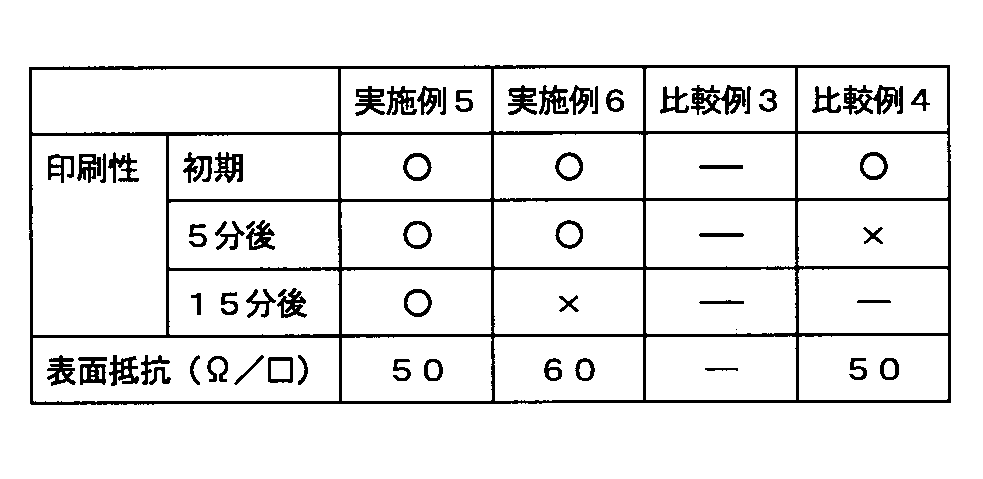
また、本発明のホウ素拡散用塗布液を用いて得られた半導体は、いずれも高い表面抵抗値を有するものであった。
Claims (4)
- 下記一般式(1)で表される1,2-ジオール構造単位を有するポリビニルアルコール系樹脂(A)、不純物(B)、および水(C)を含有することを特徴とする不純物拡散用塗布液。

- 上記不純物(B)が、13族元素化合物および15族元素化合物の少なくとも一つである請求項1記載の不純物拡散用塗布液。
- アルコール類(D)を含有する請求項1または2記載の不純物拡散用塗布液。
- 界面活性剤(E)を含有する請求項1~3のいずれか一項に記載の不純物拡散用塗布液。
Priority Applications (4)
| Application Number | Priority Date | Filing Date | Title |
|---|---|---|---|
| CN2011800568283A CN103229276A (zh) | 2010-11-29 | 2011-11-29 | 杂质扩散用涂布液 |
| EP11845216.8A EP2648211A4 (en) | 2010-11-29 | 2011-11-29 | COATING LIQUID FOR DIFFUSION OF CONTAMINATION |
| KR1020137013250A KR20130141547A (ko) | 2010-11-29 | 2011-11-29 | 불순물 확산용 도포액 |
| US13/989,112 US20130249059A1 (en) | 2010-11-29 | 2011-11-29 | Coating liquid for impurity diffusion |
Applications Claiming Priority (6)
| Application Number | Priority Date | Filing Date | Title |
|---|---|---|---|
| JP2010265349 | 2010-11-29 | ||
| JP2010-265349 | 2010-11-29 | ||
| JP2010-273662 | 2010-12-08 | ||
| JP2010273579 | 2010-12-08 | ||
| JP2010273662 | 2010-12-08 | ||
| JP2010-273579 | 2010-12-08 |
Publications (1)
| Publication Number | Publication Date |
|---|---|
| WO2012073920A1 true WO2012073920A1 (ja) | 2012-06-07 |
Family
ID=46171850
Family Applications (1)
| Application Number | Title | Priority Date | Filing Date |
|---|---|---|---|
| PCT/JP2011/077454 WO2012073920A1 (ja) | 2010-11-29 | 2011-11-29 | 不純物拡散用塗布液 |
Country Status (6)
| Country | Link |
|---|---|
| US (1) | US20130249059A1 (ja) |
| EP (1) | EP2648211A4 (ja) |
| KR (1) | KR20130141547A (ja) |
| CN (1) | CN103229276A (ja) |
| TW (1) | TWI494390B (ja) |
| WO (1) | WO2012073920A1 (ja) |
Cited By (2)
| Publication number | Priority date | Publication date | Assignee | Title |
|---|---|---|---|---|
| WO2012161107A1 (ja) * | 2011-05-20 | 2012-11-29 | 日本合成化学工業株式会社 | 不純物拡散用塗布液 |
| WO2013002236A1 (ja) * | 2011-06-28 | 2013-01-03 | 日本酢ビ・ポバール株式会社 | リン拡散用塗布液 |
Families Citing this family (10)
| Publication number | Priority date | Publication date | Assignee | Title |
|---|---|---|---|---|
| CN104981893B (zh) * | 2013-02-06 | 2018-01-30 | 松下生产工程技术株式会社 | 太阳能电池单元的制造方法 |
| WO2015056356A1 (en) * | 2013-10-17 | 2015-04-23 | The Nippon Synthetic Chemical Industry Co., Ltd. | Crosslinkable polymer |
| EP3137206B1 (en) | 2014-04-29 | 2019-11-27 | Basf Se | Process for producing microcapsules |
| US10307723B2 (en) | 2014-11-07 | 2019-06-04 | Basf Se | Process for preparing microcapsules having a polyurea shell and a lipophilic core material |
| EP3215103B1 (en) | 2014-11-07 | 2020-08-19 | Basf Se | Microcapsules comprising hydroxyalkyl cellulose |
| JP6883514B2 (ja) | 2014-11-07 | 2021-06-09 | ジボダン エス エー | カプセル組成物 |
| KR102547708B1 (ko) | 2014-11-07 | 2023-06-23 | 지보당 에스아 | 유기 화합물의 개선 또는 유기 화합물과 관련한 개선 |
| WO2017085033A1 (en) | 2015-11-18 | 2017-05-26 | Basf Se | Improvements in or relating to organic compounds |
| EP3170552A1 (en) | 2015-11-23 | 2017-05-24 | Basf Se | Microcapsule comprising a polymeric shell and a hydrophilic or hydrophobic core material |
| CN115148848A (zh) * | 2022-06-27 | 2022-10-04 | 常州时创能源股份有限公司 | 链式吸杂用磷源及其制备方法和应用 |
Citations (8)
| Publication number | Priority date | Publication date | Assignee | Title |
|---|---|---|---|---|
| US2518440A (en) * | 1948-08-09 | 1950-08-15 | Du Pont | Hydroxy-containing polymers |
| US5623086A (en) | 1995-12-29 | 1997-04-22 | Eastman Chemical Company | Process for the production of 1,2-bis (acyloxylates) |
| US6072079A (en) | 1999-03-03 | 2000-06-06 | Eastman Chemical Company | Continuous process for the production of diacetoxybutene |
| JP2000313721A (ja) * | 1999-03-01 | 2000-11-14 | Nippon Shokubai Co Ltd | 新規ヒドロキシル基含有共重合体とその製造方法 |
| JP2002284818A (ja) * | 2000-12-15 | 2002-10-03 | Nippon Synthetic Chem Ind Co Ltd:The | 新規ビニルアルコール系樹脂及びその用途 |
| JP2006095825A (ja) | 2004-09-29 | 2006-04-13 | Nippon Synthetic Chem Ind Co Ltd:The | 記録用媒体 |
| JP2007035719A (ja) | 2005-07-22 | 2007-02-08 | Nippon Synthetic Chem Ind Co Ltd:The | ホウ素拡散用塗布液 |
| JP2007053353A (ja) | 2005-07-22 | 2007-03-01 | Nippon Synthetic Chem Ind Co Ltd:The | リン拡散用塗布液 |
Family Cites Families (4)
| Publication number | Priority date | Publication date | Assignee | Title |
|---|---|---|---|---|
| ATE518925T1 (de) * | 2007-03-22 | 2011-08-15 | Nippon Synthetic Chem Ind | Wässrige zusammensetzung für ein aufzeichnungsmedium und tintenstrahlaufzeichnungsmedium damit |
| JP5748388B2 (ja) * | 2008-09-01 | 2015-07-15 | 日本酢ビ・ポバール株式会社 | ホウ素拡散用塗布液 |
| JP2010062334A (ja) * | 2008-09-03 | 2010-03-18 | Japan Vam & Poval Co Ltd | リン拡散用塗布液 |
| JP2010161317A (ja) * | 2009-01-09 | 2010-07-22 | Tokyo Ohka Kogyo Co Ltd | 拡散剤組成物、不純物拡散層の形成方法、および太陽電池 |
-
2011
- 2011-11-29 EP EP11845216.8A patent/EP2648211A4/en not_active Withdrawn
- 2011-11-29 CN CN2011800568283A patent/CN103229276A/zh active Pending
- 2011-11-29 WO PCT/JP2011/077454 patent/WO2012073920A1/ja active Application Filing
- 2011-11-29 TW TW100143812A patent/TWI494390B/zh not_active IP Right Cessation
- 2011-11-29 US US13/989,112 patent/US20130249059A1/en not_active Abandoned
- 2011-11-29 KR KR1020137013250A patent/KR20130141547A/ko not_active Application Discontinuation
Patent Citations (8)
| Publication number | Priority date | Publication date | Assignee | Title |
|---|---|---|---|---|
| US2518440A (en) * | 1948-08-09 | 1950-08-15 | Du Pont | Hydroxy-containing polymers |
| US5623086A (en) | 1995-12-29 | 1997-04-22 | Eastman Chemical Company | Process for the production of 1,2-bis (acyloxylates) |
| JP2000313721A (ja) * | 1999-03-01 | 2000-11-14 | Nippon Shokubai Co Ltd | 新規ヒドロキシル基含有共重合体とその製造方法 |
| US6072079A (en) | 1999-03-03 | 2000-06-06 | Eastman Chemical Company | Continuous process for the production of diacetoxybutene |
| JP2002284818A (ja) * | 2000-12-15 | 2002-10-03 | Nippon Synthetic Chem Ind Co Ltd:The | 新規ビニルアルコール系樹脂及びその用途 |
| JP2006095825A (ja) | 2004-09-29 | 2006-04-13 | Nippon Synthetic Chem Ind Co Ltd:The | 記録用媒体 |
| JP2007035719A (ja) | 2005-07-22 | 2007-02-08 | Nippon Synthetic Chem Ind Co Ltd:The | ホウ素拡散用塗布液 |
| JP2007053353A (ja) | 2005-07-22 | 2007-03-01 | Nippon Synthetic Chem Ind Co Ltd:The | リン拡散用塗布液 |
Non-Patent Citations (1)
| Title |
|---|
| See also references of EP2648211A4 * |
Cited By (2)
| Publication number | Priority date | Publication date | Assignee | Title |
|---|---|---|---|---|
| WO2012161107A1 (ja) * | 2011-05-20 | 2012-11-29 | 日本合成化学工業株式会社 | 不純物拡散用塗布液 |
| WO2013002236A1 (ja) * | 2011-06-28 | 2013-01-03 | 日本酢ビ・ポバール株式会社 | リン拡散用塗布液 |
Also Published As
| Publication number | Publication date |
|---|---|
| EP2648211A1 (en) | 2013-10-09 |
| EP2648211A4 (en) | 2014-07-30 |
| US20130249059A1 (en) | 2013-09-26 |
| KR20130141547A (ko) | 2013-12-26 |
| CN103229276A (zh) | 2013-07-31 |
| TW201231577A (en) | 2012-08-01 |
| TWI494390B (zh) | 2015-08-01 |
Similar Documents
| Publication | Publication Date | Title |
|---|---|---|
| WO2012073920A1 (ja) | 不純物拡散用塗布液 | |
| JP5748388B2 (ja) | ホウ素拡散用塗布液 | |
| JP4541243B2 (ja) | ホウ素拡散用塗布液 | |
| JP6000044B2 (ja) | 水性塗工液、および塗膜 | |
| JP4541328B2 (ja) | リン拡散用塗布液 | |
| JP5679545B2 (ja) | 拡散剤組成物、不純物拡散層の形成方法、および太陽電池 | |
| WO2014007263A1 (ja) | ドーパント拡散用塗布液、およびその塗布方法、並びにそれを用いた半導体の製法、半導体 | |
| WO2012161107A1 (ja) | 不純物拡散用塗布液 | |
| JP2010062334A (ja) | リン拡散用塗布液 | |
| JP2012138568A (ja) | 不純物拡散用塗布液 | |
| WO2013022076A1 (ja) | 太陽電池の製法およびそれにより得られた太陽電池 | |
| JP2013070048A (ja) | 太陽電池の製法およびそれにより得られた太陽電池 | |
| JP2012138569A (ja) | 不純物拡散用塗布液 | |
| JP5567163B2 (ja) | 拡散防止層形成用塗布液およびそれを用いたドーパント拡散層付き半導体基板の製法、並びに太陽電池の製法 | |
| JP2014099466A (ja) | ドーパント拡散用塗布液 | |
| JP2016134558A (ja) | ドーパント拡散用塗布液、およびそれを用いた半導体の製造方法 | |
| JP5731885B2 (ja) | ホウ素拡散用塗布液 | |
| JP6009245B2 (ja) | P型拡散層用塗布液 | |
| JP2013070047A (ja) | 太陽電池の製法およびそれにより得られた太陽電池 | |
| JP2013038411A (ja) | 半導体の製造方法 | |
| JP5241619B2 (ja) | アルカリ性水溶液組成物、およびそれを含有する表面処理用塗工液 | |
| JP2013070049A (ja) | 太陽電池の製法およびそれにより得られた太陽電池 | |
| JP6178543B2 (ja) | P型拡散層用塗布液 | |
| JP2015060870A (ja) | ドーパント拡散用塗布液、およびその塗布方法、並びにそれを用いた半導体の製法 | |
| JP2016115744A (ja) | ドーパント拡散用塗布液、およびそれを用いた半導体の製造方法 |
Legal Events
| Date | Code | Title | Description |
|---|---|---|---|
| 121 | Ep: the epo has been informed by wipo that ep was designated in this application |
Ref document number: 11845216 Country of ref document: EP Kind code of ref document: A1 |
|
| WWE | Wipo information: entry into national phase |
Ref document number: 13989112 Country of ref document: US |
|
| ENP | Entry into the national phase |
Ref document number: 20137013250 Country of ref document: KR Kind code of ref document: A |
|
| REEP | Request for entry into the european phase |
Ref document number: 2011845216 Country of ref document: EP |
|
| NENP | Non-entry into the national phase |
Ref country code: DE |