WO2012073773A1 - 基板および液晶表示装置 - Google Patents
基板および液晶表示装置 Download PDFInfo
- Publication number
- WO2012073773A1 WO2012073773A1 PCT/JP2011/076992 JP2011076992W WO2012073773A1 WO 2012073773 A1 WO2012073773 A1 WO 2012073773A1 JP 2011076992 W JP2011076992 W JP 2011076992W WO 2012073773 A1 WO2012073773 A1 WO 2012073773A1
- Authority
- WO
- WIPO (PCT)
- Prior art keywords
- substrate
- film material
- thin film
- liquid crystal
- alignment film
- Prior art date
- Legal status (The legal status is an assumption and is not a legal conclusion. Google has not performed a legal analysis and makes no representation as to the accuracy of the status listed.)
- Ceased
Links
Images









Classifications
-
- G—PHYSICS
- G02—OPTICS
- G02F—OPTICAL DEVICES OR ARRANGEMENTS FOR THE CONTROL OF LIGHT BY MODIFICATION OF THE OPTICAL PROPERTIES OF THE MEDIA OF THE ELEMENTS INVOLVED THEREIN; NON-LINEAR OPTICS; FREQUENCY-CHANGING OF LIGHT; OPTICAL LOGIC ELEMENTS; OPTICAL ANALOGUE/DIGITAL CONVERTERS
- G02F1/00—Devices or arrangements for the control of the intensity, colour, phase, polarisation or direction of light arriving from an independent light source, e.g. switching, gating or modulating; Non-linear optics
- G02F1/01—Devices or arrangements for the control of the intensity, colour, phase, polarisation or direction of light arriving from an independent light source, e.g. switching, gating or modulating; Non-linear optics for the control of the intensity, phase, polarisation or colour
- G02F1/13—Devices or arrangements for the control of the intensity, colour, phase, polarisation or direction of light arriving from an independent light source, e.g. switching, gating or modulating; Non-linear optics for the control of the intensity, phase, polarisation or colour based on liquid crystals, e.g. single liquid crystal display cells
- G02F1/133—Constructional arrangements; Operation of liquid crystal cells; Circuit arrangements
- G02F1/1333—Constructional arrangements; Manufacturing methods
- G02F1/1337—Surface-induced orientation of the liquid crystal molecules, e.g. by alignment layers
-
- G—PHYSICS
- G02—OPTICS
- G02F—OPTICAL DEVICES OR ARRANGEMENTS FOR THE CONTROL OF LIGHT BY MODIFICATION OF THE OPTICAL PROPERTIES OF THE MEDIA OF THE ELEMENTS INVOLVED THEREIN; NON-LINEAR OPTICS; FREQUENCY-CHANGING OF LIGHT; OPTICAL LOGIC ELEMENTS; OPTICAL ANALOGUE/DIGITAL CONVERTERS
- G02F1/00—Devices or arrangements for the control of the intensity, colour, phase, polarisation or direction of light arriving from an independent light source, e.g. switching, gating or modulating; Non-linear optics
- G02F1/01—Devices or arrangements for the control of the intensity, colour, phase, polarisation or direction of light arriving from an independent light source, e.g. switching, gating or modulating; Non-linear optics for the control of the intensity, phase, polarisation or colour
- G02F1/13—Devices or arrangements for the control of the intensity, colour, phase, polarisation or direction of light arriving from an independent light source, e.g. switching, gating or modulating; Non-linear optics for the control of the intensity, phase, polarisation or colour based on liquid crystals, e.g. single liquid crystal display cells
- G02F1/133—Constructional arrangements; Operation of liquid crystal cells; Circuit arrangements
- G02F1/1333—Constructional arrangements; Manufacturing methods
-
- G—PHYSICS
- G02—OPTICS
- G02F—OPTICAL DEVICES OR ARRANGEMENTS FOR THE CONTROL OF LIGHT BY MODIFICATION OF THE OPTICAL PROPERTIES OF THE MEDIA OF THE ELEMENTS INVOLVED THEREIN; NON-LINEAR OPTICS; FREQUENCY-CHANGING OF LIGHT; OPTICAL LOGIC ELEMENTS; OPTICAL ANALOGUE/DIGITAL CONVERTERS
- G02F1/00—Devices or arrangements for the control of the intensity, colour, phase, polarisation or direction of light arriving from an independent light source, e.g. switching, gating or modulating; Non-linear optics
- G02F1/01—Devices or arrangements for the control of the intensity, colour, phase, polarisation or direction of light arriving from an independent light source, e.g. switching, gating or modulating; Non-linear optics for the control of the intensity, phase, polarisation or colour
- G02F1/13—Devices or arrangements for the control of the intensity, colour, phase, polarisation or direction of light arriving from an independent light source, e.g. switching, gating or modulating; Non-linear optics for the control of the intensity, phase, polarisation or colour based on liquid crystals, e.g. single liquid crystal display cells
- G02F1/133—Constructional arrangements; Operation of liquid crystal cells; Circuit arrangements
- G02F1/1333—Constructional arrangements; Manufacturing methods
- G02F1/133354—Arrangements for aligning or assembling substrates
-
- G—PHYSICS
- G02—OPTICS
- G02F—OPTICAL DEVICES OR ARRANGEMENTS FOR THE CONTROL OF LIGHT BY MODIFICATION OF THE OPTICAL PROPERTIES OF THE MEDIA OF THE ELEMENTS INVOLVED THEREIN; NON-LINEAR OPTICS; FREQUENCY-CHANGING OF LIGHT; OPTICAL LOGIC ELEMENTS; OPTICAL ANALOGUE/DIGITAL CONVERTERS
- G02F1/00—Devices or arrangements for the control of the intensity, colour, phase, polarisation or direction of light arriving from an independent light source, e.g. switching, gating or modulating; Non-linear optics
- G02F1/01—Devices or arrangements for the control of the intensity, colour, phase, polarisation or direction of light arriving from an independent light source, e.g. switching, gating or modulating; Non-linear optics for the control of the intensity, phase, polarisation or colour
- G02F1/13—Devices or arrangements for the control of the intensity, colour, phase, polarisation or direction of light arriving from an independent light source, e.g. switching, gating or modulating; Non-linear optics for the control of the intensity, phase, polarisation or colour based on liquid crystals, e.g. single liquid crystal display cells
- G02F1/133—Constructional arrangements; Operation of liquid crystal cells; Circuit arrangements
- G02F1/1333—Constructional arrangements; Manufacturing methods
- G02F1/133388—Constructional arrangements; Manufacturing methods with constructional differences between the display region and the peripheral region
-
- Y—GENERAL TAGGING OF NEW TECHNOLOGICAL DEVELOPMENTS; GENERAL TAGGING OF CROSS-SECTIONAL TECHNOLOGIES SPANNING OVER SEVERAL SECTIONS OF THE IPC; TECHNICAL SUBJECTS COVERED BY FORMER USPC CROSS-REFERENCE ART COLLECTIONS [XRACs] AND DIGESTS
- Y10—TECHNICAL SUBJECTS COVERED BY FORMER USPC
- Y10T—TECHNICAL SUBJECTS COVERED BY FORMER US CLASSIFICATION
- Y10T428/00—Stock material or miscellaneous articles
- Y10T428/24—Structurally defined web or sheet [e.g., overall dimension, etc.]
- Y10T428/24479—Structurally defined web or sheet [e.g., overall dimension, etc.] including variation in thickness
Definitions
- the present invention relates to a substrate and a liquid crystal display device, and more particularly to a substrate on which a thin film is formed and a liquid crystal display device using the substrate.
- the liquid crystal display device generally has a structure in which a liquid crystal layer is sealed between a pair of substrates.
- One of the pair of substrates is a TFT substrate on which a plurality of gate wirings, a plurality of source wirings, a plurality of pixel electrodes, a plurality of TFTs (Thin-Film Transistors), and the like are formed.
- the other of the pair of substrates is a counter substrate in which a common electrode common to a plurality of pixel electrodes is formed.
- the liquid crystal layer is sealed between a TFT substrate and a counter substrate, surrounded by a frame-shaped sealing member.
- a pixel region as a display region and a frame region as a non-display region provided around the outside thereof are formed.
- the frame region of the TFT substrate has a seal member forming region and a terminal region provided on the outer periphery thereof.
- a plurality of terminals for supplying signals to the pixel area are formed.
- the TFT substrate and the counter substrate are provided with an alignment film for regulating the alignment of liquid crystal molecules in the liquid crystal layer on the surface on the liquid crystal layer side.
- the alignment film is made of, for example, a resin film such as polyimide, and its surface is subjected to a rubbing process or a photo-alignment process to add alignment performance.
- the alignment film is formed by applying liquid polyimide on the surface of the TFT substrate and the counter substrate, and then baking and curing.
- Polyimide can be applied by, for example, an ink jet printing method.
- a conventional technique for ejecting alignment film droplets onto a substrate using an inkjet printing method is disclosed in, for example, Japanese Patent Application Laid-Open No. 2006-320839 (Patent Document 1).
- the alignment film forming process using the inkjet method it is necessary to relatively reduce the viscosity of the alignment film material so that the alignment film material such as polyimide discharged and landed toward the substrate is sufficiently spread on the substrate surface. is there. Since the low-viscosity alignment film material easily spreads on the substrate surface, it easily spreads to a frame region that is not originally required.
- the liquid crystal display device there is a demand for a narrow frame that reduces the frame area around the outside of the display area.
- it is necessary to reduce the interval between the seal member arranged in the frame area and the pixel area.
- the low-viscosity alignment film material described above flows to the frame region and reaches the formation region of the seal member, an overlap between the seal member and the alignment film material occurs.
- the seal member and the alignment film material overlap, the adhesion between the seal member and the substrate decreases, and the outside air enters the liquid crystal layer from the interface between the seal member and the substrate. Therefore, it is important to apply the alignment film material to the substrate with high accuracy to prevent the seal member and the alignment film material from overlapping.
- the present invention has been made in view of the above-described problems, and a main object thereof is to provide a substrate that can improve the accuracy of arrangement of a thin film material supplied on the substrate surface on the substrate surface. Another object of the present invention is to provide a liquid crystal display device using the substrate.
- a substrate according to the present invention is a substrate having a surface and having a thin film formed on the surface, and provided with a plurality of island-shaped concave portions or convex portions formed on the surface in a two-dimensional array.
- a marking supplied with a thin film material for forming a thin film is formed at a part of the uneven shape including the uneven shape.
- the concavo-convex shape is formed by recessing a part of the surface.
- the concavo-convex shape is formed by projecting a part of the surface.
- the substrate has a thin film formation region on which a thin film is printed, and the position specifying portion is disposed outside the thin film formation region.
- the concave / convex shape is set with a coordinate system representing the positions of a plurality of island-shaped concave portions or convex portions.
- the liquid crystal display device includes a pair of substrates disposed opposite to each other and a liquid crystal layer disposed between the pair of substrates.
- the substrate includes a display area for displaying an image and a frame area around the outside of the display area.
- An alignment film obtained by curing a fluid alignment film material is formed on the surface of the substrate on the liquid crystal layer side.
- a concavo-convex shape in which a plurality of island-shaped concave portions or convex portions are two-dimensionally arranged is formed on at least one surface of the pair of substrates.
- a marking supplied with an alignment film material for forming an alignment film is formed at a part of the uneven shape.
- the substrate of the present invention it is possible to improve the placement accuracy of the supplied thin film material on the substrate surface.
- FIG. 1 is a cross-sectional view illustrating a schematic configuration of a liquid crystal display device according to a first embodiment. It is a top view of the liquid crystal display device shown in FIG. It is sectional drawing which expands and shows a part of TFT substrate. It is a top view which expands and shows a part of TFT substrate. It is sectional drawing which expands and shows the support structure part in a TFT substrate. It is a top view which expands and shows a part of counter substrate.
- FIG. 7 is a cross-sectional view of a part of the counter substrate along the line VII-VII shown in FIG. 6. It is a schematic diagram of the mother glass in which a TFT substrate is formed. It is an enlarged view of the area
- FIG. 10 is a cross-sectional view of the alignment mark along the line XX shown in FIG. 9.
- FIG. 11 is a schematic diagram showing a state in which a thin film material droplet is dropped on the alignment mark shown in FIGS. It is a schematic diagram which shows the thin film material adhering to the alignment mark. It is a schematic diagram of the mother glass in which a counter substrate is formed. It is an enlarged view of the area
- FIG. 15 is a cross-sectional view of the alignment mark along the line XV-XV shown in FIG.
- FIG. 16 is a schematic diagram showing a state in which a thin film material droplet is dropped on the alignment mark shown in FIGS.
- FIG. 6 is a cross-sectional view illustrating a schematic configuration of a liquid crystal display device according to a second embodiment.
- FIG. 1 is a cross-sectional view showing a schematic configuration of the liquid crystal display device 1 of the first embodiment.
- FIG. 2 is a plan view of the liquid crystal display device 1 shown in FIG.
- FIG. 1 is a cross-sectional view of the liquid crystal display device 1 taken along line II in FIG.
- the liquid crystal display device 1 includes a TFT substrate 11 as a first substrate, a counter substrate 12 that is a second substrate disposed to face the TFT substrate 11, a TFT substrate 11, And a liquid crystal layer 13 provided between the counter substrates 12.
- the pair of TFT substrates 11 and the counter substrate 12 are disposed to face each other.
- the liquid crystal layer 13 is disposed between the pair of TFT substrates 11 and the counter substrate 12.
- the liquid crystal display device 1 also includes a seal member 14 provided between the TFT substrate 11 and the counter substrate 12. As shown in FIG. 2, the seal member 14 is formed in a substantially rectangular frame shape and surrounds and seals the liquid crystal layer 13.
- the seal member 14 is made of, for example, an ultraviolet heat combined curable resin such as acrylic or epoxy resin.
- a plurality of spacers and conductive particles (not shown) are dispersed and mixed in the seal member 14.
- the line width of the seal member 14 is, for example, about 0.5 mm to 2.5 mm.
- the TFT substrate 11 and the counter substrate 12 each include a pixel region 31 as a display region for displaying an image and a frame region 32 as a non-display region that is an outer peripheral region of the pixel region 31.
- the frame region 32 includes a seal member formation region 34 (a formation region of the seal member 14) provided at a predetermined interval from the pixel region 31.
- a plurality of lead wires 17 are formed in the frame region 32.
- the line width of the lead-out wiring 17 is about 10 ⁇ m.
- An interval between adjacent lead-out wirings 17 is about 20 ⁇ m in the seal member forming region 34.
- the frame region 32 of the TFT substrate 11 has a terminal region 33 which is a region opposite to the pixel region 31 with respect to the seal member forming region 34.
- the terminal region 33 is formed in a side region of the TFT substrate 11 as shown in FIG.
- a plurality of terminals 28 for supplying signals to the pixel region 31 are formed in the terminal region 33.
- a pad 20 is formed as a laminated electrode portion made of a conductive film and a transparent conductive film such as ITO (Indium Tin Oxide).
- a plurality of pads 20 are formed on the surface of the planarizing film 43 shown in FIG.
- the pad 20 is formed of ITO having a thickness of about 100 nm so as to make a through hole in the lower insulating layer and tangent to the lower wiring, and is arranged along the seal member 14 at a predetermined interval.
- the pad 20 is for electrically connecting to the common electrode 26 of the counter substrate 12 through the conductive particles of the seal member 14.
- a plurality of pixels 5 are arranged in a matrix in the pixel region 31 of the TFT substrate 11.
- Each pixel 5 is formed with a pixel electrode 15 made of a transparent conductive film such as ITO.
- Each pixel 5 is formed with a TFT (not shown) as a switching element connected to the pixel electrode 15. Further, the TFT substrate 11 is formed with gate wiring and source wiring (not shown) connected to the TFT.
- the TFT substrate 11 has a glass substrate 21 as a support substrate, and a surface 21a on the liquid crystal layer 13 side of the glass substrate 21 is a gate that covers the gate wiring (not shown).
- An insulating film 41 is formed.
- the gate insulating film 41 is made of an oxide film such as SiN or SiO 2 and has a thickness of about 0.4 ⁇ m.
- the plurality of lead lines 17 are made of the same material as the gate lines, and terminals 28 are provided at the ends of the lead lines 17.
- the source wiring is connected to the lead wiring 17.
- a passivation film 42 as a protective film is formed on the surface of the gate insulating film 41.
- the passivation film 42 is made of an inorganic film such as SiN, and has a thickness of about 0.25 ⁇ m.
- a planarizing film 43 which is an insulating film that covers the passivation film 42, is formed.
- the planarizing film 43 is made of, for example, a photocurable acrylic resin and has a thickness of about 2.5 ⁇ m.
- the plurality of pixel electrodes 15 are formed on the surface of the planarizing film 43 in the pixel region 31.
- the sealing member 14 is formed on the surface of the planarizing film 43 in the sealing member forming region 34.
- a support structure 50 that supports the alignment film 23 and the alignment film material 24 is constituted by a part of the planarizing film 43.
- an alignment film 23 formed by curing a fluid alignment film material 24 is formed so as to spread from the pixel region 31 to the formation region side of the seal member 14. Yes.
- the surface 11a (see FIG. 1) of the TFT substrate 11 on the liquid crystal layer 13 side is directly covered with the alignment film 23.
- the alignment film 23 is made of a resin material such as polyimide and regulates the initial alignment of the liquid crystal molecules of the liquid crystal layer 13.
- the alignment film material 24 has its viscosity lowered by adding a solvent to polyimide or the like.
- a vertical alignment film material having a viscosity of 6.5 mPa ⁇ s manufactured by JSR Corporation can be applied.
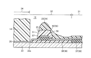
- FIG. 5 is an enlarged cross-sectional view showing the support structure portion 50 in the TFT substrate 11.
- the side portion 51 of the support structure 50 has a tangential plane 53 in contact with the surface of the side portion 51 toward the glass substrate 21 side. It is formed so as to incline toward a certain seal member forming region 34 side.
- the side portion 51 of the support structure 50 is disposed between the pixel region 31 and the plurality of terminals 28 (particularly, between the pixel region 31 and the seal member forming region 34 in the present embodiment) and oriented.
- the edge 23 of the film 23 and the alignment film material 24 is supported.
- the angle formed between the tangential plane 53 of the side 51 and the surface of the glass substrate 21 at the edge 25 of the alignment film 23 and the alignment film material 24 is ⁇ 1
- the angle at the edge 25 of the alignment film 23 and the like is
- An angle formed between the tangential plane 54 on the surface of the edge 25 and the tangential plane 53 is defined as ⁇ 2.
- the alignment film material 24 flowing from the pixel region 31 side can be blocked by the angle ⁇ 2 in the side portion 51.
- the alignment film 23 and the alignment film material 24 swell toward the liquid crystal layer 13 in the vicinity of the side portion 51 of the support structure portion 50.
- FIG. 6 is an enlarged plan view showing a part of the counter substrate 12.
- FIG. 7 is a cross-sectional view of a part of the counter substrate 12 taken along the line VII-VII shown in FIG.
- the counter substrate 12 has a glass substrate 22 that is a support substrate.
- a plurality of colored layers 37 constituting a color filter 36 and a black matrix 38 as a light shielding film are formed on the surface 22a of the glass substrate 22 on the liquid crystal layer 13 side.
- the thickness of the black matrix 38 is about 1.5 ⁇ m.
- a common electrode 26 made of a transparent conductive film such as ITO is also formed on the surface 22a with a thickness of about 100 nm.
- the colored layer 37 is a filter that transmits R (red), G (green), or B (blue) light, and is arranged in a matrix in the pixel region 31 of the counter substrate 12.
- the black matrix 38 is formed to shield between the adjacent colored layers 37 and to shield the frame region 32 from light.
- the seal member 14 is the same as that formed on the TFT substrate 11 and is disposed in the seal member forming region 34 of the frame region 32.
- An alignment film 23 formed by curing the same alignment film material 24 formed on the TFT substrate 11 also spreads from the pixel region 31 to the seal member formation region 34 side on the liquid crystal layer 13 side of the counter substrate 12. Is formed. A surface 12 a (see FIG. 1) on the liquid crystal layer 13 side of the counter substrate 12 is directly covered with the alignment film 23.
- the support structure 50 is formed on the counter substrate 12 as well as the TFT substrate 11.
- the support structure part 50 is provided in the vicinity of the seal member forming region 34, and is configured by a ridge 56 extending in a rib shape along the seal member 14.
- the protrusion 56 has a base part 57 made of the same material as that of the blue colored layer 37, for example, and a covering part 58 that covers the base part 57.
- the covering portion 58 is made of a photosensitive acrylic resin that is the same material as ribs (not shown) or photo spacers (not shown) for controlling the vertical alignment of liquid crystal molecules formed on the counter substrate 12.
- the support structure portion 50 of the counter substrate 12 also has side portions 51 similar to the support structure portion 50 of the TFT substrate 11.
- the side portion 51 of the support structure portion 50 in the counter substrate 12 is also disposed between the pixel region 31 and the seal member forming region 34.
- the edge portions 25 of the alignment film 23 and the alignment film material 24 are similarly supported by the side portions 51.
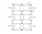
- FIG. 8 is a schematic diagram of the mother glass 60 on which the TFT substrate 11 is formed.
- a plurality of glass substrates 21 are generally formed by cutting a large glass plate called a mother glass 60.
- FIG. 8 shows an example in which six TFT substrates 11 are formed from one mother glass 60.
- a region corresponding to the glass substrate 21 in the mother glass 60 is specified as the thin film formation region 62.
- the mother glass 60 functions as an inkjet printing substrate on which a thin film is printed on the surface 61 (see FIG. 10 described later) by the inkjet method.
- By forming thin films typified by the gate insulating film 41, the passivation film 42, the planarizing film 43, the alignment film 23, and the like in the thin film forming region 62, a plurality of TFT substrates 11 are manufactured.
- the thin film formation region 62 has a rectangular planar shape.
- An alignment mark 70 is disposed outside the thin film formation region 62 near the vertex of the rectangle.
- the alignment mark 70 is a position where a droplet of a thin film material forming the thin film (for example, a droplet 24a of the alignment film material 24 forming the alignment film 23 shown in FIG. 11) is dropped onto the surface 61 of the mother glass 60. It functions as a position specifying unit for specifying.
- FIG. 9 is an enlarged view of the region IX shown in FIG.
- FIG. 10 is a cross-sectional view of the alignment mark 70 along the line XX shown in FIG.
- the alignment mark 70 includes an uneven shape 72 formed by processing a part of the surface 61 of the mother glass 60. More specifically, the concavo-convex shape 72 is provided with a plurality of island-shaped concave portions 73 formed by recessing a part of the surface 61 in a two-dimensional array.
- the concave and convex shape 72 is formed by the plurality of concave portions 73 from which part of the surface 61 of the mother glass 60 is removed and the bowl-shaped portions 74 provided between the adjacent concave portions 73 and projecting relative to the concave portions 73.
- the island shape means that each of the plurality of recesses 73 is not connected and is provided discontinuously.
- a hook-shaped portion 74 is formed so as to surround the periphery of the recess 73.
- each of the recesses 73 is formed in a square shape in plan view.
- a plurality of recesses 73 are formed so as to be aligned along one direction (left-right direction in FIG. 9).
- a plurality of recesses 73 are linearly arranged so as to extend in the one direction.
- a group of recesses 73 arranged in a straight line are arranged in order in another direction (vertical direction in FIG. 9) orthogonal to the one direction. In this way, the alignment mark 70 having a shape spreading in a plane as shown in FIG. 9 is formed.
- the hook-shaped portion 74 extends linearly along the one direction over the entire alignment mark 70, and separates the group of concave portions 73 arranged in the other direction from each other. Moreover, the hook-shaped part 74 extended along the said other direction is formed and has a length corresponding to the length along the said other direction of the one recessed part 73, and is divided finely. Referring to FIG. 9, regarding the group of recesses 73 arranged in the other direction, the hook-like portions 74 along the other direction formed in the other group of recesses 73 are located at the same position in the one direction. Has been placed.
- the hook-shaped portion 74 formed between the recesses 73 in one row is formed between the recesses 73 in the other row in the one direction. It arrange
- the length of one side of the square formed by the recess 73 may be 100 ⁇ m.
- the line width of the bowl-shaped portion 74 is smaller than the length of one side of the concave portion 73, and may be 30 ⁇ m, for example.
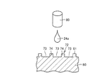
- FIG. 11 is a schematic view showing a state in which the thin film material droplet 24a is dropped on the alignment mark 70 shown in FIGS.
- FIG. 12 is a schematic diagram showing the thin film material attached to the alignment mark 70.
- the droplets 24a of the thin film material having fluidity filled in the coating device 80 are dropped at a position where the alignment mark 70 is formed on the surface 61 of the mother glass 60 as shown in FIG.
- FIG. 12 shows a state where the droplet 24a has landed inside the recess 73.
- FIG. Since the thin film material in the example shown in FIG. 12, the alignment film material 24) has low viscosity and high fluidity, as shown in FIG. 12, the alignment film material 24 partially protrudes from the recess 73 where the droplet 24 a has landed, It flows so as to ride on the upper side of the bowl-shaped portion 74.
- the alignment film material 24 tends to flow from the bowl-shaped portion 74 to the adjacent concave portion 73. However, as described with reference to FIG. 5, the alignment film material 24 is supported by the hook-shaped portion 74, so that the alignment film material 24 is blocked by the hook-shaped portion 74, and from the surface 61 of the mother glass 60. It gets excited.
- the recess 73 and the bowl-shaped portion 74 of the alignment mark 70 function as a blocking portion 71 that blocks the flow along the surface 61 of the droplet 24 a of the alignment film material 24 dropped on the surface 61 of the mother glass 60.
- the blocking portion 71 includes an uneven shape 72 formed on a part of the surface 61, thereby suppressing the thin film material from spreading along the surface 61.
- a marking 78 to which the alignment film material 24 for forming the alignment film 23 is supplied is formed at a part of the uneven shape 72 of the alignment mark 70.
- FIG. 13 is a schematic diagram of the mother glass 60 on which the counter substrate 12 is formed. Similar to the mother glass 60 on which the TFT substrate 11 is formed, the mother glass 60 on which the counter substrate 12 shown in FIG. 13 is formed has a thin film printed on the surface 61 (see FIG. 15 described later) by an inkjet method. Function as a substrate for inkjet printing. Six counter substrates 12 are formed from one mother glass 60, and a region corresponding to the glass substrate 22 in the mother glass 60 is specified as the thin film formation region 62.
- Alignment marks 70 are arranged outside the thin film formation region 62 in the vicinity of the apex of the thin film formation region 62 having a rectangular planar shape.
- the alignment mark 70 is a position where a droplet of a thin film material forming the thin film (for example, a droplet 24a of the alignment film material 24 forming the alignment film 23 shown in FIG. 16) is dropped on the surface 61 of the mother glass 60. It functions as a position specifying unit for specifying.
- FIG. 14 is an enlarged view of region XIV shown in FIG.
- FIG. 15 is a cross-sectional view of the alignment mark 70 along the line XV-XV shown in FIG.
- the alignment mark 70 includes an uneven shape 72 formed by processing a part of the surface 61 of the mother glass 60. More specifically, the concavo-convex shape 72 is provided with a plurality of island-shaped convex portions 75 formed by projecting a part of the surface 61 in a two-dimensional array. An uneven shape is formed by a plurality of convex portions 75 that are raised on the surface 61 side of the mother glass 60 and a groove-like portion 76 that is provided between adjacent convex portions 75 and that is recessed relative to the convex portions 75. 72 is formed. As a result of the convex portion 75 being formed in an island shape, a groove-like portion 76 is formed so as to surround the periphery of the convex portion 75.
- the alignment mark 70 formed on the counter substrate 12 has concavities and convexities reversed as compared with the alignment mark 70 of the TFT substrate 11 described above.
- the alignment mark 70 of the counter substrate 12 shown in FIG. 14 has the same planar shape as the alignment mark 70 of the TFT substrate 11 described with reference to FIG.
- Each of the convex portions 75 is formed in a square shape in plan view.
- the length of one side of the square formed by the convex portions 75 may be 100 ⁇ m.
- the line width of the groove-like portion 76 is smaller than the length of one side of the convex portion 75, and may be 30 ⁇ m, for example.
- FIG. 16 is a schematic diagram showing a state in which a thin film material droplet 24a is dropped on the alignment mark 70 shown in FIGS.
- FIG. 17 is a schematic diagram showing the thin film material attached to the alignment mark 70. Liquid droplets 24a of fluid thin film material filled in the coating device 80 are dropped onto the surface 61 of the mother glass 60 where the alignment marks 70 are formed as shown in FIG. FIG. 17 shows a state where the droplet 24a has landed on the upper surface of the convex portion 75.
- FIG. 16 is a schematic diagram showing a state in which a thin film material droplet 24a is dropped on the alignment mark 70 shown in FIGS.
- FIG. 17 is a schematic diagram showing the thin film material attached to the alignment mark 70. Liquid droplets 24a of fluid thin film material filled in the coating device 80 are dropped onto the surface 61 of the mother glass 60 where the alignment marks 70 are formed as shown in FIG.
- FIG. 17 shows a state where the droplet 24a has landed on the upper surface of the conve
- the periphery of the convex portion 75 is framed from the convex portion 75 where the droplet 24a has landed. It tends to flow toward the groove-shaped portion 76 that surrounds the shape.
- the alignment film material 24 is blocked by the alignment film material 24 being supported by the side portions of the convex portions 75.
- the convex portion 75 and the groove-like portion 76 of the alignment mark 70 function as a blocking portion 71 that blocks the flow along the surface 61 of the droplet 24 a of the alignment film material 24 dropped on the surface 61 of the mother glass 60.
- the blocking portion 71 includes an uneven shape 72 formed on a part of the surface 61, thereby suppressing the thin film material from spreading along the surface 61. As a result, a marking 78 to which the alignment film material 24 for forming the alignment film 23 is supplied is formed at a part of the uneven shape 72 of the alignment mark 70.
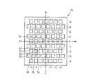
- FIG. 18 is a schematic diagram showing a target position 91 where the droplet 24a is dropped on the alignment mark 70 and a landing position 92 of the droplet 24a.
- an alignment mark 70 formed on the counter substrate 12 is shown as an example.
- the intersection of the X axis and the Y axis, which are two orthogonal axes shown in FIG. 18, indicates the center position of the target for landing the droplet 24 a of the alignment film material 24, and this position is referred to as a target position 91.
- the position where the droplet 24 a is actually dropped on the surface 61 of the mother glass 60 is referred to as a landing position 92.
- a coordinate system representing the positions of the plurality of island-shaped convex portions 75 is set in the uneven shape 72 of the alignment mark 70.
- the coordinates of the target position 91 are (0, 0), and the coordinates of the landing position 92 are ( ⁇ 2, ⁇ 2).
- This coordinate system can be formed of the black matrix 38 in the case of the counter substrate 12.
- the coordinate system can be formed by a gate wiring, a source wiring, or a silicon layer.
- the landing position 92 is shifted in both the X-axis direction and the Y-axis direction with respect to the target position 91 where the thin film material is to be dropped.
- the alignment system 70 With the coordinate system shown in FIG. 18, it can be immediately confirmed whether or not the landing position 92 is deviated from the target position 91.
- the thin film material can be accurately applied to the substrate surface by inkjet. In this way, a thin film such as the alignment film 23 can be formed more accurately in a planar manner.
- the seal member 14 and the alignment film material 24 do not overlap even if the interval between the seal member 14 and the pixel region 31 is narrowed.
- the alignment film material 24 can be applied to the glass substrates 21 and 22 with high accuracy. Therefore, a narrow frame of the liquid crystal display device 1 can be achieved.
- the alignment mark 70 for grasping the deviation between the target position 91 and the landing position 92 of the alignment film material 24 is disposed outside the thin film formation region 62, the alignment mark 70 is formed when the liquid crystal display device 1 is formed. This will not interfere with the installation of the terminal or wiring.
- a corner portion forming an angle of 90 ° is formed at the apex of the rectangular thin film formation region 62, and an alignment mark 70 is formed on a 45 ° line that bisects the 90 ° angle.
- a structure in which the alignment mark 70 is formed symmetrically is desirable because the thin film material can be applied with higher accuracy.
- liquid crystal display device 1 a frame-shaped seal member 14 is formed on the TFT substrate 11 or the counter substrate 12, and after the liquid crystal is dropped inside the seal member 14, the TFT substrate 11 and the counter substrate 12 are bonded to each other. Manufactured by. After the two mother glasses 60 and 60 shown in FIGS. 8 and 13 are bonded together with the positions of the respective thin film formation regions 62 aligned, the laminated body of the mother glasses 60 is individually cut to obtain a liquid crystal display device. 1 is produced.
- a gate wiring (not shown), a gate insulating film 41, a silicon film (not shown), a source wiring 16, a passivation film 42, A planarizing film 43 is formed. Thereafter, a plurality of recesses 48 are formed through the planarizing film 43, the passivation film 42 and the gate insulating film 41 by photolithography and etching. Inside the recess 48, the glass substrate 21 is exposed when there is no metal layer on the base. Thus, the support structure portion 50 is formed as a part of the planarizing film 43.
- the recess 73 is formed. Thereby, the alignment mark 70 which can control the expansion range of the alignment film material 24 is formed. Since the concave portion 73 can be formed at the same time as the concave portion 48 is formed, an additional process for forming the concave portion 73 is not necessary, and a reduction in productivity of the TFT substrate 11 can be prevented.
- an ITO layer is formed on the surface of the planarizing film 43, and a plurality of pixel electrodes 15 are formed by patterning the ITO layer by photolithography and etching.
- the target position 91 is set in the alignment mark 70, and the droplet 24 a of the alignment film material 24 is transferred to the alignment mark 70 with the target position 91 as the target dropping position. Dripping.
- the landing position 92 where the dropped liquid droplet 24a actually landed is detected, the positional deviation between the target position 91 and the landing position 92 is calculated, and the positional deviation is reduced (typically, the positional deviation amount is reduced to zero).
- the setting of the coating device 80 for the alignment film material 24 is changed. Thereafter, a fluid alignment film material 24 such as polyimide is supplied by an ink jet method so as to cover the pixel electrode 15 and the like.
- the alignment film material 24 flows from the pixel region 31 to the frame region 32, and when the alignment film material 24 reaches the side 51 of the support structure 50, the edge 25 of the alignment film material 24 is supported by the side 51. . As a result, as shown in FIG. 3, the alignment film material 24 rises toward the liquid crystal layer 13 and is dammed in the vicinity of the side portion 51 of the support structure portion 50. Thereafter, the alignment film material 24 is baked to form the alignment film 23.
- the common electrode 26 and the color filter 36 are formed on the surface of the glass substrate 22 which is a transparent substrate.
- the base portion 57 is formed of the same material as the colored layer 37 on the surface of the black matrix 38 in the frame region 32.
- the convex portion 75 is formed.
- the alignment mark 70 which can control the expansion range of the alignment film material 24 is formed. Since the convex portions 75 can be formed simultaneously with the formation of the colored layer 37, an additional step for forming the convex portions 75 is not necessary, and a decrease in productivity of the counter substrate 12 can be prevented.
- a photo-sensitive acrylic resin is deposited so as to cover the base portion 57 and the color filter 36, and then this is subjected to photolithography and development, thereby covering the base portion 57 and a photo spacer. (Not shown) or ribs for controlling the vertical alignment of liquid crystal molecules are formed simultaneously.
- the target position 91 is set in the alignment mark 70, and the droplet 24 a of the alignment film material 24 is transferred to the alignment mark 70 with the target position 91 as the target dropping position. Dripping.
- the landing position 92 where the dropped liquid droplet 24a actually landed is detected, the positional deviation between the target position 91 and the landing position 92 is calculated, and the positional deviation is reduced (typically, the positional deviation amount is reduced to zero).
- the setting of the coating device 80 for the alignment film material 24 is changed. Thereafter, a fluid alignment film material 24 such as polyimide is supplied by an ink jet method so as to cover the color filter 36 and the like.
- the alignment film material 24 flows from the pixel region 31 to the frame region 32, and when the alignment film material 24 reaches the side 51 of the support structure 50, the edge 25 of the alignment film material 24 is supported by the side 51. . As a result, as shown in FIG. 7, the alignment film material 24 rises toward the liquid crystal layer 13 and is dammed in the vicinity of the side portion 51 of the support structure portion 50. Thereafter, the alignment film material 24 is baked to form the alignment film 23.
- the droplet 24a of the alignment film material 24 is dropped on the alignment mark 70 before the inkjet coating of the alignment film material 24 having high fluidity, and the positional deviation between the target position 91 and the landing position 92 is adjusted.
- the alignment film material 24 can be applied by inkjet with high accuracy.
- the alignment film 23 can be arranged with high accuracy in a plane, so that the alignment with the seal member 14 is possible. Overlap with the film material 24 can be prevented, and the adhesion of the seal member 14 can be ensured.
- the alignment mark 70 formed on the mother glass 60 on the TFT substrate 11 side is formed by forming a gate wiring, a silicon layer or a source wiring, or creating a contact hole of a photosensitive acrylic resin that is an interlayer insulating film. May be.
- the alignment mark 70 formed on the mother glass 60 on the counter substrate 12 side may be formed by using a colored layer such as a black matrix, a liquid crystal alignment control rib, or a photo spacer.
- FIG. 19 is a cross-sectional view illustrating a schematic configuration of the liquid crystal display device according to the second embodiment.
- the liquid crystal display device of the second embodiment has the same configuration as the liquid crystal display device 1 of the first embodiment described above.
- an alignment mark 70 as a position specifying part for specifying the dropping position of the droplet 24a of the alignment film material 24 is formed in the frame region 32 of the TFT substrate 11 and the counter substrate 12, and the alignment is performed.
- the mark 70 is different from the first embodiment in that the mark 70 has a blocking portion 71 that blocks the flow along the surface of the droplet 24 a dropped on the surface 11 a of the TFT substrate 11 and the surface 12 a of the counter substrate 12.
- the alignment mark 70 is formed outside the thin film formation region 62 of the mother glass 60, and the alignment mark 70 does not appear on the liquid crystal display device 1 that is a product.
- the liquid crystal display device according to the second embodiment includes an alignment mark 70 in the frame region 32 of the TFT substrate 11 and the counter substrate 12 as shown in FIG. Even with such a configuration, as in the first embodiment, the arrangement accuracy of the alignment film material 24 to be applied by inkjet can be improved. Since the alignment mark 70 is formed at a position closer to the pixel region 31 where the alignment film 23 is formed, the arrangement accuracy of the alignment film 23 can be further improved.
- the alignment mark 70 is formed on both the TFT substrate 11 and the counter substrate 12. However, the alignment mark 70 is formed on either the TFT substrate 11 or the counter substrate 12. Also good.
- the alignment film material 24 is applied to the TFT substrate 11 and the counter substrate 12 of the liquid crystal display device 1 by inkjet.
- the present invention is limited to this application. It is not something that can be done.
- the thin film material with high accuracy can be obtained by applying the alignment mark 70 described in the first and second embodiments. Ink jet coating is possible.
- the present invention is not limited to the liquid crystal display device 1 and can be applied to any application in which a thin film material having high fluidity that spreads more than the accuracy required after dropping ink hits the substrate surface is applied by ink jetting.
- the present invention can be applied to resist film coating of a semiconductor device.
- SYMBOLS 1 Liquid crystal display device, 11 TFT substrate, 11a, 12a surface, 12 Opposing substrate, 14 Seal member, 21, 22 Glass substrate, 23 Alignment film, 24 Alignment film material, 24a droplet, 31 pixel area, 32 frame area, 60 Mother glass, 61 surface, 62 thin film formation area, 70 alignment mark, 71 blocking part, 72 uneven shape, 73 recessed part, 74 saddle-shaped part, 75 convex part, 76 grooved part, 80 coating device, 91 target position, 92 landing position.
Landscapes
- Physics & Mathematics (AREA)
- Nonlinear Science (AREA)
- Mathematical Physics (AREA)
- Chemical & Material Sciences (AREA)
- Crystallography & Structural Chemistry (AREA)
- General Physics & Mathematics (AREA)
- Optics & Photonics (AREA)
- Liquid Crystal (AREA)
- Spectroscopy & Molecular Physics (AREA)
Abstract
Description
上記基板において好ましくは、凹凸形状は、表面の一部を突起させて形成されている。
図1は、実施の形態1の液晶表示装置1の概略構成を示す断面図である。図2は、図1に示す液晶表示装置1の平面図である。なお図1は、図2中に示すI-I線に沿う液晶表示装置1の断面図である。図1および図2に示すように、液晶表示装置1は、第1基板としてのTFT基板11と、TFT基板11に対向して配置された第2基板である対向基板12と、TFT基板11および対向基板12の間に設けられた液晶層13とを備える。一対のTFT基板11と対向基板12とは、互いに対向して配置されている。液晶層13は、一対のTFT基板11と対向基板12との間に配置されている。
図19は、実施の形態2の液晶表示装置の概略構成を示す断面図である。実施の形態2の液晶表示装置は、上述した実施の形態1の液晶表示装置1と同様の構成を備えている。しかし、実施の形態2では、TFT基板11と対向基板12との額縁領域32に配向膜材料24の液滴24aの滴下位置を特定する位置特定部としてのアライメントマーク70が形成されており、アライメントマーク70はTFT基板11の表面11aおよび対向基板12の表面12aに滴下された液滴24aの表面に沿う流れを遮る遮断部71を有する点で、実施の形態1とは異なっている。
Claims (6)
- 表面(61)を有し、前記表面(61)上に薄膜(23)が形成される基板(60)であって、
前記表面(61)に形成された複数の島状の凹部(73)または凸部(75)が二次元的に配列されて設けられた凹凸形状(72)を含み、
前記凹凸形状(72)の一部箇所には、前記薄膜(23)を形成する薄膜材料(24)が供給されたマーキング(78)が形成されている、基板(60)。 - 前記凹凸形状(72)は、前記表面(61)の一部を窪ませて形成されている、請求項1に記載の基板(60)。
- 前記凹凸形状(72)は、前記表面(61)の一部を突起させて形成されている、請求項1に記載の基板(60)。
- 前記表面(61)上に前記薄膜(23)が形成される薄膜形成領域(62)を有し、
前記凹凸形状(72)は、前記薄膜形成領域(62)の外側に配置されている、請求項1から請求項3のいずれかに記載の基板(60)。 - 前記凹凸形状(72)には、複数の島状の前記凹部(73)または前記凸部(75)の位置を表す座標系が設定されている、請求項1から請求項4のいずれかに記載の基板(60)。
- 互いに対向して配置された一対の基板(11,12)と、
前記一対の基板(11,12)の間に配置された液晶層(13)と、を備え、
前記基板(11,12)は、画像を表示する表示領域(31)と、前記表示領域(31)の外側周囲の額縁領域(32)と、を含み、
前記基板(11,12)の前記液晶層(13)側の表面(11a,12a)には、流動性を有する配向膜材料(24)が硬化された配向膜(23)が形成されており、
前記一対の基板(11,12)の少なくともいずれか一方の前記表面(11a,12a)には、複数の島状の凹部(73)または凸部(75)が二次元的に配列されて設けられた凹凸形状(72)が形成されており、
前記凹凸形状(72)の一部箇所には、前記配向膜(23)を形成する前記配向膜材料(24)が供給されたマーキング(78)が形成されている、液晶表示装置(1)。
Priority Applications (3)
| Application Number | Priority Date | Filing Date | Title |
|---|---|---|---|
| CN201180057753.0A CN103238104B (zh) | 2010-11-30 | 2011-11-24 | 基板和液晶显示装置 |
| JP2012546802A JP5490922B2 (ja) | 2010-11-30 | 2011-11-24 | 基板および液晶表示装置 |
| US13/883,317 US20130235314A1 (en) | 2010-11-30 | 2011-11-24 | Substrate and liquid crystal display device |
Applications Claiming Priority (2)
| Application Number | Priority Date | Filing Date | Title |
|---|---|---|---|
| JP2010267243 | 2010-11-30 | ||
| JP2010-267243 | 2010-11-30 |
Publications (1)
| Publication Number | Publication Date |
|---|---|
| WO2012073773A1 true WO2012073773A1 (ja) | 2012-06-07 |
Family
ID=46171715
Family Applications (1)
| Application Number | Title | Priority Date | Filing Date |
|---|---|---|---|
| PCT/JP2011/076992 Ceased WO2012073773A1 (ja) | 2010-11-30 | 2011-11-24 | 基板および液晶表示装置 |
Country Status (4)
| Country | Link |
|---|---|
| US (1) | US20130235314A1 (ja) |
| JP (1) | JP5490922B2 (ja) |
| CN (1) | CN103238104B (ja) |
| WO (1) | WO2012073773A1 (ja) |
Families Citing this family (14)
| Publication number | Priority date | Publication date | Assignee | Title |
|---|---|---|---|---|
| CN204389840U (zh) * | 2015-01-04 | 2015-06-10 | 京东方科技集团股份有限公司 | 一种基板及光电显示装置 |
| CN104570450A (zh) * | 2015-02-05 | 2015-04-29 | 京东方科技集团股份有限公司 | 一种显示基板、显示面板和显示装置 |
| KR20160123424A (ko) * | 2015-04-15 | 2016-10-26 | 삼성디스플레이 주식회사 | 액정 표시 장치 |
| CN105093697B (zh) * | 2015-08-21 | 2018-03-30 | 深圳市华星光电技术有限公司 | 基板及确定基板配向膜边界的位置的方法 |
| JP2017067874A (ja) * | 2015-09-28 | 2017-04-06 | 株式会社ジャパンディスプレイ | 表示装置およびその製造方法 |
| CN105511144A (zh) * | 2016-01-27 | 2016-04-20 | 京东方科技集团股份有限公司 | 一种显示基板、显示面板和显示装置 |
| CN105572939A (zh) * | 2016-02-01 | 2016-05-11 | 武汉华星光电技术有限公司 | 液晶显示面板的对位组立方法 |
| CN107329295A (zh) * | 2017-08-25 | 2017-11-07 | 深圳市华星光电技术有限公司 | 一种聚酰亚胺薄膜位置测量方法及对位标记 |
| CN108445678A (zh) * | 2018-05-04 | 2018-08-24 | 张家港康得新光电材料有限公司 | 一种转印版 |
| CN109143629B (zh) * | 2018-09-28 | 2022-05-20 | 张家港康得新光电材料有限公司 | 一种显示面板母版中配向膜位置精度的检测方法 |
| CN111367104A (zh) * | 2018-12-25 | 2020-07-03 | 上海摩软通讯技术有限公司 | Lcd显示玻璃及其加工方法、移动终端 |
| US11551777B2 (en) * | 2019-08-09 | 2023-01-10 | Micron Technology, Inc. | Apparatus with circuit-locating mechanism |
| CN111596486B (zh) * | 2020-06-22 | 2023-06-30 | 成都京东方显示科技有限公司 | 基板及其制作方法、显示面板 |
| CN114296270A (zh) * | 2022-02-23 | 2022-04-08 | 滁州惠科光电科技有限公司 | 彩膜基板制备方法、彩膜基板及显示面板 |
Citations (3)
| Publication number | Priority date | Publication date | Assignee | Title |
|---|---|---|---|---|
| JPH08273997A (ja) * | 1995-03-29 | 1996-10-18 | Oki Electric Ind Co Ltd | アライメントマーク |
| JP2004212490A (ja) * | 2002-12-27 | 2004-07-29 | Casio Comput Co Ltd | 液晶素子 |
| JP2006234975A (ja) * | 2005-02-22 | 2006-09-07 | Seiko Epson Corp | 位置合わせ用パターン、表示デバイス、表示デバイスの組立て方法、表示デバイスの位置合わせ検査方法 |
Family Cites Families (11)
| Publication number | Priority date | Publication date | Assignee | Title |
|---|---|---|---|---|
| US5702567A (en) * | 1995-06-01 | 1997-12-30 | Kabushiki Kaisha Toshiba | Plurality of photolithographic alignment marks with shape, size and spacing based on circuit pattern features |
| JP3507274B2 (ja) * | 1997-03-31 | 2004-03-15 | 三洋電機株式会社 | マザーガラス基板およびその製造方法 |
| JPH11142844A (ja) * | 1997-11-07 | 1999-05-28 | Canon Inc | 液晶表示装置 |
| WO2000019497A1 (en) * | 1998-09-30 | 2000-04-06 | Nikon Corporation | Alignment method and method for producing device using the alignment method |
| JP2006320839A (ja) * | 2005-05-19 | 2006-11-30 | Sharp Corp | 配向膜の液滴吐出方法及び液滴吐出装置 |
| JP2006335422A (ja) * | 2005-06-02 | 2006-12-14 | Key Tranding Co Ltd | 模様付容器の製法およびそれによって得られる模様付容器 |
| JP2007003651A (ja) * | 2005-06-22 | 2007-01-11 | Nec Lcd Technologies Ltd | 液晶表示パネル及びその製造方法 |
| JP4768393B2 (ja) * | 2005-10-21 | 2011-09-07 | Nec液晶テクノロジー株式会社 | 液晶表示装置およびその製造方法 |
| JP2009047827A (ja) * | 2007-08-17 | 2009-03-05 | Seiko Epson Corp | カラーフィルタ基板の製造方法、及びカラーフィルタ基板 |
| JP2009092733A (ja) * | 2007-10-04 | 2009-04-30 | Seiko Epson Corp | カラーフィルタ基板の製造方法 |
| JP2009298041A (ja) * | 2008-06-13 | 2009-12-24 | Toshiba Corp | テンプレート及びパターン形成方法 |
-
2011
- 2011-11-24 CN CN201180057753.0A patent/CN103238104B/zh not_active Expired - Fee Related
- 2011-11-24 US US13/883,317 patent/US20130235314A1/en not_active Abandoned
- 2011-11-24 JP JP2012546802A patent/JP5490922B2/ja not_active Expired - Fee Related
- 2011-11-24 WO PCT/JP2011/076992 patent/WO2012073773A1/ja not_active Ceased
Patent Citations (3)
| Publication number | Priority date | Publication date | Assignee | Title |
|---|---|---|---|---|
| JPH08273997A (ja) * | 1995-03-29 | 1996-10-18 | Oki Electric Ind Co Ltd | アライメントマーク |
| JP2004212490A (ja) * | 2002-12-27 | 2004-07-29 | Casio Comput Co Ltd | 液晶素子 |
| JP2006234975A (ja) * | 2005-02-22 | 2006-09-07 | Seiko Epson Corp | 位置合わせ用パターン、表示デバイス、表示デバイスの組立て方法、表示デバイスの位置合わせ検査方法 |
Also Published As
| Publication number | Publication date |
|---|---|
| JP5490922B2 (ja) | 2014-05-14 |
| CN103238104B (zh) | 2015-08-19 |
| JPWO2012073773A1 (ja) | 2014-05-19 |
| CN103238104A (zh) | 2013-08-07 |
| US20130235314A1 (en) | 2013-09-12 |
Similar Documents
| Publication | Publication Date | Title |
|---|---|---|
| JP5490922B2 (ja) | 基板および液晶表示装置 | |
| US11061288B2 (en) | Liquid crystal display device | |
| JP5302460B2 (ja) | 液晶表示装置及びその製造方法 | |
| JP5593332B2 (ja) | 液晶表示装置及びその製造方法 | |
| KR101647882B1 (ko) | 표시장치 및 표시장치의 제조방법 | |
| TWI519873B (zh) | Liquid crystal display device and manufacturing method thereof | |
| CN101794050A (zh) | 彩色电泳显示装置及其制造方法 | |
| KR20090060159A (ko) | 액정 표시 소자 및 액정 표시 소자의 제조 방법 | |
| JP5379245B2 (ja) | 液晶表示装置 | |
| JP2006071750A (ja) | 液晶表示装置 | |
| US11022846B2 (en) | Substrate for display device and display device | |
| WO2008044364A1 (en) | Liquid crystal display | |
| US9170459B2 (en) | Liquid crystal display device and manufacturing method thereof | |
| JP6616897B2 (ja) | 表示パネル | |
| JP2011053552A (ja) | 液晶表示装置 | |
| KR20120070072A (ko) | 액정 표시 장치 및 그 제조 방법 | |
| KR102263995B1 (ko) | 액정표시패널용 기판, 그 제조 방법, 이를 포함하는 액정표시패널 | |
| KR20110100741A (ko) | 표시패널 및 그 제조방법 | |
| WO2018173857A1 (ja) | 表示パネル | |
| JP2007187961A (ja) | 液晶表示装置の製造方法 | |
| JP2009063622A (ja) | 液晶表示装置およびその製造方法 | |
| WO2018221315A1 (ja) | 表示パネル及び連成表示パネル | |
| JP2008096574A (ja) | 液晶表示素子 | |
| JP2006235057A (ja) | 液晶表示素子 | |
| JP2010197508A (ja) | 画像表示装置 |
Legal Events
| Date | Code | Title | Description |
|---|---|---|---|
| 121 | Ep: the epo has been informed by wipo that ep was designated in this application |
Ref document number: 11844832 Country of ref document: EP Kind code of ref document: A1 |
|
| WWE | Wipo information: entry into national phase |
Ref document number: 13883317 Country of ref document: US |
|
| ENP | Entry into the national phase |
Ref document number: 2012546802 Country of ref document: JP Kind code of ref document: A |
|
| NENP | Non-entry into the national phase |
Ref country code: DE |
|
| 122 | Ep: pct application non-entry in european phase |
Ref document number: 11844832 Country of ref document: EP Kind code of ref document: A1 |