WO2012060299A1 - Iii族窒化物半導体素子、iii族窒化物半導体素子を作製する方法、及びエピタキシャル基板 - Google Patents
Iii族窒化物半導体素子、iii族窒化物半導体素子を作製する方法、及びエピタキシャル基板 Download PDFInfo
- Publication number
- WO2012060299A1 WO2012060299A1 PCT/JP2011/074973 JP2011074973W WO2012060299A1 WO 2012060299 A1 WO2012060299 A1 WO 2012060299A1 JP 2011074973 W JP2011074973 W JP 2011074973W WO 2012060299 A1 WO2012060299 A1 WO 2012060299A1
- Authority
- WO
- WIPO (PCT)
- Prior art keywords
- group iii
- gallium nitride
- nitride semiconductor
- semiconductor layer
- iii nitride
- Prior art date
- Legal status (The legal status is an assumption and is not a legal conclusion. Google has not performed a legal analysis and makes no representation as to the accuracy of the status listed.)
- Ceased
Links
Images


Classifications
-
- H—ELECTRICITY
- H01—ELECTRIC ELEMENTS
- H01S—DEVICES USING THE PROCESS OF LIGHT AMPLIFICATION BY STIMULATED EMISSION OF RADIATION [LASER] TO AMPLIFY OR GENERATE LIGHT; DEVICES USING STIMULATED EMISSION OF ELECTROMAGNETIC RADIATION IN WAVE RANGES OTHER THAN OPTICAL
- H01S5/00—Semiconductor lasers
- H01S5/30—Structure or shape of the active region; Materials used for the active region
- H01S5/34—Structure or shape of the active region; Materials used for the active region comprising quantum well or superlattice structures, e.g. single quantum well [SQW] lasers, multiple quantum well [MQW] lasers or graded index separate confinement heterostructure [GRINSCH] lasers
- H01S5/343—Structure or shape of the active region; Materials used for the active region comprising quantum well or superlattice structures, e.g. single quantum well [SQW] lasers, multiple quantum well [MQW] lasers or graded index separate confinement heterostructure [GRINSCH] lasers in AIIIBV compounds, e.g. AlGaAs-laser, InP-based laser
- H01S5/34333—Structure or shape of the active region; Materials used for the active region comprising quantum well or superlattice structures, e.g. single quantum well [SQW] lasers, multiple quantum well [MQW] lasers or graded index separate confinement heterostructure [GRINSCH] lasers in AIIIBV compounds, e.g. AlGaAs-laser, InP-based laser with a well layer based on Ga(In)N or Ga(In)P, e.g. blue laser
-
- B—PERFORMING OPERATIONS; TRANSPORTING
- B82—NANOTECHNOLOGY
- B82Y—SPECIFIC USES OR APPLICATIONS OF NANOSTRUCTURES; MEASUREMENT OR ANALYSIS OF NANOSTRUCTURES; MANUFACTURE OR TREATMENT OF NANOSTRUCTURES
- B82Y20/00—Nanooptics, e.g. quantum optics or photonic crystals
-
- H—ELECTRICITY
- H01—ELECTRIC ELEMENTS
- H01L—SEMICONDUCTOR DEVICES NOT COVERED BY CLASS H10
- H01L21/00—Processes or apparatus adapted for the manufacture or treatment of semiconductor or solid state devices or of parts thereof
- H01L21/02—Manufacture or treatment of semiconductor devices or of parts thereof
- H01L21/02104—Forming layers
- H01L21/02365—Forming inorganic semiconducting materials on a substrate
- H01L21/02367—Substrates
- H01L21/0237—Materials
- H01L21/02387—Group 13/15 materials
- H01L21/02389—Nitrides
-
- H—ELECTRICITY
- H01—ELECTRIC ELEMENTS
- H01L—SEMICONDUCTOR DEVICES NOT COVERED BY CLASS H10
- H01L21/00—Processes or apparatus adapted for the manufacture or treatment of semiconductor or solid state devices or of parts thereof
- H01L21/02—Manufacture or treatment of semiconductor devices or of parts thereof
- H01L21/02104—Forming layers
- H01L21/02365—Forming inorganic semiconducting materials on a substrate
- H01L21/02436—Intermediate layers between substrates and deposited layers
- H01L21/02439—Materials
- H01L21/02455—Group 13/15 materials
- H01L21/02458—Nitrides
-
- H—ELECTRICITY
- H01—ELECTRIC ELEMENTS
- H01L—SEMICONDUCTOR DEVICES NOT COVERED BY CLASS H10
- H01L21/00—Processes or apparatus adapted for the manufacture or treatment of semiconductor or solid state devices or of parts thereof
- H01L21/02—Manufacture or treatment of semiconductor devices or of parts thereof
- H01L21/02104—Forming layers
- H01L21/02365—Forming inorganic semiconducting materials on a substrate
- H01L21/02436—Intermediate layers between substrates and deposited layers
- H01L21/02494—Structure
- H01L21/02496—Layer structure
- H01L21/02505—Layer structure consisting of more than two layers
-
- H—ELECTRICITY
- H01—ELECTRIC ELEMENTS
- H01L—SEMICONDUCTOR DEVICES NOT COVERED BY CLASS H10
- H01L21/00—Processes or apparatus adapted for the manufacture or treatment of semiconductor or solid state devices or of parts thereof
- H01L21/02—Manufacture or treatment of semiconductor devices or of parts thereof
- H01L21/02104—Forming layers
- H01L21/02365—Forming inorganic semiconducting materials on a substrate
- H01L21/02518—Deposited layers
- H01L21/02521—Materials
- H01L21/02538—Group 13/15 materials
- H01L21/0254—Nitrides
-
- H—ELECTRICITY
- H01—ELECTRIC ELEMENTS
- H01L—SEMICONDUCTOR DEVICES NOT COVERED BY CLASS H10
- H01L21/00—Processes or apparatus adapted for the manufacture or treatment of semiconductor or solid state devices or of parts thereof
- H01L21/02—Manufacture or treatment of semiconductor devices or of parts thereof
- H01L21/02104—Forming layers
- H01L21/02365—Forming inorganic semiconducting materials on a substrate
- H01L21/02518—Deposited layers
- H01L21/0257—Doping during depositing
- H01L21/02573—Conductivity type
- H01L21/02579—P-type
-
- H—ELECTRICITY
- H01—ELECTRIC ELEMENTS
- H01L—SEMICONDUCTOR DEVICES NOT COVERED BY CLASS H10
- H01L21/00—Processes or apparatus adapted for the manufacture or treatment of semiconductor or solid state devices or of parts thereof
- H01L21/02—Manufacture or treatment of semiconductor devices or of parts thereof
- H01L21/02104—Forming layers
- H01L21/02365—Forming inorganic semiconducting materials on a substrate
- H01L21/02612—Formation types
- H01L21/02617—Deposition types
- H01L21/0262—Reduction or decomposition of gaseous compounds, e.g. CVD
-
- H—ELECTRICITY
- H01—ELECTRIC ELEMENTS
- H01S—DEVICES USING THE PROCESS OF LIGHT AMPLIFICATION BY STIMULATED EMISSION OF RADIATION [LASER] TO AMPLIFY OR GENERATE LIGHT; DEVICES USING STIMULATED EMISSION OF ELECTROMAGNETIC RADIATION IN WAVE RANGES OTHER THAN OPTICAL
- H01S5/00—Semiconductor lasers
- H01S5/02—Structural details or components not essential to laser action
- H01S5/028—Coatings ; Treatment of the laser facets, e.g. etching, passivation layers or reflecting layers
-
- H—ELECTRICITY
- H10—SEMICONDUCTOR DEVICES; ELECTRIC SOLID-STATE DEVICES NOT OTHERWISE PROVIDED FOR
- H10H—INORGANIC LIGHT-EMITTING SEMICONDUCTOR DEVICES HAVING POTENTIAL BARRIERS
- H10H20/00—Individual inorganic light-emitting semiconductor devices having potential barriers, e.g. light-emitting diodes [LED]
- H10H20/80—Constructional details
- H10H20/81—Bodies
- H10H20/822—Materials of the light-emitting regions
- H10H20/824—Materials of the light-emitting regions comprising only Group III-V materials, e.g. GaP
- H10H20/825—Materials of the light-emitting regions comprising only Group III-V materials, e.g. GaP containing nitrogen, e.g. GaN
- H10H20/8252—Materials of the light-emitting regions comprising only Group III-V materials, e.g. GaP containing nitrogen, e.g. GaN characterised by the dopants
-
- H10P14/24—
-
- H10P14/2908—
-
- H10P14/3216—
-
- H10P14/3251—
-
- H10P14/3416—
-
- H10P14/3444—
-
- H—ELECTRICITY
- H01—ELECTRIC ELEMENTS
- H01S—DEVICES USING THE PROCESS OF LIGHT AMPLIFICATION BY STIMULATED EMISSION OF RADIATION [LASER] TO AMPLIFY OR GENERATE LIGHT; DEVICES USING STIMULATED EMISSION OF ELECTROMAGNETIC RADIATION IN WAVE RANGES OTHER THAN OPTICAL
- H01S2302/00—Amplification / lasing wavelength
-
- H—ELECTRICITY
- H01—ELECTRIC ELEMENTS
- H01S—DEVICES USING THE PROCESS OF LIGHT AMPLIFICATION BY STIMULATED EMISSION OF RADIATION [LASER] TO AMPLIFY OR GENERATE LIGHT; DEVICES USING STIMULATED EMISSION OF ELECTROMAGNETIC RADIATION IN WAVE RANGES OTHER THAN OPTICAL
- H01S2304/00—Special growth methods for semiconductor lasers
- H01S2304/04—MOCVD or MOVPE
-
- H—ELECTRICITY
- H01—ELECTRIC ELEMENTS
- H01S—DEVICES USING THE PROCESS OF LIGHT AMPLIFICATION BY STIMULATED EMISSION OF RADIATION [LASER] TO AMPLIFY OR GENERATE LIGHT; DEVICES USING STIMULATED EMISSION OF ELECTROMAGNETIC RADIATION IN WAVE RANGES OTHER THAN OPTICAL
- H01S5/00—Semiconductor lasers
- H01S5/20—Structure or shape of the semiconductor body to guide the optical wave ; Confining structures perpendicular to the optical axis, e.g. index or gain guiding, stripe geometry, broad area lasers, gain tailoring, transverse or lateral reflectors, special cladding structures, MQW barrier reflection layers
- H01S5/2004—Confining in the direction perpendicular to the layer structure
- H01S5/2009—Confining in the direction perpendicular to the layer structure by using electron barrier layers
-
- H—ELECTRICITY
- H01—ELECTRIC ELEMENTS
- H01S—DEVICES USING THE PROCESS OF LIGHT AMPLIFICATION BY STIMULATED EMISSION OF RADIATION [LASER] TO AMPLIFY OR GENERATE LIGHT; DEVICES USING STIMULATED EMISSION OF ELECTROMAGNETIC RADIATION IN WAVE RANGES OTHER THAN OPTICAL
- H01S5/00—Semiconductor lasers
- H01S5/20—Structure or shape of the semiconductor body to guide the optical wave ; Confining structures perpendicular to the optical axis, e.g. index or gain guiding, stripe geometry, broad area lasers, gain tailoring, transverse or lateral reflectors, special cladding structures, MQW barrier reflection layers
- H01S5/2004—Confining in the direction perpendicular to the layer structure
- H01S5/2018—Optical confinement, e.g. absorbing-, reflecting- or waveguide-layers
- H01S5/2031—Optical confinement, e.g. absorbing-, reflecting- or waveguide-layers characterized by special waveguide layers, e.g. asymmetric waveguide layers or defined bandgap discontinuities
-
- H—ELECTRICITY
- H01—ELECTRIC ELEMENTS
- H01S—DEVICES USING THE PROCESS OF LIGHT AMPLIFICATION BY STIMULATED EMISSION OF RADIATION [LASER] TO AMPLIFY OR GENERATE LIGHT; DEVICES USING STIMULATED EMISSION OF ELECTROMAGNETIC RADIATION IN WAVE RANGES OTHER THAN OPTICAL
- H01S5/00—Semiconductor lasers
- H01S5/30—Structure or shape of the active region; Materials used for the active region
- H01S5/305—Structure or shape of the active region; Materials used for the active region characterised by the doping materials used in the laser structure
- H01S5/3054—Structure or shape of the active region; Materials used for the active region characterised by the doping materials used in the laser structure p-doping
- H01S5/3063—Structure or shape of the active region; Materials used for the active region characterised by the doping materials used in the laser structure p-doping using Mg
-
- H—ELECTRICITY
- H01—ELECTRIC ELEMENTS
- H01S—DEVICES USING THE PROCESS OF LIGHT AMPLIFICATION BY STIMULATED EMISSION OF RADIATION [LASER] TO AMPLIFY OR GENERATE LIGHT; DEVICES USING STIMULATED EMISSION OF ELECTROMAGNETIC RADIATION IN WAVE RANGES OTHER THAN OPTICAL
- H01S5/00—Semiconductor lasers
- H01S5/30—Structure or shape of the active region; Materials used for the active region
- H01S5/32—Structure or shape of the active region; Materials used for the active region comprising PN junctions, e.g. hetero- or double- heterostructures
- H01S5/3202—Structure or shape of the active region; Materials used for the active region comprising PN junctions, e.g. hetero- or double- heterostructures grown on specifically orientated substrates, or using orientation dependent growth
- H01S5/320275—Structure or shape of the active region; Materials used for the active region comprising PN junctions, e.g. hetero- or double- heterostructures grown on specifically orientated substrates, or using orientation dependent growth semi-polar orientation
-
- H—ELECTRICITY
- H01—ELECTRIC ELEMENTS
- H01S—DEVICES USING THE PROCESS OF LIGHT AMPLIFICATION BY STIMULATED EMISSION OF RADIATION [LASER] TO AMPLIFY OR GENERATE LIGHT; DEVICES USING STIMULATED EMISSION OF ELECTROMAGNETIC RADIATION IN WAVE RANGES OTHER THAN OPTICAL
- H01S5/00—Semiconductor lasers
- H01S5/30—Structure or shape of the active region; Materials used for the active region
- H01S5/32—Structure or shape of the active region; Materials used for the active region comprising PN junctions, e.g. hetero- or double- heterostructures
- H01S5/3211—Structure or shape of the active region; Materials used for the active region comprising PN junctions, e.g. hetero- or double- heterostructures characterised by special cladding layers, e.g. details on band-discontinuities
- H01S5/3213—Structure or shape of the active region; Materials used for the active region comprising PN junctions, e.g. hetero- or double- heterostructures characterised by special cladding layers, e.g. details on band-discontinuities asymmetric clading layers
-
- H—ELECTRICITY
- H10—SEMICONDUCTOR DEVICES; ELECTRIC SOLID-STATE DEVICES NOT OTHERWISE PROVIDED FOR
- H10H—INORGANIC LIGHT-EMITTING SEMICONDUCTOR DEVICES HAVING POTENTIAL BARRIERS
- H10H20/00—Individual inorganic light-emitting semiconductor devices having potential barriers, e.g. light-emitting diodes [LED]
- H10H20/80—Constructional details
- H10H20/81—Bodies
- H10H20/811—Bodies having quantum effect structures or superlattices, e.g. tunnel junctions
- H10H20/812—Bodies having quantum effect structures or superlattices, e.g. tunnel junctions within the light-emitting regions, e.g. having quantum confinement structures
Definitions
- the present invention relates to a group III nitride semiconductor device, a method for manufacturing a group III nitride semiconductor device, and an epitaxial substrate.
- Patent Document 1 describes a method of growing an InGaN layer for a blue light emitting device. It defines the growth temperature and growth rate during InGaN growth.
- the carrier gas is switched to nitrogen at a substrate temperature of 805 degrees Celsius, and TMG, TMI, ammonia, and silane are allowed to flow to grow Si-doped InGaN.
- the only gas supplied from the conical quartz tube is nitrogen.
- Patent Document 1 hydrogen and nitrogen are allowed to flow for GaN growth on the c-plane, while nitrogen is allowed to flow for InGaN growth.
- a gallium nitride based semiconductor not containing In, for example, GaN or AlGaN is grown while supplying hydrogen.
- oxygen is desorbed from the residual material in the growth furnace, such as jigs and deposits. This oxygen is taken into the epitaxial film as a result in the epitaxial growth on the nonpolar surface where oxygen is easily taken in.
- a group III nitride semiconductor device includes: (a) a conductive substrate including a main surface made of a first gallium nitride semiconductor; and (b) a first p-type gallium nitride semiconductor.
- a group III nitride semiconductor region including a layer and provided on the main surface.
- the main surface of the substrate is inclined at an angle in a range of 50 degrees to less than 130 degrees from a plane orthogonal to a reference axis extending along the c-axis of the first gallium nitride semiconductor, and the first p-type
- the oxygen concentration of the gallium nitride based semiconductor layer is 5 ⁇ 10 17 cm ⁇ 3 or less, and the ratio of the p-type dopant concentration Npd of the first p-type gallium nitride based semiconductor layer to the oxygen concentration Noxg (Noxg / Npd) Is 1/10 or less.
- the first p-type gallium nitride semiconductor layer is provided on the main surface of the substrate, and the main surface extends along the c-axis of the first gallium nitride semiconductor of the substrate. It inclines at an angle in the range of 50 degrees or more and less than 130 degrees from a plane orthogonal to the extending reference axis.
- the oxygen concentration in the first p-type gallium nitride semiconductor layer can be 5 ⁇ 10 17 cm ⁇ 3 or less, so that oxygen contained in the first p-type gallium nitride semiconductor layer causes the first p-type gallium nitride semiconductor layer to Compensation of the p-type dopant in the p-type gallium nitride based semiconductor layer can be reduced. Moreover, since the ratio (Noxg / Npd) is 1/10 or less, the p-type dopant concentration Npd can be lowered.
- the first p-type gallium nitride based semiconductor layer preferably does not contain indium as a group III constituent element.
- the oxygen concentration can be reduced and the p-type dopant concentration Npd can be lowered.
- the group III nitride semiconductor device may further include an n-type gallium nitride semiconductor layer provided on the main surface and a gallium nitride semiconductor layer for the light emitting layer.
- the light emitting layer may be provided between the first p-type gallium nitride semiconductor layer and the n-type gallium nitride semiconductor layer, and the group III nitride semiconductor device may be a light emitting device. According to this group III nitride semiconductor device, the electrical characteristics of the p-type gallium nitride based semiconductor layer in the light emitting device can be improved.
- the emission wavelength of the light emitting layer may be not less than 440 nm and not more than 600 nm.
- the electrical characteristics of the p-type gallium nitride semiconductor can be improved in the light-emitting device that generates light in the above-described emission wavelength range.
- the emission wavelength of the light emitting layer may be not less than 490 nm and not more than 600 nm.
- the electrical characteristics of the p-type gallium nitride semiconductor can be improved in a light emitting device that provides light emission at a long wavelength.
- the group III nitride semiconductor device may further include an electrode in contact with the group III nitride semiconductor region.
- the group III nitride semiconductor region includes a contact layer in contact with the electrode and a p-type group III nitride semiconductor stack, and the p-type group III nitride semiconductor stack includes a contact layer and a light emitting layer.
- the p-type group III nitride semiconductor multilayer is formed between and in contact with the contact layer to form a first junction and the light emitting layer to form a second junction.
- the oxygen concentration is 5 ⁇ 10 17 cm ⁇ 3 or less, and the ratio (Noxg / Npd) between the p-type dopant concentration Npd and the oxygen concentration Noxg of the p-type group III nitride semiconductor stack is 1/10 or less. Is good.
- the oxygen concentration in the p-type group III nitride semiconductor stack is reduced and the ratio (Noxg / Npd) is reduced to 1/10 or less. Reduced.
- the electrical characteristics of the p-type group III nitride semiconductor constituting this current path can be improved.
- the first p-type gallium nitride based semiconductor layer can be made of GaN, InGaN, AlGaN, or InAlGaN.
- the oxygen concentration is reduced and the ratio (Noxg / Npd) is 1 / It is reduced to 10 or less.
- the first p-type gallium nitride based semiconductor layer can be made of GaN or AlGaN.
- the oxygen concentration is reduced and the ratio (Noxg / Npd) is reduced to 1/10 or less. Reduced.
- the first p-type gallium nitride based semiconductor layer may have a carbon concentration of 1 ⁇ 10 17 cm ⁇ 3 or less.
- this group III nitride semiconductor device it is required to lower the growth temperature of the p-layer semiconductor, particularly in the production of a light emitting device that emits light at a long wavelength, and therefore the concentration of carbon impurities increases.
- the concentration of carbon impurities increases.
- the first p-type gallium nitride based semiconductor layer grown in a nitrogen atmosphere not only the oxygen concentration but also the carbon concentration can be reduced.
- the group III nitride semiconductor region further includes a second p-type gallium nitride based semiconductor layer provided on the main surface.
- the oxygen concentration of the p-type gallium nitride based semiconductor layer is 5 ⁇ 10 17 cm ⁇ 3 or less
- the second p-type gallium nitride based semiconductor layer contains indium as a group III constituent element
- the second p-type gallium nitride based semiconductor layer The ratio (Noxg / Npd) between the p-type dopant concentration Npd of the gallium nitride based semiconductor layer and the oxygen concentration Noxg may be 1/10 or less.
- the oxygen concentration can be reduced and the concentration ratio (Noxg / Npd) can be reduced to 1/10 or less. it can. Therefore, the electrical characteristics of this p-type group III nitride semiconductor can be improved.
- Another aspect of the present invention is a method for fabricating a group III nitride semiconductor device.
- the method includes (a) preparing a conductive substrate including a main surface made of a first gallium nitride semiconductor, and (b) a group III nitride including a first p-type gallium nitride semiconductor layer. And a step of growing a semiconductor region on the main surface.
- a source gas and a first atmospheric gas for the group III constituent element and the group V constituent element of the first p-type gallium nitride semiconductor layer grow.
- Nitrogen is used as the first atmospheric gas supplied to the furnace, and the main surface of the substrate is at least 50 degrees from a surface orthogonal to a reference axis extending along the c-axis of the first gallium nitride semiconductor.
- the first p-type gallium nitride based semiconductor layer is inclined at an angle of less than 130 degrees, and the oxygen concentration of the first p-type gallium nitride based semiconductor layer is 5 ⁇ 10 17 cm ⁇ 3 or less.
- the ratio (Noxg / Npd) between the type dopant concentration Npd and the oxygen concentration Noxg is 1/10 or less.
- the first p-type gallium nitride semiconductor layer is grown on the main surface of the substrate, and the main surface extends along the c-axis of the first gallium nitride semiconductor of the substrate. It inclines at an angle in the range of 50 degrees or more and less than 130 degrees from a plane perpendicular to the angle.
- the source gas for the first p-type gallium nitride based semiconductor layer and the first atmospheric gas are supplied to the growth furnace, and nitrogen is used as the atmospheric gas. Therefore, the oxygen concentration in the first p-type gallium nitride based semiconductor layer can be set to 5 ⁇ 10 17 cm ⁇ 3 or less.
- Compensation of the p-type dopant in the first p-type gallium nitride semiconductor layer by oxygen contained in the first p-type gallium nitride semiconductor layer can be reduced. Further, since the concentration ratio (Noxg / Npd) is 1/10 or less, the p-type dopant concentration Npd can be lowered.
- the first p-type gallium nitride based semiconductor layer may not contain indium as a group III constituent element. According to this manufacturing method, in a gallium nitride semiconductor that does not contain indium as a group III constituent element, the oxygen concentration can be reduced and the concentration ratio can be lowered.
- the manufacturing method includes a step of growing an n-type gallium nitride semiconductor layer on the main surface, and a step of growing a gallium nitride semiconductor layer for an active layer on the main surface; Can be further provided.
- the active layer is provided between the p-type gallium nitride semiconductor layer and the n-type gallium nitride semiconductor layer, and the group III nitride semiconductor device is a light emitting device. According to this manufacturing method, the electrical characteristics of the p-type gallium nitride based semiconductor layer in the light emitting element can be improved.
- the emission wavelength of the active layer may be not less than 440 nm and not more than 600 nm. According to this manufacturing method, the electrical characteristics of the p-type gallium nitride semiconductor can be improved in the light-emitting element that generates light in the above-described emission wavelength range.
- the emission wavelength of the active layer may be not less than 490 nm and not more than 600 nm. According to this manufacturing method, the characteristics of the p-type gallium nitride semiconductor can be improved in a light-emitting element that provides light emission at a long wavelength.
- the manufacturing method according to another aspect of the present invention may further include a step of forming an electrode that is in contact with the group III nitride semiconductor region.
- the group III nitride semiconductor region includes a contact layer in contact with the electrode and a p-type group III nitride semiconductor stack, and the p-type group III nitride semiconductor stack includes a contact layer and a light emitting layer.
- the p-type group III nitride semiconductor multilayer is provided between and in contact with the contact layer to form a first junction and to form a second junction with the light-emitting layer.
- a source gas and a second atmospheric gas for the group III constituent element and the group V constituent element of the p type gallium nitride based semiconductor layer are grown.
- Nitrogen is used as the second atmospheric gas supplied to the furnace, the oxygen concentration of the p-type group III nitride semiconductor stack is 5 ⁇ 10 17 cm ⁇ 3 or less, and the p-type group III nitride semiconductor stack is P-type dopant concentration Npd and the oxygen concentration
- the ratio of the Noxg (Noxg / Npd) can be less than 1/10.
- the oxygen concentration of the p-type group III nitride semiconductor stack is reduced and the ratio (Noxg / Npd) is reduced to 1/10 or less.
- the electrical characteristics of the p-type group III nitride semiconductor constituting this current path can be improved.
- the first p-type gallium nitride based semiconductor layer can be made of GaN, InGaN, AlGaN, or InAlGaN.
- the oxygen concentration is reduced and the ratio (Noxg / Npd) is reduced to 1/10 or less. Reduced.
- the first p-type gallium nitride based semiconductor layer can be made of GaN or AlGaN. According to this manufacturing method, in GaN or AlGaN grown on a non-polar group III nitride semiconductor surface, the oxygen concentration is reduced and the ratio (Noxg / Npd) is reduced to 1/10 or less.
- the carbon concentration of the first p-type gallium nitride based semiconductor layer is preferably 1 ⁇ 10 17 cm ⁇ 3 or less. According to this manufacturing method, particularly in manufacturing a light-emitting element at a long wavelength, it is required to lower the growth temperature of the p-layer semiconductor, and therefore the concentration of carbon impurities increases. According to the knowledge of the inventors, in the first p-type gallium nitride based semiconductor layer grown in a nitrogen atmosphere, not only the oxygen concentration but also the carbon concentration can be reduced.
- the surface roughness of the group III nitride semiconductor region may be an arithmetic average roughness of 1 nm or less. According to this manufacturing method, the arithmetic average roughness can be reduced in film formation that achieves a low oxygen concentration by growth in a nitrogen atmosphere.
- the group III nitride semiconductor region further includes a second p-type gallium nitride semiconductor layer
- the second p-type gallium nitride semiconductor layer includes a group III
- a source gas for the group III constituent element and the group V constituent element of the second p-type gallium nitride semiconductor layer and the second 2 atmosphere gas is supplied to the growth furnace, nitrogen is used as the second atmosphere gas, and the oxygen concentration of the second p-type gallium nitride based semiconductor layer is 5 ⁇ 10 17 cm ⁇ 3 or less
- the ratio (Noxg / Npd) of the p-type dopant concentration Npd and the oxygen concentration Noxg of the second p-type gallium nitride based semiconductor layer may be 1/10 or less.
- the oxygen concentration can be reduced and the concentration ratio (Noxg / Npd) can be reduced to 1/10 or less. Therefore, the electrical characteristics of this p-type group III nitride semiconductor can be improved.
- the epitaxial substrate includes (a) a conductive substrate including a main surface made of a first gallium nitride semiconductor, and (b) a first p-type gallium nitride semiconductor layer provided on the main surface. And a group III nitride semiconductor region.
- the main surface of the substrate is inclined at an angle in a range of 50 degrees to less than 130 degrees from a plane orthogonal to a reference axis extending along the c-axis of the first gallium nitride semiconductor, and the first p-type
- the oxygen concentration of the gallium nitride based semiconductor layer is 5 ⁇ 10 17 cm ⁇ 3 or less, and the ratio of the p-type dopant concentration Npd of the first p-type gallium nitride based semiconductor layer to the oxygen concentration Noxg (Noxg / Npd) Is 1/10 or less.
- the first p-type gallium nitride semiconductor layer is provided on the main surface of the substrate, and the main surface extends along the c-axis of the first gallium nitride semiconductor of the substrate. It inclines at an angle in the range of 50 degrees or more and less than 130 degrees from a plane perpendicular to the angle. In this angle range, the oxygen concentration in the first p-type gallium nitride based semiconductor layer is 5 ⁇ 10 17 cm ⁇ 3 or less, and therefore, the first p-type gallium nitride based semiconductor layer has oxygen as a result of the first p-type gallium nitride based semiconductor layer.
- the first p-type gallium nitride based semiconductor layer does not contain indium as a group III constituent element.
- the oxygen concentration can be reduced and the concentration ratio can be lowered.
- the epitaxial substrate according to still another aspect of the present invention may further include an n-type gallium nitride based semiconductor layer provided on the main surface and a gallium nitride based semiconductor layer for the light emitting layer.
- the light emitting layer may be provided between the p-type gallium nitride based semiconductor layer and the n-type gallium nitride based semiconductor layer, and the group III nitride semiconductor device may be a light emitting device.
- the electrical characteristics of the p-type gallium nitride based semiconductor layer in the light emitting device can be improved.
- the emission wavelength of the light emitting layer may be not less than 440 nm and not more than 600 nm. According to this epitaxial substrate, the electrical characteristics of the p-type gallium nitride semiconductor can be improved in the light-emitting element that generates light in the above-described emission wavelength range.
- the emission wavelength of the light emitting layer may be not less than 490 nm and not more than 600 nm. According to this epitaxial substrate, the electrical characteristics of the p-type gallium nitride semiconductor can be improved in a light emitting device that provides light emission at a long wavelength.
- the entire group III nitride semiconductor region has p-type conductivity, and the oxygen concentration of the group III nitride semiconductor region is 5 ⁇ 10 17 cm ⁇ 3.
- the ratio (Noxg / Npd) of the p-type dopant concentration Npd of the group III nitride semiconductor region to the oxygen concentration Noxg may be 1/10 or less.
- the oxygen concentration is reduced and the ratio (Noxg / Npd) is reduced to 1/10 or less in the entire group III nitride semiconductor region except for the p-type semiconductor region having a high dopant concentration. Is done.
- the characteristics of the p-type group III nitride semiconductor constituting this current path can be improved.
- the first p-type gallium nitride based semiconductor layer can be made of GaN, InGaN, AlGaN or InAlGaN.
- the oxygen concentration is reduced and the ratio (Noxg / Npd) is reduced to 1/10 or less. Reduced.
- the first p-type gallium nitride semiconductor layer can be made of GaN or AlGaN. According to this epitaxial substrate, in GaN or AlGaN grown on a non-polar group III nitride semiconductor surface, the oxygen concentration is reduced and the ratio (Noxg / Npd) is reduced to 1/10 or less.
- the carbon concentration of the first p-type gallium nitride based semiconductor layer may be 1 ⁇ 10 17 cm ⁇ 3 or less. According to this epitaxial substrate, particularly in the production of a light emitting device at a long wavelength, it is required to lower the growth temperature of the p-layer semiconductor, and therefore the concentration of carbon impurities increases. According to the knowledge of the inventors, in the first p-type gallium nitride based semiconductor layer grown in a nitrogen atmosphere, not only the oxygen concentration but also the carbon concentration can be reduced.
- the group III nitride semiconductor region further includes a second p-type gallium nitride based semiconductor layer provided on the main surface, and the second p-type semiconductor layer.
- the oxygen concentration of the p-type gallium nitride semiconductor layer is 5 ⁇ 10 17 cm ⁇ 3 or less
- the second p-type gallium nitride semiconductor layer contains indium as a group III constituent element
- the ratio (Noxg / Npd) of the p-type dopant concentration Npd of the gallium-based semiconductor layer to the oxygen concentration Noxg may be 1/10 or less.
- the oxygen concentration can be reduced and the concentration ratio (Noxg / Npd) can be reduced to 1/10 or less. Therefore, the characteristics of the p-type group III nitride semiconductor can be improved.
- the surface roughness of the epitaxial substrate may be an arithmetic average roughness of 1 nm or less. According to this epitaxial substrate, the film formation conditions for realizing a low oxygen concentration can reduce the arithmetic average roughness on the surface of the epitaxial substrate.
- a group III nitride semiconductor device having a p-type gallium nitride based semiconductor layer with a reduced oxygen concentration is provided.
- a method for manufacturing a group III nitride semiconductor device capable of reducing the amount of oxygen impurities taken up is provided.
- an epitaxial substrate for a group III nitride semiconductor device is provided.
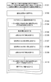
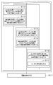
- FIG. 1 is a drawing schematically showing a structure of a group III nitride semiconductor device according to the present embodiment and a structure of an epitaxial substrate for the group III nitride semiconductor device.
- FIG. 2 is a drawing showing main steps in the method of manufacturing a group III nitride semiconductor device and an epitaxial substrate according to the present embodiment.
- FIG. 3 is a drawing showing main steps in the method of manufacturing a group III nitride semiconductor device and an epitaxial substrate according to the present embodiment.
- FIG. 4 is a drawing schematically showing products in main steps in the method of manufacturing a group III nitride semiconductor device and an epitaxial substrate according to the present embodiment.
- FIG. 1 is a drawing schematically showing a structure of a group III nitride semiconductor device according to the present embodiment and a structure of an epitaxial substrate for the group III nitride semiconductor device.
- FIG. 2 is a drawing showing main steps in the method of manufacturing a group III nit
- FIG. 5 is a drawing schematically showing products in main steps in the method of manufacturing a group III nitride semiconductor device and an epitaxial substrate according to the present embodiment.
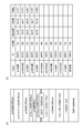
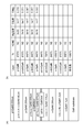
- FIG. 6 is a drawing showing the element structure of the laser diode of Example 1, and the atmospheric gas, p-type dopant concentration, oxygen concentration and O / Mg ratio of the epitaxial structure layer for this element.
- FIG. 7 is a drawing showing the element structure of the laser diode of Example 2, and the atmospheric gas, p-type dopant concentration, oxygen concentration and O / Mg ratio of the epitaxial structure layer for this element.
- FIG. 6 is a drawing showing the element structure of the laser diode of Example 1, and the atmospheric gas, p-type dopant concentration, oxygen concentration and O / Mg ratio of the epitaxial structure layer for this element.
- FIG. 7 is a drawing showing the element structure of the laser diode of Example 2, and the atmospheric gas, p-type dopant concentration, oxygen concentration and O / Mg
- FIG. 8 is a drawing showing the element structure of the laser diode of Example 3, and the atmospheric gas, p-type dopant concentration, oxygen concentration and O / Mg ratio of the epitaxial structure layer for this element.
- FIG. 9 is a drawing showing the element structure of the laser diode of Example 4, and the atmospheric gas, p-type dopant concentration, oxygen concentration and O / Mg ratio of the epitaxial structure layer for this element.
- FIG. 10 is a drawing showing the element structure of the laser diode of Example 5 and the atmospheric gas in the constituent layers of the epitaxial structure.
- FIG. 1 is a drawing schematically showing the structure of a group III nitride semiconductor device and the structure of an epitaxial substrate for the group III nitride semiconductor device according to the present embodiment.
- a light emitting element such as a light emitting diode or a laser diode will be described as the group III nitride semiconductor element 11, but the present embodiment is applied to a group III nitride semiconductor element including a p-type group III nitride semiconductor. Applicable.
- Epitaxial substrate EP has an epitaxial layer structure similar to that of group III nitride semiconductor device 11. In the following description, a semiconductor layer constituting the group III nitride semiconductor device 11 will be described.
- the epitaxial substrate EP includes semiconductor layers (semiconductor films) corresponding to these semiconductor layers, and the description is applied to the corresponding semiconductor layers for the group III nitride semiconductor element 11.
- a coordinate system S and a crystal coordinate system CR are shown.
- the main surface 13a of the substrate 13 faces the Z-axis direction and extends in the X direction and the Y direction.
- the X axis is in the direction of the a axis.
- the group III nitride semiconductor device 11 includes a substrate 13 and an n-type group III nitride semiconductor epitaxial region (hereinafter referred to as “n-type group III nitride semiconductor region”). ) 15, a light emitting layer 17, and a p-type group III nitride semiconductor epitaxial region (hereinafter referred to as “p-type group III nitride semiconductor region”) 19.
- the substrate 13 has a main surface 13a made of a first gallium nitride-based semiconductor and exhibits conductivity.
- the main surface 13a of the substrate 13 is inclined at an angle in the range of 50 degrees or more and less than 130 degrees from the plane Sc perpendicular to the reference axis Cx extending along the c axis of the first gallium nitride semiconductor.
- the n-type group III nitride semiconductor region 15 includes one or a plurality of n-type gallium nitride semiconductor layers and can be provided on the main surface 13a.
- the n-type group III nitride semiconductor region 15 can include, for example, an n-type buffer layer, an n-type cladding layer, and an n-type light guide layer.
- the p-type group III nitride semiconductor region 19 can include one or more p-type gallium nitride based semiconductor layers.
- the p-type group III nitride semiconductor region 19 includes, for example, a first p-type gallium nitride semiconductor layer 21 and is provided on the main surface 13a.
- the oxygen concentration of the first p-type gallium nitride based semiconductor layer 21 is 5 ⁇ 10 17 cm ⁇ 3 or less.
- the concentration ratio (Noxg / Npd) between the p-type dopant concentration Npd and the oxygen concentration Noxg of the first p-type gallium nitride based semiconductor layer 21 is 1/10 or less.
- the group III nitride semiconductor region 19 can include the second p-type gallium nitride based semiconductor layer 23.
- the p-type group III nitride semiconductor region 19 can include, for example, a p-type electron block layer, a p-type light guide layer, a p-type cladding layer, and a p-type contact layer.
- the first p-type gallium nitride based semiconductor layer 21 is provided on the main surface 13 a of the substrate 13.
- the main surface 13a is inclined at an angle in the range of 50 degrees or more and less than 130 degrees with respect to the surface Sc orthogonal to the reference axis Cx. Since the oxygen concentration in the first p-type gallium nitride based semiconductor layer 21 is 5 ⁇ 10 17 cm ⁇ 3 or less, the oxygen contained in the first p-type gallium nitride based semiconductor layer 21 causes the first p-type gallium nitride based semiconductor layer 21. Compensation of the p-type dopant in the semiconductor layer 21 can be reduced. Further, since the concentration ratio (Noxg / Npd) is 1/10 or less, the p-type dopant concentration Npd can be lowered.
- the first and second p-type gallium nitride based semiconductor layers 21 and 23 can be made of GaN, InGaN, AlGaN or InAlGaN.
- the oxygen concentration is reduced and the concentration ratio (Noxg / Npd) is reduced to 1/10 or less. Is done.
- the first p-type gallium nitride based semiconductor layer 21 preferably does not contain indium as a group III constituent element. Thereby, in the gallium nitride based semiconductor not containing indium as a group III constituent element, the oxygen concentration can be reduced and the p-type dopant concentration Npd can be lowered.
- the first p-type gallium nitride based semiconductor layer 21 can be made of GaN or AlGaN. In GaN or AlGaN grown on a non-polar group III nitride semiconductor surface, the oxygen concentration is reduced and the concentration ratio (Noxg / Npd) is reduced to 1/10 or less.
- the second p-type gallium nitride based semiconductor layer 23 preferably contains indium as a group III constituent element.
- the oxygen concentration can be reduced and the p-type dopant concentration Npd can be lowered.
- the oxygen concentration of the second p-type gallium nitride based semiconductor layer 23 can be 5 ⁇ 10 17 cm ⁇ 3 or less.
- the second p-type gallium nitride based semiconductor layer 23 contains indium as a group III constituent element and can be made of, for example, InGaN or InAlGaN.
- the concentration ratio (Noxg / Npd) between the p-type dopant concentration Npd and the oxygen concentration Noxg can be 1/10 or less. Also in the p-type gallium nitride based semiconductor layer 23 containing indium as a group III constituent element, the oxygen concentration can be reduced and the concentration ratio (Noxg / Npd) can be reduced to 1/10 or less. Therefore, the characteristics of the p-type group III nitride semiconductor can be improved.
- the p-type dopant concentration is, for example, 1 ⁇ 10 18 cm ⁇ . This is because it is preferably 3 or more, and if the doping concentration is less than this, the resistance increases and the electrical characteristics deteriorate.
- the p-type dopant concentration is preferably 5 ⁇ 10 19 cm ⁇ 3 or less, for example, if the doping concentration is higher than this, the crystallinity deteriorates and the electrical characteristics deteriorate.
- the p-type dopant concentration in these layers 21 and 23 can be made smaller than the p-type dopant concentration in the p-type contact layer 25.
- the p-type group III nitride semiconductor stack 26 is composed of two layers of first and second p-type gallium nitride based semiconductor layers 21 and 23.
- the p-type group III nitride semiconductor stack 26 forms the first junction J1 with the contact layer 25 and the light emitting layer 17 and the second junction J2.
- the oxygen concentration is preferably 5 ⁇ 10 17 cm ⁇ 3 or less over the entire p-type group III nitride semiconductor stack 26.
- the concentration ratio (Noxg / Npd) between the p-type dopant concentration Npd of the group III nitride semiconductor stack 26 and the oxygen concentration Noxg can be 1/10 or less.
- the oxygen concentration is reduced and the ratio (Noxg / Npd) is reduced to 1/10 or less.
- the electrical characteristics of the p-type group III nitride semiconductor constituting the current path from the anode can be improved.
- the carbon concentration of the first p-type gallium nitride based semiconductor layer 21 can be 1 ⁇ 10 17 cm ⁇ 3 or less.
- the concentration of carbon impurities increases in the first p-type gallium nitride based semiconductor layer 21 grown in a nitrogen atmosphere.
- not only the oxygen concentration but also the carbon concentration can be reduced.
- the carbon concentration of the second p-type gallium nitride based semiconductor layer 23 can be 1 ⁇ 10 17 cm ⁇ 3 or less.
- the substrate 13 is made of a first gallium nitride based semiconductor, and can be, for example, GaN, InGaN, AlGaN, or the like. Since GaN is a gallium nitride semiconductor that is a binary compound, it can provide good crystal quality and a stable substrate main surface. Further, the first gallium nitride based semiconductor can be made of, for example, AlN.
- the c-plane of the substrate 13 extends along the plane Sc shown in FIG.
- a coordinate system CR c-axis, a-axis, m-axis
- the main surface 13a of the substrate 13 is inclined at an inclination angle ⁇ in the direction of the m-axis or a-axis of the first gallium nitride semiconductor with respect to a plane orthogonal to the reference axis Cx.
- the inclination angle ⁇ is defined by the angle formed between the normal vector VN of the principal surface 13a of the substrate 13 and the c-axis part vector VC indicating the reference axis Cx.
- the active layer 17 is provided between the n-type gallium nitride semiconductor region 15 and the p-type gallium nitride semiconductor region 19, and the n-type gallium nitride semiconductor region 15, the active layer 17, and the p-type
- the gallium nitride based semiconductor region 19 is arranged in the direction of the normal axis Ax.
- the range of the inclination angle ⁇ can be divided into a first angle range of surface orientation showing semipolar characteristics and a second angle range of surface orientation showing characteristics close to nonpolarity.
- the first angle range is, for example, 50 degrees or more and 80 degrees or less, and is 100 degrees or more and less than 130 degrees.
- the crystallinity of InGaN having a particularly high In composition can be enhanced
- the second angle range there is an advantage that a piezoelectric field of InGaN having a particularly high In composition can be suppressed.
- the light emitting layer 17 includes an active layer 27, and may include an n-side light guide layer 29 and a p-side light guide layer 31, if necessary.
- the active layer 27 includes at least one semiconductor epitaxial layer 33.
- the semiconductor epitaxial layer 33 is provided on the gallium nitride based semiconductor epitaxial region 15.
- the semiconductor epitaxial layer 33 is made of, for example, AlGaN, GaN, InGaN, InAlGaN, or the like, and can be made of a second gallium nitride based semiconductor containing indium.
- the active layer 27 can include another semiconductor epitaxial layer 35.
- the other semiconductor epitaxial layer 35 is made of, for example, AlGaN, GaN, InGaN, InAlGaN, or the like, and can be made of a third gallium nitride based semiconductor containing indium.
- Another semiconductor epitaxial layer 35 has a band gap larger than that of the semiconductor epitaxial layer 33.
- the semiconductor epitaxial layer 33 serves as a well layer and the semiconductor epitaxial layer 35 serves as a barrier layer.
- the active layer 27 can have a single or multiple quantum well structure.
- the emission wavelength of the light emitting layer 17 (active layer 27) can be, for example, not less than 440 nm and not more than 600 nm. In the light-emitting element that generates light in the above-described emission wavelength range, the electrical characteristics of the p-type gallium nitride semiconductor can be improved.
- the emission wavelength of the light emitting layer 17 (active layer 27) can be not less than 490 nm and not more than 600 nm. Thereby, the characteristics of the p-type gallium nitride semiconductor can be improved in a light-emitting element that provides light emission at a long wavelength.
- Semiconductor layer 15 n-type InAlGaN cladding layer.
- Semiconductor layer 21 p-type GaN electron block layer.
- Semiconductor layer 23 p-type InAlGaN cladding layer.
- Semiconductor layer 25 p-type GaN contact layer.
- Semiconductor layer 29 n-side undoped InGaN light guide layer.
- Semiconductor layer 31 p-side undoped InGaN light guide layer.
- the n-type group III nitride semiconductor region 15 can include an n-side light guide layer 29 and an n-type light guide layer
- the p-type group III nitride semiconductor region 19 includes a p-side light guide layer.
- a guide layer 31 and a p-type light guide layer may be included.
- the epitaxial substrate EP of the group III nitride semiconductor element 11 includes semiconductor layers (semiconductor films) corresponding to these semiconductor layers, and the description applies to the corresponding semiconductor layer for the group III nitride semiconductor element 11.
- the surface roughness of the epitaxial substrate EP is 1 nm or less in terms of arithmetic average roughness.
- the group III nitride semiconductor device 11 can include a first electrode 37 (for example, an anode) provided on the contact layer 25, and the first electrode 37 is an opening of the insulating film 39 that covers the contact layer 25.
- a contact JC is formed on the p-type group III nitride semiconductor region 19 (contact layer 25) through 39a.
- Ni / Au is used as the electrode.
- the group III nitride semiconductor device 11 can include a second electrode 41 (for example, a cathode) provided on the back surface 13b of the substrate 13, and the second electrode 41 is made of, for example, Ti / Al.
- FIGS. 2 and 3 are drawings showing main steps in the method of manufacturing the group III nitride semiconductor device and the epitaxial substrate according to the present embodiment.
- 4 and 5 are drawings schematically showing products in main steps in the method of manufacturing a group III nitride semiconductor device and an epitaxial substrate according to the present embodiment.
- an epitaxial substrate and a group III nitride semiconductor optical device having a light emitting device structure were fabricated on the substrate by metal organic vapor phase epitaxy.
- Use as a raw material for epitaxial growth trimethyl gallium (TMG), trimethyl indium (TMI), trimethyl aluminum (TMA), ammonia (NH 3), silane (SiH 4), biscyclopentadienyl magnesium (Cp 2 Mg) It was.
- a substrate (substrate 51 shown in FIG. 4A) having a main surface made of a gallium nitride semiconductor is prepared.
- the normal axis of the principal surface of the substrate 51 has an inclination angle within an angle range of 50 degrees to less than 130 degrees with respect to the c-axis of the gallium nitride semiconductor.
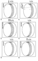
- the substrate 51 has a main surface that is inclined at an angle of 75 degrees from the c-plane in the m-axis direction in hexagonal GaN, and this inclined surface is shown as a ⁇ 20-21) plane.
- the main surface is mirror-polished.
- step S ⁇ b> 102 the substrate 51 is installed in the growth furnace 10.
- a quartz jig such as a quartz flow channel is disposed in the growth furnace 10. If necessary, heat treatment is performed for 10 minutes while supplying a heat treatment gas containing NH 3 and H 2 to the growth furnace 10 at a temperature of 1050 degrees Celsius and an in-furnace pressure of 27 kPa. This heat treatment causes surface modification.
- a group III nitride semiconductor layer is grown on the substrate 51 to form an epitaxial substrate.
- a source material for a group III constituent element and a group V constituent element, a source gas containing an n-type dopant, and an atmosphere gas are supplied to the growth reactor 10 to epitaxially form the group III nitride semiconductor region 53. grow up.
- the inclination angle of main surface 53 a of group III nitride semiconductor region 53 corresponds to the inclination angle of main surface 51 a of substrate 51.
- the group III nitride semiconductor region 53 can include one or more group III nitride semiconductor layers.
- the atmospheric gas includes a carrier gas and a subflow gas.
- the atmospheric gas can include, for example, nitrogen and / or hydrogen.
- the following gallium nitride based semiconductor regions are grown.
- TMG, NH 3 , SiH 4 and nitrogen and / or hydrogen are supplied to the growth reactor 10 to grow the Si-doped GaN layer 55a.
- TMG, TMI, TMA, NH 3 , SiH 4 and nitrogen are supplied to the growth reactor 10 at a substrate temperature of 870 degrees Celsius to grow the Si-doped InAlGaN layer 55b.
- TMG, NH 3 , SiH 4 and nitrogen and / or hydrogen are supplied to the growth reactor 10 to grow the Si-doped GaN layer 55c.
- oxygen tends to be desorbed from jigs in the growth furnace and deposits on the jigs.
- step S105 the light emitting layer 57 is grown.
- TMG, TMI, NH 3 and nitrogen are supplied to the growth reactor at a substrate temperature of 870 degrees Celsius to grow the InGaN optical guide layer 59a.
- Part or all of the light guide layer 59a may be undoped or n-type conductive.
- the active layer 59b is grown.
- TMG, TMI, NH 3 and nitrogen of the atmospheric gas are supplied to the growth furnace to grow the undoped InGaN barrier layer 61a.
- the thickness of the InGaN layer 61a is 15 nm.
- the growth is interrupted, and the substrate temperature is changed from the growth temperature of the barrier layer to the growth temperature of the well layer.
- TMG, TMI, NH 3 and nitrogen of the atmospheric gas are supplied to the growth reactor 10 to grow the undoped InGaN well layer 61b.
- the thickness of the InGaN well layer 61b is 3 nm.
- the quantum well structure includes three well layers.
- TMG, TMI, NH 3 and nitrogen of the atmospheric gas are supplied to the growth reactor 10 at a substrate temperature of 870 degrees Celsius to grow the InGaN optical guide layer 59c.
- a part or all of the light guide layer 59c may be undoped or p-type conductive.
- the inclination angles of the main surfaces of the light emitting layer 57 and the active layer 59 b correspond to the inclination angles of the main surface 51 a of the substrate 51.
- step S110 a group III source material, a group V source material, a source gas containing a p-type dopant, and an atmosphere gas are supplied to the growth reactor 10, and the group III nitride semiconductor region 63 is epitaxially grown.
- the inclination angle of main surface 63 a of group III nitride semiconductor region 63 corresponds to the inclination angle of main surface 51 a of substrate 51.
- the group III nitride semiconductor region 63 can include one or more group III nitride semiconductor layers. In this embodiment, the following gallium nitride based semiconductor regions are grown.
- TMG the supply of TMG is stopped and the substrate temperature is raised.
- TMG, NH 3 , Cp 2 Mg, and atmospheric gas are supplied to the growth furnace to grow the p-type GaN electron block layer 65a at a substrate temperature of 840 degrees Celsius.
- nitrogen as an atmospheric gas is preferably supplied.
- TMG, TMI, NH 3 , Cp 2 Mg and nitrogen are supplied to the growth reactor 10 to grow the Mg-doped InGaN optical guide layer 65b at a substrate temperature of 840 degrees Celsius.
- TMG, NH 3 , Cp 2 Mg, and atmospheric gas are supplied to the growth reactor 10 to grow the Mg-doped GaN optical guide layer 65c.
- nitrogen is preferably supplied as an atmospheric gas.
- TMG, TMI, TMA, NH 3 , Cp 2 Mg and nitrogen are supplied to the growth reactor 10 at a substrate temperature of 870 degrees Celsius to grow the Mg-doped InAlGaN cladding layer 65d.
- TMG, NH 3 , Cp 2 Mg, and atmospheric gas are supplied to the growth reactor 10 to grow the high-concentration Mg-doped GaN contact layer 65e.
- nitrogen is preferably supplied as an atmospheric gas.
- an electrode is formed on the epitaxial substrate EP1.
- the electrode is formed as follows. For example, an electrode (Ni / Au) is formed on the p-type GaN contact layer 65e, and an electrode (Ti / Al) is formed on the back surface of the epitaxial substrate EP1. Prior to the formation of the electrodes, the epitaxial substrate EP1 can be processed to form a ridge structure.
- step S110 The epitaxial growth of the p-type group III nitride semiconductor region 63 in step S110 can be performed as follows as shown in FIG.
- the group III nitride semiconductor region 63 includes one or more p-type gallium nitride semiconductor layers (referred to as “p-type gallium nitride semiconductor layer 63A”) containing indium as a group III constituent element, and / or Alternatively, it may include one or more p-type gallium nitride semiconductor layers (referred to as “p-type gallium nitride semiconductor layer 63B”) that do not contain indium as a group III constituent element. As shown in FIG. 5A, in step S112, all of the p-type gallium nitride based semiconductor layer 63A is formed in a nitrogen atmosphere.
- the oxygen concentration of the p-type gallium nitride based semiconductor layer 63A is 5 ⁇ 10 17 cm ⁇ 3 or less, and the ratio (Noxg) between the p-type dopant concentration Npd of the p-type gallium nitride based semiconductor layer 63A and the oxygen concentration Noxg / Npd) is 1/10 or less.
- step S113 a part of the p-type gallium nitride based semiconductor layer 63B is formed in a nitrogen atmosphere.
- the oxygen concentration of the p-type gallium nitride based semiconductor layer 63C is 5 ⁇ 10 17 cm ⁇ 3 or less, and the ratio of the p-type dopant concentration Npd of the p-type gallium nitride based semiconductor layer 63C to the oxygen concentration Noxg (Noxg / Npd) is 1/10 or less.
- a step of forming the remaining layer 63D of the p-type gallium nitride based semiconductor layer 63B in a hydrogen atmosphere is performed. In the growth of the group III nitride semiconductor region 63, the order of the growth of the layers 63A, 63C, and 63D can be changed.
- the group III nitride semiconductor region 65 includes one or more p-type gallium nitride semiconductor layers (referred to as “p-type gallium nitride semiconductor layer 65A”) containing indium as a group III constituent element;
- p-type gallium nitride semiconductor layer 65B One or a plurality of p-type gallium nitride semiconductor layers not containing indium as a group III constituent element (referred to as “p-type gallium nitride semiconductor layer 65B”) can be included.
- p-type gallium nitride semiconductor layer 65A containing indium as a group III constituent element
- p-type gallium nitride semiconductor layer 65B One or a plurality of p-type gallium nitride semiconductor layers not containing indium as a group III constituent element
- the oxygen concentration of the p-type gallium nitride based semiconductor layer 65A is 5 ⁇ 10 17 cm ⁇ 3 or less, and the ratio of the p-type dopant concentration Npd of the p-type gallium nitride based semiconductor layer 65A to the oxygen concentration Noxg (Noxg / Npd) is 1/10 or less.
- the p-type gallium nitride based semiconductor layer 65B is formed in a nitrogen atmosphere.
- the oxygen concentration of the p-type gallium nitride based semiconductor layer 65B is 5 ⁇ 10 17 cm ⁇ 3 or less, and the ratio of the p-type dopant concentration Npd of the p-type gallium nitride based semiconductor layer 65B to the oxygen concentration Noxg (Noxg / Npd) is 1/10 or less.
- the order of the growth of the layers 65A and 65B can be rearranged.
- the group III nitride semiconductor region 67 includes one or more p-type gallium nitride based semiconductor layers containing indium as a group III constituent element (referred to as “p-type gallium nitride based semiconductor layer 67A”). And one or a plurality of p-type gallium nitride semiconductor layers (referred to as “p-type gallium nitride semiconductor layer 67B”) that do not contain indium as a group III constituent element, and a p-type contact layer 67C. As shown in FIG.
- step S116 all of the p-type gallium nitride based semiconductor layer 67A is formed in a nitrogen atmosphere, and all of the p-type gallium nitride based semiconductor layer 67B is formed in a nitrogen atmosphere.
- the oxygen concentration of these layers 67A and 67B is 5 ⁇ 10 17 cm ⁇ 3 or less, and the p-type dopant concentration of these layers 67A and 67B
- the ratio of Npd to oxygen concentration Noxg Noxg (Noxg / Npd) is 1/10 or less.
- a p-type gallium nitride based semiconductor contact layer 67C is formed.
- the contact layer 67C can also be formed in a nitrogen atmosphere. In this growth, the oxygen concentration of the contact layer 67C is 5 ⁇ 10 17 cm ⁇ 3 or less.
- the quartz tube of the growth furnace is supplied with source gas and atmospheric gas for the group III constituent element and the group V constituent element.
- the ratio of the atmospheric gas can be 60% or more.
- the percentage is volume percent.
- Example 1 A laser diode having the element structure shown in part (a) of FIG. 6 is manufactured.
- FIG. 6B the atmospheric gas of the constituent layer of the epitaxial structure is shown.
- a ⁇ 20-21 ⁇ plane GaN substrate is prepared.
- An epitaxial stack is formed on the GaN substrate by metal organic vapor phase epitaxy.
- the growth of the p-type gallium nitride semiconductor layer the growth of the gallium nitride semiconductor layer not containing indium (In) is performed in a hydrogen atmosphere formed by supplying only hydrogen as an atmospheric gas.
- the gallium nitride based semiconductor layer containing indium (In) is grown in a nitrogen atmosphere formed by supplying only nitrogen as the atmospheric gas.
- An insulating film (silicon oxide film) having a stripe window with a width of 10 ⁇ m is formed on the epitaxial layer.
- a Pd electrode is formed by vapor deposition as an anode electrode. Thereafter, a pad electrode is formed by vapor deposition.
- the substrate products thus produced are separated at 600 ⁇ m intervals to produce laser bars.
- a reflective film made of a dielectric multilayer film is formed on the cavity end face of the laser bar.
- the dielectric multilayer film is made of SiO 2 / TiO 2 .
- the reflectance of the front end face is 80%, and the reflectance of the rear end face is 95%. It oscillates at a wavelength of 520 nm and a threshold current of 4 kA / cm 2 , and the operating voltage is 8.5 volts.
- the magnesium concentration, the oxygen concentration, and the O / Mg ratio are shown.
- “3e20” represents 3 ⁇ 10 20 .
- a gallium nitride based semiconductor layer containing indium (In), for example, p-type InGaN or p-type InAlGaN is grown in a nitrogen atmosphere formed by supplying only nitrogen as an atmospheric gas, and the oxygen concentration is 5 ⁇ 10 17 cm ⁇ 3 or less
- the O / Mg ratio is 0.1 or less.
- the film forming conditions are such that the V / III ratio is about 5000 to 10,000.
- the oxygen concentration is high.
- Example 2 A laser diode having the element structure shown in part (a) of FIG. 7 is manufactured.
- part (b) of FIG. 7 the atmospheric gas of the constituent layer of the epitaxial structure is shown.
- a ⁇ 20-21 ⁇ plane GaN substrate is prepared.
- An epitaxial stack is formed on the GaN substrate by metal organic vapor phase epitaxy.
- the gallium nitride semiconductor layer not containing indium (In) is grown in an atmosphere formed by supplying nitrogen or hydrogen as an atmosphere gas.
- the gallium nitride based semiconductor layer containing indium (In) is grown in an atmosphere formed by supplying only nitrogen as an atmosphere gas.
- an insulating film, an anode electrode, and the like are produced on the epitaxial stack to produce a substrate product.
- This substrate product is separated at 600 ⁇ m intervals to produce laser bars.
- a reflective film made of a dielectric multilayer film is formed on the cavity end face of the laser bar. It oscillates at a wavelength of 520 nm and a threshold current of 4 kA / cm 2 , and the operating voltage is 8.0 volts.
- the magnesium concentration, the oxygen concentration, and the O / Mg ratio are shown.
- a gallium nitride based semiconductor layer containing indium (In), for example, p-type InGaN and p-type InAlGaN is grown in a nitrogen atmosphere formed by supplying only nitrogen as an atmospheric gas, and the O / Mg ratio is 0.1 or less.
- the film forming conditions are such that the V / III ratio is about 5000 to 10,000.
- a gallium nitride based semiconductor layer not containing indium (In), for example, a p-type GaN optical guide layer is formed by supplying only nitrogen as an atmospheric gas, while the remaining gallium nitride not containing indium (In).
- the growth of the system semiconductor layer, for example, the p + type GaN contact layer and the p type GaN electron block layer is performed in a hydrogen atmosphere.
- the oxygen concentration is low and the O / Mg ratio is 0.1 or less.
- the oxygen concentration is high.
- Example 3 A laser diode having the element structure shown in FIG. 8A is manufactured. Part (b) of FIG. 8 shows the atmospheric gas of the constituent layer of the epitaxial structure.
- a ⁇ 20-21 ⁇ plane GaN substrate is prepared.
- An epitaxial stack is formed on the GaN substrate by metal organic vapor phase epitaxy.
- the gallium nitride semiconductor layer not containing indium (In) is grown in an atmosphere formed by supplying nitrogen or hydrogen as an atmosphere gas.
- the gallium nitride based semiconductor layer containing indium (In) is grown in a nitrogen atmosphere formed by supplying only nitrogen as the atmospheric gas.
- an insulating film, an anode electrode, and the like are produced on the epitaxial stack to produce a substrate product.
- This substrate product is separated at 600 ⁇ m intervals to produce laser bars.
- a reflective film made of a dielectric multilayer film is formed on the cavity end face of the laser bar. It oscillates at a wavelength of 520 nm and a threshold current of 4 kA / cm 2 , and the operating voltage is 7.5 volts.
- the magnesium concentration, the oxygen concentration, and the O / Mg ratio oxygen concentration / magnesium concentration
- the growth of a gallium nitride based semiconductor layer not containing indium (In), for example, a p-type GaN optical guide layer and a p-type GaN electron block layer, is formed by supplying only nitrogen as an atmospheric gas, while the remaining indium (
- the growth of a gallium nitride based semiconductor layer not containing In), for example, a p + type GaN contact layer, is grown in a hydrogen atmosphere.
- the oxygen concentration is low and the O / Mg ratio is 0.1 or less.
- the film forming conditions are such that the V / III ratio is about 5000 to 10,000.
- the oxygen concentration is high.
- Example 4 A laser diode having the element structure shown in part (a) of FIG. 9 is produced.
- part (b) of FIG. 9 the atmospheric gas of the constituent layer of the epitaxial structure is shown.
- a ⁇ 20-21 ⁇ plane GaN substrate is prepared.
- An epitaxial stack is formed on the GaN substrate by metal organic vapor phase epitaxy.
- the growth of the p-type gallium nitride semiconductor layer the growth of the gallium nitride semiconductor layer not containing indium (In) is performed in a nitrogen atmosphere formed by supplying only nitrogen as the atmospheric gas.
- the gallium nitride based semiconductor layer containing indium (In) is grown in a nitrogen atmosphere formed by supplying only nitrogen as the atmospheric gas.
- an insulating film, an anode electrode, and the like are produced on the epitaxial stack to produce a substrate product.
- This substrate product is separated at 600 ⁇ m intervals to produce laser bars.
- a reflective film made of a dielectric multilayer film is formed on the cavity end face of the laser bar. It oscillates at a wavelength of 520 nm and a threshold current of 4 kA / cm 2 , and the operating voltage is 7.0 volts.
- the magnesium concentration, the oxygen concentration, and the O / Mg ratio oxygen concentration / magnesium concentration
- the film forming conditions are such that the V / III ratio is about 5000 to 10,000.
- a gallium nitride based semiconductor layer not containing indium (In), for example, a p-type GaN optical guide layer, a p-type GaN electron blocking layer, and a P + GaN contact layer is formed by supplying only nitrogen as an atmospheric gas, and is all p-type.
- the gallium nitride based semiconductor layer is grown in a nitrogen atmosphere.
- the oxygen concentration is low and the O / Mg ratio is 0.1 or less.
- Example 5 A laser diode having the element structure shown in part (a) of FIG. 10 is produced.
- FIG. 10B the atmospheric gas of the constituent layer of the epitaxial structure is shown.
- a ⁇ 20-21 ⁇ plane GaN substrate is prepared.
- An epitaxial stack is formed on the GaN substrate by metal organic vapor phase epitaxy.
- the growth of the gallium nitride based semiconductor layer not containing indium (In) and the growth of the gallium nitride based semiconductor layer containing indium (In) are performed in a nitrogen atmosphere formed by supplying only nitrogen as the atmospheric gas. .
- the surface roughness of the epitaxial substrate is 1 nm or less in terms of arithmetic average roughness.
- Example 2 In the same manner as in Example 1, an insulating film, an anode electrode, and the like are produced on the epitaxial stack to produce a substrate product. This substrate product is separated at 600 ⁇ m intervals to produce laser bars. A reflective film made of a dielectric multilayer film is formed on the cavity end face of the laser bar in the same manner as in the first embodiment. It oscillates at a threshold current of 4 kA / cm 2 at a wavelength of 520 nm, and the operating voltage is 6.5 volts.
- the growth of the p-type and n-type gallium nitride semiconductor layers is formed by supplying only nitrogen as the atmospheric gas.
- the oxygen concentration is low and the O / Mg ratio is 0.1 or less.
- the following technical contributions can be obtained. For example, the number of times the carrier gas is switched is reduced, and dust such as particles generated during growth is reduced. Also, impurities at the interface are reduced. Since a nitrogen carrier gas is used, the epitaxial surface is planarized and the surface morphology is improved. This improves chip yield and device reliability. Furthermore, the growth temperature of the p-type semiconductor layer can be lowered, and the deterioration of the well layer during the growth of the p-type semiconductor layer is reduced.
- the growth of the p-type gallium nitride based semiconductor layer grown therein has an O / Mg ratio of 0.1 or less.
- the inventors have tried various measures for reducing the oxygen concentration, such as selection of a high-purity raw material, substrate cleaning before epitaxial growth, and jig cleaning, but none of them has a sufficient effect.
- the semipolar plane shows oxygen uptake that is about one digit higher than the c-plane. For this reason, in the growth on the c-plane, the incorporation of oxygen impurities does not greatly affect the quality of the epitaxially grown film. However, the growth to the semipolar plane is a cause of deteriorating the electrical characteristics of the p-type semiconductor layer.
- the gallium nitride based semiconductor layer containing In is grown in a nitrogen atmosphere, and the oxygen concentration of the gallium nitride based semiconductor layer is grown in other hydrogen atmospheres. It has been found that the oxygen concentration is lower than that of the layer containing no oxygen. Therefore, when a gallium nitride based semiconductor layer not containing In is grown in a nitrogen atmosphere, the oxygen concentration of the gallium nitride based semiconductor layer can be reduced. Thereby, the internal resistance of the semiconductor element can be lowered. According to experiments, the oxygen concentration of the gallium nitride based semiconductor layer grown in a nitrogen atmosphere can be reduced, and a low-resistance semiconductor element can be manufactured.
- the oxygen supply source is an impurity in a gas such as a raw material supplied to the growth furnace and other jigs.
- a gas such as a raw material supplied to the growth furnace and other jigs.
- oxygen concentration in the raw material serve as a supply source of oxygen
- oxygen incorporation coefficient into the crystal are considered as factors.
- the oxygen concentration in the epitaxial semiconductor crystal increases in either a hydrogen atmosphere or a nitrogen atmosphere. From this result, it is considered that “the oxygen uptake coefficient into the crystal” does not depend on the atmospheric gas.
- the factors are “oxygen source” such as jigs, depots and cleaning agent residues in the furnace, "oxygen desorption coefficient from the oxygen source”, “incorporation of oxygen into the crystal” "Coefficient” is considered.
- oxygen uptake coefficient into the crystal does not depend on the atmospheric gas. Therefore, the remaining “oxygen incorporation coefficient into the crystal” varies depending on the atmospheric gas.
- Hydrogen is a reducing gas and desorbs oxygen from unwanted deposits such as depots. It is considered that this oxygen is taken into the epitaxial crystal. Therefore, it is preferable to use nitrogen as the atmospheric gas (carrier gas and subflow gas).
- a group III nitride semiconductor device having a p-type gallium nitride based semiconductor layer with a reduced oxygen concentration is provided.
- a method for manufacturing a group III nitride semiconductor device that can reduce the amount of oxygen impurities taken in is provided.
- an epitaxial substrate for a group III nitride semiconductor device is provided.
- semiconductor epitaxial layer 35 ... semiconductor epitaxial layer, 37 ... first electrode, 39 ... insulating film, JC ... Contact, 41 ... Second electrode, 51 ... Substrate, 53 ... Group III nitride semiconductor region, 55a ... Si-doped GaN layer, 55b ... Si-doped InAlGaN layer, 55c ... Si-doped GaN layer, 59a ... InGaN light guide layer 59b ... Active layer, 59c ... InGaN light guide layer, 61a ... Undoped InGaN barrier layer, 61b ... Undoped InGaN well layer, 65a ... p-type GaN electron blocking layer, 65b ...
- Mg-doped InGaN light guide layer 65c ... Mg-doped GaN light Guide layer, 65d ... Mg-doped InAlGaN cladding layer, 65e ... high-concentration Mg-doped GaN contact layer, EP1 ... epitaxial substrate.
Landscapes
- Engineering & Computer Science (AREA)
- Physics & Mathematics (AREA)
- Condensed Matter Physics & Semiconductors (AREA)
- General Physics & Mathematics (AREA)
- Optics & Photonics (AREA)
- Power Engineering (AREA)
- Microelectronics & Electronic Packaging (AREA)
- Computer Hardware Design (AREA)
- Manufacturing & Machinery (AREA)
- Chemical & Material Sciences (AREA)
- Nanotechnology (AREA)
- Electromagnetism (AREA)
- Crystallography & Structural Chemistry (AREA)
- Biophysics (AREA)
- Life Sciences & Earth Sciences (AREA)
- Materials Engineering (AREA)
- Led Devices (AREA)
- Semiconductor Lasers (AREA)
Priority Applications (2)
| Application Number | Priority Date | Filing Date | Title |
|---|---|---|---|
| EP11837949.4A EP2637267A1 (en) | 2010-11-05 | 2011-10-28 | Group iii nitride semiconductor device, method of manufacturing group iii nitride semiconductor devices, and epitaxial substrate |
| CN2011800534287A CN103190042A (zh) | 2010-11-05 | 2011-10-28 | Iii族氮化物半导体元件、制造iii族氮化物半导体元件的方法及外延基板 |
Applications Claiming Priority (2)
| Application Number | Priority Date | Filing Date | Title |
|---|---|---|---|
| JP2010248932A JP5842324B2 (ja) | 2010-11-05 | 2010-11-05 | Iii族窒化物半導体素子、iii族窒化物半導体素子を作製する方法、及びエピタキシャル基板 |
| JP2010-248932 | 2010-11-05 |
Publications (1)
| Publication Number | Publication Date |
|---|---|
| WO2012060299A1 true WO2012060299A1 (ja) | 2012-05-10 |
Family
ID=46018759
Family Applications (1)
| Application Number | Title | Priority Date | Filing Date |
|---|---|---|---|
| PCT/JP2011/074973 Ceased WO2012060299A1 (ja) | 2010-11-05 | 2011-10-28 | Iii族窒化物半導体素子、iii族窒化物半導体素子を作製する方法、及びエピタキシャル基板 |
Country Status (6)
| Country | Link |
|---|---|
| US (1) | US8809868B2 (enExample) |
| EP (1) | EP2637267A1 (enExample) |
| JP (1) | JP5842324B2 (enExample) |
| CN (1) | CN103190042A (enExample) |
| TW (1) | TW201234415A (enExample) |
| WO (1) | WO2012060299A1 (enExample) |
Cited By (1)
| Publication number | Priority date | Publication date | Assignee | Title |
|---|---|---|---|---|
| JP2021002575A (ja) * | 2019-06-21 | 2021-01-07 | 古河機械金属株式会社 | 構造体、光デバイス、光デバイスの製造方法、構造体の製造方法 |
Families Citing this family (14)
| Publication number | Priority date | Publication date | Assignee | Title |
|---|---|---|---|---|
| JP2821900B2 (ja) | 1989-04-05 | 1998-11-05 | 日本鉄道建設公団 | 音波制御装置を配置した輸送用高架構造物 |
| JP2820770B2 (ja) | 1990-04-19 | 1998-11-05 | 株式会社ブリヂストン | 干渉型防音装置 |
| JP5387302B2 (ja) * | 2009-09-30 | 2014-01-15 | 住友電気工業株式会社 | Iii族窒化物半導体レーザ素子、及びiii族窒化物半導体レーザ素子を作製する方法 |
| KR101659738B1 (ko) * | 2010-07-08 | 2016-09-26 | 엘지이노텍 주식회사 | 발광 소자 제조방법 |
| JP5361925B2 (ja) * | 2011-03-08 | 2013-12-04 | 株式会社東芝 | 半導体発光素子およびその製造方法 |
| JP6176141B2 (ja) * | 2014-02-19 | 2017-08-09 | 豊田合成株式会社 | Iii 族窒化物半導体発光素子の製造方法 |
| TWI577046B (zh) * | 2014-12-23 | 2017-04-01 | 錼創科技股份有限公司 | 半導體發光元件及其製作方法 |
| WO2019039189A1 (ja) * | 2017-08-24 | 2019-02-28 | 日本碍子株式会社 | 13族元素窒化物層、自立基板および機能素子 |
| US10665750B2 (en) | 2017-11-22 | 2020-05-26 | Epistar Corporation | Semiconductor device |
| CN110838514B (zh) * | 2018-08-17 | 2022-07-22 | 苏州能讯高能半导体有限公司 | 一种半导体器件的外延结构及其制备方法、半导体器件 |
| JP6744521B1 (ja) * | 2018-12-11 | 2020-08-19 | パナソニックセミコンダクターソリューションズ株式会社 | 窒化物系半導体発光素子及びその製造方法、並びに、窒化物系半導体結晶の製造方法 |
| US11527701B2 (en) * | 2019-10-28 | 2022-12-13 | Taiwan Semiconductor Manufacturing Company, Ltd. | Piezoelectric device and method of forming the same |
| JP7269190B2 (ja) * | 2020-02-27 | 2023-05-08 | 株式会社東芝 | 窒化物結晶、光学装置、半導体装置、窒化物結晶の製造方法 |
| US12482653B2 (en) * | 2020-09-30 | 2025-11-25 | Dynax Semiconductor, Inc. | Epitaxial structure of semiconductor device and method of manufacturing the same |
Citations (9)
| Publication number | Priority date | Publication date | Assignee | Title |
|---|---|---|---|---|
| JPH06209122A (ja) | 1992-11-20 | 1994-07-26 | Nichia Chem Ind Ltd | 窒化インジウムガリウム半導体の成長方法 |
| JP2004363622A (ja) * | 2004-07-16 | 2004-12-24 | Showa Denko Kk | GaN系化合物半導体の製造方法とGaN系化合物半導体製造用アンモニアおよびその製造方法 |
| WO2008117750A1 (ja) * | 2007-03-23 | 2008-10-02 | Tokuyama Corporation | P型iii族窒化物半導体およびiii族窒化物半導体素子 |
| WO2008153130A1 (ja) * | 2007-06-15 | 2008-12-18 | Rohm Co., Ltd. | 窒化物半導体発光素子及び窒化物半導体の製造方法 |
| WO2010041657A1 (ja) * | 2008-10-07 | 2010-04-15 | 住友電気工業株式会社 | 窒化ガリウム系半導体発光素子、窒化ガリウム系半導体発光素子を作製する方法、窒化ガリウム系発光ダイオード、エピタキシャルウエハ、及び窒化ガリウム系発光ダイオードを作製する方法 |
| WO2010090262A1 (ja) * | 2009-02-09 | 2010-08-12 | 住友電気工業株式会社 | エピタキシャルウエハ、窒化ガリウム系半導体デバイスを作製する方法、窒化ガリウム系半導体デバイス、及び酸化ガリウムウエハ |
| JP2010192865A (ja) * | 2009-01-23 | 2010-09-02 | Sumitomo Electric Ind Ltd | 窒化物半導体発光素子、エピタキシャル基板、及び窒化物半導体発光素子を作製する方法 |
| JP2010212651A (ja) * | 2009-09-08 | 2010-09-24 | Sumitomo Electric Ind Ltd | Iii族窒化物半導体素子、エピタキシャル基板、及びiii族窒化物半導体素子を作製する方法 |
| JP2010219490A (ja) * | 2009-02-20 | 2010-09-30 | Sumitomo Electric Ind Ltd | 窒化ガリウム系半導体膜を成長する方法、窒化ガリウム系半導体電子デバイスを作製する方法、エピタキシャル基板、及び窒化ガリウム系半導体電子デバイス |
Family Cites Families (1)
| Publication number | Priority date | Publication date | Assignee | Title |
|---|---|---|---|---|
| JP2005191530A (ja) * | 2003-12-03 | 2005-07-14 | Sumitomo Electric Ind Ltd | 発光装置 |
-
2010
- 2010-11-05 JP JP2010248932A patent/JP5842324B2/ja not_active Expired - Fee Related
-
2011
- 2011-10-28 EP EP11837949.4A patent/EP2637267A1/en not_active Withdrawn
- 2011-10-28 CN CN2011800534287A patent/CN103190042A/zh active Pending
- 2011-10-28 WO PCT/JP2011/074973 patent/WO2012060299A1/ja not_active Ceased
- 2011-11-04 US US13/289,813 patent/US8809868B2/en active Active
- 2011-11-04 TW TW100140401A patent/TW201234415A/zh unknown
Patent Citations (9)
| Publication number | Priority date | Publication date | Assignee | Title |
|---|---|---|---|---|
| JPH06209122A (ja) | 1992-11-20 | 1994-07-26 | Nichia Chem Ind Ltd | 窒化インジウムガリウム半導体の成長方法 |
| JP2004363622A (ja) * | 2004-07-16 | 2004-12-24 | Showa Denko Kk | GaN系化合物半導体の製造方法とGaN系化合物半導体製造用アンモニアおよびその製造方法 |
| WO2008117750A1 (ja) * | 2007-03-23 | 2008-10-02 | Tokuyama Corporation | P型iii族窒化物半導体およびiii族窒化物半導体素子 |
| WO2008153130A1 (ja) * | 2007-06-15 | 2008-12-18 | Rohm Co., Ltd. | 窒化物半導体発光素子及び窒化物半導体の製造方法 |
| WO2010041657A1 (ja) * | 2008-10-07 | 2010-04-15 | 住友電気工業株式会社 | 窒化ガリウム系半導体発光素子、窒化ガリウム系半導体発光素子を作製する方法、窒化ガリウム系発光ダイオード、エピタキシャルウエハ、及び窒化ガリウム系発光ダイオードを作製する方法 |
| JP2010192865A (ja) * | 2009-01-23 | 2010-09-02 | Sumitomo Electric Ind Ltd | 窒化物半導体発光素子、エピタキシャル基板、及び窒化物半導体発光素子を作製する方法 |
| WO2010090262A1 (ja) * | 2009-02-09 | 2010-08-12 | 住友電気工業株式会社 | エピタキシャルウエハ、窒化ガリウム系半導体デバイスを作製する方法、窒化ガリウム系半導体デバイス、及び酸化ガリウムウエハ |
| JP2010219490A (ja) * | 2009-02-20 | 2010-09-30 | Sumitomo Electric Ind Ltd | 窒化ガリウム系半導体膜を成長する方法、窒化ガリウム系半導体電子デバイスを作製する方法、エピタキシャル基板、及び窒化ガリウム系半導体電子デバイス |
| JP2010212651A (ja) * | 2009-09-08 | 2010-09-24 | Sumitomo Electric Ind Ltd | Iii族窒化物半導体素子、エピタキシャル基板、及びiii族窒化物半導体素子を作製する方法 |
Cited By (2)
| Publication number | Priority date | Publication date | Assignee | Title |
|---|---|---|---|---|
| JP2021002575A (ja) * | 2019-06-21 | 2021-01-07 | 古河機械金属株式会社 | 構造体、光デバイス、光デバイスの製造方法、構造体の製造方法 |
| JP7422496B2 (ja) | 2019-06-21 | 2024-01-26 | 古河機械金属株式会社 | 構造体、光デバイス、光デバイスの製造方法、構造体の製造方法 |
Also Published As
| Publication number | Publication date |
|---|---|
| TW201234415A (en) | 2012-08-16 |
| US8809868B2 (en) | 2014-08-19 |
| CN103190042A (zh) | 2013-07-03 |
| US20120112203A1 (en) | 2012-05-10 |
| JP2012104515A (ja) | 2012-05-31 |
| JP5842324B2 (ja) | 2016-01-13 |
| EP2637267A1 (en) | 2013-09-11 |
Similar Documents
| Publication | Publication Date | Title |
|---|---|---|
| JP5842324B2 (ja) | Iii族窒化物半導体素子、iii族窒化物半導体素子を作製する方法、及びエピタキシャル基板 | |
| CN101919076B (zh) | Ⅲ族氮化物半导体器件、外延衬底及ⅲ族氮化物半导体器件的制作方法 | |
| JP5003527B2 (ja) | Iii族窒化物発光素子、及びiii族窒化物系半導体発光素子を作製する方法 | |
| CN101626058B (zh) | Ⅲ族氮化物类半导体发光元件及外延晶圆 | |
| JP5381439B2 (ja) | Iii族窒化物半導体光素子 | |
| US20110042646A1 (en) | Nitride semiconductor wafer, nitride semiconductor chip, method of manufacture thereof, and semiconductor device | |
| WO2013002389A1 (ja) | Iii族窒化物半導体素子、及び、iii族窒化物半導体素子の製造方法 | |
| JP2010205835A (ja) | 窒化ガリウム系半導体光素子、窒化ガリウム系半導体光素子を製造する方法、及びエピタキシャルウエハ | |
| CN103377915A (zh) | 氮化镓系半导体的制造方法、iii族氮化物半导体器件及其制造方法 | |
| JP5326787B2 (ja) | Iii族窒化物半導体レーザダイオード、及びiii族窒化物半導体レーザダイオードを作製する方法 | |
| JP3446660B2 (ja) | 窒化物半導体発光素子 | |
| JP5651077B2 (ja) | 窒化ガリウム系半導体レーザ素子、及び、窒化ガリウム系半導体レーザ素子の製造方法 | |
| JP5310382B2 (ja) | Iii族窒化物半導体光素子、及びiii族窒化物半導体光素子を作製する方法 | |
| WO2013065381A1 (ja) | 窒化物半導体発光素子、及び、窒化物半導体発光素子の作製方法 | |
| JP2010212651A (ja) | Iii族窒化物半導体素子、エピタキシャル基板、及びiii族窒化物半導体素子を作製する方法 | |
| JP2008091470A (ja) | Iii族窒化物化合物半導体積層構造体の成膜方法 | |
| JP2011119374A (ja) | 窒化物半導体素子及びその製造方法、並びに、半導体装置 | |
| JP4628651B2 (ja) | 窒化物半導体発光素子の製造方法 | |
| JP2012109624A (ja) | Iii族窒化物発光素子、及びiii族窒化物系半導体発光素子を作製する方法 |
Legal Events
| Date | Code | Title | Description |
|---|---|---|---|
| 121 | Ep: the epo has been informed by wipo that ep was designated in this application |
Ref document number: 11837949 Country of ref document: EP Kind code of ref document: A1 |
|
| NENP | Non-entry into the national phase |
Ref country code: DE |
|
| WWE | Wipo information: entry into national phase |
Ref document number: 2011837949 Country of ref document: EP |