EP2637267A1 - Group iii nitride semiconductor device, method of manufacturing group iii nitride semiconductor devices, and epitaxial substrate - Google Patents
Group iii nitride semiconductor device, method of manufacturing group iii nitride semiconductor devices, and epitaxial substrate Download PDFInfo
- Publication number
- EP2637267A1 EP2637267A1 EP11837949.4A EP11837949A EP2637267A1 EP 2637267 A1 EP2637267 A1 EP 2637267A1 EP 11837949 A EP11837949 A EP 11837949A EP 2637267 A1 EP2637267 A1 EP 2637267A1
- Authority
- EP
- European Patent Office
- Prior art keywords
- group iii
- gallium nitride
- based semiconductor
- nitride based
- type
- Prior art date
- Legal status (The legal status is an assumption and is not a legal conclusion. Google has not performed a legal analysis and makes no representation as to the accuracy of the status listed.)
- Withdrawn
Links
Images


Classifications
-
- H—ELECTRICITY
- H01—ELECTRIC ELEMENTS
- H01S—DEVICES USING THE PROCESS OF LIGHT AMPLIFICATION BY STIMULATED EMISSION OF RADIATION [LASER] TO AMPLIFY OR GENERATE LIGHT; DEVICES USING STIMULATED EMISSION OF ELECTROMAGNETIC RADIATION IN WAVE RANGES OTHER THAN OPTICAL
- H01S5/00—Semiconductor lasers
- H01S5/30—Structure or shape of the active region; Materials used for the active region
- H01S5/34—Structure or shape of the active region; Materials used for the active region comprising quantum well or superlattice structures, e.g. single quantum well [SQW] lasers, multiple quantum well [MQW] lasers or graded index separate confinement heterostructure [GRINSCH] lasers
- H01S5/343—Structure or shape of the active region; Materials used for the active region comprising quantum well or superlattice structures, e.g. single quantum well [SQW] lasers, multiple quantum well [MQW] lasers or graded index separate confinement heterostructure [GRINSCH] lasers in AIIIBV compounds, e.g. AlGaAs-laser, InP-based laser
- H01S5/34333—Structure or shape of the active region; Materials used for the active region comprising quantum well or superlattice structures, e.g. single quantum well [SQW] lasers, multiple quantum well [MQW] lasers or graded index separate confinement heterostructure [GRINSCH] lasers in AIIIBV compounds, e.g. AlGaAs-laser, InP-based laser with a well layer based on Ga(In)N or Ga(In)P, e.g. blue laser
-
- B—PERFORMING OPERATIONS; TRANSPORTING
- B82—NANOTECHNOLOGY
- B82Y—SPECIFIC USES OR APPLICATIONS OF NANOSTRUCTURES; MEASUREMENT OR ANALYSIS OF NANOSTRUCTURES; MANUFACTURE OR TREATMENT OF NANOSTRUCTURES
- B82Y20/00—Nanooptics, e.g. quantum optics or photonic crystals
-
- H—ELECTRICITY
- H01—ELECTRIC ELEMENTS
- H01S—DEVICES USING THE PROCESS OF LIGHT AMPLIFICATION BY STIMULATED EMISSION OF RADIATION [LASER] TO AMPLIFY OR GENERATE LIGHT; DEVICES USING STIMULATED EMISSION OF ELECTROMAGNETIC RADIATION IN WAVE RANGES OTHER THAN OPTICAL
- H01S5/00—Semiconductor lasers
- H01S5/02—Structural details or components not essential to laser action
- H01S5/028—Coatings ; Treatment of the laser facets, e.g. etching, passivation layers or reflecting layers
-
- H—ELECTRICITY
- H10—SEMICONDUCTOR DEVICES; ELECTRIC SOLID-STATE DEVICES NOT OTHERWISE PROVIDED FOR
- H10H—INORGANIC LIGHT-EMITTING SEMICONDUCTOR DEVICES HAVING POTENTIAL BARRIERS
- H10H20/00—Individual inorganic light-emitting semiconductor devices having potential barriers, e.g. light-emitting diodes [LED]
- H10H20/80—Constructional details
- H10H20/81—Bodies
- H10H20/822—Materials of the light-emitting regions
- H10H20/824—Materials of the light-emitting regions comprising only Group III-V materials, e.g. GaP
- H10H20/825—Materials of the light-emitting regions comprising only Group III-V materials, e.g. GaP containing nitrogen, e.g. GaN
- H10H20/8252—Materials of the light-emitting regions comprising only Group III-V materials, e.g. GaP containing nitrogen, e.g. GaN characterised by the dopants
-
- H10P14/24—
-
- H10P14/2908—
-
- H10P14/3216—
-
- H10P14/3251—
-
- H10P14/3416—
-
- H10P14/3444—
-
- H—ELECTRICITY
- H01—ELECTRIC ELEMENTS
- H01S—DEVICES USING THE PROCESS OF LIGHT AMPLIFICATION BY STIMULATED EMISSION OF RADIATION [LASER] TO AMPLIFY OR GENERATE LIGHT; DEVICES USING STIMULATED EMISSION OF ELECTROMAGNETIC RADIATION IN WAVE RANGES OTHER THAN OPTICAL
- H01S2302/00—Amplification / lasing wavelength
-
- H—ELECTRICITY
- H01—ELECTRIC ELEMENTS
- H01S—DEVICES USING THE PROCESS OF LIGHT AMPLIFICATION BY STIMULATED EMISSION OF RADIATION [LASER] TO AMPLIFY OR GENERATE LIGHT; DEVICES USING STIMULATED EMISSION OF ELECTROMAGNETIC RADIATION IN WAVE RANGES OTHER THAN OPTICAL
- H01S2304/00—Special growth methods for semiconductor lasers
- H01S2304/04—MOCVD or MOVPE
-
- H—ELECTRICITY
- H01—ELECTRIC ELEMENTS
- H01S—DEVICES USING THE PROCESS OF LIGHT AMPLIFICATION BY STIMULATED EMISSION OF RADIATION [LASER] TO AMPLIFY OR GENERATE LIGHT; DEVICES USING STIMULATED EMISSION OF ELECTROMAGNETIC RADIATION IN WAVE RANGES OTHER THAN OPTICAL
- H01S5/00—Semiconductor lasers
- H01S5/20—Structure or shape of the semiconductor body to guide the optical wave ; Confining structures perpendicular to the optical axis, e.g. index or gain guiding, stripe geometry, broad area lasers, gain tailoring, transverse or lateral reflectors, special cladding structures, MQW barrier reflection layers
- H01S5/2004—Confining in the direction perpendicular to the layer structure
- H01S5/2009—Confining in the direction perpendicular to the layer structure by using electron barrier layers
-
- H—ELECTRICITY
- H01—ELECTRIC ELEMENTS
- H01S—DEVICES USING THE PROCESS OF LIGHT AMPLIFICATION BY STIMULATED EMISSION OF RADIATION [LASER] TO AMPLIFY OR GENERATE LIGHT; DEVICES USING STIMULATED EMISSION OF ELECTROMAGNETIC RADIATION IN WAVE RANGES OTHER THAN OPTICAL
- H01S5/00—Semiconductor lasers
- H01S5/20—Structure or shape of the semiconductor body to guide the optical wave ; Confining structures perpendicular to the optical axis, e.g. index or gain guiding, stripe geometry, broad area lasers, gain tailoring, transverse or lateral reflectors, special cladding structures, MQW barrier reflection layers
- H01S5/2004—Confining in the direction perpendicular to the layer structure
- H01S5/2018—Optical confinement, e.g. absorbing-, reflecting- or waveguide-layers
- H01S5/2031—Optical confinement, e.g. absorbing-, reflecting- or waveguide-layers characterized by special waveguide layers, e.g. asymmetric waveguide layers or defined bandgap discontinuities
-
- H—ELECTRICITY
- H01—ELECTRIC ELEMENTS
- H01S—DEVICES USING THE PROCESS OF LIGHT AMPLIFICATION BY STIMULATED EMISSION OF RADIATION [LASER] TO AMPLIFY OR GENERATE LIGHT; DEVICES USING STIMULATED EMISSION OF ELECTROMAGNETIC RADIATION IN WAVE RANGES OTHER THAN OPTICAL
- H01S5/00—Semiconductor lasers
- H01S5/30—Structure or shape of the active region; Materials used for the active region
- H01S5/305—Structure or shape of the active region; Materials used for the active region characterised by the doping materials used in the laser structure
- H01S5/3054—Structure or shape of the active region; Materials used for the active region characterised by the doping materials used in the laser structure p-doping
- H01S5/3063—Structure or shape of the active region; Materials used for the active region characterised by the doping materials used in the laser structure p-doping using Mg
-
- H—ELECTRICITY
- H01—ELECTRIC ELEMENTS
- H01S—DEVICES USING THE PROCESS OF LIGHT AMPLIFICATION BY STIMULATED EMISSION OF RADIATION [LASER] TO AMPLIFY OR GENERATE LIGHT; DEVICES USING STIMULATED EMISSION OF ELECTROMAGNETIC RADIATION IN WAVE RANGES OTHER THAN OPTICAL
- H01S5/00—Semiconductor lasers
- H01S5/30—Structure or shape of the active region; Materials used for the active region
- H01S5/32—Structure or shape of the active region; Materials used for the active region comprising PN junctions, e.g. hetero- or double- heterostructures
- H01S5/3202—Structure or shape of the active region; Materials used for the active region comprising PN junctions, e.g. hetero- or double- heterostructures grown on specifically orientated substrates, or using orientation dependent growth
- H01S5/320275—Structure or shape of the active region; Materials used for the active region comprising PN junctions, e.g. hetero- or double- heterostructures grown on specifically orientated substrates, or using orientation dependent growth semi-polar orientation
-
- H—ELECTRICITY
- H01—ELECTRIC ELEMENTS
- H01S—DEVICES USING THE PROCESS OF LIGHT AMPLIFICATION BY STIMULATED EMISSION OF RADIATION [LASER] TO AMPLIFY OR GENERATE LIGHT; DEVICES USING STIMULATED EMISSION OF ELECTROMAGNETIC RADIATION IN WAVE RANGES OTHER THAN OPTICAL
- H01S5/00—Semiconductor lasers
- H01S5/30—Structure or shape of the active region; Materials used for the active region
- H01S5/32—Structure or shape of the active region; Materials used for the active region comprising PN junctions, e.g. hetero- or double- heterostructures
- H01S5/3211—Structure or shape of the active region; Materials used for the active region comprising PN junctions, e.g. hetero- or double- heterostructures characterised by special cladding layers, e.g. details on band-discontinuities
- H01S5/3213—Structure or shape of the active region; Materials used for the active region comprising PN junctions, e.g. hetero- or double- heterostructures characterised by special cladding layers, e.g. details on band-discontinuities asymmetric clading layers
-
- H—ELECTRICITY
- H10—SEMICONDUCTOR DEVICES; ELECTRIC SOLID-STATE DEVICES NOT OTHERWISE PROVIDED FOR
- H10H—INORGANIC LIGHT-EMITTING SEMICONDUCTOR DEVICES HAVING POTENTIAL BARRIERS
- H10H20/00—Individual inorganic light-emitting semiconductor devices having potential barriers, e.g. light-emitting diodes [LED]
- H10H20/80—Constructional details
- H10H20/81—Bodies
- H10H20/811—Bodies having quantum effect structures or superlattices, e.g. tunnel junctions
- H10H20/812—Bodies having quantum effect structures or superlattices, e.g. tunnel junctions within the light-emitting regions, e.g. having quantum confinement structures
Definitions
- the present invention relates to a Group III nitride semiconductor device, a method for fabricating a Group III nitride semiconductor device, and an substate.
- Patent Literature 1 discloses a growth method of an InGaN layer for a blue light emitting device. It defines the growth temperature and growth rate in InGaN growth.
- Patent Literature 1 Japanese Patent Application Laid-open No. 6-209122
- a sapphire substrate is placed on a susceptor in a growth reactor and, thereafter, ammonia, TMG, and carrier gas of hydrogen are fed at the substrate temperature of 510 degrees Celsius to grow a GaN buffer layer.
- ammonia, TMG, and carrier gas of hydrogen are fed at the substrate temperature of 510 degrees Celsius to grow a GaN buffer layer.
- hydrogen and nitrogen are continuously supplied through a conical quartz tube, and the susceptor is slowly rotated.
- the surface of this GaN buffer layer is comprised of a c-plane.
- TMG is supplied to grow a GaN layer in the thickness of about 2 ⁇ m at the substrate temperature of 1020 degrees Celsius.
- the carrier gas is switched to nitrogen at the substrate temperature of 805 degrees Celsius and then TMG, TMI, ammonia, and silane are supplied to grow Si-doped InGaN.
- TMG, TMI, ammonia, and silane are supplied to grow Si-doped InGaN.
- gas supplied through the conical quartz tube is only nitrogen.
- Patent Literature 1 hydrogen and nitrogen are supplied in the growth of GaN on the c-plane, whereas nitrogen is supplied in the growth of InGaN.
- One aspect of the present invention has been accomplished in view of the above circumstances, and it is an object of this aspect to provide a Group III nitride semiconductor device having a p-type gallium nitride based semiconductor layer with a reduced oxygen concentration; another aspect of the present invention has an object to provide a method for fabricating the Group III nitride semiconductor device, which can reduce an incorporation amount of oxygen impurity; furthermore, still another aspect of the present invention has an object to provide an epitaxial substrate for the Group III nitride semiconductor device.
- a Group III nitride semiconductor device comprises: (a) an electrically conductive substrate including a primary surface comprised of a first gallium nitride based semiconductor; and (b) a Group III nitride semiconductor region including a first p-type gallium nitride based semiconductor layer and provided on the primary surface.
- the primary surface of the substrate is inclined at an angle in the range of not less than 50 degrees and less than 130 degrees from a plane perpendicular to a reference axis extending along the c-axis of the first gallium nitride based semiconductor; an oxygen concentration of the first p-type gallium nitride based semiconductor layer is not more than 5 ⁇ 10 17 cm -3 ; and a ratio (Noxg/Npd) of the oxygen concentration Noxg to a p-type dopant concentration Npd of the first p-type gallium nitride based semiconductor layer is not more than 1/10.
- the first p-type gallium nitride based semiconductor layer is provided on the primary surface of the substrate, and this primary surface is inclined at the angle in the range of not less than 50 degrees and less than 130 degrees from the plane perpendicular to the reference axis extending along the c-axis of the first gallium nitride based semiconductor of the substrate.
- the oxygen concentration in the first p-type gallium nitride based semiconductor layer can be made not more than 5 ⁇ 10 17 cm -3 it is feasible to reduce the compensation of the p-type dopant in the first p-type gallium nitride based semiconductor layer by oxygen in the first p-type gallium nitride based semiconductor layer. Furthermore, since the ratio (Noxg/Npd) is not more than 1/10, the p-type dopant concentration Npd can be lowered.
- the first p-type gallium nitride based semiconductor layer does not contain indium as a Group III constituent element.
- the oxygen concentration can be reduced and the p-type dopant concentration Npd can be lowered in the gallium nitride semiconductor not containing indium as a Group III constituent element.
- the Group III nitride semiconductor device can further comprise: an n-type gallium nitride based semiconductor layer provided on the primary surface; and a gallium nitride based semiconductor layer for a light emitting layer.
- the light emitting layer can be provided between the first p-type gallium nitride based semiconductor layer and the n-type gallium nitride based semiconductor layer, and the Group III nitride semiconductor device can be a light emitting device.
- This Group III nitride semiconductor device can improve the electrical characteristics of the p-type gallium nitride based semiconductor layer in the light emitting device.
- an emission wavelength of the light emitting layer can be not less than 440 nm and not more than 600 nm.
- This Group III nitride semiconductor device can improve the electrical characteristics of the p-type gallium nitride based semiconductor in the light emitting device which emits light in the foregoing emission wavelength range.
- the emission wavelength of the light emitting layer can be not less than 490 nm and not more than 600 nm.
- This Group III nitride semiconductor device can improve the electrical characteristics of the p-type gallium nitride based semiconductor in the light emitting device which provides emission of light having a long wavelength.
- the Group III nitride semiconductor device can further comprise an electrode making contact with the Group III nitride semiconductor region.
- the Group III nitride semiconductor region includes a contact layer making contact with the electrode, and a p-type Group III nitride semiconductor lamination, the p-type Group III nitride semiconductor lamination is provided between the contact layer and the light emitting layer, the p-type Group III nitride semiconductor lamination makes contact and a first junction with the contact layer and makes a second junction with the light emitting layer, an oxygen concentration of the p-type Group III nitride semiconductor lamination is not more than 5 ⁇ 10 17 cm -3 , and a ratio (Noxg/Npd) of the oxygen concentration Noxg to a p-type dopant concentration Npd of the p-type Group III nitride semiconductor lamination is not more than 1/10.
- the oxygen concentration in the p-type Group III nitride semiconductor lamination is reduced and the ratio (Noxg/Npd) therein is reduced to not more than 1/10 in a current path from the electrode to the light emitting layer. It can improve the electrical characteristics of the p-type Group III nitride semiconductor forming this current path.
- the first p-type gallium nitride based semiconductor layer can be comprised of GaN, InGaN, AlGaN, or InAlGaN.
- the oxygen concentration is reduced and the ratio (Noxg/Npd) is reduced to not more than 1/10 in GaN, InGaN, AlGaN, or InAlGaN grown on the surface, which is not a polar plane, of the Group III nitride semiconductor.
- the first p-type gallium nitride based semiconductor layer can be comprised of GaN or AlGaN.
- the oxygen concentration is reduced and the ratio (Noxg/Npd) is reduced to not more than 1/10 in GaN or AlGaN grown on the Group III nitride semiconductor surface which is not a polar plane.
- a carbon concentration of the first p-type gallium nitride based semiconductor layer can be not more than 1 ⁇ 10 17 cm -3 .
- the growth temperature of the p-layer semiconductor needs to be set lower, particularly, in fabricate of the light emitting device to emit light at a long wavelength, thereby increase the concentration of carbon impurity. According to Inventors' knowledge, it is possible to reduce not only the oxygen concentration but also the carbon concentration in the first p-type gallium nitride based semiconductor layer grown in a nitrogen atmosphere.
- the Group III nitride semiconductor device can be configured as follows: the Group III nitride semiconductor region further includes a second p-type gallium nitride based semiconductor layer provided above the primary surface; an oxygen concentration of the second p-type gallium nitride based semiconductor layer is not more than 5 ⁇ 10 17 cm -3 ; the second p-type gallium nitride based semiconductor layer contains indium as a Group III constituent element; a ratio (Noxg/Npd) of the oxygen concentration Noxg to a p-type dopant concentration Npd of the second p-type gallium nitride based semiconductor layer is not more than 1/10.
- the oxygen concentration can also be reduced and the concentration ratio (Noxg/Npd) can also be reduced to not more than 1/10 in the p-type gallium nitride based semiconductor layer containing indium as a Group III constituent element. Therefore, it is feasible to improve the electrical characteristics of this p-type Group III nitride semiconductor.
- Another aspect of the present invention relates to a method for fabricating a Group III nitride semiconductor device.
- This method comprises: (a) a step of preparing electrically conductive substrate including a primary surface comprised of a first gallium nitride based semiconductor; and (b) a step of growing a Group III nitride semiconductor region on the primary surface, the Group III nitride semiconductor region including a first p-type gallium nitride based semiconductor layer.
- a source gas for a Group III constituent element and a Group V constituent element of the first p-type gallium nitride based semiconductor layer, and a first atmosphere gas are supplied into a growth reactor; nitrogen is used as the first atmosphere gas, the primary surface of the substrate is inclined at an angle in the range of not less than 50 degrees and less than 130 degrees from a plane perpendicular to a reference axis extending along the c-axis of the first gallium nitride based semiconductor; an oxygen concentration of the first p-type gallium nitride based semiconductor layer is not more than 5 ⁇ 10 17 cm -3 ; and a ratio (Noxg/Npd) of the oxygen concentration Noxg to a p-type dopant concentration Npd of the first p-type gallium nitride based semiconductor layer is not more than 1/10.
- the first p-type gallium nitride based semiconductor layer is grown on the primary surface of the substrate and this primary surface is inclined at the angle in the range of not less than 50 degrees and less than 130 degrees from the plane perpendicular to the reference axis that extends along the c-axis of the first gallium nitride based semiconductor of the substrate.
- the source gas for the first p-type gallium nitride based semiconductor layer, and the first atmosphere gas are supplied into the growth reactor and nitrogen is used as this atmosphere gas. For this reason, the oxygen concentration of the first p-type gallium nitride based semiconductor layer can reduced to not more than 5 ⁇ 10 17 cm -3 .
- the first p-type gallium nitride based semiconductor layer cannot contain indium as a Group III constituent element.
- the oxygen concentration can be reduced and the aforementioned concentration ratio can be lowered in the gallium nitride based semiconductor not containing indium as a Group III constituent element.
- the fabricating method according to the other aspect of the present invention can further comprise: a step of growing an n-type gallium nitride based semiconductor layer on the primary surface; and a step of growing a gallium nitride based semiconductor layer for an active layer above the primary surface.
- the active layer is provided between the p-type gallium nitride based semiconductor layer and the n-type gallium nitride based semiconductor layer, and the Group III nitride semiconductor device comprises a light emitting device.
- This fabricating method can improve the electrical characteristics of the p-type gallium nitride based semiconductor layer in the light emitting device.
- an emission wavelength of the active layer can be not less than 440 nm and not more than 600 nm. This fabricating method can improve the electrical characteristics of the p-type gallium nitride semiconductor in the light emitting device which emits light in the aforementioned emission wavelength range.
- the emission wavelength of the active layer can be not less than 490 nm and not more than 600 nm. This fabricating method can improve the characteristics of the p-type gallium nitride semiconductor in the light emitting device which provides emission of light of a long wavelength.
- the fabricating method according to the other aspect of the present invention can further comprise a step of forming an electrode making contact with the Group III nitride semiconductor region.
- the Group III nitride semiconductor region includes a contact layer making contact with the electrode, and a p-type Group III nitride semiconductor lamination; the p-type Group III nitride semiconductor lamination is provided between the contact layer and the active layer; the p-type Group III nitride semiconductor lamination makes contact and a first junction with the contact layer and makes a second junction with the active layer; in growth of each of one or more p-type gallium nitride based semiconductor layers in the p-type Group III nitride semiconductor lamination, a source gas for a Group III constituent element and a Group V constituent element of each p-type gallium nitride based semiconductor layer, and a second atmosphere gas are supplied into the growth reactor; nitrogen is used as the second atmosphere gas; an oxygen concentration of the p-type Group III nit
- the oxygen concentration in the p-type Group III nitride semiconductor lamination is reduced and the ratio (Noxg/Npd) is reduced to not more than 1/10 in a current path from the electrode to the active layer. This reduction can improve the electrical characteristics of the p-type Group III nitride semiconductor forming this current path.
- the first p-type gallium nitride based semiconductor layer can be comprised of GaN, InGaN, AlGaN, or InAlGaN.
- the oxygen concentration is reduced and the ratio (Noxg/Npd) is reduced to not more than 1/10 in GaN, InGaN, AlGaN, or InAlGaN grown on the Group III nitride semiconductor surface which is not a polar plane.
- the first p-type gallium nitride based semiconductor layer can be comprised of GaN or Algal.
- the oxygen concentration is reduced and the ratio (Noxg/Npd) is reduced to not more than 1/10 in GaN or AlGaN grown on the surface of the Group III nitride semiconductor which is not a polar plane.
- carbon concentration of the first p-type gallium nitride based semiconductor layer is preferably not more than 1 ⁇ 10 17 cm -3 .
- the growth temperature of the p-layer of semiconductor is set lower, particularly, in fabricate of the light emitting device to emit light of a long wavelength, and for this reason, the concentration of carbon impurity increases. According to Inventors' knowledge, it is possible to reduce not only the oxygen concentration but also the carbon concentration in the first p-type gallium nitride based semiconductor layer grown in a nitrogen atmosphere.
- a surface roughness of the Group III nitride semiconductor region can be an arithmetic average roughness of not more than 1 nm.
- the arithmetic average roughness can be reduced in film formation realizing the low oxygen concentration, by the growth in the nitrogen atmosphere.
- the fabricating method according to the other aspect of the present invention can be configured as follows: the Group III nitride semiconductor region further includes a second p-type gallium nitride based semiconductor layer; the second p-type gallium nitride based semiconductor layer contains indium as a Group III constituent element; in growth of the second p-type gallium nitride based semiconductor layer, a source gas for a Group III constituent element and a Group V constituent element of the second p-type gallium nitride based semiconductor layer, and a second atmosphere gas are supplied into the growth reactor; nitrogen is used as the second atmosphere gas; an oxygen concentration of the second p-type gallium nitride based semiconductor layer is not more than 5 ⁇ 10 17 cm -3 ; a ratio (Noxg/Npd) of the oxygen concentration Noxg to a p-type dopant concentration Npd of the second p-type gallium nitride based semiconductor layer is not more than 1/10.
- the oxygen concentration can also be reduced and the concentration ratio (Noxg/Npd) can also be reduced to not more than 1/10 in the p-type gallium nitride based semiconductor layer containing indium as a Group III constituent element. Accordingly, it is feasible to improve the electrical characteristics of this p-type Group III nitride semiconductor.
- Still another aspect of the present invention relates to an epitaxial substrate for a Group III nitride semiconductor device.
- This epitaxial substrate comprises: (a) an electrically conductive substrate including a primary surface comprised of a first gallium nitride based semiconductor; and (b) a Group III nitride semiconductor region including a first p-type gallium nitride based semiconductor layer and provided on the primary surface.
- the primary surface of the substrate is inclined at an angle in the range of not less than 50 degrees and less than 130 degrees from a plane perpendicular to a reference axis extending along the c-axis of the first gallium nitride based semiconductor, an oxygen concentration of the first p-type gallium nitride based semiconductor layer is not more than 5 ⁇ 10 17 cm -3 , and a ratio (Noxg/Npd) of the oxygen concentration Noxg to a p-type dopant concentration Npd of the first p-type gallium nitride based semiconductor layer is not more than 1/10.
- the first p-type gallium nitride based semiconductor layer is provided on the primary surface of the substrate, and this primary surface is inclined at the angle in the range of not less than 50 degrees and less than 130 degrees from the plane perpendicular to the reference axis that extends along the c-axis of the first gallium nitride based semiconductor of the substrate.
- this angle range allows the oxygen concentration in the first p-type gallium nitride based semiconductor layer to be not more than 5 ⁇ 10 17 cm -3 , it is feasible to reduce the phenomenon in which the p-type dopant in the first p-type gallium nitride based semiconductor layer is compensated by oxygen in the first p-type gallium nitride based semiconductor layer. Furthermore, since the ratio (Noxg/Npd) is not more than 1/10, the p-type dopant concentration Npd can be lowered.
- the first p-type gallium nitride based semiconductor layer does not contain indium as a Group III constituent element.
- the oxygen concentration can be reduced and the concentration ratio can be lowered in the gallium nitride based semiconductor not containing indium as a Group III constituent element.
- the epitaxial substrate according to the still other aspect of the present invention can further comprise: an n-type gallium nitride based semiconductor layer provided on the primary surface; and a gallium nitride based semiconductor layer for a light emitting layer.
- the light emitting layer can be provided between the p-type gallium nitride based semiconductor layer and the n-type gallium nitride based semiconductor layer, and the Group III nitride semiconductor device can be a light emitting device.
- This epitaxial substrate can improve the electrical characteristics of the p-type gallium nitride based semiconductor layer in the light emitting device.
- an emission wavelength of the light emitting layer can be not less than 440 nm and not more than 600 nm.
- This epitaxial substrate can improve the electrical characteristics of the p-type gallium nitride based semiconductor in the light emitting device which emits light in the foregoing emission wavelength range.
- the emission wavelength of the light emitting layer can be not less than 490 nm and not more than 600 nm.
- This epitaxial substrate can improve the electrical characteristics of the p-type gallium nitride based semiconductor in the light emitting device which provides emission of light at a long wavelength.
- the epitaxial substrate according to the still other aspect of the present invention can be configured as follows: the whole of the Group III nitride semiconductor region has p-type conductivity, an oxygen concentration of the Group III nitride semiconductor region is not more than 5 ⁇ 10 17 cm -3 , and a ratio (Noxg/Npd) of the oxygen concentration Noxg to a p-type dopant concentration Npd of the Group III nitride semiconductor region is not more than 1/10.
- the oxygen concentration is reduced and the (Noxg/Npd) is reduced to not more than 1/10 in the whole Group III nitride semiconductor region except for a p-type semiconductor part with a high dopant concentration. It can improve the characteristics of the p-type Group III nitride semiconductor that is located in the current path.
- the first p-type gallium nitride based semiconductor layer can be comprised of GaN, InGaN, AlGaN, or InAlGaN.
- the oxygen concentration is reduced and the ratio (Noxg/Npd) is reduced to not more than 1/10 in GaN, InGaN, AlGaN, or InAlGaN grown on the surface, which is not a polar plane, of the Group III nitride semiconductor.
- the first p-type gallium nitride based semiconductor layer can be comprised of GaN or AlGaN.
- the oxygen concentration is reduced, and the ratio (Noxg/Npd) is reduced to not more than 1/10 in GaN or AlGaN grown on the surface of not a polar plane of the Group III nitride semiconductor.
- a carbon concentration of the first p-type gallium nitride based semiconductor layer can be not more than 1 ⁇ 10 17 cm -3 .
- the growth temperature of the p-layer semiconductor needs to be set lower, particularly, in fabricate of the light emitting device to emit light at a long wavelength, and for this reason, the concentration of carbon impurity increases. According to Inventors' knowledge, it is possible to reduce not only the oxygen concentration but also the carbon concentration in the first p-type gallium nitride based semiconductor layer grown in a nitrogen atmosphere.
- the epitaxial substrate according to the still other aspect of the present invention can be configured as follows: the Group III nitride semiconductor region further includes a second p-type gallium nitride based semiconductor layer provided above the primary surface; an oxygen concentration of the second p-type gallium nitride based semiconductor layer is not more than 5 ⁇ 10 17 cm -3 ; the second p-type gallium nitride based semiconductor layer contains indium as a Group III constituent element; a ratio (Noxg/Npd) of the oxygen concentration Noxg to a p-type dopant concentration Npd of the second p-type gallium nitride based semiconductor layer is not more than 1/10.
- the oxygen concentration can also be reduced and the concentration ratio (Noxg/Npd) can also be reduced to not more than 1/10 in the p-type gallium nitride based semiconductor layer containing indium as a Group III constituent element. Accordingly, it is feasible to improve the characteristics of this p-type Group III nitride semiconductor.
- a surface roughness of the epitaxial substrate can be an arithmetic average roughness of not more than 1 nm.
- the film formation condition to realize the low oxygen concentration can reduce the arithmetic average roughness in the surface of the epitaxial substrate.
- one aspect of the present invention can provide a Group III nitride semiconductor device having a p-type gallium nitride based semiconductor layer with a reduced oxygen concentration. Further, another aspect of the present invention can provide a method for fabricating the Group III nitride semiconductor device, which can reduce an incorporation amount of oxygen impurity. Furthermore, still another aspect of the present invention can provide an epitaxial substrate for the Group III nitride semiconductor device.
- Fig. 1 is a drawing schematically showing the structure of the Group III nitride semiconductor device and the structure of the epitaxial substrate for the Group III nitride semiconductor device according to an embodiment of the present invention.
- a light emitting device e.g., a light emitting diode or a laser diode
- Group III nitride semiconductor device 11 a light emitting device, e.g., a light emitting diode or a laser diode
- the present embodiment is applicable to Group III nitride semiconductor devices containing p-type Group III nitride semiconductors.
- the Group III nitride semiconductor device 11 is illustrated in part (a) of Fig. 1 and the epitaxial substrate EP for the Group III nitride semiconductor device 11 in part (b) of Fig. 1 .
- the epitaxial substrate EP has the same epitaxial layer structure as the Group III nitride semiconductor device 11. In the description hereinafter, semiconductor layers constituting the Group III nitride semiconductor device 11 will be explained.
- the epitaxial substrate EP includes semiconductor layers (semiconductor films) corresponding to these semiconductor layers and the description for the Group III nitride semiconductor device 11 is applied to the corresponding semiconductor layers.
- a primary surface 13a of a substrate 13 faces in the direction of Z-axis and extends in X-direction and Y-direction.
- the X-axis is directed along the direction of a-axis.
- the Group III nitride semiconductor device 11 has the substrate 13, an n-type Croup III nitride semiconductor epitaxial region (hereinafter referred to as "n-type Group III semiconductor region") 15, a light emitting layer 17, and a p-type Group III nitride semiconductor epitaxial region (hereinafter referred to as "p-type Group III nitride semiconductor region") 19.
- the substrate 13 has the primary surface 13a comprising a first gallium nitride based semiconductor and exhibits electrical conductivity.
- the primary surface 13a of the substrate 13 is inclined at an angle in the range of not less than 50 degrees, and less than 130 degrees from a plane Sc perpendicular to a reference axis Cx which extends along the c-axis of the first gallium nitride based semiconductor.
- the n-type Group III nitride semiconductor region 15 includes one or more n-type gallium nitride based semiconductor layers and can be provided on the primary surface 13a.
- the n-type Group III nitride semiconductor region 15 can include, for example, an n-type buffer layer, an n-type cladding layer, and an n-type optical guiding layer.
- the p-type Group III nitride semiconductor region 19 can include one or more p-type gallium nitride based semiconductor layers.
- the p-type Group III nitride semiconductor region 19 includes, for example, a first p-type gallium nitride based semiconductor layer 21 and is provided above the primary surface 13a.
- An oxygen concentration of the first p-type gallium nitride based semiconductor layer 21 is not more than 5 ⁇ 10 17 cm -3 .
- a concentration ratio (Noxg/Npd) of the oxygen concentration Noxg to a p-type dopant concentration Npd of the first p-type gallium nitride based semiconductor layer 21 is not more than 1/10.
- the Group III nitride semiconductor region 19 can include a second p-type gallium nitride based semiconductor layer 23.
- the p-type Group III nitride semiconductor region 19 can include, for example, a p-type electron blocking layer, a p-type optical guiding layer, a p-type cladding layer, and a p-type contact layer.
- the first p-type gallium nitride based semiconductor layer 21 is provided above the primary surface 13a of the substrate 13. This primary surface 13a is inclined at the angle in the range of not less than 50 degrees and less than 130 degrees with respect to the plane Sc perpendicular to the reference axis Cx. Since the oxygen concentration in the first p-type gallium nitride based semiconductor layer 21 is not more than 5 ⁇ 10 17 cm -3 , it is feasible to reduce the phenomenon in which the p-type dopant in the first p-type gallium nitride based semiconductor layer 21 is compensated by oxygen contained in the first p-type gallium nitride based semiconductor layer 21. Since the concentration ratio (Noxg/Npd) is not more than 1/10, the p-type dopant concentration Npd can be made lowered.
- the first and second p-type gallium nitride based semiconductor layers 21, 23 can comprise GaN, InGaN, AlGaN, or InAlGaN.
- the oxygen concentration is reduced and the concentration ratio (Noxg/Npd) is reduced to not more than 1/10 in GaN, InGaN, AlGaN, or InAlGaN grown on the Group III nitride semiconductor surface which is not the polar plane.
- the first p-type gallium nitride based semiconductor layer 21, preferably, does not contain indium as a Group III constituent element. This makes it feasible to reduce the oxygen concentration and makes tit possible to lower the p-type dopant concentration Npd in the gallium nitride semiconductor not containing indium as a Group III constituent element.
- the first p-type gallium nitride based semiconductor layer 21 can be comprised of GaN or AlGaN. The oxygen concentration is reduced and the concentration ratio (Noxg/Npd) is reduced to not more than 1/10 in GaN or AlGaN grown on the Group III nitride semiconductor surface which does not correspond to the polar plane.
- the second p-type gallium nitride based semiconductor layer 23 preferably contains indium as a Group III constituent element. This makes it feasible to reduce the oxygen concentration and can lower the p-type dopant concentration Npd in the gallium nitride based semiconductor containing indium as a Group III constituent element.
- the oxygen concentration in the second p-type gallium nitride based semiconductor layer 23 can be not more than 5 ⁇ 10 17 cm -3 .
- the second p-type gallium nitride based semiconductor layer 23 can contain indium as a Group III constituent element and can comprise, for example, InGaN or InAlGaN.
- a concentration ratio (Noxg/Npd) of the oxygen concentration Noxg to the p-type dopant concentration Npd can be not more than 1/10.
- the oxygen concentration can also be reduced and accordingly the concentration ratio (Noxg/Npd) can also be reduced to not more than 1/10 in the p-type gallium nitride based semiconductor layer 23 containing indium as a Group III constituent element. Therefore, it is feasible to improve the characteristics of this p-type Group III nitride semiconductor.
- magnesium (Mg) or zinc (Zn) can be used as the p-type dopant, and the p-type dopant concentration is preferably, for example, not less than 1 ⁇ 10 18 cm -3 because the doping concentration of less than this value increases the resistance and thus degrades the electrical characteristics.
- the p-type dopant concentration is preferably, for example, not more than 5 ⁇ 10 19 cm -3 because the doping concentration of more than this value degrades the crystallinity and electrical characteristics.
- the p-type dopant concentration in these layers 21, 23 can be made smaller than that in a p-type contact layer 25.
- a p-type Group III nitride semiconductor lamination 26 includes two layers of the first and second p-type gallium nitride based semiconductor layers 21, 23.
- the p-type Group III nitride semiconductor lamination 26 makes a first junction J1 with the contact layer 25 and a second junction J2 with the light emitting layer 17.
- the oxygen concentration is preferably not more than 5 ⁇ 10 17 cm -3 throughout the whole of the p-type Group III nitride semiconductor lamination 26.
- the concentration ratio (Noxg/Npd) of the oxygen concentration Noxg to the p-type dopant concentration Npd in the Group III nitride semiconductor lamination 26 can be not more than 1/10.
- the oxygen concentration is reduced and the ratio (Noxg/Npd) is reduced to not more than 1/10 in the whole Group III nitride semiconductor region 26 except for the p-type semiconductor region 25 having the higher dopant concentration. It can improve the electrical characteristics of the p-type Group III nitride semiconductor, which forms a current path from an anode.
- a carbon concentration of the first p-type gallium nitride based semiconductor layer 21 can be not more than 1 ⁇ 10 17 cm -3 .
- the growth temperature of p-semiconductor layer needs to be set lower, and this leads to increase in the concentration of carbon impurity.
- the growth temperature of p-semiconductor layer is made reduced, and this leads to increase in the concentration of carbon impurity.
- the carbon concentration of the second p-type gallium nitride based semiconductor layer 23 can be not more than 1 ⁇ 10 17 cm -3 .
- the substrate 13 comprises a first gallium nitride based semiconductor and can be made, for example, of GaN, InGaN, or AlGaN. Since GaN is a gallium nitride based semiconductor being a binary compound, it can provide the substrate with excellent crystal quality and a stable primary surface. Furthermore, the first gallium nitride based semiconductor can be made, for example, of AlN.
- a c-plane of the substrate 13 extends along the plane Sc shown in Fig. 1 .
- the coordinate system CR (c-axis, a-axis, and m-axis) is illustrated in order to indicate the crystal axes of a hexagonal gallium nitride based semiconductor.
- the primary surface 13a of the substrate 13 is inclined at the inclination angle ⁇ toward the direction of the m-axis or the a-axis of the first gallium nitride based semiconductor with respect to the plane perpendicular to the reference axis Cx.
- the inclination angle ⁇ is defined by an angle between a vector VN normal to the primary surface 13a of the substrate 13 and a c-axis vector VC representing the reference axis Cx.
- the active layer 17 is provided between the n-type gallium nitride based semiconductor region 15 and the p-type gallium nitride based semiconductor region 19, and the n-type gallium nitride based semiconductor region 15, active layer 17, and p-type gallium nitride based semiconductor region 19 are arranged in the direction of the normal axis Ax.
- the range of inclination angle ⁇ can be separated into a first angle range of plane orientation exhibiting the feature of semi-polarity and a second angle range of plane orientation exhibiting the feature close to non-polarity.
- the first angle range is, for example, not less than 50 degrees and not more than 80 degrees and, not less than 100 degrees and less than 130 degrees.
- the plane orientation thereof has an advantage of enhancement of crystallinity, particularly, of InGaN with a high In composition
- the plane orientation thereof has an advantage of suppression of a piezoelectric field, particularly, in InGaN with a high In composition.
- the light emitting layer 17 includes an active layer 27 and can include an n-side optical guiding layer 29 and a p-side optical guiding layer 31, if necessary.
- the active layer 27 includes at least one semiconductor epitaxial layer 33.
- the semiconductor epitaxial layer 33 is provided above the gallium nitride semiconductor epitaxial region 15.
- the semiconductor epitaxial layer 33 comprises, for example, AlGaN, GaN, InGaN, or InAlGaN and can be made of a second gallium nitride based semiconductor which contains indium.
- the active layer 27 can include another semiconductor epitaxial layer 35.
- the other semiconductor epitaxial layer 35 can comprise, for example, AlGaN, GaN, InGaN, or InAlGaN, and can be made of a third gallium nitride semiconductor which contains indium.
- the other semiconductor epitaxial layer 35 has the bandgap larger than that of the semiconductor epitaxial layer 33.
- the semiconductor epitaxial layer 33 serves as a well layer and the semiconductor epitaxial layer 35 as a barrier layer.
- the active layer 27 can have a single or multiple quantum well structure.
- the emission wavelength of the light emitting layer 17 (active layer 27) can be, for example, not less than 440 nm and not more than 600 nm. In the light emitting device to emit light in the foregoing emission wavelength range, it has improved electrical characteristics of the p-type gallium nitride semiconductor.
- the emission wavelength of the light emitting layer 17 (active layer 27) can be not less than 490 nm and not more than 600 nm. In the light emitting device to provide emission of light at a long wavelength, it has improved characteristics of the p-type gallium nitride semiconductor.
- Semiconductor layer 15 n-type InAlGaN cladding layer.
- Semiconductor layer 21 p-type GaN electron blocking layer.
- Semiconductor layer 23 p-type InAlGaN cladding layer.
- Semiconductor layer 25 p-type GaN contact layer.
- Semiconductor layer 29 n-side undoped InGaN optical guiding layer.
- Semiconductor layer 31 p-side undoped InGaN, optical guiding layer.
- the n-type Group III nitride semiconductor region 15 can include an n-side optical guiding layer 29 and an n-type optical guiding layer and the p-type Group III nitride semiconductor region 19 can include a p-side optical guiding layer 31 and a p-type optical guiding layer.
- the epitaxial substrate EP for the Group III nitride semiconductor device 11 includes semiconductor layers (semiconductor films) corresponding to these semiconductor layers and the above description for the Group III nitride semiconductor device 11 applies to the corresponding semiconductor layers.
- the surface roughness of this epitaxial substrate EP is not more than 1 nm in an arithmetic average roughness.
- the Group III nitride semiconductor device 11 can include a first electrode 37 (e.g., an anode) provided on the contact layer 25, and the first electrode 37 makes contact JC with the p-type Group III nitride semiconductor region 19 (contact layer 25) through an aperture 39a in an insulating film 39 which covers the contact layer 25.
- the electrode can be comprised, for example, of Ni/Au.
- the Group III nitride semiconductor device 11 can include a second electrode 41 (e.g., a cathode) provided on a back surface 13b of the substrate 13, the second electrode 41 is comprised, for example, of Ti
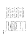
- Figs. 2 and 3 are drawings showing major steps in a method for fabricating the Group III nitride semiconductor device and the epitaxial substrate, according to the present embodiment.
- Figs. 4 and 5 are drawings schematically showing products in principal steps in the method for fabricating the Group III nitride semiconductor device and the epitaxial substrate, according to the present embodiment.
- the epitaxial substrate and the Group III nitride semiconductor optical device of the structure of a light emitting device are fabricated on a substrate by metal organic vapor phase epitaxy.
- Raw materials for epitaxial growth used herein are as follows: trimethylgallium (TMG), trimethylindium (TMI); trimethylaluminum (TMA); ammonia (NH 3 ); silane (SiH 4 ); and bis(cyclopentadienyl)magnesium (Cp 2 Mg).
- a substrate with a primary surface (substrate 51 shown in part (a) of Fig. 4 ) is prepared, which is made of a gallium nitride based semiconductor.
- a normal axis to the primary surface of the substrate 51 has an inclination angle in the angle range of 50 degrees to 130 degrees with respect to the c-axis of the gallium nitride based semiconductor.
- the substrate 51 has the primary surface inclined at the angle of 75 degrees from the c-plane toward the m-axis direction in hexagonal GaN, and this inclined surface is represented by ⁇ 20-21 ⁇ plane.
- the primary surface is mirror polished.
- step S102 Epitaxial growth is carried out under the below conditions on the substrate 51.
- the substrate 51 is loaded in a growth reactor 10.
- a quartz jig such as a quartz flow channel is placed.
- the substrate is the ally treated at the temperature of 1050 degrees Celsius and the in-reactor pressure of 27 kPa for ten minutes while supplying a thermal treatment gas containing NH 3 and H 2 into the growth reactor 10. This thermal treatment results in surface modification.
- step S103 Group III nitride semiconductor layers is grown on the substrate 51 to form the epitaxial substrate.
- step S104 a source gas containing raw materials for a Group III constituent element and a Group V constituent element, and an n-type dopant, and an atmosphere gas are supplied into the growth reactor 10 to epitaxially grow a Group III nitride semiconductor region 53.
- An inclination angle of a primary surface 53a of the Group III nitride semiconductor region 53 is associated with the inclination angle of the primary surface 51a of the substrate 51.
- the Group III nitride semiconductor region 53 can include one or more Group III nitride semiconductor layers.
- the atmosphere gas includes a carrier gas and a sub-flow gas.
- the atmosphere gas can contain, for example, nitrogen and/or hydrogen.
- the following gallium nitride based semiconductor region is grown.
- TMG, NH 3 , SiH 4 , and nitrogen and/or hydrogen are supplied into the growth reactor 10 to grow a Si-doped GaN layer 55a.
- TMG, TMI, TMA, NH 3 , SiH 4 , and nitrogen are supplied into the growth reactor 10 to grow a Si-doped InAlGaN layer 55b.
- TMG time to grow a Si-doped GaN layer 55c.
- NN 3 a Si-doped GaN layer 55c.
- nitrogen and/or hydrogen are supplied into the growth reactor 10 to grow a Si-doped GaN layer 55c.
- the hydrogen atmosphere of reducibility facilitates oxygen to desorb from the jig in the growth reactor and. deposits on this jig.
- step S105 a light emitting layer 57 is grown thereon.
- step S106 is carried out to supply TMG, TMI, NH 3 , and nitrogen into the growth reactor at the substrate temperature of 870 degrees Celsius to grow an InGaN optical guiding layer 59a.
- a part or the whole of the optical guiding layer 59a can be undoped or n-type conductive.
- step S107 is carried out to supply TMG, TMI, NH 3 , and atmosphere gas of nitrogen into the growth reactor to grow an undoped InGaN barrier layer 61a.
- the thickness of the InGaN layer 61a is 15 nm.
- semiconductor growth is interrupted and the substrate temperature is changed from the growth temperature of the barrier layer to the growth temperature of the well layer.
- step S108 TMG, TMI, NH 3 , and atmosphere gas of nitrogen supplied into the growth reactor 10 to grow an undoped InGaN well layer 61b.
- the thickness of the InGaN well layer 61 b can be 3 nm.
- the quantum well layer includes three well layers.
- step S109 TMG, TMI, NH 3 , and atmosphere gas of nitrogen is supplied into the growth reactor. 10 at the substrate temperature of 870 degrees Celsius to grow an InGaN, optical guiding layer 59c.
- a part or the whole of the optical guiding layer 59c can be undoped or p-type conductive.
- Inclination angles of primary surfaces of the light emitting layer 57 and active layer 59b are associated the inclination angle of the primary surface 51a of the substrate 51.
- Step S 110 is to supply a source gas containing a Group III raw material, a Group V raw material, and a p-type dopant, and an atmosphere gas into the growth reactor 10 to epitaxially grow a Group III nitride semiconductor region 63.
- An inclination angle of a primary surface 63a of the Group III nitride semiconductor region 63 corresponds to the inclination angle of the primary surface 51a of the substrate 51.
- the Group III nitride semiconductor region 63 can include one or more Group III nitride semiconductor layers.
- the gallium nitride based semiconductor region is grown, which will be described below.
- TMG the supply of TMG is terminated and then the substrate temperature is raised.
- TMG, NH 3 , Cp 2 Mg, and atmosphere gas are supplied into the growth reactor to grow a p-type GaN electron blocking layer 65a at the substrate temperature of 840 degrees Celsius.
- nitrogen it is preferable to supply nitrogen as atmosphere gas.
- TMG, TMI, NH 3 , Cp 2 Mg, and nitrogen are supplied into the growth reactor 10 to grow a Mg-doped InGaN optical guiding layer 65b at the substrate temperature of 840 degrees Celsius.
- TMG, NH 3 , Cp 2 Mg, and atmosphere gas are supplied into the growth reactor 10 to grow a Mg-doped GaN optical guiding layer 65c. In this growth, it is preferable to supply nitrogen as atmosphere gas.
- TMG, TMG, TMA, NH 3 , Cp 2 Mg, and nitrogen are supplied into the growth reactor 10 to grow a Mg-doped InAlGaN cladding layer 65d.
- TMG, NH 3 , Cp 2 Mg, and atmosphere gas are supplied into the growth reactor0 to grow a high-concentration Mg-doped GaN contact layer 65 e. In this growth, it is preferable to supply nitrogen as atmosphere gas.
- the epitaxial substrate EP1 is obtained.
- electrodes are formed on the epitaxial substrate EP1.
- the formation of electrodes is carried out as follows. For example, an electrode (Ni/Au) is formed on the p-type GaN contact layer 65e and an electrode (TilAl) is formed on a back surface of the epitaxial substrate EP1.
- a ridge structure can be formed by processing the epitaxial substrate EP1.
- the epitaxial growth of the p-type Group III nitride semiconductor region 63 in step S110 can be carried out in the below-described manner, as shown in Fig. 5 .
- the Group III nitride semiconductor region 63 can include one or more p-type gallium nitride based semiconductor layers containing indium as a Group III constituent element (which will be referred to as "p-type gallium nitride based semiconductor layer 63A"), and/or, one or more p-type gallium nitride based semiconductor layers not containing indium as a Group III constituent element (which will be referred to as "'p-type gallium nitride based semiconductor layer 63B").
- p-type gallium nitride based semiconductor layer 63A p-type gallium nitride based semiconductor layer 63A
- 'p-type gallium nitride based semiconductor layer 63B p-type gallium nitride based semiconductor layer 63B
- step S113 is a step of forming a partial layer 63C, which is a part of the p-type gallium nitride based semiconductor layer 63B, in a nitrogen atmosphere.
- an oxygen concentration of the p-type gallium nitride based semiconductor layer 63C becomes not more than 5 ⁇ 10 17 cm -3 and a ratio (Noxg/Npd) of the oxygen concentration Noxg to a p-type dopant concentration Npd of the p-type gallium nitride based semiconductor layer 63C becomes not more than 1/10.
- the subsequent step is carried out to form a remaining layer 63D, which is a part of the p-type gallium nitride based semiconductor layer 63B, in a hydrogen atmosphere.
- the arrangement of growth steps of the layers 63A, 63C, and 63D can be changed.
- a Group III nitride semiconductor region 65 can include one or more p-type gallium nitride based semiconductor layers containing indium as a Group III constituent element (which will be referred to as "p-type gallium nitride based semiconductor layers 65A"), and one or more p-type gallium nitride based semiconductor layers not containing indium as a Group III constituent element (which will be referred to as "p-type gallium nitride based semiconductor layers 65B").
- p-type gallium nitride based semiconductor layers 65A p-type gallium nitride based semiconductor layers 65A
- p-type gallium nitride based semiconductor layers 65B p-type gallium nitride based semiconductor layers 65B
- an oxygen concentration of the p-type gallium nitride based semiconductor layer 65A is made not more than 5 ⁇ 10 17 cm -3 and a ratio (Noxg/Npd) of the oxygen concentration Noxg to a p-type dopant concentration Npd of the p-type gallium nitride based semiconductor layer 65A is made not more than 1/10.
- the p-type gallium nitride based semiconductor layer 65B is formed in a nitrogen atmosphere.
- an oxygen concentration of the p-type gallium nitride based semiconductor layer 65B is made not more than 5 ⁇ 10 17 cm -3 and a ratio (Noxg/Npd) of the oxygen concentration Noxg to a p-type dopant concentration Npd of the p-type gallium nitride based semiconductor layer 65B is made not more than 1/10.
- the arrangement of growth steps of the layers 65A and 65B can be changed.
- a Group III nitride semiconductor region 67 can include one or more p-type gallium nitride based semiconductor layers containing indium as a Group III constituent element (which will be referred to as "p-type gallium nitride based semiconductor layers 67A”), one or more p-type gallium nitride based semiconductor layers not containing indium as a Group III constituent element (which will be referred to as "p-type gallium nitride based semiconductor layers 67B”), and a p-type contact layer 67C. As shown in part (f) of Fig.
- step S116 the whole of the p-type gallium nitride based semiconductor layers 67A is formed in a nitrogen atmosphere and the whole of the p-type gallium nitride based semiconductor layers 67B is formed in a nitrogen atmosphere.
- oxygen concentrations of these layers 67A, 67B are made not more than 5 ⁇ 10 17 cm -3 , and ratios (Noxg/Npd) of the oxygen concentrations Noxg to p-type dopant concentrations Npd of these layers 67A, 67B are made not more than 1/10.
- step S117 the p-type gallium nitride based semiconductor contact layer 67C is formed thereon.
- This contact layer 67C can also be formed in a nitrogen atmosphere and this growth can make an oxygen concentration of the contact layer 67C not more than 5 ⁇ 10 17 cm -3 .
- the source gas for the Group III and Group V constituent elements, and the atmosphere gas are supplied into the quartz tube of the growth reactor.
- the rate of the atmosphere gas (atmosphere gas/(atmosphere gas + source gas)) can be not less than 60%.
- the percentage herein is percent in volume. Examples in the present embodiment will be described below.
- a laser diode is fabricated in the device structure shown in part (a) of Fig. 6 .
- atmosphere gases are shown for respective constituent layers of an epitaxial structure.
- a ⁇ 20-21 ⁇ -plane GaN substrate is prepared.
- An epitaxial lamination is formed on this GaN substrate by metal organic vapor phase epitaxy.
- growth of p-type gallium nitride based semiconductor layers growth of each gallium nitride based semiconductor layer not containing indium (In) is carried out in a hydrogen atmosphere made with supply of only hydrogen as atmosphere gas. Growth of each gallium nitride based semiconductor layer containing indium (In) is carried out in a nitrogen atmosphere made with supply of only nitrogen as atmosphere gas.
- An insulating film (silicon oxide film) having a stripe window with the width of 10 ⁇ m is formed on the epitaxial lamination.
- a Pd electrode as an anode electrode is formed by evaporation. After this formation, a pad electrode is formed by evaporation.
- the substrate product obtained in this manner is separated at an interval of 600 ⁇ m to produce a laser bar.
- a reflecting film of a dielectric multilayer film is deposited on each of end faces for the optical cavity of the laser bar.
- the dielectric multilayer film comprises SiO 2 /TiO 2 .
- the reflectance of the front end face is made 80% and the reflectance of the rear end face is made 95%.
- the laser diode lases at the wavelength of 520 nm with the threshold current of 4 kA/cm 2 and its operating voltage is 8.5 V.
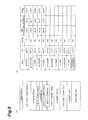
- magnesium concentration, oxygen concentration, and O/Mg ratio thereof are shown.
- "3e20" represents 3 ⁇ 10 20 .
- the gallium nitride based semiconductor layers containing indium (In), e.g., p-type InGaN and p-type InAlGaN are grown in the nitrogen atmosphere made with supply of only nitrogen as atmosphere gas, and the oxygen concentrations thereof are not more than 5 ⁇ 10 17 cm -3 .
- the O/Mg ratios are not more than 0.1.
- the V/III ratio of approximately 5000 to 10000 is used.
- the oxygen concentrations are high in the growth of the p-type gallium nitride based semiconductor layers formed with supply of only hydrogen as atmosphere gas (gallium nitride based semiconductor layers not containing indium (In)).
- a laser diode is fabricated in the device structure shown in part (a) of Fig. 7 .
- atmosphere gases are shown for respective constituent layers of an epitaxial structure.
- a ⁇ 20-21 ⁇ -plane GaN substrate is prepared.
- An epitaxial lamination is formed on this GaN substrate by metal organic vapor phase epitaxy.
- growth of p-type gallium nitride based semiconductor layers growth of each gallium nitride based semiconductor layer not containing indium (In) is carried out in an atmosphere formed with supply of nitrogen or hydrogen as atmosphere gas. Growth of each gallium nitride based semiconductor layer containing indium (In) is carried out in an atmosphere formed with supply of only nitrogen as atmosphere gas.
- the insulating film, anode electrode, etc. are produced on the epitaxial lamination to obtain a substrate product.
- This substrate product is separated at an interval of 600 ⁇ m to obtain laser bars.
- the reflecting film comprising the dielectric multilayer film is deposited on each of end faces for the optical cavity of the laser bar.
- the laser diode lases at the wavelength of 520 nm with the threshold current of 4 kA/cm 2 and its operating voltage is 8.0 V.
- the gallium nitride based semiconductor layers containing indium (In), e.g., p-type InGaN and p-type InAlGaN, are grown in the nitrogen atmosphere formed with supply of only nitrogen as atmosphere gas, and the O/Mg ratios are not more than 0.1. In the film formation condition thereof, the V/III ratio of approximately 5000 to 10000 is used.
- the oxygen concentration is low and the O/Mg ratio is not more than 0.1.
- the oxygen concentrations are high in the growth of the p-type GaN electron blocking layer and p+ GaN contact layer formed with supply of only hydrogen as atmosphere gas.
- a laser diode is fabricated in the device structure shown in part (a) of Fig. 8 .
- atmosphere gases are shown for respective constituent layers of an epitaxial structure.
- a ⁇ 20-21 ⁇ -plane GaN substrate is prepared.
- An epitaxial lamination is formed on this GaN substrate by metal organic vapor phase epitaxy.
- growth of p-type gallium nitride based semiconductor layers growth of each gallium nitride based semiconductor layer not containing indium (In) is carried out in an atmosphere formed with supply of nitrogen or hydrogen as atmosphere gas. Growth of each gallium nitride based semiconductor layer containing indium (In) is carried out in a nitrogen atmosphere formed with supply of only nitrogen as atmosphere gas.
- the insulating film, anode electrode, etc. are produced on the epitaxial lamination to obtain a substrate product.
- This substrate product is separated at an interval of 600 ⁇ m to obtain a laser bar.
- the reflecting film of the dielectric multilayer film is deposited on each of end faces for the optical cavity of the laser bar.
- the laser diode lases at the wavelength of 520 nm with the threshold current of 4 kA/cm 2 and its operating voltage is 7.5 V.
- the gallium nitride based semiconductor layers containing indium (In), e.g., p-type InGaN and p-type InAlGaN are grown in a nitrogen atmosphere formed with supply of only nitrogen as atmosphere gas, and the O/Mg ratios thereof are not more than 0.1.
- the gallium nitride based semiconductor layers not containing indium (In), e.g., the p-type GaN optical guiding layer and the p-type GaN electron blocking layer, are grown with supply of only nitrogen as atmosphere gas, whereas the other gallium nitride based semiconductor layer not containing indium (In), e.g., the p+ type GaN contact layer, is grown in a hydrogen atmosphere.
- the oxygen concentrations thereof are low and the O/Mg ratios are not more than 0.1.
- the V/III ratio of approximately 5000 to 10000 is used.
- the oxygen concentration is high in the growth of the p+ GaN contact layer formed with supply of only hydrogen as atmosphere gas.
- a laser diode is fabricated in the device structure shown in part (a) of Fig. 9 .
- atmosphere gases are shown for respective constituent layers of an epitaxial structure.
- a ⁇ 20-21 ⁇ -plane GaN substrate is prepared.
- An epitaxial lamination is formed on this GaN substrate by metal organic vapor phase epitaxy.
- growth of p-type gallium nitride based semiconductor layers growth of each gallium nitride based semiconductor layer not containing indium (In) is carried out in a nitrogen atmosphere formed with supply of only nitrogen as atmosphere gas. Growth of each gallium nitride based semiconductor layer containing indium (In) is carried out in a nitrogen atmosphere formed with supply of only nitrogen as atmosphere gas.
- the insulating film, anode electrode, etc. are produced on the epitaxial lamination to obtain a substrate product.
- This substrate product is separated at an interval of 600 ⁇ m to obtain a laser bar.
- the reflecting film comprised of the dielectric multilayer film is deposited on each of end faces for the optical cavity of the laser bar.
- the laser diode lases at the wavelength of 520 nm with the threshold current of 4 kA/cm 2 and its operating voltage is 7.0 V.
- the magnesium concentration, oxygen concentration, and O/Mg ratio thereof oxygen concentration/magnesium concentration
- the V/III ratio of approximately 5000 to 10000 is used.
- the gallium nitride based semiconductor layers not containing indium (In), e.g., the p-type GaN optical guiding layer, the p-type GaN electron blocking layer, and the p+ GaN contact layer, are formed with supply of only nitrogen as atmosphere gas, and thus the growth of all the p-type gallium nitride based semiconductor layers is carried out in the nitrogen atmosphere.
- the oxygen concentrations are made low and the O/Mg ratios made are not more than 0.1 in the growth of the p-type GaN optical guiding layer, p-type GaN electron blocking layer, and p+ GaN contact layer formed with supply of only nitrogen as atmosphere gas.
- a laser diode is fabricated in the device structure shown in part (a) of Fig. 10 .
- atmosphere gases are shown for respective constituent layers of an epitaxial structure.
- a ⁇ 20-21 ⁇ -plane GaN substrate is prepared.
- An epitaxial lamination is formed on this GaN substrate by metal organic vapor phase epitaxy.
- the growth of the gallium nitride based semiconductor layers not containing indium (In) and the growth of the gallium nitride based semiconductor layers containing indium (In) are carried out in a nitrogen atmosphere formed with supply of only nitrogen as atmosphere gas.
- the surface roughness of the epitaxial substrate is not more than 1 nm in arithmetic average roughness.
- Example 2 In the same manner as in Example 1, the insulating film, anode electrode, etc. are produced on the epitaxial lamination to obtain a substrate product. This substrate product is separated at an interval of 600 ⁇ m to obtain a laser bar.
- the reflecting film comprised of the dielectric multilayer film is deposited on each of end faces for the optical cavity of the laser bar. The laser diode lases at the wavelength of 520 nm with the threshold current of 4 kA/cm 2 and its operating voltage is 6.5 V.
- the p-type and n-type gallium nitride based semiconductor layers are grown with supply of only nitrogen as atmosphere gas.
- the oxygen concentrations are low, and the O/Mg ratios are not more than 0.1 in the growth of the gallium nitride based semiconductor layers formed with supply of only nitrogen as atmosphere gas.
- the technical contributions as described below are also achieved in addition to the reduction of driving voltage.
- the number of switching of carrier gas is reduced, so as to reduce dusts such as particles produced during the growth.
- impurities decrease at interfaces.
- the nitrogen carrier gas is used, the epitaxial surfaces become flattened, so as to improve the surface morphology. This improves the chip yield and device reliability.
- the O/Mg ratio is not more than 0.1 in the growth of a p-type gallium nitride based semiconductor layer(s), which is grown in the nitrogen atmosphere formed with supply of only nitrogen as atmosphere gas, among the p-type gallium nitride based semiconductor layers.
- the inventors carry out a number of trials to reduce the oxygen concentration, such as selection of high-purity raw materials, cleaning of the substrate before the epitaxial growth, and cleaning of the jig, but any of them has achieved no satisfactory effect.
- the semipolar plane demonstrates incorporation of oxygen about one figure higher than the c-plane. For this reason, incorporation of oxygen impurity in the growth onto the c-plane does not significantly affect the quality of the epitaxially grown film. However, it can be a cause to degrade, particularly, the electrical characteristics of the p-type semiconductor layers, in the growth onto the semipolar plane.
- the inventors have discovered, on the way of experiments for improvement as described above, that the gallium nitride based semiconductor layer containing In is grown in the nitrogen atmosphere and the oxygen concentration of this gallium nitride based semiconductor layer is lower than those of the other layers not containing In grown in the hydrogen atmosphere. Therefore, when the gallium nitride based semiconductor layer not containing In is grown in the nitrogen atmosphere, the oxygen concentration of this gallium nitride based semiconductor layer can reduce. This can lower the internal resistance of the semiconductor device. It is verified by experiment that the oxygen concentration of the gallium nitride based semiconductor layer grown in the nitrogen atmosphere can be reduced and a low-resistance semiconductor device can be fabricated.
- the oxygen supply sources are considered to be such supply sources as impurities contained in the gas, such as the raw materials supplied the growth reactor, and the jig other than them.
- the impurities in the raw materials are oxygen supply sources, conceivable factors include “oxygen concentrations in the raw materials” and “incorporation coefficient of oxygen into crystal.”
- the oxygen concentration increases in the epitaxial semiconductor crystal in either of the hydrogen atmosphere or the nitrogen atmosphere in film formation with lowered purity of the source gas. From this result, the "incorporation coefficient of oxygen into crystal" is considered to be independent of the atmosphere gas.
- oxygen sources are other than the raw materials
- conceivable factors include “oxygen sources” such as the jig in the reactor, deposits, and residue of cleaner, "desorption coefficient of oxygen from oxygen sources,” and “incorporation coefficient of oxygen into crystal.”
- oxygen sources such as the jig in the reactor, deposits, and residue of cleaner
- desorption coefficient of oxygen from oxygen sources and "incorporation coefficient of oxygen into crystal.”
- the "incorporation coefficient of oxygen into crystal” is independent of the atmosphere gas. Therefore, the rest “incorporation coefficient of oxygen into crystal” varies depending upon the atmosphere gas. Hydrogen works as reducing gas and makes oxygen desorbed from unwanted deposited materials such as deposits. It is considered that this oxygen is incorporated into the epitaxial crystal. For this reason, it is preferable to use nitrogen as atmosphere gas (carrier gas and sub-flow gas).
- the present embodiment according to the present invention can provide a Group III nitride semiconductor device having a p-type gallium nitride based semiconductor layer with a reduced oxygen concentration. Further, the present embodiment according to the present invention can provide a method for fabricating the Group III nitride semiconductor device, which can reduce an incorporation amount of oxygen impurity. Furthermore, the present embodiment according to the present invention can provide an epitaxial substrate for the Group III nitride semiconductor device.
Landscapes
- Physics & Mathematics (AREA)
- Optics & Photonics (AREA)
- Engineering & Computer Science (AREA)
- Condensed Matter Physics & Semiconductors (AREA)
- General Physics & Mathematics (AREA)
- Electromagnetism (AREA)
- Nanotechnology (AREA)
- Chemical & Material Sciences (AREA)
- Biophysics (AREA)
- Crystallography & Structural Chemistry (AREA)
- Life Sciences & Earth Sciences (AREA)
- Led Devices (AREA)
- Semiconductor Lasers (AREA)
Applications Claiming Priority (2)
| Application Number | Priority Date | Filing Date | Title |
|---|---|---|---|
| JP2010248932A JP5842324B2 (ja) | 2010-11-05 | 2010-11-05 | Iii族窒化物半導体素子、iii族窒化物半導体素子を作製する方法、及びエピタキシャル基板 |
| PCT/JP2011/074973 WO2012060299A1 (ja) | 2010-11-05 | 2011-10-28 | Iii族窒化物半導体素子、iii族窒化物半導体素子を作製する方法、及びエピタキシャル基板 |
Publications (1)
| Publication Number | Publication Date |
|---|---|
| EP2637267A1 true EP2637267A1 (en) | 2013-09-11 |
Family
ID=46018759
Family Applications (1)
| Application Number | Title | Priority Date | Filing Date |
|---|---|---|---|
| EP11837949.4A Withdrawn EP2637267A1 (en) | 2010-11-05 | 2011-10-28 | Group iii nitride semiconductor device, method of manufacturing group iii nitride semiconductor devices, and epitaxial substrate |
Country Status (6)
| Country | Link |
|---|---|
| US (1) | US8809868B2 (enExample) |
| EP (1) | EP2637267A1 (enExample) |
| JP (1) | JP5842324B2 (enExample) |
| CN (1) | CN103190042A (enExample) |
| TW (1) | TW201234415A (enExample) |
| WO (1) | WO2012060299A1 (enExample) |
Families Citing this family (15)
| Publication number | Priority date | Publication date | Assignee | Title |
|---|---|---|---|---|
| JP2821900B2 (ja) | 1989-04-05 | 1998-11-05 | 日本鉄道建設公団 | 音波制御装置を配置した輸送用高架構造物 |
| JP2820770B2 (ja) | 1990-04-19 | 1998-11-05 | 株式会社ブリヂストン | 干渉型防音装置 |
| JP5387302B2 (ja) * | 2009-09-30 | 2014-01-15 | 住友電気工業株式会社 | Iii族窒化物半導体レーザ素子、及びiii族窒化物半導体レーザ素子を作製する方法 |
| KR101659738B1 (ko) * | 2010-07-08 | 2016-09-26 | 엘지이노텍 주식회사 | 발광 소자 제조방법 |
| JP5361925B2 (ja) * | 2011-03-08 | 2013-12-04 | 株式会社東芝 | 半導体発光素子およびその製造方法 |
| JP6176141B2 (ja) * | 2014-02-19 | 2017-08-09 | 豊田合成株式会社 | Iii 族窒化物半導体発光素子の製造方法 |
| TWI577046B (zh) * | 2014-12-23 | 2017-04-01 | 錼創科技股份有限公司 | 半導體發光元件及其製作方法 |
| CN111052414B (zh) * | 2017-08-24 | 2023-07-21 | 日本碍子株式会社 | 13族元素氮化物层、自立基板以及功能元件 |
| US10665750B2 (en) | 2017-11-22 | 2020-05-26 | Epistar Corporation | Semiconductor device |
| CN110838514B (zh) * | 2018-08-17 | 2022-07-22 | 苏州能讯高能半导体有限公司 | 一种半导体器件的外延结构及其制备方法、半导体器件 |
| JP6744521B1 (ja) * | 2018-12-11 | 2020-08-19 | パナソニックセミコンダクターソリューションズ株式会社 | 窒化物系半導体発光素子及びその製造方法、並びに、窒化物系半導体結晶の製造方法 |
| JP7422496B2 (ja) * | 2019-06-21 | 2024-01-26 | 古河機械金属株式会社 | 構造体、光デバイス、光デバイスの製造方法、構造体の製造方法 |
| US11527701B2 (en) * | 2019-10-28 | 2022-12-13 | Taiwan Semiconductor Manufacturing Company, Ltd. | Piezoelectric device and method of forming the same |
| JP7269190B2 (ja) * | 2020-02-27 | 2023-05-08 | 株式会社東芝 | 窒化物結晶、光学装置、半導体装置、窒化物結晶の製造方法 |
| WO2022068256A1 (zh) * | 2020-09-30 | 2022-04-07 | 苏州能讯高能半导体有限公司 | 半导体器件的外延结构及其制备方法 |
Family Cites Families (10)
| Publication number | Priority date | Publication date | Assignee | Title |
|---|---|---|---|---|
| JP2751987B2 (ja) | 1992-11-20 | 1998-05-18 | 日亜化学工業株式会社 | 窒化インジウムガリウム半導体の成長方法 |
| JP2005191530A (ja) * | 2003-12-03 | 2005-07-14 | Sumitomo Electric Ind Ltd | 発光装置 |
| JP4121985B2 (ja) * | 2004-07-16 | 2008-07-23 | 昭和電工株式会社 | GaN系化合物半導体の製造方法 |
| JP5053362B2 (ja) * | 2007-03-23 | 2012-10-17 | 株式会社トクヤマ | P型iii族窒化物半導体およびiii族窒化物半導体素子 |
| CN101689586B (zh) * | 2007-06-15 | 2012-09-26 | 罗姆股份有限公司 | 氮化物半导体发光元件和氮化物半导体的制造方法 |
| JP5077303B2 (ja) * | 2008-10-07 | 2012-11-21 | 住友電気工業株式会社 | 窒化ガリウム系半導体発光素子、窒化ガリウム系半導体発光素子を作製する方法、窒化ガリウム系発光ダイオード、エピタキシャルウエハ、及び窒化ガリウム系発光ダイオードを作製する方法 |
| JP5316276B2 (ja) * | 2009-01-23 | 2013-10-16 | 住友電気工業株式会社 | 窒化物半導体発光素子、エピタキシャル基板、及び窒化物半導体発光素子を作製する方法 |
| JP5529420B2 (ja) * | 2009-02-09 | 2014-06-25 | 住友電気工業株式会社 | エピタキシャルウエハ、窒化ガリウム系半導体デバイスを作製する方法、窒化ガリウム系半導体デバイス、及び酸化ガリウムウエハ |
| JP5316359B2 (ja) * | 2009-02-20 | 2013-10-16 | 住友電気工業株式会社 | 窒化ガリウム系半導体電子デバイスを作製する方法、エピタキシャル基板、及び窒化ガリウム系半導体電子デバイス |
| JP2010212651A (ja) * | 2009-09-08 | 2010-09-24 | Sumitomo Electric Ind Ltd | Iii族窒化物半導体素子、エピタキシャル基板、及びiii族窒化物半導体素子を作製する方法 |
-
2010
- 2010-11-05 JP JP2010248932A patent/JP5842324B2/ja not_active Expired - Fee Related
-
2011
- 2011-10-28 CN CN2011800534287A patent/CN103190042A/zh active Pending
- 2011-10-28 EP EP11837949.4A patent/EP2637267A1/en not_active Withdrawn
- 2011-10-28 WO PCT/JP2011/074973 patent/WO2012060299A1/ja not_active Ceased
- 2011-11-04 TW TW100140401A patent/TW201234415A/zh unknown
- 2011-11-04 US US13/289,813 patent/US8809868B2/en active Active
Non-Patent Citations (1)
| Title |
|---|
| See references of WO2012060299A1 * |
Also Published As
| Publication number | Publication date |
|---|---|
| WO2012060299A1 (ja) | 2012-05-10 |
| US8809868B2 (en) | 2014-08-19 |
| CN103190042A (zh) | 2013-07-03 |
| JP2012104515A (ja) | 2012-05-31 |
| US20120112203A1 (en) | 2012-05-10 |
| JP5842324B2 (ja) | 2016-01-13 |
| TW201234415A (en) | 2012-08-16 |
Similar Documents
| Publication | Publication Date | Title |
|---|---|---|
| US8809868B2 (en) | Group-III nitride semiconductor device, method for fabricating Group-III nitride semiconductor device, and epitaxial substrate | |
| CN101919076B (zh) | Ⅲ族氮化物半导体器件、外延衬底及ⅲ族氮化物半导体器件的制作方法 | |
| JP5381439B2 (ja) | Iii族窒化物半導体光素子 | |
| EP2144306A1 (en) | Group III nitride semiconductor light-emitting device and epitaxial wafer | |
| US8344413B2 (en) | Nitride semiconductor wafer, nitride semiconductor chip, and method of manufacture of nitride semiconductor chip | |
| US20110001126A1 (en) | Nitride semiconductor chip, method of fabrication thereof, and semiconductor device | |
| EP2728683A1 (en) | Group iii nitride semiconductor element and method for manufacturing group iii nitride semiconductor element | |
| US20110042646A1 (en) | Nitride semiconductor wafer, nitride semiconductor chip, method of manufacture thereof, and semiconductor device | |
| CN102292884A (zh) | 氮化物半导体发光元件、外延基板及氮化物半导体发光元件的制作方法 | |
| US6462354B1 (en) | Semiconductor device and semiconductor light emitting device | |
| KR20100099066A (ko) | 질화갈륨계 반도체 광소자, 질화갈륨계 반도체 광소자를 제조하는 방법 및 에피택셜 웨이퍼 | |
| CN102422497B (zh) | Iii族氮化物半导体激光二极管及iii族氮化物半导体激光二极管的制作方法 | |
| CN103377915A (zh) | 氮化镓系半导体的制造方法、iii族氮化物半导体器件及其制造方法 | |
| JP5651077B2 (ja) | 窒化ガリウム系半導体レーザ素子、及び、窒化ガリウム系半導体レーザ素子の製造方法 | |
| JP5310382B2 (ja) | Iii族窒化物半導体光素子、及びiii族窒化物半導体光素子を作製する方法 | |
| JP2000349398A (ja) | 窒化物半導体発光素子及びその製造方法 | |
| JP2010212651A (ja) | Iii族窒化物半導体素子、エピタキシャル基板、及びiii族窒化物半導体素子を作製する方法 |
Legal Events
| Date | Code | Title | Description |
|---|---|---|---|
| PUAI | Public reference made under article 153(3) epc to a published international application that has entered the european phase |
Free format text: ORIGINAL CODE: 0009012 |
|
| 17P | Request for examination filed |
Effective date: 20130605 |
|
| AK | Designated contracting states |
Kind code of ref document: A1 Designated state(s): AL AT BE BG CH CY CZ DE DK EE ES FI FR GB GR HR HU IE IS IT LI LT LU LV MC MK MT NL NO PL PT RO RS SE SI SK SM TR |
|
| DAX | Request for extension of the european patent (deleted) | ||
| STAA | Information on the status of an ep patent application or granted ep patent |
Free format text: STATUS: THE APPLICATION HAS BEEN WITHDRAWN |
|
| 18W | Application withdrawn |
Effective date: 20150312 |