WO2012026074A1 - Dispositif et module de capture d'image et appareil photographique - Google Patents
Dispositif et module de capture d'image et appareil photographique Download PDFInfo
- Publication number
- WO2012026074A1 WO2012026074A1 PCT/JP2011/004452 JP2011004452W WO2012026074A1 WO 2012026074 A1 WO2012026074 A1 WO 2012026074A1 JP 2011004452 W JP2011004452 W JP 2011004452W WO 2012026074 A1 WO2012026074 A1 WO 2012026074A1
- Authority
- WO
- WIPO (PCT)
- Prior art keywords
- image pickup
- area
- semiconductor substrate
- thickness
- pickup device
- Prior art date
Links
- 239000000758 substrate Substances 0.000 claims abstract description 131
- 239000004065 semiconductor Substances 0.000 claims abstract description 105
- 230000000149 penetrating effect Effects 0.000 claims abstract description 21
- XUIMIQQOPSSXEZ-UHFFFAOYSA-N Silicon Chemical compound [Si] XUIMIQQOPSSXEZ-UHFFFAOYSA-N 0.000 claims description 26
- 229910052710 silicon Inorganic materials 0.000 claims description 26
- 239000010703 silicon Substances 0.000 claims description 26
- 239000011521 glass Substances 0.000 claims description 7
- 230000003287 optical effect Effects 0.000 claims description 7
- 230000014509 gene expression Effects 0.000 claims description 5
- 239000004033 plastic Substances 0.000 claims description 3
- 239000010408 film Substances 0.000 description 12
- 239000012789 electroconductive film Substances 0.000 description 10
- 238000005336 cracking Methods 0.000 description 9
- 230000001747 exhibiting effect Effects 0.000 description 6
- 238000005476 soldering Methods 0.000 description 6
- 229920005989 resin Polymers 0.000 description 5
- 239000011347 resin Substances 0.000 description 5
- 239000000853 adhesive Substances 0.000 description 4
- 230000001070 adhesive effect Effects 0.000 description 4
- 230000004048 modification Effects 0.000 description 4
- 238000012986 modification Methods 0.000 description 4
- 239000011229 interlayer Substances 0.000 description 3
- 229910000679 solder Inorganic materials 0.000 description 3
- 230000001413 cellular effect Effects 0.000 description 2
- 238000010586 diagram Methods 0.000 description 2
- 238000004519 manufacturing process Methods 0.000 description 2
- 230000009467 reduction Effects 0.000 description 2
- RZVAJINKPMORJF-UHFFFAOYSA-N Acetaminophen Chemical compound CC(=O)NC1=CC=C(O)C=C1 RZVAJINKPMORJF-UHFFFAOYSA-N 0.000 description 1
- 230000008901 benefit Effects 0.000 description 1
- 239000005352 borofloat Substances 0.000 description 1
- 239000000919 ceramic Substances 0.000 description 1
- 238000006243 chemical reaction Methods 0.000 description 1
- 239000003795 chemical substances by application Substances 0.000 description 1
- 230000003247 decreasing effect Effects 0.000 description 1
- 230000006870 function Effects 0.000 description 1
- 239000000463 material Substances 0.000 description 1
- 238000004806 packaging method and process Methods 0.000 description 1
- 230000002093 peripheral effect Effects 0.000 description 1
- 229920005668 polycarbonate resin Polymers 0.000 description 1
- 239000004431 polycarbonate resin Substances 0.000 description 1
- 239000005297 pyrex Substances 0.000 description 1
- 230000011514 reflex Effects 0.000 description 1
- 239000000523 sample Substances 0.000 description 1
Images


Classifications
-
- H—ELECTRICITY
- H01—ELECTRIC ELEMENTS
- H01L—SEMICONDUCTOR DEVICES NOT COVERED BY CLASS H10
- H01L27/00—Devices consisting of a plurality of semiconductor or other solid-state components formed in or on a common substrate
- H01L27/14—Devices consisting of a plurality of semiconductor or other solid-state components formed in or on a common substrate including semiconductor components sensitive to infrared radiation, light, electromagnetic radiation of shorter wavelength or corpuscular radiation and specially adapted either for the conversion of the energy of such radiation into electrical energy or for the control of electrical energy by such radiation
- H01L27/144—Devices controlled by radiation
- H01L27/146—Imager structures
- H01L27/14601—Structural or functional details thereof
- H01L27/14618—Containers
-
- H—ELECTRICITY
- H04—ELECTRIC COMMUNICATION TECHNIQUE
- H04N—PICTORIAL COMMUNICATION, e.g. TELEVISION
- H04N25/00—Circuitry of solid-state image sensors [SSIS]; Control thereof
-
- H—ELECTRICITY
- H01—ELECTRIC ELEMENTS
- H01L—SEMICONDUCTOR DEVICES NOT COVERED BY CLASS H10
- H01L23/00—Details of semiconductor or other solid state devices
- H01L23/28—Encapsulations, e.g. encapsulating layers, coatings, e.g. for protection
- H01L23/31—Encapsulations, e.g. encapsulating layers, coatings, e.g. for protection characterised by the arrangement or shape
- H01L23/3107—Encapsulations, e.g. encapsulating layers, coatings, e.g. for protection characterised by the arrangement or shape the device being completely enclosed
- H01L23/3121—Encapsulations, e.g. encapsulating layers, coatings, e.g. for protection characterised by the arrangement or shape the device being completely enclosed a substrate forming part of the encapsulation
- H01L23/3128—Encapsulations, e.g. encapsulating layers, coatings, e.g. for protection characterised by the arrangement or shape the device being completely enclosed a substrate forming part of the encapsulation the substrate having spherical bumps for external connection
-
- H—ELECTRICITY
- H01—ELECTRIC ELEMENTS
- H01L—SEMICONDUCTOR DEVICES NOT COVERED BY CLASS H10
- H01L2924/00—Indexing scheme for arrangements or methods for connecting or disconnecting semiconductor or solid-state bodies as covered by H01L24/00
- H01L2924/0001—Technical content checked by a classifier
- H01L2924/0002—Not covered by any one of groups H01L24/00, H01L24/00 and H01L2224/00
Definitions
- the present invention relates to an image pickup device, an image pickup module, and a camera.
- a wafer-level chip size packaging (WL-CSP) technology in which a semiconductor substrate, which includes an image pickup element and a penetrating electrode, and a light-transmission support substrate are fixed together using an adhesive so as to form a space above the image pickup element is known as a technology used for image pickup devices (see PTL 1 and PTL 2).
- a technology used for image pickup devices see PTL 1 and PTL 2.
- the image pickup devices disclosed in PTL 1 and PTL 2 have a configuration in which the thickness of a semiconductor substrate below a space when viewed from a light-transmission support substrate is greater than the thickness of the semiconductor substrate below an adhesive.
- Small-sized image pickup devices are used for cellular phones. Reductions in size and thickness are also required for image pickup devices of a larger size, such as single-lens reflex cameras.
- the present invention provides an image pickup device and an image pickup system that exhibit a high reliability and for which there is a reduced possibility of deformation and cracking of a semiconductor substrate.
- An image pickup device includes a transparent member, an image pickup element chip including a photodiode, and a fixing member that is arranged around the image pickup element chip, a space being surrounded by the transparent member, the image pickup element chip, and the fixing member.
- the image pickup element chip includes a semiconductor substrate, and the semiconductor substrate includes a penetrating electrode that penetrates through a first main face of the semiconductor substrate on a side of the transparent member and a second main face of the semiconductor substrate opposite the first main face.
- the penetrating electrode is arranged in a fixing area corresponding to the fixing member, and a boundary with an area in which the thickness of the semiconductor substrate is smaller than the thickness of the semiconductor substrate in a first area corresponding to the space is arranged within the fixing area.
- an image pickup device and an image pickup system that exhibit a high reliability and for which there is a reduced possibility of deformation and cracking of a semiconductor substrate can be provided.
- Fig. 1 is an exploded perspective view of an image pickup device according to a first embodiment.
- Fig. 2A is a plan view of the image pickup device according to the first embodiment.
- Fig. 2B is a front view of the image pickup device according to the first embodiment.
- Fig. 3 includes a plan view and a sectional view of part of the image pickup device according to the first embodiment.
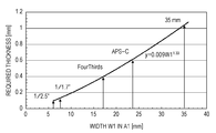
- Fig. 4 is a graph illustrating the thickness of a semiconductor substrate required when the longitudinal width W1 of the semiconductor substrate in a space portion of the image pickup device according to the first embodiment is changed.
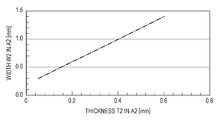
- Fig. 5 is a graph illustrating the thickness of the semiconductor substrate required when the thickness T2 of the semiconductor substrate in a second area of the image pickup device according to the first embodiment is changed.
- Fig. 1 is an exploded perspective view of an image pickup device according to a first embodiment.
- Fig. 2A is a plan view of the image pickup device according to the first embodiment.
- Fig. 2B is a front view of the image
- Fig. 6 includes a plan view and a sectional view of part of an image pickup device according to a second embodiment.
- Fig. 7 includes a plan view and a sectional view of part of an image pickup device according to a third embodiment.
- Fig. 8 illustrates an example of a case where an image pickup device is applied to an image pickup module to be used in a portable apparatus.
- Fig. 9 is a block diagram illustrating a case where an image pickup device is applied to a digital camera, which is an example of an image pickup system.
- Fig. 1 is an exploded perspective view of an image pickup device according to a first embodiment.
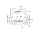
- the image pickup device includes a transparent member 1, an image pickup element chip 2, and a fixing member 3 arranged between the transparent member 1 and the image pickup element chip 2.
- the transparent member 1 is optically transparent and is made of glass, resin, or the like.
- a semiconductor substrate used for the image pickup element chip 2 is made of silicon
- the glass used for the transparent member 1 be BOROFLOAT (registered trademark) manufactured by SCHOTT AG, PYREX (registered trademark) manufactured by Corning Incorporated, an SW glass substrate manufactured by ASAHI GLASS CO., LTD, or the like.
- the resin used for the transparent member 1 may be made of optical plastic formed of a polycarbonate resin or the like.
- Such a transparent member made of glass or resin is a desirable material since glass and resin each have a coefficient of linear expansion close to that of silicon.
- a silicon substrate is used for the image pickup element chip 2.
- a microlens be arranged on a light incident side of the image pickup element chip 2.
- an adhesive is used for the fixing member 3.
- the fixing member 3 may be made of an organic resin or the like.
- the adhesive is formed, for example, by being patterned, on at least one of a surface of the transparent member 1 and a surface of the image pickup element chip 2.
- Fig. 2A is a plan view of the image pickup device according to the first embodiment.
- Fig. 2B is a front view of the image pickup device according to the first embodiment.
- the transparent member 1 and the image pickup element chip 2 are fixed to each other by the fixing member 3.
- a space 4 is formed by being surrounded by the transparent member 1, the image pickup element chip 2, and the fixing member 3.
- the image pickup element chip 2 includes a semiconductor substrate 11, a wiring structure 12 formed on the semiconductor substrate 11, and a microlens 13.
- the semiconductor substrate 11 is made of a silicon substrate.
- the image pickup element chip 2 also includes an insulating member 14 and a soldering ball 15 below the semiconductor substrate 11 (on a side opposite a light incident side of the semiconductor substrate 11).
- the image pickup element chip 2 also includes a penetrating electrode 16 that penetrates through a first main face on a side of the transparent member 1, which is a light incident side of the semiconductor substrate 11, and a second main face that is opposite the first main face.
- the penetrating electrode 16 is electrically connected to an internal electrode 17 arranged within the wiring structure 12.
- the penetrating electrode 16 includes an electroconductive film 18 and thus is electrically connected to the soldering ball 15.
- a planarizing film and a color filter, which are not illustrated, are arranged between the wiring structure 12 and the microlens 13. In a case where the image pickup device is viewed from the light incident side, that is, the image pickup device is viewed from the front side as illustrated in Fig.
- an area in which the fixing member 3 is arranged is defined as a fixing area, which corresponds to an area more outward than an inner circumference 19 of the fixing member 3.
- An area more inward than the inner circumference 19 is defined as a capturing area.
- the capturing area contains an area in which the microlens 13 of the image pickup element chip 2 is arranged, that is, a pixel area in which a photodiode for converting incident light into electric charge is arranged.
- An electrode portion including the internal electrode 17, the penetrating electrode 16, and the like of the image pickup element chip 2 is arranged in the fixing area.
- Fig. 2B also serves as an orthogonal projection that is orthogonal with respect to the configuration of part of the transparent member 1.
- Areas of the semiconductor substrate 11 have different thicknesses.
- a boundary 20 across which the thickness of the semiconductor substrate 11 changes is located below the fixing member 3, that is, within the area of the fixing area when viewed from the light incident side.
- the boundary across which the thickness of the semiconductor substrate 11 changes may correspond to the boundary of the fixing area in the orthogonal projection that is orthogonal with respect to the transparent member 1, it is desirable that the boundary across which the thickness of the semiconductor substrate 11 changes be located within the area of the fixing area.
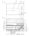
- Part A and part B of Fig. 3 are a partial plan view and a partial sectional view of the image pickup device taken along line IIIB-IIIB of Fig. 2A.
- the transparent member 1 and the image pickup element chip 2 are fixed to each other by the fixing member 3, which is arranged between the transparent member 1 and the image pickup element chip 2.
- the space 4 is formed by being surrounded by a surface of the image pickup element chip 2, the transparent member 1, and the fixing member 3.
- the image pickup device when viewed from the light incident side is categorized into a first area A1, which is a capturing area, a second area A2, which is part of a fixing area outside the first area A1, and a third area A3, which is part of the fixing area, located outside the second area A2, and is an electrode area in which a penetrating electrode is arranged.
- the first, second, and third areas A1 A2, and A3 have longitudinal widths of W1, W2, and W3, respectively.
- the first area A1 includes a pixel area 21 including a photodiode and a transistor for transferring a signal corresponding to electric charge obtained by photoelectric conversion by the photodiode, which are not illustrated.
- the wiring structure 12 including wiring and an inter-layer insulating film, which are not illustrated, is arranged on the first main face, which is on the light incident side of the semiconductor substrate 11.
- a first planarizing film 22 is arranged on the wiring structure 12.
- a color filter 23 is arranged on the first planarizing film 22.
- a second planarizing film 24 is arranged on the color filter 23.
- the microlens 13 is arranged on the second planarizing film 24.
- a through hole is formed through the semiconductor substrate 11 so as to extend from the first main face to the second main face of the semiconductor substrate 11, so that the penetrating electrode 16 is arranged.
- An insulating film 25 is arranged on the second main face of the semiconductor substrate 11 in which the through hole is arranged.
- the electroconductive film 18 is formed on the insulating film 25.
- a solder resist 26, which serves as a protection film, is arranged on the electroconductive film 18.
- An opening is formed in part of the solder resist 26 on the electroconductive film 18.
- the soldering ball 15 is arranged in the opening portion of the solder resist 26 on the electroconductive film 18.
- the transistor in the first area A1, a peripheral circuit, which is not illustrated, and the like are electrically connected to the electroconductive film 18 with the internal electrode 17 arranged in the wiring structure 12 therebetween.
- the penetrating electrode 16 includes the electroconductive film 18.
- the electroconductive film 18 may extend so as to reach a lower portion of the soldering ball 15.
- An element face electrode 27 is arranged on the internal electrode 17 with the inter-layer insulating film therebetween.
- a contact plug, which is not illustrated, for electrically connecting the internal electrode 17 to the element face electrode 27 is arranged in the inter-layer insulating film between the internal electrode 17 and the element face electrode 27.
- the element face electrode 27 is used for application of voltage, reading of a signal, and the like, via the contact plug and the internal electrode 17. In particular, when a die sort test is performed, a probe is applied to the element face electrode 27. And the boundary 20 with the third area A3 in which the thickness of the semiconductor substrate is smaller than the thickness of the semiconductor substrate in the first area A1 is arranged within the fixing area.
- Fig. 4 is a graph illustrating the thickness of the semiconductor substrate 11 required when the longitudinal width W1 of the space 4 is changed.
- the required thicknesses T1 and T2 of the semiconductor substrate 11 in the first area A1 and the second area A2 can be obtained using expression (1):
- the required thicknesses T1 and T2 of the semiconductor substrate 11 in the first area A1 and the second area A2 are summarized as described below.
- the size of the image pickup element chip 2 corresponds to the size of a 1/2.5-inch chip
- 0.1 mm or more is required.
- the size of the image pickup element chip 2 corresponds to the size of a Four Thirds chip
- 0.4 mm or more is required.
- the size of the image pickup element chip 2 corresponds to the size of an APS-C chip
- 0.6 mm or more is required.
- An image pickup element chip having a size corresponding to the size of a Four Thirds chip includes a pixel area of approximately 17.3 x 13 mm.
- An image pickup element chip having a size corresponding to the size of an APS-C chip includes a field angle of approximately 24.0 x 16 mm.
- Fig. 5 is a graph illustrating the width W2 required when the thickness T2 of the semiconductor substrate 11 in the second area A2 is changed.
- the width W2 required when the thickness T2 of the semiconductor substrate 11 in the second area A2 is changed can be obtained when expression (2) and (3) are consistent with each other.
- the thickness T3 of the semiconductor substrate 11 in the third area A3 satisfy expression (4): In order to improve the throughput in the step of forming the penetrating electrode and to achieve an excellent quality of the insulating film and the electroconductive film formed in the through hole, it is desirable that the thickness T3 of the semiconductor substrate 11 in the third area A3 be 0.2 mm or less.
- the required thickness T2 and width W2 of the semiconductor substrate 11 in the second area A2 are summarized as described below.
- the thickness T2 is required to be 0.1 mm or more and the width W2 is required to be 0.4 mm or more.
- the thickness T2 is required to be 0.4 mm or more and the width W2 is required to be 1.0 mm or more.
- the thickness T2 is required to be 0.6 mm or more and the width W2 is required to be 1.4 mm or more.
- each of the thicknesses T1, T2, and T3 corresponds to the distance between the second main face and the flat first main face of the semiconductor substrate 11 or a surface of the transparent member 1 on a side of the semiconductor substrate 11.
- the second main face of the semiconductor substrate 11 includes a recessed portion, that is, a thin portion, within the fixing area.
- an image pickup device exhibiting a high reliability can be achieved. Furthermore, when the thickness T2 and the width W2 of the second area A2 and the thickness T3 of the third area A3 satisfy the relationships described above, the possibility of cracking and deformation of the semiconductor substrate 11 can be reduced, thus achieving an image pickup device exhibiting a high reliability.
- a portion to be connected to the soldering ball 15 or the like may correspond to the boundary of the fixing area or be arranged within the fixing area in the orthogonal projection that is orthogonal with respect to the transparent member 1. Consequently, the possibility of deformation and cracking of the semiconductor substrate 11 can be reduced, thus achieving an image pickup device exhibiting a high reliability.
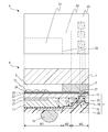
- Fig. 6 illustrates a modification of the image pickup device according to the first embodiment.
- Part A and part B of Fig. 6 are a partial plan view and a partial sectional view similar to part A and part B of Fig. 3.
- the same components as those in Fig. 3 are referred to as the same reference numerals and signs and the explanations of those same components will be omitted.
- An image pickup device is characterized in that the thickness T1 of the semiconductor substrate 11 in the first area A1, the thickness T2 of the semiconductor substrate 11 in the second area A2, and the thickness T3 of the semiconductor substrate 11 in the third area A3 have the relationship T1 > T2 > T3. That is, the thickness T3 of the semiconductor substrate 11 in the third area A3 in which the penetrating electrode 16 is formed is smaller than the thickness T1 of the semiconductor substrate 11 in the first area A1, which is a capturing area, and the thickness T2 of the semiconductor substrate 11 in the second area A2, which is between the first area A1 and the third area A3, corresponds to the thickness between the thickness T1 and the thickness T3. Namely, the semiconductor substrate 11 has a configuration including three thicknesses.
- a point in that the boundary across which the thickness of the semiconductor substrate 11 changes is arranged within the fixing area in which the fixing member 3 is arranged when the image pickup device is viewed from the light incident side is the same as in the image pickup device according to the first embodiment. That is, the boundary 20 with the second area A2 in which the thickness of the semiconductor substrate is smaller than the thickness of the semiconductor substrate in the first area A1 is arranged within the fixing area.
- the thickness T2 and the width W2 of the semiconductor substrate 11 in the second area A2 and the thickness T3 of the semiconductor substrate 11 in the third area A3 satisfy the relationships described in the first embodiment, the possibility of deformation and cracking of the semiconductor substrate 11 can further be reduced, thus achieving an image pickup device exhibiting a high reliability. It is desirable that the boundary at which the greatest thickness T1 of the semiconductor substrate 11 starts to decrease be arranged within the fixing area.
- Fig. 7 illustrates a modification of the image pickup device according to the first embodiment.
- Part A and part B of Fig. 7 are a partial plan view and a partial sectional view similar to part A and part B of Fig. 3.
- the same components as those in Fig. 3 are referred to as the same reference numerals and signs and the explanations of those same components will be omitted.
- An image pickup device is characterized in that a cross section of the semiconductor substrate 11 in the second area A2 has a tapered shape. That is, the image pickup device according to this embodiment has a configuration in which the thickness T3 of the semiconductor substrate 11 in the third area A3 where the penetrating electrode 16 is formed is smaller than the thickness T1 of the semiconductor substrate 11 in the first area, which is a capturing area, and in which the thickness T2 of the semiconductor substrate 11 in the second area A2, which is between the first area A1 and the third area A3, is changed so as to have a tapered shape.
- a point in that the boundary 20 across which the thickness of the semiconductor substrate 11 changes is arranged within the fixing area in which the fixing member 3 is arranged when the image pickup device is viewed from the light incident side is the same as in the first and second embodiments. That is, the boundary 20 with the second area A2 in which the thickness of the semiconductor substrate is smaller than the thickness of the semiconductor substrate in the first area A1 is arranged within the fixing area.
- the thickness T2 and the width W2 of the semiconductor substrate 11 in the second area A2 and the thickness T3 of the semiconductor substrate 11 in the third area A3 satisfy the relationships described in the first embodiment, the possibility of deformation and cracking of the semiconductor substrate 11 can further be reduced, thus achieving an image pickup device exhibiting a high reliability.
- Fig. 8 illustrates an example of a case where the image pickup device according to the first, second, or third embodiment of the present invention is applied to an image pickup module to be used in a camera.
- An image pickup device 800 is installed on a circuit board 807 made of ceramics, silicon, or the like, and the image pickup device 800 is sealed within a cover member 804.
- the circuit board 807 is electrically connected to the image pickup device 800.
- An optical portion 805 that captures light and an optical low-pass filter 806 are arranged above the image pickup device 800.
- the cover member 804 is covered with an image pickup lens 802 and a lens-barrel member 801 fixing the image pickup lens 802, and the cover member 804 is well sealed with the lens-barrel member 801, the image pickup lens 802, and the circuit board 807.
- the image pickup device not only the image pickup device according to an embodiment of the present invention but also an image pickup signal processing circuit, an analog-to-digital (A/D) converter, and a module controller may be installed on the circuit board 807. These units may be formed on the same semiconductor substrate as that of the image pickup device in the same processing step as that in the image pickup device.
- the optical low-pass filter may be included in the image pickup device and arranged between the transparent member and the image pickup element chip.
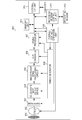
- Fig. 9 is a block diagram illustrating a case where the image pickup device according to the first, second, or third embodiment of the present invention is applied to a digital camera, which is an example of an image pickup system.
- a configuration for causing a solid-state image pickup element 904, which is an image pickup device, to capture light includes a shutter 901, an image pickup lens 902, and a diaphragm 903.
- the shutter 901 controls exposure to the solid-state image pickup element 904.
- Incident light passes through the image pickup lens 902 and an image is formed on the solid-state image pickup element 904. At this time, the amount of light is controlled by the diaphragm 903.
- a signal output from the solid-state image pickup element 904 in accordance with the captured light is processed in an image pickup signal processing circuit 905, and an A/D converter 906 converts an analog signal into a digital signal.
- the output digital signal is subjected to arithmetic processing in a signal processor 907, and captured image data is generated.
- the captured image data can be stored in a memory unit 910 arranged in the digital camera and can be transmitted to an external device, such as a computer or a printer, via an external I/F unit 913, in accordance with an operation mode set by a user.
- the captured image data can be recorded via a recording medium control I/F unit 911 on a recording medium 912 that can be removable from the digital camera.
- the solid-state image pickup element 904, the image pickup signal processing circuit 905, the A/D converter 906, and the signal processor 907 are controller by a timing generator 908.
- the overall system is controlled by an overall control/operation unit 909. Such a system may be formed on the same semiconductor substrate as that of the solid-state image pickup element 904 in the same processing step as that in the solid-state image pickup element 904.
- the possibility of deformation and cracking of a semiconductor substrate can be reduced, and an image pickup device and an image pickup system exhibiting a high reliability can be provided.
Landscapes
- Engineering & Computer Science (AREA)
- Physics & Mathematics (AREA)
- Power Engineering (AREA)
- Electromagnetism (AREA)
- Condensed Matter Physics & Semiconductors (AREA)
- General Physics & Mathematics (AREA)
- Computer Hardware Design (AREA)
- Microelectronics & Electronic Packaging (AREA)
- Multimedia (AREA)
- Signal Processing (AREA)
- Solid State Image Pick-Up Elements (AREA)
- Transforming Light Signals Into Electric Signals (AREA)
Abstract
Priority Applications (2)
| Application Number | Priority Date | Filing Date | Title |
|---|---|---|---|
| CN201180040856.6A CN103081105B (zh) | 2010-08-23 | 2011-08-05 | 图像拾取装置、图像拾取模块和照相机 |
| US13/817,755 US9111826B2 (en) | 2010-08-23 | 2011-08-05 | Image pickup device, image pickup module, and camera |
Applications Claiming Priority (2)
| Application Number | Priority Date | Filing Date | Title |
|---|---|---|---|
| JP2010186070A JP2012044091A (ja) | 2010-08-23 | 2010-08-23 | 撮像装置、撮像モジュール及びカメラ |
| JP2010-186070 | 2010-08-23 |
Publications (1)
| Publication Number | Publication Date |
|---|---|
| WO2012026074A1 true WO2012026074A1 (fr) | 2012-03-01 |
Family
ID=45723098
Family Applications (1)
| Application Number | Title | Priority Date | Filing Date |
|---|---|---|---|
| PCT/JP2011/004452 WO2012026074A1 (fr) | 2010-08-23 | 2011-08-05 | Dispositif et module de capture d'image et appareil photographique |
Country Status (4)
| Country | Link |
|---|---|
| US (1) | US9111826B2 (fr) |
| JP (1) | JP2012044091A (fr) |
| CN (1) | CN103081105B (fr) |
| WO (1) | WO2012026074A1 (fr) |
Cited By (1)
| Publication number | Priority date | Publication date | Assignee | Title |
|---|---|---|---|---|
| US20130277788A1 (en) * | 2012-04-24 | 2013-10-24 | Sony Corporation | Imaging unit and imaging device |
Families Citing this family (4)
| Publication number | Priority date | Publication date | Assignee | Title |
|---|---|---|---|---|
| JP2014216476A (ja) * | 2013-04-25 | 2014-11-17 | 凸版印刷株式会社 | 固体撮像装置及びその製造方法 |
| US20140326856A1 (en) * | 2013-05-06 | 2014-11-06 | Omnivision Technologies, Inc. | Integrated circuit stack with low profile contacts |
| EP3207566A4 (fr) * | 2014-10-13 | 2018-08-29 | Bio-rad Laboratories, Inc. | Fenêtre de capteur d'image chauffée |
| CN105467638A (zh) * | 2016-01-08 | 2016-04-06 | 豪威半导体(上海)有限责任公司 | 一种lcos结构及制造方法 |
Citations (3)
| Publication number | Priority date | Publication date | Assignee | Title |
|---|---|---|---|---|
| JP2001351997A (ja) * | 2000-06-09 | 2001-12-21 | Canon Inc | 受光センサーの実装構造体およびその使用方法 |
| JP2007305804A (ja) * | 2006-05-11 | 2007-11-22 | Olympus Corp | 半導体装置、該半導体装置の製造方法 |
| JP2010067872A (ja) * | 2008-09-12 | 2010-03-25 | Nikon Corp | パッケージ及びそれを用いた光電変換装置 |
Family Cites Families (14)
| Publication number | Priority date | Publication date | Assignee | Title |
|---|---|---|---|---|
| US6943423B2 (en) * | 2003-10-01 | 2005-09-13 | Optopac, Inc. | Electronic package of photo-image sensors in cellular phone camera modules, and the fabrication and assembly thereof |
| JP4198072B2 (ja) * | 2004-01-23 | 2008-12-17 | シャープ株式会社 | 半導体装置、光学装置用モジュール及び半導体装置の製造方法 |
| JP4344759B2 (ja) | 2007-06-15 | 2009-10-14 | シャープ株式会社 | 固体撮像素子およびその製造方法、固体撮像装置、電子情報機器 |
| JP2009099591A (ja) * | 2007-10-12 | 2009-05-07 | Toshiba Corp | 固体撮像素子及びその製造方法 |
| JP4799542B2 (ja) * | 2007-12-27 | 2011-10-26 | 株式会社東芝 | 半導体パッケージ |
| JP4799543B2 (ja) * | 2007-12-27 | 2011-10-26 | 株式会社東芝 | 半導体パッケージ及びカメラモジュール |
| JP5690466B2 (ja) * | 2008-01-31 | 2015-03-25 | インヴェンサス・コーポレイション | 半導体チップパッケージの製造方法 |
| JP5009209B2 (ja) * | 2008-03-21 | 2012-08-22 | シャープ株式会社 | ウエハ状光学装置およびその製造方法、電子素子ウエハモジュール、センサウエハモジュール、電子素子モジュール、センサモジュール、電子情報機器 |
| JP5198150B2 (ja) * | 2008-05-29 | 2013-05-15 | 株式会社東芝 | 固体撮像装置 |
| JP5392458B2 (ja) | 2008-08-21 | 2014-01-22 | 株式会社ザイキューブ | 半導体イメージセンサ |
| JP5178569B2 (ja) * | 2009-02-13 | 2013-04-10 | 株式会社東芝 | 固体撮像装置 |
| US8355628B2 (en) * | 2009-03-06 | 2013-01-15 | Visera Technologies Company Limited | Compact camera module |
| KR20100130423A (ko) * | 2009-06-03 | 2010-12-13 | 삼성전자주식회사 | 웨이퍼-레벨 렌즈 모듈 및 이를 구비하는 촬상 모듈 |
| JP5709435B2 (ja) * | 2010-08-23 | 2015-04-30 | キヤノン株式会社 | 撮像モジュール及びカメラ |
-
2010
- 2010-08-23 JP JP2010186070A patent/JP2012044091A/ja active Pending
-
2011
- 2011-08-05 WO PCT/JP2011/004452 patent/WO2012026074A1/fr active Application Filing
- 2011-08-05 CN CN201180040856.6A patent/CN103081105B/zh active Active
- 2011-08-05 US US13/817,755 patent/US9111826B2/en active Active
Patent Citations (3)
| Publication number | Priority date | Publication date | Assignee | Title |
|---|---|---|---|---|
| JP2001351997A (ja) * | 2000-06-09 | 2001-12-21 | Canon Inc | 受光センサーの実装構造体およびその使用方法 |
| JP2007305804A (ja) * | 2006-05-11 | 2007-11-22 | Olympus Corp | 半導体装置、該半導体装置の製造方法 |
| JP2010067872A (ja) * | 2008-09-12 | 2010-03-25 | Nikon Corp | パッケージ及びそれを用いた光電変換装置 |
Cited By (1)
| Publication number | Priority date | Publication date | Assignee | Title |
|---|---|---|---|---|
| US20130277788A1 (en) * | 2012-04-24 | 2013-10-24 | Sony Corporation | Imaging unit and imaging device |
Also Published As
| Publication number | Publication date |
|---|---|
| JP2012044091A (ja) | 2012-03-01 |
| CN103081105B (zh) | 2016-02-10 |
| US20130141626A1 (en) | 2013-06-06 |
| CN103081105A (zh) | 2013-05-01 |
| US9111826B2 (en) | 2015-08-18 |
Similar Documents
| Publication | Publication Date | Title |
|---|---|---|
| US8351219B2 (en) | Electronic assembly for an image sensing device | |
| EP1942661A2 (fr) | Ensemble électronique pour dispositif détecteur d'images et son procédé de fabrication | |
| WO2017135062A1 (fr) | Dispositif à semi-conducteurs et procédé de fabrication, et équipement électronique | |
| JP2007116560A (ja) | 撮像装置及びその製造方法 | |
| US9111826B2 (en) | Image pickup device, image pickup module, and camera | |
| US20090147115A1 (en) | Solid-state image pick-up device, method for producing the same, and electronics device with the same | |
| EP3177003B1 (fr) | Module de caméra | |
| JP2011187482A (ja) | 固体撮像装置、光学装置用モジュール、及び固体撮像装置の製造方法 | |
| JP2009070912A (ja) | 固体撮像素子及び撮像装置 | |
| US10972642B2 (en) | Imager and imaging device | |
| US11019292B2 (en) | Imager and imaging device | |
| JP5479972B2 (ja) | 撮像装置 | |
| JP2009003058A (ja) | カメラモジュール、台座マウント及び撮像装置 | |
| JP7214870B2 (ja) | 撮像素子ユニット及び撮像装置 | |
| JP5514685B2 (ja) | 撮像モジュールおよび電子情報機器 | |
| JP6757862B2 (ja) | 撮像ユニット及び撮像装置 | |
| JP7427410B2 (ja) | 撮像装置及びカメラ | |
| JP6990317B2 (ja) | 撮像ユニット及び撮像装置 | |
| JP2009111130A (ja) | 撮像装置及びその製造方法 | |
| JP2013005116A (ja) | カメラモジュールおよびそれを備えた電子機器 | |
| JP2009070913A (ja) | 固体撮像素子及び撮像装置 | |
| JP2008311493A (ja) | 固体撮像素子およびその製造方法、固体撮像装置、電子情報機器 | |
| JP2007336368A (ja) | 撮像素子、表示素子 | |
| KR101026829B1 (ko) | 카메라 모듈 및 그 제조 방법 | |
| JP2011077554A (ja) | 半導体イメージセンサ・モジュールおよび半導体イメージセンサ・モジュールの製造方法 |
Legal Events
| Date | Code | Title | Description |
|---|---|---|---|
| WWE | Wipo information: entry into national phase |
Ref document number: 201180040856.6 Country of ref document: CN |
|
| 121 | Ep: the epo has been informed by wipo that ep was designated in this application |
Ref document number: 11819551 Country of ref document: EP Kind code of ref document: A1 |
|
| WWE | Wipo information: entry into national phase |
Ref document number: 13817755 Country of ref document: US |
|
| NENP | Non-entry into the national phase |
Ref country code: DE |
|
| 122 | Ep: pct application non-entry in european phase |
Ref document number: 11819551 Country of ref document: EP Kind code of ref document: A1 |