WO2012017868A1 - 金属錯体色素、光電変換素子及び光電気化学電池 - Google Patents
金属錯体色素、光電変換素子及び光電気化学電池 Download PDFInfo
- Publication number
- WO2012017868A1 WO2012017868A1 PCT/JP2011/067005 JP2011067005W WO2012017868A1 WO 2012017868 A1 WO2012017868 A1 WO 2012017868A1 JP 2011067005 W JP2011067005 W JP 2011067005W WO 2012017868 A1 WO2012017868 A1 WO 2012017868A1
- Authority
- WO
- WIPO (PCT)
- Prior art keywords
- group
- ring
- general formula
- dye
- metal complex
- Prior art date
- Legal status (The legal status is an assumption and is not a legal conclusion. Google has not performed a legal analysis and makes no representation as to the accuracy of the status listed.)
- Ceased
Links
- 0 CCC(N)=C*C(*C)=CC(*=I)=CC Chemical compound CCC(N)=C*C(*C)=CC(*=I)=CC 0.000 description 6
Images
Classifications
-
- C—CHEMISTRY; METALLURGY
- C09—DYES; PAINTS; POLISHES; NATURAL RESINS; ADHESIVES; COMPOSITIONS NOT OTHERWISE PROVIDED FOR; APPLICATIONS OF MATERIALS NOT OTHERWISE PROVIDED FOR
- C09B—ORGANIC DYES OR CLOSELY-RELATED COMPOUNDS FOR PRODUCING DYES, e.g. PIGMENTS; MORDANTS; LAKES
- C09B47/00—Porphines; Azaporphines
- C09B47/04—Phthalocyanines abbreviation: Pc
- C09B47/045—Special non-pigmentary uses, e.g. catalyst, photosensitisers of phthalocyanine dyes or pigments
-
- C—CHEMISTRY; METALLURGY
- C09—DYES; PAINTS; POLISHES; NATURAL RESINS; ADHESIVES; COMPOSITIONS NOT OTHERWISE PROVIDED FOR; APPLICATIONS OF MATERIALS NOT OTHERWISE PROVIDED FOR
- C09B—ORGANIC DYES OR CLOSELY-RELATED COMPOUNDS FOR PRODUCING DYES, e.g. PIGMENTS; MORDANTS; LAKES
- C09B47/00—Porphines; Azaporphines
- C09B47/04—Phthalocyanines abbreviation: Pc
- C09B47/06—Preparation from carboxylic acids or derivatives thereof, e.g. anhydrides, amides, mononitriles, phthalimide, o-cyanobenzamide
- C09B47/067—Preparation from carboxylic acids or derivatives thereof, e.g. anhydrides, amides, mononitriles, phthalimide, o-cyanobenzamide from phthalodinitriles naphthalenedinitriles, aromatic dinitriles prepared in situ, hydrogenated phthalodinitrile
- C09B47/0673—Preparation from carboxylic acids or derivatives thereof, e.g. anhydrides, amides, mononitriles, phthalimide, o-cyanobenzamide from phthalodinitriles naphthalenedinitriles, aromatic dinitriles prepared in situ, hydrogenated phthalodinitrile having alkyl radicals linked directly to the Pc skeleton; having carbocyclic groups linked directly to the skeleton
-
- C—CHEMISTRY; METALLURGY
- C09—DYES; PAINTS; POLISHES; NATURAL RESINS; ADHESIVES; COMPOSITIONS NOT OTHERWISE PROVIDED FOR; APPLICATIONS OF MATERIALS NOT OTHERWISE PROVIDED FOR
- C09B—ORGANIC DYES OR CLOSELY-RELATED COMPOUNDS FOR PRODUCING DYES, e.g. PIGMENTS; MORDANTS; LAKES
- C09B47/00—Porphines; Azaporphines
- C09B47/04—Phthalocyanines abbreviation: Pc
- C09B47/06—Preparation from carboxylic acids or derivatives thereof, e.g. anhydrides, amides, mononitriles, phthalimide, o-cyanobenzamide
- C09B47/067—Preparation from carboxylic acids or derivatives thereof, e.g. anhydrides, amides, mononitriles, phthalimide, o-cyanobenzamide from phthalodinitriles naphthalenedinitriles, aromatic dinitriles prepared in situ, hydrogenated phthalodinitrile
- C09B47/0675—Preparation from carboxylic acids or derivatives thereof, e.g. anhydrides, amides, mononitriles, phthalimide, o-cyanobenzamide from phthalodinitriles naphthalenedinitriles, aromatic dinitriles prepared in situ, hydrogenated phthalodinitrile having oxygen or sulfur linked directly to the skeleton
-
- C—CHEMISTRY; METALLURGY
- C09—DYES; PAINTS; POLISHES; NATURAL RESINS; ADHESIVES; COMPOSITIONS NOT OTHERWISE PROVIDED FOR; APPLICATIONS OF MATERIALS NOT OTHERWISE PROVIDED FOR
- C09B—ORGANIC DYES OR CLOSELY-RELATED COMPOUNDS FOR PRODUCING DYES, e.g. PIGMENTS; MORDANTS; LAKES
- C09B47/00—Porphines; Azaporphines
- C09B47/04—Phthalocyanines abbreviation: Pc
- C09B47/06—Preparation from carboxylic acids or derivatives thereof, e.g. anhydrides, amides, mononitriles, phthalimide, o-cyanobenzamide
- C09B47/067—Preparation from carboxylic acids or derivatives thereof, e.g. anhydrides, amides, mononitriles, phthalimide, o-cyanobenzamide from phthalodinitriles naphthalenedinitriles, aromatic dinitriles prepared in situ, hydrogenated phthalodinitrile
- C09B47/0676—Preparation from carboxylic acids or derivatives thereof, e.g. anhydrides, amides, mononitriles, phthalimide, o-cyanobenzamide from phthalodinitriles naphthalenedinitriles, aromatic dinitriles prepared in situ, hydrogenated phthalodinitrile having nitrogen atom(s) linked directly to the skeleton
-
- C—CHEMISTRY; METALLURGY
- C09—DYES; PAINTS; POLISHES; NATURAL RESINS; ADHESIVES; COMPOSITIONS NOT OTHERWISE PROVIDED FOR; APPLICATIONS OF MATERIALS NOT OTHERWISE PROVIDED FOR
- C09B—ORGANIC DYES OR CLOSELY-RELATED COMPOUNDS FOR PRODUCING DYES, e.g. PIGMENTS; MORDANTS; LAKES
- C09B47/00—Porphines; Azaporphines
- C09B47/04—Phthalocyanines abbreviation: Pc
- C09B47/06—Preparation from carboxylic acids or derivatives thereof, e.g. anhydrides, amides, mononitriles, phthalimide, o-cyanobenzamide
- C09B47/067—Preparation from carboxylic acids or derivatives thereof, e.g. anhydrides, amides, mononitriles, phthalimide, o-cyanobenzamide from phthalodinitriles naphthalenedinitriles, aromatic dinitriles prepared in situ, hydrogenated phthalodinitrile
- C09B47/0678—Preparation from carboxylic acids or derivatives thereof, e.g. anhydrides, amides, mononitriles, phthalimide, o-cyanobenzamide from phthalodinitriles naphthalenedinitriles, aromatic dinitriles prepared in situ, hydrogenated phthalodinitrile having-COOH or -SO3H radicals or derivatives thereof directly linked to the skeleton
-
- H—ELECTRICITY
- H01—ELECTRIC ELEMENTS
- H01G—CAPACITORS; CAPACITORS, RECTIFIERS, DETECTORS, SWITCHING DEVICES, LIGHT-SENSITIVE OR TEMPERATURE-SENSITIVE DEVICES OF THE ELECTROLYTIC TYPE
- H01G9/00—Electrolytic capacitors, rectifiers, detectors, switching devices, light-sensitive or temperature-sensitive devices; Processes of their manufacture
- H01G9/20—Light-sensitive devices
- H01G9/2059—Light-sensitive devices comprising an organic dye as the active light absorbing material, e.g. adsorbed on an electrode or dissolved in solution
-
- H—ELECTRICITY
- H10—SEMICONDUCTOR DEVICES; ELECTRIC SOLID-STATE DEVICES NOT OTHERWISE PROVIDED FOR
- H10K—ORGANIC ELECTRIC SOLID-STATE DEVICES
- H10K85/00—Organic materials used in the body or electrodes of devices covered by this subclass
- H10K85/30—Coordination compounds
- H10K85/311—Phthalocyanine
-
- H—ELECTRICITY
- H01—ELECTRIC ELEMENTS
- H01G—CAPACITORS; CAPACITORS, RECTIFIERS, DETECTORS, SWITCHING DEVICES, LIGHT-SENSITIVE OR TEMPERATURE-SENSITIVE DEVICES OF THE ELECTROLYTIC TYPE
- H01G9/00—Electrolytic capacitors, rectifiers, detectors, switching devices, light-sensitive or temperature-sensitive devices; Processes of their manufacture
- H01G9/20—Light-sensitive devices
- H01G9/2027—Light-sensitive devices comprising an oxide semiconductor electrode
- H01G9/2031—Light-sensitive devices comprising an oxide semiconductor electrode comprising titanium oxide, e.g. TiO2
-
- H—ELECTRICITY
- H10—SEMICONDUCTOR DEVICES; ELECTRIC SOLID-STATE DEVICES NOT OTHERWISE PROVIDED FOR
- H10K—ORGANIC ELECTRIC SOLID-STATE DEVICES
- H10K85/00—Organic materials used in the body or electrodes of devices covered by this subclass
- H10K85/30—Coordination compounds
- H10K85/381—Metal complexes comprising a group IIB metal element, e.g. comprising cadmium, mercury or zinc
-
- Y—GENERAL TAGGING OF NEW TECHNOLOGICAL DEVELOPMENTS; GENERAL TAGGING OF CROSS-SECTIONAL TECHNOLOGIES SPANNING OVER SEVERAL SECTIONS OF THE IPC; TECHNICAL SUBJECTS COVERED BY FORMER USPC CROSS-REFERENCE ART COLLECTIONS [XRACs] AND DIGESTS
- Y02—TECHNOLOGIES OR APPLICATIONS FOR MITIGATION OR ADAPTATION AGAINST CLIMATE CHANGE
- Y02E—REDUCTION OF GREENHOUSE GAS [GHG] EMISSIONS, RELATED TO ENERGY GENERATION, TRANSMISSION OR DISTRIBUTION
- Y02E10/00—Energy generation through renewable energy sources
- Y02E10/50—Photovoltaic [PV] energy
- Y02E10/542—Dye sensitized solar cells
Definitions
- the present invention relates to a metal complex dye, a photoelectric conversion element and a photoelectrochemical cell, which have high conversion efficiency and excellent durability.
- Photoelectric conversion elements are used in various optical sensors, copiers, solar cells and the like.
- Various systems such as those using metals, those using semiconductors, those using organic pigments and dyes, or combinations thereof are put into practical use for this photoelectric conversion element.
- a solar cell using non-depleting solar energy does not require fuel, and its full-scale practical use is expected greatly as it uses inexhaustible clean energy.
- silicon solar cells have been researched and developed for a long time. It is spreading due to the policy considerations of each country. However, silicon is an inorganic material, and its throughput and molecular modification are naturally limited.
- Patent Document 1 describes a dye-sensitized photoelectric conversion element using semiconductor fine particles sensitized with a ruthenium complex dye by applying this technique.
- ruthenium complex dyes are extremely expensive to use alone as a sensitizer, and there is a problem that ruthenium has a concern for supply.
- Patent Document 2 describes a metal complex dye having a porphyrin or porphyrazine skeleton.
- difficult to obtain metals such as lanthanoids and yttrium are used for the metal complex dyes. In addition, these metals are uneasy about safety.
- Patent Document 3 describes a metal complex dye having a porphyrin skeleton in which an aromatic ring having a carboxyl group is a pyrazine ring or a quinoxaline ring.
- Soret band Soret band
- the photoelectric conversion element is required to have high initial conversion efficiency, low decrease in conversion efficiency in long-term use, and excellent durability.
- the photoelectric conversion elements described in Patent Document 2 and Patent Document 3 are not sufficient.
- An object of the present invention is to provide a metal complex that can be used as a photoelectric conversion element and a photoelectrochemical cell having a wide light absorption wavelength range and excellent conversion efficiency and durability when used in a photoelectric conversion element and a photoelectrochemical cell. It is to provide a pigment. Furthermore, another subject of this invention is providing the photoelectric conversion element and photoelectrochemical cell excellent in conversion efficiency and durability.
- the present inventors have conducted intensive studies in view of the above problems. As a result, it has been found that the metal complex dye having a phthalocyanine skeleton has at least one aromatic ring having an acidic group, so that the Soret band in the ultraviolet region becomes longer and the light absorption wavelength region capable of photoelectric conversion is expanded. It was. Furthermore, it has been found that the durability of the photoelectric conversion element and the photoelectrochemical cell using this metal complex dye is improved by the relatively bulky aromatic ring having an acidic group and the aromatic ring having no acidic group. . The present invention has been made based on these findings.
- the LUMO energy level is lowered by extending the conjugation of the aromatic ring part with LUMO or the electron withdrawing heterocycle, and the light absorption wavelength range. Is estimated to expand.
- a metal complex dye represented by the following general formula (1) is provided.
- R 11 to R 14 each represent a substituent, and at least one of them represents an acidic group.
- A11 to a14 each represents a positive integer of 1 or more.
- M represents a metal or metal oxide.
- a to D represents an aromatic ring, and among the aromatic rings of A to D, the aromatic ring having an acidic group is a diphenylbenzene ring, a naphthalene ring, a phenylnaphthalene ring, an anthracene ring, or a phenanthrene.
- the aromatic ring having an acidic group is a ⁇ -electron deficient heteroaromatic ring, or a benzene ring to which a ⁇ -electron deficient heteroaromatic ring is bonded, or
- the number of aromatic rings having an acidic group among the aromatic rings A to D is one or two, ⁇ 1> or ⁇ 2 >
- the aromatic rings having no acidic group among the aromatic rings A to D are each independently a benzene ring, naphthalene ring, anthracene ring, phenanthrene ring, thiophene ring, or benzo
- the substituents represented by R 11 to R 14 other than the acidic group are each independently an alkyl group, an aryl group, a heterocyclic group, an alkyloxy group, an alkylthio group, an alkyl group.
- the metal complex dye according to any one of ⁇ 1> to ⁇ 5> which is a silyl group, an aryloxy group, a heteroaryloxy group, an arylthio group, a heteroarylthio group, an arylsilyl group, or a heteroarylsilyl group.
- ⁇ 7> The metal complex dye according to any one of ⁇ 1> to ⁇ 6>, wherein in formula (1), a11 to a14 are each independently an integer of 1 to 4.
- ⁇ 8> In the general formula (1), ⁇ M> wherein M is copper, zinc, tin, nickel, iron, cobalt, silicon, palladium, chloro-aluminum, magnesium, gallium, titanyloxy, or vanadyloxy.
- metal complex dye according to any one of to ⁇ 7>. ⁇ 9> Any one of the above ⁇ 1> to ⁇ 8>, wherein the metal complex dye represented by the general formula (1) is a metal complex dye represented by the following general formula (8) or (9): Metal complex dyes.
- a to D each represent an aromatic ring.
- a 1 and A 2 each independently represent an acidic group.
- D 1 to D 3 each independently represent an alkyl group, aryl A group, a heterocyclic group, an alkyloxy group, an alkylthio group, an alkylsilyl group, an aryloxy group, a heteroaryloxy group, an arylthio group, a heteroarylthio group or an arylsilyl group, and a heteroarylsilyl group.
- D21 to d23 represent a positive integer of 1 or more
- M represents a metal, a metal oxide, or a metal chloride.
- a dye for a photoelectric conversion element comprising the metal complex dye according to any one of ⁇ 1> to ⁇ 9>.
- a photoelectric conversion device comprising a photoreceptor layer having the metal complex dye according to any one of ⁇ 1> to ⁇ 9> and semiconductor fine particles.
- Mz represents a metal atom
- LL 1 represents a bidentate or tridentate ligand represented by the following General Formula (3)
- LL 2 represents the following General Formula (4). Represents the represented bidentate or tridentate ligand.
- X is an acyloxy group, an acylthio group, a thioacyloxy group, a thioacylthio group, an acylaminooxy group, a thiocarbamate group, a dithiocarbamate group, a thiocarbonate group, a dithiocarbonate group, a trithiocarbonate group, an acyl group, a thiocyanate group,
- a monodentate or bidentate ligand coordinated by a group selected from the group consisting of an isothiocyanate group, a cyanate group, an isocyanate group, a cyano group, an alkylthio group, an arylthio group, an alkoxy group and an aryloxy group, or a halogen atom Represents a monodentate or bidentate ligand selected from the group consisting of carbonyl, dialkyl ketone, 1,3-diketone, carbonamide, thiocarbonamide and thiour
- m1 represents an integer of 0 to 3, and when m1 is 2 or more, LL 1 may be the same or different.
- m2 represents an integer of 1 to 3, and when m2 is 2 or more, LL 2 may be the same or different.
- m3 represents an integer of 0 to 3, and when m3 is 2 or more, Xs may be the same or different, and Xs may be linked together.
- CI represents a counter ion in the general formula (2) when a counter ion is necessary to neutralize the charge.
- R 21 and R 22 each independently represent an acidic group.
- R 23 and R 24 each independently represent a substituent, and
- R 25 and R 26 each independently represent an alkyl group, an aryl group or a heterocyclic group.
- d1 and d2 each represents an integer of 0 to 5.
- L 1 and L 2 each independently represents a conjugated chain composed of at least one selected from the group consisting of an ethenylene group, an ethynylene group, and a divalent heterocyclic group.
- a1 and a2 each independently represent an integer of 0 to 3, and when a1 is 2 or more, R 21 may be the same or different, and when a2 is 2 or more, R 22 may be the same or different.
- b1 and b2 each independently represents an integer of 0 to 3.
- R 23 may be the same or different, and R 23 may be linked to each other to form a ring.
- R 24 may be the same or different, and R 24 may be linked to each other to form a ring.
- d3 represents 0 or 1.
- Za, Zb and Zc each independently represent a nonmetallic atom group capable of forming a 5- or 6-membered ring, and c represents 0 or 1. However, at least one of the rings formed by Za, Zb and Zc has an acidic group.
- ⁇ 13> The photoelectric conversion element according to ⁇ 11> or ⁇ 12>, which has a structure in which the photosensitive layer, the charge transfer body, and the counter electrode are stacked in this order on a conductive support.
- ⁇ 14> The photoelectric conversion element as described in any one of ⁇ 11> to ⁇ 13>, wherein the metal complex dye is adsorbed on the semiconductor fine particles.
- a photoelectrochemical cell comprising the photoelectric conversion element according to any one of ⁇ 11> to ⁇ 14>.
- the metal complex dye of the present invention By using the metal complex dye of the present invention, a photoelectric conversion element and a photoelectrochemical cell having high conversion efficiency and excellent durability can be provided.
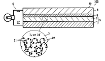
- the photoelectric conversion element 10 includes a conductive support 1, and a photosensitive layer 2, a charge transfer body layer 3, and a counter electrode 4 arranged in that order on the conductive support 1. .
- the conductive support 1 and the photoreceptor layer 2 constitute a light receiving electrode 5.
- the photoreceptor layer 2 has conductive fine particles 22 and a sensitizing dye 21, and the dye 21 is adsorbed on the conductive fine particles 22 at least partially (the dye is in an adsorption equilibrium state, Some may be present in the charge transfer layer).
- the conductive support 1 on which the photoreceptor layer 2 is formed functions as a working electrode in the photoelectric conversion element 10.
- the photoelectric conversion element 10 can be used as a battery for working in the external circuit 6 and can be operated as the photoelectrochemical battery 100.
- the light receiving electrode 5 is an electrode composed of the conductive support 1 and the photosensitive layer (semiconductor layer) 2 of the semiconductor fine particles 22 adsorbed by the dye 21 disposed on the conductive support 1.
- Light incident on the photoreceptor layer 2 excites the dye.
- the excited dye has high energy electrons. Therefore, the electrons are transferred from the dye 21 to the conduction band of the semiconductor fine particles 22 and further reach the conductive support 1 by diffusion.
- the molecule of the dye 21 is an oxidant.
- the electrons on the electrode return to the dye oxidant while working in the external circuit 6, thereby acting as a photoelectrochemical cell.
- the light receiving electrode 5 functions as a negative electrode of the battery.
- the upper and lower sides of the photoelectric conversion element do not need to be defined in particular, but in this specification, based on what is illustrated, the side of the counter electrode 4 serving as the light receiving side is the upper (top) direction, and the conductivity The side of the support 1 is the lower (bottom) direction.
- the photoelectric conversion element of the present invention has a photoreceptor layer having a porous semiconductor fine particle layer on which a dye described later is adsorbed on a conductive support.
- the photoreceptor layer is designed according to the purpose, and may be a single layer structure or a multilayer structure.
- the dye in the photoreceptor layer may be one kind or a mixture of many kinds of dyes, but at least one of them uses a metal complex dye described later.
- the photoconductor of the photoelectric conversion element of the present invention contains semiconductor fine particles adsorbed with the dye, has high sensitivity, and can be used as a photoelectrochemical cell, and high conversion efficiency can be obtained.
- R 11 to R 14 each represent a substituent, and at least one of them represents an acidic group.
- a11 to a14 each represents a positive integer of 1 or more.
- M represents a metal, a metal oxide, or a metal chloride.
- a to D represent an aromatic ring.
- M represents a metal chloride” means that a chloride ion is coordinated to the central metal.
- the acidic group itself such as a carboxy group, the acidic group may be substituted via a linking group within a range where a desired effect is exhibited, and this linking group is referred to as an acidic group.
- a to D represent aromatic rings.
- the aromatic ring may be an aromatic hydrocarbon ring or an aromatic heterocycle.
- the aromatic hydrocarbon ring of A, B, C and D in the general formula (1) is preferably a monocyclic or bicyclic aromatic hydrocarbon ring having 6 to 30 carbon atoms, and a monocyclic ring having 6 to 20 carbon atoms.
- a bicyclic aromatic hydrocarbon ring is more preferable, and a monocyclic or bicyclic aromatic hydrocarbon ring having 6 to 12 carbon atoms is more preferable.
- aromatic hydrocarbon ring examples include benzene ring, biphenyl ring, 1,3-diphenylbenzene ring, anthracene ring, naphthalene ring, 1-phenylnaphthalene ring, 2-phenylnaphthalene ring, anthracene ring, phenanthrene ring, naphthacene.
- aromatic hydrocarbon rings represented by A, B, C and D in the general formula (1) a benzene ring and a naphthalene ring are particularly preferable.
- the aromatic hydrocarbon ring may have a substituent, and examples of the substituent include the substituent T described later.
- an aromatic heterocyclic ring containing an oxygen atom, a nitrogen atom, a sulfur atom and / or a selenium atom as a hetero atom is preferable.
- the aromatic heterocycle include furan ring, pyrrole ring, thiophene ring, imidazole ring, pyrazole ring, triazole ring, triazine ring, indole ring, indazole ring, purine ring, thiazoline ring, thiazole ring, thiadiazole ring, benzo Thiophene ring, thienothiophene ring, bithiophene ring, oxazoline ring, oxazole ring, oxadiazole ring, phthalazine ring, naphthyridine ring, cinnoline ring, pteridine ring, phenanthroline ring, tetrazole ring, benzimi
- a ⁇ -electron deficient aromatic heterocycle is a fully unsaturated heterocycle containing a heteroatom and having a deficient ⁇ -electron, and the heteroatom is preferably a nitrogen atom.
- the mother nucleus structure includes pyridine, quinoline, isoquinoline, acridine, indolizine, phenanthridine, pyridazine containing two nitrogen atoms, pyrimidine, pyrazine, quinazoline, quinoxaline, 1, Examples include 5-naphthyridine, phenazine, sym-triazine containing 3 nitrogen atoms, asym-triazine, pterin containing 4 nitrogen atoms, and the like.
- a 5- or 6-membered aromatic heterocycle is preferable, and it may be condensed with another ring.
- aromatic heterocycle a quinoxaline ring, a thiophene ring, a pyridine ring, a pyrazine ring, a thiazole ring, a thienothiophene ring, and a benzthiazole ring are more preferable.
- the substituent T is, for example, an alkyl group (preferably having 1 to 20 carbon atoms, more preferably 1 to 12, particularly preferably 1 to 8, such as a methyl group, an ethyl group, an isopropyl group, or tert-butyl.
- an alkyl group preferably having 1 to 20 carbon atoms, more preferably 1 to 12, particularly preferably 1 to 8, such as a methyl group, an ethyl group, an isopropyl group, or tert-butyl.
- alkenyl group preferably 2-20 carbon atoms, more preferably 2-20 carbon atoms.
- alkynyl group preferably 2 to 20 carbon atoms, more preferably 2 To 12, particularly preferably 2 to 8, and examples thereof include a propargyl group and a 3-pentynyl group
- an aryl group preferably 6 to 30, more preferably 6 to 20, particularly preferably 6 to 12, and examples thereof include a phenyl group, a biphenyl group, and a naphthyl group.
- a substituted or unsubstituted amino group (preferably carbon The number of atoms is 0 to 20, more preferably 0 to 10, particularly preferably 0 to 6, and examples thereof include an amino group, a methylamino group, a dimethylamino group, a diethylamino group, and a dibenzylamino group.
- An alkoxy group (preferably having 1 to 20 carbon atoms, more preferably 1 to 12 carbon atoms, particularly preferably 1 to 8 carbon atoms such as a methoxy group, an ethoxy group, and a butoxy group), an aryloxy group (preferably The number of carbon atoms is 6 to 20, more preferably 6 to 16, and particularly preferably 6 to 12, and examples thereof include phenyloxy group and 2-naphthyloxy group.)
- Acyl group (preferably having 1 to 1 carbon atom) 20, more preferably 1 to 16, particularly preferably 1 to 12, and examples thereof include an acetyl group, a benzoyl group, a formyl group, and a pivaloyl group), an alkoxycarbonyl group (preferably having 2 to 20 carbon atoms, More preferably, it is 2 to 16, particularly preferably 2 to 12, and examples thereof include a methoxycarbonyl group and an ethoxycarbonyl group.
- An aryloxycarbonyl group (preferably having 7 to 20 carbon atoms, more preferably 7 to 16 carbon atoms, particularly preferably 7 to 10 carbon atoms such as a phenyloxycarbonyl group), an acyloxy group (preferably ) Has 2 to 20 carbon atoms, more preferably 2 to 16 carbon atoms, particularly preferably 2 to 10 carbon atoms, and examples thereof include an acetoxy group and a benzoyloxy group.
- An acylamino group (preferably having 2 to 20 carbon atoms, more preferably 2 to 16 carbon atoms, particularly preferably 2 to 10 carbon atoms such as an acetylamino group and a benzoylamino group), an alkoxycarbonylamino group (preferably 2-20 carbon atoms, more preferably 2-16 carbon atoms, particularly preferably 2-12 carbon atoms, such as a methoxycarbonylamino group), an aryloxycarbonylamino group (preferably having 7-20 carbon atoms, More preferably, it is 7 to 16, particularly preferably 7 to 12, and examples thereof include a phenyloxycarbonylamino group, etc.), a sulfonylamino group (preferably having 1 to 20 carbon atoms, more preferably 1 to 16, especially Preferably, it is 1 to 12, for example, methanesulfonylamino group, benzenesulfonyla ), Sulfamoyl groups (preferably having 0 to 20, more
- a carbamoyl group (preferably having 1 to 20 carbon atoms, more preferably 1 to 16 carbon atoms, particularly preferably 1 to 12 carbon atoms such as a carbamoyl group and a methylcarbamoyl group). , Diethylcarbamoyl group, phenylcarbamoyl group, etc.),
- alkylthio group preferably having 1 to 20 carbon atoms, more preferably 1 to 16 carbon atoms, particularly preferably 1 to 12 carbon atoms such as a methylthio group and an ethylthio group
- arylthio group preferably having 6 carbon atoms
- a sulfonyl group (preferably having 1 to 20 carbon atoms, more preferably 1 to 16 carbon atoms, particularly preferably 1 to 12, for example, mesyl group, tosyl group, etc.), sulfinyl group (preferably 1 to 20, more preferably 1 to 16, particularly preferably 1 to 12, such as methane Sulfinyl group, benzenesulfinyl group, etc.), ureido group (preferably having 1 to 20 carbon atoms, more preferably 1 to 16, particularly preferably 1 to 12, for example, ureido group, methylureido group, phenylureido group, etc.), phosphoric acid amide group (preferably having 1 to 20 carbon atoms, more preferably 1 to 12 carbon atoms) 16, particularly preferably 1 to 12, such as diethyl phosphate amide, phenyl phosphate amide,
- those having a hydrogen atom may be substituted with the above groups after removing this.
- Such functional groups include an alkylcarbonylaminosulfonyl group, an arylcarbonylaminosulfonyl group, an alkylsulfonylaminocarbonyl group, and an arylsulfonylaminocarbonyl group.
- Examples thereof include a methylsulfonylaminocarbonyl group, a p-methylphenylsulfonylaminocarbonyl group, an acetylaminosulfonyl group, and a benzoylaminosulfonyl group.
- substituents when there are two or more substituents, they may be the same or different. If possible, they may be linked together to form a ring.
- the aromatic ring having an acidic group is a diphenylbenzene ring, naphthalene ring, phenylnaphthalene ring, anthracene ring, phenanthrene ring, naphthacene ring, pentacene ring, Thiazolylbenzene ring, imidazolylbenzene ring, 1,3,4-thiadiazolylbenzene ring, 3-thiazolylnaphthalene ring, benzothiazole ring, ⁇ -electron deficient heteroaromatic ring (preferably pyridine ring, pyrimidine ring , Pyridazine ring, pyrazine ring, triazine ring, pyrazole ring, imidazole ring), ⁇ electron deficient heteroaromatic ring (preferably pyridine ring, pyrimidine ring, pyridazine ring, pyra
- the number of aromatic rings having an acidic group is preferably 1 or 2.
- the aromatic rings having no acidic group are each independently a benzene ring, naphthalene ring, anthracene ring, phenanthrene ring, thiophene ring or benzothiophene ring. It is preferable that
- the acidic group (substituent having a dissociative proton) represented by R 11 to R 14 is not particularly limited, and is a carboxy group, phosphonic acid group, sulfo group, sulfonic acid group, hydroxyl group, hydroxamic acid group, phosphoryl group.
- limiting in particular as said salt Any of organic salt and inorganic salt may be sufficient.
- Typical examples include alkali metal ions (lithium, sodium, potassium, etc.), alkaline earth metal ions (magnesium, calcium, etc.), ammonium, alkylammonium (eg, diethylammonium, tetrabutylammonium, etc.), pyridinium, alkylpyridinium ( Examples thereof include salts of methylpyridinium), guanidinium, tetraalkylphosphonium and the like.
- the acidic group is preferably a carboxyl group, a sulfonic acid group, a phosphoryl group or a phosphonyl group, and more preferably a carboxyl group.
- the substituent represented by R 11 to R 14 other than the acidic group is preferably an alkyl group (preferably a linear, branched or cyclic substituted or unsubstituted group having 1 to 20 carbon atoms).
- the substituent is preferably an n-hexyl group, 2-ethyl-hexyl group, t-octyl group, nonyl group or the like), an aryl group (preferably a substituent having 6 to 20 carbon atoms). Or an unsubstituted aryl group.
- Preferred examples of the substituent include an alkyl group, an alkylamino group, an alkyloxy group, and an alkylthio group), a heterocyclic group (preferably a substituted or unsubstituted group having 3 to 20 carbon atoms).
- a substituted heterocyclic group, and preferred examples of the substituent include an alkyl group, an alkylamino group, an alkyloxy group, an alkylthio group, and the like.
- alkylthio group (preferably a linear, branched, or cyclic substituted or unsubstituted alkylthio group having 1 to 20 carbon atoms.
- the substituent is preferably an alkyl group, an alkylamino group, an alkyloxy group, or an alkylthio group.
- An alkylsilyl group (preferably a linear, branched, or cyclic substituted or unsubstituted alkylsilyl group having 1 to 20 carbon atoms.
- the substituent is preferably an alkyl group, an alkylamino group, an alkyl group.
- Preferred examples of the substituent include an alkyl group, an alkylamino group, an alkyloxy group, an alkylthio group, and the like, and a heteroaryloxy group (preferably having 3 to 20 carbon atoms).
- a substituted or unsubstituted heteroaryloxy group preferably an alkyl group, an alkylamino group, an alkyloxy group, an alkylthio group, etc.
- an arylthio group preferably a substituent having 6 to 20 carbon atoms
- an unsubstituted arylthio group and preferable examples of the substituent include an alkyl group, an alkylamino group, an alkyloxy group, and an alkylthio group
- a heteroarylthio group preferably a substituted or substituted group having 3 to 20 carbon atoms
- An unsubstituted heteroarylthio group preferably alkyl A group, an alkylamino group, an alkyloxy group, an alkylthio group, etc.
- an arylsilyl group preferably a substituted or unsubstituted arylsilyl group having 6 to 20 carbon atoms.
- alkylamino group alkyloxy group, alkylthio group, etc.
- heteroarylsilyl group preferably a substituted or unsubstituted heteroarylsilyl group having 3 to 20 carbon atoms, preferably as a substituent
- a11 to a14 represent an integer of 1 or more.
- a11 to a14 preferably represent an integer of 1 to 4, more preferably 1 or 2.
- M represents a metal, a metal oxide, or a metal chloride.
- metal chloride aluminum chloride (Al—Cl), stannic chloride (Sn—Cl 2 ), manganese chloride (Mn—Cl), titanium chloride (Ti—Cl 2 ), gallium chloride (Ga—). Cl), indium chloride (In—Cl), and the like.
- stannic chloride and aluminum chloride are preferred.
- the aromatic ring having an acidic group preferably has 1 to 4 acidic groups, and more preferably has 1 to 2 acidic groups.
- the metal complex dye represented by the general formula (1) is preferably a metal complex dye represented by the following general formula (8) or (9). Among these metal complex dyes, the metal complex dye represented by the general formula (8) is more preferable.
- A, B, C, D, and M are synonymous with those in the general formula (1), and preferred ranges are also the same.
- a 1 and A 2 each independently represent an acidic group, and may be the same or different. Specific examples of the acidic group include those exemplified as the acidic groups of R 11 to R 14 in the general formula (1), and the preferred ranges are also the same.
- D 1 to D 3 are each independently an alkyl group, aryl group, heterocyclic group, alkyloxy group, alkylthio group, alkylsilyl group, aryloxy group, heteroaryloxy group Represents an arylthio group, a heteroarylthio group, an arylsilyl group, or a heteroarylsilyl group.
- a21 to a22 represent an integer of 1 or more.
- a21 to a22 preferably represent an integer of 1 to 4, more preferably 1 or 2.
- d21 to d23 represent an integer of 1 or more.
- d21 to d23 are preferably an integer of 1 to 4, more preferably 1 to 3.
- the maximum absorption wavelength (Q band peak) in the solution is preferably in the range of 500 to 1500 nm, and more preferably in the range of 600 to 1200 nm. .
- the peak of the Soret band is preferably in the range of 200 to 600 nm, and more preferably in the range of 300 to 500 nm.
- the light absorption wavelength region of the dye represented by the general formula (1) at a wavelength of 400 nm or more is preferably in the range of 400 to 1500 nm, and more preferably in the range of 400 to 1200 nm.
- the wavelength difference between the peak in the Q band and the peak in the Soret band is preferably in the range of 100 to 400 nm, and more preferably in the range of 150 to 350 nm.
- the metal complex dye represented by the general formula (1) of the present invention includes two or more aromatic dinitrile compounds and / or diiminopyrrole compounds represented by the following general formula (5), for example, as shown in the following scheme (I). It can synthesize
- the general formula (5) after reacting two or more aromatic dinitrile compounds and / or diiminopyrrole derivatives with a metal derivative represented by the general formula (6), the general formula (5) It can synthesize
- the present invention is not limited to these.
- R A represents a substituent
- R B represents a ⁇ -electron deficient heteroaromatic ring with an acidic group in scheme (I)
- an acidic group in scheme (II) Alternatively, it represents a ⁇ -electron deficient heteroaromatic ring with an acidic group.
- N1 and N2 represent an integer of 1 or more.
- M is synonymous with that of the general formula (1).
- M has the same meaning as M in general formula (1).
- X ′ represents a monovalent or divalent ligand such as a halogen atom, acetate ion, acetylacetonate, or oxygen, and e represents an integer of 1 to 4.
- M ′-(Y) f M ′-(Y) f
- M ′ represents an alkali metal
- Y represents a monovalent or divalent ligand such as a halogen atom, acetate ion, acetylacetonate, alcoholate, oxygen
- f represents 1 to 4. Represents an integer.
- the mixing ratio is not particularly limited, but a molar ratio of 1: 4 to 4: 1 is preferable. .
- the amount of the metal derivative and aromatic dinitrile used is not particularly limited, but a molar ratio of 1: 3 to 1: 6 is preferable.
- the reactions shown in Schemes (I) and (II) are usually performed in the presence of a solvent.
- the solvent is not particularly limited, but an organic solvent having a boiling point of 80 ° C or higher, preferably 95 ° C or higher is preferably used.
- the amount of the solvent to be used is not particularly limited, but it is preferably 1 to 100 times
- a catalyst may be used.
- the catalyst is not particularly limited, and examples thereof include 1,8-diazabicyclo [5.4.0] -7-undecene (DBU) and ammonium molybdate.
- the amount of the catalyst added is not particularly limited, but is preferably 0.1 to 10 times mol, more preferably 0.5 to 2 times mol based on 1 mol of the aromatic dinitrile compound and / or diiminopyrrole compound. .
- the reaction temperature of the reactions shown in Schemes (I) and (II) is not particularly limited, but is preferably 80 to 300 ° C, more preferably 90 to 250 ° C, and particularly preferably 110 to 230 ° C. If the reaction temperature is too low, the reaction rate becomes extremely slow, and if it is too high, the aromatic dinitrile compound and / or the diiminopyrrole compound may be decomposed.
- the reaction time of the reactions shown in Schemes (I) and (II) is not particularly limited, but is preferably 2 to 20 hours, more preferably 5 to 15 hours, and particularly preferably 5 to 10 hours. If the reaction time is too short, the amount of unreacted raw materials increases. If the reaction time is too long, the aromatic dinitrile compound and / or the diiminopyrrole compound may be decomposed.
- the metal complex dye represented by the general formula (1) of the present invention can also be synthesized as shown in the following scheme (I ′) or (II ′). Specifically, two or more aromatic dinitrile compounds and / or diiminopyrrole compounds containing an aromatic dinitrile compound and / or diiminopyrrole compound having an acidic group (ester group) protected with a protecting group are described above. It can be synthesized by reacting with a metal derivative represented by the general formula (5) and hydrolyzing the resulting intermediate using an alkali metal hydroxide salt represented by the following general formula (7). it can.
- two or more aromatic dinitrile compounds and / or diiminopyrrole derivatives including an aromatic dinitrile compound and / or a diiminopyrrole compound having an acidic group (ester group) protected by a protecting group are represented by the above general formula ( After reacting with the metal derivative represented by 6), the product is reacted with the metal derivative represented by the general formula (5), and the resulting intermediate is hydroxylated with an alkali metal represented by the following general formula (7). It can be synthesized by hydrolysis using a physical salt.
- R A ′ represents an acidic group protected with a protecting group
- R A , R B , N1, N2 and M are the same as those in Schemes (I) and (II). It is synonymous.
- M ′ (OH) g M ′ (OH) g
- M ′ represents an alkali metal
- g represents an integer of 1 to 2.
- Two kinds of aromatic dinitrile compounds and / or diiminopyrrole compounds including an aromatic dinitrile compound and / or a diiminopyrrole compound having an acidic group (ester group) protected with a protecting group are reacted to form the metal of the present invention.
- the mixing ratio is not particularly limited, but a molar ratio of 1: 4 to 4: 1 is preferable.
- the amount of the metal derivative and the aromatic dinitrile compound and / or diiminopyrrole compound is not particularly limited, but is 1: 3 to 1: 6 in molar ratio. Is preferred.
- the amount of alkali metal hydroxide salt used is not particularly limited, but (t ⁇ N1) mol or more is used with respect to t mol of the intermediate. preferable.
- water or a mixed solvent of these solvents and a hydrocarbon solvent such as toluene, xylene, hexane, heptane, or the like can also be used.
- the amount of the solvent used is not particularly limited, but is preferably 1 to 100 times by mass of the aromatic dinitrile compound and / or diiminopyrrole compound, and more preferably 3 to 60 times by mass.
- reaction temperature of the reactions shown in Schemes (I ') and (II') there are no particular limitations on the reaction temperature of the reactions shown in Schemes (I ') and (II'), but 20 to 300 ° C is preferable, 40 to 200 ° C is more preferable, and 60 to 150 ° C is particularly preferable. If the reaction temperature is too low, the reaction rate becomes extremely slow, and if it is too high, decomposition may occur.
- reaction time of the reactions shown in Schemes (I ′) and (II ′) is not particularly limited, but is preferably 0.5 to 100 hours, more preferably 2 to 50 hours, and particularly preferably 5 to 40 hours. If the reaction time is too short, unreacted raw materials increase, and if it is too long, decomposition may occur.
- the product obtained by the reaction can be used as the metal complex dye of the present invention after being treated according to a post-treatment method of a normal organic synthesis reaction and then purified or not purified.
- the product liberated from the reaction system is not purified, or recrystallization, column chromatography (for example, gel permeation chromatography (SEPHADEXTMLH-20: manufactured by Pharmacia), HPLC, etc. is used alone or in combination.
- SEPHADEXTMLH-20 manufactured by Pharmacia
- HPLC etc.
- the reaction solvent is distilled off or not, poured into water or ice, neutralized or neutralized, and the liberated product is not purified or recrystallized, column
- the metal complex dye of the present invention can be provided after performing the operation of purification by chromatography, HPLC or the like alone or in combination.
- the reaction solvent is distilled off or not, and the product extracted with an organic solvent / water solution is neutralized with or without neutralization by opening in water or ice.
- the metal complex dye of the present invention can be provided without purification, or after performing purification by crystallization, column chromatography, or HPLC alone or in combination.
- a compound a complex and a pigment
- dye in addition to the said compound itself, the salt, complex (when it is other than a complex), and the meaning containing the ion are used. Moreover, it is the meaning including the compound modified with the predetermined form in the range with the desired effect.
- a substituent that does not specify substitution / non-substitution means that the group may have an arbitrary substituent. This is also synonymous for compounds that do not specify substitution / non-substitution.
- Preferred substituents include the above-described substituent T.
- the photoelectric conversion element of the present invention includes a photoreceptor layer having a metal complex dye and semiconductor fine particles.
- Mz represents a metal atom.
- Mz is preferably a metal capable of tetracoordinate or hexacoordinate, and more preferably Ru, Fe, Os, Cu, W, Cr, Mo, Ni, Pd, Pt, Co, Ir, Rh, Re, Mn Or Zn, particularly preferably Ru, Os, Zn or Cu, and most preferably Ru.
- X is an acyloxy group, an acylthio group, a thioacyloxy group, a thioacylthio group, an acylaminooxy group, a thiocarbamate group, a dithiocarbamate group, a thiocarbonate group, a dithiocarbonate group, a trithiocarbonate group, an acyl group, a thiocyanate group,
- a monodentate or bidentate ligand coordinated by a group selected from the group consisting of an isothiocyanate group, a cyanate group, an isocyanate group, a cyano group, an alkylthio group, an arylthio group, an alkoxy group and an aryloxy group, or a halogen atom Represents a monodentate or bidentate ligand selected from the group consisting of carbonyl, dialkyl ketone, 1,3-diketone, carbonamide, thiocarbonamide and thiour
- the ligand LL 1 represents a bidentate or tridentate ligand represented by the following general formula (3), and is preferably a bidentate ligand.
- M1 representing the number of the ligand LL 1 is an integer of 0 to 3, preferably 1 to 3, and more preferably 1.
- m1 is 2 or more, the plurality of LL 1 may be the same or different. Therefore, the ligand LL 1 and / or the ligand LL 2 are coordinated to the metal atom Mz.
- R 21 and R 22 each independently represent an acidic group such as a carboxyl group, a sulfonic acid group, a hydroxyl group, a hydroxamic acid group (preferably a hydroxamic acid group having 1 to 20 carbon atoms, For example, —CONHOH, —CONCH 3 OH, etc.), phosphoryl groups (eg, —OP (O) (OH) 2 etc.) and phosphonyl groups (eg, —P (O) (OH) 2 etc.), and salts thereof It is done.
- they are a carboxyl group and a phosphonyl group, More preferably, a carboxyl group and these salts are mentioned.
- the acidic group represented by R 21 and R 22 may be substituted with any carbon atom on the pyridine ring.
- R 23 and R 24 each independently represent a substituent.
- substituents include an alkyl group (preferably an alkyl group having 1 to 20 carbon atoms such as methyl, ethyl, isopropyl, t-butyl, pentyl, heptyl, 1-ethylpentyl, benzyl, 2-ethoxyethyl).
- alkenyl groups preferably alkenyl groups having 2 to 20 carbon atoms such as vinyl, allyl, oleyl etc.
- alkynyl groups preferably alkynyl groups having 2 to 20 carbon atoms such as Ethynyl, butadiynyl, phenylethynyl, etc.
- a cycloalkyl group preferably a cycloalkyl group having 3 to 20 carbon atoms, such as cyclopropyl, cyclopentyl, cyclohexyl, 4-methylcyclohexyl, etc.
- an aryl group preferably having a carbon atom number
- 6-26 aryl groups such as phenyl, 1-naphth , 4-methoxyphenyl, 2-chlorophenyl, 3-methylphenyl, etc.
- a heterocyclic group preferably a heterocyclic group having 2 to 20 carbon atoms, such as 2-pyridy
- amino group preferably an amino group having 0 to 20 carbon atoms such as amino, N, N-dimethylamino, N, N-diethylamino, N-ethylamino, anilino, etc.
- a sulfonamide group preferably a carbon atom
- a sulfonamido groups such as N, N-dimethylsulfonamido and N-phenylsulfonamido
- acyloxy groups preferably acyloxy groups having 1 to 20 carbon atoms such as acetyloxy, benzoyloxy and the like
- a carbamoyl group preferably a carbamoyl group having 1 to 20 carbon atoms, such as N, N-dimethylcarbamoyl, N-phenylcarbamoyl, etc.
- an acylamino group preferably an acylamino group having 1 to 20 carbon atoms, such as Acetylamino, benzoy
- an alkyl group, an alkenyl group, an aryl group, a heterocyclic group, an alkoxy group, an aryloxy group, an alkoxycarbonyl group, an amino group, an acylamino group, a cyano group, and a halogen atom are preferable, and an alkyl group, an alkenyl group, A heterocyclic group, an alkoxy group, an alkoxycarbonyl group, an amino group, an acylamino group, and a cyano group are more preferable.
- the ligand LL 1 contains an alkyl group, an alkenyl group or the like, these may be linear or branched, and may be substituted or unsubstituted. Further, when the ligand LL 1 contains an aryl group, a heterocyclic group or the like, they may be monocyclic or condensed and may be substituted or unsubstituted.
- R 25 and R 26 each independently represents an aryl group or a heterocyclic group.
- the aryl group is preferably an aryl group having 6 to 30 carbon atoms (preferably 6 to 24, more preferably 6 to 18), and examples thereof include phenyl, substituted phenyl, naphthyl, and substituted naphthyl.
- the heterocyclic group is preferably a heterocyclic group having 3 to 30 carbon atoms (preferably 3 to 24, more preferably 3 to 16), such as 2-thienyl, 2-pyrrolyl, 2-imidazolyl, 1 -Imidazolyl, 4-pyridyl, 3-indolyl).
- R 25 and R 26 are preferably a heterocyclic group having 1 to 3 electron donating groups, and more preferably thienyl.
- the electron donating group is preferably an alkyl group, an alkenyl group, an alkynyl group, a cycloalkyl group, an alkoxy group, an aryloxy group, an amino group, an acylamino group (preferred examples are the same as those for R 23 and R 24 ) or a hydroxyl group. More preferably an alkyl group, an alkoxy group, an amino group or a hydroxyl group, particularly preferably an alkyl group.
- R 25 and R 26 may be the same or different, but are preferably the same.
- R 25 and R 26 may be directly bonded to the pyridine ring.
- R 25 and R 26 may be bonded to the pyridine ring via L 1 and / or L 2 .
- L 1 and L 2 are each independently at least one selected from the group consisting of a substituted or unsubstituted ethenylene group, a substituted or unsubstituted ethynylene group, and a substituted or unsubstituted divalent heterocyclic group. Represents a conjugated chain.
- the substituent is preferably an alkyl group, and more preferably a methyl group.
- L 1 and L 2 are each independently preferably a conjugated chain having 2 to 6 carbon atoms, more preferably ethenylene, butadienylene, ethynylene, butadienylene, methylethenylene or dimethylethenylene, particularly ethenylene or butadienylene.
- ethenylene is most preferred.
- L 1 and L 2 may be the same or different, but are preferably the same.
- each double bond may be a trans isomer, a cis isomer, or a mixture thereof.
- d1 and d2 each represent an integer of 0 to 5, preferably an integer of 0 to 3, and more preferably an integer of 0 to 2.
- d3 represents 0 or 1, and is preferably 1.
- a1 and a2 each independently represents an integer of 0 to 3.
- a1 is may be the R 21 when two or more be the same or different, R 22 when a2 is 2 or more may be the same or different.
- a1 is preferably 0 or 1
- a2 is preferably an integer of 0-2.
- a2 is preferably 1 or 2
- d3 is 1, a2 is preferably 0 or 1.
- the sum of a1 and a2 is preferably an integer of 0-2.
- the ring to be formed include a benzene ring, a pyridine ring, a thiophene ring, a pyrrole ring, a cyclohexane ring, a cyclopentane ring and the like.
- m1 in the general formula (3) is preferably 2 or 3, and more preferably 2.
- LL 2 represents a bidentate or tridentate ligand represented by the following general formula (4).
- LL 2 is preferably a bidentate ligand.
- M2 representing the number of ligands LL 2 is an integer of 1 to 3, and preferably 1 or 2.
- m2 is LL 2 when two or more may be the same or different.
- Za, Zb and Zc each independently represent a nonmetallic atom group capable of forming a 5-membered ring or a 6-membered ring.
- the formed 5-membered or 6-membered ring may be substituted or unsubstituted, and may be monocyclic or condensed.
- Za, Zb and Zc are preferably composed of a carbon atom, a hydrogen atom, a nitrogen atom, an oxygen atom, a sulfur atom, a phosphorus atom and / or a halogen atom, and preferably form an aromatic ring.
- the 5-membered ring examples include an imidazole ring, an oxazole ring, a thiazole ring, and a triazole ring.
- the 6-membered ring it is preferable to form a pyridine ring, a pyrimidine ring, a pyridazine ring or a pyrazine ring. Of these, an imidazole ring or a pyridine ring is more preferable.
- At least one of the rings formed by Za, Zb and Zc has an acidic group.
- acidic groups include carboxyl groups, sulfonic acid groups, hydroxyl groups, hydroxamic acid groups, phosphoryl groups and phosphonyl groups, sulfino groups, sulfinyl groups, phosphinyl groups, phosphono groups, thiol groups, and sulfonyl groups, and salts thereof. Can be mentioned. Among these, a carboxyl group, a phosphoryl group, or a phosphonyl group is preferable, and a carboxyl group is more preferable.
- the acidic group may be directly bonded to the ring formed by Za, Zb or Zc, or may be bonded to the ring formed by Za, Zb or Zc through a linking group.
- the linking group is not particularly limited, and examples thereof include a methylene group, an ethenylene group, an ethynylene group, an arylene group, a heteroarylene group, or a linking group obtained by combining these linking groups.
- c represents 0 or 1. c is preferably 0.
- the ligand LL 2 represented by the general formula (4) include an alkyl group, an alkenyl group or the like, they may be linear or branched and may be unsubstituted substituted. Further, LL 2 is an aryl group, when containing heterocyclic group, they may be a condensed ring may be monocyclic or unsubstituted substituted.
- X represents a monodentate or bidentate ligand.
- M3 representing the number of ligands X represents an integer of 0 to 2, and m3 is preferably 1 or 2.
- M3 is preferably 2 when X is a monodentate ligand, and m3 is preferably 1 when X is a bidentate ligand.
- Xs may be the same or different, and Xs may be linked to each other.
- Ligand X is an acyloxy group (preferably an acyloxy group having 1 to 20 carbon atoms such as acetyloxy, benzoyloxy, salicylic acid, glycyloxy, N, N-dimethylglycyloxy, oxalylene (—OC (O) C (O) O—), etc.), an acylthio group (preferably an acylthio group having 1 to 20 carbon atoms, such as acetylthio, benzoylthio, etc.), a thioacyloxy group (preferably a thioacyloxy group having 1 to 20 carbon atoms, For example, a thioacetyloxy group (CH 3 C (S) O—) and the like)), a thioacylthio group (preferably a thioacylthio group having 1 to 20 carbon atoms, such as thioacetylthio (CH 3 C (S) S—) , Thiobenzoyl
- a ligand or a halogen atom preferably a chlorine atom, a bromine atom, an iodine atom, etc.
- a carbonyl ... CO
- a dialkyl ketone preferably a dialkyl ketone having 3 to 20 carbon atoms, such as acetone ((CH 3 ) 2 CO Etc.)
- 1,3-diketone preferably 1,3-diketone having 3 to 20 carbon atoms, such as acetylacetone (CH 3 C (O %) CH ⁇ C (O—) CH 3 ), trifluoro acetylacetone (CF 3 C (O ...)
- CH C (O-) CH 3)
- dipivaloylmethane tC 4 H 9 C (O ...)
- CH C (O-) tC 4 H 9 Dibenzoylmethane (PhC (O ...)
- CH C (O-) Ph)
- 3- chloro-acetylacetone CH 3 C (O
- the ligand X is preferably an acyloxy group, a thioacylthio group, an acylaminooxy group, a dithiocarbamate group, a dithiocarbonate group, a trithiocarbonate group, a thiocyanate group, an isothiocyanate group, a cyanate group, an isocyanate group, a cyano group, A ligand coordinated by a group selected from the group consisting of an alkylthio group, an arylthio group, an alkoxy group and an aryloxy group, or a coordination selected from the group consisting of a halogen atom, carbonyl, 1,3-diketone and thiourea More preferably, it is coordinated with a group selected from the group consisting of acyloxy group, acylaminooxy group, dithiocarbamate group, thiocyanate group, isothiocyanate group, cyanate group, isocyanate group, cyano group and
- a ligand, or a halogen atom A ligand selected from the group consisting of 1,3-diketone and thiourea, particularly preferably a ligand coordinated by a group selected from the group consisting of dithiocarbamate, thiocyanate, isothiocyanate, cyanate and isocyanate groups.
- the ligand X contains an alkyl group, an alkenyl group, an alkynyl group, an alkylene group or the like, these may be linear or branched, and may be substituted or unsubstituted. Moreover, when an aryl group, a heterocyclic group, a cycloalkyl group, etc. are included, they may be substituted or unsubstituted, and may be monocyclic or condensed.
- X is an acyloxy group, acylthio group, thioacyloxy group, thioacylthio group, acylaminooxy group, thiocarbamate group, dithiocarbamate group, thiocarbonate group, dithiocarbonate group, trithio
- CI represents a counter ion when a counter ion is required to neutralize the charge.
- a dye is a cation or an anion, or has a net ionic charge, depends on the metal, ligand and substituent in the dye.
- the dye represented by the general formula (2) may be dissociated and have a negative charge because the substituent has a dissociable group. In this case, the charge of the whole dye represented by the general formula (2) is electrically neutralized by CI.
- the counter ion CI When the counter ion CI is a positive counter ion, examples of the counter ion CI include inorganic or organic ammonium ions (for example, tetraalkylammonium ions, pyridinium ions, etc.), alkali metal ions, and protons.
- the counter ion CI When the counter ion CI is a negative counter ion, the counter ion CI may be an inorganic anion or an organic anion.
- halogen anions eg, fluoride ions, chloride ions, bromide ions, iodide ions, etc.
- substituted aryl sulfonate ions eg, p-toluene sulfonate ions, p-chlorobenzene sulfonate ions, etc.
- aryl disulfones Acid ions for example, 1,3-benzenedisulfonate ion, 1,5-naphthalenedisulfonate ion, 2,6-naphthalenedisulfonate ion, etc.
- alkyl sulfate ions for example, methyl sulfate ion
- sulfate ions thiocyanate ions
- an ionic polymer or another dye having a charge opposite to that of the dye may be used, and a metal complex ion (for example, bisbenzene-1,2-dithiolatonickel (III)) can also be used. is there.
- the dye having the structure represented by the general formula (2) has at least one suitable binding group for the surface of the semiconductor fine particles. It is more preferable that the bonding group has 1 to 6 bonding groups, and it is particularly preferable that the bonding group has 1 to 4 bonding groups.
- at least one of the rings formed by Za, Zb and Zc has an acidic group, and this acidic group functions as a linking group.
- dye which has a structure represented by General formula (2) may have a coupling
- the dye compound having the structure represented by the general formula (2) is preferably a compound represented by the following general formula (10).
- A1 represents a monodentate or bidentate ligand.
- Specific examples of A1 include a ligand selected from the group consisting of Cl, SCN, H 2 O, Br, I, CN, NCO and SeCN, and ⁇ -diketones, derivatives of oxalic acid and dithiocarbamic acid. It is done.
- A1 is preferably SCN or ⁇ -diketone.
- p is an integer of 0 to 3.
- p is preferably an integer of 1 to 3.
- Ba, Bb and Bc are each independently an organic ligand represented by any one of the following general formulas B-1 to B-10 or the general formula B-1
- the organic group represented by any one of -B-10 represents a salt.
- R 11 to R 22 represent a substituent.
- the substituent include a halogen atom, a substituted or unsubstituted alkyl group having 1 to 12 carbon atoms, an alkyloxy group, a substituted or unsubstituted alkenyl group having 2 to 20 carbon atoms, and a substitution having 7 to 12 carbon atoms.
- the alkyl part of the alkyl group and the aralkyl group may be linear or branched.
- the aryl part of the aryl group and the aralkyl group may be monocyclic or polycyclic (fused ring, ring assembly).
- the substituents represented by R 11 to R 22 may be further substituted, and the substituents to be further substituted are those listed as R 11 to R 22 , and are preferably substituted with an acidic group. .
- the substituent represented by R 11 to R 22 is preferably an acidic group itself or a group having an acidic group as a substituent.
- e1 to e12 each represents an integer of 0 or more.
- e1 and e2 each independently represents an integer of 0 to 4
- e3 represents an integer of 0 to 3
- e4 and e5 each independently represents an integer of 0 to 4
- e6 represents 0 to 2
- E7 and e8 each independently represents an integer of 0 to 3
- e9 represents an integer of 0 to 4
- e10 to e12 each independently represents an integer of 0 to 6.
- R 11 to R 22 may be the same or different. It is preferable that e1 to e12 are each independently 1.
- R 11 and R 12 may be the same or different, but are preferably the same.
- R 13 to R 15 may be the same or different, but are preferably the same.
- R 16 to R 18 may be the same or different, but are preferably the same.
- R 19 and R 20 may be the same or different, but are preferably the same.
- R 21 and R 22 may be the same or different, but are preferably the same.
- Ba, Bb and Bc may be the same or different.
- the compound represented by the general formula (10) has at least one acidic group.
- the dye having the structure represented by the general formula (2) used in the present invention is shown below, but the present invention is not limited thereto.
- dye in the following specific example contains the ligand which has a proton dissociable group, this ligand may dissociate as needed and may discharge
- the dye represented by the general formula (2) of the present invention can be synthesized with reference to JP-A No. 2001-291534 and the methods cited in the publication.
- the dye having the structure of the general formula (2) has a maximum absorption wavelength in a solution of preferably 300 to 700 nm, more preferably 400 to 650 nm, and particularly preferably 500 to 600 nm.
- the light absorption wavelength range of the dye represented by the general formula (2) is preferably in the range of 300 to 900 nm, and more preferably in the range of 350 to 850 nm.
- the metal complex dye represented by the general formula (1) is used, but a dye having the structure of the general formula (2) may be used in combination.
- the blending ratio of the metal complex dye having the structure represented by the general formula (2) and the dye having the structure represented by the general formula (1) is R in the former, and S in the latter.
- a layer made of an electrolyte composition can be applied to the charge transfer layer 3 used in the photoelectric conversion element.
- the redox pair for example, a combination of iodine and iodide (eg, lithium iodide, tetrabutylammonium iodide, tetrapropylammonium iodide, etc.), alkyl viologen (eg, methyl viologen chloride, hexyl viologen bromide, benzyl viologen tetrafluoro) Borate) and its reduced form, a combination of polyhydroxybenzenes (for example, hydroquinone, naphthohydroquinone, etc.) and its oxidized form, a combination of divalent and trivalent iron complexes (for example, red blood salt and yellow blood salt) Etc.
- iodine and iodide eg, lithium iodide, tetrabutylammonium
- the cation of the iodine salt is preferably a 5-membered or 6-membered nitrogen-containing aromatic cation.
- iodine salts such as pyridinium salts, imidazolium salts and triazolium salts are preferably used in combination.
- the electrolyte composition used for the photoelectric conversion element of the present invention preferably contains iodine together with the heterocyclic quaternary salt compound.
- the iodine content is preferably from 0.1 to 20% by mass, more preferably from 0.5 to 5% by mass, based on the entire electrolyte composition.
- the electrolyte composition used for the photoelectric conversion element of the present invention may contain a solvent.
- the solvent content in the electrolyte composition is preferably 50% by mass or less, more preferably 30% by mass or less, and particularly preferably 10% by mass or less of the entire composition.
- a solvent having a low viscosity and high ion mobility, a high dielectric constant and capable of increasing the effective carrier concentration, or both is preferable because it exhibits excellent ion conductivity.
- Such solvents include carbonate compounds (ethylene carbonate, propylene carbonate, etc.), heterocyclic compounds (3-methyl-2-oxazolidinone, etc.), ether compounds (dioxane, diethyl ether, etc.), chain ethers (ethylene glycol dialkyl ether, Propylene glycol dialkyl ether, polyethylene glycol dialkyl ether, polypropylene glycol dialkyl ether, etc.), alcohols (methanol, ethanol, ethylene glycol monoalkyl ether, propylene glycol monoalkyl ether, polyethylene glycol monoalkyl ether, polypropylene glycol monoalkyl ether, etc.), Polyhydric alcohols (ethylene glycol, propylene glycol, polyethylene glycol , Polypropylene glycol, glycerol, etc.), nitrile compounds (acetonitrile, glutarodinitrile, methoxyacetonitrile, propionitrile, benzonitrile, biscyanoethyl
- an electrochemically inert salt that is in a liquid state at room temperature and / or has a melting point lower than room temperature may be used as the electrolyte solvent.
- the electrolyte solvent For example, 1-ethyl-3-methylimidazolium trifluoromethanesulfonate, 1-butyl-3-methylimidazolium trifluoromethanesulfonate, etc., nitrogen-containing heterocyclic quaternary salt compounds such as imidazolium salts and pyridinium salts, or tetraalkylammonium salts Is mentioned.
- the electrolyte composition that can be used in the photoelectric conversion element of the present invention is added with a polymer or an oil gelling agent, or gelled (solidified) by a technique such as polymerization of a polyfunctional monomer or a crosslinking reaction of the polymer. Also good.
- the polyfunctional monomers are preferably compounds having two or more ethylenically unsaturated groups, such as divinylbenzene, ethylene glycol diacrylate, ethylene glycol dimethacrylate, diethylene glycol diacrylate, diethylene glycol dimethacrylate, triethylene glycol diacrylate, triethylene glycol Ethylene glycol dimethacrylate, pentaerythritol triacrylate, trimethylolpropane triacrylate and the like are preferable.
- divinylbenzene ethylene glycol diacrylate, ethylene glycol dimethacrylate, diethylene glycol diacrylate, diethylene glycol dimethacrylate, triethylene glycol diacrylate, triethylene glycol Ethylene glycol dimethacrylate, pentaerythritol triacrylate, trimethylolpropane triacrylate and the like are preferable.
- the gel electrolyte may be formed by polymerization of a mixture containing a monofunctional monomer in addition to the above polyfunctional monomers.
- Monofunctional monomers include acrylic acid or ⁇ -alkyl acrylic acid (acrylic acid, methacrylic acid, itaconic acid, etc.) or esters or amides thereof (methyl acrylate, ethyl acrylate, n-propyl acrylate, i-propyl acrylate, n- Butyl acrylate, i-butyl acrylate, t-butyl acrylate, n-pentyl acrylate, 3-pentyl acrylate, t-pentyl acrylate, n-hexyl acrylate, 2,2-dimethylbutyl acrylate, n-octyl acrylate, 2-ethylhexyl acrylate 4-methyl-2-propylpentyl acrylate, cetyl acrylate, n-octade
- the blending amount of the polyfunctional monomer is preferably 0.5 to 70% by mass, and more preferably 1.0 to 50% by mass with respect to the whole monomer.
- the above-mentioned monomers are commonly used in Takayuki Otsu and Masato Kinoshita “Experimental Methods for Polymer Synthesis” (Chemical Doujin) and Takatsu Otsu “Lecture Polymerization Reaction Theory 1 Radical Polymerization (I)” (Chemical Doujin).
- Polymerization can be performed by radical polymerization which is a polymer synthesis method.
- the monomer for gel electrolyte used in the present invention can be radically polymerized by heating, light or electron beam, or electrochemically, and is particularly preferably radically polymerized by heating.
- polymerization initiators are 2,2′-azobisisobutyronitrile, 2,2′-azobis (2,4-dimethylvaleronitrile), dimethyl 2,2′-azobis (2-methylpropyl). Pionate), azo initiators such as dimethyl 2,2′-azobisisobutyrate, peroxide initiators such as lauryl peroxide, benzoyl peroxide, and t-butyl peroctoate.
- a preferable addition amount of the polymerization initiator is 0.01 to 20% by mass, and more preferably 0.1 to 10% by mass with respect to the total amount of monomers.
- the weight composition range of the monomer in the gel electrolyte is preferably 0.5 to 70% by mass.
- the content is 1.0 to 50% by mass.
- a polymer having a crosslinkable reactive group and a crosslinking agent is added to the composition.
- Preferred reactive groups are nitrogen-containing heterocycles such as pyridine ring, imidazole ring, thiazole ring, oxazole ring, triazole ring, morpholine ring, piperidine ring, piperazine ring, and the preferred crosslinking agent is a functional group capable of nucleophilic attack by the nitrogen atom.
- the electrolyte composition can be used in the present invention, metal iodides (LiI, NaI, KI, CsI , CaI 2 , etc.), a metal bromide (LiBr, NaBr, KBr, CsBr , CaBr 2 , etc.), quaternary ammonium bromine Salts (tetraalkylammonium bromide, pyridinium bromide, etc.), metal complexes (ferrocyanate-ferricyanate, ferrocene-ferricinium ion, etc.), sulfur compounds (sodium polysulfide, alkylthiol-alkyl disulfides, etc.), viologen dyes Hydroquinone-quinone or the like may be added. These may be used as a mixture.
- a preferred concentration range is 0.05 to 2M.
- a charge transport layer containing a hole conductor substance may be used.
- the hole conductor material 9,9'-spirobifluorene derivatives and the like can be used.
- a conductive support electrode layer
- a photoelectric conversion layer photosensitive layer and a charge transfer layer
- a hole transport layer hole transport layer
- a conductive layer conductive layer
- a counter electrode layer conductive layer
- a hole transport material that functions as a p-type semiconductor can be used as the hole transport layer.
- an inorganic or organic hole transport material can be used as a preferred hole transport layer.
- the inorganic hole transport material include CuI, CuO, and NiO.
- the organic hole transport material include high molecular weight materials and low molecular weight materials.
- the high molecular weight material include polyvinyl carbazole, polyamine, and organic polysilane.
- a triphenylamine derivative, a stilbene derivative, a hydrazone derivative, a phenamine derivative etc. are mentioned, for example.
- the organic polysilane is a polymer having a main chain Si chain unlike the conventional carbon-based polymer. Since ⁇ electrons delocalized along the main chain Si contribute to photoconductivity, they have high hole mobility (see Phys. Rev. B, 35, 2818 (1987)).
- the conductive layer that can be provided in the photoelectric conversion element of the present invention is not particularly limited as long as it has good conductivity.
- an inorganic conductive material, an organic conductive material, a conductive polymer, an intermolecular charge transfer complex, and the like can be used. Can be mentioned. Of these, intermolecular charge transfer complexes are preferred.
- the intermolecular charge transfer complex is formed from a donor material and an acceptor material.
- an organic donor and an organic acceptor can be used preferably.
- the donor material is preferably a material rich in electrons in the molecular structure.
- organic donor materials include those having a substituted or unsubstituted amine group, hydroxyl group, ether group, selenium or sulfur atom in the ⁇ -electron system of the molecule, specifically, phenylamine-based, triphenylmethane , Carbazole, phenol, and tetrathiafulvalene materials.
- the acceptor material those lacking electrons in the molecular structure are preferable.
- organic acceptor materials include fullerenes, those having a substituent such as a nitro group, a cyano group, a carboxyl group or a halogen group in the ⁇ -electron system of the molecule, specifically, PCBM, benzoquinone, naphthoquinone, etc.
- the thickness of the conductive layer is not particularly limited, but it is preferable to be able to completely fill the porous layer.
- a photosensitive layer 2 in which a sensitizing dye 21 is adsorbed on porous semiconductor fine particles 22 is formed on a conductive support 1.
- the photoreceptor layer 2 can be produced by immersing the dispersion of semiconductor fine particles in the dye solution of the present invention after coating and drying on a conductive support.
- a glass or a polymer material having a conductive film layer on the surface, such as a metal having a conductive property as the support itself, can be used. It is preferable that the conductive support is substantially transparent.
- Substantially transparent means that the light transmittance is 10% or more, preferably 50% or more, particularly preferably 80% or more.
- a glass or polymer material coated with a conductive metal oxide can be used as the conductive support.
- the coating amount of the conductive metal oxide at this time is preferably 0.1 to 100 g per 1 m 2 of glass or polymer material support.
- light is preferably incident from the support side.
- polymer materials examples include tetraacetyl cellulose (TAC), polyethylene terephthalate (PET), polyethylene naphthalate (PEN), syndiotactic polystyrene (SPS), polyphenylene sulfide (PPS), polycarbonate (PC), Examples include polyarylate (PAR), polysulfone (PSF), polyester sulfone (PES), polyetherimide (PEI), cyclic polyolefin, and brominated phenoxy.
- TAC tetraacetyl cellulose
- PET polyethylene terephthalate
- PEN polyethylene naphthalate
- SPS syndiotactic polystyrene
- PPS polyphenylene sulfide
- PC polycarbonate
- Examples include polyarylate (PAR), polysulfone (PSF), polyester sulfone (PES), polyetherimide (PEI), cyclic polyolefin, and brominated phenoxy
- an antireflection film in which a high refractive film and a low refractive index oxide film described in JP-A-2003-123859 are alternately laminated The light guide function described in 2002-260746 is mentioned.
- a metal support can also be preferably used. Examples thereof include titanium, aluminum, copper, nickel, iron, and stainless steel. These metals may be alloys. More preferably, titanium, aluminum, and copper are preferable, and titanium and aluminum are particularly preferable.
- the conductive support has a function of blocking ultraviolet light.
- a method in which a fluorescent material capable of changing ultraviolet light into visible light is present in the transparent support or on the surface of the transparent support, or a method using an ultraviolet absorber is also included.
- a function described in JP-A-11-250944 may be further provided on the conductive support.
- Preferred conductive films include metals (eg, platinum, gold, silver, copper, aluminum, rhodium, indium, etc.), carbon, or conductive metal oxides (indium-tin composite oxide, tin oxide doped with fluorine, etc.) ).
- the thickness of the conductive film layer is preferably 0.01 to 30 ⁇ m, more preferably 0.03 to 25 ⁇ m, and particularly preferably 0.05 to 20 ⁇ m.
- the conductive support 1 preferably has a lower surface resistance.
- the range of the surface resistance is preferably 50 ⁇ / cm 2 or less, more preferably 10 ⁇ / cm 2 or less. Although there is no restriction
- a collecting electrode may be disposed.
- a gas barrier film and / or an ion diffusion prevention film may be disposed between the conductive support and the transparent conductive film.
- the gas barrier layer a resin film or an inorganic film can be used.
- the transparent conductive layer may have a laminated structure, and as a preferable method, for example, FTO can be laminated on ITO.
- a photosensitive layer 2 in which a dye 21 is adsorbed on porous semiconductor fine particles 22 is formed on a conductive support 1.
- the photoreceptor layer 2 can be produced by immersing the dispersion of semiconductor fine particles in the dye solution of the present invention after coating and drying the conductive support.
- metal chalcogenides for example, oxides, sulfides, selenides, etc.
- perovskite fine particles are preferably used.
- the metal chalcogenide include titanium, tin, zinc, tungsten, zirconium, hafnium, strontium, indium, cerium, yttrium, lanthanum, vanadium, niobium, tantalum oxide, cadmium sulfide, and cadmium selenide.
- Preferred perovskites include strontium titanate and calcium titanate. Of these, titanium oxide, zinc oxide, tin oxide, and tungsten oxide are particularly preferable.
- n-type In semiconductors, there are an n-type in which carriers involved in conduction are electrons and a p-type in which carriers are holes. In the element of the present invention, n-type is preferable in terms of conversion efficiency. In an n-type semiconductor, in addition to an intrinsic semiconductor (or an intrinsic semiconductor) having no impurity level and having the same carrier concentration due to conduction band electrons and valence band holes, the electron carrier concentration is reduced by structural defects derived from impurities. There are high n-type semiconductors.
- the n-type inorganic semiconductor preferably used in the present invention is TiO 2 , TiSrO 3 , ZnO, Nb 2 O 3 , SnO 2 , WO 3 , Si, CdS, CdSe, V 2 O 5 , ZnS, ZnSe, SnSe, KTaO. 3 , FeS 2 , PbS, InP, GaAs, CuInS 2 , CuInSe 2 and the like.
- the most preferred n-type semiconductors are TiO 2 , ZnO, SnO 2 , WO 3 , and Nb 2 O 3 .
- a semiconductor material in which a plurality of these semiconductors are combined is also preferably used.
- the average particle size of the primary particles is 2 nm to 50 nm, and the average primary particle size is 2 nm to 30 nm. More preferably, it is a fine particle. Two or more kinds of fine particles having different particle size distributions may be mixed. In this case, the average size of the small particles is preferably 5 nm or less.
- large particles having an average particle size exceeding 50 nm can be added to the ultrafine particles at a low content, or another layer can be applied.
- the content of the large particles is preferably 50% or less, more preferably 20% or less of the mass of particles having an average particle size of 50 nm or less.
- the average particle size of the large particles added and mixed for the above purpose is preferably 100 nm or more, and more preferably 250 nm or more.
- the haze ratio is 60% or more by using large particles for light scattering.
- the haze ratio is expressed by (diffuse transmittance) / (total light transmittance).
- the gel-sol method described in Sakuo Sakuo's “Science of Sol-Gel Method”, Agne Jofu Co., Ltd. (1998) is preferable.
- a method of producing an oxide by high-temperature hydrolysis of chloride developed by Degussa in an oxyhydrogen salt is preferable.
- the semiconductor fine particles are titanium oxide
- the above sol-gel method, gel-sol method, and high-temperature hydrolysis method in oxyhydrogen salt of chloride are all preferred, but Kiyoshi Manabu's “Titanium oxide properties and applied technology”
- the sulfuric acid method and the chlorine method described in Gihodo Shuppan (1997) can also be used.
- sol-gel method the method described in Journal of American Ceramic Society, Vol. 80, No. 12, 3157-3171 (1997), or the chemistry of Burnside et al.
- the method described in Materials, Vol. 10, No. 9, pages 2419-2425 is also preferable.
- a method for producing semiconductor fine particles for example, as a method for producing titania nanoparticles, preferably, a method by flame hydrolysis of titanium tetrachloride, a combustion method of titanium tetrachloride, hydrolysis of a stable chalcogenide complex, orthotitanic acid Of core, shell-structured titanium oxide particles by hydrolyzing, dissolving and removing semiconductor particles from soluble and insoluble parts, hydrothermal synthesis of aqueous peroxide solution, or sol-gel method A method is mentioned.
- titania examples include anatase type, brookite type, and rutile type, and anatase type and brookite type are preferable. Titania nanotubes, nanowires, and nanorods may be mixed with titania fine particles.
- ⁇ Titania may be doped with a nonmetallic element or the like.
- an additive to the titania may be used as a binder for improving necking or an additive on the surface for preventing reverse electron transfer.
- preferred additives include ITO, SnO particles, whiskers, fibrous graphite / carbon nanotubes, zinc oxide necking binders, fibrous materials such as cellulose, metals, organic silicon, dodecylbenzenesulfonic acid, silane compounds, etc. Examples thereof include a mobile binding molecule and a potential gradient dendrimer.
- titania may be acid-base or redox treated before dye adsorption. Etching, oxidation treatment, hydrogen peroxide treatment, dehydrogenation treatment, UV-ozone, oxygen plasma, or the like may be used.
- the semiconductor fine particle dispersion having a solid content other than the semiconductor fine particles of 10% by mass or less of the entire semiconductor fine particle dispersion is coated on the conductive support and heated to a suitable level.
- Quality semiconductor fine particle coating layer photoreceptor layer
- a method of preparing a semiconductor fine particle dispersion is a method of depositing fine particles in a solvent and using them as they are when synthesizing a semiconductor. Ultrafine particles are irradiated with ultrasonic waves. Or a method of mechanically pulverizing and grinding using a mill or a mortar.
- the dispersion solvent water and / or various organic solvents can be used.
- the organic solvent include alcohols such as methanol, ethanol, isopropyl alcohol, citronellol and terpineol, ketones such as acetone, esters such as ethyl acetate, dichloromethane, acetonitrile and the like.
- a small amount of, for example, a polymer such as polyethylene glycol, hydroxyethyl cellulose, carboxymethyl cellulose, a surfactant, an acid, or a chelating agent may be used as a dispersion aid.
- a dispersing aid most of these dispersing aids are preferably removed by a filtration method, a method using a separation membrane, a centrifugal method or the like before the step of forming a film on a conductive support.
- the solid content other than the semiconductor fine particles can be 10% by mass or less of the total dispersion. This concentration is preferably 5% or less, more preferably 3% or less, and particularly preferably 1% or less.
- the solid content other than the solvent and the semiconductor fine particles can be 10% by mass or less of the entire semiconductor fine particle dispersion. It is preferable to consist essentially of semiconductor fine particles and a dispersion solvent. If the viscosity of the semiconductor fine particle dispersion is too high, the dispersion will aggregate and cannot be formed into a film. Conversely, if the viscosity of the semiconductor fine particle dispersion is too low, the liquid will flow and cannot be formed into a film. is there. Therefore, the viscosity of the dispersion is preferably 10 to 300 N ⁇ s / m 2 at 25 ° C. More preferably, it is 50 to 200 N ⁇ s / m 2 at 25 ° C.
- a roller method, a dip method, or the like can be used as an application method.
- an air knife method, a blade method, etc. can be used as a metering method.
- the application method and the metering method can be made the same part.
- the wire bar method disclosed in Japanese Patent Publication No. 58-4589, the slide hopper method described in US Pat. No. 2,681,294, etc., the extrusion The method and the curtain method are preferable. It is also preferable to apply by a spin method or a spray method using a general-purpose machine.
- the wet printing method intaglio, rubber plate, screen printing and the like are preferred, including the three major printing methods of letterpress, offset and gravure. From these, a preferred film forming method is selected according to the liquid viscosity and the wet thickness. Moreover, since the semiconductor fine particle dispersion has a high viscosity and has a viscous property, it may have a strong cohesive force and may not be well adapted to the support during coating. In such a case, by performing cleaning and hydrophilization of the surface by UV ozone treatment, the binding force between the applied semiconductor fine particle dispersion and the surface of the conductive support increases, and the semiconductor fine particle dispersion can be easily applied.
- the preferred thickness of the entire semiconductor fine particle layer is 0.1 to 100 ⁇ m.
- the thickness of the semiconductor fine particle layer is further preferably 1 to 30 ⁇ m, and more preferably 2 to 25 ⁇ m.
- the amount of the semiconductor fine particles supported per 1 m 2 of the support is preferably 0.5 g to 400 g, more preferably 5 to 100 g.
- the applied semiconductor fine particle layer is subjected to heat treatment to enhance the electronic contact between the semiconductor fine particles and to improve the adhesion to the support, and to dry the applied semiconductor fine particle dispersion. .
- heat treatment By this heat treatment, a porous semiconductor fine particle layer can be formed.
- the semiconductor fine particle layer may be appropriately formed by a known method according to the characteristics and use of the member. For example, the materials, preparation methods, and production methods described in JP-A-2001-291534 can be referred to and are cited in this specification.
- light energy can also be used.
- the surface when titanium oxide is used as the semiconductor fine particles, the surface may be activated by applying light absorbed by the semiconductor fine particles such as ultraviolet light, or only the surface of the semiconductor fine particles may be activated by laser light or the like. Can do.
- the impurities adsorbed on the particle surface are decomposed by the activation of the particle surface, and can be brought into a preferable state for the above purpose.
- heat treatment and ultraviolet light it is preferable that heating be performed at 100 ° C. or higher and 250 ° C. or lower, or preferably 100 ° C. or higher and 150 ° C. or lower, while irradiating the semiconductor fine particles with light absorbed by the fine particles.
- impurities mixed in the fine particle layer can be washed by photolysis, and physical bonding between the fine particles can be strengthened.
- the semiconductor fine particle dispersion may be applied to the conductive support, and other treatments may be performed in addition to heating and light irradiation.
- preferred methods include energization and chemical treatment.
- Pressure may be applied after application, and examples of the method of applying pressure include the method described in JP-T-2003-500857.
- Examples of light irradiation include the method described in JP-A No. 2001-357896.
- Examples of plasma, microwave, and energization include the method described in JP-A-2002-353453.
- Examples of the chemical treatment include a method described in JP-A No. 2001-357896.
- the method for coating the above-mentioned semiconductor fine particles on the conductive support is not only the method for applying the above-mentioned semiconductor fine particle dispersion on the conductive support, but also the semiconductor fine particle precursor described in Japanese Patent No. 2664194.
- a method such as a method of obtaining a semiconductor fine particle film by applying on a conductive support and hydrolyzing with moisture in the air can be used.
- the precursor include (NH 4 ) 2 TiF 6 , titanium peroxide, metal alkoxide / metal complex / metal organic acid salt, and the like.
- a method of forming a semiconductor film by applying a slurry in which a metal organic oxide (alkoxide, etc.) coexists, and heat treatment, light treatment, etc., a slurry in which an inorganic precursor coexists, titania dispersed in the pH of the slurry The method which specified the property of particle
- a binder may be added in a small amount, and examples of the binder include cellulose, fluoropolymer, crosslinked rubber, polybutyl titanate, carboxymethyl cellulose and the like.
- Techniques related to the formation of semiconductor fine particles or precursor layers thereof include corona discharge, plasma, a method of hydrophilizing by a physical method such as UV, a chemical treatment with alkali, polyethylenedioxythiophene and polystyrenesulfonic acid, polyaniline, etc. For example, formation of an interlayer film for bonding may be mentioned.
- Examples of the dry method include vapor deposition, sputtering, and aerosol deposition method. Further, electrophoresis or electrodeposition may be used. Moreover, after producing a coating film once on a heat-resistant board
- the semiconductor fine particles preferably have a large surface area so that many dyes can be adsorbed.
- the surface area is preferably 10 times or more, more preferably 100 times or more the projected area.
- limiting in particular in this upper limit Usually, it is about 5000 times. JP-A-2001-93591 and the like are preferable as the structure of semiconductor fine particles.
- the thickness of the semiconductor fine particle layer increases, the amount of dye that can be supported per unit area increases, so that the light absorption efficiency increases.
- the preferred thickness of the semiconductor fine particle layer varies depending on the use of the device, but is typically 0.1 to 100 ⁇ m. When used as a photoelectrochemical cell, the thickness is preferably 1 to 50 ⁇ m, more preferably 3 to 30 ⁇ m.
- the semiconductor fine particles may be heated at a temperature of 100 to 800 ° C. for 10 minutes to 10 hours in order to adhere the particles to each other after being applied to the support.
- the film forming temperature is preferably 400 to 600 ° C.
- a polymer material is used as the support, it is preferably heated after film formation at 250 ° C.
- the film forming method may be any of (1) a wet method, (2) a dry method, and (3) an electrophoresis method (including an electrodeposition method), and preferably (1) a wet method or ( 2) A dry method, more preferably (1) a wet method.
- the coating amount of semiconductor fine particles per 1 m 2 of support is preferably 0.5 to 500 g, more preferably 5 to 100 g.
- the dye adsorbing dye solution comprising the solution and the dye of the present invention.
- the solution used for the dye solution for dye adsorption can be used without particular limitation as long as it can dissolve the dye of the present invention.
- ethanol, methanol, isopropanol, toluene, t-butanol, acetonitrile, acetone, n-butanol and the like can be used.
- ethanol and toluene can be preferably used.
- the dye solution for dye adsorption comprising the solution and the dye of the present invention may be heated to 50 ° C. to 100 ° C. as necessary.
- the adsorption of the dye may be performed before or after application of the semiconductor fine particles. Further, the semiconductor fine particles and the dye may be applied and adsorbed simultaneously. Unadsorbed dye is removed by washing.
- suck a pigment
- One kind of adsorbing dye may be used, or several kinds may be mixed and used.
- dye of this invention may be mixed within the range which does not impair the meaning of this invention.
- the dye to be mixed is selected so as to make the wavelength range of photoelectric conversion as wide as possible. When mixing the dyes, it is necessary to prepare a dye solution for dye adsorption by dissolving all the dyes.
- the total amount of the dye used is preferably 0.01 to 100 mmol, more preferably 0.1 to 50 mmol, and particularly preferably 0.1 to 10 mmol per 1 m 2 of the support.
- dye represented by General formula (1) of this invention shall be 5 mol% or more.
- dye represented by General formula (2) shall be 80 mol% or more.
- the adsorption amount of the dye to the semiconductor fine particles is preferably 0.001 to 1 mmol, more preferably 0.1 to 0.5 mmol, with respect to 1 g of the semiconductor fine particles.
- a sensitizing effect in a semiconductor can be sufficiently obtained.
- the amount of the dye is small, the sensitizing effect becomes insufficient, and when the amount of the dye is too large, the dye not attached to the semiconductor floats and causes the sensitizing effect to be reduced.
- a colorless compound may be co-adsorbed for the purpose of reducing the interaction between dyes such as association.
- the hydrophobic compound to be co-adsorbed include steroid compounds having a carboxyl group (for example, cholic acid and pivalic acid).
- the surface of the semiconductor fine particles may be treated with amines.
- Preferred amines include 4-tert-butylpyridine, polyvinylpyridine and the like. These may be used as they are in the case of a liquid, or may be used by dissolving in an organic solvent.
- the counter electrode serves as the positive electrode of the photoelectrochemical cell.
- the electrode is usually synonymous with the conductive support described above, but the counter electrode is not necessarily required in a configuration in which the strength is sufficiently maintained. However, it is advantageous to have a counter electrode support in terms of hermeticity.
- the counter electrode material includes platinum, carbon, conductive polymer, and the like. Preferable examples include platinum, carbon, and conductive polymer.
- the structure of the counter electrode a structure having a high current collecting effect is preferable.
- Preferred examples include JP-A-10-505192.
- a composite electrode such as titanium oxide and tin oxide (TiO 2 / SnO 2 ) may be used.
- the titania mixed electrode include those described in JP-A-2000-11939.
- Examples of mixed electrodes other than titania include those described in JP-A Nos. 2001-185243 and 2003-282164.
- the light receiving electrode may be a tandem type in order to increase the utilization rate of incident light.
- Examples of preferred tandem type configurations include those described in JP-A Nos. 2000-90989 and 2002-90989.
- a light management function for efficiently performing light scattering and reflection inside the light receiving electrode layer may be provided.
- Preferable examples include those described in JP-A-2002-93476.
- the structure of the element may have a structure in which a first electrode layer, a first photoelectric conversion layer, a conductive layer, a second photoelectric conversion layer, and a second electrode layer are sequentially stacked.
- the dyes used for the first photoelectric conversion layer and the second photoelectric conversion layer may be the same or different, and if they are different, it is preferable that the absorption spectra are different.
- structures and members that are applied to this type of electrochemical element can be applied as appropriate.
- a short-circuit prevention layer between the conductive support and the porous semiconductor fine particle layer in order to prevent reverse current due to direct contact between the electrolyte and the electrode.
- Preferable examples include Japanese Patent Application Laid-Open No. 06-507999.
- a spacer or a separator In order to prevent contact between the light receiving electrode and the counter electrode, it is preferable to use a spacer or a separator.
- a preferable example is JP-A-2001-283941.
- Cell and module sealing methods include polyisobutylene thermosetting resin, novolak resin, photo-curing (meth) acrylate resin, epoxy resin, ionomer resin, glass frit, method using aluminum alkoxide for alumina, low melting point glass paste It is preferable to use a laser melting method. When glass frit is used, powder glass mixed with acrylic resin as a binder may be used.
- the difference between the maximum absorption wavelength located at the longest wavelength at a wavelength of less than 500 nm and the maximum absorption wavelength at a wavelength of 500 nm or more was measured.
- the results are shown in Table 2.
- the maximum absorption wavelength located at the longest wavelength at a wavelength of less than 500 nm is derived from the Q band, and the maximum absorption wavelength at a wavelength of 500 nm or more is derived from the Soret band. The smaller this difference, the narrower the unabsorbed band.
- the metal complex dye of the present invention has a narrow non-absorption band, a longer Soret band in the ultraviolet region, and a wider light absorption wavelength band than the dye of the comparative example.
- the photoelectric conversion element 10 shown in FIG. 1 was produced as follows. On the glass substrate, tin oxide doped with fluorine was formed as a transparent conductive film by sputtering, and this was scribed with a laser to divide the transparent conductive film into two parts. Next, 32 g of anatase-type titanium oxide (P-25 (trade name) manufactured by Nippon Aerosil Co., Ltd.) is mixed with 100 ml of a mixed solvent of water and acetonitrile in a volume ratio of 4: 1, and a rotating / revolving mixing conditioner is prepared. The resulting mixture was uniformly dispersed and mixed to obtain a semiconductor fine particle dispersion.
- P-25 trade name
- This dispersion was applied to a transparent conductive film and heated at 500 ° C. to produce a light receiving electrode. Thereafter, similarly, a dispersion containing 40:60 (mass ratio) of silica particles and rutile-type titanium oxide is prepared, and this dispersion is applied to the light receiving electrode and heated at 500 ° C. to form an insulating porous material. Formed body. Next, a carbon electrode was formed as a counter electrode. Next, the glass substrate on which the insulating porous material was formed was immersed in an ethanol solution (3 ⁇ 10 ⁇ 4 mol / L) of the sensitizing dye described in Table 3 below for 48 hours.
- the glass dyed with the sensitizing dye was immersed in a 10% ethanol solution of 4-tert-butylpyridine for 30 minutes, then washed with ethanol and naturally dried.
- the thickness of the photoreceptor layer thus obtained was 10 ⁇ m, and the coating amount of semiconductor fine particles was 20 g / m 2 .
- As the electrolytic solution a methoxypropionitrile solution of dimethylpropylimidazolium iodide (0.5 mol / L) and iodine (0.1 mol / L) was used.
- Table 3 shows the results of measuring the conversion efficiency of the photoelectrochemical cell determined by these and the photoelectric conversion efficiency (IPCE) at 450 nm.
- the conversion efficiency results are as follows: ⁇ for conversion efficiency of 3.5% or more, ⁇ for 2.5% or more and less than 3.5%, ⁇ for 2.0% or more and less than 2.5% Less than 0% was evaluated as x.
- electrochemical cells prepared using the metal complex dyes of the present invention have A-3c, A-12b, A-12h, A-13b, B-14b, When D-2b, D-14b, and E-14b were used, the IPCE was high, and as a result, the conversion efficiency showed a high value of 3.5% or more. Even when other dyes of the present invention were used, the conversion efficiency was at a relatively high level of 2.5% or more and less than 3.5%. On the other hand, in the comparative examples of sample numbers 1-17 and 1-18, the conversion efficiency was insufficient at less than 2.0%.
- Example 2 An ITO (indium tin oxide) film was produced on a glass substrate, and an FTO (fluorine-doped tin oxide) film was laminated thereon to produce a transparent conductive film. Then, a transparent electrode plate was obtained by forming an oxide semiconductor porous film on the transparent conductive film. And the photoelectrochemical cell was produced using the transparent electrode plate, and conversion efficiency was measured. The method is as follows (1) to (5).
- ITO film material compound solution Indium (III) tetrahydrate 5.58 g and tin (II) chloride dihydrate 0.23 g were dissolved in 100 ml of ethanol, and ITO film material compound was prepared. It was set as the solution.
- the FTO membrane raw material compound solution obtained in (2) was sprayed for 2 minutes 30 seconds under the same conditions.
- a transparent electrode plate was obtained in which an ITO film having a thickness of 530 nm and an FTO film having a thickness of 170 nm were sequentially formed on the heat-resistant glass plate.
- a transparent electrode plate in which only a 530 nm thick ITO film is formed on a heat resistant glass plate having a thickness of 2 mm and a transparent electrode plate in which only a 180 nm thick FTO film is similarly formed are formed.
- These three kinds of transparent electrode plates were heated in a heating furnace at 450 ° C. for 2 hours.
- the oxide semiconductor porous film 15 is formed by dispersing fine particles of titanium oxide having an average particle diameter of about 230 nm in 100 ml of acetonitrile to form a paste, applying this to the transparent electrode 11 to a thickness of 15 ⁇ m by a bar coating method, and drying.
- the oxide semiconductor porous film 15 was loaded with the dyes listed in Table 4 by baking at 450 ° C. for 1 hour.
- the immersion conditions in the dye solution were the same as in Experiment 1.
- a conductive substrate in which an ITO film and an FTO film were laminated on a glass plate was used for the counter electrode 16, and an electrolytic solution made of a non-aqueous solution of iodine / iodide was used for the electrolyte layer 17.
- the planar dimension of the photoelectrochemical cell was 25 mm ⁇ 25 mm.
- test cells i) and test cells (iv) as follows.
- Test cell (i) The surface of a heat-resistant glass plate having a length of 100 mm ⁇ width of 100 mm ⁇ thickness of 2 mm was chemically cleaned and dried, and then placed in a reactor and heated with a heater, and then FTO (fluorine-doped) prepared in Experiment 2 was used.
- the tin oxide film raw material compound solution was sprayed from a nozzle with a diameter of 0.3 mm at a pressure of 0.06 MPa and a distance to the glass plate of 400 mm for 25 minutes to prepare a glass substrate with an FTO film.
- grooves having a depth of 5 ⁇ m were formed in a lattice circuit pattern by an etching method.
- etching was performed using hydrofluoric acid.
- a metal conductive layer (seed layer) was formed by sputtering to enable plating formation, and a metal wiring layer was further formed by additive plating.
- the metal wiring layer was formed in a convex lens shape from the transparent substrate surface to a height of 3 ⁇ m.
- the circuit width was 60 ⁇ m.
- an FTO film having a thickness of 400 nm was formed as a shielding layer by the SPD method to obtain an electrode substrate (i).
- the cross-sectional shape of the electrode substrate (i) was as shown in FIG. 2 in JP-A No. 2004-146425.
- a dispersion obtained by dispersing titanium oxide having an average particle size of 25 nm in 100 ml of acetonitrile was applied and dried, and heated and sintered at 450 ° C. for 1 hour. This was immersed in an ethanol solution of the dye shown in Table 5 to adsorb the dye.
- the immersion conditions were the same as in Experiment 1. It arrange
- a methoxyacetonitrile solution containing 0.5M iodide and 0.05M iodine as the main components was injected from the electrolyte solution inlet previously opened on the platinum sputter electrode side, and filled between the electrodes. It was. Further, the peripheral part and the electrolyte solution injection port were finally sealed with an epoxy-based sealing resin, and a silver paste was applied to the current collecting terminal part to obtain a test cell (i).
- Test cell (iv) A glass substrate with an FTO film having a length of 100 ⁇ width of 100 mm was prepared in the same manner as in the test cell (i). On the FTO glass substrate, a metal wiring layer (gold circuit) was formed by additive plating. The metal wiring layer (gold circuit) was formed in a lattice pattern on the substrate surface, and had a circuit width of 50 ⁇ m and a circuit thickness of 5 ⁇ m. An FTO film having a thickness of 300 nm was formed on this surface as a shielding layer by the SPD method to obtain a test cell (iv). When the cross section of the electrode substrate (iv) was confirmed using SEM-EDX, there was a sneaking in which seems to be caused by the bottom of the plating resist at the bottom of the wiring, and the shadow portion was not covered with FTO.
- test cell (iv) was produced in the same manner as the test cell (i).
- the conversion efficiency of the test cell (iv) was evaluated by simulated sunlight of AM1.5, and the results are shown in Table 5.
- Conversion efficiency of 3.5% or more is ⁇ , 2.5% or more and less than 3.5% ⁇ , 2.0% or more and less than 2.5% ⁇ , less than 2.0% Were evaluated as x.
- Photoelectrochemical cells (photovoltaic cells) (A) to (D) were produced as shown below, and the conversion efficiency of the produced photovoltaic cells was evaluated.
- the obtained titania colloidal particles (A) was concentrated to 10 wt%, the peroxotitanic acid solution were mixed, the titanium of the mixed solution TiO 2 terms, TiO 2 mass of 30 mass% Then, hydroxypropylcellulose was added as a film forming aid so as to prepare a semiconductor film forming coating solution (A).
- the coating liquid (A) is applied on a transparent glass substrate on which fluorine-doped tin oxide is formed as an electrode layer, followed by natural drying, followed by a low-pressure mercury lamp. It was used to irradiate ultraviolet rays of 6000 mJ / cm 2 to decompose the peroxo acid and harden the coating film. The coating film was heated at 300 ° C. for 30 minutes to decompose and anneal the hydroxypropyl cellulose to form an oxide semiconductor film (A) on the glass substrate.
- Photovoltaic cell (B) The oxide semiconductor film except that after irradiation with ultraviolet rays decomposes the peroxo acid and cures the coating film, Ar gas ion irradiation (Nisshin Denki: ion implantation apparatus, irradiation at 200 eV for 10 hours) is performed.
- An oxide semiconductor film (B) was formed in the same manner as (A). Similarly to the oxide semiconductor film (A), the dyes shown in Table 6 were adsorbed to the oxide semiconductor film (B). Thereafter, a photoelectric cell (B) was prepared by the same method as that for the photovoltaic cell (A), and the conversion efficiency was measured. The results are shown in Table 6.
- titania colloidal particles (D) are concentrated to 10% by mass, and hydroxypropyl cellulose is added as a film forming aid so as to be 30% by mass in terms of TiO 2 to form a semiconductor film.
- a coating solution was prepared.
- the coating solution is applied onto a transparent glass substrate on which fluorine-doped tin oxide is formed as an electrode layer, dried naturally, and subsequently irradiated with 6000 mJ / cm 2 of ultraviolet rays using a low-pressure mercury lamp to form a film. Cured. Furthermore, it heated at 300 degreeC for 30 minute (s), decomposed
- Conversion efficiency of 3.5% or more is ⁇ , 2.5% or more and less than 3.5% ⁇ , 2.0% or more and less than 2.5% ⁇ , less than 2.0% Were evaluated as x.
- the photovoltaic cell using the metal complex dye of the present invention has higher conversion efficiency than the photovoltaic cell of the comparative example.
- the conversion efficiency was particularly high when the metal complex dye of the present invention was used in the test cells (A) to (C).
- Example 5 As shown below, titanium oxide was prepared or synthesized, an oxide semiconductor film was produced from the obtained titanium oxide, and a photoelectrochemical cell was evaluated.
- the titanium tetrachloride concentration was 0.25 mol / L (2% by mass in terms of titanium oxide).
- the reaction solution started to become cloudy immediately after dropping, but kept at the same temperature. After the dropping was completed, the temperature was further raised and heated to the vicinity of the boiling point (104 ° C.). The reaction was terminated.
- the obtained sol was filtered and then powdered using a 60 ° C. vacuum dryer.
- the ratio of (peak intensity on the surface of blue kite type 121) / (peak intensity at the position where the three overlap) is 0.38, (rutile main peak intensity) /
- the ratio (peak intensity at the position where the three lines overlap) was 0.05.
- the obtained titanium oxide had a crystallinity of about 70.0% by mass for the brookite type, about 1.2% by mass for the rutile type, and about 28.8% by mass for the anatase type. Further, when the fine particles were observed with a transmission electron microscope, the average particle diameter of the primary particles was 0.015 ⁇ m.
- Ti content 28% by mass, specific gravity 1.5, purity 99.9%
- distilled water distilled water
- ozone gas having a purity of 80% was bubbled from the ozone gas generator at 1 L / min while heating at 85 ° C. to carry out an oxidation reaction. This state was maintained for 2 hours to complete the reaction.
- the obtained sol was filtered and vacuum-dried to obtain a powder.
- the ratio of (peak intensity on the surface of blue kite type 121) / (peak intensity at the position where the three overlap) is 0.85, (rutile main peak intensity) / The ratio (peak intensity at the position where the three lines overlap) was 0.
- the obtained titanium oxide was about 98% by mass of the blue kite type, 0% by mass of the rutile type, 0% by mass of the anatase type, and about 2% was amorphous.
- the average particle diameter of the primary particles was 0.05 ⁇ m.
- a photoelectric conversion element having the configuration shown in FIG. 1 of JP-A No. 2000-340269 was produced as described below using the above titanium oxides 1 to 3 as semiconductors.
- a glass substrate was coated with fluorine-doped tin oxide to form a conductive transparent electrode.
- a paste using each titanium oxide particle as a raw material was formed on the electrode surface, applied to a thickness of 50 ⁇ m by a bar coating method, and then baked at 500 ° C. to form a thin layer having a thickness of about 20 ⁇ m.
- a 3 ⁇ 10 ⁇ 4 molar ethanol solution of the dyes shown in Table 7 was prepared, and the glass substrate on which the titanium oxide thin layer was formed was immersed therein and kept at room temperature for 12 hours.
- a photoelectric conversion element having the configuration shown in FIG. 1 of JP-A No. 2000-340269 was prepared using tetrapropylammonium iodine salt and lithium iodide in acetonitrile as an electrolyte and using platinum as a counter electrode.
- For photoelectric conversion light from a 160-w high-pressure mercury lamp (the infrared part was cut by a filter) was applied to the above-mentioned element, and the conversion efficiency at that time was measured.
- the results are shown in Table 7. Conversion efficiency of 3.5% or more is ⁇ , 2.5% or more and less than 3.5% ⁇ , 2.0% or more and less than 2.5% ⁇ , less than 2.0% Was displayed as x.
- a titania slurry was prepared by placing spherical TiO 2 particles (anatase type, average particle size; 25 nm, hereinafter referred to as spherical TiO 2 particles 1) in a nitric acid solution and stirring. Next, a cellulose binder was added to the titania slurry as a thickener and kneaded to prepare paste 1.
- paste 6 (Preparation of paste 6)
- Paste 6 was prepared.
- Photoelectrochemical cell 1 A photoelectrode having the same configuration as that of the photoelectrode 12 shown in FIG. 5 described in JP-A-2002-289274 is prepared by the following procedure, and further a dye-sensitized type using the photoelectrode except for the photoelectrode. A 10 ⁇ 10 mm scale photoelectrochemical cell 1 having the same configuration as that of the solar cell 20 was produced.
- a transparent electrode in which a fluorine-doped SnO 2 conductive film (film thickness: 500 nm) was formed on a glass substrate was prepared. Then, the paste 2 was screen-printed on the SnO 2 conductive film and then dried. Then, it baked on the conditions of 450 degreeC in the air. Furthermore, by repeating this screen printing and baking using the paste 4, a semiconductor electrode having the same configuration as the semiconductor electrode 2 shown in FIG.
- the dye shown in Table 8 was adsorbed on the semiconductor electrode as follows. First, the dye shown in Table 8 was dissolved in anhydrous ethanol dehydrated with magnesium ethoxide so as to have a concentration of 3 ⁇ 10 ⁇ 4 mol / L to prepare a dye solution. Next, the semiconductor electrode was immersed in this solution, whereby about 1.5 mmol / m 2 of the dye was adsorbed to the semiconductor electrode to complete the photoelectrode.
- an iodine-based redox solution containing iodine and lithium iodide as a platinum electrode (thickness of Pt thin film; 100 nm) having the same shape and size as the above-described photoelectrode as a counter electrode and electrolyte E was prepared. Furthermore, a spacer S (trade name: “Surlin”) manufactured by DuPont having a shape corresponding to the size of the semiconductor electrode was prepared. As shown in FIG. 3 described in JP-A-2002-289274, the photoelectrode 10 and the counter electrode were prepared. The photoelectrochemical cell 1 was completed by facing the CE through the spacer S and filling the above electrolyte therein.
- Photoelectrochemical cell 2 The photoelectrode 10 shown in FIG. 1 described in JP-A No. 2002-289274 and the diagram described in JP-A No. 2002-289274 are the same as those of the photoelectrochemical cell 1 except that the semiconductor electrode is manufactured as follows.
- the paste 2 was used as a semiconductor layer forming paste. Then, the paste 2 was screen-printed on the SnO 2 conductive film and then dried. Then, it baked on the conditions of 450 degreeC in the air, and formed the semiconductor layer.
- the paste 3 was used as the innermost layer forming paste of the light scattering layer.
- the paste 5 was used as the outermost layer forming paste of the light scattering layer. Then, a light scattering layer was formed on the semiconductor layer in the same manner as in the dye-sensitized solar cell 1.
- a semiconductor electrode having the same configuration as the semiconductor electrode 2 shown in FIG. 1 described in JP-A No. 2002-289274 (light receiving surface area: 10 mm ⁇ 10 mm, layer thickness: 10 ⁇ m, layer thickness of the semiconductor layer) 3 ⁇ m, the thickness of the innermost layer; 4 ⁇ m, the content of rod-like TiO 2 particles 1 contained in the innermost layer; 10% by mass, the thickness of the outermost layer; 3 ⁇ m, contained in the innermost layer
- the content ratio of the rod-like TiO 2 particles 1 to be formed; 50% by mass) was formed, and a photoelectrode containing no sensitizing dye was produced.
- the photoelectrochemical cell 2 was completed by making the photoelectrode, the counter electrode CE, and the spacer S face each other and filling the above electrolyte therein.
- Photoelectrochemical cell 3 In the production of the semiconductor electrode, the same procedure as that of the photoelectrochemical cell 1 is used except that the paste 1 is used as a semiconductor layer forming paste and the paste 4 is used as a light scattering layer forming paste.
- the semiconductor electrode has a light receiving surface area of 10 mm ⁇ 10 mm, a layer thickness of 10 ⁇ m, a semiconductor layer thickness of 5 ⁇ m, a light scattering layer thickness of 5 ⁇ m, and the rod-like TiO 2 particles 1 contained in the light scattering layer. Content rate: 30% by mass.
- Photoelectrochemical cell 4 According to the same procedure as that of the photoelectrochemical cell 1 except that the paste 2 is used as a semiconductor layer forming paste and the paste 6 is used as a light scattering layer forming paste in the manufacture of a semiconductor electrode.
- a photoelectrode and a photoelectrochemical cell 4 having the same configuration as that of the photoelectrode 10 shown in FIG. 5 described in 289274 and the photoelectrochemical cell 20 shown in FIG. 3 described in JP-A-2002-289274 were produced.
- the semiconductor electrode has a light receiving surface area: 10 mm ⁇ 10 mm, layer thickness: 10 ⁇ m, semiconductor layer thickness: 6.5 ⁇ m, light scattering layer thickness: 3.5 ⁇ m, plate-like contained in the light scattering layer
- the content of mica particles 1 was 20% by mass.
- Photoelectrochemical cell 5 According to the same procedure as that of the photoelectrochemical cell 1, except that the paste 2 is used as a semiconductor layer forming paste and the paste 8 is used as a light scattering layer forming paste in the production of a semiconductor electrode.
- a photoelectrode and a photoelectrochemical cell 5 having the same structure as the photoelectrode 10 shown in FIG. 5 described in 289274 and the photoelectrochemical cell 20 shown in FIG. 3 described in JP-A-2002-289274 were produced.
- the content ratio of the rod-shaped TiO 2 particles 3 contained in the light scattering layer of the semiconductor electrode was 30 wt%.
- Photoelectrochemical cell 6 In the production of the semiconductor electrode, the same procedure as that of the photoelectrochemical cell 1 is used except that the paste 2 is used as a semiconductor layer forming paste and the paste 9 is used as a light scattering layer forming paste. A photoelectrode and a photoelectrochemical cell 6 having the same structure as the photoelectrode 10 shown in FIG. 5 described in FIG. 5 described in 289274 and the photoelectrochemical cell 20 shown in FIG. 3 described in JP-A-2002-289274 were produced. The content ratio of the rod-shaped TiO 2 particles 4 contained in the light scattering layer of the semiconductor electrode; was 30 wt%.
- Photoelectrochemical cell 7 According to the same procedure as that of the photoelectrochemical cell 1 except that the paste 2 is used as a semiconductor layer forming paste and the paste 10 is used as a light scattering layer forming paste in the production of a semiconductor electrode.
- the content ratio of the rod-shaped TiO 2 particles 5 contained in the light scattering layer of the semiconductor electrode was 30 wt%.
- Photoelectrochemical cell 8 According to the same procedure as that of the photoelectrochemical cell 1 except that the paste 2 is used as a semiconductor layer forming paste and the paste 11 is used as a light scattering layer forming paste in the production of a semiconductor electrode.
- a photoelectrode and a photoelectrochemical cell 8 having the same structure as the photoelectrode 10 shown in FIG. 5 described in FIG. 5 described in 289274 and the photoelectrochemical cell 20 shown in FIG. 3 described in JP-A-2002-289274 were produced.
- the content ratio of the rod-shaped TiO 2 particles 6 contained in the light scattering layer of the semiconductor electrode was 30 wt%.
- Photoelectrochemical cell 9 According to the same procedure as that of the photoelectrochemical cell 1 except that the paste 2 is used as a semiconductor layer forming paste and the paste 13 is used as a light scattering layer forming paste in the production of a semiconductor electrode.
- a photoelectrode and a photoelectrochemical cell 9 having the same structure as the photoelectrode 10 shown in FIG. 5 described in FIG. 5 described in 289274 and the photoelectrochemical cell 20 shown in FIG. 3 described in JP-A-2002-289274 were produced.
- the content ratio of the rod-shaped TiO 2 particles 8 contained in the light scattering layer of the semiconductor electrode was 30 wt%.
- Photoelectrochemical cell 10 (Photoelectrochemical cell 10) According to the same procedure as that of the photoelectrochemical cell 1 except that the paste 2 is used as a semiconductor layer forming paste and the paste 14 is used as a light scattering layer forming paste in the manufacture of a semiconductor electrode.
- a photoelectrode and a photoelectrochemical cell 10 having the same structure as the photoelectrode 10 shown in FIG. 5 described in 289274 and the photoelectrochemical cell 20 shown in FIG. 3 described in JP-A-2002-289274 were produced.
- the content of the rod-like TiO 2 particles 9 contained in the light scattering layer of the semiconductor electrode was 30% by mass.
- Photoelectrochemical cell 11 Similar to the photoelectrochemical cell 1 except that a semiconductor electrode composed of only a semiconductor layer (light receiving surface area: 10 mm ⁇ 10 mm, layer thickness: 10 ⁇ m) was produced using only the paste 2 in the production of the semiconductor electrode.
- the photoelectrode and the photoelectrochemical cell 11 were produced by the procedure described above.
- Electrochemical battery 12 According to the same procedure as that of the photoelectrochemical cell 1 except that the paste 2 is used as a semiconductor layer forming paste and the paste 7 is used as a light scattering layer forming paste in the production of a semiconductor electrode.
- the content ratio of the rod-shaped TiO 2 particles 2 contained in the light scattering layer of the semiconductor electrode was 30 wt%.
- the electrochemical cell using the metal complex dye of the present invention was found to have high conversion efficiency.
- Example 7 A slurry obtained by adding metal alkoxide to metal oxide fine particles was applied to a conductive substrate, and then UV ozone irradiation, UV irradiation or drying was performed to produce an electrode. Then, the photoelectrochemical cell was produced and the conversion efficiency was measured.
- Titanium oxide was used as the metal oxide fine particles.
- P25 powder (trade name, manufactured by Degussa) having a mass ratio of 30% rutile type and 70% anatase type and an average particle size of 25 nm was used.
- metal oxide fine particle powder Pretreatment of metal oxide fine particle powder
- the metal oxide fine particles were previously heat-treated to remove surface organic substances and moisture.
- the fine particles were heated in an oven at 450 ° C. in the atmosphere for 30 minutes.
- the metal alkoxide that plays a role in bonding metal oxide fine particles includes titanium (IV) tetraisopropoxide (TTIP) as a titanium raw material, zirconium (IV) tetra n-propoxide as a zirconium raw material, and niobium as a niobium raw material.
- TTIP titanium
- IV tetraisopropoxide
- V Pentaethoxide (all manufactured by Aldrich) was used.
- the molar concentration ratio between the metal oxide fine particles and the metal alkoxide is appropriately adjusted according to the metal oxide fine particle diameter so that the amorphous layer generated by hydrolysis of the metal alkoxide is not excessively thick and the particles can be sufficiently bonded to each other. did. All metal alkoxides were 0.1M ethanol solutions. When mixing titanium oxide fine particles and titanium (IV) tetraisopropoxide (TTIP), 3.55 g of 0.1M TTIP solution was mixed with 1 g of titanium oxide fine particles. At this time, the titanium oxide concentration in the obtained paste was about 22% by mass, and the viscosity was appropriate for coating.
- TTIP titanium (IV) tetraisopropoxide
- the titanium oxide, TTIP, and ethanol at this time were 1: 0.127: 3.42 by mass ratio, and 1: 0.036: 5.92 by molar ratio.
- a mixed paste of titanium oxide fine particles and an alkoxide other than TTIP was prepared so that the fine particle concentration was 22% by mass.
- the content was 16% by mass.
- the metal alkoxide solution was mixed at a ratio of 5.25 g to 1 g of the metal oxide fine particles.
- the metal oxide fine particles and the metal alkoxide solution were stirred for 2 hours with a magnetic stirrer in a sealed container to obtain a uniform paste.
- a doctor blade method, a screen printing method, a spray coating method, or the like can be used, and an appropriate paste viscosity is appropriately selected depending on the application method.
- a method of applying simply with a glass rod similar to the doctor blade method was used.
- the concentration of the metal oxide fine particles giving an appropriate paste viscosity was approximately in the range of 5 to 30% by mass.
- the layer thickness of the amorphous metal oxide generated by the decomposition of the metal alkoxide is in the range of about 0.1 to 0.6 nm in this embodiment. A range of about 0.05 to 1.3 nm was appropriate for room temperature film formation by this method.
- a porous film was prepared by changing the conditions for the presence or absence of UV ozone treatment, UV irradiation treatment, or drying treatment.
- the film after application to the conductive substrate was air-dried at room temperature in the atmosphere for about 2 minutes.
- the metal alkoxide in the paste was hydrolyzed by moisture in the atmosphere, and amorphous titanium oxide, zirconium oxide, and niobium oxide were formed from Ti alkoxide, Zr alkoxide, and Nb alkoxide, respectively. Since the produced amorphous metal oxide plays a role of adhering metal oxide fine particles and the film to the conductive substrate, a porous film excellent in mechanical strength and adhesion was obtained only by air drying.
- UV ozone treatment For UV ozone treatment, NL-UV253 UV ozone cleaner manufactured by Nippon Laser Electronics was used. The UV light source was equipped with three 4.5 W mercury lamps having emission lines at 185 nm and 254 nm, and the sample was placed horizontally at a distance of about 6.5 cm from the light source. Ozone is generated by introducing an oxygen stream into the chamber. In this example, this UV ozone treatment was performed for 2 hours. Note that no decrease in the conductivity of the ITO film and the FTO film due to this UV ozone treatment was observed.
- UV treatment Similarly to the UV ozone treatment, the treatment was performed for 2 hours, except that the inside of the chamber was replaced with nitrogen. No decrease in the conductivity of the ITO film and FTO film due to the UV treatment was observed.
- a photoelectrochemical cell was fabricated by using a conductive substrate on which a porous film after dye adsorption was formed as a photoelectrode, and an ITO / PET film or FTO / glass counter electrode in which platinum fine particles were modified by sputtering.
- the effective area of the photoelectrode was about 0.2 cm 2 .
- 3-methoxypropionitrile containing 0.5 M LiI, 0.05 M I 2 and 0.5 M t-butylpyridine was introduced into the gap between both electrodes by capillary action.
- samples 7-6, 7-14 and 7-22 are samples prepared using a paste having a high TTIP concentration (titanium oxide: TTIP molar ratio is 1: 0.356).
- the photoelectrochemical cell using the metal complex dye of the present invention was subjected to the presence or absence of UV ozone treatment, UV irradiation treatment, and drying treatment after formation of the porous film and before adsorption of the sensitizing dye. It was found that the conversion efficiency was high.
- a conductive film was formed on a glass substrate by sputtering tin oxide doped with fluorine as a transparent conductive film.
- a dispersion containing anatase-type titanium oxide particles on this conductive film (anatase-type titanium oxide (P-25 (trade name) manufactured by Nippon Aerosil Co., Ltd.)) was added to 100 ml of a mixed solvent having a volume ratio of water and acetonitrile of 4: 1. 32 g of the mixture, uniformly dispersed and mixed using a rotating / revolving mixing conditioner, coated with a semiconductor fine particle dispersion, and then sintered at 500 ° C. to form a photoreceptor layer having a thickness of 15 ⁇ m. No. 1 to No.
- the obtained photoelectric conversion element was irradiated with light having an intensity of 100 mW / cm 2 using a Xe lamp as a light source.
- the open circuit voltage and photoelectric conversion efficiency were measured. The results are shown in Table 10.
- the open circuit voltage was evaluated as ⁇ when the voltage was 6.3 V or more, ⁇ when the voltage was 6.0 V or more and less than 6.3 V, ⁇ when the voltage was 5.7 V or more and less than 6.0 V, and x when it was less than 5.7 V. .
- the conversion efficiency is ⁇ for those with 3.5% or more, ⁇ for 2.5% or more and less than 3.5%, ⁇ for 2.0% or more and less than 2.5%, and less than 2.0%. Things were evaluated as x.
- Table 10 also shows the results of photoelectric conversion elements using an electrolytic solution to which no benzimidazole compound was added.
- a layer disposed on the side close to the transparent electrode 1 is a “first layer”
- a layer disposed on the side close to the counter electrode CE is a “second layer”. That's it.
- slurry 1 a slurry for forming a second layer
- slurry 2 slurry for forming the first layer (P1 content; 15 mass%, hereinafter, “slurry 2”) was prepared by the same preparation procedure as that of the slurry 1 except that only P25 was used without using P200. Prepared).
- a transparent electrode (thickness: 1.1 mm) in which a fluorine-doped SnO 2 conductive film (film thickness: 700 nm) was formed on a glass substrate (transparent conductive glass) was prepared. Then, the SnO 2 conductive film, the slurry 2 described above was applied with a bar coater, and then dried. Then, it baked for 30 minutes at 450 degreeC in air
- the second layer was formed on the first layer by repeating the same application and firing as described above using the slurry 1.
- the semiconductor electrode 2 (light-receiving surface area; 1.0 cm 2 , the total thickness of the first layer and the second layer: 10 ⁇ m (the thickness of the first layer: 3 ⁇ m, the first layer) on the SnO 2 conductive film No. 2 layer thickness: 7 ⁇ m)
- a photoelectrode containing no sensitizing dye was prepared.
- sensitizing dye concentration 3 ⁇ 10 ⁇ 4 mol / L
- sensitizing dye concentration 3 ⁇ 10 ⁇ 4 mol / L
- the photoelectrode was immersed in this solution and allowed to stand for 20 hours under a temperature condition of 80 ° C. to adsorb the sensitizing dye. Thereafter, in order to improve the open circuit voltage Voc, the dye-adsorbed semiconductor electrode was immersed in an acetonitrile solution of 4-tert-butylpyridine for 15 minutes and then dried in a nitrogen stream maintained at 25 ° C. Was completed.
- a counter electrode CE having the same shape and size as the above photoelectrode was produced.
- an isopropanol solution of chloroplatinic acid hexahydrate was dropped on a transparent conductive glass, dried in air, and then baked at 450 ° C. for 30 minutes to obtain a platinum sintered counter electrode CE.
- the counter electrode CE was previously provided with a hole for injection of the electrolyte E (diameter 1 mm).
- a spacer S (trade name: “HIMILAN”, ethylene / methacrylic acid random copolymer ionomer film) manufactured by Mitsui Dupont Polychemical Co., Ltd. having a shape matched to the size of the semiconductor electrode was prepared.
- the photoelectrode and the counter electrode were opposed to each other through a spacer, and each was bonded by thermal welding to obtain a battery casing (no electrolyte filled).
- the hole is closed with a member made of the same material as the spacer, and this member is thermally welded to the hole of the counter electrode to seal the hole. 21 was completed.
- Photoelectrochemical cell 22 A photoelectrochemical cell 22 was produced in the same procedure and conditions as the photoelectrochemical cell 21 except that the concentration of zinc iodide in the liquid electrolyte was 50 mmol / L.
- the photoelectrochemical cell is the same as the photoelectrochemical cell 21 except that lithium iodide is added instead of zinc iodide in the liquid electrolyte, and the concentration of lithium iodide in the liquid electrolyte is 20 mmol / L. 23 was produced.
- the photoelectrochemical cell is the same as the photoelectrochemical cell 21 except that lithium iodide is added instead of zinc iodide in the liquid electrolyte, and the concentration of lithium iodide in the liquid electrolyte is 100 mmol / L. 24 was produced.
- the photoelectric conversion efficiency ( ⁇ (%)) of the photoelectrochemical cells 21 to 24 was measured by the following procedure.
- the battery characteristic evaluation test was conducted using a solar simulator (trade name; “WXS-85-H type” manufactured by Wacom), and the irradiation conditions of pseudo-sunlight from a xenon lamp light source through an AM filter (AM1.5). The measurement was performed under measurement conditions of 100 mW / cm 2 (so-called “1Sun” irradiation conditions).
- Example 10 Preparation of Titanium Dioxide Dispersion 15 g of titanium dioxide fine particles (manufactured by Nippon Aerosil Co., Ltd., trade name: Degussa P-25), 45 g of water, dispersant (manufactured by Aldrich) , 1 g of Triron X-100), 30 g of zirconia beads having a diameter of 0.5 mm (manufactured by Nikkato Co., Ltd.) were added, and dispersion treatment was performed at 1500 rpm for 2 hours using a sand grinder mill (manufactured by Imex). Zirconia beads were filtered off from the resulting dispersion. The average particle diameter of the titanium dioxide fine particles in the obtained dispersion was 2.5 ⁇ m. The particle size was measured with a master sizer (trade name) manufactured by MALVERN.
- this semiconductor-coated glass plate was placed in an electric furnace (muffle furnace FP-32 manufactured by Yamato Scientific Co., Ltd.) and baked at 450 ° C. for 30 minutes. After the semiconductor-coated glass plate was taken out and cooled, it was immersed in an ethanol solution of sensitizing dyes shown in Table 12 (concentration: 3 ⁇ 10 ⁇ 4 mol / L) for 3 hours. The semiconductor-coated glass plate on which the sensitizing dye is adsorbed is immersed in 4-tert-butylpyridine for 15 minutes, washed with ethanol, and naturally dried to obtain a titanium oxide fine particle layer (electrode A) on which the sensitizing dye is adsorbed. It was.
- the thickness of the dye-sensitized titanium oxide fine particle layer of the electrode A was 10 ⁇ m, and the coating amount of the titanium oxide fine particles was 20 g / m 2 .
- the amount of dye adsorbed was in the range of 0.1 to 10 mmol / m 2 depending on the type.
- iodine and 1-methyl-3-hexylimidazolium iodine salt were added as an electrolyte salt to prepare a solution containing 0.5 mol / L electrolyte salt and 0.05 mol / L iodine.
- 10 parts by mass of the following nitrogen-containing polymer compound ⁇ was added to 100 parts by mass of (solvent + nitrogen-containing polymer compound + salt).
- 0.1 mol of the following electrophile ⁇ with respect to the reactive nitrogen atom of the following nitrogen-containing polymer compound ⁇ was mixed to obtain a uniform reaction solution.
- a dye-sensitized solar cell a-1 (Sample No. 10-1) of the present invention in which the counter electrode 40 composed of the plate 41 was sequentially laminated was obtained.
- Dye-sensitized solar cells a-2 to a-5 were obtained by repeating the above steps except that the dye was changed as shown in Table 12.
- the thus-obtained product was exposed to an iodine atmosphere for 30 minutes to diffuse iodine in the polymer compound, and then a platinum-deposited glass plate was overlaid to obtain a dye-sensitized solar cell c-1 (Sample No. 10- 3) was obtained.
- Photoelectrochemical cells c-2 to c-5 were obtained by repeating the above steps except that the dye was changed as shown in Table 12.
- Alligator clips were connected to the conductive glass plate 10 and the platinum-deposited glass plate 40 of the above-described photoelectrochemical cell, and each alligator clip was connected to a current-voltage measuring device (Keutley SMU238 type). This was irradiated with simulated sunlight from the conductive glass plate 10 side, and the generated electricity was measured with a current-voltage measuring device.
- Table 12 summarizes the initial value (fresh) of the conversion efficiency ( ⁇ ) of the photoelectrochemical cell determined in this way and the rate of decrease in conversion efficiency during 300 hours of continuous irradiation.
- the conversion efficiency of Fresh is h for 3.5% or more, ⁇ for 2.5% or more and less than 3.5%, ⁇ for 2.0% or more and less than 2.5%, Those less than 0% were evaluated as x.
- the initial value of the conversion efficiency is an acceptable level, and the reduction rate of the conversion efficiency after 300 hours has also passed. Low and excellent durability
- a porous layer of TiO 2 was applied onto FTO glass by screen printing using a suspension prepared by a sol-gel method, and baked at 450 ° C.
- the dye was adsorbed by immersing it in a 10 ⁇ 4 mol / L ethanol solution of the metal complex dye A-2b of the present invention or the comparative dye S-1.
- 100 mg of 2,2 ′, 7,7′-tetrakis (diphenylamino) -9,9′-spirobifluorene was dissolved in 5 ml of chloroform. The solution was soaked into the pores of the layer by lightly applying the solution to the dye surface. A drop of the solution was then placed directly on the surface and dried at room temperature.
- the coated support is then attached to a deposition apparatus and further 100 nm thick 2,2 ', 7,7'-tetrakis (diphenylamino) -9,9'-spirobi by thermal evaporation under vacuum of about 10-5 mbar. A layer of fluorene was applied. Furthermore, a gold layer having a thickness of 200 nm was coated on the coated support as a counter electrode in a vapor deposition apparatus.
- the sample thus prepared was attached to an optical device including a high-pressure lamp, an optical filter, a lens and a mounting. The intensity could be changed by using a filter and moving the lens.
- the gold layer and the SnO 2 layer were contacted and attached to the device shown in the current measuring device while the sample was irradiated.
- Example 13 125 ml of titanium isopropoxide was added dropwise to 750 ml of 0.1M nitric acid aqueous solution (manufactured by Kishida Chemical Co., Ltd.) and heated at 80 ° C. for 8 hours to cause a hydrolysis reaction, thereby preparing a sol solution.
- the obtained sol solution is kept in a titanium autoclave at 250 ° C. for 15 hours to grow particles, and then subjected to ultrasonic dispersion for 30 minutes to obtain a colloidal solution containing titanium oxide particles having an average primary particle size of 20 nm. It was.
- the resulting colloidal solution containing titanium oxide particles was slowly concentrated with an evaporator until the titanium oxide concentration reached 10 wt%, and then polyethylene glycol (made by Kishida Chemical Co., Ltd., weight average molecular weight: 200000) was oxidized.
- a suspension in which titanium oxide particles were dispersed was obtained by adding 40% by weight to titanium and stirring.
- the prepared titanium oxide suspension was applied by the doctor blade method to the transparent conductive film side of the glass substrate on which the SnO 2 film was formed as the transparent conductive film, to obtain a coating film having an area of about 10 mm ⁇ 10 mm.
- This coating film is pre-dried at 120 ° C. for 30 minutes, and further baked at 500 ° C. for 30 minutes in an oxygen atmosphere to become the first porous semiconductor layer of the first porous photoelectric conversion layer.
- the film thickness is about 10 ⁇ m.
- the titanium oxide film was formed.
- the prepared titanium oxide suspension was applied by a doctor blade method onto the first porous semiconductor layer of the glass substrate on which the titanium oxide film of the first porous semiconductor layer was formed, to obtain a coating film.
- This coating film is pre-dried at 80 ° C. for 20 minutes, and further baked at about 500 ° C. for 60 minutes in an oxygen atmosphere to become the second porous semiconductor layer of the second porous photoelectric conversion layer.
- the film thickness is 22 ⁇ m.
- a titanium oxide film 1 of a degree was formed. When the haze ratio of the porous semiconductor layer was measured, it was 84%.
- a merocyanine dye S-3 represented by the following formula is dissolved in ethanol to obtain a concentration of 3 ⁇ 10 ⁇ 4 mol / L.
- a dye solution for adsorbing the first dye was prepared.
- a glass substrate having a transparent conductive film and a porous semiconductor layer was immersed in a dye solution for adsorbing a first dye heated to about 50 ° C. for 10 minutes to adsorb the first dye to the porous semiconductor layer. . Thereafter, the glass substrate was washed several times with absolute ethanol and dried at about 60 ° C. for about 20 minutes. Next, the glass substrate was immersed in 0.5N hydrochloric acid for about 10 minutes, and then washed with ethanol to desorb the first dye adsorbed on the second porous semiconductor layer. Furthermore, the glass substrate was dried at about 60 ° C. for about 20 minutes.
- the comparative dye S-1 or the metal complex dye A-12b of the present invention is dissolved in ethanol to obtain a concentration of 3
- a dye solution for adsorption of ⁇ 10 ⁇ 4 mol / L of the second dye was prepared.
- the glass substrate provided with the transparent conductive film and the porous semiconductor layer was immersed in a dye solution for adsorbing the second dye at room temperature and normal pressure for 15 minutes to adsorb the second dye on the porous semiconductor layer. Thereafter, the glass substrate was washed several times with absolute ethanol and dried at about 60 ° C. for about 20 minutes.
- the haze ratio of the porous semiconductor layer was measured and found to be 84% (when the comparative dye S-1 was used) and 85% (when the metal complex dye A-12b of the present invention was used).
- dimethylpropylimidazolium iodide is dissolved in 3-methoxypropionitrile solvent so that the concentration is 0.5 mol / L, lithium iodide is 0.1 mol / L, and iodine is 0.05 mol / L.
- a redox electrolyte solution was prepared.
- the porous semiconductor layer side of the glass substrate provided with the porous semiconductor layer on which the first dye and the second dye are adsorbed faces the platinum side of the counter electrode support made of ITO glass having platinum as the counter electrode layer.
- the redox electrolyte prepared in the meantime was injected, and the periphery was sealed with an epoxy resin sealing material to complete a dye-sensitized photoelectrochemical cell.
- the second porous semiconductor layer is made the same layer as the first porous semiconductor layer, that is, the second porous semiconductor layer is formed using a titanium oxide suspension that forms the first porous semiconductor layer. Except for this, a titanium oxide film 2 was prepared in the same manner as the titanium oxide film 1, a photoelectrochemical cell was similarly prepared using this film, and the haze ratio was measured. As a result, the haze ratio of the porous photoelectric conversion layer was 15% (when the comparative dye S-1 was used) and 16% (when the metal complex dye A-12b of the present invention was used).
- Table 13 shows the results of evaluation of the obtained photoelectrochemical cell under measurement conditions: AM-1.5 (100 mW / cm 2 ).
- the conversion efficiency is ⁇ for 3.5% or more, ⁇ for 2.5% or more and less than 3.5%, ⁇ , 2.0% for 2.0% or more and less than 2.5%. Those less than were evaluated as x.
- Titanium oxide suspension was prepared by dispersing 4.0 g of commercially available titanium oxide particles (manufactured by Teika Co., Ltd., average particle size 20 nm) and 20 ml of diethylene glycol monomethyl ether for 6 hours with a paint shaker using hard glass beads. Next, this titanium oxide suspension was applied to a glass plate (electrode layer) to which a tin oxide conductive layer had been previously attached using a doctor blade, pre-dried at 100 ° C. for 30 minutes, and then heated to 500 ° C. in an electric furnace. Was baked for 40 minutes to form a titanium oxide film (semiconductor material) on the glass plate.
- the sensitizing dye shown in Table 14 was dissolved in ethanol to obtain a photosensitizing dye solution.
- the concentration of this photosensitizing dye solution was 5 ⁇ 10 ⁇ 4 mol / L.
- the glass plate on which the film-like titanium oxide is formed is placed in this solution, and after dye adsorption at 60 ° C. for 60 minutes, the semiconductor material and sensitization are performed on the glass plate by drying.
- a photoelectric conversion layer made of a dye was formed.
- a toluene solution (1%) of polyvinyl carbazole (weight average molecular weight 3,000) as a hole transport material was applied on the photoelectric conversion layer and dried under reduced pressure to form a hole transport layer.
- ethylcarbazole as an intermolecular charge transfer complex 1.95 g of ethylcarbazole as an intermolecular charge transfer complex and 2.03 g of 5-nitronaphthoquinone were dissolved in 100 mL acetone, and the obtained solution was repeatedly applied on the hole transport layer to form a conductive layer. Next, a gold electrode (counter electrode) was deposited on the conductive layer to obtain a photoelectric conversion element.
- the obtained photoelectric conversion element was irradiated with light having an intensity of 100 W / m 2 by a solar simulator.
- the results are shown in Table 14.
- the conversion efficiency is 1.5% or more for ⁇ , 1.0% to less than 1.5% for ⁇ , 0.5% to less than 1.0% for ⁇ , 0.5% Those less than were evaluated as x.
- first photoelectric conversion layer 4.0 g of commercially available titanium oxide particles (manufactured by Taika Co., Ltd., average particle size 30 nm) and 20 ml of diethylene glycol monomethyl ether are dispersed with a paint shaker for 6 hours using hard glass beads. A titanium oxide suspension was prepared. Next, this titanium oxide suspension was applied to a glass plate to which a tin oxide conductive layer had been previously attached using a doctor blade, preliminarily dried at 100 ° C. for 30 minutes, and then baked at 500 ° C. for 40 minutes. A titanium oxide film was obtained.
- the concentration of this dye was 3 ⁇ 10 ⁇ 4 mol.
- the glass plate on which film-like titanium oxide was formed was put into this solution, and after dye adsorption at 720 minutes at 60 ° C., drying was performed to form a first photoelectric conversion layer, and sample A was obtained. .
- Second photoelectric conversion layer 4.0 g of commercially available nickel oxide particles (manufactured by Kishida Chemical Co., Ltd., average particle size 100 nm) and 20 ml of diethylene glycol monomethyl ether were dispersed with a paint shaker for 8 hours using glass beads. A nickel oxide suspension was prepared. Next, this nickel oxide suspension was applied to a glass plate to which a tin oxide conductive layer was previously attached using a doctor blade, pre-dried at 100 ° C. for 30 minutes, and then baked at 300 ° C. for 30 minutes in an electric furnace. A nickel oxide film was obtained.
- the sensitizing dye shown in Table 15 was dissolved in dimethyl sulfoxide.
- the concentration of this dye was 1 ⁇ 10 ⁇ 4 mol.
- the glass plate on which film-like nickel oxide was formed was placed in this solution, and after dye adsorption at 70 ° C. for 60 minutes, drying was performed to form a second photoelectric conversion layer, and sample B was obtained. .
- a liquid electrolyte is placed between the above-mentioned sample A as one electrode and a transparent conductive glass plate carrying platinum as a counter electrode, and this side surface is sealed with resin, and then a lead wire is attached, A conversion element (element configuration D) was prepared.
- the obtained photoelectric conversion element was irradiated with light having an intensity of 1000 W / m 2 with a solar simulator, and the conversion efficiency was measured.
- the results are shown in Table 15.
- the conversion efficiency is 6.5% or more for ⁇ , 6.0% to less than 6.5% ⁇ , 5.0% to less than 6.0% ⁇ , 5.0% Those less than were evaluated as x.
- the coating liquid for producing the titanium oxide film was 4.0 g of commercially available titanium oxide particles (manufactured by Teika, trade name AMT-600, anatase type crystal, average particle size 30 nm, specific surface area 50 m 2 / g) and diethylene glycol monomethyl ether 20 mL.
- a paint shaker for 7 hours to prepare a titanium oxide suspension.
- this titanium oxide suspension is formed on a glass substrate with SnO 2 as a transparent conductive film having a film thickness of about 11 ⁇ m and an area of about 10 mm ⁇ 10 mm.
- the sensitizing dye shown in Table 16 was dissolved in absolute ethanol at a concentration of 3 ⁇ 10 ⁇ 4 mol / L to prepare a dye solution for adsorption.
- the dye solution for adsorption was adsorbed by putting the transparent substrate provided with the titanium oxide film and the transparent conductive film obtained above into a container and allowing it to penetrate for about 4 hours. Thereafter, it was washed several times with absolute ethanol and dried at about 60 ° C. for about 20 minutes.
- butanetetrayl having R as a methyl group and A as a monomer having eight polyethylene oxide groups and two polypropylene oxide groups as a central core Monomer units composed of groups were used to prepare monomer solutions.
- R is a hydrogen atom or a methyl group
- A is a residue bonded to an ester group with a carbon atom
- n represents an integer of 2 to 4.
- This monomer unit is dissolved in propylene carbonate (hereinafter referred to as PC) at a concentration of 20 wt%, and azobisisobutyronitrile (AIBN) is used as a thermal polymerization initiator at a concentration of 1 wt% with respect to the monomer unit. Dissolve to make a monomer solution.
- the above-mentioned titanium oxide film was impregnated with this monomer solution according to the procedure shown below.
- a container such as a beaker is placed in the vacuum container, and the titanium oxide film A on the transparent substrate provided with the transparent conductive film is placed therein, and is evacuated by a rotary pump for about 10 minutes.
- Pour the monomer solution into the beaker while keeping the vacuum container in a vacuum state impregnate it for about 15 minutes, and fully soak the monomer solution in titanium oxide.
- a polyethylene separator, a PET film and a pressing plate are installed and fixed with a jig. Then, it heat-polymerizes by heating at about 85 degreeC for 30 minutes, and produces a high molecular compound.
- a redox electrolyte solution to be impregnated into the polymer compound is prepared.
- the redox electrolyte was prepared by dissolving lithium iodide at a concentration of 0.5 mol / L and iodine at a concentration of 0.05 mol / L using PC as a solvent.
- the polymer compound prepared on the above-described titanium oxide film was immersed in this solution for about 2 hours, so that the polymer compound was soaked with the redox electrolyte solution.
- membrane was installed, the periphery was sealed with the epoxy-type sealing agent, and the element A was created.
- a redox electrolyte prepared by dissolving lithium iodide at a concentration of 0.5 mol / L and iodine at a concentration of 0.05 mol / L using PC as a solvent after dye adsorption of the titanium oxide film without performing monomer treatment was injected as it was between the counter electrode and sealed to prepare an element B.
- the conversion efficiency is ⁇ for 3.5% or more, ⁇ for 2.5% or more and less than 3.5%, ⁇ , 2.0% for 2.0% or more and less than 2.5%. Those less than were evaluated as x.
- Example 17 (Preparation of photoelectric conversion element)
- the photoelectric conversion element 10 shown in FIG. 1 was produced as follows. In the same manner as in Example 1, a light receiving electrode on which an insulating porous body was formed and a carbon electrode as a counter electrode were formed. Next, the glass substrate on which the above-mentioned insulating porous body was formed was immersed in an ethanol solution of a sensitizing dye (mixed or single) described in Table 17 below for 5 hours. The glass dyed with the sensitizing dye was immersed in a 10% ethanol solution of 4-tert-butylpyridine for 30 minutes, then washed with ethanol and naturally dried.
- a sensitizing dye mixed or single
- the thickness of the photoreceptor layer thus obtained was 10 ⁇ m, and the coating amount of semiconductor fine particles was 20 g / m 2 .
- As the electrolytic solution a methoxypropionitrile solution of dimethylpropylimidazolium iodide (0.5 mol / L) and iodine (0.1 mol / L) was used.
- the conversion efficiency of the obtained photoelectrochemical cell was measured in the same manner as in Experiment 1. The results are shown in Table 17. The conversion efficiency is 7.5% or more, ⁇ , 7.3% to less than 7.5%, ⁇ , 7.1% to less than 7.3%, ⁇ , less than 7.1% Were evaluated as x.
- sensitizing dyes S-5 and S-6 are shown below.
- Electrode 1A was produced in the same manner as in Experiment 10, except that the sensitizing dye adsorbed on the titanium oxide fine particle layer was changed to the sensitizing dye shown in Table 18.
- a counter electrode 4 and a transparent glass substrate are sequentially laminated, and a glass sphere having a diameter of 25 ⁇ m is almost formed in a resin composition comprising Epicoat 828 (trade name, manufactured by Japan Epoxy Resin Co., Ltd.), a curing agent and a plastic paste.
- a dye-sensitized solar cell sealed with a uniformly dispersed sealant was produced.
- the electrolyte composition has a high viscosity and it is difficult to permeate the electrolyte composition using capillary action, the electrolyte composition is heated to 50 ° C. and applied to the titanium oxide electrode. After the electrode was placed under reduced pressure and the electrolyte composition sufficiently penetrated and the air in the electrode escaped, platinum-deposited glass (counter electrode) was overlaid to produce a dye-sensitized solar cell.
- the dye-sensitized solar cells 16-1 to 16-7 prepared using the metal complex dyes of the present invention have initial values of conversion efficiencies of dye-sensitized solar cells 16-8 to 16-9. All showed high values. Furthermore, it was found that the rate of decrease in conversion efficiency after storage in the dark and after continuous light irradiation was lower than that of the dye-sensitized solar cells 16-8 to 16-10, and the durability was excellent.
Landscapes
- Chemical & Material Sciences (AREA)
- Organic Chemistry (AREA)
- Engineering & Computer Science (AREA)
- Materials Engineering (AREA)
- Power Engineering (AREA)
- Microelectronics & Electronic Packaging (AREA)
- Inorganic Chemistry (AREA)
- Chemical Kinetics & Catalysis (AREA)
- Hybrid Cells (AREA)
- Photovoltaic Devices (AREA)
Abstract
Description
特許文献2には、ポルフィリン若しくはポルフィラジン骨格の金属錯体色素が記載されている。しかしながら、この金属錯体色素には、ランタノイド、イットリウム等の入手困難な金属が用いられている。また、これらの金属は、安全面に不安がある。
特許文献3には、カルボキシル基を有する芳香環がピラジン環若しくはキノキサリン環であるポルフィリン骨格の金属錯体色素が記載されている。しかしながら、ポルフィリン骨格色素のソーレー帯(Soret帯)吸収はそもそも可視域にあるため、Soret帯を長波長化することにより、その性能向上に対する効果は大きくない。
さらに、光電変換素子には、初期の変換効率が高く、長期使用において変換効率の低下が少なく耐久性に優れることが必要とされる。しかし耐久性という点では、特許文献2及び特許文献3記載の光電変換素子では十分とはいえない。
フタロシアニン化合物において、いずれか一つの、酸性基を有する芳香環部位に最低空軌道(LUMO、Lowest Unoccupied Molecular Orbital)が位置するように分子設計すると電子注入効率が向上し、変換効率が高くなる。このように設計されたフタロシアニン化合物において、LUMOがある芳香環部位の共役を伸長したり、芳香環部位が電子求引性ヘテロ環を有することにより、LUMOのエネルギー準位が下がり、光吸収波長域が拡大すると推定される。
<1>下記一般式(1)で表される金属錯体色素。
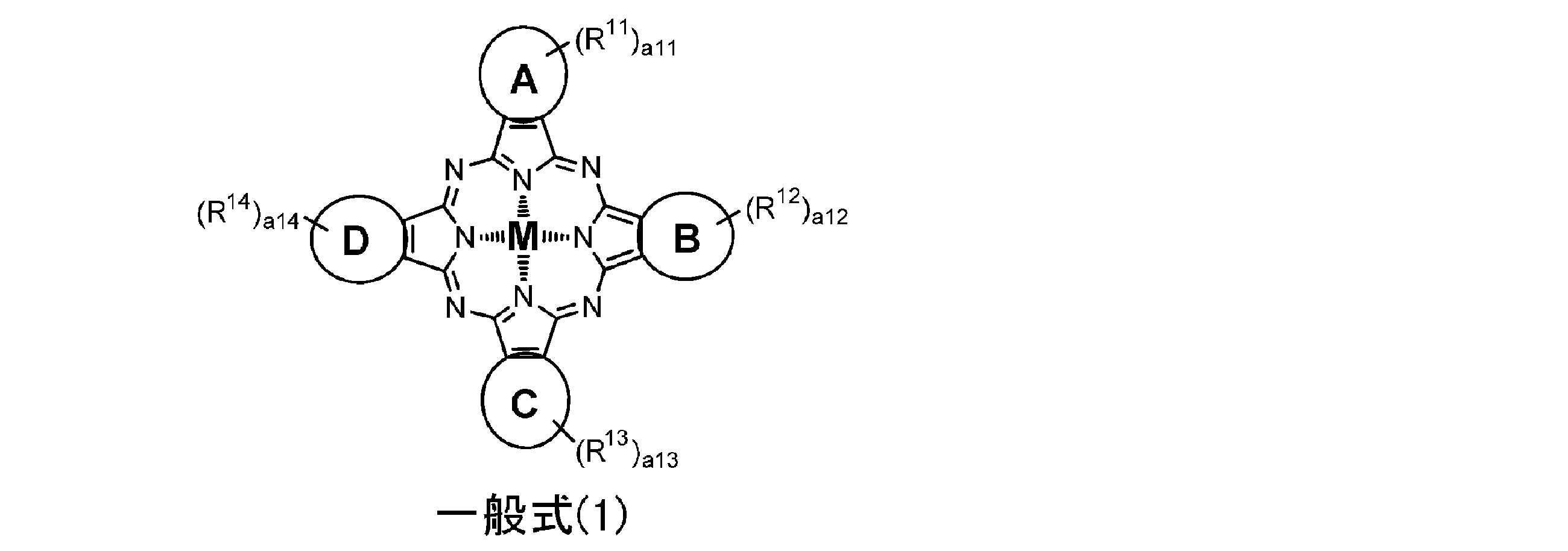
<2>一般式(1)において、前記A~Dの芳香環のうち、酸性基を有する芳香環が、π電子不足系ヘテロ芳香環、又はπ電子不足系ヘテロ芳香環が結合したベンゼン環若しくはナフタレン環である、前記<1>項記載の金属錯体色素。
<3>一般式(1)において、前記A~Dの芳香環のうち、酸性基を有する芳香環の数が、1つ又は2つであることを特徴とする、前記<1>又は<2>項記載の金属錯体色素。
<4>一般式(1)において、前記A~Dの芳香環のうち、酸性基を有さない芳香環が、それぞれ独立にベンゼン環、ナフタレン環、アントラセン環、フェナントレン環、チオフェン環、又はベンゾチオフェン環である、前記<1>~<3>のいずれか1項記載の金属錯体色素。
<5>一般式(1)において、前記酸性基がカルボキシル基であることを特徴とする前記<1>~<4>のいずれか1項記載の金属錯体色素。
<6>一般式(1)において、前記酸性基以外のR11~R14で表される置換基が、それぞれ独立に、アルキル基、アリール基、ヘテロ環基、アルキルオキシ基、アルキルチオ基、アルキルシリル基、アリールオキシ基、ヘテロアリールオキシ基、アリールチオ基、ヘテロアリールチオ基又はアリールシリル基、ヘテロアリールシリル基である、前記<1>~<5>のいずれか1項記載の金属錯体色素。
<7>一般式(1)において、a11~a14がそれぞれ独立に1~4の整数であることを特徴とする前記<1>~<6>のいずれか1項記載の金属錯体色素。
<8>一般式(1)において、Mが、銅、亜鉛、スズ、ニッケル、鉄、コバルト、ケイ素、パラジウム、クロロ-アルミニウム、マグネシウム、ガリウム、チタニルオキシ、又はバナジルオキシである、前記<1>~<7>のいずれか1項記載の金属錯体色素。
<9>一般式(1)で表される金属錯体色素が下記一般式(8)又は(9)で表される金属錯体色素である、前記<1>~<8>のいずれか1項記載の金属錯体色素。
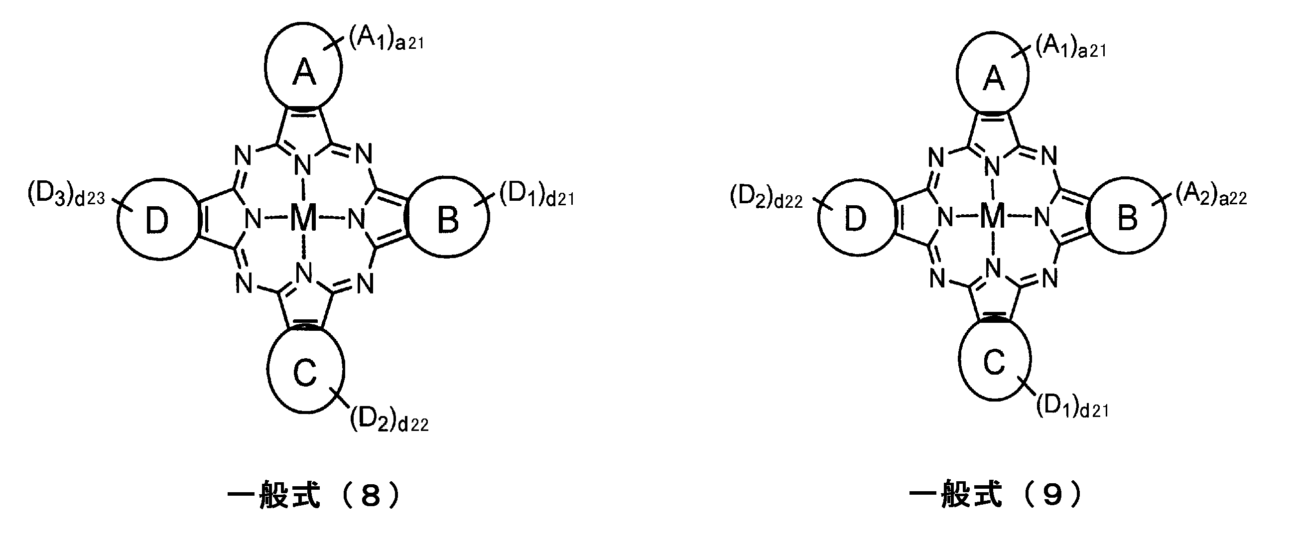
<10>前記<1>~<9>のいずれか1項記載の金属錯体色素からなる光電変換素子用色素。
<11>前記<1>~<9>のいずれか1項記載の金属錯体色素と半導体微粒子とを有する感光体層を具備した、光電変換素子。
<12>前記感光体層が、下記一般式(2)で表される金属錯体色素をさらに含む、前記<11>項記載の光電変換素子。
Mz(LL1)m1(LL2)m2(X)m3・CI 一般式(2)
[一般式(2)において、Mzは金属原子を表し、LL1は下記一般式(3)で表される2座又は3座の配位子を表し、LL2は下記一般式(4)で表される2座又は3座の配位子を表す。Xはアシルオキシ基、アシルチオ基、チオアシルオキシ基、チオアシルチオ基、アシルアミノオキシ基、チオカルバメート基、ジチオカルバメート基、チオカルボネート基、ジチオカルボネート基、トリチオカルボネート基、アシル基、チオシアネート基、イソチオシアネート基、シアネート基、イソシアネート基、シアノ基、アルキルチオ基、アリールチオ基、アルコキシ基及びアリールオキシ基からなる群から選ばれた基で配位する1座又は2座の配位子、又はハロゲン原子、カルボニル、ジアルキルケトン、1,3-ジケトン、カルボンアミド、チオカルボンアミド及びチオ尿素からなる群より選ばれる1座又は2座の配位子を表す。m1は0~3の整数を表し、m1が2以上のとき、LL1は同じでも異なっていてもよい。m2は1~3の整数を表し、m2が2以上のとき、LL2は同じでも異なっていてもよい。m3は0~3の整数を表し、m3が2以上のとき、Xは同じでも異なっていてもよく、X同士が連結していてもよい。CIは一般式(2)において、電荷を中和させるのに対イオンが必要な場合の対イオンを表す。


<13>導電性支持体上に、前記感光体層、電荷移動体及び対極をこの順序で積層した構造を有する、前記<11>又は<12>項記載の光電変換素子。
<14>前記金属錯体色素が前記半導体微粒子に吸着したことを特徴とする前記<11>~<13>のいずれか1項記載の光電変換素子。
<15>前記<11>~<14>のいずれか1項記載の光電変換素子を備えることを特徴とする光電気化学電池。
図1に示すように、光電変換素子10は、導電性支持体1、並びに、導電性支持体1上にその順序で配された、感光体層2、電荷移動体層3及び対極4からなる。前記導電性支持体1と感光体層2とにより受光電極5を構成している。その感光体層2は導電性微粒子22と増感色素21とを有しており、色素21はその少なくとも一部において導電性微粒子22に吸着している(色素は吸着平衡状態になっており、一部電荷移動体層に存在していてもよい)。感光体層2が形成された導電性支持体1は光電変換素子10において作用電極として機能する。この光電変換素子10を外部回路6で仕事をさせる電池用途に使用できるようにして、光電気化学電池100として作動させることができる。
なお、光電変換素子の上下は特に定めなくてもよいが、本明細書において、図示したものに基づいて言えば、受光側となる対極4の側を上部(天部)の方向とし、導電性支持体1の側を下部(底部)の方向とする。
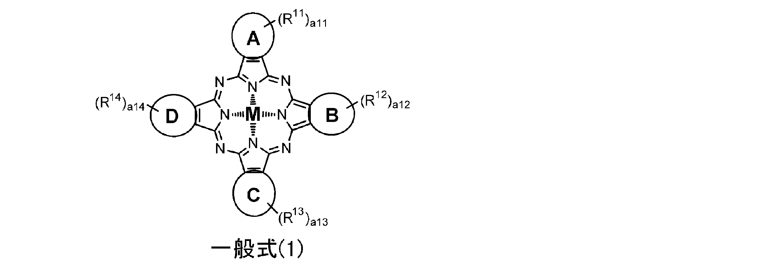
また、置換基が二つ以上ある場合は、同じでも異なってもよい。また、可能な場合には互いに連結して環を形成してもよい。
本発明において、前記酸性基としては、カルボキシル基、スルホン酸基、ホスホリル基又はホスホニル基が好ましく、カルボキシル基がより好ましい。
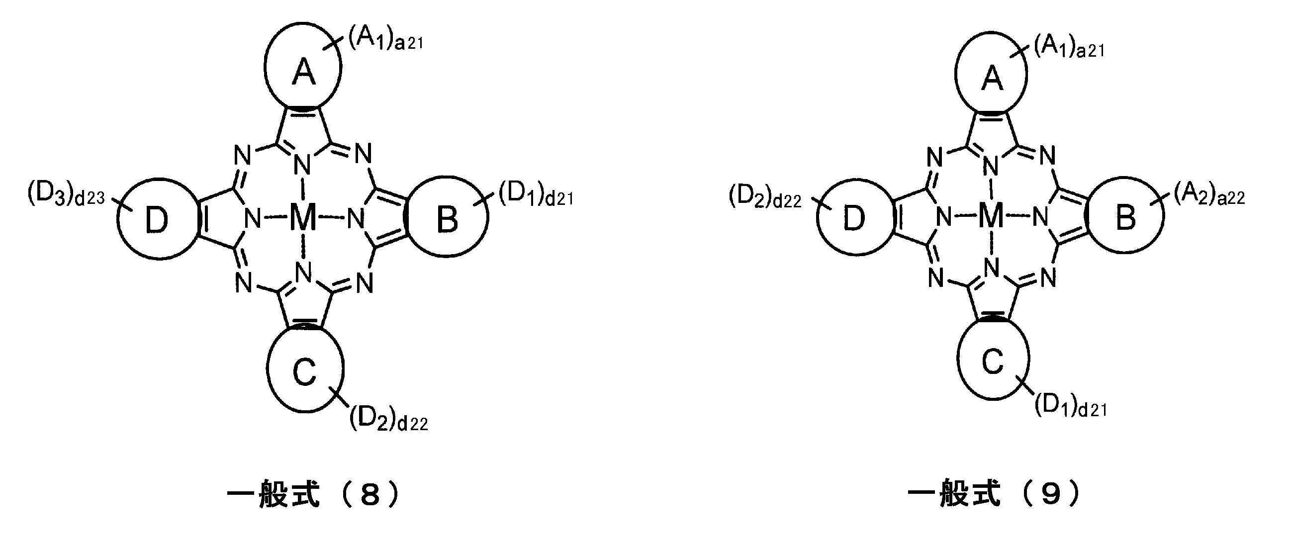
一般式(8)及び(9)において、A1及びA2は、それぞれ独立に酸性基を表し、それぞれ同一でも異なっていてもよい。酸性基の具体例としては、一般式(1)におけるR11~R14の酸性基として例示したものが挙げられ、好ましい範囲も同様である。
さらに、一般式(1)で表される色素の400nm以上の波長における光吸収波長域は、400~1500nmの範囲にあることが好ましく、400~1200nmの範囲にあることがより好ましい。また、Q帯のピークとSoret帯のピークとの波長差は、100~400nmの範囲にあることが好ましく、150~350nmの範囲にあることがより好ましい。


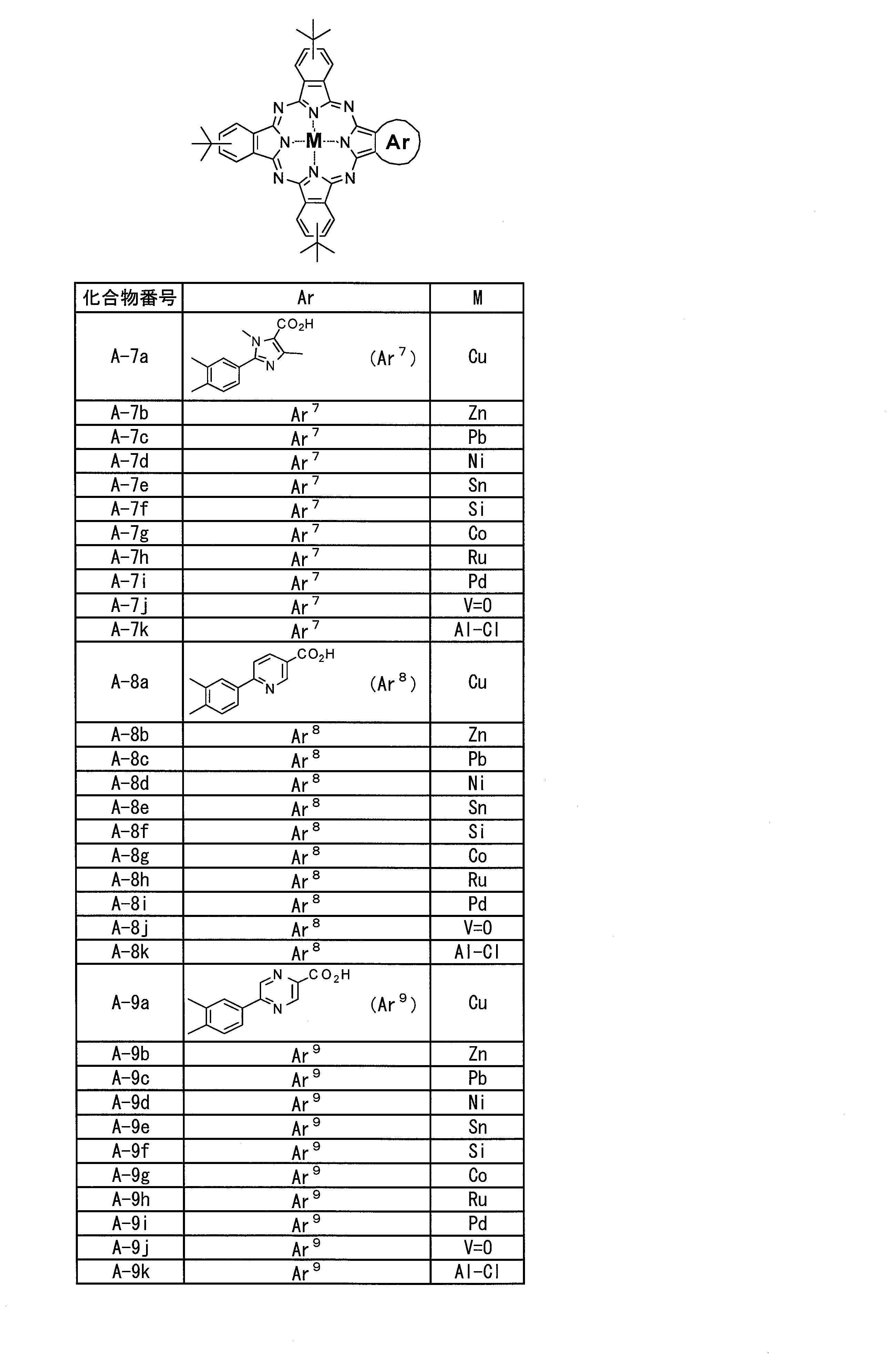

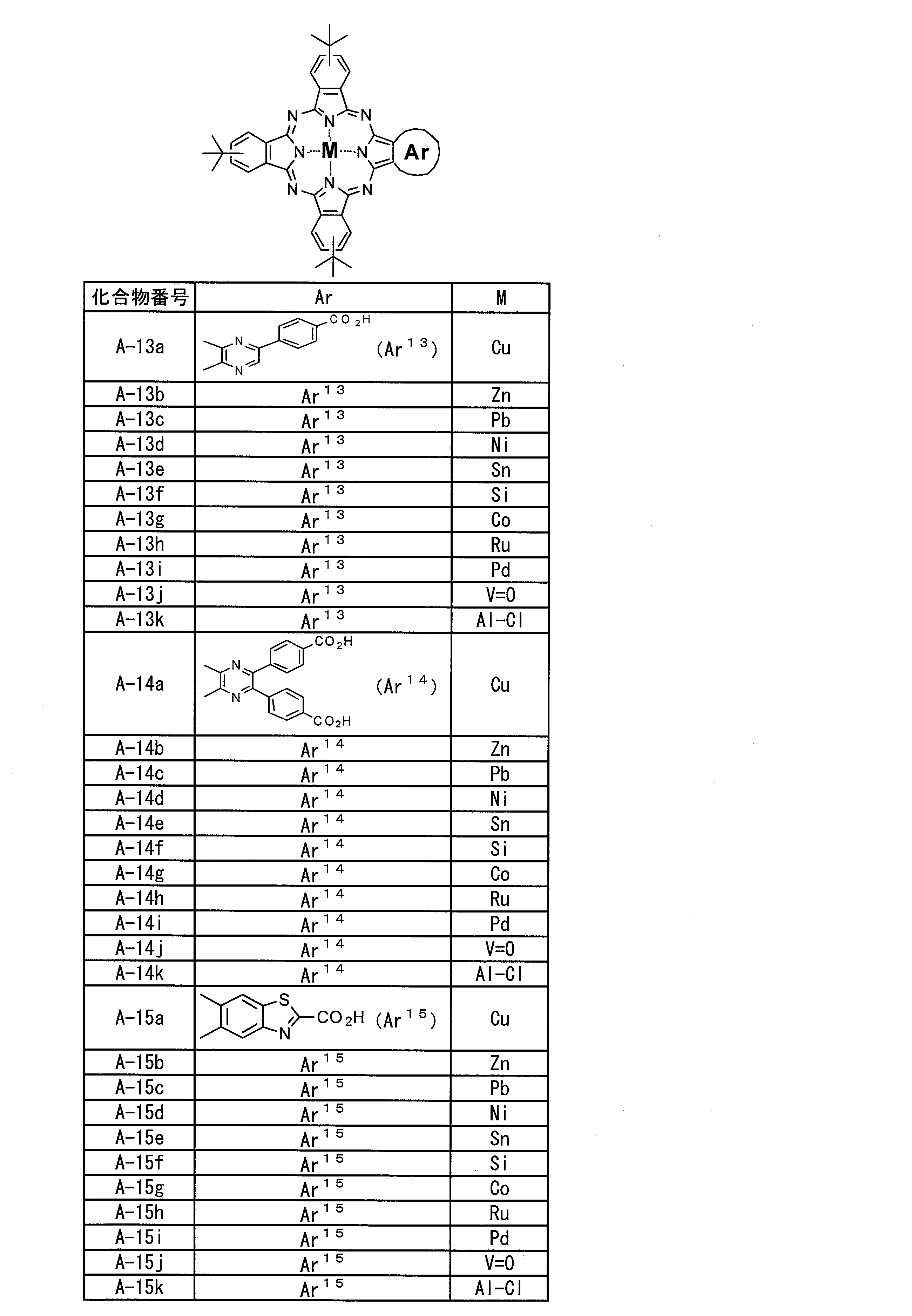

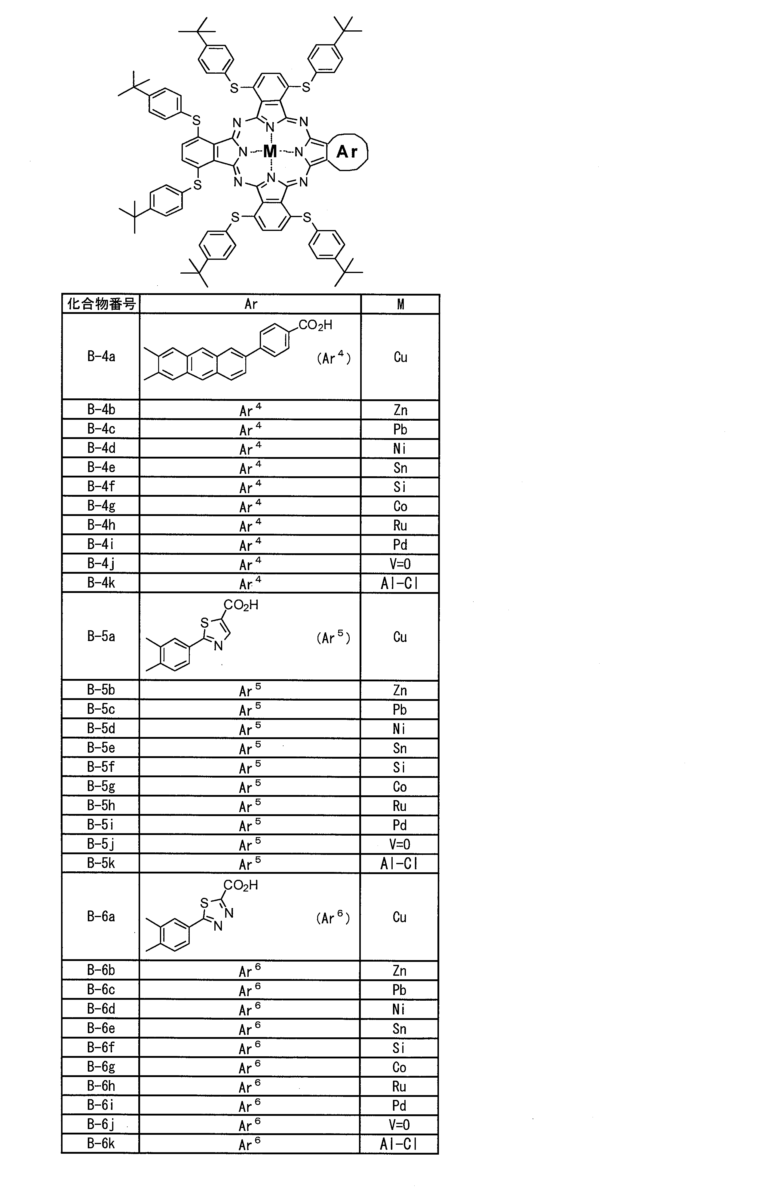


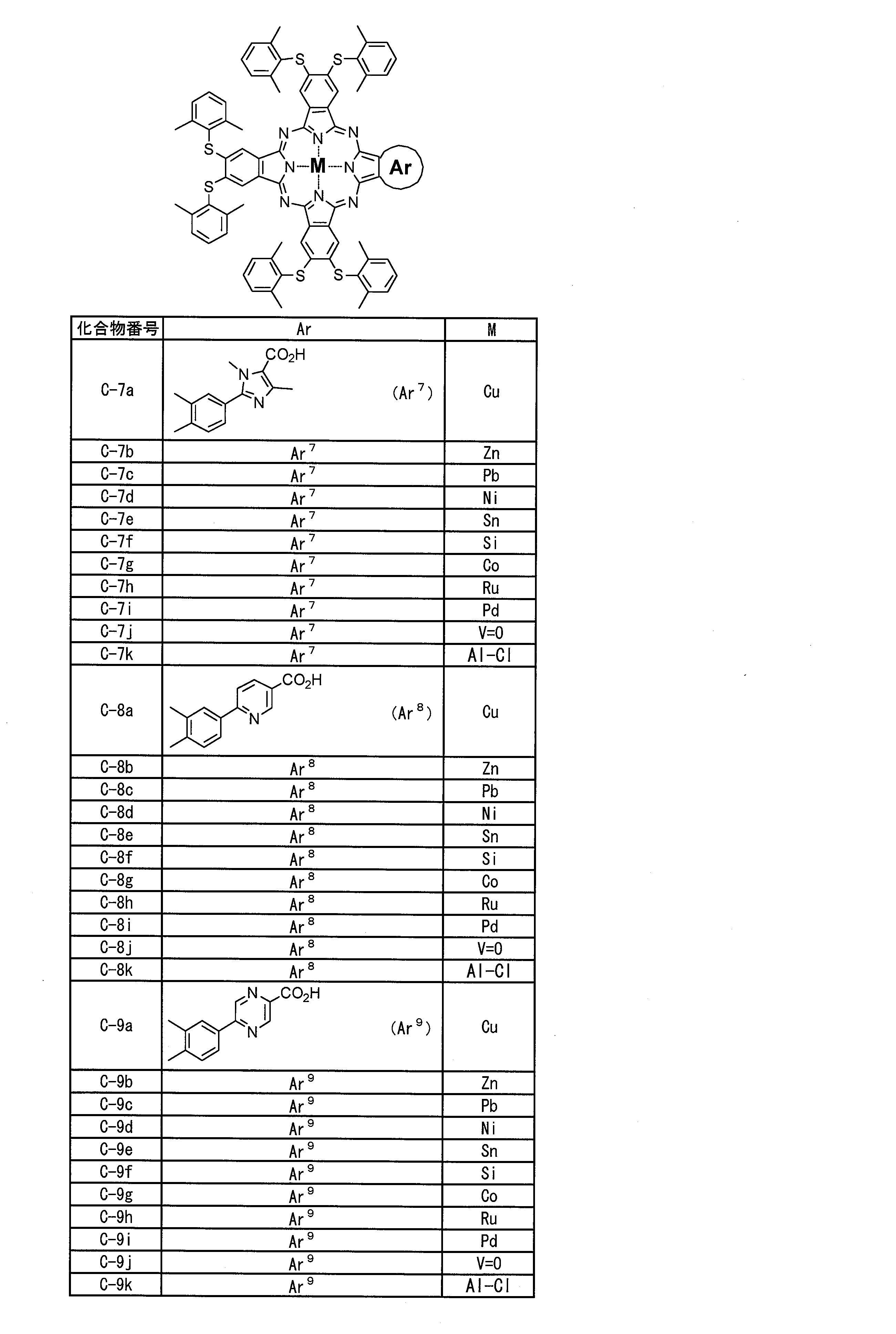
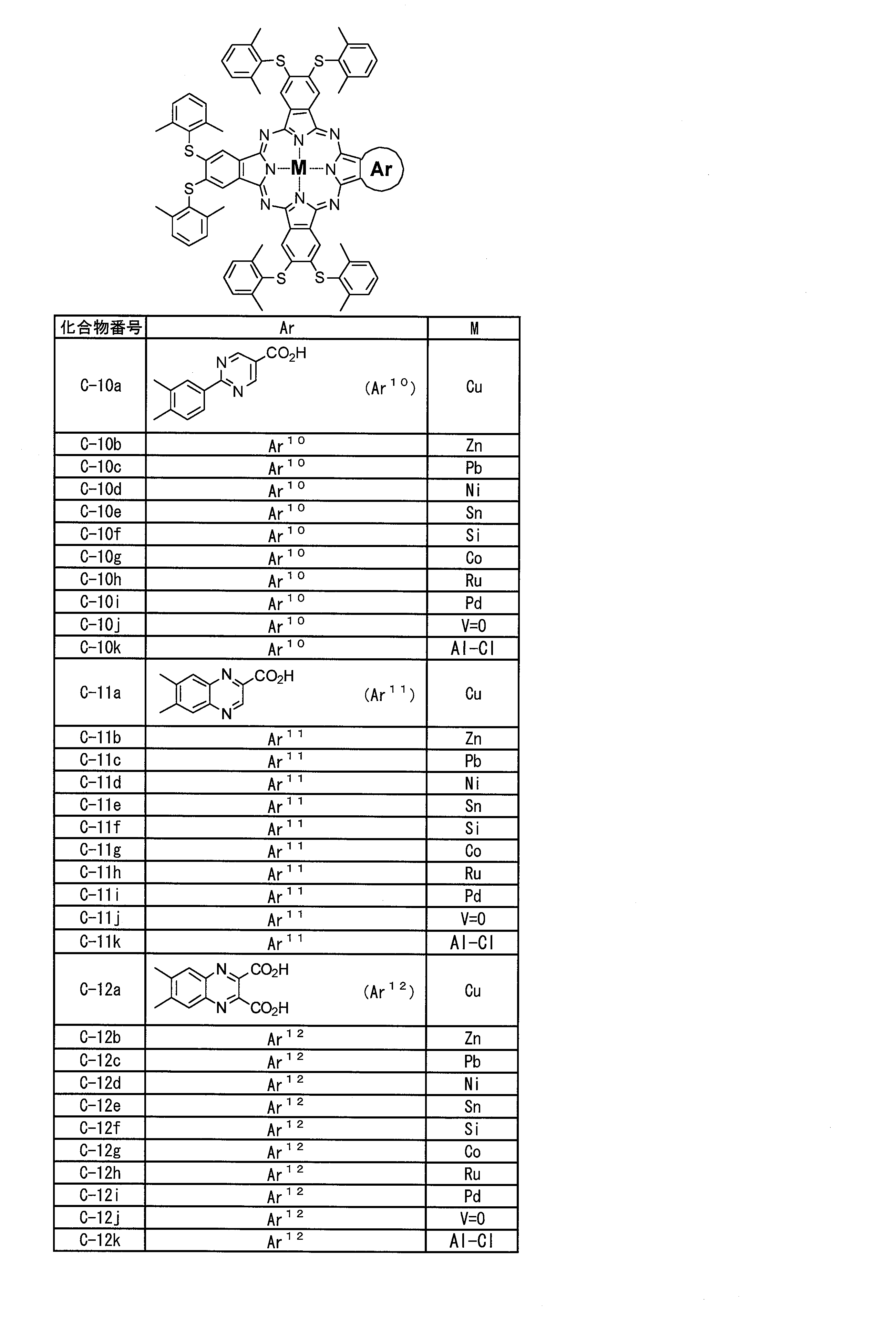

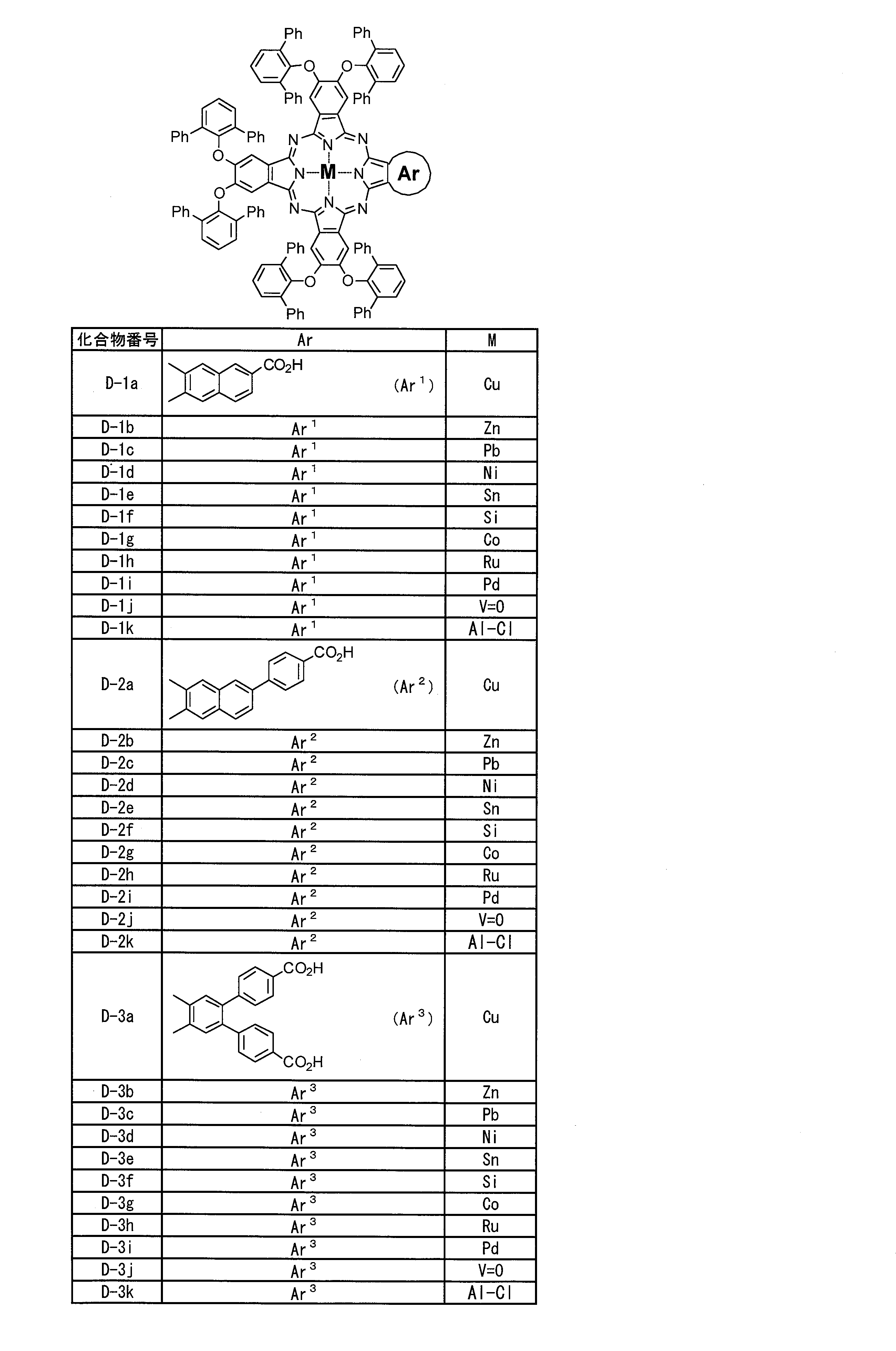

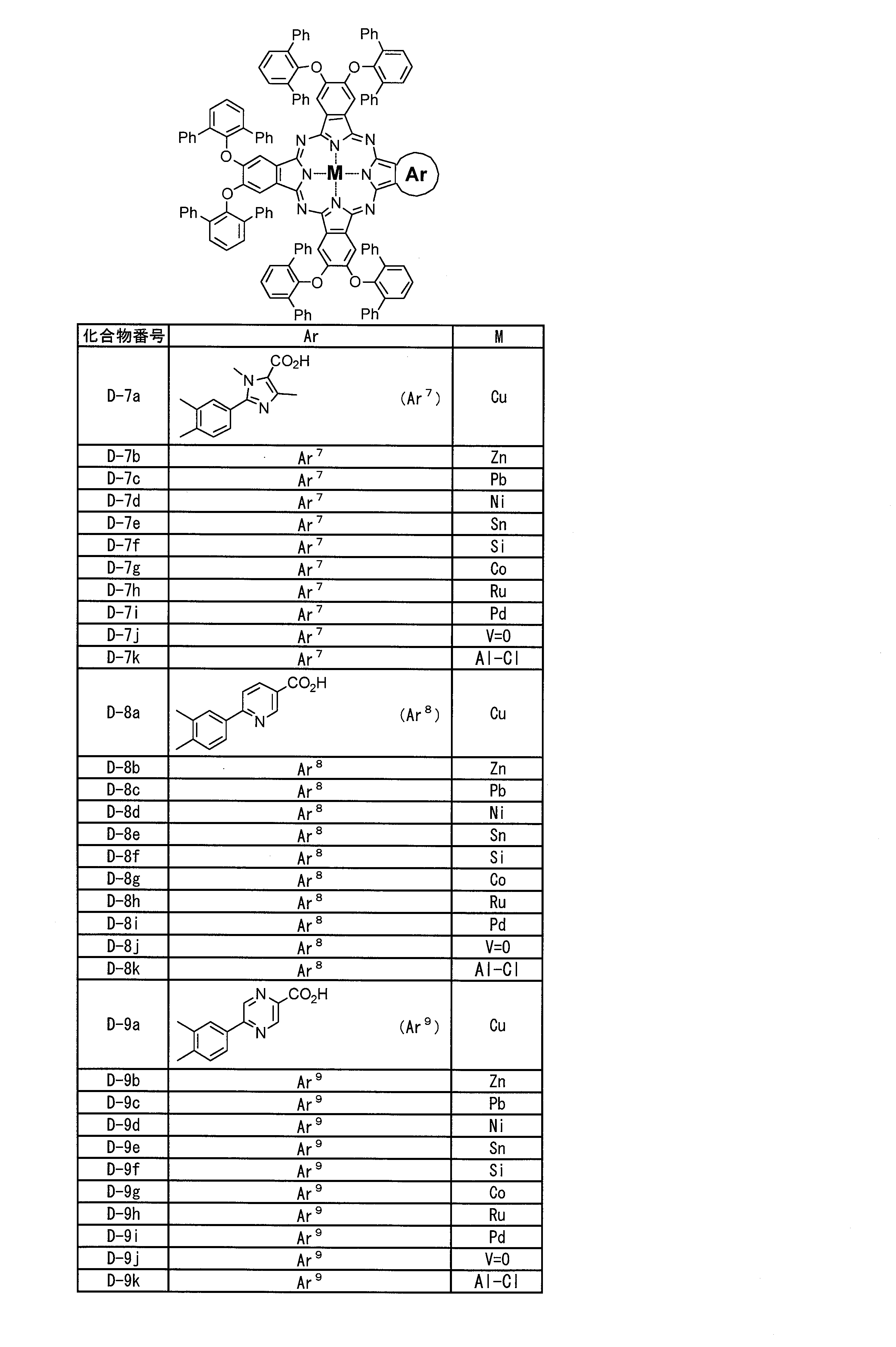
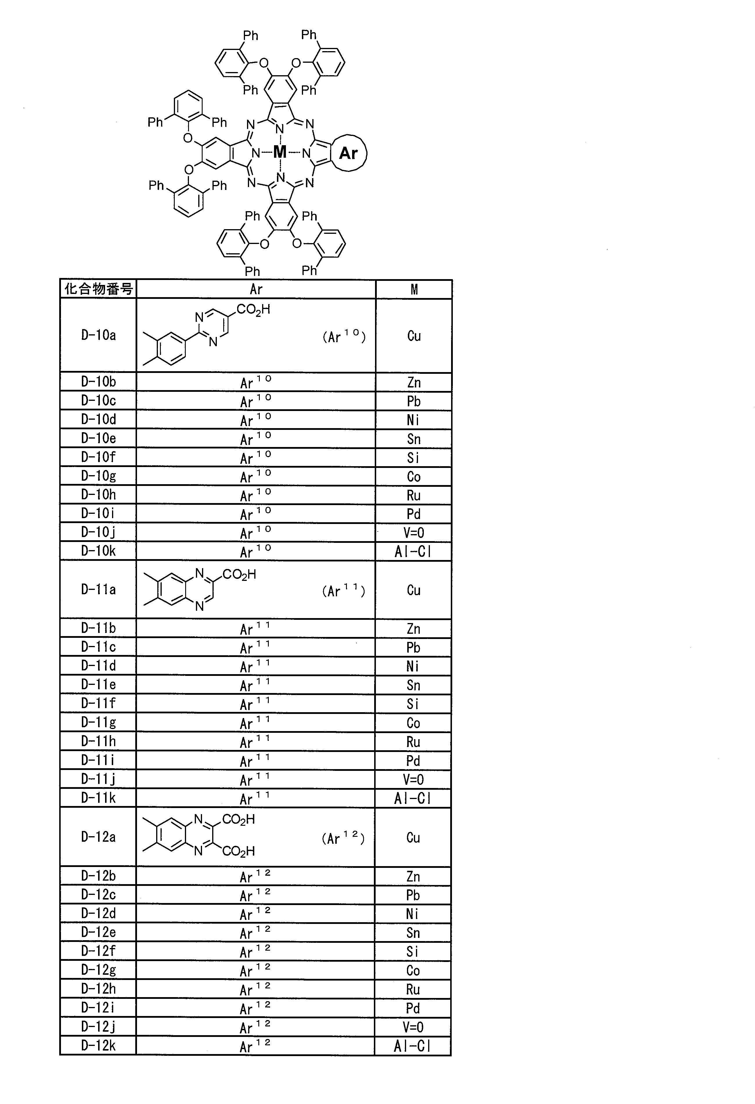
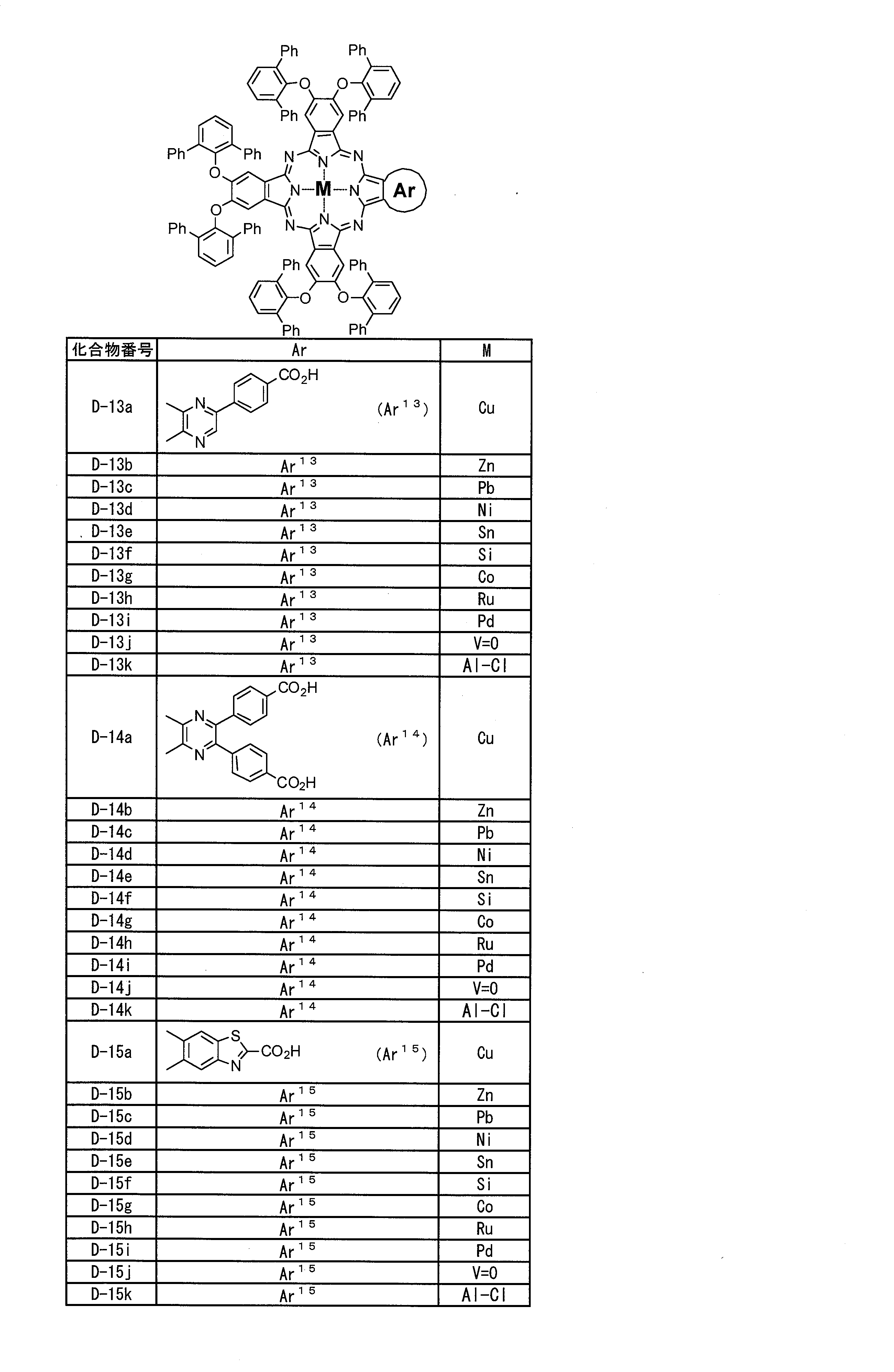
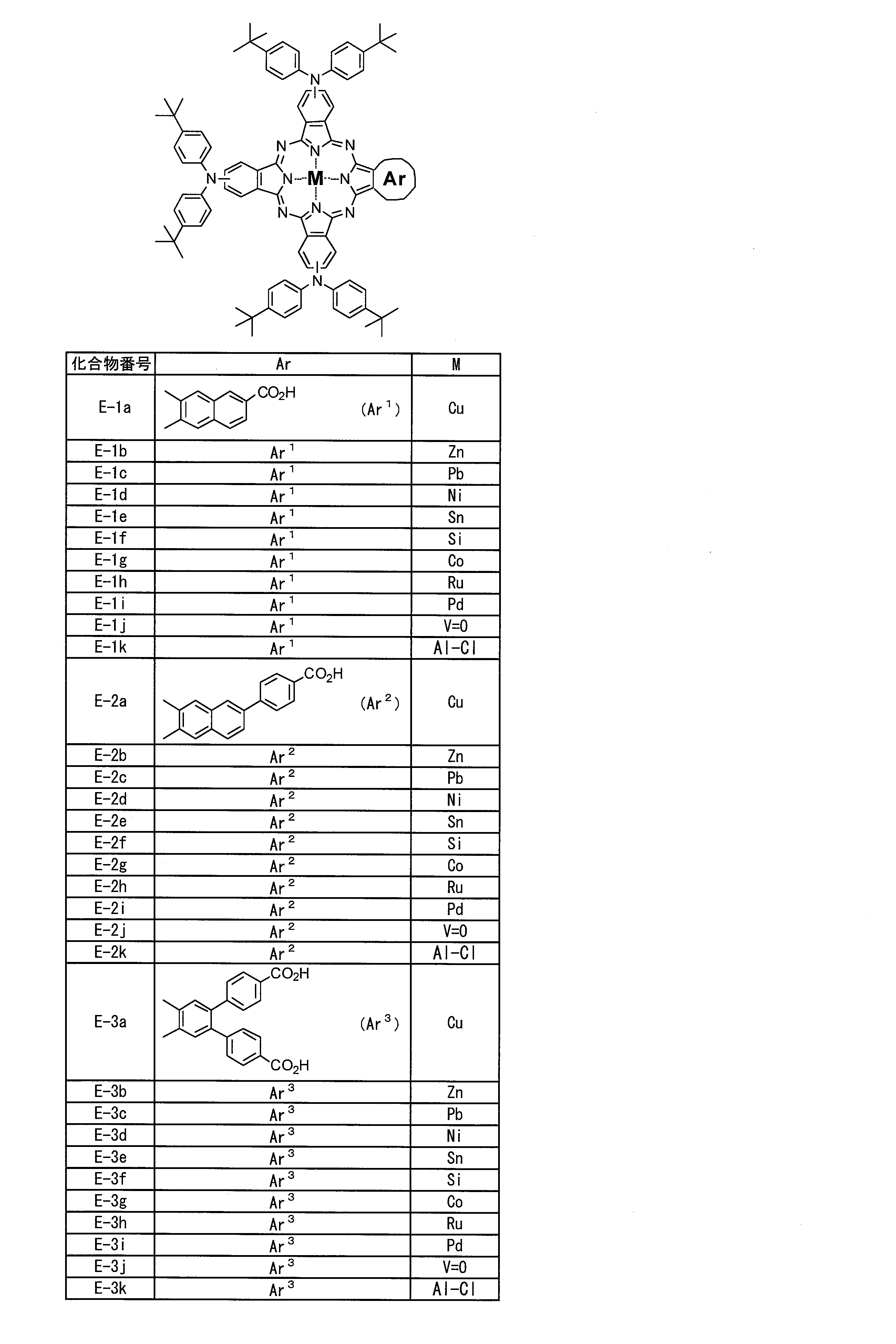

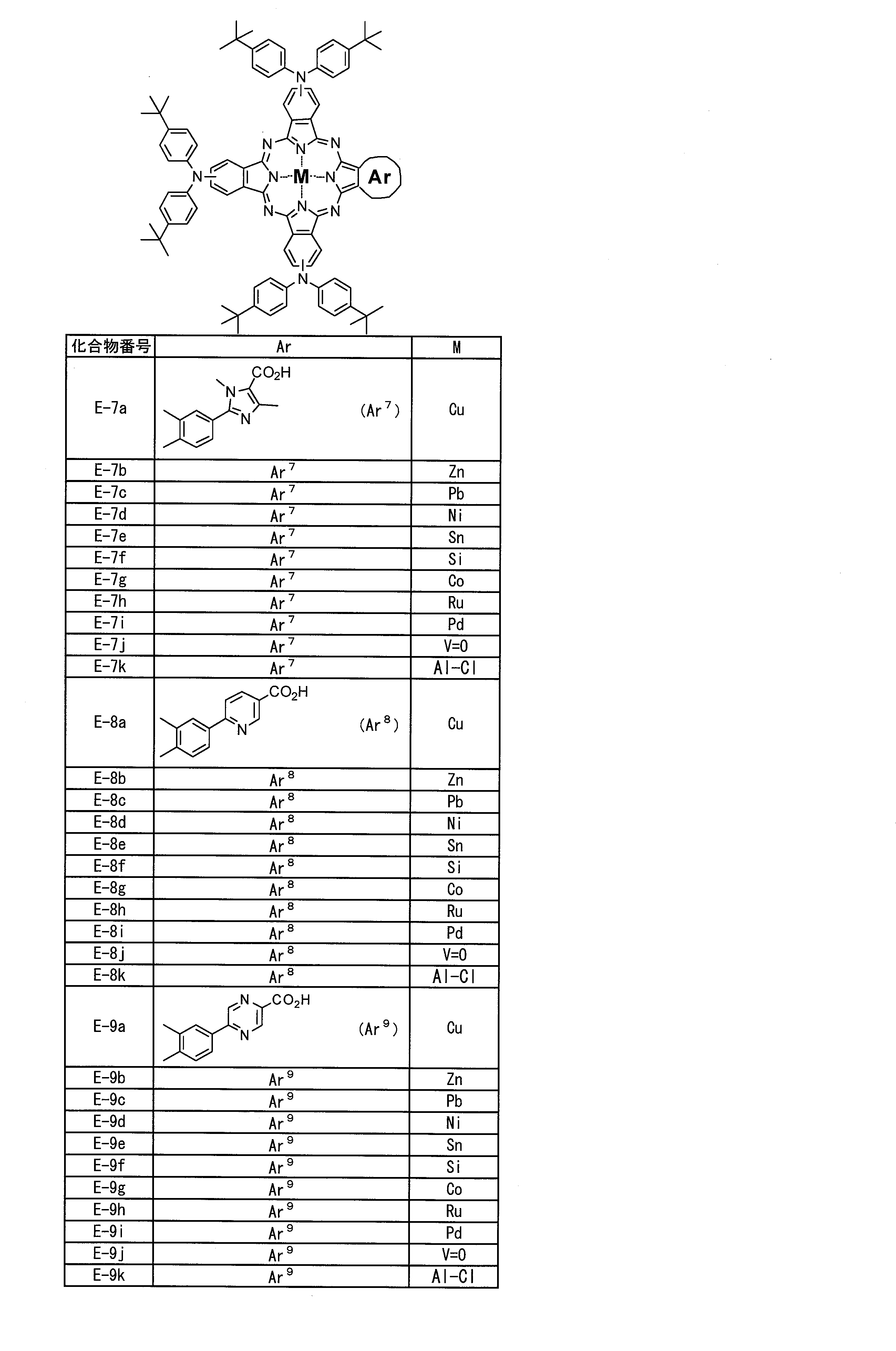
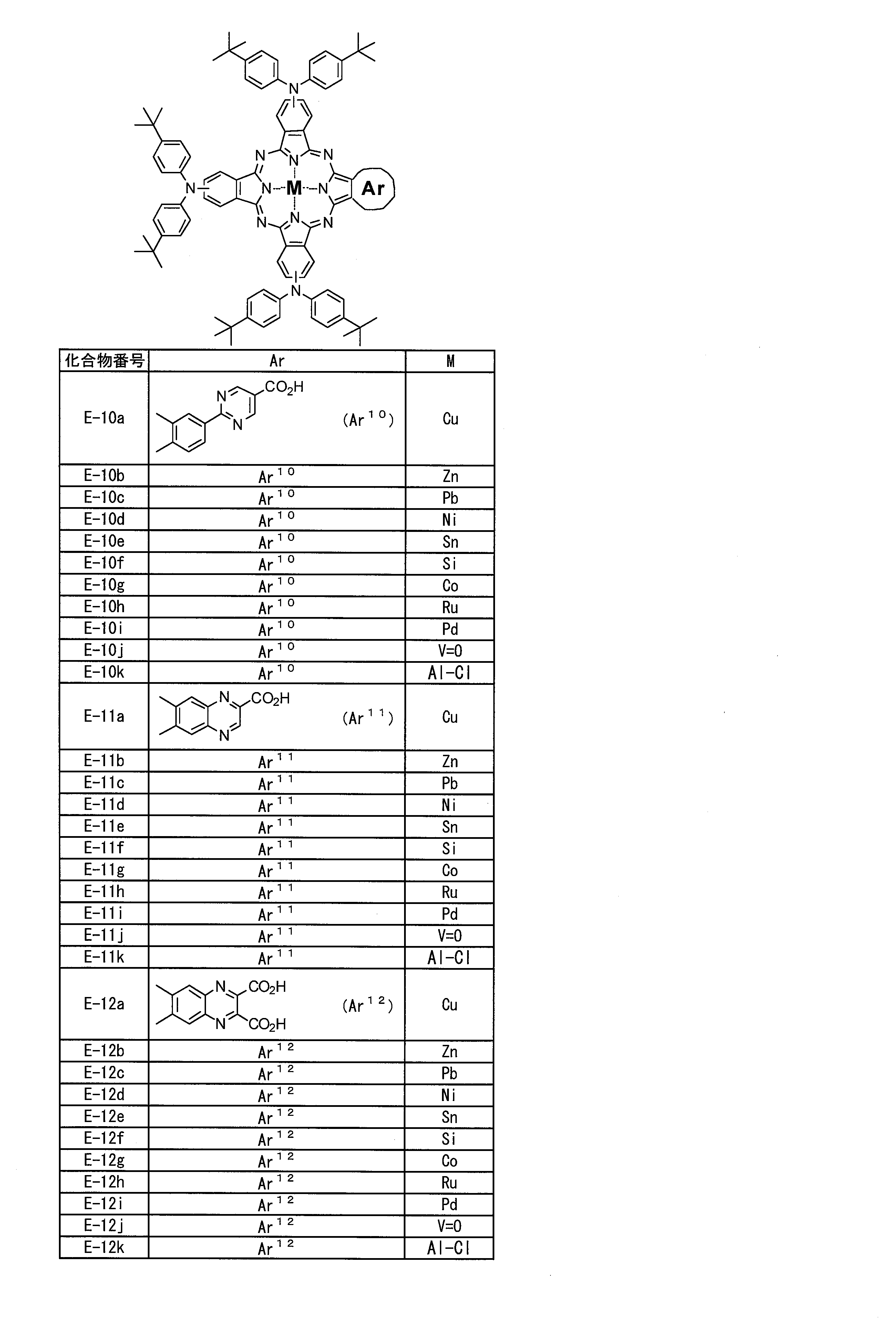
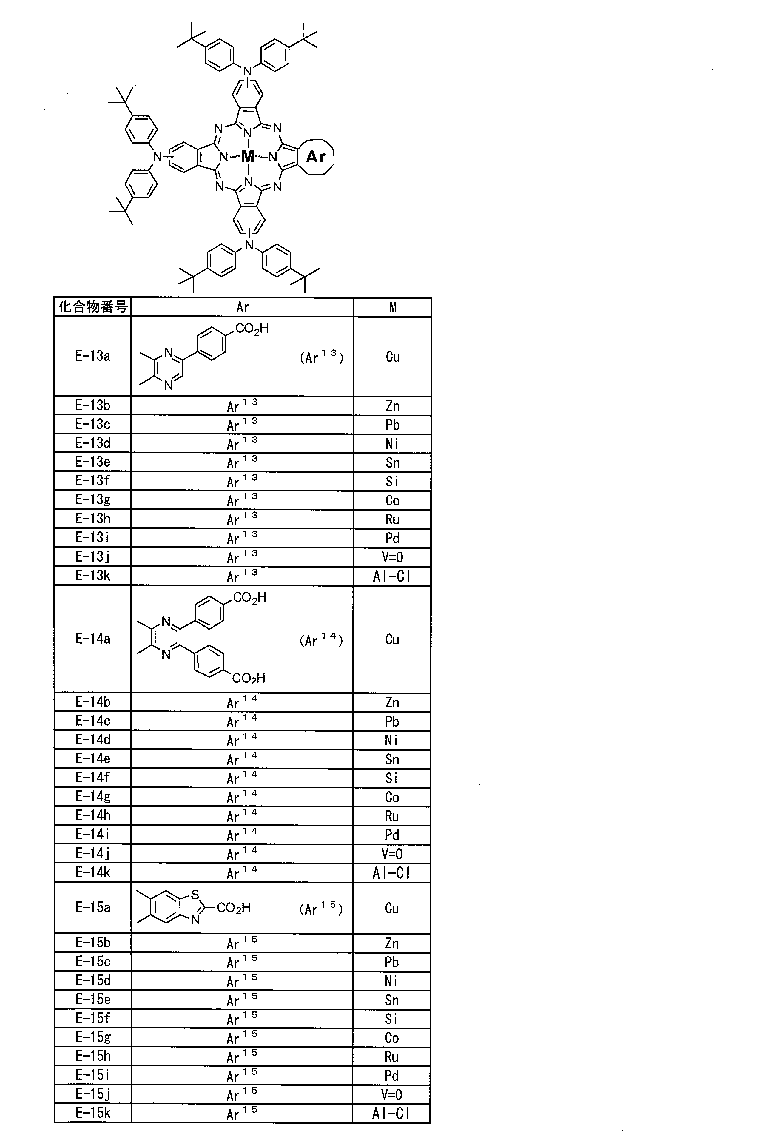
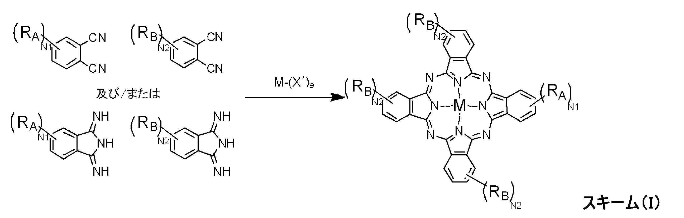
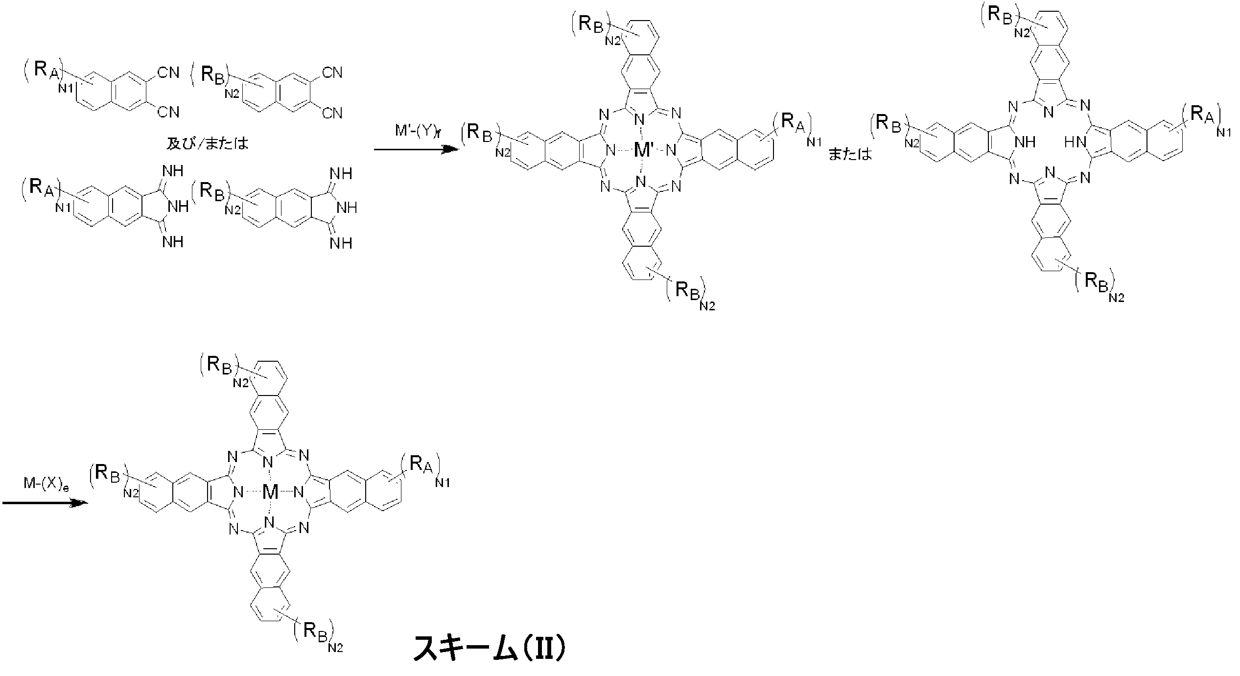
一般式(5) : M-(X’)e
一般式(5)中、Mは一般式(1)のMと同義である。X’はハロゲン原子、酢酸イオン、アセチルアセトネート、酸素などの1価又は2価の配位子を表し、eは1~4の整数を表す。
一般式(6) : M’-(Y)f
一般式(6)中、M’はアルカリ金属を表し、Yはハロゲン原子、酢酸イオン、アセチルアセトネート、アルコラート、酸素などの1価又は2価の配位子を表し、fは1~4の整数を表す。
溶媒の使用量に特に制限はないが、芳香族ジニトリル化合物及び/又はジイミノピロール化合物の1~100質量倍が好ましく、好ましくは3~20質量倍がより好ましい。
具体的には、保護基で保護された酸性基(エステル基)を有する芳香族ジニトリル化合物及び/又はジイミノピロール化合物を含む、2種以上の芳香族ジニトリル化合物及び/又はジイミノピロール化合物を前記一般式(5)で表される金属誘導体と反応させ、生成した中間体を下記一般式(7)で表されるアルカリ金属の水酸化物塩を用いて加水分解することにより、合成することができる。あるいは、保護基で保護された酸性基(エステル基)を有する芳香族ジニトリル化合物及び/又はジイミノピロール化合物を含む、2種以上の芳香族ジニトリル化合物及び/又はジイミノピロール誘導体を前記一般式(6)で表される金属誘導体と反応させた後に、前記一般式(5)で表される金属誘導体と反応させ、生成した中間体を下記一般式(7)で表されるアルカリ金属の水酸化物塩を用いて加水分解することによって合成することができる。
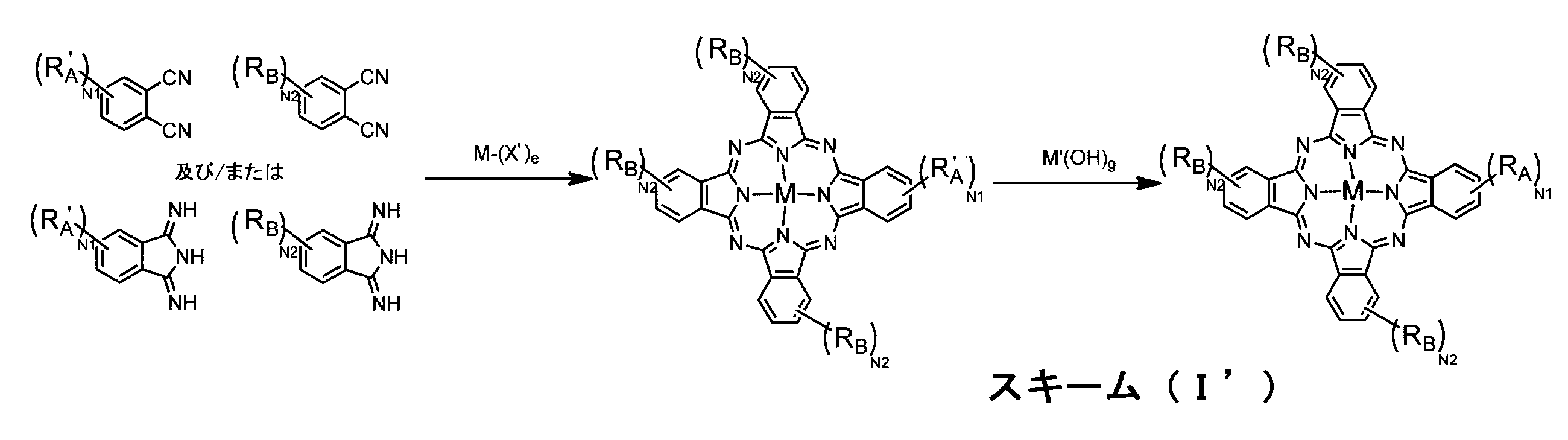

一般式(7) : M’(OH)g
一般式(7)中、M’はアルカリ金属を表し、gは1~2の整数を表す。
溶媒の使用量に特に制限はないが、芳香族ジニトリル化合物及び/又はジイミノピロール化合物の1~100質量倍が好ましく、3~60質量倍がより好ましい。
あるいは反応終了後、反応溶媒を留去してあるいは留去せずに、水又は氷にあけ、中和してあるいは中和せずに遊離した生成物を精製せずに、あるいは再結晶、カラムクロマトグラフィー、HPLC等にて精製する操作を単独に、あるいは組み合わせて行なった後、本発明の金属錯体色素を提供することができる。
またあるいは、反応終了後、反応溶媒を留去して、あるいは留去せずに、水又は氷にあけ中和して、あるいは中和せずに、有機溶媒/水溶液にて抽出した生成物を精製せずに、あるいは晶析、カラムクロマトグラフィー、HPLCにて精製する操作を単独あるいは組み合わせて行なった後、本発明の金属錯体色素を提供することができる。
なお、本明細書において化合物(錯体、色素を含む)の表示については、当該化合物そのもののほか、その塩、錯体(錯体以外のとき)、そのイオンを含む意味に用いる。また、所望の効果を奏する範囲で、所定の形態で修飾された化合物を含む意味である。また、本明細書において置換・無置換を明記していない置換基については、その基に任意の置換基を有していてもよい意味である。これは置換・無置換を明記していない化合物についても同義である。好ましい置換基としては、上述の置換基Tが挙げられる。
Mz(LL1)m1(LL2)m2(X)m3・CI 一般式(2)
一般式(2)の構造を有する色素は、金属原子に、配位子LL1及び/又は配位子LL2と、場合により特定の官能基Xが配位しており、必要な場合はCIにより電気的に中性に保たれている。

R25及びR26は、1~3個の電子供与基を有するヘテロ環基が好ましく、チエニルがより好ましい。該電子供与基はアルキル基、アルケニル基、アルキニル基、シクロアルキル基、アルコキシ基、アリールオキシ基、アミノ基、アシルアミノ基(以上好ましい例はR23及びR24の場合と同様)又はヒドロキシル基が好ましく、アルキル基、アルコキシ基、アミノ基又はヒドロキシル基であるのがより好ましく、アルキル基であるのが特に好ましい。R25及びR26は、は同じであっても異なっていてもよいが、同じであるのが好ましい。
ここで、L1及びL2はそれぞれ独立に、置換若しくは無置換のエテニレン基、置換若しくは無置換のエチニレン基及び置換若しくは無置換の2価のヘテロ環基からなる群から選ばれる少なくとも1つからなる共役鎖を表す。エテニレン基が置換基を有する場合、該置換基はアルキル基であるのが好ましく、メチル基であるのがより好ましい。
L1及びL2はそれぞれ独立に、炭素原子数2~6個の共役鎖であるのが好ましく、エテニレン、ブタジエニレン、エチニレン、ブタジイニレン、メチルエテニレン又はジメチルエテニレンがより好ましく、エテニレン又はブタジエニレンが特に好ましく、エテニレンが最も好ましい。L1とL2は同じであっても異なっていてもよいが、同じであるのが好ましい。なお、共役鎖が炭素―炭素二重結合を含む場合、各二重結合はトランス体であってもシス体であってもよく、これらの混合物であってもよい。
配位子LL1が酸性基を少なくとも1個有するときは、一般式(3)中のm1は2または3であるのが好ましく、2であるのがより好ましい。

前記酸性基は、Za、Zb又はZcが形成する環に直接結合していてもよいし、連結基を介してZa、Zb又はZcが形成する環に結合していてもよい。連結基としては特に制限はなく、メチレン基、エテニレン基、エチニレン基、アリーレン基、ヘテロアリーレン基、またはこれらの連結基を組合せた連結基等が挙げられる。
一般式(4)中、cは0又は1を表す。cは0が好ましい。
Xが1座配位子のとき、Xはチオシアネート基、イソチオシアネート基、シアネート基、イソシアネート基、シアノ基、アルキルチオ基及びアリールチオ基からなる群から選ばれる基で配位する配位子、又はハロゲン原子、カルボニル、ジアルキルケトン及びチオ尿素からなる群より選ばれる配位子であるのが好ましい。
置換基が解離性基を有することなどにより、一般式(2)で表される色素は解離して負電荷を持ってもよい。この場合、一般式(2)で表される色素全体の電荷はCIにより電気的に中性とされる。
対イオンCIが負の対イオンの場合、対イオンCIは、無機陰イオンでも有機陰イオンでもよい。例えば、ハロゲン陰イオン(例えば、フッ化物イオン、塩化物イオン、臭化物イオン、ヨウ化物イオン等)、置換アリールスルホン酸イオン(例えばp-トルエンスルホン酸イオン、p-クロロベンゼンスルホン酸イオン等)、アリールジスルホン酸イオン(例えば1,3-ベンゼンジスルホン酸イオン、1,5-ナフタレンジスルホン酸イオン、2,6-ナフタレンジスルホン酸イオン等)、アルキル硫酸イオン(例えばメチル硫酸イオン等)、硫酸イオン、チオシアン酸イオン、過塩素酸イオン、テトラフルオロホウ酸イオン、ヘキサフルオロホスフェートイオン、ピクリン酸イオン、酢酸イオン、トリフルオロメタンスルホン酸イオン等が挙げられる。さらに電荷均衡対イオンとして、イオン性ポリマーあるいは色素と逆電荷を有する他の色素を用いてもよく、金属錯イオン(例えばビスベンゼン-1,2-ジチオラトニッケル(III)等)も使用可能である。
(A1)pRu(B-a)(B-b)(B-c) 一般式(10)
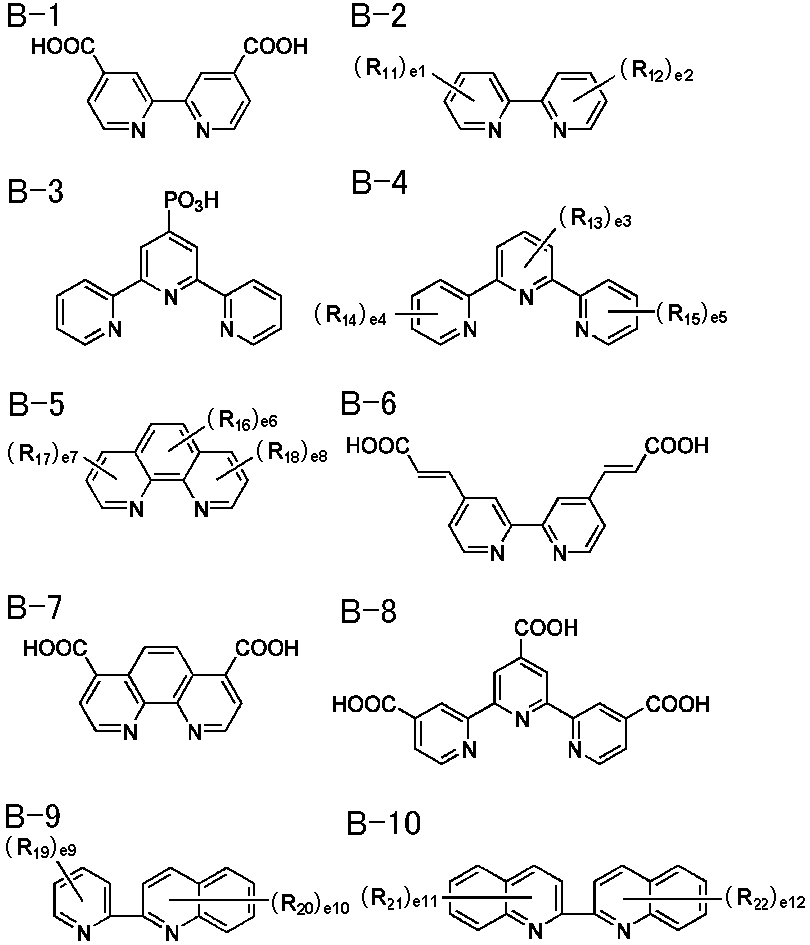
置換基としては、ハロゲン原子、炭素原子数1~12の置換又は無置換のアルキル基、アルキルオキシ基、炭素原子数2~20の置換又は無置換のアルケニル基、炭素原子数7~12の置換又は無置換のアラルキル基、アルキルオキシアリール基、炭素原子数6~12の置換又は無置換のアリール基、あるいは前述の酸性基(これらの酸性基は塩を形成していてもよい)が挙げられる。アルキル基及びアラルキル基のアルキル部分は直鎖状でも分岐状でもよい。また、アリール基およびアラルキル基のアリール部分は単環でも多環(縮合環、環集合)でもよい。R11~R22で表される置換基はさらに置換されていてもよく、さらに置換する置換基としてはR11~R22として挙げた置換基であり、酸性基で置換されていることが好ましい。R11~R22で表される置換基は、それ自身が酸性基であるか、または酸性基を置換基として有する基であることが好ましい。
e1~e12は0以上の整数を表す。具体的には、e1およびe2はそれぞれ独立に0~4の整数を表し、e3は0~3の整数を表し、e4およびe5はそれぞれ独立に0~4の整数を表し、e6は0~2の整数を表し、e7およびe8はそれぞれ独立に0~3の整数を表し、e9は0~4の整数を表し、e10~e12はそれぞれ独立に0~6の整数を表す。e1~e12が2以上のとき、R11~R22はそれぞれ同じでも異なっていてもよい。e1~e12はそれぞれ独立に1である場合が好ましい。
R11とR12は同じでも異なっていてもよいが、同じであるのが好ましい。R13~R15は同じでも異なっていても良いが、同じであるのが好ましい。R16~R18は同じでも異なっていても良いが、同じであるのが好ましい。R19とR20は同じでも異なっていても良いが、同じであるのが好ましい。R21とR22は同じでも異なっていても良いが、同じであるのが好ましい。
B-a、B-bおよびB-cは同一でも異なっていてもよい。ただし、一般式(10)で表される化合物において、少なくとも1つの酸性基を有する。


一般式(2)の構造を有する色素は、溶液における極大吸収波長が、好ましくは300~700nmの範囲であり、より好ましくは400~650nmの範囲であり、特に好ましくは500~600nmの範囲である。
さらに、一般式(2)で表される色素の光吸収波長域は、300~900nmの範囲にあることが好ましく、350~850nmの範囲にあることがより好ましい。
図1に示すような本発明の光電変換素子の好ましい実施態様において、光電変換素子に用いられる電荷移動体層3には、電解質組成物からなる層が適用できる。その酸化還元対として、例えばヨウ素とヨウ化物(例えばヨウ化リチウム、ヨウ化テトラブチルアンモニウム、ヨウ化テトラプロピルアンモニウム等)との組み合わせ、アルキルビオローゲン(例えばメチルビオローゲンクロリド、ヘキシルビオローゲンブロミド、ベンジルビオローゲンテトラフルオロボレート)とその還元体との組み合わせ、ポリヒドロキシベンゼン類(例えばハイドロキノン、ナフトハイドロキノン等)とその酸化体との組み合わせ、2価と3価の鉄錯体(例えば赤血塩と黄血塩)の組み合わせ等が挙げられる。これらのうちヨウ素とヨウ化物との組み合わせが好ましい。
ヨウ素塩のカチオンは5員環又は6員環の含窒素芳香族カチオンであるのが好ましい。特に、一般式(1)で表される化合物及び一般式(2)で表される化合物のいずれも又は一方がヨウ素塩でない場合は、WO95/18456号、特開平8-259543号、電気化学,第65巻,11号,923頁(1997年)等に記載されているピリジニウム塩、イミダゾリウム塩、トリアゾリウム塩等のヨウ素塩を併用するのが好ましい。
本発明の光電変換素子に使用される電解質組成物中には、ヘテロ環4級塩化合物と共にヨウ素を含有するのが好ましい。ヨウ素の含有量は電解質組成物全体に対して0.1~20質量%であるのが好ましく、0.5~5質量%であるのがより好ましい。
溶媒としては低粘度でイオン移動度が高いか、高誘電率で有効キャリアー濃度を高めることができるか、あるいはその両方であるために優れたイオン伝導性を発現できるものが好ましい。このような溶媒としてカーボネート化合物(エチレンカーボネート、プロピレンカーボネート等)、複素環化合物(3-メチル-2-オキサゾリジノン等)、エーテル化合物(ジオキサン、ジエチルエーテル等)、鎖状エーテル類(エチレングリコールジアルキルエーテル、プロピレングリコールジアルキルエーテル、ポリエチレングリコールジアルキルエーテル、ポリプロピレングリコールジアルキルエーテル等)、アルコール類(メタノール、エタノール、エチレングリコールモノアルキルエーテル、プロピレングリコールモノアルキルエーテル、ポリエチレングリコールモノアルキルエーテル、ポリプロピレングリコールモノアルキルエーテル等)、多価アルコール類(エチレングリコール、プロピレングリコール、ポリエチレングリコール、ポリプロピレングリコール、グリセリン等)、ニトリル化合物(アセトニトリル、グルタロジニトリル、メトキシアセトニトリル、プロピオニトリル、ベンゾニトリル、ビスシアノエチルエーテル等)、エステル類(カルボン酸エステル、リン酸エステル、ホスホン酸エステル等)、非プロトン性極性溶媒(ジメチルスルホキシド(DMSO)、スルフォラン等)、水、特開2002-110262記載の含水電解液、特開2000-36332号公報、特開2000-243134号公報、及び再公表WO/00-54361号公報記載の電解質溶媒などが挙げられる。これらの溶媒は二種以上を混合して用いてもよい。
ゲル電解質に占めるモノマーの重量組成範囲は0.5~70質量%であるのが好ましい。より好ましくは1.0~50質量%である。ポリマーの架橋反応により電解質組成物をゲル化させる場合は、組成物に架橋可能な反応性基を有するポリマー及び架橋剤を添加するのが好ましい。好ましい反応性基はピリジン環、イミダゾール環、チアゾール環、オキサゾール環、トリアゾール環、モルホリン環、ピペリジン環、ピペラジン環等の含窒素複素環であり、好ましい架橋剤は窒素原子が求核攻撃できる官能基を2つ以上有する化合物(求電子剤)であり、例えば2官能以上のハロゲン化アルキル、ハロゲン化アラルキル、スルホン酸エステル、酸無水物、酸クロライド、イソシアネート等である。
本発明の光電変換素子に設けることができる伝導層は、導電性のよいものであれば特に限定されないが、例えば無機導電性材料、有機導電性材料、導電性ポリマー、分子間電荷移動錯体等が挙げられる。中でも分子間電荷移動錯体が好ましい。ここで、分子間電荷移動錯体は、ドナー材料とアクセプター材料とから形成されるものである。また、有機ドナーと有機アクセプターを好ましく用いることができる。
なお、伝導層の厚みは、特に限定されないが、多孔質を完全に埋めることができる程度が好ましい。
図1に示すような本発明の光電変換素子の好ましい実施態様において、導電性支持体1上には多孔質の半導体微粒子22に増感色素21が吸着された感光体層2が形成されている。後述する通り、例えば、半導体微粒子の分散液を導電性支持体に塗布・乾燥後、本発明の色素溶液に浸漬することにより、感光体層2を製造することができる。
導電性支持体としては、金属のように支持体そのものに導電性があるものか、又は表面に導電膜層を有するガラスや高分子材料を使用することができる。導電性支持体は実質的に透明であることが好ましい。実質的に透明であるとは光の透過率が10%以上であることを意味し、50%以上であることが好ましく、80%以上が特に好ましい。導電性支持体としては、ガラスや高分子材料に導電性の金属酸化物を塗設したものを使用することができる。このときの導電性の金属酸化物の塗布量は、ガラスや高分子材料の支持体1m2当たり、0.1~100gが好ましい。透明導電性支持体を用いる場合、光は支持体側から入射させることが好ましい。好ましく使用される高分子材料の一例として、テトラアセチルセルロース(TAC)、ポリエチレンテレフタレート(PET)、ポリエチレンナフタレート(PEN)、シンジオタクチックポリスチレン(SPS)、ポリフェニレンスルフィド(PPS)、ポリカーボネート(PC)、ポリアリレート(PAR)、ポリスルフォン(PSF)、ポリエステルスルフォン(PES)、ポリエーテルイミド(PEI)、環状ポリオレフィン、ブロム化フェノキシ等を挙げることができる。導電性支持体上には、表面に光マネージメント機能を施してもよく、例えば、特開2003-123859記載の高屈折膜及び低屈折率の酸化物膜を交互に積層した反射防止膜、特開2002-260746記載のライトガイド機能が挙げられる。
この他にも、金属支持体も好ましく使用することができる。その一例としては、チタン、アルミニウム、銅、ニッケル、鉄、ステンレスを挙げることができる。これらの金属は合金であってもよい。さらに好ましくは、チタン、アルミニウム、銅が好ましく、特に好ましくは、チタンやアルミニウムである。
導電性支持体上には、さらに特開平11-250944号公報等に記載の機能を付与してもよい。
導電膜層の厚さは0.01~30μmであることが好ましく、0.03~25μmであることが更に好ましく、特に好ましくは0.05~20μmである。
また、透明電極と多孔質半導体電極光触媒含有層を設けてもよい。透明導電層は積層構造でも良く、好ましい方法としてたとえば、ITO上にFTOを積層することができる。
図1に示すように、本発明の光電変換素子の好ましい実施態様において、導電性支持体1上には多孔質の半導体微粒子22に色素21が吸着された感光体層2が形成されている。後述する通り、例えば、半導体微粒子の分散液を前記の導電性支持体に塗布・乾燥後、本発明の色素溶液に浸漬することにより、感光体層2を製造することができる。
チタニアナノチューブ・ナノワイヤー・ナノロッドをチタニア微粒子に混合してもよい。
本発明においては、半導体微粒子以外の固形分の含量が、半導体微粒子分散液全体の10質量%以下よりなる半導体微粒子分散液を前記の導電性支持体に塗布し、適度に加熱することにより、多孔質半導体微粒子塗布層(感光体層)を得ることができる。
半導体微粒子分散液を作製する方法としては、前述のゾル・ゲル法の他に、半導体を合成する際に溶媒中で微粒子として析出させそのまま使用する方法、微粒子に超音波などを照射して超微粒子に粉砕する方法、あるいはミルや乳鉢などを使って機械的に粉砕しすり潰す方法、等が挙げられる。分散溶媒としては、水及び/又は各種の有機溶媒を用いることができる。有機溶媒としては、メタノール、エタノール、イソプロピルアルコール、シトロネロール、ターピネオールなどのアルコール類、アセトンなどのケトン類、酢酸エチルなどのエステル類、ジクロロメタン、アセトニトリル等が挙げられる。
半導体微粒子分散液の粘度が高すぎると分散液が凝集してしまい製膜することができず、逆に半導体微粒子分散液の粘度が低すぎると液が流れてしまい製膜することができないことがある。したがって分散液の粘度は、25℃で10~300N・s/m2が好ましい。さらに好ましくは、25℃で50~200N・s/m2である。
また、加熱処理に加えて光のエネルギーを用いることもできる。例えば、半導体微粒子として酸化チタンを用いた場合に、紫外光のような半導体微粒子が吸収する光を与えることで表面を活性化してもよいし、レーザー光などで半導体微粒子表面のみを活性化することができる。半導体微粒子に対して該微粒子が吸収する光を照射することで、粒子表面に吸着した不純物が粒子表面の活性化によって分解され、上記の目的のために好ましい状態とすることができる。加熱処理と紫外光を組み合わせる場合は、半導体微粒子に対して該微粒子が吸収する光を照射しながら、加熱が100℃以上250℃以下あるいは好ましくは100℃以上150℃以下で行われることが好ましい。このように、半導体微粒子を光励起することによって、微粒子層内に混入した不純物を光分解により洗浄するとともに、微粒子の間の物理的接合を強めることができる。
塗布後に圧力をかけても良く、圧力をかける方法としては、特表2003-500857号公報に記載の方法等が挙げられる。光照射の例としては、特開2001-357896号公報に記載の方法等が挙げられる。プラズマ・マイクロ波・通電の例としては、特開2002-353453号公報に記載の方法等が挙げられる。化学的処理としては、例えば特開2001-357896号公報に記載の方法が挙げられる。
前駆体として例えば、(NH4)2TiF6、過酸化チタン、金属アルコキシド・金属錯体・金属有機酸塩等が挙げられる。
また、金属有機酸化物(アルコキシドなど)を共存させたスラリーを塗布し加熱処理、光処理などで半導体膜を形成する方法、無機系前駆体を共存させたスラリー、スラリーのpHと分散させたチタニア粒子の性状を特定した方法が挙げられる。これらスラリーには、少量であればバインダーを添加しても良く、バインダーとしては、セルロース、フッ素ポリマー、架橋ゴム、ポリブチルチタネート、カルボキシメチルセルロースなどが挙げられる。
半導体微粒子又はその前駆体層の形成に関する技術としては、コロナ放電、プラズマ、UVなどの物理的な方法で親水化する方法、アルカリやポリエチレンジオキシチオフェンとポリスチレンスルホン酸などによる化学処理、ポリアニリンなどの接合用中間膜の形成などが挙げられる。
(2)乾式法として好ましくは、特開2000-231943号公報等が挙げられる。
(3)その他の方法として、好ましくは、特開2002-134435号公報等が挙げられる。
また、耐熱基板上でいったん塗膜を作製した後、プラスチック等のフィルムに転写する方法を用いても良い。好ましくは、特開2002-184475号公報記載のEVAを介して転写する方法、特開2003-98977号公報記載の紫外線、水系溶媒で除去可能な無機塩を含む犠牲基板上に半導体層・導電層を形成後、有機基板に転写後、犠牲基板を除去する方法などが挙げられる。
支持体として高分子材料を用いる場合、250℃以下で製膜後加熱することが好ましい。その場合の製膜方法としては、(1)湿式法、(2)乾式法、(3)電気泳動法(電析法を含む)の何れでも良く、好ましくは、(1)湿式法、又は(2)乾式法であり、更に好ましくは、(1)湿式法である。
なお、半導体微粒子の支持体1m2当たりの塗布量は0.5~500g、さらには5~100gが好ましい。
溶液と本発明の色素よりなる色素吸着用色素溶液は必要に応じて50℃ないし100℃に加熱してもよい。色素の吸着は半導体微粒子の塗布前に行っても塗布後に行ってもよい。また、半導体微粒子と色素を同時に塗布して吸着させてもよい。未吸着の色素は洗浄によって除去する。塗布膜の焼成を行う場合は色素の吸着は焼成後に行うことが好ましい。焼成後、塗布膜表面に水が吸着する前にすばやく色素を吸着させるのが特に好ましい。吸着する色素は1種類でもよいし、数種混合して用いてもよい。混合する場合、本発明の色素を2種以上混合してもよいし、本発明の趣旨を損なわない範囲内で錯体色素と本発明の色素を混合してもよい。光電変換の波長域をできるだけ広くするように、混合する色素が選ばれる。色素を混合する場合は、すべての色素が溶解するようにして、色素吸着用色素溶液とすることが必要である。
また、色素の半導体微粒子に対する吸着量は半導体微粒子1gに対して0.001~1ミリモルが好ましく、より好ましくは0.1~0.5ミリモルである。
このような色素量とすることによって、半導体における増感効果が十分に得られる。これに対し、色素量が少ないと増感効果が不十分となり、色素量が多すぎると、半導体に付着していない色素が浮遊し増感効果を低減させる原因となる。
色素を吸着した後に、アミン類を用いて半導体微粒子の表面を処理してもよい。好ましいアミン類としては4-tert-ブチルピリジン、ポリビニルピリジン等が挙げられる。これらは液体の場合はそのまま用いてもよいし有機溶媒に溶解して用いてもよい。
対極(対向電極)は、光電気化学電池の正極として働くものである。電極は、通常前述の導電性支持体と同義であるが、強度が十分に保たれるような構成では対極は必ずしも必要でない。ただし、対極支持体を有する方が密閉性の点で有利である。
受光電極は酸化チタンと酸化スズ(TiO2/SnO2)などの複合電極を用いてもよい。チタニアの混合電極として例えば、特開2000-113913号公報記載のもの等が挙げられる。チタニア以外の混合電極として例えば、特開2001-185243号公報、特開2003-282164号公報記載のもの等が挙げられる。
受光電極は、入射光の利用率を高めるなどのためにタンデム型にしても良い。好ましいタンデム型の構成例としては、特開2000-90989、特開2002-90989号公報等に記載の例が挙げられる。
受光電極層内部で光散乱、反射を効率的に行う光マネージメント機能を設けてもよい。好ましくは、特開2002-93476号公報に記載のものが挙げられる。
受光電極と対極の接触を防ぐ為に、スペーサーやセパレータを用いることが好ましい。好ましい例としては、特開2001-283941号公報が挙げられる。
下記に示す合成ルートにより、例示化合物A-2bを合成した。

冷却管の付いた三つ口フラスコに、ジメチルホムルアミド10mL、6-ブロモ-2,3-ジシアノナフタレン0.13g、4-(メトキシカルボニル)フェニルボロン酸0.18g、1,4-ジアザビシクロ[2,2,2]オクタン0.5mL、炭酸セシウム0.54g、及び酢酸パラジウム(II)0.03gを加え、窒素気流下110℃まで加熱し4時間攪拌した。室温まで冷却後、反応液へジエチルエーテルおよび水を加えて抽出を行った。ジエチルエーテル層に水を加えて再度抽出を行った後、ジエチルエーテル層を硫酸マグネシウムで予備乾燥し、濃縮した。濃縮残渣をアルミナカラムクロマトグラフィーで精製する事により、化合物-1 0.08gを得た。
冷却管の付いた三つ口フラスコに、ペンタノール6mL、化合物-1 0.16g、4-tert-ブチルフタロニトリル0.38g、塩化亜鉛0.14g、及び1,8-ジアザビシクロ[5,4,0]-7-ウンデセン0.5mLを加え、窒素気流下140℃まで加熱し25時間攪拌した。室温まで冷却後、溶媒を濃縮し、残渣をメタノールで懸濁洗浄して固体を濾取した。その後、濾取した固体をアルミナカラムクロマトグラフィーで精製し、さらにHPLCで分取精製を行う事によって、化合物-2 0.17gを得た。
冷却管の付いた三つ口フラスコに、テトラヒドロフラン5mL、化合物-2 0.1g、及び1.0M水酸化ナトリウム水溶液1mLを加え、70℃まで加熱し25時間攪拌した。室温まで冷却後、溶媒を濃縮し、残渣に水10mLを加え、100℃で1時間懸濁洗浄を行った。室温まで冷却後、不溶物を濾別し、濾液に酢酸を加えた。pHを7以下として析出した結晶を濾別する事によりA-2b 0.08gを得た。
ミリマスの測定により同定を行った。
Mass実測値(m/z);(M+H)+:915.3111
Mass計算値(m/z);(M+H)+:915.3113(C55H47N8O2Zn)
下記に示す合成ルートにより、例示化合物C-2bを合成した。

冷却管の付いた三つ口フラスコに、2-ブタノン40mL、2,6-ジメチルベンゼンチオール4.0g、4,5-ジクロロフタロニトリル1.9g、及び炭酸カリウム6.03gを加え、窒素気流下80℃まで加熱し4時間攪拌した。室温まで冷却後、水150mLを加え、そのまま1時間攪拌した。得られた結晶にトルエン50mLを加え、60℃まで加熱し、30分攪拌した。その後、メタノール100mLを加え、5℃まで徐冷した。析出した結晶を濾別する事により化合物-3 3.0gを得た。
(2)化合物-4の合成
前記化合物-2と同様の方法により化合物-4 0.3gを得た。
(3)例示化合物C-2bの合成
前記例示化合物A-2bと同様の方法により例示化合物C-2b 0.09gを得た。ミリマスの測定により同定を行った。
Mass実測値(m/z);(M+H)+:1563.3311
Mass計算値(m/z);(M+H)+:1563.3315(C91H71N8O2S6Zn)
下記に示す合成ルートにより、例示化合物D-12jを合成した。

冷却管の付いた三つ口フラスコに、ジメチルホルムアミド12.5mL、2,6-ジフェニルフェノール4.7g、4,5-ジクロロフタロニトリル1.25g、及び炭酸カリウム8.75gを加え、窒素気流下100℃まで加熱し30時間攪拌した。室温まで冷却後、水150mLを加え、ジクロロメタンで抽出を行った。その後、ジクロロメタン層を無水硫酸ナトリウムで予備乾燥を行い、濃縮した。得られた残渣をシリカゲルカラムクロマトグラフィーで精製し、得られた粗結晶をメタノールで再結晶する事により化合物-5 1.6gを得た。
冷却管の付いた三つ口フラスコに、テトラヒドロフラン8mL、4,5-ジアミノフタロニトリル1.58g、ジオキソコハク酸ジメチルエステル1.91g、酢酸1.0mL、を加え、窒素気流下80℃まで加熱し4時間攪拌した。室温まで冷却後、反応液へ水を添加し、析出した結晶を濾別した。得られた結晶をアルミナクロマトグラフィーで精製する事により、化合物-6 1.15gを得た。
冷却管の付いた三つ口フラスコに、n-ブタノール7mL、化合物-6 0.49g、化合物-7 0.06g、塩化リチウム0.16g、及びオルト蟻酸エチル0.13mLを加え、窒素気流下110℃まで加熱した。そこへ1,8-ジアザビシクロ[5,4,0]-7-ウンデセン0.3mLを加えてさらに加熱し、8時間攪拌した。室温まで冷却後溶媒を濃縮し、残渣をメタノールで懸濁洗浄して固体を濾取した。その後、濾取した固体をアルミナカラムクロマトグラフィーで精製する事によって、化合物-7粗体0.20gを得た。
冷却管の付いた三つ口フラスコに、キノリン5mL、化合物-7粗体0.62gバナジウム(III)0.2gを加え、110℃で4時間加熱した。室温まで冷却後、水20mLおよび酢酸30mLを加えて攪拌し、析出した固体を濾取した。その後、濾取した固体をアルミナカラムクロマトグラフィーで精製した後、さらにHPLCで分取精製を行う事によって、化合物-8を0.06g得た。
冷却管の付いた三つ口フラスコに、テトラヒドロフラン5mL、化合物-8 0.23g、1.0M水酸化ナトリウム水溶液1mLを加え、70℃まで加熱し33時間攪拌した。室温まで冷却後、溶媒を濃縮し、残渣に水10mLを加え、100℃で1.2時間懸濁洗浄を行った。室温まで冷却後、不溶物を濾別し、濾液に酢酸を加えた。pHを7以下として析出した結晶を濾別する事により例示化合物D-12j 0.12gを得た。ミリマスの測定により同定を行った。
Mass実測値(m/z);(M+H)+:2183.5992
Mass計算値(m/z);(M+H)+:2183.6074(C144H88N10O11V)
前記化合物-3を、下記の合成ルートにより合成した化合物-9に変えた以外は合成例2と同様にして、例示化合物B-2b 0.07g得た。
ミリマスの測定により同定を行った。
Mass実測値(m/z);(M+H)+:1730.5103
Mass計算値(m/z);(M+H)+:1730.5115(C103H94N8O2S6Zn)

前記化合物-3を、、下記の合成ルートにより合成した化合物-10に変えた以外は合成例2と同様にして、例示化合物E-2b 0.05gを得た。
ミリマスの測定により同定を行った。
Mass実測値(m/z);(M+H)+:1583.7072
Mass計算値(m/z);(M+H)+:1583.7118(C103H97N11O2Zn)
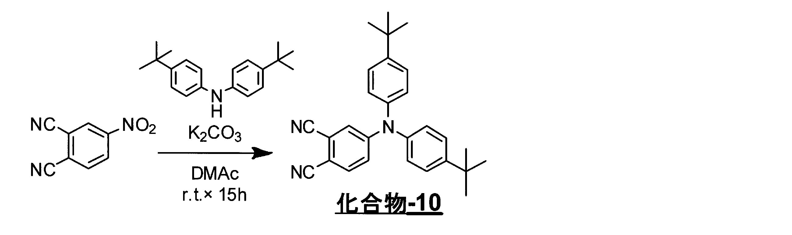
下記に示す合成ルートにより、比較化合物S-2を合成した。

冷却管の付いた三つ口フラスコに、ジメチルホムルアミド10mL、4-ヨード-フタロニトリル0.13g、4-(メトキシカルボニル)フェニルボロン酸0.18g、1,4-ジアザビシクロ[2,2,2]オクタン0.5mL、炭酸セシウム0.54g、及び酢酸パラジウム(II)0.03gを加え、窒素気流下110℃まで加熱し4時間攪拌した。室温まで冷却後、反応液へジエチルエーテルおよび水を加えて抽出を行った。ジエチルエーテル層に水を加えて再度抽出を行った後、ジエチルエーテル層を硫酸マグネシウムで予備乾燥し、濃縮した。濃縮残渣をアルミナカラムクロマトグラフィーで精製する事により、化合物-11 0.08gを得た。
(2)化合物-12の合成
前記化合物-2と同様の方法により化合物-12 0.3gを得た。
(3)比較化合物S-2の合成
前記例示化合物A-2bと同様の方法により比較化合物S-2 0.08gを得た。
ミリマスの測定により同定を行った。
Mass実測値(m/z);(M+H)+:1513.3155
Mass計算値(m/z);(M+H)+:1513.3159(C87H69N8O2S6Zn)
Angew.Chem.Int.Ed.,46,8358(2007)に従い、下記比較化合物S-1を合成した。

前記合成例1~7で合成した金属錯体色素について、最大吸収波長を測定した。その結果を表1に示す。測定は、分光光度計(U-4100(商品名)、日立ハイテク社製)によって行い、溶液はTHF:エタノール=1:1を用い、濃度が2μMになるように調整した。

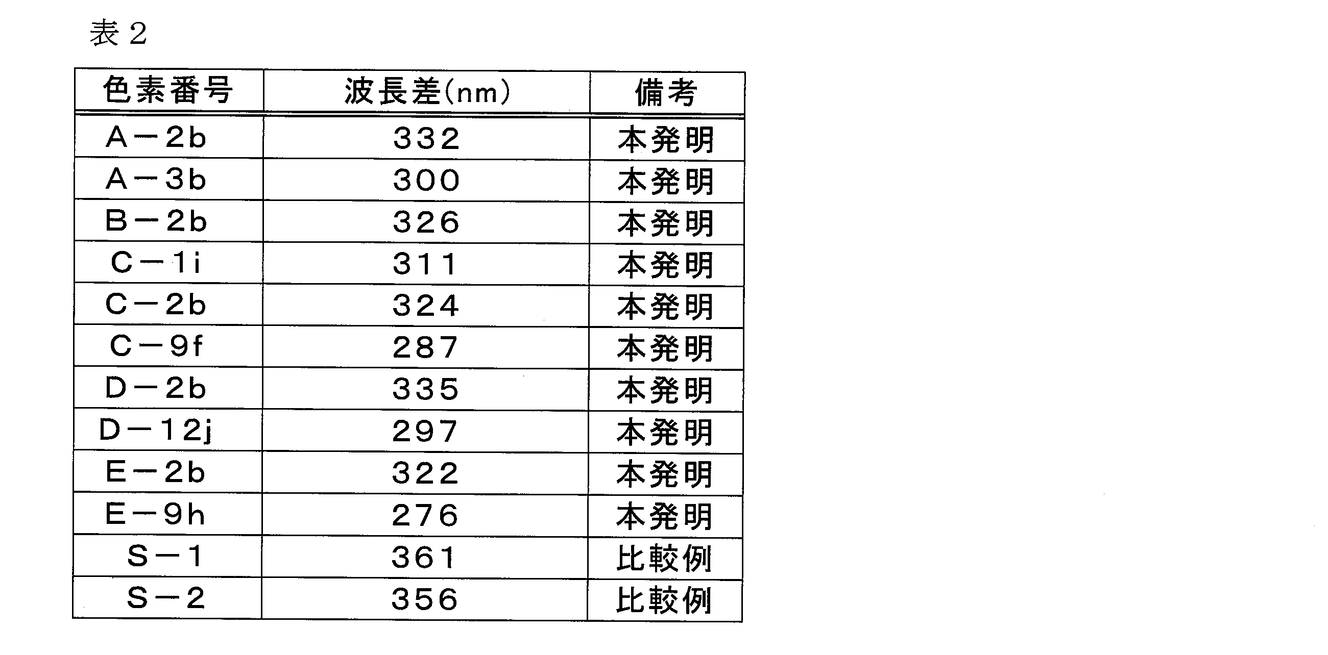
(光電変換素子の作製)
図1に示す光電変換素子10を以下のようにして作製した。
ガラス基板上に、透明導電膜としてフッ素をドープした酸化スズをスパッタリングにより形成し、これをレーザーでスクライブして、透明導電膜を2つの部分に分割した。
次に、水とアセトニトリルの容量比4:1からなる混合溶媒100mlにアナターゼ型酸化チタン(日本アエロジル社製のP-25(商品名))32gを配合し、自転/公転併用式のミキシングコンディショナーを使用して均一に分散、混合し、半導体微粒子分散液を得た。この分散液を透明導電膜に塗布し、500℃で加熱して受光電極を作製した。
その後、同様にシリカ粒子とルチル型酸化チタンとを40:60(質量比)で含有する分散液を作製し、この分散液を前記の受光電極に塗布し、500℃で加熱して絶縁性多孔体を形成した。次いで対極として炭素電極を形成した。
次に、下記表3に記載された増感色素のエタノール溶液(3×10⁻⁴mol/L)に、上記の絶縁性多孔体が形成されたガラス基板を48時間浸漬した。増感色素の染着したガラスを4-tert-ブチルピリジンの10%エタノール溶液に30分間浸漬した後、エタノールで洗浄し自然乾燥させた。このようにして得られる感光体層の厚さは10μmであり、半導体微粒子の塗布量は20g/m2であった。電解液は、ヨウ化ジメチルプロピルイミダゾリウム(0.5mol/L)、ヨウ素(0.1mol/L)のメトキシプロピオニトリル溶液を用いた。
500Wのキセノンランプ(ウシオ製)の光をAM1.5Gフィルター(商品名、Oriel社製)及びシャープカットフィルター(KenkoL-42、商品名)を通すことにより紫外線を含まない模擬太陽光を発生させた。この光の強度は89mW/cm2であった。作製した光電変換素子にこの光を照射し、発生した電気を電流電圧測定装置(ケースレー238型、商品名)にて測定した。また、作製した光電変換素子の400~800nmにおける光電変換効率をペクセル社製のIPCE測定装置にて測定した。これらにより求められた光電気化学電池の変換効率を測定した結果、および450nmにおける光電変換効率(IPCE)を下記表3に示した。変換効率の結果は、変換効率が3.5%以上のものを◎、2.5%以上3.5%未満のものを○、2.0%以上2.5%未満のものを△、2.0%未満のものを×として評価した。
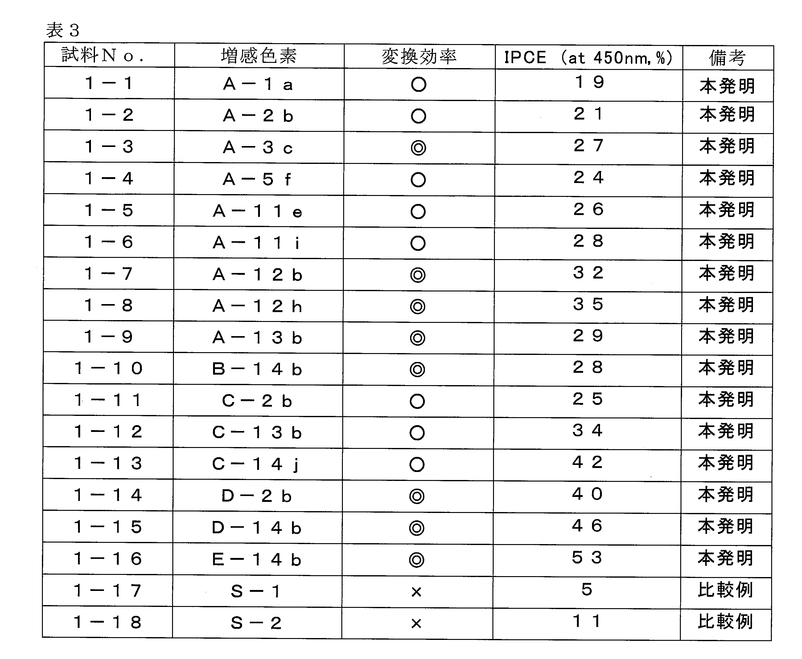
それに対して、試料番号1-17及び1-18の比較例は、変換効率は2.0%未満と不十分であった。
ガラス基板上にITO(インジウム・スズ・オキサイド)膜を作製し、その上にFTO(フッ素ドープ酸化スズ)膜を積層することにより、透明導電膜を作製した。その後透明導電膜上に酸化物半導体多孔質膜を形成することにより、透明電極板を得た。そしてその透明電極板を使用して光電気化学電池を作製し、変換効率を測定した。その方法は以下の(1)~(5)の通りである。
塩化インジウム(III)四水和物5.58gと塩化スズ(II)二水和物0.23gとをエタノール100mlに溶解して、ITO膜用原料化合物溶液とした。
塩化スズ(IV)五水和物0.701gをエタノール10mlに溶解し、これにフッ化アンモニウム0.592gの飽和水溶液を加え、この混合物を超音波洗浄機に約20分間かけ、完全に溶解して、FTO膜用原料化合物溶液とした。
厚さ2mmの耐熱ガラス板の表面を化学洗浄し、乾燥した後、このガラス板を反応器内に置き、ヒータで加熱した。ヒータの加熱温度が450℃になったところで、(1)で得られたITO膜用原料化合物溶液を、口径0.3mmのノズルから圧力0.06MPaで、ガラス板までの距離を400mmとして、25分間噴霧した。
このITO膜用原料化合物溶液の噴霧後、2分間(この間ガラス基板表面にエタノールを噴霧し続け、基板表面温度の上昇を抑えるようにした。)経過し、ヒータの加熱温度が530℃になった時に、(2)で得られたFTO膜用原料化合物溶液を同様の条件で2分30秒間噴霧した。これにより、耐熱ガラス板上に厚さ530nmのITO膜、厚さ170nmのFTO膜が順次形成された透明電極板が得られた。
比較のために、厚さ2mmの耐熱ガラス板上に同様に、厚さ530nmのITO膜のみを成膜した透明電極板と、同じく厚さ180nmのFTO膜のみを成膜した透明電極板とをそれぞれ作製した。
これら3種の透明電極板を加熱炉にて、450℃で2時間加熱した。
次に、上記3種の透明電極板を用いて、特許第4260494号明細書中の図2に示した構造の光電気化学電池を作製した。酸化物半導体多孔質膜15の形成は、平均粒径約230nmの酸化チタン微粒子をアセトニトリル100mlに分散してペーストとし、これを透明電極11上にバーコート法により厚さ15μmに塗布し、乾燥後450℃で1時間焼成して行い、この酸化物半導体多孔質膜15に表4記載の色素を担持した。色素溶液への浸漬条件は前記実験1と同じとした。
さらに、対極16には、ガラス板上にITO膜とFTO膜とを積層した導電性基板を使用し、電解質層17には、ヨウ素/ヨウ化物の非水溶液からなる電解液を用いた。光電気化学電池の平面寸法は25mm×25mmとした。
この光電気化学電池について、人工太陽光(AM1.5)を照射し、その変換効率を求めた。その結果を表4に示す。変換効率が3.5%以上のものを◎、2.5%以上3.5%未満のものを○、2.0%以上2.5%未満のものを△、2.0%未満のものを×として評価した。

FTO膜上に集電電極を配し、光電気化学電池を作製し、変換効率を評価した。評価は以下の通り、試験セル(i)と試験セル(iv)の2種類を用いた。
長さ100mm×幅100mm×厚さ2mmの耐熱ガラス板の表面を化学洗浄し、乾燥した後、このガラス板を反応器内に置き、ヒータで加熱した後、実験2で調製したFTO(フッ素ドープ酸化スズ)膜用原料化合物溶液を、口径0.3mmのノズルから圧力0.06MPaで、ガラス板までの距離を400mmとして、25分間噴霧し、FTO膜付きガラス基板を用意した。その表面に、エッチング法により深さ5μmの溝を格子回路パターン状に形成した。フォトリソグラフでパターン形成した後に、フッ酸を用いてエッチングを行った。これに、めっき形成を可能とするためにスパッタ法により金属導電層(シード層)を形成し、更にアディティブめっきにより金属配線層を形成した。金属配線層は、透明基板表面から凸レンズ状に3μm高さまで形成した。回路幅は60μmとした。この上から、遮蔽層としてFTO膜を400nmの厚さでSPD法により形成して、電極基板(i)とした。なお、電極基板(i)の断面形状は、特開2004-146425中の図2に示すものとなっていた。
電極基板(i)上に、平均粒径25nmの酸化チタンをアセトニトリル100mlに分散して得た分散液を塗布・乾燥し、450℃で1時間加熱・焼結した。これを表5に示す色素のエタノール溶液へ浸漬して色素を吸着させた。浸漬条件は実験1と同じとした。50μm厚の熱可塑性ポリオレフィン樹脂シートを介して白金スパッタFTO基板と対向して配置し、樹脂シート部を熱溶融させて両極板を固定した。
なおあらかじめ白金スパッタ極側に開けておいた電解液の注液口から、0.5Mのヨウ化塩と0.05Mのヨウ素とを主成分に含むメトキシアセトニトリル溶液を注液し、電極間に満たした。さらに周辺部及び電解液注液口をエポキシ系封止樹脂を用いて本封止し、集電端子部に銀ペーストを塗布して試験セル(i)とした。
試験セル(i)と同様の方法で長さ100×幅100mmのFTO膜付きガラス基板を用意した。そのFTOガラス基板上に、アディティブめっき法により金属配線層(金回路)を形成した。金属配線層(金回路)は基板表面に格子状に形成し、回路幅50μm、回路厚5μmとした。この表面に厚さ300nmのFTO膜を遮蔽層としてSPD法により形成して試験セル(iv)とした。電極基板(iv)の断面をSEM-EDXを用いて確認したところ、配線底部でめっきレジストの裾引きに起因すると思われる潜り込みがあり、影部分にはFTOが被覆されていなかった。
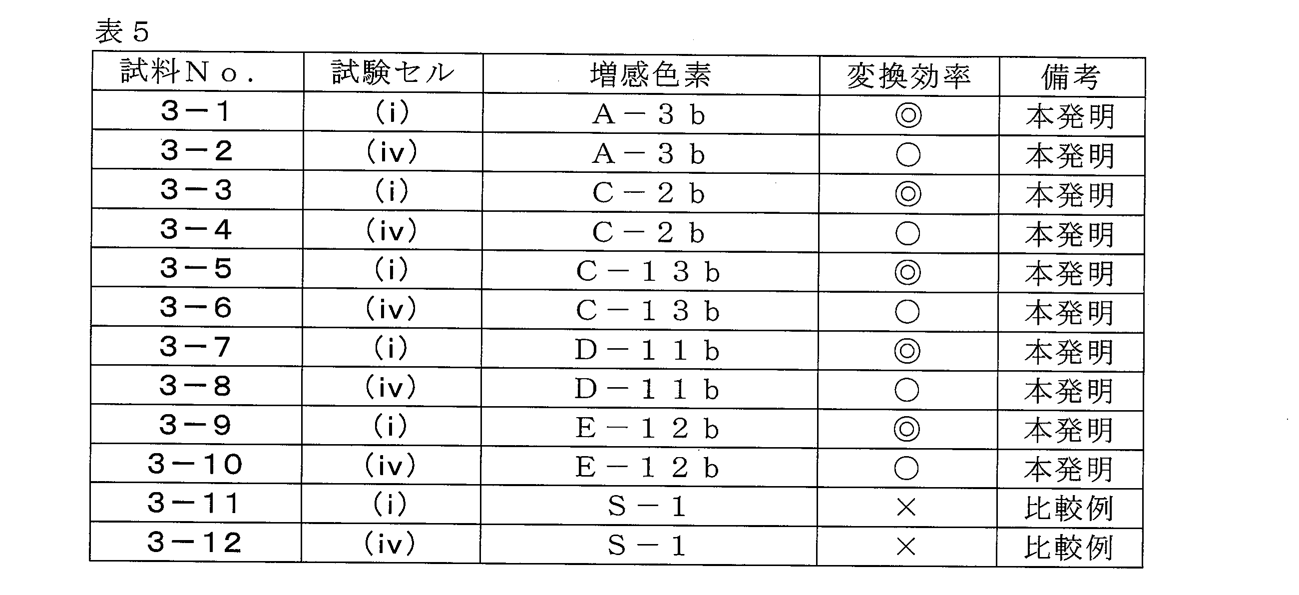
下記に示す通りに光電気化学電池(光電池セル)(A)~(D)を作製し、作成した光電池セルの変換効率を評価した。
(1)酸化物半導体膜形成用塗布液(A)の調製
5gの水素化チタンを1Lの純水に懸濁し、5質量%の過酸化水素液400gを30分かけて添加し、ついで80℃に加熱して溶解してペルオキソチタン酸の溶液を調製した。この溶液の全量から90容積%を分取し、濃アンモニア水を添加してpH9に調整し、オートクレーブに入れ、250℃で5時間、飽和蒸気圧下で水熱処理を行ってチタニアコロイド粒子(A)を調製した。得られたチタニアコロイド粒子(A)は、X線回折により結晶性の高いアナターゼ型酸化チタンであった。
次に、上記で得られたチタニアコロイド粒子(A)を10質量%まで濃縮し、前記ペルオキソチタン酸溶液を混合し、この混合液中のチタンをTiO2換算し、TiO2質量の30質量%となるように膜形成助剤としてヒドロキシプロピルセルロースを添加して半導体膜形成用塗布液(A)を調製した。
次いで、フッ素ドープした酸化スズが電極層として形成された透明ガラス基板上に前記塗布液(A)を塗布し、自然乾燥し、引き続き低圧水銀ランプを用いて6000mJ/cm2の紫外線を照射してペルオキソ酸を分解させ、塗膜を硬化させた。塗膜を300℃で30分間加熱してヒドロキシプロピルセルロースの分解及びアニーリングを行って酸化物半導体膜(A)をガラス基板に形成した。
次に、分光増感色素として表6に示す色素の濃度3×10⁻⁴mol/Lのエタノール溶液を調製した。この色素溶液を100rpmスピナーで、酸化物半導体膜(A)上へ塗布して乾燥した。この塗布及び乾燥工程を5回行った。
アセトニトリルと炭酸エチレンとの体積比が1:5の混合溶媒に、テトラプロピルアンモニウムアイオダイドを0.46mol/L、ヨウ素を0.07mol/Lの濃度となるように溶解して電解質溶液を調製した。
前記(3)で作製した、色素を吸着させた酸化物半導体膜(A)が形成されたガラス基板を一方の電極とし、他方の電極として、フッ素ドープした酸化スズを電極として形成しその上に白金を担持した透明ガラス基板を対向して配置し、側面を樹脂にてシールし、電極間に前記(4)で調製したの電解質溶液を封入し、さらに電極間をリード線で接続して光電気セル(A)を作製した。
光電気セル(A)は、ソーラーシュミレーターで100W/m2の強度の光を照射して、η(変換効率)を測定した。その結果を表6に示した。
紫外線を照射してペルオキソ酸を分解させ、塗膜を硬化させた後、Arガスのイオン照射(日新電気製:イオン注入装置、200eVで10時間照射)を行った以外は、酸化物半導体膜(A)と同様にして酸化物半導体膜(B)を形成した。
酸化物半導体膜(A)と同様に、酸化物半導体膜(B)に表6に示す色素の吸着を行った。
その後光電池セル(A)と同様の方法で光電気セル(B)を作成し、変換効率を測定した。その結果を表6に示した。
18.3gの4塩化チタンを純水で希釈して、TiO2換算で1.0質量%含有する水溶液を得た。この水溶液を撹拌しながら、15質量%のアンモニア水を添加し、pH9.5の白色スラリーを得た。このスラリーを濾過洗浄し、TiO2換算で、10.2質量%の水和酸化チタンゲルのケーキを得た。このケーキと5質量%過酸化水素液400gを混合し、ついで80℃に加熱して溶解してペルオキソチタン酸の溶液を調製した。この溶液全量から90体積%を分取し、これに濃アンモニア水を添加してpH9に調整し、オートクレーブに入れ、250℃で5時間、飽和蒸気圧下で水熱処理を行ってチタニアコロイド粒子(C)を調製した。
次に、上記で得られたペルオキソチタン酸溶液とチタニアコロイド粒子(C)を使用して酸化物半導体膜(A)と同様にして酸化物半導体膜(C)を形成した。さらに、金属酸化物半導体膜(A)と同様にして、分光増感色素として表6に示す色素の吸着を行った。
その後光電気セル(A)と同様の方法で光電気セル(C)を作製し、変換効率を測定した。その結果を表6に示した。
18.3gの4塩化チタンを純水で希釈してTiO2換算で1.0質量%含有する水溶液を得た。この水溶液を撹拌しながら、15質量%のアンモニア水を添加し、pH9.5の白色スラリーを得た。このスラリーを濾過洗浄した後、純水に懸濁してTiO2として0.6質量%の水和酸化チタンゲルのスラリーとし、これに塩酸を加えてpH2とした後、オートクレーブに入れ、180℃で5時間、飽和蒸気圧下で水熱処理を行ってチタニアコロイド粒子(D)を調製した。
次に、チタニアコロイド粒子(D)を10質量%まで濃縮し、これに、TiO2に換算して、30質量%となるように膜形成助剤としてヒドロキシプロピルセルロースを添加して、半導体膜形成用塗布液を調製した。次いで、フッ素ドープした酸化スズが電極層として形成された透明ガラス基板上に、前記塗布液を塗布し、自然乾燥し、引き続き低圧水銀ランプを用いて6000mJ/cm2の紫外線を照射し、膜を硬化させた。さらに、300℃で30分間加熱してヒドロキシプロピルセルロースの分解及びアニーリングを行い、酸化物半導体膜(D)を形成した。
次に、酸化物半導体膜(A)と同様にして表6に示す色素の吸着を行った。
その後、光電気セル(A)と同様の方法で光電気セル(D)を作成し、変換効率を測定した。結果を表6に示した。

下記に示すように、酸化チタンの調製又は合成を行い、得られた酸化チタンから酸化物半導体膜を作製し、光電気化学電池とし、その評価を行った。
市販のアナターゼ型酸化チタン(石原産業(株)製、商品名ST-01)を用い、これを約900℃に加熱してブルーカイト型の酸化チタン1に変換した。
(酸化チタン2(ブルーカイト型))
蒸留水954mLを還流冷却器付きの反応槽に装入し、95℃に加温する。撹拌速度を約200rpmに保ちながら、この蒸留水に四塩化チタン(Ti含有量:16.3質量%、比重1.59、純度99.9%)水溶液46mLを約5.0mL/minの速度で反応槽に滴下した。このとき、反応液の温度が下がらないように注意した。その結果、四塩化チタン濃度が0.25mol/L(酸化チタン換算2質量%)であった。反応槽中では反応液が滴下直後から、白濁し始めたがそのままの温度で保持を続け、滴下終了後さらに昇温し沸点付近(104℃)まで加熱し、この状態で60分間保持して完全に反応を終了した。
得られたゾルを濾過し、次いで60℃の真空乾燥器を用いて粉末とした。この粉末をX線回折法により定量分析した結果、(ブルーカイト型121面のピーク強度)/(三本が重なる位置でのピーク強度)比は0.38、(ルチル型のメインピーク強度)/(三本が重なる位置でのピーク強度)比は0.05であった。これらから求めると、得られた酸化チタンは、ブルーカイト型が約70.0質量%、ルチル型が約1.2質量%、アナターゼ型が約28.8質量%の結晶性であった。また、透過型電子顕微鏡でこの微粒子を観察したところ、1次粒子の平均粒径は0.015μmであった。
三塩化チタン水溶液(Ti含有量:28質量%、比重1.5、純度99.9%)を蒸留水で希釈し、チタン濃度換算で0.25mol/Lの溶液とした。このとき、液温が上昇しないよう氷冷して、50℃以下に保った。次に、この溶液を還流冷却器付きの反応槽に500mL投入し、85℃に加温しながらオゾンガス発生装置から純度80%のオゾンガスを1L/minでバブリングし、酸化反応を行なった。この状態で2時間保持し、完全に反応を終了した。
得られたゾルをろ過、真空乾燥し、粉末とした。この粉末をX線回折法により定量分析した結果、(ブルーカイト型121面のピーク強度)/(三本が重なる位置でのピーク強度)比は0.85、(ルチル型のメインピーク強度)/(三本が重なる位置でのピーク強度)比は0であった。これらから求めると、得られた酸化チタンは、ブルーカイト型が約98質量%、ルチル型が0質量%、アナターゼ型が0質量%であり、約2%は無定形であった。また、透過型電子顕微鏡でこの微粒子を観察したところ、1次粒子の平均粒径は0.05μmであった。
上記の酸化チタン1~3を半導体として、特開2000-340269の図1に示す構成を有する光電変換素子を次のように作製した。
ガラス基板上にフッ素ドープの酸化スズをコートし、導電性透明電極とした。電極面上にそれぞれの酸化チタン粒子を原料としたペーストを作成し、バーコート法で厚さ50μmに塗布した後、500℃で焼成して膜厚約20μmの薄層を形成した。次に表7に示す色素の3×10⁻⁴モル濃度のエタノール溶液を調製し、これに上記の酸化チタンの薄層を形成したガラス基板を浸漬し、12時間室温で保持した。
なお、変換効率が3.5%以上のものを◎、2.5%以上3.5%未満のものを○、2.0%以上2.5%未満のものを△、2.0%未満のものを×として表示した。

下記に示すように、粒径の異なる酸化チタンを含有する半導体電極を用いて光電気化学電池を作製し、その特性を評価した。
[ペーストの調製]
まず光電気化学電池を構成する半導体電極の半導体層又は光散乱層を形成するためのペーストを以下の手順で調製した。
球形のTiO2粒子(アナターゼ型、平均粒径;25nm、以下、球形TiO2粒子1という)を硝酸溶液に入れて撹拌することによりチタニアスラリーを調製した。次に、チタニアスラリーに増粘剤としてセルロース系バインダーを加え、混練してペースト1を調製した。
球形TiO2粒子1と、別の球形のTiO2粒子(アナターゼ型、平均粒径;200nm、以下、球形TiO2粒子2という)とを硝酸溶液に入れて撹拌することによりチタニアスラリーを調製した。次に、チタニアスラリーに増粘剤としてセルロース系バインダーを加え、混練してペースト2(TiO2粒子1の質量:TiO2粒子2の質量=30:70)を調製した。
前記ペースト1と、棒状のTiO2粒子(アナターゼ型、直径;100nm、アスペクト比;5、以下、棒状TiO2粒子1という)とを混合し、棒状TiO2粒子1の質量:ペースト1の質量=10:90のペースト3を調製した。
前記ペースト1と、棒状TiO2粒子1とを混合し、棒状TiO2粒子1の質量:ペースト1の質量=30:70のペースト4を調製した。
前記ペースト1と、棒状TiO2粒子1とを混合し、棒状TiO2粒子1の質量:ペースト1の質量=50:50のペースト5を調製した。
前記ペースト1と、板状のマイカ粒子(直径;100nm、アスペクト比;6、以下、板状マイカ粒子1という)とを混合し、板状マイカ粒子1の質量:ペースト1の質量=20:80のペースト6を調製した。
前記ペースト1と、棒状のTiO2粒子(アナターゼ、直径;30nm、アスペクト比;6.3、以下、棒状TiO2粒子2という)とを混合し、棒状TiO2粒子2の質量:ペースト1の質量=30:70のペースト7を調製した。
前記ペースト1と、棒状のTiO2粒子(アナターゼ、直径;50nm、アスペクト比;6.1、以下、棒状TiO2粒子3という)とを混合し、棒状TiO2粒子3の質量:ペースト1の質量=30:70のペースト8を調製した。
前記ペースト1と、棒状のTiO2粒子(アナターゼ、直径;75nm、アスペクト比;5.8、以下、棒状TiO2粒子4という)とを混合し、棒状TiO2粒子4の質量:ペースト1の質量=30:70のペースト9を調製した。
前記ペースト1と、棒状のTiO2粒子(アナターゼ、直径;130nm、アスペクト比;5.2、以下、棒状TiO2粒子5という)とを混合し、棒状TiO2粒子5の質量:ペースト1の質量=30:70のペースト10を調製した。
前記ペースト1と、棒状のTiO2粒子(アナターゼ、直径;180nm、アスペクト比;5、以下、棒状TiO2粒子6という)とを混合し、棒状TiO2粒子6の質量:ペースト1の質量=30:70のペースト11を調製した。
前記ペースト1と、棒状のTiO2粒子(アナターゼ、直径;240nm、アスペクト比;5、以下、棒状TiO2粒子7という)とを混合し、棒状TiO2粒子7の質量:ペースト1の質量=30:70のペースト12を調製した。
前記ペースト1と、棒状のTiO2粒子(アナターゼ、直径;110nm、アスペクト比;4.1、以下、棒状TiO2粒子8という)とを混合し、棒状TiO2粒子8の質量:ペースト1の質量=30:70のペースト13を調製した。
前記ペースト1と、棒状のTiO2粒子(アナターゼ、直径;105nm、アスペクト比;3.4、以下、棒状TiO2粒子9という)とを混合し、棒状TiO2粒子9の質量:ペースト1の質量=30:70のペースト14を調製した。
(光電気化学電池1)
以下に示す手順により、特開2002-289274記載の図5に示した光電極12と同様の構成を有する光電極を作製し、更に、光電極を用いて、当該光電極以外は色素増感型太陽電池20と同様の構成を有する10×10mmのスケールの光電気化学電池1を作製した。
まずマグネシウムエトキシドで脱水した無水エタノールを溶媒として、これに表8に示す色素を、その濃度が3×10⁻⁴mol/Lとなるように溶解し、色素溶液を調製した。次に、この溶液に半導体電極を浸漬し、これにより、半導体電極に色素を約1.5ミリモル/m2吸着し、光電極を完成させた。
半導体電極の製造を以下のようにして行ったこと以外は、光電気化学電池1と同様の手順により特開2002-289274記載の図1に示した光電極10及び特開2002-289274記載の図3に示した色素増感型太陽電池20と同様の構成を有する光電極及び光電気化学電池2を作製した。
半導体電極の製造に際して、前記ペースト1を半導体層形成用ペーストとして使用し、前記ペースト4を光散乱層形成用ペーストとして使用したこと以外は、光電気化学電池1と同様の手順により特開2002-289274記載の図5に示した光電極10及び特開2002-289274記載の図3に示した光電気化学電池20と同様の構成を有する光電極及び光電気化学電池3を作製した。なお、半導体電極は、受光面の面積;10mm×10mm、層厚;10μm、半導体層の層厚;5μm、光散乱層の層厚;5μm、光散乱層に含有される棒状TiO2粒子1の含有率;30質量%であった。
半導体電極の製造に際して、前記ペースト2を半導体層形成用ペーストとして使用し、前記ペースト6を光散乱層形成用ペーストとして使用したこと以外は、光電気化学電池1と同様の手順により特開2002-289274記載の図5に示した光電極10及び特開2002-289274記載の図3に示した光電気化学電池20と同様の構成を有する光電極及び光電気化学電池4を作製した。なお、半導体電極は、受光面の面積;10mm×10mm、層厚;10μm、半導体層の層厚;6.5μm、光散乱層の層厚;3.5μm、光散乱層に含有される板状マイカ粒子1の含有率;20質量%であった。
半導体電極の製造に際して、前記ペースト2を半導体層形成用ペーストとして使用し、前記ペースト8を光散乱層形成用ペーストとして使用したこと以外は、光電気化学電池1と同様の手順により特開2002-289274記載の図5に示した光電極10及び特開2002-289274記載の図3に示した光電気化学電池20と同様の構成を有する光電極及び光電気化学電池5を作製した。なお、半導体電極の光散乱層に含有される棒状TiO2粒子3の含有率;30質量%であった。
半導体電極の製造に際して、前記ペースト2を半導体層形成用ペーストとして使用し、前記ペースト9を光散乱層形成用ペーストとして使用したこと以外は、光電気化学電池1と同様の手順により特開2002-289274記載の図5に示した光電極10及び特開2002-289274記載の図3に示した光電気化学電池20と同様の構成を有する光電極及び光電気化学電池6を作製した。なお、半導体電極の光散乱層に含有される棒状TiO2粒子4の含有率;30質量%であった。
半導体電極の製造に際して、前記ペースト2を半導体層形成用ペーストとして使用し、前記ペースト10を光散乱層形成用ペーストとして使用したこと以外は、光電気化学電池1と同様の手順により特開2002-289274記載の図5に示した光電極10及び特開2002-289274記載の図3に示した光電気化学電池20と同様の構成を有する光電極及び光電気化学電池7を作製した。なお、半導体電極の光散乱層に含有される棒状TiO2粒子5の含有率;30質量%であった。
半導体電極の製造に際して、前記ペースト2を半導体層形成用ペーストとして使用し、前記ペースト11を光散乱層形成用ペーストとして使用したこと以外は、光電気化学電池1と同様の手順により特開2002-289274記載の図5に示した光電極10及び特開2002-289274記載の図3に示した光電気化学電池20と同様の構成を有する光電極及び光電気化学電池8を作製した。なお、半導体電極の光散乱層に含有される棒状TiO2粒子6の含有率;30質量%であった。
半導体電極の製造に際して、前記ペースト2を半導体層形成用ペーストとして使用し、前記ペースト13を光散乱層形成用ペーストとして使用したこと以外は、光電気化学電池1と同様の手順により特開2002-289274記載の図5に示した光電極10及び特開2002-289274記載の図3に示した光電気化学電池20と同様の構成を有する光電極及び光電気化学電池9を作製した。なお、半導体電極の光散乱層に含有される棒状TiO2粒子8の含有率;30質量%であった。
半導体電極の製造に際して、前記ペースト2を半導体層形成用ペーストとして使用し、前記ペースト14を光散乱層形成用ペーストとして使用したこと以外は、光電気化学電池1と同様の手順により特開2002-289274記載の図5に示した光電極10及び特開2002-289274記載の図3に示した光電気化学電池20と同様の構成を有する光電極及び光電気化学電池10を作製した。なお、半導体電極の光散乱層に含有される棒状TiO2粒子9の含有率;30質量%であった。
半導体電極の製造に際して、前記ペースト2のみを用いて半導体層のみからなる半導体電極(受光面の面積;10mm×10mm、層厚;10μm、)を作製したこと以外は、光電気化学電池1と同様の手順により光電極及び光電気化学電池11を作製した。
半導体電極の製造に際して、前記ペースト2を半導体層形成用ペーストとして使用し、前記ペースト7を光散乱層形成用ペーストとして使用したこと以外は、光電気化学電池1と同様の手順により特開2002-289274記載の図5に示した光電極10及び特開2002-289274記載の図3に示した光電気化学電池20と同様の構成を有する光電極及び光電気化学電池12を作製した。なお、半導体電極の光散乱層に含有される棒状TiO2粒子2の含有率;30質量%であった。
電池特性試験を行ない、光電気化学電池1~12について変換効率ηを測定した。電池特性試験は、ソーラーシミュレータ(WACOM製、商品名WXS-85H)を用い、AM1.5フィルターを通したキセノンランプから1000W/m2の疑似太陽光を照射することにより行った。I-Vテスターを用いて電流-電圧特性を測定し、エネルギー変換効率(η/%)を求めた。その結果を表8に示す。
なお、変換効率が3.5%以上のものを◎、2.5%以上3.5%未満のものを○、2.0%以上2.5%未満のものを△、2.0%未満のものを×として評価した。

金属酸化物微粒子に金属アルコキシドを加えスラリー状としたものを導電性基板に塗布し、その後、UVオゾン照射、UV照射又は乾燥を行い、電極を作製した。その後、光電気化学電池を作製し、変換効率を測定した。
金属酸化物微粒子としては、酸化チタンを用いた。酸化チタンは、質量比で、30%ルチル型及び70%アナターゼ型、平均粒径25nmのP25粉末(Degussa社製、商品名)を用いた。
金属酸化物微粒子をあらかじめ熱処理することで表面の有機物と水分を除去した。酸化チタン微粒子の場合は450℃のオーブンで大気下、30分間加熱した。
温度26℃、湿度72%の環境に保存しておいた酸化チタン、P25粉末(Degussa社製、商品名)に含まれる水分量を、熱重量測定における重量減少、及び300℃に加熱したときに脱着した水分量のカールフィッシャー滴定により定量した。
金属酸化物微粒子を結合する役割をする金属アルコキシドとしては、チタン原料としてはチタン(IV)テトライソプロポキシド(TTIP)、ジルコニウム原料としてはジルコニウム(IV)テトラn-プロポキシド、ニオブ原料としてはニオブ(V)ペンタエトキシド(全てAldrich社製)をそれぞれ用いた。
同様に、酸化チタン微粒子とTTIP以外のアルコキシドの混合ペーストについても微粒子濃度が22質量%となるように調製した。酸化亜鉛及び酸化スズ微粒子を用いたペーストでは16質量%とした。酸化亜鉛及び酸化スズの場合は、金属酸化物微粒子1gに対して、金属アルコキシド溶液5.25gの比で混合した。
導電性基板へのペーストの塗布方法は、ドクターブレード法、スクリーン印刷法、スプレー塗布法などを用いることが可能であり、適当なペースト粘度は塗布方法によって適宜選択した。ここでは簡便にガラス棒で塗布する方法(ドクターブレード法に類似)を用いた。この場合、適当なペースト粘度を与える金属酸化物微粒子の濃度は概ね5~30質量%の範囲となった。
スズドープ酸化インジウム(ITO)導電膜付きポリエチレンテレフタレート(PET)フィルム基板(20Ω/cm2)又はフッ素ドープ酸化スズ(FTO)導電膜付きガラス基板(10Ω/cm2)に、スペーサーとして粘着テープ2枚を一定間隔で平行に貼り付け、上記の方法に従って調製した各ペーストを、ガラス棒を用いて均一に塗布した。
(乾燥処理)
導電性基板へ塗布した後の膜を大気中室温で2分程度で風乾した。この過程でペースト中の金属アルコキシドが大気中の水分によって加水分解を受け、Tiアルコキシド、Zrアルコキシド、Nbアルコキシドからそれぞれアモルファスの酸化チタン、酸化ジルコニウム、酸化ニオブが形成された。
生成したアモルファス金属酸化物が、金属酸化物微粒子同士及び膜と導電性基板を接着する役割を果たすため、風乾するのみで機械的強度と付着性に優れた多孔質膜が得られた。
UVオゾン処理には日本レーザー電子社製のNL-UV253 UVオゾンクリーナーを用いた。UV光源には185nmと254nmに輝線を持つ4.5W水銀ランプ3個を備えており、試料を光源から約6.5センチの距離に水平に配置した。チャンバー中に酸素気流を導入することでオゾンが発生する。本実施例においてはこのUVオゾン処理を2時間行なった。なお、このUVオゾン処理によるITO膜及びFTO膜の導電性の低下は全く見られなかった。
チャンバー中を窒素置換して処理を行う以外は同様に、前記UVオゾン処理と同様に、2時間処理を行った。このUV処理によるITO膜及びFTO膜の導電性の低下はまったく見られなかった。
増感色素として表9に示す色素を用い、0.5mMのエタノール溶液を調製した。本実施例では上記のプロセスで作製した多孔質膜を100℃のオーブンで1時間乾燥した後に増感色素の溶液に浸漬し、そのまま室温で50分間放置して酸化チタン表面に増感色素を吸着した。増感色素吸着後の試料はエタノールで洗浄し、風乾した。
色素吸着後の多孔質膜が形成された導電性基板を光電極とし、これと白金微粒子をスパッタリングにより修飾したITO/PETフィルム又はFTO/ガラス対極を対向させて、光電気化学電池を試作した。上記光電極の実効面積は約0.2cm2とした。電解質溶液には0.5MのLiI,0.05MのI2,0.5Mのt-ブチルピリジンを含む3-メトキシプロピオニトリルを用い、毛管現象によって両電極間のギャップに導入した。
なお、変換効率が2.5%以上のものを◎、2.0%以上2.5%未満のものを○、1.5%以上2.0%未満のものを△、1.5%未満のものを×として評価した。

表9において、「UVオゾン」、「UV」、「乾燥」の欄はそれぞれ、多孔質膜の形成後、増感色素吸着前における、UVオゾン処理、UV照射処理、乾燥処理の有無を表す。処理したものが「○」で示し、処理なしのものを「×」で示す。
溶媒としてアセトニトリルを用い、ヨウ化リチウム0.1mol/l、ヨウ素0.05mol/L、ヨウ化ジメチルプロピルイミダゾリウム0.62mol/lを溶解した電解質溶液を調製した。ここに下記に示すNo.1~No.8のベンズイミダゾール系化合物をそれぞれ濃度0.5mol/Lになるように別々に添加し、溶解した。

ここにポリエチレンフィルム製のフレーム型スペーサー(厚さ25μm)をのせ、白金対電極でこれを覆い、光電変換素子を作製した。
開放電圧は、6.3V以上のものを◎、6.0V以上6.3V未満のものを○、5.7V以上6.0V未満のものを△、5.7V未満のものを×として評価した。
変換効率は、3.5%以上のものを◎、2.5%以上3.5%未満のものを○、2.0%以上2.5%未満のものを△、2.0%未満のものを×として評価した。
なお、表10には、ベンズイミダゾール系化合物を加えていない電解液を用いた光電変換素子の結果も示した。
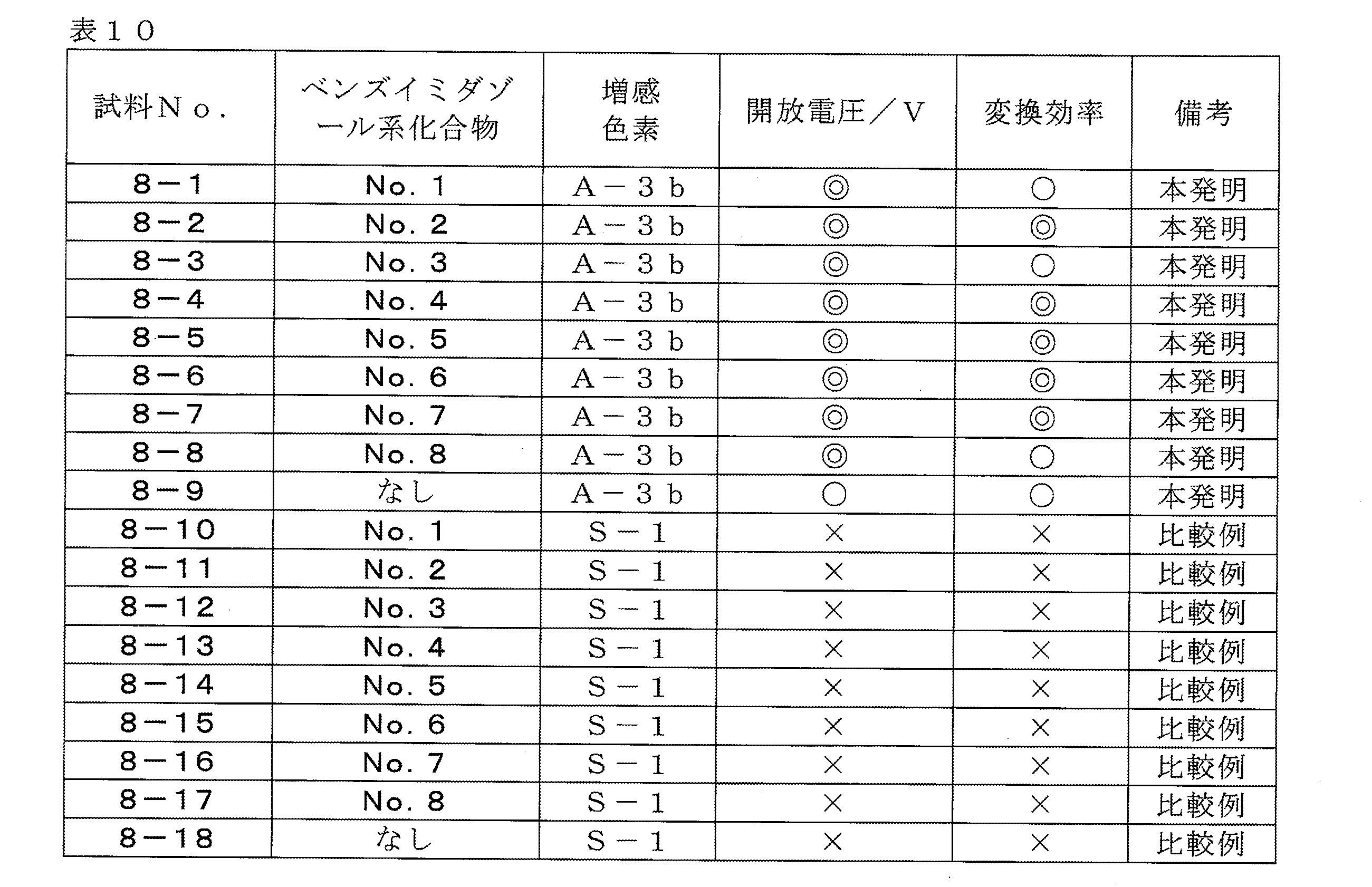
(光電気化学電池21)
以下に示す手順により、特開2004-152613記載の図1に示した光電極10と同様の構成を有する光電極(ただし、半導体電極2を2層構造とした。)を作製し、更に、この光電極を用いた以外は特開2004-152613記載の図1に示した色素増感型太陽電池20と同様の構成を有する光電気化学電池21(半導体電極2の受光面F2の面積:1cm2)を作製した。なお、2層構造を有する半導体電極2の各層について、透明電極1に近い側に配置される層を「第1の層」、対極CEに近い側に配置される層を「第2の層」という。
液状電解質におけるヨウ化亜鉛の濃度を50mmol/Lとしたこと以外は、光電気化学電池21と同様の手順及び条件で光電気化学電池22を作製した。
液状電解質におけるヨウ化亜鉛の代わりにヨウ化リチウムを添加し、液状電解質におけるヨウ化リチウムの濃度を20mmol/Lとしたこと以外は、光電気化学電池21と同様の手順及び条件で光電気化学電池23を作製した。
液状電解質におけるヨウ化亜鉛の代わりにヨウ化リチウムを添加し、液状電解質におけるヨウ化リチウムの濃度を100mmol/Lとしたこと以外は、光電気化学電池21と同様の手順及び条件で光電気化学電池24を作製した。
以下の手順により、光電気化学電池21~24について、光電変換効率(η(%))を測定した。
なお、Freshの変換効率は、3.5%以上のものを◎、2.5%以上3.5%未満のものを○、2.0%以上2.5%未満のものを△、2.0%未満のものを×として評価した。

1.二酸化チタン分散液の調製
内側をフッ素樹脂コーティングした内容積200mlのステンレス製容器に二酸化チタン微粒子(日本アエロジル(株)製、商品名:Degussa P-25)15g、水45g、分散剤(アルドリッチ社製、商品名:Triron X-100)1g、直径0.5mmのジルコニアビーズ(ニッカトー社製)30gを入れ、サンドグラインダーミル(アイメックス社製)を用いて1500rpmで2時間分散処理した。得られた分散液からジルコニアビーズを濾別した。得られた分散液中の二酸化チタン微粒子の平均粒径は2.5μmであった。なお粒径はMALVERN社製のマスターサイザー(商品名)により測定した。
フッ素をドープした酸化スズを被覆した20mm×20mmの導電性ガラス板(旭ガラス(株)製、商品名:TCOガラス-U、表面抵抗:約30Ω/m2)を準備し、その導電層側の両端(端から3mmの幅の部分)にスペーサー用粘着テープを張った後で、導電層上にガラス棒を用いて上記分散液を塗布した。分散液の塗布後、粘着テープを剥離し、室温で1日間風乾した。次にこの半導体塗布ガラス板を電気炉(ヤマト科学(株)製マッフル炉FP-32型)に入れ、450℃で30分間焼成した。半導体塗布ガラス板を取り出し冷却した後、表12に示す増感色素のエタノール溶液(濃度:3×10-4mol/L)に3時間浸漬した。増感色素が吸着した半導体塗布ガラス板を4-tert-ブチルピリジンに15分間浸漬した後、エタノールで洗浄し、自然乾燥させて、増感色素を吸着した酸化チタン微粒子層(電極A)を得た。電極Aの色素増感酸化チタン微粒子層の厚さは10μmであり、酸化チタン微粒子の塗布量は20g/m2であった。また色素の吸着量は、その種類に応じて0.1~10mmol/m2の範囲内であった。
色素増感太陽電池a~cの3タイプの色素増感太陽電池を以下の方法で作製した。これらの色素増感太陽電池において、表12に示す増感色素、下記窒素含有高分子α及び下記求電子剤βを用いて、試料番号10-1~10-15を得た。
(a)色素増感太陽電池aの作製
溶媒としては、アセトニトリルと3-メチル-2-オキサゾリジノンとの体積比90/10の混合物を用いた。この溶媒に、ヨウ素と電解質塩として、1-メチル-3-ヘキシルイミダゾリウムのヨウ素塩を加えて、0.5mol/Lの電解質塩および0.05mol/Lのヨウ素を含んだ溶液を調製した。この溶液に、(溶媒+窒素含有高分子化合物+塩)100質量部に対し、下記窒素含有高分子化合物αを10質量部加えた。さらに下記窒素含有高分子化合物αの反応性窒素原子に対する下記求電子剤βを0.1モル混合し、均一な反応溶液とした。
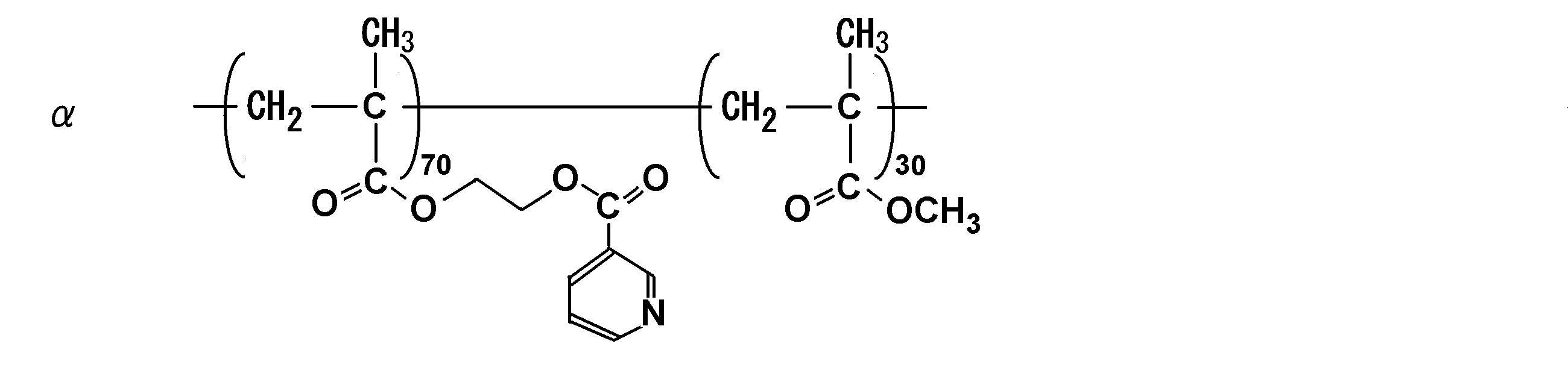

次いで80℃で30分間加熱して、架橋反応を行った。このようにして、特開2000-323190号公報の図2に示す通り、導電性ガラス板10の導電層12上に、色素増感酸化チタン微粒子層20、電解質層30、および白金薄膜42およびガラス板41からなる対極40が順に積層された本発明の色素増感太陽電池a-1(試料番号10-1)を得た。
また色素を表12に示すように変更した以外上記工程を繰り返すことにより、色素増感太陽電池a-2~a-5を得た。
前述のようにして増感色素を吸着させた酸化チタン微粒子層からなる電極A(20mm×20mm)を同じ大きさの白金蒸着ガラス板にスペーサーを介して重ねあわせた。次に両ガラス板の隙間に毛細管現象を利用して電解液(アセトニトリルと3-メチル-2-オキサゾリジノンとの体積比90/10の混合物を溶媒としたヨウ素0.05mol/L、ヨウ化リチウム0.5mol/Lの溶液)を浸透させて、色素増感太陽電池b-1(試料番号10-2)を作製した。また、色素を表12に示すように変更した以外上記工程を繰り返すことにより、色素増感太陽電池b-2~b-5を得た。
前述のようにして増感色素を吸着させた酸化チタン微粒子層からなる電極A(20mm×20mm)上に、電解液を塗布し、含浸させた。なお電解液は、ヘキサエチレングリコールメタクリル酸エステル(日本油脂化学(株)製,ブレンマーPE-350)1gと、エチレングリコール1gと、重合開始剤として2-ヒドロキシ-2-メチル-1-フェニル-プロパン-1-オン(日本チバガイギー(株)製,ダロキュア1173)20mgを含有した混合液に、ヨウ化リチウム500mgを溶解し10分間真空脱気することにより得た。次に前記混合溶液を含浸させた多孔性酸化チタン層を減圧下に置くことにより、多孔性酸化チタン層中の気泡を除き、モノマーの浸透を促した後、紫外光照射により重合して高分子化合物の均一なゲルを多孔性酸化チタン層の微細空孔内に充填した。このようにして得られたものをヨウ素雰囲気に30分間曝して、高分子化合物中にヨウ素を拡散させた後、白金蒸着ガラス板を重ね合わせ、色素増感太陽電池c-1(試料番号10-3)を得た。また色素を表12に示すように変更した以外上記工程を繰り返すことにより、光電気化学電池c-2~c-5を得た。
500Wのキセノンランプ(ウシオ電機(株)製)の光をAM1.5フィルター(Oriel社製)およびシャープカットフィルター(商品名:Kenko L-42)を通すことにより、紫外線を含まない模擬太陽光とした。光強度は89mW/cm2とした。
なお、Freshの変換効率は、3.5%以上のものを◎、2.5%以上3.5%未満のものを○、2.0%以上2.5%未満のものを△、2.0%未満のものを×として評価した。
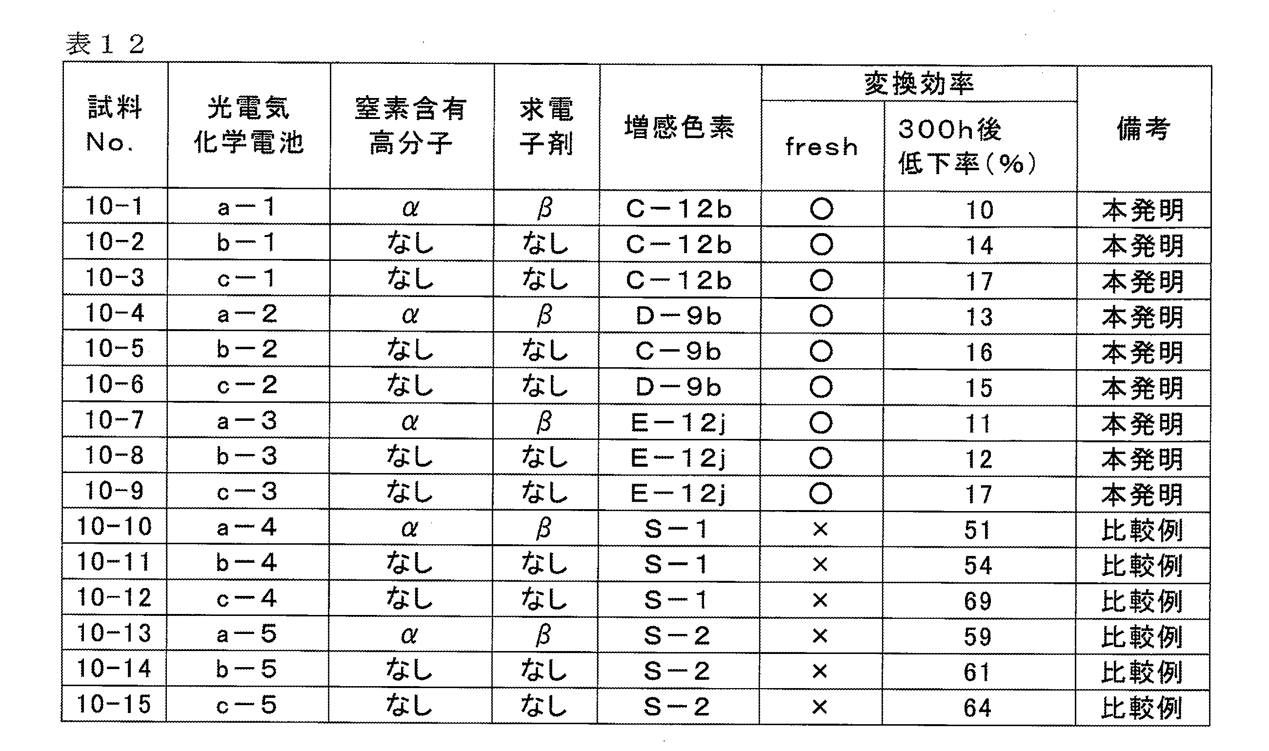
ゾル-ゲル法によって調製した懸濁液を用いてスクリーン印刷によりTiO2の多孔質層をFTOガラス上に塗布し450℃で焼成した。これに本発明の金属錯体色素A-2b、又は比較色素S-1の10-4mol/Lエタノール溶液中に浸漬することで、色素を吸着させた。
100mgの2,2′,7,7′ーテトラキス(ジフェニルアミノ)-9,9′ースピロビフルオレンを5mlのクロロホルムに溶解した。溶液を染料表面にそれを軽く塗ることによって、この溶液を層の細孔内にしみこませた。次に溶液の一滴を直接表面に置いて室温で乾燥した。ついで被覆支持体を蒸着装置に装着して約10-5ミリバールの真空下の熱蒸着によってさらに厚さ100nmの2,2′,7,7′ーテトラキス(ジフェニルアミノ)-9,9′ースピロビフルオレンの層を適用した。さらに蒸着装置内でこの被覆支持体に対極として厚さ200nmの金の層を被覆した。
このように調製した試料を高圧ランプ、光学フィルター、レンズ及びマウンティングを含む光学装置に取り付けた。フィルターの使用及びレンズの移動によって強度を変えることができた。金の層とSnO2層とに接点を付け、試料を照射している間電流測定装置に示した装置に取り付けた。測定のために、適当な光学フィルターを用い波長が430nm未満の光を遮断した。さらに放射線の強度を約1000W/m2にほぼ一致するように装置を調整した。
金の層及びSnO2層に接点を付け、また試料を照射している間は両接点をポテンシオスタットに接続した。外部電圧をかけずにS-1を用いた試料では約90nAの電流を生じたが、本発明の金属錯体色素A-2bを用いた試料では約190nAの電流を生じた。
この結果より、本発明の金属錯体色素を用いた光電気化学電池は、変換効率に優れることがわかる。
なお、どちらの試料の場合も照射しないと電流は消失した。
特開2000-90989の実施例1と同様に作成したタンデムセルにおいても、比較色素S-1を用いた光電気化学電池に比べ、本発明の金属錯体色素A-2bを用いた光電気化学電池では変換効率が高いことが確認できた。
チタンイソプロポキシド125mlを0.1M-硝酸水溶液(キシダ化学株式会社製)750mlに滴下し、80℃で8時間加熱して、加水分解反応をさせることにより、ゾル液を調製した。得られたゾル液をチタン製オートクレーブにて250℃で15時間保持し、粒子成長させ、その後、超音波分散を30分間行うことにより、平均一次粒径20nmの酸化チタン粒子を含むコロイド溶液を得た。
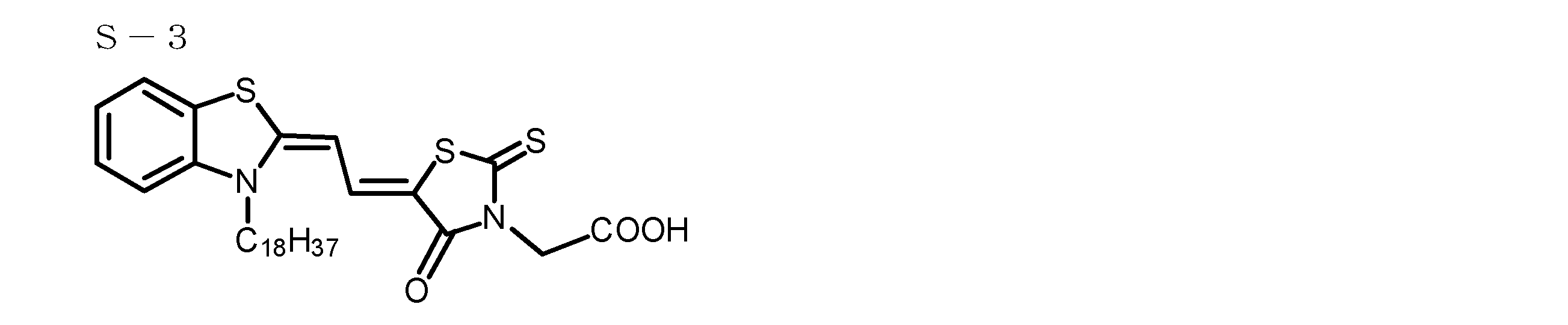
なお、変換効率は、3.5%以上のものを◎、2.5%以上3.5%未満のものを○、2.0%以上2.5%未満のものを△、2.0%未満のものを×として評価した。

市販の酸化チタン粒子(テイカ社製、平均粒径20nm)4.0gとジエチレングリコールモノメチルエーテル20mlとを、硬質ガラスビーズを使用してペイントシェイカーにより6時間分散させて酸化チタン懸濁液を作成した。次いで、この酸化チタン懸濁液を、ドクターブレードを用いて、予め酸化スズ導電層を付着させたガラス板(電極層)に塗布し、100℃で30分予備乾燥した後、電気炉で500℃で40分間焼成し、ガラス板上に酸化チタン膜(半導体材料)を形成した。
これとは別に、表14に示す増感色素をエタノールに溶解して光増感色素溶液を得た。この光増感色素溶液の濃度は5×10⁻⁴mol/Lであった。
次に、この溶液中に、膜状の酸化チタンが形成された前記のガラス板を入れ、60℃で60分間色素吸着を行った後、乾燥することにより、ガラス板上に半導体材料及び増感色素からなる光電変換層を形成した。さらに、光電変換層上に、ホール輸送材料としてのポリビニルカルバゾール(重量平均分子量3,000)のトルエン溶液(1%)を塗布して、減圧乾燥してホール輸送層を形成した。さらに、分子間電荷移動錯体としてのエチルカルバゾール1.95g及び5-ニトロナフトキノン2.03gを100mLアセトンに溶解して、得られた溶液をホール輸送層上に繰り返し塗布して伝導層を形成した。次いで、伝導層上に金電極(対極)を蒸着して光電変換素子を得た。
なお、変換効率は、1.5%以上のものを◎、1.0%以上1.5%未満のものを○、0.5%以上1.0%未満のものを△、0.5%未満のものを×として評価した。
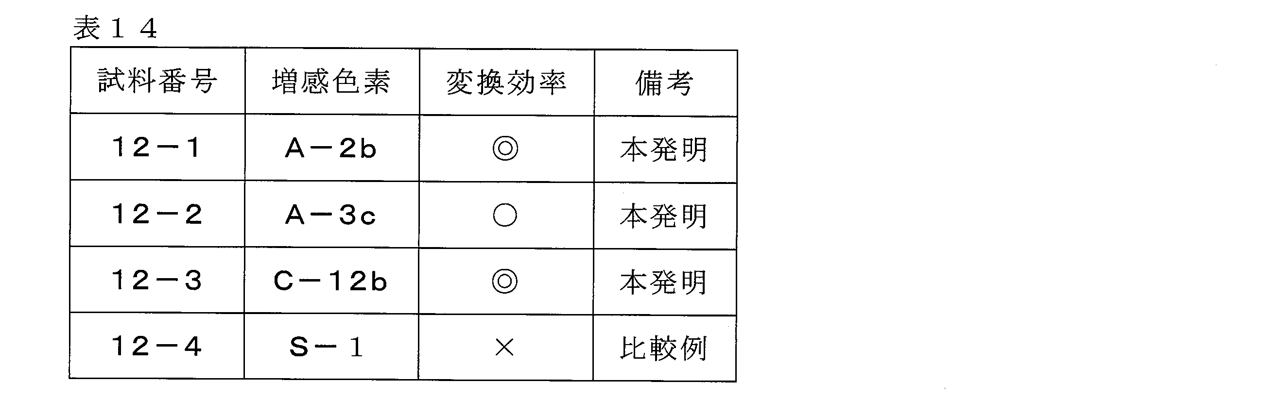
(1)第1光電変換層の形成
市販の酸化チタン粒子(テイカ社製、平均粒径30nm)4.0gとジエチレングリコールモノメチルエーテル20mlとを、硬質ガラスビーズを使用してペイントシェイカーにより6時間分散させ酸化チタン懸濁液を作成した。次いで、この酸化チタン懸濁液をドクターブレードを用いて、予め酸化スズ導電層が付着されたガラス板に塗布し、100℃で30分予備乾燥した後、電気炉で500℃で40分間焼成し、酸化チタン膜を得た。

次に、この溶液中に膜状の酸化チタンを形成した前記のガラス板を入れ、60℃で720分間色素吸着を行ってから乾燥し、第1光電変換層を形成し、試料Aを得た。
市販の酸化ニッケル粒子(キシダ化学社製、平均粒径100nm)4.0gとジエチレングリコールモノメチルエーテル20mlとを、ガラスビーズを使用してペイントシェイカーで8時間分散させ酸化ニッケル懸濁液を作成した。次いで、この酸化ニッケル懸濁液をドクターブレードを用いて、予め酸化スズ導電層が付着されたガラス板に塗布し、100℃で30分予備乾燥した後、電気炉で300℃で30分間焼成し、酸化ニッケル膜を得た。
次に、この溶液中に膜状の酸化ニッケルを形成した前記のガラス板を入れ、70℃で60分間色素吸着を行ってから乾燥し、第2光電変換層を形成し、試料Bを得た。
前記の試料A上に試料Bを位置させる。これら2つの電極の間に液体電解質を入れ、この側面を樹脂で封止した後、リード線を取付けて、光電変換素子(素子構成C)を作成した。なお、液体電解質は、アセトニトリル/炭酸エチレンの混合溶媒(体積比が1:4)に、テトラプロピルアンモニウムアイオダイドとヨウ素とを、それぞれの濃度が0.46mol/L、0.06mol/Lとなるように溶解したものを用いた。
なお、変換効率は、6.5%以上のものを◎、6.0%以上6.5%未満のものを○、5.0%以上6.0%未満のものを△、5.0%未満のものを×として評価した。

高分子電解質を用いた色素増感型光電気化学電池の作製した例について説明する。
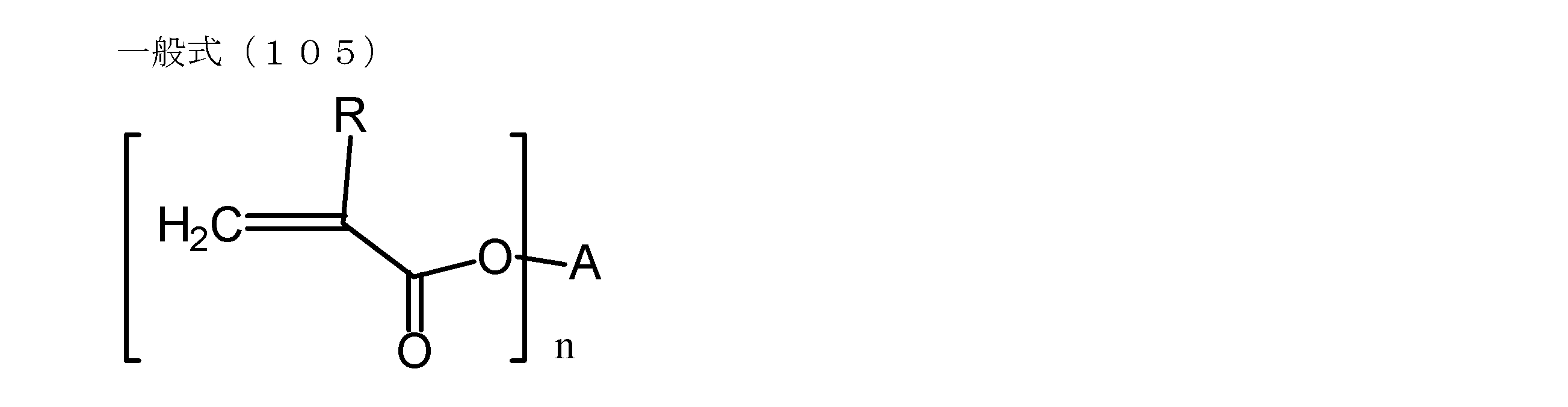
このモノマー単位をプロピレンカーボネート(以下、PCと記載する)に20wt%の濃度で溶解させ、また、熱重合開始剤としてアゾビスイソブチロニトリル(AIBN)をモノマー単位に対して1wt%の濃度で溶解させモノマー溶液を作製する。このモノマー溶液を以下に示す手順に従って、上述の酸化チタン膜に含浸させた。
真空容器内にビーカー等の容器を設置し、その中に透明導電膜を具備した透明基板上の酸化チタン膜Aを入れ、ロータリーポンプで約10分間真空引きする。
真空容器内を真空状態に保ちながらモノマー溶液をビーカー内に注入し、約15分間含浸させ酸化チタン中にモノマー溶液を十分に染み込ます。ポリエチレン製セパレーター、PETフィルムと押さえ板を設置し冶具にて固定する。その後、約85℃で30分間加熱することにより、熱重合させ高分子化合物を作製する。
また、酸化チタン膜を色素吸着後、モノマー処理を行わずに、PCを溶媒として濃度0.5mol/Lのヨウ化リチウムと濃度0.05mol/Lのヨウ素を溶解させて作製した酸化還元電解液をそのまま対極との間に注入して封止して素子Bを作成した。
なお、変換効率は、3.5%以上のものを◎、2.5%以上3.5%未満のものを○、2.0%以上2.5%未満のものを△、2.0%未満のものを×として評価した。

(光電変換素子の作製)
図1に示す光電変換素子10を以下のようにして作製した。
実施例1と同様にして、絶縁性多孔体を形成した受光電極、及び対極として炭素電極を形成した。
次に、下記表17に記載された増感色素(複数混合又は単独)のエタノール溶液に、上記の絶縁性多孔体が形成されたガラス基板を5時間浸漬した。増感色素の染着したガラスを4-tert-ブチルピリジンの10%エタノール溶液に30分間浸漬した後、エタノールで洗浄し自然乾燥させた。このようにして得られる感光体層の厚さは10μmであり、半導体微粒子の塗布量は20g/m2であった。電解液は、ヨウ化ジメチルプロピルイミダゾリウム(0.5mol/L)、ヨウ素(0.1mol/L)のメトキシプロピオニトリル溶液を用いた。
得られた光電気化学電池の変換効率を実験1と同様に測定した。その結果を表17に示す。
なお、変換効率が7.5%以上のものを◎、7.3%以上7.5%未満のものを○、7.1%以上7.3%未満のものを△、7.1%未満のものを×として評価した。
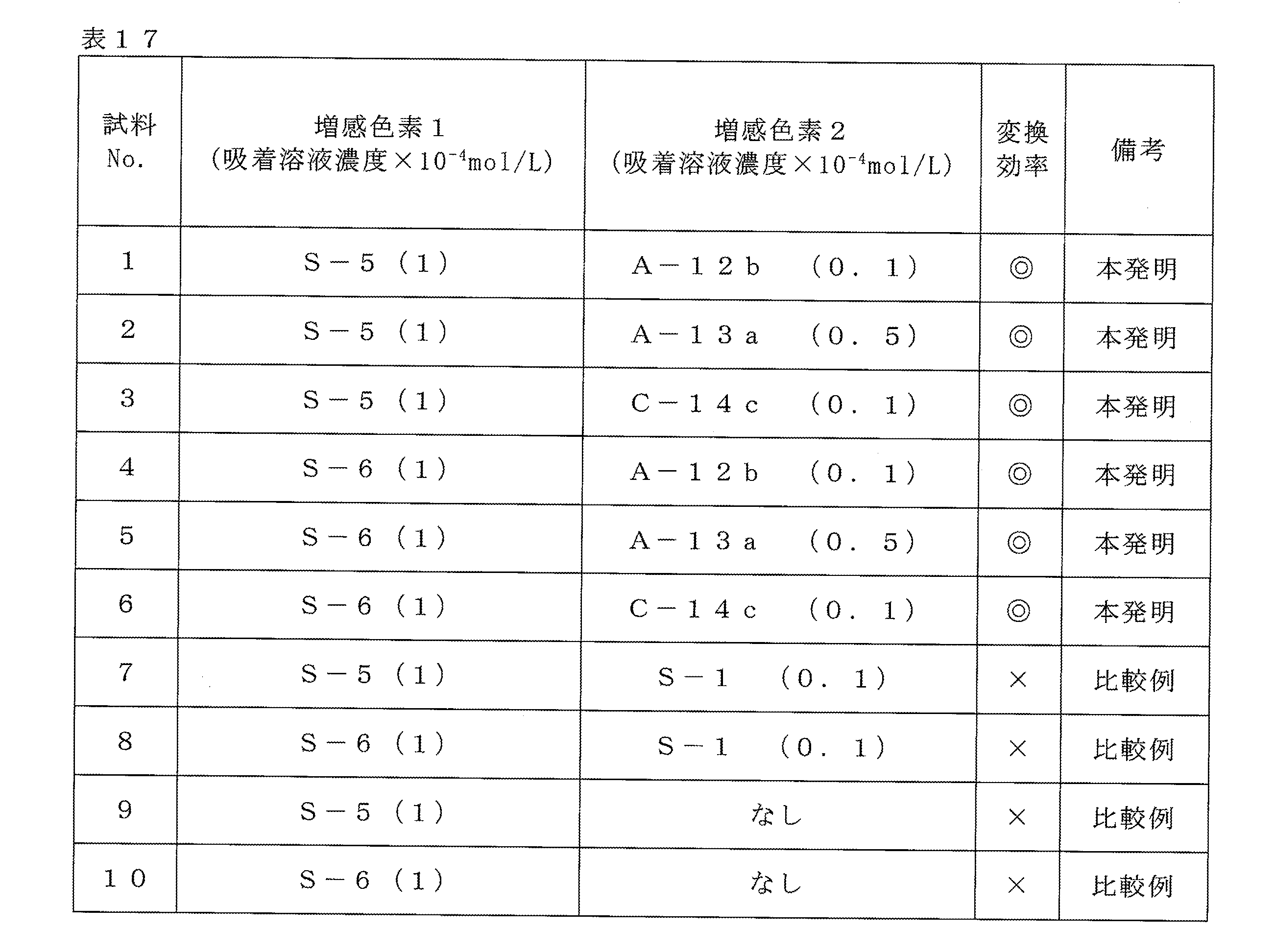

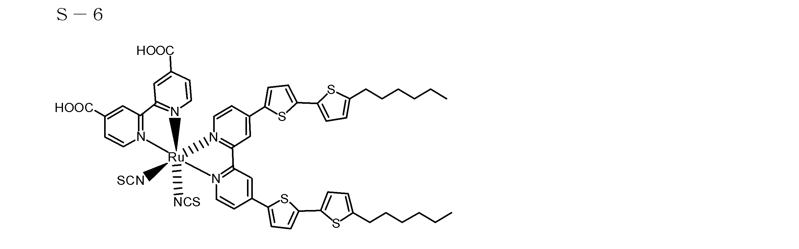
1.電極1Aの作製
酸化チタン微粒子層に吸着させる増感色素を表18に示す増感色素に変えた以外は、実験10と同様にして電極1Aを作製した。
上述のようにして増感色素を吸着させた酸化チタン微粒子層からなる電極1A(20mm×20mm)を同じ大きさの白金蒸着ガラスと重ね合わせた。次に、両ガラスの隙間に毛細管現象を利用して、下記ヘテロ環4級塩化合物を98質量%及びヨウ素を2質量%含有する電解質組成物を浸透させて、電解質を酸化チタン電極中に導入した。これにより、図1に示すように、導電性ガラスからなる導電性支持体1(ガラスの透明基板上に導電層が設層されたもの)、感光体層2、電荷移動体層3、白金からなる対極4及びガラスの透明基板(図示せず)を順に積層し、エピコート828(商品名、ジャパンエポキシレジン社製)、硬化剤及びプラスチックペーストからなる樹脂組成物中に直径25μmのガラス球体がほぼ均一に分散された封止剤で封止した色素増感太陽電池を作製した。ただし、電解質組成物の粘度が高く毛細管現象を利用して電解質組成物を浸透させることが困難な場合は、電解質組成物を50℃に加温し、これを酸化チタン電極に塗布した後、この電極を減圧下に置き電解質組成物が十分浸透し電極中の空気が抜けた後、白金蒸着ガラス(対極)を重ね合わせて同様に色素増感太陽電池を作製した。

500Wのキセノンランプ(ウシオ電機(株)製)の光をAM1.5フィルター(Oriel社製)及びシャープカットフィルター(商品名:Kenko L-37)を通すことにより紫外線を含まない模擬太陽光を発生させた。この光の強度は70mW/cm2であった。この模擬太陽光を、50℃で上記のようにして作製した色素増感太陽電池16-1~16-10に照射し、発生した電気を電流電圧測定装置(ケースレーSMU238型)で測定した。また、85℃で1000時間暗所保存後の変換効率の低下率及び500時間連続光照射後の変換効率の低下率も測定した。これらの結果を表18に示す。

2 感光体層
21 色素
22 半導体微粒子
3 電荷移動体層
4 対極
5 受光電極
6 回路
10 光電変換素子
100 光電気化学電池
Claims (15)
- 下記一般式(1)で表される金属錯体色素。

- 一般式(1)において、前記A~Dの芳香環のうち、酸性基を有する芳香環が、π電子不足系ヘテロ芳香環、又はπ電子不足系ヘテロ芳香環が結合したベンゼン環若しくはナフタレン環である、請求項1記載の金属錯体色素。
- 一般式(1)において、前記A~Dの芳香環のうち、酸性基を有する芳香環の数が、1つ又は2つであることを特徴とする、請求項1又は2記載の金属錯体色素。
- 一般式(1)において、前記A~Dの芳香環のうち、酸性基を有さない芳香環が、それぞれ独立にベンゼン環、ナフタレン環、アントラセン環、フェナントレン環、チオフェン環、又はベンゾチオフェン環である、請求項1~3のいずれか1項記載の金属錯体色素。
- 一般式(1)において、前記酸性基がカルボキシル基であることを特徴とする請求項1~4のいずれか1項記載の金属錯体色素。
- 一般式(1)において、前記酸性基以外のR11~R14で表される置換基が、それぞれ独立に、アルキル基、アリール基、ヘテロ環基、アルキルオキシ基、アルキルチオ基、アルキルシリル基、アリールオキシ基、ヘテロアリールオキシ基、アリールチオ基、ヘテロアリールチオ基又はアリールシリル基、ヘテロアリールシリル基である、請求項1~5のいずれか1項記載の金属錯体色素。
- 一般式(1)において、a11~a14がそれぞれ独立に1~4の整数であることを特徴とする請求項1~6のいずれか1項記載の金属錯体色素。
- 一般式(1)において、Mが、銅、亜鉛、スズ、ニッケル、鉄、コバルト、ケイ素、パラジウム、クロロ-アルミニウム、マグネシウム、ガリウム、チタニルオキシ、又はバナジルオキシである、請求項1~7のいずれか1項記載の金属錯体色素。
- 一般式(1)で表される金属錯体色素が下記一般式(8)又は(9)で表される金属錯体色素である、請求項1~8のいずれか1項記載の金属錯体色素。
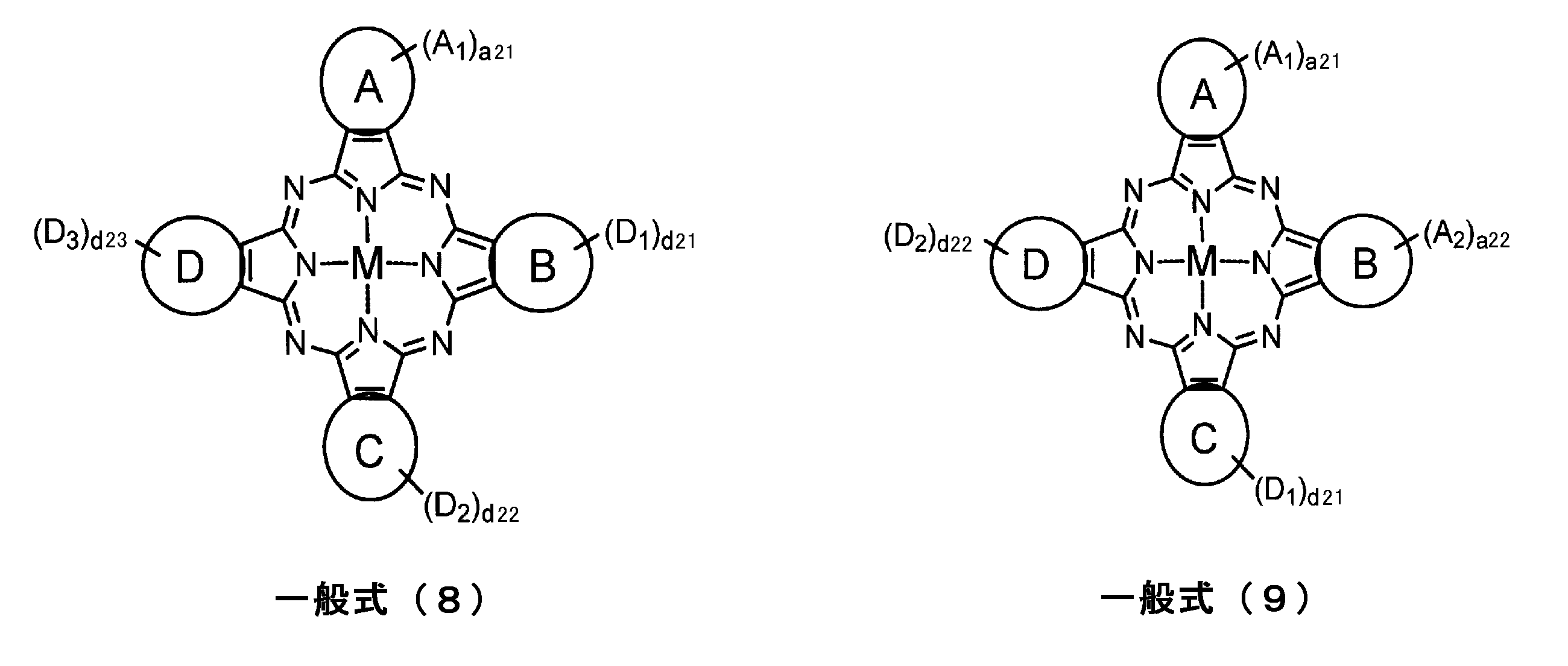
- 請求項1~9のいずれか1項記載の金属錯体色素からなる光電変換素子用色素。
- 請求項1~9のいずれか1項記載の金属錯体色素と半導体微粒子とを有する感光体層を具備した、光電変換素子。
- 前記感光体層が、下記一般式(2)で表される金属錯体色素をさらに含む、請求項11記載の光電変換素子。
Mz(LL1)m1(LL2)m2(X)m3・CI 一般式(2)
[一般式(2)において、Mzは金属原子を表し、LL1は下記一般式(3)で表される2座又は3座の配位子を表し、LL2は下記一般式(4)で表される2座又は3座の配位子を表す。Xはアシルオキシ基、アシルチオ基、チオアシルオキシ基、チオアシルチオ基、アシルアミノオキシ基、チオカルバメート基、ジチオカルバメート基、チオカルボネート基、ジチオカルボネート基、トリチオカルボネート基、アシル基、チオシアネート基、イソチオシアネート基、シアネート基、イソシアネート基、シアノ基、アルキルチオ基、アリールチオ基、アルコキシ基及びアリールオキシ基からなる群から選ばれた基で配位する1座又は2座の配位子、又はハロゲン原子、カルボニル、ジアルキルケトン、1,3-ジケトン、カルボンアミド、チオカルボンアミド及びチオ尿素からなる群より選ばれる1座又は2座の配位子を表す。m1は0~3の整数を表し、m1が2以上のとき、LL1は同じでも異なっていてもよい。m2は1~3の整数を表し、m2が2以上のとき、LL2は同じでも異なっていてもよい。m3は0~3の整数を表し、m3が2以上のとき、Xは同じでも異なっていてもよく、X同士が連結していてもよい。CIは一般式(2)において、電荷を中和させるのに対イオンが必要な場合の対イオンを表す。


- 導電性支持体上に、前記感光体層、電荷移動体及び対極をこの順序で積層した構造を有する、請求項11又は12記載の光電変換素子。
- 前記金属錯体色素が前記半導体微粒子に吸着したことを特徴とする請求項11~13のいずれか1項記載の光電変換素子。
- 請求項11~14のいずれか1項記載の光電変換素子を備えることを特徴とする光電気化学電池。
Priority Applications (2)
| Application Number | Priority Date | Filing Date | Title |
|---|---|---|---|
| JP2012527675A JP5620496B2 (ja) | 2010-08-03 | 2011-07-26 | 金属錯体色素、光電変換素子及び光電気化学電池 |
| CN201180037813.2A CN103124774B (zh) | 2010-08-03 | 2011-07-26 | 金属络合物色素、光电转换元件及光电化学电池 |
Applications Claiming Priority (2)
| Application Number | Priority Date | Filing Date | Title |
|---|---|---|---|
| JP2010174315 | 2010-08-03 | ||
| JP2010-174315 | 2010-08-03 |
Publications (1)
| Publication Number | Publication Date |
|---|---|
| WO2012017868A1 true WO2012017868A1 (ja) | 2012-02-09 |
Family
ID=45559370
Family Applications (1)
| Application Number | Title | Priority Date | Filing Date |
|---|---|---|---|
| PCT/JP2011/067005 Ceased WO2012017868A1 (ja) | 2010-08-03 | 2011-07-26 | 金属錯体色素、光電変換素子及び光電気化学電池 |
Country Status (3)
| Country | Link |
|---|---|
| JP (1) | JP5620496B2 (ja) |
| CN (1) | CN103124774B (ja) |
| WO (1) | WO2012017868A1 (ja) |
Cited By (4)
| Publication number | Priority date | Publication date | Assignee | Title |
|---|---|---|---|---|
| JP2013241502A (ja) * | 2012-05-18 | 2013-12-05 | Nippon Steel & Sumikin Chemical Co Ltd | フタロシアニン色素並びにフタロシアニン色素を用いた色素増感太陽電池及び光電変換素子 |
| GB2503003A (en) * | 2012-06-13 | 2013-12-18 | Dyesol Uk Ltd | Nano-textured Titanium Dioxide powder for use in dye-sensitised solar cells |
| JP2017008194A (ja) * | 2015-06-22 | 2017-01-12 | 山本化成株式会社 | 増感色素、半導体電極、光電変換素子および色素増感太陽電池 |
| KR20200052965A (ko) * | 2017-11-17 | 2020-05-15 | 후지필름 가부시키가이샤 | 광전 변환 소자, 광센서, 촬상 소자, 화합물 |
Families Citing this family (2)
| Publication number | Priority date | Publication date | Assignee | Title |
|---|---|---|---|---|
| KR102013538B1 (ko) * | 2015-09-17 | 2019-08-22 | 후지필름 가부시키가이샤 | 광전 변환 소자, 색소 증감 태양 전지, 색소 조성물 및 산화물 반도체 전극 |
| CN106848065A (zh) * | 2017-02-07 | 2017-06-13 | 晋芳芳 | 一种以金属酞菁化合物作为电子传输层的平面钙钛矿光伏电池 |
Citations (4)
| Publication number | Priority date | Publication date | Assignee | Title |
|---|---|---|---|---|
| JPS6432270A (en) * | 1987-07-28 | 1989-02-02 | Toyo Ink Mfg Co | Planographic printing plate |
| JPH1174003A (ja) * | 1997-06-23 | 1999-03-16 | Sharp Corp | 光電変換材料用光増感剤、光電変換材料およびその製造方法ならびに光電変換装置 |
| WO2010050574A1 (ja) * | 2008-10-29 | 2010-05-06 | 富士フイルム株式会社 | 光電気化学電池 |
| WO2010136178A1 (en) * | 2009-05-26 | 2010-12-02 | Corus Uk Limited | The preparation of a dye compound and a method for making the same |
Family Cites Families (3)
| Publication number | Priority date | Publication date | Assignee | Title |
|---|---|---|---|---|
| US6043428A (en) * | 1997-06-23 | 2000-03-28 | Sharp Kabushiki Kaisha | Photoelectric material using organic photosensitising dyes and manufacturing method thereof |
| CN101384670B (zh) * | 2006-02-10 | 2013-06-05 | 日本化药株式会社 | 四氮杂卟啉色素、油墨、油墨组及着色体 |
| JP5217479B2 (ja) * | 2008-02-13 | 2013-06-19 | コニカミノルタホールディングス株式会社 | 光電変換材料用半導体、光電変換素子及び太陽電池 |
-
2011
- 2011-07-26 JP JP2012527675A patent/JP5620496B2/ja active Active
- 2011-07-26 CN CN201180037813.2A patent/CN103124774B/zh not_active Expired - Fee Related
- 2011-07-26 WO PCT/JP2011/067005 patent/WO2012017868A1/ja not_active Ceased
Patent Citations (4)
| Publication number | Priority date | Publication date | Assignee | Title |
|---|---|---|---|---|
| JPS6432270A (en) * | 1987-07-28 | 1989-02-02 | Toyo Ink Mfg Co | Planographic printing plate |
| JPH1174003A (ja) * | 1997-06-23 | 1999-03-16 | Sharp Corp | 光電変換材料用光増感剤、光電変換材料およびその製造方法ならびに光電変換装置 |
| WO2010050574A1 (ja) * | 2008-10-29 | 2010-05-06 | 富士フイルム株式会社 | 光電気化学電池 |
| WO2010136178A1 (en) * | 2009-05-26 | 2010-12-02 | Corus Uk Limited | The preparation of a dye compound and a method for making the same |
Non-Patent Citations (3)
| Title |
|---|
| ROBERT P. HAMMER ET AL.: "Asymmetrical, Water- Soluble Phthalocyanine Dyes for Covalent Labeling of Oligonucleotides", BIOCONJUGATE CHEMISTRY, vol. 13, 2002, pages 1244 - 1252 * |
| SEUNGHUN EU ET AL.: "Synthesis of sterically hindered phthalocyanines and their applications to dye-sensitized solar cells", DALTON TRANSACTIONS, vol. 40, 2008, pages 5476 - 5483 * |
| XIAOBING WANG ET AL.: "Synthesis, spectral and aggregation properties of a novel water- solublete tracarboxynaphthalocyaninatozinc", DYES AND PIGMENTS, vol. 41, 1999, pages 193 - 198 * |
Cited By (6)
| Publication number | Priority date | Publication date | Assignee | Title |
|---|---|---|---|---|
| JP2013241502A (ja) * | 2012-05-18 | 2013-12-05 | Nippon Steel & Sumikin Chemical Co Ltd | フタロシアニン色素並びにフタロシアニン色素を用いた色素増感太陽電池及び光電変換素子 |
| GB2503003A (en) * | 2012-06-13 | 2013-12-18 | Dyesol Uk Ltd | Nano-textured Titanium Dioxide powder for use in dye-sensitised solar cells |
| GB2503003B (en) * | 2012-06-13 | 2015-07-22 | Dyesol Uk Ltd | Processing titanium dioxide |
| JP2017008194A (ja) * | 2015-06-22 | 2017-01-12 | 山本化成株式会社 | 増感色素、半導体電極、光電変換素子および色素増感太陽電池 |
| KR20200052965A (ko) * | 2017-11-17 | 2020-05-15 | 후지필름 가부시키가이샤 | 광전 변환 소자, 광센서, 촬상 소자, 화합물 |
| KR102430366B1 (ko) | 2017-11-17 | 2022-08-05 | 후지필름 가부시키가이샤 | 광전 변환 소자, 광센서, 촬상 소자, 화합물 |
Also Published As
| Publication number | Publication date |
|---|---|
| CN103124774A (zh) | 2013-05-29 |
| JPWO2012017868A1 (ja) | 2013-10-03 |
| JP5620496B2 (ja) | 2014-11-05 |
| CN103124774B (zh) | 2015-08-19 |
Similar Documents
| Publication | Publication Date | Title |
|---|---|---|
| JP5572029B2 (ja) | 金属錯体色素、光電変換素子及び光電気化学電池 | |
| JP5620316B2 (ja) | 光電変換素子、光電気化学電池及び色素 | |
| JP5620314B2 (ja) | 光電変換素子、光電気化学電池、光電変換素子用色素及び光電変換素子用色素溶液 | |
| JP5681716B2 (ja) | 金属錯体色素、光電変換素子及び光電気化学電池 | |
| JP5925541B2 (ja) | 光電変換素子用金属錯体色素、光電変換素子、色素増感太陽電池、色素増感太陽電池用色素吸着組成液、色素増感太陽電池用半導体電極および色素増感太陽電池の製造方法 | |
| JP5869481B2 (ja) | 金属錯体色素、光電変換素子及び光電気化学電池 | |
| CN103858247A (zh) | 光电转换元件、光电化学电池及其中所使用的金属络合物色素 | |
| JP5721717B2 (ja) | 金属錯体色素、光電変換素子及び光電気化学電池 | |
| JP5620496B2 (ja) | 金属錯体色素、光電変換素子及び光電気化学電池 | |
| JP5689351B2 (ja) | 光電変換素子及び光電気化学電池 | |
| JP5620315B2 (ja) | 光電変換素子及び光電気化学電池 | |
| JP2012053983A (ja) | 光電変換素子及び光電気化学電池 | |
| JP2012051952A (ja) | 色素、光電変換素子及び光電気化学電池 | |
| WO2012017874A1 (ja) | 金属錯体色素、光電変換素子及び光電気化学電池 | |
| WO2012017873A1 (ja) | 金属錯体色素、光電変換素子及び光電気化学電池 | |
| JP5572028B2 (ja) | 光電変換素子及びこれを用いた光電気化学電池、光電変換素子用組成物 | |
| JP2012036239A (ja) | 金属錯体色素、光電変換素子及び光電気化学電池 | |
| JP5756766B2 (ja) | 光電変換素子、光電気化学電池及び色素 | |
| JP5662728B2 (ja) | 色素、これを用いた光電変換素子及び光電気化学電池 | |
| JP2012038436A (ja) | 光電変換素子及びこれを用いた光電気化学電池、光電変換素子用組成物 | |
| JP2012038435A (ja) | 光電変換素子、光電気化学電池及び光電変換素子用色素溶液 | |
| JP5572027B2 (ja) | 光電変換素子及びこれに用いられる光電変換素子用組成物 | |
| JP2011026534A (ja) | 色素、これを用いた光電変換素子及び光電気化学電池 | |
| JP2012038437A (ja) | 光電変換素子及びこれを用いた光電気化学電池、光電変換素子用組成物 | |
| WO2012017870A1 (ja) | 色素、光電変換素子及び光電気化学電池 |
Legal Events
| Date | Code | Title | Description |
|---|---|---|---|
| WWE | Wipo information: entry into national phase |
Ref document number: 201180037813.2 Country of ref document: CN |
|
| 121 | Ep: the epo has been informed by wipo that ep was designated in this application |
Ref document number: 11814496 Country of ref document: EP Kind code of ref document: A1 |
|
| WWE | Wipo information: entry into national phase |
Ref document number: 2012527675 Country of ref document: JP |
|
| NENP | Non-entry into the national phase |
Ref country code: DE |
|
| 122 | Ep: pct application non-entry in european phase |
Ref document number: 11814496 Country of ref document: EP Kind code of ref document: A1 |