WO2012017572A1 - 発振器 - Google Patents
発振器 Download PDFInfo
- Publication number
- WO2012017572A1 WO2012017572A1 PCT/JP2011/001243 JP2011001243W WO2012017572A1 WO 2012017572 A1 WO2012017572 A1 WO 2012017572A1 JP 2011001243 W JP2011001243 W JP 2011001243W WO 2012017572 A1 WO2012017572 A1 WO 2012017572A1
- Authority
- WO
- WIPO (PCT)
- Prior art keywords
- signal
- frequency
- output
- amplifier
- mems
- Prior art date
- Legal status (The legal status is an assumption and is not a legal conclusion. Google has not performed a legal analysis and makes no representation as to the accuracy of the status listed.)
- Ceased
Links
Images








Classifications
-
- H—ELECTRICITY
- H03—ELECTRONIC CIRCUITRY
- H03L—AUTOMATIC CONTROL, STARTING, SYNCHRONISATION OR STABILISATION OF GENERATORS OF ELECTRONIC OSCILLATIONS OR PULSES
- H03L5/00—Automatic control of voltage, current, or power
-
- H—ELECTRICITY
- H03—ELECTRONIC CIRCUITRY
- H03B—GENERATION OF OSCILLATIONS, DIRECTLY OR BY FREQUENCY-CHANGING, BY CIRCUITS EMPLOYING ACTIVE ELEMENTS WHICH OPERATE IN A NON-SWITCHING MANNER; GENERATION OF NOISE BY SUCH CIRCUITS
- H03B19/00—Generation of oscillations by non-regenerative frequency multiplication or division of a signal from a separate source
-
- H—ELECTRICITY
- H03—ELECTRONIC CIRCUITRY
- H03L—AUTOMATIC CONTROL, STARTING, SYNCHRONISATION OR STABILISATION OF GENERATORS OF ELECTRONIC OSCILLATIONS OR PULSES
- H03L1/00—Stabilisation of generator output against variations of physical values, e.g. power supply
- H03L1/02—Stabilisation of generator output against variations of physical values, e.g. power supply against variations of temperature only
- H03L1/022—Stabilisation of generator output against variations of physical values, e.g. power supply against variations of temperature only by indirect stabilisation, i.e. by generating an electrical correction signal which is a function of the temperature
- H03L1/026—Stabilisation of generator output against variations of physical values, e.g. power supply against variations of temperature only by indirect stabilisation, i.e. by generating an electrical correction signal which is a function of the temperature by using a memory for digitally storing correction values
-
- H—ELECTRICITY
- H03—ELECTRONIC CIRCUITRY
- H03L—AUTOMATIC CONTROL, STARTING, SYNCHRONISATION OR STABILISATION OF GENERATORS OF ELECTRONIC OSCILLATIONS OR PULSES
- H03L1/00—Stabilisation of generator output against variations of physical values, e.g. power supply
- H03L1/02—Stabilisation of generator output against variations of physical values, e.g. power supply against variations of temperature only
- H03L1/022—Stabilisation of generator output against variations of physical values, e.g. power supply against variations of temperature only by indirect stabilisation, i.e. by generating an electrical correction signal which is a function of the temperature
- H03L1/027—Stabilisation of generator output against variations of physical values, e.g. power supply against variations of temperature only by indirect stabilisation, i.e. by generating an electrical correction signal which is a function of the temperature by using frequency conversion means which is variable with temperature, e.g. mixer, frequency divider, pulse add/subtract logic circuit
-
- H—ELECTRICITY
- H03—ELECTRONIC CIRCUITRY
- H03L—AUTOMATIC CONTROL, STARTING, SYNCHRONISATION OR STABILISATION OF GENERATORS OF ELECTRONIC OSCILLATIONS OR PULSES
- H03L7/00—Automatic control of frequency or phase; Synchronisation
- H03L7/06—Automatic control of frequency or phase; Synchronisation using a reference signal applied to a frequency- or phase-locked loop
- H03L7/16—Indirect frequency synthesis, i.e. generating a desired one of a number of predetermined frequencies using a frequency- or phase-locked loop
- H03L7/18—Indirect frequency synthesis, i.e. generating a desired one of a number of predetermined frequencies using a frequency- or phase-locked loop using a frequency divider or counter in the loop
Definitions
- the technical field relates to oscillators, and in particular, to oscillators using MEMS resonators.
- an oscillator is used for timing (synchronizing) the operation of a circuit in an electronic device or the like.
- An oscillator that accurately outputs an electrical signal serving as a reference for operation is an indispensable device for electronic equipment.
- a crystal oscillator using a crystal resonator is an example of such an oscillator, but the crystal oscillator is difficult to miniaturize, unsuitable for integration, has a large number of prototypes, and has a poor yield.
- We have problems such as time required for delivery. Therefore, in recent years, an oscillator using a micro electro-mechanical system (MEMS) produced by a semiconductor process from silicon or the like has attracted attention as a device replacing a crystal oscillator.
- MEMS micro electro-mechanical system
- a micro electro mechanical oscillator (hereinafter referred to as “MEMS oscillator”) includes a feedback oscillation circuit including an amplifier circuit and a MEMS resonator.
- the MEMS resonator has a characteristic that the electric passing characteristic between the input and output electrodes is remarkably improved only for an electric signal having a frequency in the vicinity of a specific frequency, that is, a resonance frequency of the MEMS vibrator (natural frequency of the vibrator).
- a resonance frequency of the MEMS vibrator naturally frequency of the vibrator.
- the MEMS oscillator outputs an electrical signal output from the amplifier circuit as an oscillation signal in the oscillation state. Therefore, the frequency of the oscillation signal output from the MEMS oscillator is determined based on the resonance frequency of the MEMS vibrator.
- the MEMS resonator is generally formed of silicon or the like, and has a temperature characteristic of about ⁇ 20 [ppm / ° C.] at the resonance frequency due to the temperature characteristic of silicon. For example, if the operating temperature changes by 100 ° C. from ⁇ 20 to + 80 ° C., the resonance frequency changes by about 2000 [ppm]. Therefore, when the operating temperature of the MEMS resonator changes, the frequency of the oscillation signal also changes.
- a temperature sensor is arranged in the vicinity of the MEMS resonator, and based on the temperature measured by the temperature sensor, the frequency variation of the oscillation signal due to the temperature dependence of the resonance frequency of the MEMS resonator is compensated. It outputs an electric signal with a constant frequency regardless of the temperature.
- FIG. 21 is a block diagram of a conventional MEMS oscillator.
- the conventional MEMS oscillator 300 includes an oscillation unit 301 that outputs an original oscillation signal, and a correction unit 302 that corrects the frequency of the original oscillation signal and outputs an output signal having a desired frequency (see Patent Document 1). .
- the feedback type oscillation circuit is configured by the amplifier 312 and the MEMS resonator 313, and an output from the amplifier 312 is extracted as an original oscillation signal and input to the correction unit 302.
- the correction unit 302 keeps the frequency of the output signal constant by compensating for the variation in the frequency of the original oscillation signal.
- the correction unit 302 includes a PLL (Phase-Locked Loop) circuit 321, a frequency division ratio control unit 322 that controls a frequency division ratio of a frequency divider (not shown) provided in the feedback of the PLL circuit 321, and a temperature sensor 1101. Is provided.
- PLL Phase-Locked Loop
- the frequency division ratio control unit 322 is based on the input from the temperature sensor 1101, and the frequency division ratio of a frequency divider (not shown) provided in the feedback of the PLL 321 so that the frequency of the output signal output from the PLL 321 becomes a desired value. Adjust. More specifically, the frequency division ratio control unit 322 uses the temperature characteristics of the resonance frequency of the known MEMS resonator 313, the input from the temperature sensor 1101, and the frequency of the preset output signal as feedback of the PLL 321. A frequency dividing ratio of the arranged frequency divider (not shown) is determined.
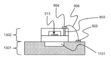
- FIG. 22 is a side sectional view of the MEMS resonator 300 described above.
- the MEMS resonator 313 is packaged so that the periphery of the vibrator is kept in vacuum so that air or the like does not affect the mechanical vibration of the vibrator.
- the MEMS resonator 313 having such a structure is formed as a second chip 1302 that is different from the first chip 1301 in which the amplification unit 312 and the correction unit 302 are formed.
- the temperature sensor 1101 is formed in the vicinity of the MEMS resonator 313 in the first chip 1301.
- the first chip 1301 and the second chip 1302 are connected to the pad 804 connected to the wiring 803 extending from the exterior surface of the second chip 1302 to the surface layer of the circuit, and to the first chip 1301.
- the pads 805 are connected by connecting them with metal wires 806 and mounted in a vertical stack.
- the periphery of the vibrator of the MEMS resonator 313 is in a vacuum state. Therefore, the thermal conductivity between the vibrator and the outside thereof is low. However, there is a difference between the time variation of the temperature measured by the temperature sensor 1101 of the first chip 1301 and the time variation of the actual temperature of the vibrator of the MEMS resonator 313.
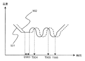
- FIG. 23 is a diagram schematically showing an example of the time change of the temperature measured by the temperature sensor 1101 and the actual temperature of the vibrator in the MEMS resonator 313.
- the actual temperature 902 of the vibrator fluctuates so as to follow the temperature 901 with a slight delay from the temperature 901.
- the temperature 901 measured by the temperature sensor 1101 coincides with the actual temperature 902 of the vibrator only at a very limited time such as the period D903 and times T904, T905, and T906. It does not match.
- the temperature dependence of the resonance frequency of the MEMS resonator 313 is correctly compensated in real time based on the actual temperature of the vibrator, and a frequency that exactly matches the desired frequency is obtained. It is difficult to always output the output signal that it has.
- the correction unit includes a frequency synthesizer including a programmable frequency divider that can variably control the frequency division ratio, and a frequency division ratio control unit that controls the frequency division ratio of the programmable frequency divider.
- the frequency division ratio control unit controls the frequency division ratio of the programmable frequency divider based on the information signal, and the frequency synthesizer inputs the original oscillation signal, generates a signal of a predetermined set frequency from the original oscillation signal, and outputs it It may be output as a signal.
- the information signal may be a feedback signal from the MEMS resonator to the amplifier.
- the information signal may be a control signal for controlling the gain of the amplifier output from the automatic gain controller.
- the automatic gain controller compares the peak hold circuit that receives the original oscillation signal and detects the peak voltage of the original oscillation signal with the predetermined reference voltage and compares the peak voltage. And an automatic gain controller that outputs a signal indicating the result of comparison as a control signal to control the gain of the amplifier.
- the correction unit may further include a second frequency divider that inputs the original oscillation signal, divides the original oscillation signal, and outputs the divided signal to the frequency synthesizer.
- the second frequency divider may be a second programmable frequency divider.
- the frequency division ratio control unit may control the frequency division ratio of the second programmable frequency divider based on the information signal.
- the correction unit may further include a multiplier that inputs the original oscillation signal, multiplies the original oscillation signal, and outputs the multiplied signal to the frequency synthesizer.
- the multiplier may be a programmable multiplier.
- the frequency division ratio control unit may control the multiplication ratio of the programmable multiplier based on the information signal.
- the MEMS oscillator according to the present embodiment can stably output an electric signal having a desired frequency even when the temperature of the MEMS resonator fluctuates.
- Block diagram of the MEMS oscillator of the first embodiment Diagram of frequency characteristics of output of MEMS resonator Automatic gain controller block diagram
- Block diagram of division ratio control unit Block diagram of another example of division ratio control unit Diagram of temperature characteristics of output of MEMS resonator Diagram of frequency characteristics of output of MEMS resonator Figure of temperature characteristics of output voltage of MEMS resonator Block diagram of the MEMS oscillator of the second embodiment
- the figure which shows the relationship between the output of a MEMS resonator, and the output of an amplifier The figure which shows the relationship between the output of a MEMS resonator, and the output of an amplifier
- the MEMS oscillator includes a feedback oscillation circuit including a MEMS resonator, an amplifier, and an automatic gain controller that controls the gain of the amplifier so as to keep the output from the amplifier constant.
- the correction unit of the MEMS oscillator includes a PLL frequency synthesizer that inputs an original oscillation signal and outputs an output signal, and a frequency division ratio of a programmable frequency divider arranged in the feedback of the PLL frequency synthesizer.
- a frequency division ratio control unit that controls based on the gain.
- the correction unit controls the frequency division ratio of the programmable frequency divider based on the magnitude of the gain of the MEMS resonator, and maintains the frequency of the output signal from the frequency synthesizer at a desired frequency.
- the frequency division ratio control unit receives a signal fed back from the MEMS resonator to the amplifier, and acquires the gain of the MEMS resonator from the level of the signal.
- the frequency division ratio control unit receives a control signal (amplitude limiting signal) that is output from the automatic gain controller and controls the gain of the amplifier so as to keep the output level from the amplifier constant.
- the gain of the MEMS resonator is obtained from the amplitude control signal.
- the MEMS oscillator corrects the fluctuation of the frequency of the original oscillation signal due to the temperature dependence of the resonance frequency of the MEMS resonator, and outputs an output signal having a constant desired frequency. Is possible.
- FIG. 1 is a block diagram of a MEMS oscillator according to the first embodiment.
- the MEMS oscillator 100 includes an oscillation unit 1 that outputs an original oscillation signal and a correction unit 2 that receives the original oscillation signal and outputs an output signal having a desired frequency.
- the oscillation unit 1 includes an automatic gain controller 11, an amplifier 12 that amplifies an input signal (oscillation unit feedback signal) to a certain level (voltage) under the control of the automatic gain controller 11, and an amplifier 12 And an MEMS resonator 13 that returns an oscillation unit feedback signal to the amplifier 12.
- the automatic gain controller 11 inputs the output from the amplifier 12 and controls the gain of the amplifier 12 so as to keep the output level of the amplifier 12 constant.
- the control signal used for the control is referred to as an amplitude limit signal.
- the amplifier 12 receives the feedback signal from the MEMS resonator 13 and amplifies and outputs the feedback signal under gain control by the amplitude limiting signal input from the automatic gain controller 11.
- An output (original oscillation signal) from the amplifier 12 is sent to the automatic gain controller 11, the correction unit 2, and the MEMS resonator 13.
- the MEMS resonator 13 receives an output from the amplifier 12 and outputs a feedback signal.
- the feedback signal from the MEMS resonator 13 to the amplifier 12 is particularly referred to as an oscillation unit feedback signal. To do.
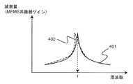
- FIG. 2 is a graph showing the electrical passage characteristics (single passage characteristics) between the input and output electrodes of the MEMS resonator 13.
- the horizontal axis represents frequency and the vertical axis represents attenuation (MEMS resonator gain).
- MEMS resonator gain When the MEMS resonator 13 receives an input of an appropriate level, the MEMS resonator 13 exhibits a pass characteristic 401 that is symmetrical with respect to the resonance frequency f. However, when the MEMS resonator 13 receives an excessive level of input, the MEMS resonator 13 exhibits a distorted pass characteristic like the pass characteristic 402.
- the automatic gain controller 11 controls the gain of the amplifier 12 so that the output of the amplifier 12 becomes an appropriate level for the MEMS resonator 13 so that an excessive level signal is not input to the MEMS resonator 13.
- the output of the amplifier 12 is kept at a predetermined level.
- An appropriate level as an input to the MEMS resonator 13 is the resonance mode of the MEMS resonator 13, the gap interval between the vibrator and the excitation electrode constituting the MEMS resonator 13, the vibrator and / or the excitation electrode. It is determined from an applied bias voltage or the like, and is generally about several tens to several hundred millivolts.
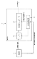
- FIG. 3 is a block diagram showing details of the automatic gain controller 11.
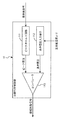
- An automatic gain controller (AGC) 11 receives an output from the amplifier 12, that is, an original oscillation signal, and a peak hold circuit 111 detects the maximum level (peak voltage) of the original oscillation signal.
- the automatic gain controller 11 receives a reference voltage from a reference voltage source (not shown) via a reference voltage input terminal 112. The peak voltage and the reference voltage are input to the comparator 113.
- the comparator 113 compares both voltages, and when the peak voltage is lower than the reference voltage, the amplitude limit signal “Low” is output. When the voltage is higher than the reference voltage, the amplitude limit signal “High” is output.
- the amplitude limiting signal output from the automatic gain controller 11 is input to, for example, the gate of a MOS (Metal Oxide Semiconductor) transistor arranged in parallel with the output terminal of the amplifier 12.
- MOS Metal Oxide Semiconductor
- the parallel resistance decreases, and the gain of the amplifier 12 increases.
- the amplitude limit signal “High” is input to the gate, the parallel resistance increases.
- the gain of the amplifier 12 is reduced.
- the automatic gain controller 11 controls the output level from the amplifier 12 in real time based on the reference voltage. By doing so, the level of the output from the amplifier 12 (input to the MEMS resonator 13) is always kept at an appropriate level, and normal operation of the MEMS resonator 13 is ensured.
- the circuit comprised from the peak hold circuit 111 and the comparator 113 was mentioned as a structural example of the automatic gain controller 11, this is an example and the structure of the automatic gain controller 11 is not restricted to this. Absent. Any circuit that can control the gain of the amplifier 12 so that the output level (voltage) from the amplifier 12 is constant can be used as the automatic gain controller 11.
- a circuit that controls the amplifier 12 by specifically specifying the gain value of the amplifier 12 as the amplitude limiting signal may be used.
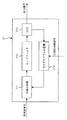
- FIG. 4 is a block diagram showing details of the frequency synthesizer 21 of the correction unit 2.
- the frequency synthesizer 21 is a PLL frequency synthesizer.
- the phase comparator 211 receives an original oscillation signal input from the oscillation unit 1 and a feedback signal (PLL feedback signal) fed back from the VCO (Voltage Controlled Oscillator) 213 via the programmable frequency divider 214. ) And the detected phase difference is output to the loop filter 212 as an error signal.
- the loop filter 212 removes an unnecessary short period (high frequency) fluctuation component included in the error signal and outputs it to the VCO 213 as a correction signal.
- the VCO 213 controls the frequency of the output signal according to the level (voltage) of the input correction signal, and outputs an output signal having a frequency corresponding to the level of the correction signal.
- Programmable frequency divider 214 is a frequency divider that can variably set the frequency dividing ratio in accordance with external control.
- the frequency division ratio of the programmable frequency divider 214 is set according to the frequency division controlled signal output from the frequency division ratio control unit 22.
- the frequency division ratio control unit 22 receives the oscillation unit feedback signal of the MEMS resonator 13, acquires the gain of the MEMS resonator 13 from the level (voltage) of the oscillation unit feedback signal, and the MEMS resonator. The operation of controlling the frequency division ratio of the programmable frequency divider 214 based on the gain of 13 will be described.
- FIG. 5 is a graph showing the temperature characteristics of the resonance frequency of the MEMS resonator 13.
- the resonance frequency here corresponds to the peak frequency f in the pass characteristic 401 in FIG.
- the resonance frequency of the MEMS resonator 13 has a temperature dependency of about ⁇ 20 [ppm / ° C.].
- the resonance frequency of the MEMS resonator 13 monotonously decreases as the temperature rises. Note that the MEMS oscillators of the present embodiment and the following second embodiment are applicable even when the resonance frequency of the resonator increases monotonously with a temperature rise.
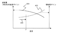
- FIG. 6 is a graph showing the temperature characteristics of the attenuation amount (MEMS resonator gain) of the MEMS resonator 13. As shown in the figure, the attenuation amount of the MEMS resonator 13 also has a temperature characteristic 404 that monotonously decreases as the temperature rises.
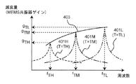
- FIG. 7 is a graph showing the correspondence between the resonance frequency and the gain of the MEMS resonator 13.
- T TH.
- the gain of the MEMS resonator 13 at that time is gTH.
- the pass characteristics 401M and L where the temperatures TH, TM, and TL have a relationship of TH> TM> TL.
- a curve 403 is obtained by connecting a resonance frequency (fTH, fTM, fTL) at each temperature and a gain of a resonance frequency at another temperature (not shown).
- a curve 403 is a curve showing the correspondence between the resonance frequency and the gain of the MEMS resonator 13.
- the output level from the amplifier 12 is always kept constant by the action of the automatic gain controller 11. Therefore, the level of the feedback signal from the MEMS resonator 13 corresponds to the gain of the MEMS resonator 13. Therefore, the level of the feedback signal from the MEMS resonator 13 shows a temperature characteristic like a curve 601 shown in FIG. For example, if the operating temperature is TL, the MEMS resonator 13 outputs a feedback signal including the frequency component of the frequency fTL having the level (voltage) VTL, and the level of the frequency component is the peak voltage of the feedback signal. Really match. The same applies to other temperatures.
- the frequency division ratio control unit 22 receives the oscillation unit feedback signal (original oscillation frequency information signal) from the MEMS resonator 13 and detects the maximum level (peak voltage) of the oscillation unit feedback signal. Then, based on the peak voltage and the resonance frequency-gain correspondence shown in FIG. 7, the resonance frequency of the MEMS resonator 13 at that time is derived. That is, the oscillation unit feedback signal (original oscillation frequency information signal) is an information signal including information related to the gain of the MEMS resonator 13. The frequency division ratio control unit 22 derives a resonance frequency from the information signal.
- the frequency division ratio to be set in the programmable frequency divider 214 is determined from the derived resonance frequency and the frequency of the preset output signal, and the frequency division ratio of the programmable frequency divider 214 is determined.
- a frequency division ratio control signal for setting the frequency ratio is output to the programmable frequency division ratio 214.
- FIG. 9 is a block diagram illustrating an example of the frequency division ratio control unit 22.
- the signal generator 221 receives the original oscillation frequency information signal (oscillator feedback signal), detects the peak voltage, and stores a table indicating the correspondence between the peak voltage and the frequency division ratio of the programmable frequency divider 214.
- the frequency division ratio to be set in the programmable frequency divider 214 is determined with reference to the table memory 222.
- the frequency division ratio control unit 22 may include a peak hold circuit in order to detect the peak voltage of the original oscillation frequency information signal.
- the MEMS oscillator 100 changes the frequency of the original oscillation signal that varies due to temperature variation or the like to the correspondence between the gain of the MEMS resonator 13 and the resonance frequency. Based on this, an output signal having a preset frequency can be output.
- the MEMS oscillator 100 according to the present embodiment can acquire the gain of the MEMS resonator 13 in real time using a signal generated by the MEMS resonator 13 itself, and can correct the frequency of the original oscillation signal. That is, the gain of the MEMS resonator 13 (the level of the oscillation unit feedback signal) can be used as information regarding the operating temperature of the MEMS resonator 13.
- the operation temperature is obtained from the gain of the MEMS resonator 13, the resonance frequency of the MEMS resonator 13 at that time is obtained from the temperature characteristics of the resonance frequency, the operation of the frequency synthesizer 21 is controlled, and a desired An output signal having a frequency is output.
- the MEMS resonator 100 does not require a temperature sensor as in the conventional configuration. Therefore, a deviation from the set value of the frequency of the output signal due to a deviation between the measured temperature of the temperature sensor and the actual operating temperature of the vibrator does not occur in the MEMS oscillator 100. However, the MEMS oscillator 100 can always stably output a high-quality output signal.
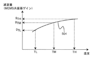
- the MEMS resonator 13 having the gain temperature characteristic 504 as shown in FIG. 11 can constitute the MEMS oscillator 100 of the present embodiment.
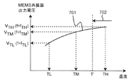
- the correspondence relationship between the resonance frequency and the gain of the MEMS resonator 13 is a curve that monotonously decreases as the temperature rises, as a curve 503 shown in FIG. Therefore, the level of the oscillation unit feedback signal from the MEMS resonator 13 changes as shown by a curve 701 shown in FIG. 13 as the temperature changes.
- the configuration of a PLL frequency synthesizer using an analog PLL circuit is shown as the frequency synthesizer 21.
- the frequency synthesizer 21 is not limited to an analog PLL circuit, and is a digital PLL circuit or an all-digital one. You may comprise using a PLL circuit. Further, the frequency synthesizer 21 may have a circuit configuration other than the PLL circuit.
- the programmable frequency divider 214 of the PLL frequency synthesizer 21 of the present embodiment may be configured using either an integer type frequency divider or a fractional type frequency divider.
- FIG. 14 is a block diagram of the MEMS oscillator according to the second embodiment. Constituent elements equivalent to those of the MEMS oscillator 100 of the first embodiment are denoted by the same reference numerals, and description thereof will be omitted as appropriate.
- the MEMS oscillator 200 uses the amplitude limit signal output from the automatic gain controller 11 as the original oscillation frequency information signal.
- the amplitude limit signal is a signal used to control the amplifier 12 to keep its gain constant.
- FIG. 15 is a graph showing the relationship between the gain 404 of the MEMS resonator 13 and the gain 405 of the amplifier 12 along the operating temperature of the MEMS resonator 13.
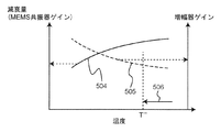
- the gain 405 of the amplifier 12 and the gain 404 of the MEMS resonator 13 have a one-to-one correspondence. That is, the amplitude limit signal (original oscillation frequency information signal) is an information signal including a signal having a corresponding relationship with the gain at the resonance frequency of the MEMS resonator 13. Therefore, it is possible to acquire the gain of the MEMS resonator 13 by monitoring an amplitude limit signal that is a signal for controlling the gain of the amplifier 12.
- the frequency division ratio control unit 22 inputs the amplitude limit signal as an original oscillation frequency information signal, detects the gain of the MEMS resonator 13 based on the signal, and the resonance frequency of the MEMS resonator 13 as shown in FIG. Deriving the resonance frequency of the MEMS resonator 13 at that time from the gain correspondence. Then, the frequency division ratio control unit 22 determines the frequency division ratio to be set in the programmable frequency divider 214 as in the first embodiment.
- the MEMS resonator 13 having the gain temperature characteristic 504 as shown in FIG. 16 can constitute the MEMS oscillator 200 of the present embodiment.
- the correspondence relationship between the gain of the MEMS resonator 13 and the gain of the amplifier 12 is a curve that monotonously decreases as the temperature rises, as a curve 505 shown in FIG.
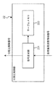
- FIG. 17 is a diagram illustrating a first modification of the correction unit 2 that can be applied to the MEMS oscillators 100 and 200.
- a frequency divider 31 that divides the frequency of the original oscillation signal by 1 / R is disposed in front of the PLL frequency synthesizer 21.
- the frequency of the original oscillation signal and the frequency of the output signal are of the same order. Even in this case, the frequency of the original oscillation signal can be precisely corrected.
- the frequency divider 31 is configured by a second programmable frequency divider
- the frequency division ratio control unit 22 is configured to control the frequency division ratio of the frequency divider 31. Also good.
- the correction unit 2 can precisely correct the frequency of the original oscillation signal to an arbitrary real number frequency under the control of the frequency division ratio control unit 22.
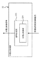
- FIG. 18 is a diagram illustrating a second modification of the correction unit 2 that can be applied to the MEMS oscillators 100 and 200.
- a multiplier 32 that multiplies the frequency of the original oscillation signal by R is disposed in front of the PLL frequency synthesizer 21.
- the frequency of the output signal is sufficiently smaller than the frequency of the original oscillation signal.
- the frequency of the original oscillation signal can be precisely corrected.
- the multiplier 32 may be configured by a programmable multiplier, and the frequency division ratio control unit 22 may be configured to control the multiplication ratio of the multiplier 32. Also in this case, the correction unit 2 can precisely correct the frequency of the original oscillation signal to an arbitrary real number frequency under the control of the frequency division ratio control unit 22.
- the correction unit 2 may further include a frequency divider or a multiplier in the subsequent stage of the PLL frequency synthesizer 21 (on the side where the output of the VCO 213 is input).
- FIG. 19 is a diagram illustrating a modification of the MEMS oscillator 100 according to the first embodiment.
- the MEMS oscillator modification 1100 includes a temperature sensor 1101 in addition to the configuration of the MEMS oscillator 100.
- the output of the temperature sensor 1101 is input to the frequency division ratio control unit 22.
- the frequency division ratio control unit 22 may generate a frequency division ratio control signal using the output of the temperature sensor 1101 below the predetermined temperature T.
- the MEMS oscillator 1100 can stably output a high-quality output signal even in a temperature region in which fluctuation due to a temperature change in the output level of the MEMS resonator 13 is relatively small.
- the frequency division ratio control unit 22 may generate a frequency division ratio control signal using the output of the temperature sensor 1101.
- FIG. 20 is a diagram illustrating a modification of the MEMS oscillator 200 according to the second embodiment.
- the MEMS oscillator modification 1200 includes a temperature sensor 1101 in addition to the configuration of the MEMS oscillator 200.
- the output of the temperature sensor 1101 is input to the frequency division ratio control unit 22.
- the frequency division ratio control unit 22 may generate a frequency division ratio control signal using the output of the temperature sensor 1101. By doing so, the MEMS oscillator 1100 can stably output a high-quality output signal even in a temperature region in which fluctuation due to a temperature change of the amplifier 12 is relatively small.
- the frequency division ratio control unit 22 may generate a frequency division ratio control signal using the output of the temperature sensor 1101.
- the MEMS oscillator includes a feedback oscillation circuit including a MEMS resonator, an amplifier, and an automatic gain controller that controls the gain of the amplifier so as to keep the output from the amplifier constant.
- the correction unit includes a frequency synthesizer and a frequency division ratio control unit that controls the frequency division ratio of the programmable frequency divider arranged in the feedback of the frequency synthesizer based on the gain of the MEMS resonator.
- the frequency division ratio control unit determines the frequency division ratio of the programmable frequency divider based on the magnitude of the gain of the MEMS resonator.
- the magnitude of the gain of the MEMS resonator has temperature dependence and changes monotonously as the temperature changes. Therefore, the resonance frequency of the MEMS resonator and the magnitude of the gain have a one-to-one correspondence relationship in which one can be uniquely determined from the other. Therefore, the resonance frequency at that time can be known from the magnitude of the gain of the MEMS resonator.
- the frequency division ratio control unit controls the frequency division ratio of the programmable frequency divider based on the correspondence relationship in real time in response to the time variation of the gain of the MEMS resonator. By doing so, the time variation of the frequency of the original oscillation signal is accurately corrected in real time, and an output signal having a frequency that matches the desired frequency is always output from the MEMS oscillator.
- the frequency division ratio control unit can receive a signal fed back from the MEMS resonator to the amplifier and acquire the gain of the MEMS resonator from the level of the signal. Because, in the oscillation unit, the output from the amplifier is always kept constant by the action of the automatic gain controller, so the level (voltage) of the feedback signal of the MEMS resonator corresponds well with the gain of the MEMS resonator. It is.
- the frequency division ratio control unit monitors a control signal (amplitude limit signal) output from the automatic gain controller for controlling the gain of the amplifier so as to keep the output level from the amplifier constant. It is possible to obtain the gain of the MEMS resonator. This is because in the oscillating unit, the automatic gain controller outputs an amplitude control signal so as to keep the output from the amplifier at a constant level. Therefore, the level of the signal fed back from the MEMS resonator to the amplifier (that is, the gain of the MEMS resonator) can be known from the amplitude control signal.
- the MEMS oscillators according to the first and second embodiments described above sufficiently correct the fluctuation in the frequency of the original oscillation signal due to the temperature dependence of the resonance frequency of the MEMS resonator, and always output an output signal having a desired frequency stably. Is possible.
- the output signal output from the MEMS oscillator according to the present embodiment has a stable frequency at all times, it is useful for applications such as a clock generator.
Landscapes
- Oscillators With Electromechanical Resonators (AREA)
- Stabilization Of Oscillater, Synchronisation, Frequency Synthesizers (AREA)
- Inductance-Capacitance Distribution Constants And Capacitance-Resistance Oscillators (AREA)
Abstract
Description
1.MEMS発振器の構成
図1は、実施の形態1にかかるMEMS発振器のブロック図である。MEMS発振器100は、原発振信号を出力する発振部1と、原発振信号を受けて所望の周波数を有する出力信号を出力する補正部2と、を有する。
2.1発振部の動作
図2は、MEMS共振器13の入出力電極間の電気通過特性(単体通過特性)を示すグラフである。同図において横軸は周波数を示し、縦軸は減衰量(MEMS共振器ゲイン)を示す。MEMS共振器13は、適切なレベルの入力を受けた場合には、共振周波数fについて左右対称な通過特性401を示す。しかし、MEMS共振器13は、過大なレベルの入力を受けた場合には、通過特性402のように歪んだ通過特性を示す。そのような過大なレベルの入力をMEMS共振器13が受けると、MEMS共振器13の共振周波数は変化するとともに、不安定化する。併せて、Q値も劣化し、場合によっては、MEMS共振器13を構成する振動子がギャップを隔てて隣接する励振電極と接触し、MEMS共振器13は破壊される。そこで、MEMS共振器13に対し過大なレベルの信号が入力されないように、自動利得制御器11は、増幅器12の出力がMEMS共振器13にとって適切なレベルになるように増幅器12のゲインを制御し、増幅器12の出力を所定のレベルに保つ。なお、MEMS共振器13への入力として適切なレベルは、MEMS共振器13の共振モードや、MEMS共振器13を構成する振動子と励振電極とのギャップ間隔や、振動子および/または励振電極に印加されるバイアス電圧などから決定され、一般的にはおおよそ数十から数百ミリボルト程度である。
図4は、補正部2の周波数シンセサイザ21の詳細を示すブロック図である。周波数シンセサイザ21は、PLL周波数シンセサイザである。周波数シンセサイザ21では、先ずその位相比較器211が、発振部1から入力される原発振信号と、VCO(Voltage Controlled Oscillator)213からプログラマブル分周器214を介して帰還される帰還信号(PLL帰還信号)の位相差を検出し、検出した位相差を誤差信号としてループフィルタ212へ出力する。ループフィルタ212は、誤差信号に含まれる不要な短周期(高周波数)の変動成分を除去し、補正信号としてVCO213へ出力する。VCO213は、入力される補正信号のレベル(電圧)にしたがって出力信号の周波数を制御し、補正信号のレベルに対応した周波数の出力信号を出力する。
プログラマブル分周器214は、外部からの制御にしたがいその分周比を可変的に設定可能な分周器である。補正部2においては、プログラマブル分周器214の分周比は、分周比制御部22が出力する分周被制御信号にしたがって設定される。以下、分周比制御部22が、MEMS共振器13の発振部帰還信号を受けて、当該発振部帰還信号のレベル(電圧)の大きさからMEMS共振器13のゲインを取得し、MEMS共振器13のゲインに基づいてプログラマブル分周器214の分周比を制御する動作について説明する。
このようにして、本実施の形態のMEMS発振器100は、温度変動等に起因して変動する原発振信号の周波数を、MEMS共振器13のゲインと共振周波数との対応関係に基づいて補正し、予め設定された周波数を有する出力信号を出力することができる。本実施の形態のMEMS発振器100は、MEMS共振器13自身が発する信号を用いてリアルタイムにMEMS共振器13のゲインを取得し、原発振信号の周波数の補正を行うことが可能になっている。つまり、MEMS共振器13のゲイン(発振部帰還信号のレベル)は、MEMS共振器13の動作温度に関する情報として用いることができる。そこで、MEMS発振器100においては、MEMS共振器13のゲインから動作温度を求め、共振周波数の温度特性からそのときのMEMS共振器13の共振周波数を求め、周波数シンセサイザ21の動作を制御し、所望の周波数を有する出力信号を出力する。
図14は、実施の形態2にかかるMEMS発振器のブロック図である。実施の形態1のMEMS発振器100と同等の構成要素については同様の参照数字を付し、その説明を適宜省略する。
図17は、MEMS発振器100および200に適用可能な、補正部2の第1の変形例を示す図である。本変形例においては、PLL周波数シンセサイザ21の前段に、原発振信号の周波数を1/Rに分周する分周器31が配置される。このように、分周器31を用いて原発振信号の周波数を分周してからPLL周波数シンセサイザ21へ入力することにより、原発振信号の周波数と出力信号の周波数とが同程度のオーダである場合でも、原発振信号の周波数の補正を精緻に行うことが可能になる。また、同図において破線で示すように、分周器31を第2のプログラマブル分周器で構成し、分周比制御部22が分周器31の分周比を制御するように構成してもよい。この場合、補正部2は、分周比制御部22の制御の下、原発振信号の周波数を任意の実数倍の周波数に精緻に補正することが可能である。
図18は、MEMS発振器100および200に適用可能な、補正部2の第2の変形例を示す図である。本変形例においては、PLL周波数シンセサイザ21の前段に、原発振信号の周波数をR倍する逓倍器32が配置される。このように、逓倍器32を用いて原発振信号の周波数を逓倍してからPLL周波数シンセサイザ21へ入力することにより、原発振信号の周波数の周波数に較べて出力信号の周波数が十分小さいような場合でも、原発振信号の周波数の補正を精緻に行うことが可能になる。また、変形例1と同様、破線で示すように、逓倍器32をプログラマブル逓倍器で構成し、分周比制御部22が逓倍器32の逓倍比を制御するように構成してもよい。この場合も、補正部2は、分周比制御部22の制御の下、原発振信号の周波数を任意の実数倍の周波数に精緻に補正することが可能である。
図19は、実施の形態1によるMEMS発振器100の変形例を示す図である。MEMS発振器変形例1100は、MEMS発振器100の構成に加え、温度センサ1101を有する。温度センサ1101の出力は、分周比制御部22へ入力される。
図20は、実施の形態2によるMEMS発振器200の変形例を示す図である。MEMS発振器変形例1200は、MEMS発振器200の構成に加え、温度センサ1101を有する。温度センサ1101の出力は、分周比制御部22へ入力される。
本実施の形態のMEMS発振器は、MEMS共振器と、増幅器と、増幅器からの出力を一定に保つように増幅器のゲインを制御する自動利得制御器と、で構成された帰還型発振回路を備えた発振部、および、発振部から出力される原発振信号から所望の周波数の出力信号を生成して出力する補正部、を有する。
2 補正部
11 自動利得制御器
12 増幅器
13 MEMS共振器
21 周波数シンセサイザ
22 分周比制御部
111 ピークホールド回路
112 基準電圧入力端子
113 コンパレータ
211 位相比較器
212 ループフィルタ
213 電圧制御発振器
214 プログラマブル分周器
221 信号生成部
222 テーブルメモリ
223 信号生成部
224 分周比演算部
Claims (9)
- MEMS共振器と増幅器とを含んだ帰還型発振回路、および、前記増幅器からの出力を受けて該出力のレベルに基づいて前記増幅器からの出力のレベルを一定に保つように前記増幅器のゲインを制御する自動利得制御器を備え、前記増幅器からの出力を原発振信号として出力する発振部と、
前記原発振信号を入力し前記原発振信号から所定の設定周波数の信号を生成し出力信号として出力する補正部と、を有し、
前記補正部は、前記原発振信号とは別に、前記MEMS共振器の共振周波数におけるゲインと対応関係を有する信号を含む情報信号を前記発振部から入力し、前記情報信号に基づいて前記原発振信号の周波数を補正して前記所定の設定周波数の信号を生成し出力信号として出力する、MEMS発振器。 - 前記補正部は、分周比を可変的に制御可能なプログラマブル分周器を備えた周波数シンセサイザと、前記プログラマブル分周器の分周比を制御する分周比制御部と、を備え、
前記分周比制御部は、前記情報信号に基づいて前記プログラマブル分周器の分周比を制御し、前記周波数シンセサイザは、前記原発振信号を入力し前記原発振信号から前記所定の設定周波数の信号を生成し出力信号として出力する、請求項1に記載のMEMS発振器。 - 前記情報信号は、前記MEMS共振器から前記増幅器への帰還信号である、請求項1に記載のMEMS発振器。
- 前記情報信号は、前記自動利得制御器が出力する前記増幅器のゲインを制御するための制御信号である、請求項1に記載のMEMS発振器。
- 前記自動利得制御器は、前記原発振信号を入力して前記原発振信号のピーク電圧を検出するピークホールド回路と、前記検出にかかるピーク電圧と所定の基準電圧とを比較し、該比較の結果を示す信号を出力するコンパレータと、を備え、
前記自動利得制御器は、前記制御信号として前記比較の結果を示す信号を出力して前記増幅器のゲインを制御する、請求項1に記載のMEMS発振器。 - 前記補正部は、さらに、前記原発振信号を入力し該原発振信号を分周して前記周波数シンセサイザへ出力する第2の分周器を備える、請求項2に記載のMEMS発振器。
- 前記第2の分周器は、第2のプログラマブル分周器であり、
前記分周比制御部は、前記情報信号に基づいて前記第2のプログラマブル分周器の分周比を制御する、請求項6に記載のMEMS発振器。 - 前記補正部は、さらに、前記原発振信号を入力し該原発振信号を逓倍して前記周波数シンセサイザへ出力する逓倍器を備える、請求項2に記載のMEMS発振器。
- 前記逓倍器は、プログラマブル逓倍器であり、
前記分周比制御部は、前記情報信号に基づいて前記プログラマブル逓倍器の逓倍比を制御する、請求項8に記載のMEMS発振器。
Priority Applications (3)
| Application Number | Priority Date | Filing Date | Title |
|---|---|---|---|
| US13/322,263 US8525605B2 (en) | 2010-08-06 | 2011-03-03 | Oscillator |
| JP2011544742A JP5086479B2 (ja) | 2010-08-06 | 2011-03-03 | 発振器 |
| CN201180001810.3A CN102439844B (zh) | 2010-08-06 | 2011-03-03 | 振荡器 |
Applications Claiming Priority (2)
| Application Number | Priority Date | Filing Date | Title |
|---|---|---|---|
| JP2010177556 | 2010-08-06 | ||
| JP2010-177556 | 2010-08-06 |
Publications (1)
| Publication Number | Publication Date |
|---|---|
| WO2012017572A1 true WO2012017572A1 (ja) | 2012-02-09 |
Family
ID=45559098
Family Applications (1)
| Application Number | Title | Priority Date | Filing Date |
|---|---|---|---|
| PCT/JP2011/001243 Ceased WO2012017572A1 (ja) | 2010-08-06 | 2011-03-03 | 発振器 |
Country Status (4)
| Country | Link |
|---|---|
| US (1) | US8525605B2 (ja) |
| JP (1) | JP5086479B2 (ja) |
| CN (1) | CN102439844B (ja) |
| WO (1) | WO2012017572A1 (ja) |
Cited By (3)
| Publication number | Priority date | Publication date | Assignee | Title |
|---|---|---|---|---|
| JP2015126286A (ja) * | 2013-12-25 | 2015-07-06 | セイコーエプソン株式会社 | 発振回路、発振器、電子機器、移動体及び発振器の製造方法 |
| JP2016535491A (ja) * | 2013-10-28 | 2016-11-10 | クゥアルコム・インコーポレイテッドQualcomm Incorporated | リアルタイムクロックアプリケーションのための超低電力高周波数水晶発振器 |
| US9523909B2 (en) | 2011-09-04 | 2016-12-20 | Maradin Technologies Ltd. | Apparatus and methods for locking resonating frequency of a miniature system |
Families Citing this family (11)
| Publication number | Priority date | Publication date | Assignee | Title |
|---|---|---|---|---|
| US8821009B2 (en) * | 2009-12-23 | 2014-09-02 | Intel Corporation | Thermal sensors having flexible substrates and use thereof |
| US8570112B2 (en) * | 2011-06-09 | 2013-10-29 | Panasonic Corporation | Oscillator with MEMS resonator |
| US8884711B2 (en) * | 2012-09-24 | 2014-11-11 | Invensense, Inc. | MEMS device oscillator loop with amplitude control |
| US8803622B1 (en) * | 2012-09-28 | 2014-08-12 | Integrated Device Technology, Inc | Microelectromechanical-based oscillators having adjustable gain amplifiers therein that support Q-factor control |
| US9621170B2 (en) * | 2013-08-13 | 2017-04-11 | Silicon Laboratories Inc. | Accurate frequency control using a MEMS-based oscillator |
| CN105375921A (zh) * | 2014-08-27 | 2016-03-02 | 硅谷实验室公司 | 使用基于mems的振荡器的准确频率控制 |
| US9543891B2 (en) * | 2015-04-09 | 2017-01-10 | Texas Instruments Incorporated | Low-power low-phase-noise oscillator |
| US9866336B2 (en) * | 2015-06-17 | 2018-01-09 | Google Llc | Phased array antenna self-calibration |
| US10243518B2 (en) * | 2016-09-12 | 2019-03-26 | Avago Technologies International Sales Pte. Limited | Single input, dual output path low-noise amplifier |
| JP6372545B2 (ja) * | 2016-11-14 | 2018-08-15 | 横河電機株式会社 | 振動式トランスデューサ |
| CN113765516B (zh) * | 2021-09-10 | 2024-01-12 | 中国航空工业集团公司西安飞行自动控制研究所 | 一种mems谐振器闭环控制方法及控制结构 |
Citations (3)
| Publication number | Priority date | Publication date | Assignee | Title |
|---|---|---|---|---|
| JP2007518351A (ja) * | 2004-01-09 | 2007-07-05 | ロベルト・ボッシュ・ゲゼルシャフト・ミト・ベシュレンクテル・ハフツング | 周波数および/または位相補償された微細電気機械発振器 |
| WO2009101791A1 (ja) * | 2008-02-14 | 2009-08-20 | Panasonic Corporation | シンセサイザと、これを用いた受信装置 |
| JP2009200888A (ja) * | 2008-02-22 | 2009-09-03 | Seiko Instruments Inc | Mems発振器 |
Family Cites Families (11)
| Publication number | Priority date | Publication date | Assignee | Title |
|---|---|---|---|---|
| JPH06276088A (ja) * | 1993-03-24 | 1994-09-30 | Matsushita Electric Ind Co Ltd | システム時計回路 |
| US5495206A (en) * | 1993-10-29 | 1996-02-27 | Motorola, Inc. | Fractional N frequency synthesis with residual error correction and method thereof |
| US6052036A (en) * | 1997-10-31 | 2000-04-18 | Telefonaktiebolaget L M Ericsson | Crystal oscillator with AGC and on-chip tuning |
| JP2001014057A (ja) * | 1999-07-02 | 2001-01-19 | Nec Yonezawa Ltd | 温度管理機能搭載クロックジェネレータ |
| US6278338B1 (en) * | 2000-05-01 | 2001-08-21 | Silicon Wave Inc. | Crystal oscillator with peak detector amplitude control |
| EP1432119A1 (en) * | 2002-12-17 | 2004-06-23 | Dialog Semiconductor GmbH | High quality serial resonance oscillator |
| JP2007208584A (ja) * | 2006-02-01 | 2007-08-16 | Ricoh Co Ltd | 周波数調整回路 |
| US20070257728A1 (en) * | 2006-05-03 | 2007-11-08 | Sitime Corporation | Microelectromechanical multi-stage oscillator |
| JP5205827B2 (ja) | 2007-06-14 | 2013-06-05 | 日本電気株式会社 | 発振周波数制御方法及び発振器 |
| US8044736B2 (en) * | 2008-04-29 | 2011-10-25 | Sand9, Inc. | Timing oscillators and related methods |
| JP4822139B2 (ja) * | 2008-08-04 | 2011-11-24 | セイコーエプソン株式会社 | 機器及び機器の製造方法 |
-
2011
- 2011-03-03 CN CN201180001810.3A patent/CN102439844B/zh not_active Expired - Fee Related
- 2011-03-03 US US13/322,263 patent/US8525605B2/en not_active Expired - Fee Related
- 2011-03-03 JP JP2011544742A patent/JP5086479B2/ja not_active Expired - Fee Related
- 2011-03-03 WO PCT/JP2011/001243 patent/WO2012017572A1/ja not_active Ceased
Patent Citations (3)
| Publication number | Priority date | Publication date | Assignee | Title |
|---|---|---|---|---|
| JP2007518351A (ja) * | 2004-01-09 | 2007-07-05 | ロベルト・ボッシュ・ゲゼルシャフト・ミト・ベシュレンクテル・ハフツング | 周波数および/または位相補償された微細電気機械発振器 |
| WO2009101791A1 (ja) * | 2008-02-14 | 2009-08-20 | Panasonic Corporation | シンセサイザと、これを用いた受信装置 |
| JP2009200888A (ja) * | 2008-02-22 | 2009-09-03 | Seiko Instruments Inc | Mems発振器 |
Cited By (3)
| Publication number | Priority date | Publication date | Assignee | Title |
|---|---|---|---|---|
| US9523909B2 (en) | 2011-09-04 | 2016-12-20 | Maradin Technologies Ltd. | Apparatus and methods for locking resonating frequency of a miniature system |
| JP2016535491A (ja) * | 2013-10-28 | 2016-11-10 | クゥアルコム・インコーポレイテッドQualcomm Incorporated | リアルタイムクロックアプリケーションのための超低電力高周波数水晶発振器 |
| JP2015126286A (ja) * | 2013-12-25 | 2015-07-06 | セイコーエプソン株式会社 | 発振回路、発振器、電子機器、移動体及び発振器の製造方法 |
Also Published As
| Publication number | Publication date |
|---|---|
| US20120182077A1 (en) | 2012-07-19 |
| JP5086479B2 (ja) | 2012-11-28 |
| CN102439844A (zh) | 2012-05-02 |
| JPWO2012017572A1 (ja) | 2013-09-19 |
| CN102439844B (zh) | 2015-02-11 |
| US8525605B2 (en) | 2013-09-03 |
Similar Documents
| Publication | Publication Date | Title |
|---|---|---|
| JP5086479B2 (ja) | 発振器 | |
| JP5204354B1 (ja) | 発振器 | |
| US7990229B2 (en) | Methods and devices for compensating a signal using resonators | |
| US7595701B2 (en) | Crystal oscillator | |
| TWI684327B (zh) | 調整時脈訊號中之工作周期的裝置與方法 | |
| US8674772B2 (en) | Oscillating signal generator utilized in phase-locked loop and method for controlling the oscillating signal generator | |
| CN101652928B (zh) | 振荡频率控制电路 | |
| US11239844B2 (en) | Oscillator | |
| CN101490960B (zh) | 振荡频率控制电路及其校正方法 | |
| JP6564244B2 (ja) | 発振装置および発振装置の製造方法 | |
| JP5253318B2 (ja) | 発振装置 | |
| JP2014175981A (ja) | 発振器 | |
| JP2002026658A (ja) | 水晶発振回路 | |
| JP2015061171A (ja) | 発振装置 | |
| JP2015119378A (ja) | 高安定発振器 | |
| JP5918546B2 (ja) | 温度補償型水晶発振器 | |
| WO2021205695A1 (ja) | 可変容量素子及びそれを備えた発振器 | |
| JP6707366B2 (ja) | 発振装置 | |
| US12218631B2 (en) | Circuit apparatus and oscillator | |
| US12388403B2 (en) | Circuit device and oscillator | |
| JP4314982B2 (ja) | 温度補償型圧電発振器 | |
| JP2025104473A (ja) | 回路装置及び発振器 | |
| JP2015119212A (ja) | 発振器 | |
| JP2015170997A (ja) | 温度補償型発振デバイス及び温度補償型圧電発振器 | |
| JP2025114091A (ja) | 回路装置及び発振器 |
Legal Events
| Date | Code | Title | Description |
|---|---|---|---|
| WWE | Wipo information: entry into national phase |
Ref document number: 201180001810.3 Country of ref document: CN |
|
| WWE | Wipo information: entry into national phase |
Ref document number: 2011544742 Country of ref document: JP |
|
| WWE | Wipo information: entry into national phase |
Ref document number: 13322263 Country of ref document: US |
|
| 121 | Ep: the epo has been informed by wipo that ep was designated in this application |
Ref document number: 11814212 Country of ref document: EP Kind code of ref document: A1 |
|
| NENP | Non-entry into the national phase |
Ref country code: DE |
|
| 122 | Ep: pct application non-entry in european phase |
Ref document number: 11814212 Country of ref document: EP Kind code of ref document: A1 |