WO2012014904A1 - Euvリソグラフィ用反射層付基板、およびeuvリソグラフィ用反射型マスクブランク - Google Patents
Euvリソグラフィ用反射層付基板、およびeuvリソグラフィ用反射型マスクブランク Download PDFInfo
- Publication number
- WO2012014904A1 WO2012014904A1 PCT/JP2011/066993 JP2011066993W WO2012014904A1 WO 2012014904 A1 WO2012014904 A1 WO 2012014904A1 JP 2011066993 W JP2011066993 W JP 2011066993W WO 2012014904 A1 WO2012014904 A1 WO 2012014904A1
- Authority
- WO
- WIPO (PCT)
- Prior art keywords
- layer
- film
- reflective
- euv
- protective layer
- Prior art date
- Legal status (The legal status is an assumption and is not a legal conclusion. Google has not performed a legal analysis and makes no representation as to the accuracy of the status listed.)
- Ceased
Links
Images

Classifications
-
- H—ELECTRICITY
- H10—SEMICONDUCTOR DEVICES; ELECTRIC SOLID-STATE DEVICES NOT OTHERWISE PROVIDED FOR
- H10P—GENERIC PROCESSES OR APPARATUS FOR THE MANUFACTURE OR TREATMENT OF DEVICES COVERED BY CLASS H10
- H10P76/00—Manufacture or treatment of masks on semiconductor bodies, e.g. by lithography or photolithography
- H10P76/20—Manufacture or treatment of masks on semiconductor bodies, e.g. by lithography or photolithography of masks comprising organic materials
- H10P76/204—Manufacture or treatment of masks on semiconductor bodies, e.g. by lithography or photolithography of masks comprising organic materials of organic photoresist masks
- H10P76/2041—Photolithographic processes
-
- G—PHYSICS
- G03—PHOTOGRAPHY; CINEMATOGRAPHY; ANALOGOUS TECHNIQUES USING WAVES OTHER THAN OPTICAL WAVES; ELECTROGRAPHY; HOLOGRAPHY
- G03F—PHOTOMECHANICAL PRODUCTION OF TEXTURED OR PATTERNED SURFACES, e.g. FOR PRINTING, FOR PROCESSING OF SEMICONDUCTOR DEVICES; MATERIALS THEREFOR; ORIGINALS THEREFOR; APPARATUS SPECIALLY ADAPTED THEREFOR
- G03F1/00—Originals for photomechanical production of textured or patterned surfaces, e.g., masks, photo-masks, reticles; Mask blanks or pellicles therefor; Containers specially adapted therefor; Preparation thereof
- G03F1/22—Masks or mask blanks for imaging by radiation of 100nm or shorter wavelength, e.g. X-ray masks, extreme ultraviolet [EUV] masks; Preparation thereof
- G03F1/24—Reflection masks; Preparation thereof
-
- B—PERFORMING OPERATIONS; TRANSPORTING
- B82—NANOTECHNOLOGY
- B82Y—SPECIFIC USES OR APPLICATIONS OF NANOSTRUCTURES; MEASUREMENT OR ANALYSIS OF NANOSTRUCTURES; MANUFACTURE OR TREATMENT OF NANOSTRUCTURES
- B82Y10/00—Nanotechnology for information processing, storage or transmission, e.g. quantum computing or single electron logic
-
- B—PERFORMING OPERATIONS; TRANSPORTING
- B82—NANOTECHNOLOGY
- B82Y—SPECIFIC USES OR APPLICATIONS OF NANOSTRUCTURES; MEASUREMENT OR ANALYSIS OF NANOSTRUCTURES; MANUFACTURE OR TREATMENT OF NANOSTRUCTURES
- B82Y40/00—Manufacture or treatment of nanostructures
-
- G—PHYSICS
- G02—OPTICS
- G02B—OPTICAL ELEMENTS, SYSTEMS OR APPARATUS
- G02B5/00—Optical elements other than lenses
- G02B5/08—Mirrors
- G02B5/0891—Ultraviolet [UV] mirrors
-
- G—PHYSICS
- G03—PHOTOGRAPHY; CINEMATOGRAPHY; ANALOGOUS TECHNIQUES USING WAVES OTHER THAN OPTICAL WAVES; ELECTROGRAPHY; HOLOGRAPHY
- G03F—PHOTOMECHANICAL PRODUCTION OF TEXTURED OR PATTERNED SURFACES, e.g. FOR PRINTING, FOR PROCESSING OF SEMICONDUCTOR DEVICES; MATERIALS THEREFOR; ORIGINALS THEREFOR; APPARATUS SPECIALLY ADAPTED THEREFOR
- G03F1/00—Originals for photomechanical production of textured or patterned surfaces, e.g., masks, photo-masks, reticles; Mask blanks or pellicles therefor; Containers specially adapted therefor; Preparation thereof
- G03F1/22—Masks or mask blanks for imaging by radiation of 100nm or shorter wavelength, e.g. X-ray masks, extreme ultraviolet [EUV] masks; Preparation thereof
Definitions
- the present invention relates to a reflective mask blank (hereinafter referred to as “EUV mask blank”) for EUV (Extreme Ultraviolet) lithography used in semiconductor manufacturing and the like, and the production of the EUV mask blank.
- EUV mask blank for EUV (Extreme Ultraviolet) lithography used in semiconductor manufacturing and the like
- the present invention relates to a substrate with a reflective layer for EUV lithography used, and an EUV mask obtained by patterning the EUV mask blank.
- the resolution limit of the pattern is about 1 ⁇ 2 of the exposure wavelength, and it is said that the immersion wavelength is about 1 ⁇ 4 of the exposure wavelength, and the ArF laser (wavelength: 193 nm) is used. Even if the immersion method is used, the exposure wavelength is expected to be about 45 nm.
- EUV lithography which is an exposure technique using EUV light having a shorter wavelength than that of an ArF laser, is promising as a next-generation exposure technique using an exposure wavelength shorter than 45 nm.
- EUV light refers to light having a wavelength in the soft X-ray region or vacuum ultraviolet region, and specifically refers to light having a wavelength of about 10 to 20 nm, particularly about 13.5 nm ⁇ 0.3 nm.
- a conventional refractive optical system such as photolithography using visible light or ultraviolet light may be used. Can not. For this reason, in the EUV light lithography, a reflective optical system, that is, a reflective photomask and a mirror are used.
- the mask blank is a laminated body before patterning used for photomask manufacturing.
- a reflective layer that reflects EUV light and an absorber layer that absorbs EUV light are formed in this order on a glass substrate or the like.
- the produced Mo / Si multilayer reflective film is usually used.
- a reflective layer formed by alternately laminating a plurality of silicon (Si) layers that are high refractive layers and molybdenum (Mo) layers that are low refractive layers is referred to as a Mo / Si multilayer reflective film.
- a material having a high absorption coefficient for EUV light specifically, a material mainly composed of chromium (Cr) or tantalum (Ta) is used.
- a protective layer is usually formed between the reflective layer and the absorber layer.
- the protective layer is provided for the purpose of protecting the reflective layer so that the reflective layer is not damaged by an etching process performed for the purpose of patterning the absorber layer.
- Patent Document 1 proposes the use of ruthenium (Ru) as a material for the protective layer.
- Patent Document 2 proposes a protective layer made of a ruthenium compound (Ru content of 10 to 95 at%) containing Ru and at least one selected from Mo, Nb, Zr, Y, B, Ti, and La. Has been.
- the protective layer When Ru is used as the material for the protective layer, a high etching selectivity with respect to the absorber layer can be obtained, and even when the protective layer is formed on the reflective layer, a high etching selectivity is obtained when the protective layer surface is irradiated with EUV light. Reflectance is obtained.
- the steps performed when manufacturing the mask blank and the steps performed when manufacturing the photomask from the mask blank for example, cleaning, defect inspection, heating step, dry etching
- the protective layer is oxidized by oxidizing the Ru protective layer and further the uppermost layer of the multilayer reflective film (in the case of a Mo / Si multilayer reflective film).
- the protective layer described in Patent Document 2 is described as being capable of sufficiently obtaining the anti-oxidation effect of the multilayer reflective film without causing a decrease in the reflectance of the multilayer reflective film.
- the decrease in the reflectance is caused by the Si layer and the Ru protective layer, which are the uppermost layers of the multilayer reflective film, during the Ru protective layer film formation or the subsequent heat treatment or the like.
- Si layer and the Ru protective layer which are the uppermost layers of the multilayer reflective film, during the Ru protective layer film formation or the subsequent heat treatment or the like.
- the EUV light reflectivity is reduced by oxidation of the Ru protective layer as described above.
- the present invention provides an EUV mask blank in which a decrease in EUV light reflectance due to oxidation of a Ru protective layer is suppressed, and a substrate with a functional film used for manufacturing the EUV mask blank. With the goal.
- the present inventors have found that a first layer containing a predetermined amount of nitrogen and Si between the Mo / Si multilayer reflective film and the Ru protective layer, and Ru, It has been found that a decrease in EUV light reflectance due to oxidation of the Ru protective layer can be suppressed by forming a two-layer intermediate layer comprising a second layer containing a predetermined amount of nitrogen and Si.
- the present invention has been made based on the above-mentioned findings of the present inventors, and an EUV in which a reflective layer that reflects EUV light and a protective layer that protects the reflective layer are formed on a substrate in this order.
- a substrate with a reflective layer for lithography The reflective layer is a Mo / Si multilayer reflective film;
- the protective layer is a Ru layer or a Ru compound layer;
- a second layer containing 0.1 to 10 at% nitrogen and 0.1 to 30 at% Si, and the total thickness of the first layer and the second layer is 0.2 to 2.5 nm.
- the first layer constituting the intermediate layer is formed on the reflective layer side, the second layer is formed on the first layer, Provided is a substrate with a reflective layer for EUV lithography (hereinafter also referred to as “the substrate with a reflective layer of the present invention”), wherein the protective layer contains substantially no Si.
- the thickness of the first layer of the intermediate layer is 0.1 to 2.4 nm
- the thickness of the second layer is 0.1 to 2.4 nm
- the difference in film thickness between the second layer and the first layer is preferably 0 to 2.3 nm.
- the surface roughness (rms) of the surface of the protective layer is preferably 0.5 nm or less.
- the surface roughness (rms) means the root mean square surface roughness and is also referred to as the surface roughness Rq.
- the protective layer preferably has a thickness of 1 to 10 nm.
- the present invention is a reflective mask blank for EUV lithography in which an absorber layer is formed on the protective layer of the above-described substrate with a reflective layer of the present invention (hereinafter also referred to as “EUV mask blank of the present invention”). I will provide a.
- the absorber layer is preferably formed of a material mainly composed of tantalum (Ta).
- the etching selectivity between the protective layer and the absorber layer when dry etching is performed using a chlorine-based gas as an etching gas is preferably 10 or more.
- a low reflection layer for inspection light used for inspection of a mask pattern which is formed of a material mainly containing tantalum (Ta), is provided on the absorber layer. preferable.
- the reflected light on the surface of the protective layer with respect to the wavelength of light used for the inspection of the pattern formed on the absorber layer, and the surface on the surface of the low reflection layer is preferably 30% or more.
- the present invention also provides a reflective mask for EUV lithography (hereinafter also referred to as “the EUV mask of the present invention”) obtained by patterning the EUV mask blank of the present invention described above.
- the present invention also provides a method for manufacturing a semiconductor integrated circuit, wherein a semiconductor integrated circuit is manufactured by exposing an object to be exposed using the EUV mask of the present invention described above.
- a semiconductor integrated circuit is manufactured by exposing an object to be exposed using the EUV mask of the present invention described above.
- “to” is used in the sense that numerical values described before and after it are included as a lower limit value and an upper limit value.
- the EUV mask produced by using the EUV mask blank of the present invention is a highly reliable EUV mask in which the EUV light reflectance changes little with time during EUV exposure.
- FIG. 1 is a schematic cross-sectional view showing an embodiment of an EUV mask blank of the present invention.
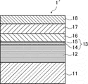
- FIG. 2 is a view similar to FIG. However, a low reflection layer is formed on the absorber layer.
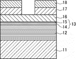
- FIG. 3 shows a state in which a pattern is formed on the absorber layer 17 (and the low reflection layer 18) of the EUV mask blank 1 ′ of FIG.
- FIG. 1 is a schematic cross-sectional view showing an embodiment of the EUV mask blank of the present invention.
- a mask blank 1 shown in FIG. 1 includes a reflective layer 12 that reflects EUV light on a substrate 11 and a protective layer 16 that protects the reflective layer 12 in this order.
- a first layer 14 containing a predetermined amount of nitrogen and Si, which will be described later, and Ru, nitrogen and Si will be described later between the reflective layer 12 and the protective layer 16.
- An intermediate layer 13 having a two-layer structure of the second layer 15 containing a predetermined amount is formed.
- An absorber layer 17 is formed on the protective layer 16.
- the first layer 14 is formed on the reflective layer 12 side, and the second layer 15 is formed on the first layer 14.
- individual components of the mask blank 1 will be described.
- the substrate 11 is required to satisfy the characteristics as a substrate for an EUV mask blank. Therefore, the substrate 11 preferably has a low thermal expansion coefficient (for example, a thermal expansion coefficient in a temperature range of 19 ° C. to 27 ° C.) of 0 ⁇ 1.0 ⁇ 10 ⁇ 7 / ° C., more preferably 0 ⁇ 0. .3 ⁇ 10 ⁇ 7 / ° C., more preferably 0 ⁇ 0.2 ⁇ 10 ⁇ 7 / ° C., more preferably 0 ⁇ 0.1 ⁇ 10 ⁇ 7 / ° C., particularly preferably 0 ⁇ 0.05 ⁇ 10 ⁇ 7 / ° C).
- a low thermal expansion coefficient for example, a thermal expansion coefficient in a temperature range of 19 ° C. to 27 ° C.
- the substrate 11 preferably has excellent smoothness, flatness, and resistance to a cleaning liquid used for cleaning a mask blank or a photomask after pattern formation.
- the substrate 11 is made of glass having a low thermal expansion coefficient, such as SiO 2 —TiO 2 glass, but is not limited to this. Crystallized glass, quartz glass, silicon or the like on which ⁇ quartz solid solution is precipitated is used. A substrate made of metal or the like can also be used. A film such as a stress correction film may be formed on the substrate 11. Since the substrate 11 has a smooth surface with a surface roughness (rms) of 0.15 nm or less and a flatness of 100 nm or less, high reflectivity and transfer accuracy can be obtained in a photomask after pattern formation. preferable.
- rms surface roughness
- the size, thickness, etc. of the substrate 11 are appropriately determined by the design value of the mask.
- SiO 2 —TiO 2 glass having an outer diameter of 6 inches (152.4 mm) square and a thickness of 0.25 inches (6.3 mm) was used. It is preferable that no defects exist on the surface of the substrate 11 on the side where the multilayer reflective film 12 is formed. However, even if it exists, the depth of the concave defect and the height of the convex defect are not more than 2 nm so that the phase defect does not occur due to the concave defect and / or the convex defect. It is preferable that the half width of the size of the defect and the convex defect in the plane direction is 60 nm or less.
- the characteristic particularly required for the reflective layer 12 of the EUV mask blank is a high EUV light reflectance.
- the maximum value of light reflectance near a wavelength of 13.5 nm is preferably 60% or more, More preferably, it is 65% or more.
- the intermediate layer 13 having a two-layer structure (the first layer 14 and the second layer 15) and the protective layer 16 are provided on the reflective layer 12, the light beam having a wavelength of around 13.5 nm is reflected.
- the maximum value of the rate is preferably 60% or more, and more preferably 65% or more.
- the EUV mask blank of the present invention uses a Mo / Si multilayer reflective film in which a Si film as a high refractive index film and a Mo film as a low refractive index film are alternately laminated a plurality of times.
- a Mo / Si multilayer reflective film in order to obtain the reflective layer 12 having a maximum EUV light reflectance of 60% or more, a Mo layer having a film thickness of 2.3 ⁇ 0.1 nm, a film thickness of 4.5 ⁇ A 0.1 nm Si layer may be stacked so that the number of repeating units is 30 to 60.
- each layer which comprises a Mo / Si multilayer reflective film so that it may become desired thickness using well-known film-forming methods, such as a magnetron sputtering method and an ion beam sputtering method.
- a Mo target is used as a target and Ar gas (gas pressure 1.3 ⁇ 10 ⁇ 2 Pa to 2.7 ⁇ 10 ⁇ as a sputtering gas). 2 Pa)
- an Mo layer is formed to have a thickness of 2.3 nm at an ion acceleration voltage of 300 to 1500 V and a film formation rate of 0.03 to 0.30 nm / sec.
- the Si layer is formed so that the thickness is 4.5 nm at 30 nm / sec. With this as one period, the Mo / Si multilayer reflective film is formed by laminating the Mo layer and the Si layer for 40 to 50 periods.
- the EUV mask blank of the present invention includes a first layer 14 containing 0.5 to 25 at% nitrogen and 75 to 99.5 at% Si between the reflective layer 12 and the protective layer 16, and By forming an intermediate layer 13 having a two-layer structure including a second layer 15 containing 60 to 99.8 at% Ru, 0.1 to 10 at% nitrogen, and 0.1 to 30 at% Si. , Suppressing a decrease in EUV light reflectance due to oxidation of the Ru protective layer. By forming an intermediate layer 13 having a two-layer structure (the first layer 14 and the second layer 15) having the above-described composition between the reflective layer 12 and the protective layer 16, EUV light due to oxidation of the Ru protective layer. The reason why the decrease in reflectance is suppressed is considered to be as follows.
- the intermediate layer 13 having the two-layer structure is formed by suppressing the nitrogen content to such an extent that the reflectance does not decrease due to the first layer 14 containing a large amount of nitrogen in the Si film. It is considered that the rate is high and the effect of suppressing oxidation. Even when the second layer 15 contains a small amount of nitrogen in addition to Ru, even when a situation where the Ru protective layer is oxidized occurs, the oxidation of the layer structure below the second layer is performed. Can be suppressed.
- the presence of the intermediate layer 13 having an effect of suppressing the oxidation causes the Mo / Si multilayer under the intermediate layer 13 to exist. It is considered that oxidation of the reflective film, more specifically, oxidation of the uppermost Si film of the Mo / Si multilayer reflective film is suppressed, and as a result, EUV light due to oxidation of the Ru protective layer. It is considered that the decrease in reflectance is suppressed.
- the intermediate layer 13 having the above two-layer structure exists between the reflective layer 12 (Mo / Si multilayer reflective film) and the protective layer 16 (Ru protective layer), Mo / It is possible to suppress diffusion of Si in the Si film that is the uppermost layer of the Si multilayer reflective film into the Ru protective layer.
- the first layer 14 of the intermediate layer 13 is formed in contact with the uppermost layer of the reflective layer 12, and the second layer 15 is formed on the first layer.
- the intermediate layer 13 having the above-described two-layer structure is formed by forming the Mo / Si multilayer reflective film, and then forming the surface of the Si film, which is the uppermost layer of the Mo / Si multilayer reflective film, in a nitrogen-containing atmosphere. In the case where the nitrogen content in the first layer 14 is more than 25 at%, the uppermost layer of the Mo / Si multilayer reflective film is formed, or the intermediate layer is formed.
- the first layer 14 contains 0.5 to 15 at% nitrogen, preferably contains 85 to 99.5 at% Si, contains 0.5 to 10 at% nitrogen, and contains 80 to 99.5 at% Si. More preferably, nitrogen is contained in 1 to 9 at%, Si is preferably contained in 91 to 99 at%, nitrogen is contained in 3 to 9 at%, and Si is further contained in 91 to 97 at%, It is particularly preferable to contain 5 to 8 at% nitrogen and 92 to 95 at% Si.
- the Ru content in the second layer 15 is less than 60 at%, there is a problem of a decrease in EUV light reflectance due to oxidation of the Ru protective layer.
- the Ru content in the second layer 15 is more than 98.5 at%, the effect of containing a small amount of nitrogen described above becomes difficult to be exhibited.
- the content rate of nitrogen in the second layer 15 is less than 0.1 at%, the above-described effect due to containing a small amount of nitrogen is difficult to be exhibited.
- the nitrogen content in the second layer 15 is more than 10 at%, there is a problem of a decrease in EUV light reflectance due to excessive nitridation of the Ru protective layer.
- the second layer 15 contains 60 to 99.8 at% Ru, preferably contains 0.1 to 10 at% nitrogen, preferably contains 0.1 to 30 at% Si, and contains 75 to 99.8 at% Ru. More preferably 0.1 to 5 at% nitrogen and 0.1 to 20 at% Si, 90 to 99.8 at% Ru and 0.1 to 2.5 at% nitrogen More preferably, Si is contained in an amount of 0.1 to 7.5 at%.
- each layer constituting the intermediate layer 13 does not contain fluorine. It is preferable. Further, if each layer (first layer 14 and second layer 15) constituting the intermediate layer 13 contains carbon or hydrogen, each layer (first layer 14 and second layer 15) constituting the intermediate layer 13 is included in each layer. It is preferable that each layer (first layer 14 and second layer 15) constituting the intermediate layer 13 does not contain carbon or hydrogen because oxygen in the layer may be released due to reaction with oxygen contained therein.
- the fluorine, carbon, and hydrogen content in each layer (the first layer 14 and the second layer 15) constituting the intermediate layer 13 is preferably 3 at% or less, and preferably 1 at% or less. More preferred.
- the element content such as Ni, Y, Ti, La, Cr or Rh in each layer (the first layer 14 and the second layer 15) constituting the intermediate layer 13 is preferably 3 at% or less. % Or less is more preferable.
- the total film thickness of the first layer 14 and the second layer 15 constituting the intermediate layer 13 is 0.2 to 2.5 nm to suppress a decrease in EUV light reflectance due to oxidation of the Ru protective layer. In view of the effect of the above, it is preferably 0.4 to 2 nm, more preferably 0.5 to 1.5 nm.
- the film thickness of the uppermost Si layer of the multilayer reflective film is 2 to 4.8 nm, particularly 2.5 to 4 nm, because the intermediate layer 13 having the above two-layer structure is formed by exposure to a nitrogen-containing atmosphere. It is preferable.
- the film thickness of the first layer 14 is preferably 0.1 to 2.4 nm from the viewpoint of suppressing the reduction in EUV light reflectance due to oxidation of the Ru protective layer, and is preferably 0.4 to 1
- the thickness is more preferably 0.5 nm, and further preferably 0.8 to 1.3 nm.
- the film thickness of the second layer 15 is preferably 0.1 to 2.4 nm from the viewpoint of suppressing the decrease in EUV light reflectance due to oxidation of the Ru protective layer, and is preferably 0.4 to 1
- the thickness is more preferably 0.5 nm, and further preferably 0.8 to 1.2 nm.
- the first layer 14 has a small film thickness, which reduces the EUV light reflectance due to excessive nitridation of the SiN layer. It is preferable for the reason of suppressing the above.
- the difference in film thickness between the second layer 15 and the first layer 14 is preferably 0 to 2.3 nm, preferably 0 to The thickness is more preferably 1.1 nm, and further preferably 0 to 0.4 nm.
- the first layer 14 of the intermediate layer 13 having the two-layer structure is formed by exposing the surface of the Si film, which is the uppermost layer of the Mo / Si multilayer reflective film, to a nitrogen-containing atmosphere after the Mo / Si multilayer reflective film is formed.
- the surface of the Si film can be lightly nitrided.
- the nitrogen-containing atmosphere in this specification means a nitrogen gas atmosphere or a mixed gas atmosphere of nitrogen gas and an inert gas such as argon.
- the product of the nitrogen partial pressure and the exposure time is an index indicating the frequency with which nitrogen in the nitrogen-containing atmosphere collides with the surface of the Si film, and may hereinafter be referred to as “nitrogen exposure amount”.
- This value is preferably 1 ⁇ 10 ⁇ 6 Torr ⁇ s or more in order to form the first layer 14 of the intermediate layer 13 having the two-layer structure described above by nitriding the surface of the Si film, and is preferably 1 ⁇ 10 ⁇ 3 Torr. It is more preferably s or more, more preferably 1 ⁇ 10 ⁇ 2 Torr ⁇ s or more, and further preferably 1 ⁇ 10 ⁇ 1 Torr ⁇ s or more.
- the procedure for exposing the Si film surface to the nitrogen-containing atmosphere is not particularly limited.
- the procedure of exposing the Si film surface to nitrogen gas or a mixed gas of nitrogen gas and an inert gas such as argon under a reduced-pressure atmosphere is the same as that of the multilayer reflective film.
- the Si film surface is exposed to nitrogen gas (or a mixed gas of nitrogen gas and an inert gas such as argon).
- the nitrogen gas ionized in the plasma state or a mixed gas of nitrogen gas and an inert gas such as argon
- the ionized nitrogen is accelerated. Since it collides with the surface of the Si film, the nitridation of the Si film may proceed excessively and the EUV light reflectance of the Mo / Si multilayer reflective film may be reduced. Therefore, no voltage is applied to the nitrogen gas ionized in the plasma state (or a mixed gas of nitrogen gas and an inert gas such as argon), that is, no ion irradiation is performed. It is particularly preferable in that the nitrogen content in the first layer 14 and the second layer 15) can be controlled to an appropriate amount.
- the temperature of the nitrogen-containing atmosphere that exposes the Si film surface is preferably 0 to 150 ° C. If the temperature of the nitrogen-containing atmosphere is less than 0 ° C., there may be a problem of influence due to adsorption of residual moisture in vacuum. When the temperature of the nitrogen-containing atmosphere is higher than 150 ° C., the nitridation of the Si film proceeds excessively, and the EUV light reflectance of the Mo / Si multilayer reflective film may be lowered.
- the temperature of the nitrogen-containing atmosphere is more preferably 10 to 140 ° C., and further preferably 20 to 120 ° C.
- the intermediate film 13 having the above two-layer structure is formed by exposing the surface of the Si film, which is the uppermost layer of the Mo / Si multilayer reflective film, to a nitrogen-containing atmosphere to form the protective layer 16 (Ru protective layer).
- the protective layer 16 By forming the film, a second layer containing RuSiN is formed on the first layer SiN of the intermediate film.
- the protective layer 16 may be formed to have a desired thickness using a known film formation method such as a magnetron sputtering method or an ion beam sputtering method.
- the Ru protective layer is formed using the ion beam sputtering method
- a Ru target is used as a target
- Ar gas gas pressure 1.3 ⁇ 10 ⁇ 2 Pa to 2.7 ⁇ 10 ⁇ 2 Pa
- the time for exposing the Si film surface to the nitrogen-containing atmosphere is set to 600 sec and 6000 sec, respectively.
- the time for exposing the Si film surface to the nitrogen-containing atmosphere is not limited to this. It can select suitably in the range which satisfy
- the protective layer 16 is provided for the purpose of protecting the reflective layer 12 from being damaged by the etching process when the absorber layer 17 is patterned by an etching process, usually a dry etching process. Therefore, as the material of the protective layer 16, a material that is not easily affected by the etching process of the absorber layer 17, that is, the etching rate is slower than that of the absorber layer 17 and is not easily damaged by this etching process is selected. Further, the protective layer 16 itself preferably has a high EUV light reflectance so that the EUV light reflectance in the reflective layer 12 is not impaired even after the protective layer 16 is formed. In the present invention, a Ru layer or a Ru compound layer is formed as the protective layer 16 in order to satisfy the above conditions.
- the Ru compound for example, at least one selected from the group consisting of RuB, RuZr, and RuNb is preferable.
- the protective layer 16 is preferable for suppressing a decrease in the EUV light reflectance due to oxidation of the Ru protective layer, it is required that the protective layer 16 does not substantially contain Si.
- the fact that the protective layer 16 does not substantially contain Si means that the Si content in the protective layer 16 is 0.5 at% or less, preferably 0.3 at% or less, % Or less is more preferable.
- the surface roughness (rms) of the surface of the protective layer 16 is preferably 0.5 nm or less.
- the surface roughness (rms) of the surface of the protective layer 16 is more preferably 0.4 nm or less, and further preferably 0.3 nm or less.
- the thickness of the protective layer 16 is preferably 1 to 10 nm because the EUV light reflectance can be increased and the etching resistance can be obtained.
- the thickness of the protective layer 16 is more preferably 1 to 5 nm, and further preferably 2 to 4 nm.
- the protective layer 16 can be formed using a known film formation method such as magnetron sputtering or ion beam sputtering.
- a Ru layer is formed as the protective layer 16 using an ion beam sputtering method
- a Ru target may be used as a target and discharged in an argon (Ar) atmosphere.
- ion beam sputtering may be performed under the following conditions.
- Sputtering gas Ar (gas pressure 1.0 ⁇ 10 ⁇ 1 to 10 ⁇ 10 ⁇ 1 Pa, preferably 1.0 ⁇ 10 ⁇ 1 to 5.0 ⁇ 10 ⁇ 1 Pa, more preferably 1.0 ⁇ 10 ⁇ 1 to 3.0 ⁇ 10 ⁇ 1 Pa).
- Input power (for each target): 30 to 1000 W, preferably 50 to 750 W, more preferably 80 to 500 W.
- Film forming speed 0.1 to 6 nm / sec, preferably 0.1 to 4.5 nm / sec, more preferably 0.1 to 3 nm / sec.
- the state before forming the absorber layer of the EUV mask blank of the present invention that is, the structure excluding the absorber layer 17 of the mask blank 1 shown in FIG. 1 is the substrate with a reflective layer of the present invention.
- the substrate with a reflective layer of the present invention is a precursor of an EUV mask blank.
- the decrease in EUV light reflectance before and after cleaning is 0.9% or less. It is preferably 0.5% or less.
- the decrease in EUV light reflectance before and after the heat-treatment is 7% or less, 6%
- the value of the fall of the EUV light reflectance before and behind heat processing is large compared with the fall of the EUV light reflectance before and behind ozone water washing
- the characteristic particularly required for the absorber layer 17 is that the EUV light reflectance is extremely low. Specifically, when the surface of the absorber layer 17 is irradiated with light in the wavelength region of EUV light, the maximum light reflectance near a wavelength of 13.5 nm is preferably 0.5% or less, 0.1% The following is more preferable.
- the material is composed of a material having a high EUV light absorption coefficient, and it is preferable that the material is mainly composed of tantalum (Ta).
- Ta tantalum
- Examples of such an absorber layer 17 include those containing Ta, B, Si, and nitrogen (N) in the ratios described below (TaBSiN film).
- B content 1 at% or more and less than 5 at%, preferably 1 to 4.5 at%, more preferably 1.5 to 4 at%.
- Si content 1 to 25 at%, preferably 1 to 20 at%, more preferably 2 to 12 at%.
- Ta content preferably 50 to 90 at%, more preferably 60 to 80 at%.
- N content preferably 5 to 30 at%, more preferably 10 to 25 at%.
- the absorber layer 17 having the above composition has an amorphous crystal state and excellent surface smoothness.
- the absorber layer 17 having the above composition has a surface roughness (rms) of 0.5 nm or less. If the surface roughness of the surface of the absorber layer 17 is large, the edge roughness of the pattern formed on the absorber layer 17 increases, and the dimensional accuracy of the pattern deteriorates. Since the influence of edge roughness becomes more prominent as the pattern becomes finer, the surface of the absorber layer 17 is required to be smooth. If the surface roughness (rms) of the surface of the absorber layer 17 is 0.5 nm or less, the surface of the absorber layer 17 is sufficiently smooth, so that the dimensional accuracy of the pattern does not deteriorate due to the influence of edge roughness.
- the surface roughness (rms) of the surface of the absorber layer 17 is more preferably 0.4 nm or less, and further preferably 0.3 nm or less.
- the etching rate when dry etching is performed using a chlorine-based gas as an etching gas is high, and the etching selectivity with the protective layer 16 is 10 or more. preferable.
- the etching selection ratio is preferably 10 or more, more preferably 11 or more, and further preferably 12 or more.
- the thickness of the absorber layer 17 is preferably 50 to 100 nm.
- the absorption layer 17 having the above-described configuration can be formed using a known film formation method such as a sputtering method such as a magnetron sputtering method or an ion beam sputtering method.
- the absorber layer 17 can be formed by the following methods (1) to (3). (1) Using the Ta target, B target and Si target, the absorber layer 17 is formed by discharging these individual targets simultaneously in a nitrogen (N 2 ) atmosphere diluted with Ar. (2) Using the TaB compound target and the Si target, the absorber layer 17 is formed by simultaneously discharging these targets in an N 2 atmosphere diluted with Ar.
- the absorber layer 17 is formed by discharging the target in which these three elements are integrated in an N 2 atmosphere diluted with Ar.
- the composition of the formed absorber layer 17 is controlled by adjusting the input power of each target. can do.
- the methods (2) and (3) are preferable from the viewpoint of avoiding unstable discharge and variations in film composition and film thickness, and the method (3) is particularly preferable.
- the absorber layer 17 In order to form the absorber layer 17 by the above-exemplified method, specifically, it may be performed under the following film forming conditions.
- Sputtering gas Ar and N 2 mixed gas (N 2 gas concentration 3 to 80 vol%, preferably 5 to 30 vol%, more preferably 8 to 15 vol%).
- Gas pressure 1.0 ⁇ 10 ⁇ 1 Pa to 10 ⁇ 10 ⁇ 1 Pa, preferably 1.0 ⁇ 10 ⁇ 1 Pa to 5 ⁇ 10 ⁇ 1 Pa, more preferably 1.0 ⁇ 10 ⁇ 1 Pa to 3 ⁇ 10 ⁇ 1 Pa.
- Input power for each target: 30 to 1000 W, preferably 50 to 750 W, more preferably 80 to 500 W.
- Film forming speed 2.0 to 60 nm / sec, preferably 3.5 to 45 nm / sec, more preferably 5 to 30 nm / sec.
- Sputtering gas Ar and N 2 mixed gas (N 2 gas concentration 3 to 80 vol%, preferably 5 to 30 vol%, more preferably 8 to 15 vol%).
- Gas pressure 1.0 ⁇ 10 ⁇ 1 Pa to 10 ⁇ 10 ⁇ 1 Pa, preferably 1.0 ⁇ 10 ⁇ 1 Pa to 5 ⁇ 10 ⁇ 1 Pa, more preferably 1.0 ⁇ 10 ⁇ 1 Pa to 3 ⁇ 10 ⁇ 1 Pa).
- Input power 30 to 1000 W, preferably 50 to 750 W, more preferably 80 to 500 W.
- Film formation rate 2.0 to 60 nm / sec, preferably 3.5 to 45 nm / sec, more preferably 5 to 30 nm / sec.
- the low reflection layer 18 for the inspection light used for the inspection of the mask pattern is formed on the absorber layer 17 like the EUV mask blank 1 ′ shown in FIG.
- an inspection machine that normally uses light of about 257 nm as inspection light is used. That is, the difference in the reflectance of light of about 257 nm, specifically, the surface where the absorber layer 17 is removed by pattern formation and the surface of the absorber layer 17 remaining without being removed by pattern formation, It is inspected by the difference in reflectance.
- the former is the surface of the protective layer 16. Therefore, if the difference in reflectance between the surface of the protective layer 16 and the surface of the absorber layer 17 with respect to the wavelength of the inspection light is small, the contrast at the time of inspection deteriorates and accurate inspection cannot be performed.
- the absorber layer 17 having the above-described configuration has extremely low EUV light reflectivity and has excellent characteristics as an absorption layer of an EUV mask blank.
- the light reflectivity is not always sufficient. It's not low.
- the difference between the reflectance of the surface of the absorber layer 17 and the reflectance of the surface of the protective layer 16 at the wavelength of the inspection light becomes small, and there is a possibility that sufficient contrast at the time of inspection cannot be obtained. If sufficient contrast at the time of inspection is not obtained, pattern defects cannot be sufficiently determined in mask inspection, and accurate defect inspection cannot be performed.
- the low reflection layer 18 is formed on the absorber layer 17, so that the contrast at the time of inspection becomes good.
- the light reflectance at the wavelength of the inspection light is extremely low.
- the low reflection layer 18 formed for such a purpose has a maximum light reflectance of 15% or less, preferably 10% or less, when irradiated with light in the wavelength region of the inspection light. More preferably, it is 5% or less. If the light reflectance at the wavelength of the inspection light in the low reflection layer 18 is 15% or less, the contrast during the inspection is good. Specifically, the contrast between the reflected light having the wavelength of the inspection light on the surface of the protective layer 16 and the reflected light having the wavelength of the inspection light on the surface of the low reflective layer 18 is 40% or more.
- R 2 at the wavelength of the inspection light is a reflectance at the surface of the protective layer 16
- R 1 is a reflectance at the surface of the low reflective layer 18.
- R 1 and R 2 are measured in a state where patterns are formed on the absorber layer 17 and the low reflection layer 18 of the EUV mask blank 1 ′ shown in FIG. 2 (that is, the state shown in FIG. 3).
- the R 2 is a value measured on the surface of the protective layer 16 exposed to the outside after the absorber layer 17 and the low reflection layer 18 are removed by pattern formation in FIG. 3, and R 1 is not removed by pattern formation. This is a value measured on the surface of the remaining low reflection layer 18.
- the contrast represented by the above formula is more preferably 45% or more, further preferably 60% or more, and particularly preferably 80% or more.
- the low reflective layer 18 is preferably made of a material whose refractive index at the wavelength of the inspection light is lower than that of the absorber layer 17 and its crystalline state is amorphous.
- a low reflection layer 17 include those containing Ta, B, Si and oxygen (O) in the ratios described below (low reflection layer (TaBSiO)).
- B content 1 at% or more and less than 5 at%, preferably 1 to 4.5 at%, more preferably 1.5 to 4 at%.
- -Si content 1 to 25 at%, preferably 1 to 20 at%, more preferably 2 to 10 at%.
- the low reflective layer 18 include those containing Ta, B, Si, O, and N in the ratios described below (low reflective layer (TaBSiON)).
- B content 1 at% or more and less than 5 at%, preferably 1 to 4.5 at%, more preferably 2 to 4.0 at%.
- -Si content 1 to 25 at%, preferably 1 to 20 at%, more preferably 2 to 10 at%.
- the crystal state thereof is amorphous and the surface thereof is excellent in smoothness.
- the surface roughness (rms) of the surfaces of the low reflection layers (TaBSiO) and (TaBSiON) is 0.5 nm or less.
- the surface of the absorber layer 17 is required to be smooth in order to prevent deterioration of the dimensional accuracy of the pattern due to the influence of edge roughness. Since the low reflection layer 18 is formed on the absorber layer 17, the surface thereof is required to be smooth for the same reason.
- the surface roughness (rms) of the surface of the low reflective layer 18 is 0.5 nm or less, the surface of the low reflective layer 18 is sufficiently smooth, and there is no possibility that the dimensional accuracy of the pattern is deteriorated due to the influence of edge roughness.
- the surface roughness (rms) of the surface of the low reflective layer 18 is more preferably 0.4 nm or less, and further preferably 0.3 nm or less.
- the total thickness of the absorber layer 17 and the low reflection layer 18 is preferably 55 to 130 nm.
- the thickness of the low reflection layer 17 is larger than the thickness of the absorber layer 18, the EUV light absorption characteristics in the absorber layer 17 may be deteriorated. It is preferable that the thickness is smaller than 17. Therefore, the thickness of the low reflection layer 18 is preferably 5 to 30 nm, and more preferably 10 to 20 nm.
- the low reflective layers (TaBSiO) and (TaBSiON) can be formed using a known film forming method such as a sputtering method such as a magnetron sputtering method or an ion beam sputtering method.
- the low reflection layer (TaBSiO) can be formed by the methods 1) to (3).
- a Ta target, B target and Si target a low reflective layer (TaBSiO) is formed by simultaneously discharging these individual targets in an oxygen (O 2 ) atmosphere diluted with argon (Ar). .
- a TaB compound target and a Si target are used, and these targets are simultaneously discharged in an oxygen atmosphere diluted with argon to form a low reflective layer (TaBSiO).
- the target integrated with these three elements is discharged in an oxygen atmosphere diluted with argon to form a low reflective layer (TaBSiO).
- the composition of the low reflection layer (TaBSiO) formed by adjusting the input power of each target. Can be controlled.
- the methods (2) and (3) are preferable from the viewpoint of avoiding unstable discharge and variations in film composition and film thickness, and the method (3) is particularly preferable.
- the same procedure as described above may be performed in an oxygen / nitrogen mixed gas atmosphere diluted with argon instead of an oxygen atmosphere diluted with argon.
- the following film formation conditions may be used.
- Sputtering gas Ar and O 2 mixed gas (O 2 gas concentration 3 to 80 vol%, preferably 5 to 30 vol%, more preferably 8 to 15 vol%).
- Gas pressure 1.0 ⁇ 10 ⁇ 1 Pa to 10 ⁇ 10 ⁇ 1 Pa, preferably 1.0 ⁇ 10 ⁇ 1 Pa to 5 ⁇ 10 ⁇ 1 Pa, more preferably 1.0 ⁇ 10 ⁇ 1 Pa to 3 ⁇ 10 ⁇ 1 Pa.
- Film forming speed 2.0 to 60 nm / sec, preferably 3.5 to 45 nm / sec, more preferably 5 to 30 nm / sec.
- Sputtering gas Ar and O 2 mixed gas (O 2 gas concentration 3 to 80 vol%, preferably 5 to 30 vol%, more preferably 8 to 15 vol%).
- Gas pressure 1.0 ⁇ 10 ⁇ 1 Pa to 10 ⁇ 10 ⁇ 1 Pa, preferably 1.0 ⁇ 10 ⁇ 1 Pa to 5 ⁇ 10 ⁇ 1 Pa, more preferably 1.0 ⁇ 10 ⁇ 1 Pa to 3 ⁇ 10 ⁇ 1 Pa. ).
- Input power 30 to 1000 W, preferably 50 to 750 W, more preferably 80 to 500 W.
- Film formation rate 2.0 to 50 nm / sec, preferably 2.5 to 35 nm / sec, more preferably 5 to 25 nm / sec.
- the following film formation conditions may be used.
- Sputtering gas Ar, O 2 and N 2 mixed gas (O 2 gas concentration 5 to 30% by volume, N 2 gas concentration 5 to 30% by volume, preferably O 2 gas concentration 6 to 25% by volume, N 2 gas The concentration is 6 to 25% by volume, more preferably the O 2 gas concentration is 10 to 20% by volume, and the N 2 gas concentration is 15 to 25% by volume.
- Gas pressure 1.0 ⁇ 10 ⁇ 2 Pa to 10 ⁇ 10 ⁇ 2 Pa, preferably 1.0 ⁇ 10 ⁇ 2 Pa to 5 ⁇ 10 ⁇ 2 Pa, more preferably 1.0 ⁇ 10 ⁇ 2 Pa to 3 ⁇ 10 ⁇ 2 Pa. ).
- Input power (for each target) 30 to 1000 W, preferably 50 to 750 W, more preferably 80 to 500 W.
- Film formation rate 2.0 to 50 nm / sec, preferably 2.5 to 35 nm / sec, more preferably 5 to 25 nm / sec.
- Sputtering gas Ar, O 2 and N 2 mixed gas (O 2 gas concentration 5 to 30% by volume, N 2 gas concentration 5 to 30% by volume, preferably O 2 gas concentration 6 to 25% by volume, N 2 gas The concentration is 6 to 25% by volume, more preferably the O 2 gas concentration is 10 to 20% by volume, and the N 2 gas concentration is 15 to 25% by volume.
- Gas pressure 1.0 ⁇ 10 ⁇ 2 Pa to 10 ⁇ 10 ⁇ 2 Pa, preferably 1.0 ⁇ 10 ⁇ 2 Pa to 5 ⁇ 10 ⁇ 2 Pa, more preferably 1.0 ⁇ 10 ⁇ 2 Pa to 3 ⁇ 10 ⁇ 2 Pa. ).
- Input power 30 to 1000 W, preferably 50 to 750 W, more preferably 80 to 500 W.
- Film formation rate 2.0 to 50 nm / sec, preferably 2.5 to 35 nm / sec, more preferably 5 to 25 nm / sec.
- the low reflection layer 18 on the absorber layer 17 like the EUV mask blank 1 ′ shown in FIG. 2 because the wavelength of the inspection light for the pattern and the wavelength of the EUV light are different. is there. Therefore, when EUV light (near 13.5 nm) is used as the pattern inspection light, it is considered unnecessary to form the low reflection layer 18 on the absorber layer 17.
- the wavelength of the inspection light tends to shift to the short wavelength side as the pattern size becomes smaller, and it is conceivable that it will shift to 193 nm and further to 13.5 nm in the future.
- the wavelength of the inspection light is 13.5 nm, it is considered unnecessary to form the low reflection layer 18 on the absorber layer 17.
- the EUV mask blank of the present invention includes an EUV mask blank in addition to the reflective layer 12, the intermediate layer 13, the protective layer 16, the absorber layer 17, and the low reflective layer 18 that are composed of the first layer 14 and the second layer 15. It may have a functional film known in the field. As a specific example of such a functional film, for example, as described in Japanese Patent Publication No. 2003-501823, a high dielectric material applied to the back side of the substrate to promote electrostatic chucking of the substrate A functional coating.
- the back surface of the substrate refers to the surface of the substrate 11 in FIG. 1 opposite to the side on which the reflective layer 12 is formed.
- the electrical conductivity and thickness of the constituent material are selected so that the sheet resistance is 100 ⁇ / ⁇ or less.
- the constituent material of the high dielectric coating can be widely selected from those described in known literature. For example, a high dielectric constant coating described in Japanese Patent Special Publication No. 2003-501823, specifically, a coating made of silicon, TiN, molybdenum, chromium, and TaSi can be applied.
- the thickness of the high dielectric coating can be, for example, 10 to 1000 nm.
- the high dielectric coating can be formed using a known film forming method, for example, a sputtering method such as a magnetron sputtering method or an ion beam sputtering method, a CVD method, a vacuum evaporation method, or an electrolytic plating method.
- a sputtering method such as a magnetron sputtering method or an ion beam sputtering method
- a CVD method a vacuum evaporation method
- electrolytic plating method electrolytic plating method
- the EUV mask of the present invention is manufactured by patterning at least the absorber layer of the EUV mask blank of the present invention (when the low reflection layer is formed on the absorber layer, the absorber layer and the low reflection layer). It becomes possible.
- the patterning method of the absorber layer (when the low reflection layer is formed on the absorber layer), the patterning method is not particularly limited.
- a resist pattern is formed by applying a resist on an absorber layer (in the case where a low-reflection layer is formed on the absorber layer, the absorber layer and the low-reflection layer), and using this as a mask, the absorber layer (When the low reflection layer is formed on the absorber layer, a method of etching the absorber layer and the low reflection layer) can be employed.
- the resist material and resist pattern drawing method can be selected as appropriate in consideration of the material of the absorber layer (in the case where a low reflection layer is formed on the absorber layer, the absorber layer and the low reflection layer). Good.
- the etching method of the absorber layer is not particularly limited, and dry etching such as reactive ion etching or wet etching is employed. it can. After patterning the absorber layer (when the low reflection layer is formed on the absorber layer, the absorber layer and the low reflection layer), the resist is stripped with a stripping solution to obtain the EUV mask of the present invention. It is done.
- the present invention can be applied to a method for manufacturing a semiconductor integrated circuit by a photolithography method using EUV light as an exposure light source.
- a substrate such as a silicon wafer coated with a resist is placed on a stage, and the EUV mask is installed in a reflective exposure apparatus configured by combining a reflecting mirror.
- the EUV light is irradiated from the light source to the EUV mask through the reflecting mirror, and the EUV light is reflected by the EUV mask and irradiated to the substrate coated with the resist.
- the circuit pattern is transferred onto the substrate.
- the substrate on which the circuit pattern has been transferred is subjected to development to etch the photosensitive portion or the non-photosensitive portion, and then the resist is peeled off.
- a semiconductor integrated circuit is manufactured by repeating such steps.
- a mask blank 1 ′ shown in FIG. 2 is produced.
- a SiO 2 —TiO 2 glass substrate (outer diameter 6 inches (152.4 mm) square, thickness 6.3 mm) was used.
- This glass substrate has a thermal expansion coefficient of 0.2 ⁇ 10 ⁇ 7 / ° C., a Young's modulus of 67 GPa, a Poisson's ratio of 0.17, and a specific rigidity of 3.07 ⁇ 10 7 m 2 / s 2 .
- This glass substrate was polished to form a smooth surface with a surface roughness (rms) of 0.15 nm or less and a flatness of 100 nm or less.
- a high dielectric coating (not shown) having a sheet resistance of 100 ⁇ / ⁇ was applied to the back surface of the substrate 11 by depositing a Cr film having a thickness of 100 nm using a magnetron sputtering method.
- a substrate 11 (outer dimensions 6 inches (152.4 mm) square, thickness 6.3 mm) is fixed to a normal electrostatic chuck having a flat plate shape by using the formed Cr film, and ions are formed on the surface of the substrate 11.
- the Mo / Si multilayer reflective film (reflective) having a total film thickness of 340 nm ((2.3 nm + 4.5 nm) ⁇ 50 times) is obtained by repeating the film formation of the Mo film and the Si film alternately using the beam sputtering method for 50 cycles.
- Layer 12 was formed.
- the uppermost layer of the multilayer reflective film 12 is a Si film.
- the conditions for forming the Mo film and the Si film are as follows.
- Mo film formation conditions -Target: Mo target-Sputtering gas: Ar gas (gas pressure 0.02 Pa) ⁇ Voltage: 700V ⁇ Deposition rate: 0.064 nm / sec -Film thickness: 2.3 nm
- Si film formation conditions ⁇ Target: Si target (boron doped)
- Sputtering gas Ar gas (gas pressure 0.02 Pa) ⁇ Voltage: 700V ⁇ Deposition rate: 0.077 nm / sec ⁇ Film thickness: 4.5nm
- a Ru layer as the protective layer 16 was formed by ion beam sputtering.
- the formation conditions of the protective layer 16 are as follows. ⁇ Target: Ru target ⁇ Sputtering gas: Ar gas (gas pressure 0.02 Pa) ⁇ Voltage: 700V ⁇ Deposition rate: 0.052 nm / sec ⁇ Film thickness: 2.5nm By forming the protective layer 16, a second layer is formed on the first layer of the intermediate layer 13.
- a TaBSiN layer is formed as the absorber layer 17 on the protective layer 16 by using a magnetron sputtering method.
- the conditions for forming the TaBSiN layer are as follows.
- Target TaBSi compound target (composition ratio: Ta 80 at%, B 10 at%, Si 10 at%)
- -Input power 150W ⁇
- Deposition rate 0.12 nm / sec ⁇ Film thickness: 60nm
- TaBSiON layer deposition conditions ⁇ Target: TaBSi target (composition ratio: Ta 80 at%, B 10 at%, Si 10 at%)
- Sputtering gas Ar, N 2 and O 2 mixed gas (Ar: 60% by volume, N 2 : 20% by volume, O 2 : 20% by volume, gas pressure: 0.3 Pa)
- -Input power 150W ⁇
- Deposition rate 0.18 nm / sec ⁇ Film thickness: 10nm
- First layer Nitrogen 6at%, Si 94at% Film thickness 1nm
- Second layer Ru 80 at%, Si 18 at%, nitrogen 2 at% Film thickness 1nm
- the content rate of Si in the protective layer 16 was 0 at%, and it confirmed that Si was not contained.
- Reflection characteristics About the sample formed to the protective layer 16 by said procedure, the reflectance of the pattern inspection light (wavelength 257 nm) in the protective layer 16 surface is measured using a spectrophotometer. Further, the reflectance of the pattern inspection light on the surface of the low reflection layer 18 is measured for the sample formed up to the low reflection layer 18. As a result, the reflectance on the surface of the protective layer 16 is 60.0%, and the reflectance on the surface of the low reflective layer 18 is 6.9%. Using these results and the above formula, the contrast is 79.4%.
- the EUV light (wavelength 13.5nm) is irradiated to the surface of the low reflection layer 18, and the reflectance of EUV light is measured. As a result, the reflectance of EUV light is 0.4%, and it is confirmed that the EUV absorption characteristics are excellent.
- Etching characteristics The etching characteristics are evaluated by the following method instead of using the EUV mask blank produced by the above procedure. On a sample stage (4-inch quartz substrate) of an RF plasma etching apparatus, a Si chip (10 mm ⁇ 30 mm) on which a Ru film or a TaBSiN film is formed by a method described below is installed as a sample.
- the Ru film or TaNBSiN film of the Si chip placed on the sample stage is subjected to plasma RF etching under the following conditions.
- ⁇ Bias RF 50W ⁇ Etching time: 120 sec ⁇
- Trigger pressure 3Pa ⁇ Etching pressure: 1Pa Etching gas: Cl 2 / Ar ⁇ Gas flow rate (Cl 2 / Ar): 20/80 sccm ⁇ Distance between electrode substrates: 55mm
- the Ru film is formed by ion beam sputtering under the following film formation conditions.
- TaBSiN film is formed by simultaneously discharging the TaB target and the Si target under a nitrogen atmosphere using a magnetron sputtering method. The film formation is performed under the following three conditions.
- Etching selectivity (TaBSiN film etching rate) / (Ru film etching rate)
- the etching selection ratio with the protective layer 16 is desirably 10 or more, but the etching selection ratios of the TaBSiN films (1) to (3) are as follows, and all have a sufficient selection ratio.
- Example 2 the uppermost Si film surface of the Mo / Si multilayer reflective film was exposed to a nitrogen-containing atmosphere according to the following conditions. In addition, it implemented in the procedure similar to Example 1 except having made the exposure conditions to nitrogen-containing atmosphere into the following conditions.
- First layer Nitrogen 8at%, Si 92at% Film thickness 1nm
- Second layer Ru 90 at%, Si 7.5 at%, Nitrogen 2.5 at% Film thickness 1nm
- the content rate of Si in the protective layer 16 was 0 at%, and it confirmed that Si was not contained.
- Comparative Example 1 In Comparative Example 1, after the formation of the reflective layer (Mo / Si multilayer reflective film) 12, the protective layer 16 was formed without exposing the Si film as the uppermost layer of the Mo / Si multilayer reflective film to the nitrogen-containing atmosphere. was carried out in the same procedure as in Example 1.
- Comparative Example 2 was performed in the same procedure as Example 1 except that the surface of the Si film was exposed to an Ar gas atmosphere under the following exposure conditions instead of the nitrogen-containing atmosphere.
- Exposure conditions ⁇ Exposure gas: Ar gas, flow rate 17sccm (Ar gas is supplied during RF discharge) Atmospheric pressure: 0.1 mTorr (1.3 Torr ⁇ 10 ⁇ 2 Pa) ⁇ Ambient temperature: 20 °C ⁇ Exposure time: 600 sec
- the EUV mask blank using the substrate with the reflective layer, and the EUV mask obtained by the blank a decrease in EUV light reflectance due to oxidation of the Ru protective layer is suppressed. Yes. Further, by suppressing the progress of the EUV light reflectance over time during EUV exposure, it is not necessary to change the exposure conditions in the middle, and the life of the EUV mask can be prolonged.
- the EUV mask produced using the EUV mask blank of the present invention is a highly reliable EUV mask in which the change in EUV light reflectance with time is small during EUV exposure, and is an integrated pattern consisting of fine patterns. Useful for the manufacture of circuits.
- the entire contents of the specification, claims, drawings and abstract of Japanese Patent Application No. 2010-168298 filed on July 27, 2010 are cited here as disclosure of the specification of the present invention. Incorporated.
Landscapes
- Physics & Mathematics (AREA)
- Engineering & Computer Science (AREA)
- General Physics & Mathematics (AREA)
- Nanotechnology (AREA)
- Chemical & Material Sciences (AREA)
- Crystallography & Structural Chemistry (AREA)
- Optics & Photonics (AREA)
- Mathematical Physics (AREA)
- Theoretical Computer Science (AREA)
- Condensed Matter Physics & Semiconductors (AREA)
- Manufacturing & Machinery (AREA)
- Preparing Plates And Mask In Photomechanical Process (AREA)
- Exposure Of Semiconductors, Excluding Electron Or Ion Beam Exposure (AREA)
- Exposure And Positioning Against Photoresist Photosensitive Materials (AREA)
Abstract
Description
吸収体層には、EUV光に対する吸収係数の高い材料、具体的にはたとえば、クロム(Cr)やタンタル(Ta)を主成分とする材料が用いられる。
特に、EUV露光時のEUV光線反射率の低下は、経時的に進行するので、露光条件を途中で変更する必要が生じたり、フォトマスクの寿命の短縮につながるので問題である。
以下、本明細書において、マスクブランク製造時に実施される工程や該マスクブランクからフォトマスクを製造する際に実施される工程(例えば、洗浄、欠陥検査、加熱工程、ドライエッチング、欠陥修正の各工程)において、あるいは該EUV露光時において、Ru保護層、さらには多層反射膜の最上層が酸化されることによって、保護層表面にEUV光を照射した際のEUV光線反射率が低下することを、単に「Ru保護層の酸化によるEUV光線反射率の低下」と言う場合がある。
前記反射層が、Mo/Si多層反射膜であり、
前記保護層が、Ru層、または、Ru化合物層であり、
前記反射層と、前記保護層と、の間に、窒素を0.5~25at%含有し、Siを75~99.5at%含有する第1層、および、Ruを60~99.8at%含有し、窒素を0.1~10at%含有し、Siを0.1~30at%含有する第2層からなり、第1層および第2層の合計膜厚が0.2~2.5nmである中間層が形成されており、
前記中間層を構成する前記第1層が前記反射層側に形成されており、前記第2層が前記第1層の上に形成されており、
前記保護層が、Siを実質的に含有しないことを特徴とするEUVリソグラフィ用反射層付基板(以下、本明細書において、「本発明の反射層付基板」ともいう。)を提供する。
本明細書において、「~」とは、特段の定めがない限り、その前後に記載される数値を下限値及び上限値として含む意味で使用される。
本発明のEUVマスクブランクを用いて作成されるEUVマスクは、EUV露光時において、EUV光線反射率の経時的な変化が小さい、信頼性の高いEUVマスクである。
図1は、本発明のEUVマスクブランクの1実施形態を示す概略断面図である。図1に示すマスクブランク1は、基板11上にEUV光を反射する反射層12と、該反射層12を保護するための保護層16が、この順に掲載されている。但し、本発明のEUVマスクブランクでは、反射層12と、保護層16と、の間に、窒素およびSiを後述する所定の量含有する第1層14、および、Ru、窒素およびSiを後述する所定の量含有する第2層15の二層構造からなる中間層13が形成されている。保護層16上には、吸収体層17が形成されている。
本発明において、前記第1層14は、反射層12側に形成されており、前記第2層15は、第1層14の上に形成されている。
以下、マスクブランク1の個々の構成要素について説明する。
そのため、基板11は、低熱膨張係数(例えば、19℃~27℃の温度範囲における熱膨張係数)は、0±1.0×10⁻⁷/℃であることが好ましく、より好ましくは0±0.3×10-7/℃、さらに好ましくは0±0.2×10-7/℃、さらに好ましくは0±0.1×10-7/℃、特に好ましくは0±0.05×10-7/℃)である。また、基板11は平滑性、平坦度、およびマスクブランクまたはパターン形成後のフォトマスクの洗浄等に用いる洗浄液への耐性に優れたものが好ましい。基板11としては、具体的には低熱膨張係数を有するガラス、例えばSiO2-TiO2系ガラス等を用いるが、これに限定されず、β石英固溶体を析出した結晶化ガラスや石英ガラスやシリコンや金属などの基板を用いることもできる。また、基板11上に応力補正膜のような膜を形成してもよい。
基板11は、表面粗さ(rms)が0.15nm以下の平滑な表面と100nm以下の平坦度を有していることがパターン形成後のフォトマスクにおいて高反射率および転写精度が得られるために好ましい。
基板11の大きさや厚みなどはマスクの設計値等により適宜決定されるものである。後で示す実施例では外形6インチ(152.4mm)角で、厚さ0.25インチ(6.3mm)のSiO2-TiO2系ガラスを用いた。
基板11の多層反射膜12が形成される側の表面には欠点が存在しないことが好ましい。しかし、存在している場合であっても、凹状欠点および/または凸状欠点によって位相欠点が生じないように、凹状欠点の深さおよび凸状欠点の高さが2nm以下であり、かつこれら凹状欠点および凸状欠点の面方向の大きさの半値幅が60nm以下であることが好ましい。
Mo/Si多層反射膜の場合に、EUV光線反射率の最大値が60%以上の反射層12とするには、膜厚2.3±0.1nmのMo層と、膜厚4.5±0.1nmのSi層とを繰り返し単位数が30~60になるように積層させればよい。
上記二層構造の中間層13は、第1層14がSi膜中に窒素を多量に含むことによる反射率の低下が無い程度に窒素の含有量を制抑することによって、成膜後の反射率が高く、かつ酸化を抑制する効果を有すると考えられる。
そして、第2層15が、Ruに加えて、微量の窒素を含有することにより、Ru保護層が酸化されるような状況が生じた場合でも、第2層よりも下にある層構造の酸化を抑制することができる。これにより、マスクブランク製造時に実施される工程や該マスクブランクからフォトマスクを製造する際に実施される工程(例えば、洗浄、欠陥検査、加熱工程、ドライエッチング、欠陥修正の各工程)において、あるいは該EUV露光時において、Ru保護層が酸化されるような状況が生じた場合でも、酸化を抑制する効果を有する中間層13が存在することによって、該中間層13の下にあるMo/Si多層反射膜が酸化されること、より具体的には、Mo/Si多層反射膜の最上層のSi膜が酸化されることが抑制されると考えられ、その結果、Ru保護層の酸化によるEUV光線反射率の低下が抑制されると考えられる。
また、反射層12(Mo/Si多層反射膜)と、保護層16(Ru保護層)と、の間に上記二層構造の中間層13が存在することにより、保護層16の形成時にMo/Si多層反射膜の最上層であるSi膜中のSiがRu保護層中に拡散することを抑制することができる。
本発明において、中間層13の第1層14は、反射層12の最上層に接して形成されており、第2層15は当該第1層の上に形成されている。
詳しくは後述するが、本発明において、上記した二層構造の中間層13は、Mo/Si多層反射膜を形成した後、Mo/Si多層反射膜の最上層であるSi膜表面を窒素含有雰囲気に暴露することによって形成することができるが、第1層14における窒素の含有率が25at%超の場合、Mo/Si多層反射膜の最上層であるSi膜の成膜時、または、中間層13上に形成される保護層16の成膜時のいずれか、あるいはそれらの両方の成膜時に窒素が添加されていたものと考えられるが、窒素を添加した成膜は成膜中の欠点が増加し問題が生じる。
第1層14は窒素を0.5~15at%含有し、Siを85~99.5at%含有することが好ましく、窒素を0.5~10at%含有し、Siを80~99.5at%含有することがより好ましく、窒素を1~9at%含有し、Siを91~99at%含有することがさらに好ましく、窒素を3~9at%含有し、Siを91~97at%含有することがさらに好ましく、窒素を5~8at%含有し、Siを92~95at%含有することが特に好ましい。
第2層15における窒素の含有率が0.1at%未満の場合、上述した微量の窒素を含有することによる効果が発揮されにくくなる。一方、第2層15における窒素の含有率が10at%超の場合、Ru保護層の過剰な窒化によるEUV光線反射率の低下の問題がある。
第2層15におけるSiの含有率が0.1at%未満の場合、第1層14との密着性に劣る可能性がある。一方、第2層15におけるSiの含有率が30at%超の場合、Ru保護層の酸化によるEUV光線反射率の低下の問題がある。
第2層15はRuを60~99.8at%含有し、窒素を0.1~10at%含有し、Siを0.1~30at%含有することが好ましく、Ruを75~99.8at%含有し、窒素を0.1~5at%含有し、Siを0.1~20at%含有することがより好ましく、Ruを90~99.8at%含有し、窒素を0.1~2.5at%含有し、Siを0.1~7.5at%含有することがさらに好ましい。
また、多層反射膜の最上層のSi層の膜厚は、窒素含有雰囲気に暴露して上記二層構造の中間層13を形成するため、2~4.8nm、特に2.5~4nmであることが好ましい。
本発明において、第2層15と第1層14との膜厚の差(第2層15の膜厚-第1層14の膜厚)が0~2.3nmであることが好ましく、0~1.1nmであることがより好ましく、0~0.4nmであることがさらに好ましい。
なお、減圧雰囲気下でSi膜表面を窒素ガス、または、窒素ガスとアルゴン等の不活性ガスとの混合ガスに暴露する場合、該減圧雰囲気をプラズマ状態に保持することがSi膜表面の窒化を促進するうえで好ましい。この場合でも、プラズマ状態でイオン化した窒素ガス(または窒素ガスとアルゴン等の不活性ガスとの混合ガス)に電圧を印加してSi膜表面にイオン照射すると、イオン化した窒素が加速された状態でSi膜表面に衝突するため、Si膜の窒化が過度に進行してMo/Si多層反射膜のEUV光線反射率の低下が生じるおそれがある。従って、プラズマ状態でイオン化した窒素ガス(または窒素ガスとアルゴン等の不活性ガスとの混合ガス)に電圧を印加しないこと、つまり、イオン照射をしないことが、中間層13を構成する各層(第1層14、第2層15)における窒素含有量を適量に制御できる点で特に好ましい。
窒素含有雰囲気の温度は10~140℃であることがより好ましく、20~120℃であることがさらに好ましい。
本発明においては、Mo/Si多層反射膜の最上層であるSi膜表面を暴露する窒素含有雰囲気に暴露して上記二層構造の中間膜13を形成し、保護層16(Ru保護層)を成膜することで、中間膜の第1層SiNの上にRuSiNを含む第2層を形成する。なお、保護層16は、マグネトロンスパッタリング法、イオンビームスパッタリング法など、周知の成膜方法を用いて所望の厚さになるように成膜すればよい。例えば、イオンビームスパッタリング法を用いてRu保護層を形成する場合、ターゲットとしてRuターゲットを用い、スパッタガスとしてArガス(ガス圧1.3×10-2Pa~2.7×10-2Pa)を使用して、イオン加速電圧300~1500V、成膜速度0.03~0.30nm/secで厚さ1~10nmとなるようにRu層を成膜することが好ましい。この結果、EUV光線反射率の低下がなく、酸化耐久性を向上することができるので好ましい。
また、保護層16は、保護層16を形成した後であっても反射層12でのEUV光線反射率を損なうことがないように、保護層16自体もEUV光線反射率が高いことが好ましい。
本発明では、上記の条件を満足するため、保護層16として、Ru層、または、Ru化合物層などが形成される。Ru化合物としては、例えば、RuB、RuZr、及びRuNbからなる群から選ばれる少なくとも1種が好ましい。
但し、保護層16は、Ru保護層の酸化によるEUV光線反射率の低下を抑制するうえで好ましいことから、Siを実質的に含有しないことが求められる。ここで、保護層16がSiを実質的に含有しないとは、保護層16におけるSi含有率が0.5at%以下であることを言い、0.3at%以下であることが好ましく、0.1at%以下であることがより好ましい。
保護層16表面の表面粗さ(rms)が0.5nm以下であれば、該保護層16上に形成される吸収体層16表面が十分平滑であるため、エッジラフネスの影響によってパターンの寸法精度が悪化するおそれがない。保護層16表面の表面粗さ(rms)は0.4nm以下であることがより好ましく、0.3nm以下であることがさらに好ましい。
イオンビームスパッタリング法を用いて、保護層16としてRu層を形成する場合、ターゲットとしてRuターゲットを用い、アルゴン(Ar)雰囲気中で放電させればよい。具体的には、以下の条件でイオンビームスパッタリングを実施すればよい。
・スパッタガス:Ar(ガス圧1.0×10⁻¹~10×10-1Pa、好ましくは1.0×10⁻¹~5.0×10⁻¹Pa、より好ましくは1.0×10⁻¹~3.0×10⁻¹Pa)。
・投入電力(各ターゲットについて):30~1000W、好ましくは50~750W、より好ましくは80~500W。
・成膜速度:0.1~6nm/sec、好ましくは0.1~4.5nm/sec、より好ましくは0.1~3nm/sec。
本発明の反射層付基板は、後述する実施例に記載する手順にしたがって、保護層16表面をオゾン水洗浄した場合に、洗浄前後でのEUV光線反射率の低下が0.9%以下であることが好ましく、0.5%以下であることがより好ましい。
本発明の反射層付基板は、後述する実施例に記載する手順にしたがって加熱処理をした場合に、加熱処理の前後でのEUV光線反射率の低下が7%以下であることが好ましく、6%以下であることがより好ましい。
なお、オゾン水洗浄の前後でのEUV光線反射率の低下に比べて、加熱処理の前後でのEUV光線反射率の低下の値が大きいのは、本発明による効果を確認するために、後述する実施例では、マスクブランク製造時に実施される加熱工程やマスクブランクからフォトマスクを製造時に実施される加熱工程よりも、過酷な条件で加熱処理を実施したためである。
上記の特性を達成するため、EUV光の吸収係数が高い材料で構成されることが好ましく、タンタル(Ta)を主成分とする材料で形成されていることが好ましい。
このような吸収体層17としては、Ta、B、Siおよび窒素(N)を以下に述べる比率で含有するもの(TaBSiN膜)が挙げられる。
・Bの含有率:1at%以上5at%未満、好ましくは1~4.5at%、より好ましくは1.5~4at%。
・Siの含有率:1~25at%、好ましくは1~20at%、より好ましくは2~12at%。
・TaとNとの組成比(Ta:N)(原子比): 8:1~1:1。
・Taの含有率:好ましくは50~90at%、より好ましくは60~80at%。
・Nの含有率: 好ましくは5~30at%、より好ましくは10~25at%。
上記組成の吸収体層17は、表面粗さ(rms)が0.5nm以下である。吸収体層17表面の表面粗さが大きいと、吸収体層17に形成されるパターンのエッジラフネスが大きくなり、パターンの寸法精度が悪くなる。パターンが微細になるに従いエッジラフネスの影響が顕著になるため、吸収体層17表面は平滑であることが要求される。
吸収体層17表面の表面粗さ(rms)が0.5nm以下であれば、吸収体層17表面が十分平滑であるため、エッジラフネスの影響によってパターンの寸法精度が悪化するおそれがない。吸収体層17表面の表面粗さ(rms)は、0.4nm以下であることがより好ましく、0.3nm以下であることがさらに好ましい。
エッチング選択比
=(吸収体層17のエッチング速度)/(保護層16のエッチング速度)
エッチング選択比は、10以上が好ましく、11以上であることがさらに好ましく、12以上であることがさらに好ましい。
(1)Taターゲット、BターゲットおよびSiターゲットを使用し、Arで希釈した窒素(N2)雰囲気中でこれらの個々のターゲットを同時に放電させることによって吸収体層17を形成する。
(2)TaB化合物ターゲットおよびSiターゲットを用いて、これらのターゲットをArで希釈したN2雰囲気中で同時放電させることによって吸収体層17を形成する。
(3)TaBSi化合物ターゲットを用いて、この3元素が一体化されたターゲットをArで希釈したN2雰囲気中で放電させることによって吸収体層17を形成する。
なお、上述した方法のうち、2以上のターゲットを同時に放電させる方法((1)、(2))では、各ターゲットの投入電力を調節することによって、形成される吸収体層17の組成を制御することができる。
上記の中でも(2)および(3)の方法が、放電の不安定化や膜の組成や膜厚のばらつきを回避できる点で好ましく、(3)の方法が特に好ましい。TaBSi化合物ターゲットは、その組成がTa=50~94at%、Si=5~30at%、B=1~20at%であることが、放電の不安定化や膜の組成や膜厚のばらつきを回避できる点で特に好ましい。
[TaB化合物ターゲットおよびSiターゲットを使用する方法(2)]
・スパッタガス:ArとN2の混合ガス(N2ガス濃度3~80vol%、好ましくは5~30vol%、より好ましくは8~15vol%。
・ガス圧:1.0×10⁻¹Pa~10×10-1Pa、好ましくは1.0×10⁻¹Pa~5×10⁻¹Pa、より好ましくは1.0×10⁻¹Pa~3×10⁻¹Pa。)
・投入電力(各ターゲットについて):30~1000W、好ましくは50~750W、より好ましくは80~500W。
・成膜速度:2.0~60nm/sec、好ましくは3.5~45nm/sec、より好ましくは5~30nm/sec。
[TaBSi化合物ターゲットを使用する方法(3)]
・スパッタガス:ArとN2の混合ガス(N2ガス濃度3~80vol%、好ましくは5~30vol%、より好ましくは8~15vol%。
・ガス圧1.0×10⁻¹Pa~10×10-1Pa、好ましくは1.0×10⁻¹Pa~5×10⁻¹Pa、より好ましくは1.0×10⁻¹Pa~3×10⁻¹Pa)。
・投入電力:30~1000W、好ましくは50~750W、より好ましくは80~500W。
・成膜速度:2.0~60nm/sec、好ましくは3.5~45nm/sec、より好ましくは5~30nm/sec
EUVマスクを作製する際、吸収体層にパターンを形成した後、このパターンが設計通りに形成されているかどうか検査する。このマスクパターンの検査では、検査光として通常257nm程度の光を使用した検査機が使用される。つまり、この257nm程度の光の反射率の差、具体的には、吸収体層17がパターン形成により除去されて露出した面と、パターン形成により除去されずに残った吸収体層17表面と、の反射率の差によって検査される。ここで、前者は保護層16表面である。したがって、検査光の波長に対する保護層16表面と吸収体層17表面との反射率の差が小さいと検査時のコントラストが悪くなり、正確な検査が出来ないことになる。
図2に示すEUVマスクブランク1´のように、吸収体層17上に低反射層18を形成することにより、検査時のコントラストが良好となる。別の言い方をすると、検査光の波長での光線反射率が極めて低くなる。このような目的で形成する低反射層18は、検査光の波長領域の光線を照射した際に、該検査光の波長の最大光線反射率が15%以下であることが好ましく、10%以下であることがより好ましく、5%以下であることがさらに好ましい。
低反射層18における検査光の波長の光線反射率が15%以下であれば、該検査時のコントラストが良好である。具体的には、保護層16表面における検査光の波長の反射光と、低反射層18表面における検査光の波長の反射光と、のコントラストが、40%以上となる。
コントラスト(%)=((R2-R1)/(R2+R1))×100
ここで、検査光の波長におけるR2は保護層16表面での反射率であり、R1は低反射層18表面での反射率である。なお、上記R1およびR2は、図2に示すEUVマスクブランク1´の吸収体層17および低反射層18にパターンを形成した状態(つまり、図3に示す状態)で測定する。上記R2は、図3中、パターン形成によって吸収体層17および低反射層18が除去され、外部に露出した保護層16表面で測定した値であり、R1はパターン形成によって除去されずに残った低反射層18表面で測定した値である。
本発明において、上記式で表されるコントラストが45%以上であることがより好ましく、60%以上であることがさらに好ましく、80%以上であることが特に好ましい。
このような低反射層17の具体例としては、Ta、B、Siおよび酸素(O)を以下に述べる比率で含有するもの(低反射層(TaBSiO))が挙げられる。
・Bの含有率:1at%以上5at%未満、好ましくは1~4.5at%、より好ましくは1.5~4at%。
・Siの含有率:1~25at%、好ましくは1~20at%、より好ましくは2~10at%。
・TaとOとの組成比(Ta:O)(原子比):7:2~1:2、好ましくは7:2~1:1、より好ましくは2:1~1:1。
・Bの含有率:1at%以上5at%未満、好ましくは1~4.5at%、より好ましくは2~4.0at%。
・Siの含有率:1~25at%、好ましくは1~20at%、より好ましくは2~10at%。
・TaとO及びNの組成比(Ta:(O+N))(原子比):7:2~1:2、好ましくは7:2~1:1、より好ましくは2:1~1:1。
上記したように、エッジラフネスの影響によってパターンの寸法精度の悪化が防止するため、吸収体層17表面は平滑であることが要求される。低反射層18は、吸収体層17上に形成されるため、同様の理由から、その表面は平滑であることが要求される。
低反射層18表面の表面粗さ(rms)が0.5nm以下であれば、低反射層18表面が十分平滑であるため、エッジラフネスの影響によってパターンの寸法精度が悪化するおそれがない。低反射層18表面の表面粗さ(rms)は0.4nm以下であることがより好ましく、0.3nm以下であることがさらに好ましい。
(1)Taターゲット、BターゲットおよびSiターゲットを使用し、アルゴン(Ar)で希釈した酸素(O2)雰囲気中でこれらの個々のターゲットを同時に放電させることによって低反射層(TaBSiO)を形成する。
(2)TaB化合物ターゲットおよびSiターゲットを用いて、これらのターゲットをアルゴンで希釈した酸素雰囲気中で同時放電させることによって低反射層(TaBSiO)を形成する。
(3)TaBSi化合物ターゲットを用いて、この3元素が一体化されたターゲットをアルゴンで希釈した酸素雰囲気中で放電させることによって低反射層(TaBSiO)を形成する。
なお、上述した方法のうち、2以上のターゲットを同時に放電させる方法((1)、(2))では、各ターゲットの投入電力を調節することによって、形成される低反射層(TaBSiO)の組成を制御することができる。
上記の中でも(2)および(3)の方法が、放電の不安定化や膜の組成や膜厚のばらつきを回避できる点で好ましく、(3)の方法が特に好ましい。TaBSi化合物ターゲットは、その組成がTa=50~94at%、Si=5~30at%、B=1~20at%であることが、放電の不安定化や膜の組成や膜厚のばらつきを回避できる点で特に好ましい。
低反射層(TaBSiON)を形成する場合、アルゴンで希釈した酸素雰囲気の代わりにアルゴンで希釈した酸素・窒素混合ガス雰囲気で、上記と同様の手順を実施すればよい。
[TaB化合物ターゲットおよびSiターゲットを使用する方法(2)]
・スパッタガス:ArとO2の混合ガス(O2ガス濃度3~80vol%、好ましくは5~30vol%、より好ましくは8~15vol%。
・ガス圧:1.0×10⁻¹Pa~10×10-1Pa、好ましくは1.0×10⁻¹Pa~5×10⁻¹Pa、より好ましくは1.0×10⁻¹Pa~3×10⁻¹Pa。)。
・投入電力(各ターゲットについて):30~1000W、好ましくは50~750W、より好ましくは80~500W。
・成膜速度:2.0~60nm/sec、好ましくは3.5~45nm/sec、より好ましくは5~30nm/sec。
[TaBSi化合物ターゲットを使用する方法(3)]
・スパッタガス:ArとO2の混合ガス(O2ガス濃度3~80vol%、好ましくは5~30vol%、より好ましくは8~15vol%。
・ガス圧:1.0×10⁻¹Pa~10×10-1Pa、好ましくは1.0×10⁻¹Pa~5×10⁻¹Pa、より好ましくは1.0×10⁻¹Pa~3×10⁻¹Pa。)。
・投入電力:30~1000W、好ましくは50~750W、より好ましくは80~500W。
・成膜速度:2.0~50nm/sec、好ましくは2.5~35nm/sec、より好ましくは5~25nm/sec。
[TaB化合物ターゲットおよびSiターゲットを使用する方法(2)]
・スパッタガス:ArとO2とN2の混合ガス(O2ガス濃度5~30体積%、N2ガス濃度5~30体積%、好ましくはO2ガス濃度6~25体積%、N2ガス濃度6~25体積%、より好ましくはO2ガス濃度10~20体積%、N2ガス濃度15~25体積%。
・ガス圧:1.0×10⁻²Pa~10×10-2Pa、好ましくは1.0×10⁻²Pa~5×10⁻²Pa、より好ましくは1.0×10⁻²Pa~3×10⁻²Pa。)。
・投入電力(各ターゲットについて):30~1000W、好ましくは50~750W、より好ましくは80~500W。
・成膜速度:2.0~50nm/sec、好ましくは2.5~35nm/sec、より好ましくは5~25nm/sec。
[TaBSi化合物ターゲットを使用する方法(3)]
・スパッタガス:ArとO2とN2の混合ガス(O2ガス濃度5~30体積%、N2ガス濃度5~30体積%、好ましくはO2ガス濃度6~25体積%、N2ガス濃度6~25体積%、より好ましくはO2ガス濃度10~20体積%、N2ガス濃度15~25体積%。
・ガス圧:1.0×10⁻²Pa~10×10-2Pa、好ましくは1.0×10⁻²Pa~5×10⁻²Pa、より好ましくは1.0×10⁻²Pa~3×10⁻²Pa。)。
・投入電力:30~1000W、好ましくは50~750W、より好ましくは80~500W。
・成膜速度:2.0~50nm/sec、好ましくは2.5~35nm/sec、より好ましくは5~25nm/sec。
高誘電性コーティングは、公知の成膜方法、例えば、マグネトロンスパッタリング法、イオンビームスパッタリング法といったスパッタリング法、CVD法、真空蒸着法、電解メッキ法を用いて形成することができる。
[実施例1]
本実施例では、図2に示すマスクブランク1´を作製する。
成膜用の基板11として、SiO2-TiO2系のガラス基板(外形6インチ(152.4mm)角、厚さが6.3mm)を使用した。このガラス基板の熱膨張率は0.2×10⁻⁷/℃、ヤング率は67GPa、ポアソン比は0.17、比剛性は3.07×107m2/s2である。このガラス基板を研磨により、表面粗さ(rms)が0.15nm以下の平滑な表面と100nm以下の平坦度に形成した。
平板形状をした通常の静電チャックに、形成したCr膜を用いて基板11(外形6インチ(152.4mm)角、厚さ6.3mm)を固定して、該基板11の表面上にイオンビームスパッタ法を用いてMo膜およびSi膜を交互に成膜することを50周期繰り返すことにより、合計膜厚340nm((2.3nm+4.5nm)×50回)のMo/Si多層反射膜(反射層12)を形成した。なお、多層反射膜12の最上層はSi膜である。
[Mo膜の成膜条件]
・ターゲット:Moターゲット
・スパッタガス:Arガス(ガス圧 0.02Pa)
・電圧:700V
・成膜速度:0.064nm/sec
・膜厚:2.3nm
[Si膜の成膜条件]
・ターゲット:Siターゲット(ホウ素ドープ)
・スパッタガス:Arガス(ガス圧 0.02Pa)
・電圧:700V
・成膜速度:0.077nm/sec
・膜厚:4.5nm
[暴露条件]
・キャリアガス:Arガス、流量17sccm
・暴露ガス:窒素ガス、流量50sccm
(RF放電中に窒素ガスおよびキャリアガスを供給)
・窒素ガス分圧: 0.2mTorr(2.6×10⁻²Pa)
・雰囲気圧力:0.3mTorr(3.5Torr×10-2Pa)
・雰囲気温度:20℃
・暴露時間:600sec
・暴露量:1.2×10⁵L(1L(Langmuir)=1×10⁻⁶ Torr・s)
保護層16の形成条件は以下の通りである。
・ターゲット:Ruターゲット
・スパッタガス:Arガス(ガス圧0.02Pa)
・電圧:700V
・成膜速度:0.052nm/sec
・膜厚:2.5nm
この保護層16の形成により、中間層13の第1層の上に、第2層を形成する。
TaBSiN層を成膜条件は以下の通りである。
[TaBSiN層の成膜条件]
・ターゲット:TaBSi化合物ターゲット(組成比:Ta 80at%、B 10at%、Si 10at%)
・スパッタガス:ArとN2の混合ガス(Ar:86体積%、N2:14体積%、ガス圧:0.3Pa)
・投入電力:150W
・成膜速度:0.12nm/sec
・膜厚:60nm
TaBSiON膜の成膜条件は以下の通りである。
[TaBSiON層の成膜条件]
・ターゲット:TaBSiターゲット(組成比:Ta 80at%、B 10at%、Si 10at%)
・スパッタガス:ArとN2とO2の混合ガス(Ar:60体積%、N2:20体積%、O2:20体積%、ガス圧:0.3Pa)
・投入電力:150W
・成膜速度:0.18nm/sec
・膜厚:10nm
(1)膜組成
上記の手順で保護層16まで形成したサンプルについて、保護層16の表面から反射層(Mo/Si多層反射膜)12までの深さ方向組成を、X線光電子分光装置(X-ray Photoelectron Spectrometer)(アルバック・ファイ社製:Quantera SXM)を用いて測定することによって、Mo/Si多層反射膜の最上層であるSi膜と保護層16との間に下記組成および膜厚の第1層14および第2層15の二層構造からなる中間層13が形成されていることを確認した。
・第1層:窒素 6at%、Si 94at%
膜厚1nm
・第2層:Ru 80at%、Si 18at%、窒素 2at%
膜厚1nm
なお、上記の測定により、保護層16中のSiの含有割合は0at%で、Siが含有されていないことを確認した。
(2)表面粗さ
上記の手順で保護層16まで形成したサンプルについて、保護層16の表面粗さを、JIS-B0601(1994年)にしたがって、原子間力顕微鏡(Atomic Force Microscope)(セイコーインスツルメンツ社製:番号SPI3800)を用いて確認した。保護層16の表面粗さ(rms)は0.15nmであった。
(3)洗浄耐性
上記の手順で保護層16まで形成したサンプルについて、保護層16表面をオゾン水によるスピン洗浄で計600秒処理した。この処理の前後に保護層16表面にEUV光(波長13.5nm)を照射し、EUV反射率をEUV反射率計(AIXUV社製MBR(製品名))を用いて測定した。この処理の前後でのEUV反射率の低下は0.4%であった。
(4)加熱処理耐性
上記の手順で保護層16まで形成したサンプルに対して、210℃で10分間の加熱処理(大気中)をした。この処理前後での、EUV反射率の低下は3.6%であった。
(5)反射特性(コントラスト評価)
上記の手順で保護層16まで形成したサンプルについて、保護層16表面におけるパターン検査光(波長257nm)の反射率を分光光度計を用いて測定する。また、低反射層18まで形成したサンプルについて、低反射層18表面におけるパターン検査光の反射率を測定する。その結果、保護層16層表面での反射率は60.0%であり、低反射層18表面の反射率は6.9%である。これらの結果と上述した式を用いてコントラストを求めると79.4%となる。
得られるEUVマスクブランク1´について、低反射層18表面にEUV光(波長13.5nm)を照射してEUV光の反射率を測定する。その結果、EUV光の反射率は0.4%であり、EUV吸収特性に優れていることが確認される。
(6)エッチング特性
エッチング特性については、上記手順で作製されるEUVマスクブランクを用いて評価する代わりに以下の方法で評価する。
RFプラズマエッチング装置の試料台(4インチ石英基板)上に、試料として下記に記載の方法でRu膜またはTaBSiN膜が各々成膜されたSiチップ(10mm×30mm)を設置する。この状態で試料台に設置されたSiチップのRu膜またはTaNBSiN膜を以下の条件でプラズマRFエッチングする。
・バイアスRF:50W
・エッチング時間:120sec
・トリガー圧力:3Pa
・エッチング圧力:1Pa
・エッチングガス:Cl2/Ar
・ガス流量(Cl2/Ar):20/80sccm
・電極基板間距離:55mm
Ru膜の成膜は、イオンビームスパッタリング法により、以下の成膜条件で実施する。
[Ru膜の成膜条件]
・ターゲット:Ruターゲット
・スパッタガス:Arガス(ガス圧:2mTorr、流量:15sccm)
・出力:150W
・成膜速度:0.023nm/sec
・膜厚:2.5nm
TaBSiN膜は、マグネトロンスパッタリング法を用いて、TaBターゲットおよびSiターゲットを窒素雰囲気下で同時放電させることにより成膜する。なお、成膜は以下の3通りの条件で実施する。
[TaBSiN膜の成膜条件(1)]
・ターゲット:TaBターゲット(組成比:Ta 80at%、B 20at%)、Siターゲット
・スパッタガス:ArとN2の混合ガス(Ar:86体積%、N2:14体積%、ガス圧:2mTorr)
・出力:150W(TaBターゲット)、30W(Siターゲット)
・成膜速度:0.13nm/sec
・膜厚:60nm
[TaBSiN膜の成膜条件(2)]
・ターゲット:TaBターゲット(組成比:Ta 80at%、B 20at%)、Siターゲット
・スパッタガス:Arガス、N2ガス(Ar:86体積%、N2:14体積%、ガス圧:2mTorr)
・出力:150W(TaBターゲット)、50W(Siターゲット)
・成膜速度:0.12nm/sec
・膜厚:60nm
[TaBSiN膜の成膜条件(3)]
・ターゲット:TaBターゲット(組成比:Ta 80at%、B 20at%)、Siターゲット
・スパッタガス:Arガス、N2ガス(Ar:86体積%、N2:14体積%、ガス圧:2mTorr、流量:13sccm(Ar)、2sccm(N2))
・出力:150W(TaBターゲット)、100W(Siターゲット)
・成膜速度:0.11nm/sec
・膜厚:60nm
上記条件で成膜したRu膜、およびTaBSiN膜(1)~(3)についてエッチング速度を求め、下記式を用いてエッチング選択比を求める。
エッチング選択比
=(TaBSiN膜のエッチング速度)/(Ru膜のエッチング速度)
保護層16とのエッチング選択比は、10以上が望ましいが、TaBSiN膜(1)~(3)のエッチング選択比は以下の通りであり、いずれも十分な選択比を有している。
・TaBSiN膜(1):10.0
・TaBSiN膜(2):12.3
・TaBSiN膜(3):13.9
実施例2は、Mo/Si多層反射膜の最上層のSi膜表面を、下記条件にしたがって窒素含有雰囲気に暴露した。なお、窒素含有雰囲気への暴露条件を以下の条件とした以外は、実施例1と同様の手順で実施した。
[暴露条件]
・キャリアガス:Arガス、流量17sccm
・暴露ガス:窒素ガス、流量50sccm
(RF放電中に窒素ガスおよびキャリアガスを供給)
・窒素ガス分圧: 0.2mTorr(2.6×10⁻²Pa)
・雰囲気圧力:0.3mTorr(3.5Torr×10-2Pa)
・雰囲気温度:20℃
・暴露時間:6000sec
・暴露量:1.2×10⁶L(1L(Langmuir)=1×10⁻⁶ Torr・s)
(1)膜組成
上記の手順で保護層16まで形成したサンプルについて、保護層16の表面から反射層(Mo/Si多層反射膜)12までの深さ方向組成を、X線光電子分光装置(X-ray Photoelectron Spectrometer)(アルバック・ファイ社製:Quantera SXM)を用いて測定することによって、Mo/Si多層反射膜の最上層であるSi膜と保護層16との間に下記組成および膜厚の第1層14および第2層15の二層構造からなる中間層13が形成されていることを確認した。
・第1層:窒素 8at%、Si 92at%
膜厚1nm
・第2層:Ru 90at%、Si 7.5at%、窒素 2.5at%
膜厚1nm
なお、上記の測定により、保護層16中のSiの含有割合は0at%で、Siが含有されていないことを確認した。
(2)表面粗さ
上記の手順で保護層16まで形成したサンプルについて、保護層16の表面粗さを、JIS-B0601(1994年)にしたがって、原子間力顕微鏡(Atomic Force Microscope)(セイコーインスツルメンツ社製:番号SPI3800)を用いて確認した。保護層16の表面粗さ(rms)は0.15nmであった。
(3)洗浄耐性
上記の手順で保護層16まで形成したサンプルについて、保護層16表面をオゾン水によるスピン洗浄で計600秒処理した。この処理の前後に保護層16表面にEUV光(波長13.5nm)を照射し、EUV反射率をEUV反射率計(AIXUV社製MBR(製品名))を用いて測定した。この処理の前後でのEUV反射率の低下は0.2%であった。
(4)加熱処理耐性
上記の手順で保護層16まで形成したサンプルに対して、210℃で10分間の加熱処理(大気中)をする。この処理前後での、EUV反射率の低下は3.2%である。
比較例1は、反射層(Mo/Si多層反射膜)12の形成後、Mo/Si多層反射膜の最上層であるSi膜を窒素含有雰囲気に暴露することなしに保護層16を形成した以外は実施例1と同様の手順で実施した。
(1)膜組成
上記の手順で保護層16まで形成したサンプルについて、保護層16の表面から反射層(Mo/Si多層反射膜)12までの深さ方向組成を、X線光電子分光装置(X-ray Photoelectron Spectrometer)(アルバック・ファイ社製:Quantera SXM)を用いて測定することによって、Mo/Si多層反射膜の最上層であるSi膜と保護層16との間に中間層13の形成は確認されず、Si層と保護層16との積層体における窒素含有率は0%であった。
(2)表面粗さ
上記の手順で保護層16まで形成したサンプルについて、保護層16の表面粗さを、JIS-B0601(1994年)にしたがって、原子間力顕微鏡(Atomic Force Microscope)(セイコーインスツルメンツ社製:番号SPI3800)を用いて確認した。保護層16の表面粗さ(rms)は0.15nmであった。
(3)洗浄耐性
上記の手順で保護層16まで形成したサンプルについて、保護層16表面をオゾン水によるスピン洗浄で計600秒処理した。この処理の前後に保護層16表面にEUV光(波長13.5nm)を照射し、EUV反射率をEUV反射率計(AIXUV社製MBR(製品名))を用いて測定した。この処理の前後でのEUV反射率の低下は2.1%であった。
この結果から、比較例1のマスクブランクは、実施例1,2のマスクブランクに比べて洗浄耐性に劣ることが確認された。
(4)加熱処理耐性
上記の手順で保護層16まで形成したサンプルに対して、210℃で10分間の加熱処理(大気中)をした。この処理前後での、EUV反射率の低下は7.8%であった。
この結果から、比較例1のマスクブランクは、実施例1,2のマスクブランクに比べて加熱処理耐性に劣ることが確認された。
比較例2は、Si膜表面を窒素含有雰囲気の代わりに下記暴露条件でArガス雰囲気に暴露した以外は、実施例1と同様の手順で実施した。
[暴露条件]
・暴露ガス:Arガス、流量17sccm(RF放電中にArガスを供給)
・雰囲気圧力:0.1mTorr(1.3Torr×10-2Pa)
・雰囲気温度:20℃
・暴露時間:600sec
(1)膜組成
上記の手順で保護層16まで形成したサンプルについて、保護層16の表面から反射層(Mo/Si多層反射膜)12までの深さ方向組成を、X線光電子分光装置(X-ray Photoelectron Spectrometer)(アルバック・ファイ社製:Quantera SXM)を用いて測定することによって、Mo/Si多層反射膜の最上層であるSi膜と保護層16との間に中間層13の形成は確認されず、Si層と保護層16との積層体における窒素含有率は0%であった。
(2)表面粗さ
上記の手順で保護層16まで形成したサンプルについて、保護層16の表面粗さを、JIS-B0601(1994年)にしたがって、原子間力顕微鏡(Atomic Force Microscope)(セイコーインスツルメンツ社製:番号SPI3800)を用いて確認した。保護層16の表面粗さ(rms)は0.15nmであった。
(3)洗浄耐性
上記の手順で保護層16まで形成したサンプルについて、保護層16表面をオゾン水によるスピン洗浄で計600秒処理した。この処理の前後に保護層16表面にEUV光(波長13.5nm)を照射し、EUV反射率をEUV反射率計(AIXUV社製MBR(製品名))を用いて測定した。この処理の前後でのEUV反射率の低下は2.9%であった。
この結果から、比較例2のマスクブランクは、実施例1,2のマスクブランクに比べて洗浄耐性に劣ることが確認された。
(4)加熱処理耐性
上記の手順で保護層16まで形成したサンプルに対して、210℃で10分間の加熱処理(大気中)をする。この処理前後での、EUV反射率の低下は7.8%である。
この結果から、比較例2のマスクブランクは、実施例1,2のマスクブランクに比べて加熱処理耐性に劣ることが確認される。
また、本発明のEUVマスクブランクを用いて作成されるEUVマスクは、EUV露光時において、EUV光線反射率の経時的な変化が小さい、信頼性の高いEUVマスクであり、微細なパターンからなる集積回路の製造に有用である。
なお、2010年7月27日に出願された日本特許出願2010-168298号の明細書、特許請求の範囲、図面及び要約書の全内容をここに引用し、本発明の明細書の開示として、取り入れるものである。
11:基板
12:反射層
13:中間層
14:第1層
15:第2層
16:保護層
17:吸収体層
18:低反射層
Claims (10)
- 基板上に、EUV光を反射する反射層と、該反射層を保護する保護層とがこの順に形成されたEUVリソグラフィ用反射層付基板であって、
前記反射層が、Mo/Si多層反射膜であり、
前記保護層が、Ru層、または、Ru化合物層であり、
前記反射層と、前記保護層と、の間に、窒素を0.5~25at%含有し、Siを75~99.5at%含有する第1層、および、Ruを60~99.8at%含有し、窒素を0.1~10at%含有し、Siを0.1~30at%含有する第2層からなり、第1層および第2層の合計膜厚が0.2~2.5nmである中間層が形成されており、
前記中間層を構成する前記第1層が前記反射層側に形成されており、前記第2層が前記第1層の上に形成されており、
前記保護層が、Siを実質的に含有しないことを特徴とするEUVリソグラフィ用反射層付基板。 - 前記第1層の膜厚が0.1~2.4nmであり、前記第2層の膜厚が0.1~2.4nmであり、前記第2層と前記第1層との膜厚の差(第2層の膜厚-第1層の膜厚)が0~2.3nmである、請求項1に記載のEUVリソグラフィ用反射層付基板。
- 前記保護層表面の表面粗さ(rms)が0.5nm以下である、請求項1または2に記載のEUVリソグラフィ用反射層付基板。
- 前記保護層の膜厚が1~10nmである、請求項1~3のいずれかに記載のEUVリソグラフィ用反射層付基板。
- 請求項1~4のいずれかに記載の反射層付基板の保護層上に吸収体層を形成してなるEUVリソグラフィ用反射型マスクブランク。
- 前記吸収体層がタンタル(Ta)を主成分とする材料で形成される、請求項5に記載のEUVリソグラフィ用反射型マスクブランク。
- エッチングガスとして塩素系ガスを用いてドライエッチングを実施した際の前記保護層と前記吸収体層とのエッチング選択比が10以上である、請求項5または6に記載のEUVリソグラフィ用反射型マスクブランク。
- 前記吸収体層上に、タンタル(Ta)を主成分とする材料で形成された、マスクパターンの検査に使用する検査光における低反射層が設けられている、請求項5~7のいずれかに記載のEUVリソグラフィ用反射型マスクブランク。
- 吸収体層に形成されるパターンの検査に用いられる光の波長に対する前記保護層表面での反射光と、前記低反射層表面での反射光と、のコントラストが、30%以上である、請求項8に記載のEUVリソグラフィ用反射型マスクブランク。
- 請求項5~9のいずれかに記載のEUVマスクブランクをパターニングしたEUVリソグラフィ用反射型マスク。
Priority Applications (5)
| Application Number | Priority Date | Filing Date | Title |
|---|---|---|---|
| JP2012526520A JP5803919B2 (ja) | 2010-07-27 | 2011-07-26 | Euvリソグラフィ用反射層付基板、およびeuvリソグラフィ用反射型マスクブランク |
| KR1020137001737A KR20130111524A (ko) | 2010-07-27 | 2011-07-26 | Euv 리소그래피용 반사층 형성 기판, 및 euv 리소그래피용 반사형 마스크 블랭크 |
| EP11812493.2A EP2600388B1 (en) | 2010-07-27 | 2011-07-26 | Substrate provided with reflecting layer for euv lithography, and reflective mask blank for euv lithography |
| CN201180036685.XA CN103026296B (zh) | 2010-07-27 | 2011-07-26 | Euv光刻用带反射层的基板和euv光刻用反射型掩模底版 |
| US13/727,305 US8828626B2 (en) | 2010-07-27 | 2012-12-26 | Substrate with reflective layer for EUV lithography and reflective mask blank for EUV lithography |
Applications Claiming Priority (2)
| Application Number | Priority Date | Filing Date | Title |
|---|---|---|---|
| JP2010168298 | 2010-07-27 | ||
| JP2010-168298 | 2010-07-27 |
Related Child Applications (1)
| Application Number | Title | Priority Date | Filing Date |
|---|---|---|---|
| US13/727,305 Continuation US8828626B2 (en) | 2010-07-27 | 2012-12-26 | Substrate with reflective layer for EUV lithography and reflective mask blank for EUV lithography |
Publications (1)
| Publication Number | Publication Date |
|---|---|
| WO2012014904A1 true WO2012014904A1 (ja) | 2012-02-02 |
Family
ID=45530109
Family Applications (1)
| Application Number | Title | Priority Date | Filing Date |
|---|---|---|---|
| PCT/JP2011/066993 Ceased WO2012014904A1 (ja) | 2010-07-27 | 2011-07-26 | Euvリソグラフィ用反射層付基板、およびeuvリソグラフィ用反射型マスクブランク |
Country Status (7)
| Country | Link |
|---|---|
| US (1) | US8828626B2 (ja) |
| EP (1) | EP2600388B1 (ja) |
| JP (1) | JP5803919B2 (ja) |
| KR (1) | KR20130111524A (ja) |
| CN (1) | CN103026296B (ja) |
| TW (1) | TWI519886B (ja) |
| WO (1) | WO2012014904A1 (ja) |
Cited By (18)
| Publication number | Priority date | Publication date | Assignee | Title |
|---|---|---|---|---|
| JP2014127630A (ja) * | 2012-12-27 | 2014-07-07 | Asahi Glass Co Ltd | Euvリソグラフィ用反射型マスクブランクおよびその製造方法 |
| JP2014170931A (ja) * | 2013-02-11 | 2014-09-18 | Hoya Corp | 多層反射膜付き基板及びその製造方法、反射型マスクブランクの製造方法、反射型マスクの製造方法、並びに半導体装置の製造方法 |
| WO2015012151A1 (ja) * | 2013-07-22 | 2015-01-29 | Hoya株式会社 | 多層反射膜付き基板、euvリソグラフィー用反射型マスクブランク、euvリソグラフィー用反射型マスク及びその製造方法、並びに半導体装置の製造方法 |
| WO2015037564A1 (ja) * | 2013-09-11 | 2015-03-19 | Hoya株式会社 | 多層反射膜付き基板、euvリソグラフィー用反射型マスクブランク、euvリソグラフィー用反射型マスク及びその製造方法、並びに半導体装置の製造方法 |
| TWI490633B (zh) * | 2012-08-01 | 2015-07-01 | Taiwan Semiconductor Mfg Co Ltd | 極紫外線光罩的形成方法 |
| CN105009255A (zh) * | 2013-03-12 | 2015-10-28 | 应用材料公司 | 非晶层极紫外线光刻坯料及用于制造该坯料的方法与光刻系统 |
| KR101761018B1 (ko) * | 2015-07-17 | 2017-07-24 | 타이완 세미콘덕터 매뉴팩쳐링 컴퍼니 리미티드 | 다층 구조체를 갖는 마스크 및 이를 이용한 제조 방법 |
| US9829805B2 (en) | 2013-03-14 | 2017-11-28 | Applied Materials, Inc. | Vapor deposition deposited photoresist, and manufacturing and lithography systems therefor |
| US10209613B2 (en) | 2013-03-12 | 2019-02-19 | Applied Materials, Inc. | System and method for manufacturing planarized extreme ultraviolet lithography blank |
| US10276662B2 (en) | 2016-05-31 | 2019-04-30 | Taiwan Semiconductor Manufacturing Co., Ltd. | Method of forming contact trench |
| KR20190075339A (ko) * | 2017-12-21 | 2019-07-01 | 삼성전자주식회사 | 극자외선 마스크 블랭크, 극자외선 마스크 블랭크를 이용하여 제조된 포토마스크, 포토마스크를 이용한 리소그래피 장치 및 포토마스크를 이용한 반도체 장치 제조 방법 |
| US10788744B2 (en) | 2013-03-12 | 2020-09-29 | Applied Materials, Inc. | Extreme ultraviolet lithography mask blank manufacturing system and method of operation therefor |
| JPWO2022138434A1 (ja) * | 2020-12-25 | 2022-06-30 | ||
| WO2023074770A1 (ja) | 2021-10-28 | 2023-05-04 | Hoya株式会社 | 多層反射膜付き基板、反射型マスクブランク及び反射型マスク、並びに半導体装置の製造方法 |
| WO2023199888A1 (ja) * | 2022-04-15 | 2023-10-19 | Agc株式会社 | 反射型マスクブランク、反射型マスクブランクの製造方法、反射型マスク、反射型マスクの製造方法 |
| US20240053674A1 (en) * | 2022-08-09 | 2024-02-15 | Taiwan Semiconductor Manufacturing Company Ltd. | Photomask structure and method of manufacturing the same |
| WO2025142852A1 (ja) * | 2023-12-28 | 2025-07-03 | Hoya株式会社 | 多層反射膜付き基板、反射型マスクブランク及び反射型マスク、並びに半導体装置の製造方法 |
| JP7862325B2 (ja) | 2020-12-25 | 2026-05-19 | Hoya株式会社 | 多層反射膜付き基板、反射型マスクブランク、反射型マスク、及び半導体装置の製造方法 |
Families Citing this family (15)
| Publication number | Priority date | Publication date | Assignee | Title |
|---|---|---|---|---|
| TWI464529B (zh) * | 2009-12-09 | 2014-12-11 | 旭硝子股份有限公司 | EUV microfilm with anti-reflective substrate, EUV microsurgical reflective mask substrate, EUV microsurgical reflective mask and manufacturing method of the reflective substrate |
| US9383637B2 (en) * | 2012-03-23 | 2016-07-05 | Hoya Corporation | Substrate with multilayer reflective film, reflective mask blank for EUV lithography, method of manufacturing reflective mask for EUV lithography and method of manufacturing semiconductor device |
| JP6069919B2 (ja) | 2012-07-11 | 2017-02-01 | 旭硝子株式会社 | Euvリソグラフィ用反射型マスクブランクおよびその製造方法、ならびに該マスクブランク用の反射層付基板およびその製造方法 |
| JP2014160752A (ja) | 2013-02-20 | 2014-09-04 | Asahi Glass Co Ltd | Euvリソグラフィ用反射型マスクブランクおよび該マスクブランク用反射層付基板 |
| JP2015109366A (ja) * | 2013-12-05 | 2015-06-11 | 旭硝子株式会社 | Euvリソグラフィ用反射型マスクブランク若しくはeuvリソグラフィ用の反射層付基板、およびその製造方法 |
| KR101627340B1 (ko) * | 2014-04-04 | 2016-07-08 | 이윤경 | 나노 빔 스캔 노광기 |
| JP6298354B2 (ja) * | 2014-05-14 | 2018-03-20 | Hoya株式会社 | フォトマスクの製造方法及びフォトマスク基板 |
| US20170017146A1 (en) * | 2015-07-13 | 2017-01-19 | Applied Materials, Inc. | Process for removing contamination on ruthenium surface |
| US10908496B2 (en) * | 2016-04-25 | 2021-02-02 | Asml Netherlands B.V. | Membrane for EUV lithography |
| JP7250511B2 (ja) | 2018-12-27 | 2023-04-03 | Hoya株式会社 | 反射型マスクブランク、反射型マスク、及び半導体装置の製造方法 |
| JP7679357B2 (ja) * | 2020-03-30 | 2025-05-19 | Hoya株式会社 | 多層反射膜付き基板、反射型マスクブランク、反射型マスク、及び半導体装置の製造方法 |
| JP7590915B2 (ja) * | 2021-04-30 | 2024-11-27 | 信越化学工業株式会社 | 反射型マスクブランク及び反射型マスクの製造方法 |
| DE102021206168A1 (de) * | 2021-06-16 | 2022-12-22 | Carl Zeiss Smt Gmbh | Verfahren zum Abscheiden einer Deckschicht, reflektives optisches Element für den EUV-Wellenlängenbereich und EUV-Lithographiesystem |
| US12066755B2 (en) | 2021-08-27 | 2024-08-20 | Taiwan Semiconductor Manufacturing Company, Ltd. | Pellicle for an EUV lithography mask and a method of manufacturing thereof |
| US20240045318A1 (en) * | 2022-08-03 | 2024-02-08 | Taiwan Semiconductor Manufacturing Company, Ltd. | Extreme ultraviolet mask with diffusion barrier layer |
Citations (7)
| Publication number | Priority date | Publication date | Assignee | Title |
|---|---|---|---|---|
| JP2003501823A (ja) | 1999-06-07 | 2003-01-14 | ザ、リージェンツ、オブ、ザ、ユニバーシティ、オブ、カリフォルニア | 反射マスク基板のコーティング |
| JP2003318104A (ja) * | 2002-04-18 | 2003-11-07 | Samsung Electronics Co Ltd | キャッピング層を有する反射フォトマスクおよびその製造方法 |
| JP2005516182A (ja) * | 2001-07-03 | 2005-06-02 | ザ リージェンツ オブ ザ ユニヴァーシティ オブ カリフォルニア | 不動態化保護膜二重層 |
| JP2005286203A (ja) * | 2004-03-30 | 2005-10-13 | Hoya Corp | 反射型マスクブランクス及び反射型マスク並びに半導体装置の製造方法 |
| JP2006332153A (ja) * | 2005-05-24 | 2006-12-07 | Hoya Corp | 反射型マスクブランク及び反射型マスク並びに半導体装置の製造方法 |
| JP2007273656A (ja) * | 2006-03-31 | 2007-10-18 | Hoya Corp | 反射型マスクブランクス及び反射型マスク並びに半導体装置の製造方法 |
| JP2010168298A (ja) | 2009-01-21 | 2010-08-05 | Nissan Chem Ind Ltd | 農薬活性成分の放出が制御される固型農薬製剤 |
Family Cites Families (26)
| Publication number | Priority date | Publication date | Assignee | Title |
|---|---|---|---|---|
| JPH06102249B2 (ja) | 1990-10-22 | 1994-12-14 | 新日本製鐵株式会社 | 高清浄度鋼の製造方法 |
| JPH04346656A (ja) | 1991-05-21 | 1992-12-02 | Hitachi Ltd | 金属蒸気の加速方法および高速金属蒸気発生装置 |
| JP3366572B2 (ja) | 1998-06-08 | 2003-01-14 | 富士通株式会社 | X線露光用マスク及びその作成方法 |
| US20030008148A1 (en) | 2001-07-03 | 2003-01-09 | Sasa Bajt | Optimized capping layers for EUV multilayers |
| US6818357B2 (en) * | 2001-10-03 | 2004-11-16 | Intel Corporation | Photolithographic mask fabrication |
| JP4158960B2 (ja) | 2002-02-25 | 2008-10-01 | Hoya株式会社 | 露光用反射型マスクブランク及び露光用反射型マスク |
| JP4693395B2 (ja) | 2004-02-19 | 2011-06-01 | Hoya株式会社 | 反射型マスクブランクス及び反射型マスク並びに半導体装置の製造方法 |
| JP4613499B2 (ja) | 2004-03-04 | 2011-01-19 | 凸版印刷株式会社 | 極限紫外線露光用マスク、ブランク、およびマスクの製造方法、並びにパターン転写方法 |
| JP2006170916A (ja) * | 2004-12-17 | 2006-06-29 | Nikon Corp | 光学素子及びこれを用いた投影露光装置 |
| EP1962326B1 (en) | 2005-12-12 | 2012-06-06 | Asahi Glass Company, Limited | Reflection-type mask blank for euv lithography, and substrate with electrically conductive film for the mask blank |
| JP4946296B2 (ja) * | 2006-03-30 | 2012-06-06 | 凸版印刷株式会社 | 反射型フォトマスクブランク及びその製造方法、反射型フォトマスク、並びに、半導体装置の製造方法 |
| CN101336394A (zh) * | 2006-03-30 | 2008-12-31 | 凸版印刷株式会社 | 反射型光掩模基板及其制造方法、反射型光掩模、半导体器件的制造方法 |
| JP4709052B2 (ja) | 2006-03-31 | 2011-06-22 | マスプロ電工株式会社 | 同軸ケーブルコネクタ |
| TWI444757B (zh) | 2006-04-21 | 2014-07-11 | 旭硝子股份有限公司 | 用於極紫外光(euv)微影術之反射性空白光罩 |
| US7736820B2 (en) * | 2006-05-05 | 2010-06-15 | Asml Netherlands B.V. | Anti-reflection coating for an EUV mask |
| TWI417647B (zh) | 2006-06-08 | 2013-12-01 | 旭硝子股份有限公司 | Euv微影術用之反射性空白遮光罩及用於彼之具有功能性薄膜的基板 |
| JP4910856B2 (ja) * | 2006-06-08 | 2012-04-04 | 旭硝子株式会社 | Euvリソグラフィ用反射型マスクブランク、および該マスクブランク用の機能膜付基板 |
| JP2008159605A (ja) | 2006-12-20 | 2008-07-10 | Asahi Glass Co Ltd | Euvリソグラフィ用反射型マスクブランク、および該マスクブランク用の検査膜付基板、ならびに検査方法 |
| EP3159912A1 (en) * | 2007-01-25 | 2017-04-26 | Nikon Corporation | Optical element, exposure apparatus using this, and device manufacturing method |
| KR101409642B1 (ko) | 2007-04-17 | 2014-06-18 | 아사히 가라스 가부시키가이샤 | Euv 리소그래피용 반사형 마스크 블랭크 |
| JP4346656B2 (ja) | 2007-05-28 | 2009-10-21 | Hoya株式会社 | 反射型マスクブランク及び反射型マスク |
| JP5211824B2 (ja) | 2008-04-21 | 2013-06-12 | 旭硝子株式会社 | Euvリソグラフィ用反射型マスクブランクの製造方法 |
| JP5381441B2 (ja) | 2009-07-16 | 2014-01-08 | 旭硝子株式会社 | Euvリソグラフィ用反射型マスクブランクの製造方法 |
| JP5696666B2 (ja) | 2009-12-04 | 2015-04-08 | 旭硝子株式会社 | Euvリソグラフィ用光学部材およびeuvリソグラフィ用反射層付基板の製造方法 |
| TWI464529B (zh) * | 2009-12-09 | 2014-12-11 | 旭硝子股份有限公司 | EUV microfilm with anti-reflective substrate, EUV microsurgical reflective mask substrate, EUV microsurgical reflective mask and manufacturing method of the reflective substrate |
| KR20130007533A (ko) | 2009-12-09 | 2013-01-18 | 아사히 가라스 가부시키가이샤 | Euv 리소그래피용 광학 부재 |
-
2011
- 2011-07-26 WO PCT/JP2011/066993 patent/WO2012014904A1/ja not_active Ceased
- 2011-07-26 EP EP11812493.2A patent/EP2600388B1/en not_active Not-in-force
- 2011-07-26 KR KR1020137001737A patent/KR20130111524A/ko not_active Withdrawn
- 2011-07-26 JP JP2012526520A patent/JP5803919B2/ja active Active
- 2011-07-26 CN CN201180036685.XA patent/CN103026296B/zh not_active Expired - Fee Related
- 2011-07-27 TW TW100126597A patent/TWI519886B/zh active
-
2012
- 2012-12-26 US US13/727,305 patent/US8828626B2/en active Active
Patent Citations (7)
| Publication number | Priority date | Publication date | Assignee | Title |
|---|---|---|---|---|
| JP2003501823A (ja) | 1999-06-07 | 2003-01-14 | ザ、リージェンツ、オブ、ザ、ユニバーシティ、オブ、カリフォルニア | 反射マスク基板のコーティング |
| JP2005516182A (ja) * | 2001-07-03 | 2005-06-02 | ザ リージェンツ オブ ザ ユニヴァーシティ オブ カリフォルニア | 不動態化保護膜二重層 |
| JP2003318104A (ja) * | 2002-04-18 | 2003-11-07 | Samsung Electronics Co Ltd | キャッピング層を有する反射フォトマスクおよびその製造方法 |
| JP2005286203A (ja) * | 2004-03-30 | 2005-10-13 | Hoya Corp | 反射型マスクブランクス及び反射型マスク並びに半導体装置の製造方法 |
| JP2006332153A (ja) * | 2005-05-24 | 2006-12-07 | Hoya Corp | 反射型マスクブランク及び反射型マスク並びに半導体装置の製造方法 |
| JP2007273656A (ja) * | 2006-03-31 | 2007-10-18 | Hoya Corp | 反射型マスクブランクス及び反射型マスク並びに半導体装置の製造方法 |
| JP2010168298A (ja) | 2009-01-21 | 2010-08-05 | Nissan Chem Ind Ltd | 農薬活性成分の放出が制御される固型農薬製剤 |
Non-Patent Citations (1)
| Title |
|---|
| See also references of EP2600388A4 |
Cited By (33)
| Publication number | Priority date | Publication date | Assignee | Title |
|---|---|---|---|---|
| TWI490633B (zh) * | 2012-08-01 | 2015-07-01 | Taiwan Semiconductor Mfg Co Ltd | 極紫外線光罩的形成方法 |
| JP2014127630A (ja) * | 2012-12-27 | 2014-07-07 | Asahi Glass Co Ltd | Euvリソグラフィ用反射型マスクブランクおよびその製造方法 |
| JP2014170931A (ja) * | 2013-02-11 | 2014-09-18 | Hoya Corp | 多層反射膜付き基板及びその製造方法、反射型マスクブランクの製造方法、反射型マスクの製造方法、並びに半導体装置の製造方法 |
| US10788744B2 (en) | 2013-03-12 | 2020-09-29 | Applied Materials, Inc. | Extreme ultraviolet lithography mask blank manufacturing system and method of operation therefor |
| US10209613B2 (en) | 2013-03-12 | 2019-02-19 | Applied Materials, Inc. | System and method for manufacturing planarized extreme ultraviolet lithography blank |
| CN105009255A (zh) * | 2013-03-12 | 2015-10-28 | 应用材料公司 | 非晶层极紫外线光刻坯料及用于制造该坯料的方法与光刻系统 |
| US9829805B2 (en) | 2013-03-14 | 2017-11-28 | Applied Materials, Inc. | Vapor deposition deposited photoresist, and manufacturing and lithography systems therefor |
| JPWO2015012151A1 (ja) * | 2013-07-22 | 2017-03-02 | Hoya株式会社 | 多層反射膜付き基板、euvリソグラフィー用反射型マスクブランク、euvリソグラフィー用反射型マスク及びその製造方法、並びに半導体装置の製造方法 |
| WO2015012151A1 (ja) * | 2013-07-22 | 2015-01-29 | Hoya株式会社 | 多層反射膜付き基板、euvリソグラフィー用反射型マスクブランク、euvリソグラフィー用反射型マスク及びその製造方法、並びに半導体装置の製造方法 |
| KR102305361B1 (ko) | 2013-07-22 | 2021-09-24 | 호야 가부시키가이샤 | 다층 반사막을 구비한 기판, euv 리소그래피용 반사형 마스크 블랭크, euv 리소그래피용 반사형 마스크 및 그 제조 방법과 반도체 장치의 제조 방법 |
| KR20160034315A (ko) * | 2013-07-22 | 2016-03-29 | 호야 가부시키가이샤 | 다층 반사막을 구비한 기판, euv 리소그래피용 반사형 마스크 블랭크, euv 리소그래피용 반사형 마스크 및 그 제조 방법과 반도체 장치의 제조 방법 |
| US9740091B2 (en) | 2013-07-22 | 2017-08-22 | Hoya Corporation | Substrate with multilayer reflective film, reflective mask blank for EUV lithography, reflective mask for EUV lithography, and method of manufacturing the same, and method of manufacturing a semiconductor device |
| WO2015037564A1 (ja) * | 2013-09-11 | 2015-03-19 | Hoya株式会社 | 多層反射膜付き基板、euvリソグラフィー用反射型マスクブランク、euvリソグラフィー用反射型マスク及びその製造方法、並びに半導体装置の製造方法 |
| US9720317B2 (en) | 2013-09-11 | 2017-08-01 | Hoya Corporation | Substrate with a multilayer reflective film, reflective mask blank for EUV lithography, reflective mask for EUV lithography and method of manufacturing the same, and method of manufacturing a semiconductor device |
| JPWO2015037564A1 (ja) * | 2013-09-11 | 2017-03-02 | Hoya株式会社 | 多層反射膜付き基板、euvリソグラフィー用反射型マスクブランク、euvリソグラフィー用反射型マスク及びその製造方法、並びに半導体装置の製造方法 |
| KR20160054458A (ko) * | 2013-09-11 | 2016-05-16 | 호야 가부시키가이샤 | 다층 반사막을 구비한 기판, euv 리소그래피용 반사형 마스크 블랭크, euv 리소그래피용 반사형 마스크 및 그 제조 방법과 반도체 장치의 제조 방법 |
| KR102239726B1 (ko) | 2013-09-11 | 2021-04-12 | 호야 가부시키가이샤 | 다층 반사막을 구비한 기판, euv 리소그래피용 반사형 마스크 블랭크, euv 리소그래피용 반사형 마스크 및 그 제조 방법과 반도체 장치의 제조 방법 |
| US11073755B2 (en) | 2015-07-17 | 2021-07-27 | Taiwan Semiconductor Manufacturing Company, Ltd. | Mask with multilayer structure and manufacturing method by using the same |
| US9766536B2 (en) | 2015-07-17 | 2017-09-19 | Taiwan Semiconductor Manufacturing Company, Ltd. | Mask with multilayer structure and manufacturing method by using the same |
| KR101761018B1 (ko) * | 2015-07-17 | 2017-07-24 | 타이완 세미콘덕터 매뉴팩쳐링 컴퍼니 리미티드 | 다층 구조체를 갖는 마스크 및 이를 이용한 제조 방법 |
| US10168611B2 (en) | 2015-07-17 | 2019-01-01 | Taiwan Semiconductor Manufacturing Company, Ltd. | Mask with multilayer structure and manufacturing method by using the same |
| US10747097B2 (en) | 2015-07-17 | 2020-08-18 | Taiwan Semiconductor Manufacturing Company, Ltd. | Mask with multilayer structure and manufacturing method by using the same |
| US10276662B2 (en) | 2016-05-31 | 2019-04-30 | Taiwan Semiconductor Manufacturing Co., Ltd. | Method of forming contact trench |
| US11145719B2 (en) | 2016-05-31 | 2021-10-12 | Taiwan Semiconductor Manufacturing Co., Ltd. | Semiconductor device having a contact |
| KR20190075339A (ko) * | 2017-12-21 | 2019-07-01 | 삼성전자주식회사 | 극자외선 마스크 블랭크, 극자외선 마스크 블랭크를 이용하여 제조된 포토마스크, 포토마스크를 이용한 리소그래피 장치 및 포토마스크를 이용한 반도체 장치 제조 방법 |
| KR102402767B1 (ko) | 2017-12-21 | 2022-05-26 | 삼성전자주식회사 | 극자외선 마스크 블랭크, 극자외선 마스크 블랭크를 이용하여 제조된 포토마스크, 포토마스크를 이용한 리소그래피 장치 및 포토마스크를 이용한 반도체 장치 제조 방법 |
| JPWO2022138434A1 (ja) * | 2020-12-25 | 2022-06-30 | ||
| JP7862325B2 (ja) | 2020-12-25 | 2026-05-19 | Hoya株式会社 | 多層反射膜付き基板、反射型マスクブランク、反射型マスク、及び半導体装置の製造方法 |
| WO2023074770A1 (ja) | 2021-10-28 | 2023-05-04 | Hoya株式会社 | 多層反射膜付き基板、反射型マスクブランク及び反射型マスク、並びに半導体装置の製造方法 |
| KR20240089139A (ko) | 2021-10-28 | 2024-06-20 | 호야 가부시키가이샤 | 다층 반사막 부착 기판, 반사형 마스크 블랭크 및 반사형 마스크, 그리고 반도체 장치의 제조 방법 |
| WO2023199888A1 (ja) * | 2022-04-15 | 2023-10-19 | Agc株式会社 | 反射型マスクブランク、反射型マスクブランクの製造方法、反射型マスク、反射型マスクの製造方法 |
| US20240053674A1 (en) * | 2022-08-09 | 2024-02-15 | Taiwan Semiconductor Manufacturing Company Ltd. | Photomask structure and method of manufacturing the same |
| WO2025142852A1 (ja) * | 2023-12-28 | 2025-07-03 | Hoya株式会社 | 多層反射膜付き基板、反射型マスクブランク及び反射型マスク、並びに半導体装置の製造方法 |
Also Published As
| Publication number | Publication date |
|---|---|
| TW201211674A (en) | 2012-03-16 |
| CN103026296A (zh) | 2013-04-03 |
| EP2600388A1 (en) | 2013-06-05 |
| KR20130111524A (ko) | 2013-10-10 |
| CN103026296B (zh) | 2014-12-10 |
| US8828626B2 (en) | 2014-09-09 |
| EP2600388A4 (en) | 2014-03-05 |
| US20130115547A1 (en) | 2013-05-09 |
| TWI519886B (zh) | 2016-02-01 |
| JPWO2012014904A1 (ja) | 2013-09-12 |
| JP5803919B2 (ja) | 2015-11-04 |
| EP2600388B1 (en) | 2014-10-08 |
Similar Documents
| Publication | Publication Date | Title |
|---|---|---|
| JP5803919B2 (ja) | Euvリソグラフィ用反射層付基板、およびeuvリソグラフィ用反射型マスクブランク | |
| JP5673555B2 (ja) | Euvリソグラフィ用反射層付基板、euvリソグラフィ用反射型マスクブランク、euvリソグラフィ用反射型マスク、および該反射層付基板の製造方法 | |
| JP5696666B2 (ja) | Euvリソグラフィ用光学部材およびeuvリソグラフィ用反射層付基板の製造方法 | |
| JP5348140B2 (ja) | Euvリソグラフィ用反射型マスクブランク | |
| JP5590044B2 (ja) | Euvリソグラフィ用光学部材 | |
| JP2014127630A (ja) | Euvリソグラフィ用反射型マスクブランクおよびその製造方法 | |
| JP4867695B2 (ja) | Euvリソグラフィ用反射型マスクブランク | |
| JP2015109366A (ja) | Euvリソグラフィ用反射型マスクブランク若しくはeuvリソグラフィ用の反射層付基板、およびその製造方法 | |
| JP6186996B2 (ja) | Euvリソグラフィ用反射型マスクブランク、および、euvリソグラフィ用反射型マスク | |
| JP6451884B2 (ja) | Euvリソグラフィ用反射型マスクブランク、および、euvリソグラフィ用反射型マスク | |
| JP5494164B2 (ja) | Euvリソグラフィ用反射型マスクブランク、および該マスクブランク用の機能膜付基板 | |
| JP6288327B2 (ja) | Euvリソグラフィ用反射型マスクブランク、および、euvリソグラフィ用反射型マスク |
Legal Events
| Date | Code | Title | Description |
|---|---|---|---|
| WWE | Wipo information: entry into national phase |
Ref document number: 201180036685.X Country of ref document: CN |
|
| 121 | Ep: the epo has been informed by wipo that ep was designated in this application |
Ref document number: 11812493 Country of ref document: EP Kind code of ref document: A1 |
|
| WWE | Wipo information: entry into national phase |
Ref document number: 2012526520 Country of ref document: JP |
|
| WWE | Wipo information: entry into national phase |
Ref document number: 2011812493 Country of ref document: EP |
|
| ENP | Entry into the national phase |
Ref document number: 20137001737 Country of ref document: KR Kind code of ref document: A |
|
| NENP | Non-entry into the national phase |
Ref country code: DE |